EP3048642A1 - Semiconductor package structure and method for forming the same - Google Patents
Semiconductor package structure and method for forming the same Download PDFInfo
- Publication number
- EP3048642A1 EP3048642A1 EP15161244.7A EP15161244A EP3048642A1 EP 3048642 A1 EP3048642 A1 EP 3048642A1 EP 15161244 A EP15161244 A EP 15161244A EP 3048642 A1 EP3048642 A1 EP 3048642A1
- Authority
- EP
- European Patent Office
- Prior art keywords
- guard ring
- doped region
- substrate
- ring doped
- semiconductor package
- Prior art date
- Legal status (The legal status is an assumption and is not a legal conclusion. Google has not performed a legal analysis and makes no representation as to the accuracy of the status listed.)
- Granted
Links
Images



Classifications
-
- H—ELECTRICITY
- H10—SEMICONDUCTOR DEVICES; ELECTRIC SOLID-STATE DEVICES NOT OTHERWISE PROVIDED FOR
- H10W—GENERIC PACKAGES, INTERCONNECTIONS, CONNECTORS OR OTHER CONSTRUCTIONAL DETAILS OF DEVICES COVERED BY CLASS H10
- H10W20/00—Interconnections in chips, wafers or substrates
- H10W20/01—Manufacture or treatment
- H10W20/021—Manufacture or treatment of interconnections within wafers or substrates
- H10W20/023—Manufacture or treatment of interconnections within wafers or substrates the interconnections being through-semiconductor vias
-
- H—ELECTRICITY
- H10—SEMICONDUCTOR DEVICES; ELECTRIC SOLID-STATE DEVICES NOT OTHERWISE PROVIDED FOR
- H10D—INORGANIC ELECTRIC SEMICONDUCTOR DEVICES
- H10D62/00—Semiconductor bodies, or regions thereof, of devices having potential barriers
- H10D62/10—Shapes, relative sizes or dispositions of the regions of the semiconductor bodies; Shapes of the semiconductor bodies
- H10D62/102—Constructional design considerations for preventing surface leakage or controlling electric field concentration
- H10D62/103—Constructional design considerations for preventing surface leakage or controlling electric field concentration for increasing or controlling the breakdown voltage of reverse-biased devices
- H10D62/105—Constructional design considerations for preventing surface leakage or controlling electric field concentration for increasing or controlling the breakdown voltage of reverse-biased devices by having particular doping profiles, shapes or arrangements of PN junctions; by having supplementary regions, e.g. junction termination extension [JTE]
- H10D62/106—Constructional design considerations for preventing surface leakage or controlling electric field concentration for increasing or controlling the breakdown voltage of reverse-biased devices by having particular doping profiles, shapes or arrangements of PN junctions; by having supplementary regions, e.g. junction termination extension [JTE] having supplementary regions doped oppositely to or in rectifying contact with regions of the semiconductor bodies, e.g. guard rings with PN or Schottky junctions
-
- H—ELECTRICITY
- H10—SEMICONDUCTOR DEVICES; ELECTRIC SOLID-STATE DEVICES NOT OTHERWISE PROVIDED FOR
- H10D—INORGANIC ELECTRIC SEMICONDUCTOR DEVICES
- H10D62/00—Semiconductor bodies, or regions thereof, of devices having potential barriers
- H10D62/10—Shapes, relative sizes or dispositions of the regions of the semiconductor bodies; Shapes of the semiconductor bodies
- H10D62/102—Constructional design considerations for preventing surface leakage or controlling electric field concentration
- H10D62/103—Constructional design considerations for preventing surface leakage or controlling electric field concentration for increasing or controlling the breakdown voltage of reverse-biased devices
- H10D62/105—Constructional design considerations for preventing surface leakage or controlling electric field concentration for increasing or controlling the breakdown voltage of reverse-biased devices by having particular doping profiles, shapes or arrangements of PN junctions; by having supplementary regions, e.g. junction termination extension [JTE]
- H10D62/106—Constructional design considerations for preventing surface leakage or controlling electric field concentration for increasing or controlling the breakdown voltage of reverse-biased devices by having particular doping profiles, shapes or arrangements of PN junctions; by having supplementary regions, e.g. junction termination extension [JTE] having supplementary regions doped oppositely to or in rectifying contact with regions of the semiconductor bodies, e.g. guard rings with PN or Schottky junctions
- H10D62/107—Buried supplementary regions, e.g. buried guard rings
-
- H—ELECTRICITY
- H10—SEMICONDUCTOR DEVICES; ELECTRIC SOLID-STATE DEVICES NOT OTHERWISE PROVIDED FOR
- H10W—GENERIC PACKAGES, INTERCONNECTIONS, CONNECTORS OR OTHER CONSTRUCTIONAL DETAILS OF DEVICES COVERED BY CLASS H10
- H10W10/00—Isolation regions in semiconductor bodies between components of integrated devices
- H10W10/01—Manufacture or treatment
- H10W10/031—Manufacture or treatment of isolation regions comprising PN junctions
-
- H—ELECTRICITY
- H10—SEMICONDUCTOR DEVICES; ELECTRIC SOLID-STATE DEVICES NOT OTHERWISE PROVIDED FOR
- H10W—GENERIC PACKAGES, INTERCONNECTIONS, CONNECTORS OR OTHER CONSTRUCTIONAL DETAILS OF DEVICES COVERED BY CLASS H10
- H10W10/00—Isolation regions in semiconductor bodies between components of integrated devices
- H10W10/30—Isolation regions comprising PN junctions
-
- H—ELECTRICITY
- H10—SEMICONDUCTOR DEVICES; ELECTRIC SOLID-STATE DEVICES NOT OTHERWISE PROVIDED FOR
- H10W—GENERIC PACKAGES, INTERCONNECTIONS, CONNECTORS OR OTHER CONSTRUCTIONAL DETAILS OF DEVICES COVERED BY CLASS H10
- H10W20/00—Interconnections in chips, wafers or substrates
- H10W20/01—Manufacture or treatment
- H10W20/021—Manufacture or treatment of interconnections within wafers or substrates
- H10W20/023—Manufacture or treatment of interconnections within wafers or substrates the interconnections being through-semiconductor vias
- H10W20/0234—Manufacture or treatment of interconnections within wafers or substrates the interconnections being through-semiconductor vias comprising etching via holes that stop on pads or on electrodes
-
- H—ELECTRICITY
- H10—SEMICONDUCTOR DEVICES; ELECTRIC SOLID-STATE DEVICES NOT OTHERWISE PROVIDED FOR
- H10W—GENERIC PACKAGES, INTERCONNECTIONS, CONNECTORS OR OTHER CONSTRUCTIONAL DETAILS OF DEVICES COVERED BY CLASS H10
- H10W20/00—Interconnections in chips, wafers or substrates
- H10W20/01—Manufacture or treatment
- H10W20/021—Manufacture or treatment of interconnections within wafers or substrates
- H10W20/023—Manufacture or treatment of interconnections within wafers or substrates the interconnections being through-semiconductor vias
- H10W20/0242—Manufacture or treatment of interconnections within wafers or substrates the interconnections being through-semiconductor vias comprising etching via holes from the back sides of the chips, wafers or substrates
-
- H—ELECTRICITY
- H10—SEMICONDUCTOR DEVICES; ELECTRIC SOLID-STATE DEVICES NOT OTHERWISE PROVIDED FOR
- H10W—GENERIC PACKAGES, INTERCONNECTIONS, CONNECTORS OR OTHER CONSTRUCTIONAL DETAILS OF DEVICES COVERED BY CLASS H10
- H10W20/00—Interconnections in chips, wafers or substrates
- H10W20/20—Interconnections within wafers or substrates, e.g. through-silicon vias [TSV]
-
- H—ELECTRICITY
- H10—SEMICONDUCTOR DEVICES; ELECTRIC SOLID-STATE DEVICES NOT OTHERWISE PROVIDED FOR
- H10W—GENERIC PACKAGES, INTERCONNECTIONS, CONNECTORS OR OTHER CONSTRUCTIONAL DETAILS OF DEVICES COVERED BY CLASS H10
- H10W70/00—Package substrates; Interposers; Redistribution layers [RDL]
- H10W70/60—Insulating or insulated package substrates; Interposers; Redistribution layers
- H10W70/62—Insulating or insulated package substrates; Interposers; Redistribution layers characterised by their interconnections
- H10W70/63—Vias, e.g. via plugs
- H10W70/635—Through-vias
-
- H—ELECTRICITY
- H10—SEMICONDUCTOR DEVICES; ELECTRIC SOLID-STATE DEVICES NOT OTHERWISE PROVIDED FOR
- H10W—GENERIC PACKAGES, INTERCONNECTIONS, CONNECTORS OR OTHER CONSTRUCTIONAL DETAILS OF DEVICES COVERED BY CLASS H10
- H10W72/00—Interconnections or connectors in packages
- H10W72/01—Manufacture or treatment
- H10W72/012—Manufacture or treatment of bump connectors, dummy bumps or thermal bumps
-
- H—ELECTRICITY
- H10—SEMICONDUCTOR DEVICES; ELECTRIC SOLID-STATE DEVICES NOT OTHERWISE PROVIDED FOR
- H10W—GENERIC PACKAGES, INTERCONNECTIONS, CONNECTORS OR OTHER CONSTRUCTIONAL DETAILS OF DEVICES COVERED BY CLASS H10
- H10W90/00—Package configurations
- H10W90/701—Package configurations characterised by the relative positions of pads or connectors relative to package parts
-
- H—ELECTRICITY
- H10—SEMICONDUCTOR DEVICES; ELECTRIC SOLID-STATE DEVICES NOT OTHERWISE PROVIDED FOR
- H10W—GENERIC PACKAGES, INTERCONNECTIONS, CONNECTORS OR OTHER CONSTRUCTIONAL DETAILS OF DEVICES COVERED BY CLASS H10
- H10W72/00—Interconnections or connectors in packages
- H10W72/20—Bump connectors, e.g. solder bumps or copper pillars; Dummy bumps; Thermal bumps
Definitions
- the present invention relates to a semiconductor package structure, and in particular relates to a semiconductor package structure with a through silicon via (TSV) interconnect structure.
- TSV through silicon via
- a through silicon via is a vertical electrical connection which passes completely through a silicon wafer or die.
- a TSV is formed by high-performance techniques, when compared to alternatives such as package-on-package.
- a TSV is used to create three-dimensional (3D) semiconductor packages and 3D integrated circuits. The density of the via of a TSV is substantially higher than the alternatives as the length of connections thereby are shorter.
- An insulating liner of the conventional TSV serves as a capacitor between the silicon wafer and the TSV via plug.
- the electrical impedance of a conventional TSV is reduced due to the insulating liner.
- high speed circuits e.g. digital circuits
- the signals are coupled from the high speed circuits to other nodes such as the TSVs of analog circuits.
- noise coupling occurs and interferes with the other sensitive circuits (e.g. analog circuits), affecting the overall performance of the semiconductor package, which requires a high clock rate and analog precision.
- the semiconductor package structure includes a substrate; a through silicon via (TSV) interconnect structure formed in the substrate; and at least two guard ring doped regions formed in the substrate, wherein the guard ring doped regions are adjacent to the TSV interconnect structure.
- TSV through silicon via
- a method for forming a semiconductor package structure includes providing a substrate and forming at least two guard ring doped regions in the substrate.
- the method also includes forming a trench through the substrate from a back side of the substrate and conformally forming an insulating layer lining the back side of the substrate, a bottom surface and sidewalls of the trench.
- the method further includes removing a portion of the insulating layer on the back side of the substrate to form a through via; and forming a conductive material in the through via, wherein a through silicon via (TSV) interconnect structure is formed by the insulating layer and the conductive material.
- TSV through silicon via
- first and second features are formed in direct contact
- additional features may be formed between the first and second features, such that the first and second features may not be in direct contact
- present disclosure may repeat reference numerals and/or letters in the various examples. This repetition is for the purpose of simplicity and clarity and does not in itself dictate a relationship between the various embodiments and/or configurations discussed.
- spatially relative terms such as “beneath,” “below,” “lower,” “above,” “upper” and the like, may be used herein for ease of description to describe one element or feature's relationship to another element(s) or feature(s) as illustrated in the figures.
- the spatially relative terms are intended to encompass different orientations of the device in use or operation in addition to the orientation depicted in the figures.
- the apparatus may be otherwise oriented (rotated 90 degrees or at other orientations) and the spatially relative descriptors used herein may likewise be interpreted accordingly.
- FIG. 1 shows a cross-sectional representation of a semiconductor package structure 100 which is a noise coupling suppression structure, in accordance with some embodiments of the disclosure.
- the semiconductor package structure includes a substrate 200.
- the substrate 200 has a front side 201 and a back side 203 opposite to the front side 201.
- the substrate 200 may be made of silicon or other semiconductor materials.
- the substrate 200 may include other elementary semiconductor materials such as germanium.
- the substrate 200 is made of a compound semiconductor such as silicon carbide, gallium arsenic, indium arsenide, or indium phosphide.
- the substrate 200 is made of an alloy semiconductor such as silicon germanium, silicon germanium carbide, gallium arsenic phosphide, or gallium indium phosphide.
- the substrate 200 includes an epitaxial layer.
- the substrate 200 has an epitaxial layer overlying a bulk semiconductor.
- An integrated circuit device 220 such as a transistor, is formed on the front side 201 of the substrate 200.
- Isolation structures 205 are formed in the substrate 200 and are used to isolate the integrated circuit device 220 with other devices (not shown).
- a through silicon via (TSV) interconnect structure 230 is formed through the substrate 200, and it is extended from the front side 201 of the substrate 200 to the back side 203 of the substrate 200.
- TSV structure 230 includes an insulating layer 232 and a conductive material 234.
- a diffusion barrier layer (not shown) is formed between the insulating layer 232 and the conductive material 234.
- the insulating layer 232 is made of an insulating material, such as oxides or nitrides.
- the insulating layer 232 may be formed by using a plasma enhanced chemical vapor deposition (PECVD) process or another applicable process.
- PECVD plasma enhanced chemical vapor deposition
- the conductive material 234 is made of copper, copper alloy, aluminum, aluminum alloys, or combinations thereof. In some embodiments, the conductive material 234 is formed by plating.
- a conductive bump 236 is formed on the conductive material 234 and on the back side 203 of the substrate 200.
- the conductive bump 236 is made of conductive materials, such as copper, copper alloy, aluminum, aluminum alloys, or combinations thereof.
- a poly pattern 238 is formed on the conductive material 234 and on the front side 201 of the substrate 200.
- the poly pattern 238 is used to serves as an etching stop layer
- An interconnect structure 252 is formed on the substrate 200.
- the interconnect structure 252 includes contact plugs and conductive features. Conductive features are embedded in an inter-metal dielectric (IMD) layer 250.
- IMD inter-metal dielectric
- the IMD layer 250 is made of silicon oxide.
- the IMD layer 250 includes multiple dielectric layers of dielectric materials.
- the interconnect structure 252 shown is merely for illustrative purposes.
- the interconnect structure 252 may include other configurations and may include one or more conductive lines and via layers.
- At least two guard ring doped regions 242 and 244 are formed adjacent to the TSV structure 230. As shown in FIG. 1 , a pair of first guard ring doped regions 242 are formed in the substrate 200 and adjacent to the TSV structure 230. A pair of second guard ring doped regions 244 are formed adjacent to the first guard ring doped regions 242. The first and second guard ring doped regions 242 and 244 are coupled to a ground terminal GND. Therefore, the noise coupling from the substrate 200 or the TSV structure 230 are transmitted to the first and second guard ring doped regions 242 and 244 and then to the ground terminal GND. Although FIG. 1 only shows one TSV structure 230, more than one TSV may be formed to pass through the substrate 200.
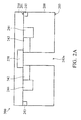
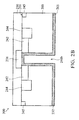
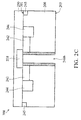
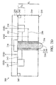
- FIGs. 2A-2D show cross-sectional representations of various stages of forming a semiconductor package structure, in accordance with some embodiments of the disclosure.
- FIG. 2A is an enlarged cross-sectional representation of a region 300 of the semiconductor package structure 100.
- the substrate 200 is provided.
- the materials of the substrate 200 are described above, and thus are omitted here.
- a pair of first guard ring doped regions 242 are formed in the substrate 200.
- a pair of second guard ring doped regions 244 are formed adjacent to the first guard ring doped regions 242. Note that the guard ring doped regions 242 and 244 are adjoined to each other.
- a conductive type of the first guard ring doped regions 242 is different from that of the second guard ring doped regions 244.
- the first guard ring doped regions 242 are n-type guard ring doped regions
- second guard ring doped regions 242 are p-type guard ring doped regions.
- N-type guard ring doped regions comprise n-type heavily (n + ) doped region in a n-well region.
- P-type guard ring doped regions comprise p-type heavily (P + ) doped region in a p-well region.
- the N-type guard ring doped regions 242 are configured to transmit a noise signal with a high frequency, such as in a range from about few MHz to about several GHz.
- the P-type guard ring doped regions 244 are configured to transmit the noise signal with low frequency, such as is in a range from about few MHz to about several GHz. Because the N-type guard ring doped regions 242 and P-type guard ring doped regions 244 are simultaneously formed in the substrate 200, noise signals with a high or low frequency can be transmitted to the ground GND. Therefore, the noise can be effectively decreased.
- a plurality of well regions 245 are formed adjacent to the second guard ring doped regions 244.
- the well regions 245 are p-type well regions.
- An un-doped region between the second guard ring doped regions 244 and the well regions 245 is called a native region.
- the native region is used to increase resistivity without any dopant. The noise may be reduced by higher resistivity.
- the IMD layer 250 is formed on the front side 203 of the substrate 200.
- the poly pattern 238 is formed in the IMD layer 250 and on the front side 203 of the substrate 200. The poly pattern 238 is used as an etching stop layer for a subsequent etching process.
- a photolithography process and an etching process are performed to the substrate 200 from the back side 203 of the substrate 200 until the poly pattern 238 is exposed.
- a trench 240a is thereby formed through the substrate 200.
- the insulating layer 232 is conformally formed lining the back side 203 of the substrate 200, and a bottom surface and sidewalls of the trench 240a as shown in FIG. 2B , in accordance with some embodiments of the disclosure.
- the insulating layer 232 is made of an insulating material, such as oxides or nitrides.
- an etching back process is performed to the back side 203 of the substrate 200 to remove the insulating layer 232 formed on the back side 203 of the substrate 200 and on the bottom surface of the trench 240 as shown in FIG. 2C , in accordance with some embodiments of the disclosure.
- the etching back process is a wet etching process or a dry etching process.
- a conductive material 234 is filled into the through via 240b and on the back side 203 of the substrate 200 as shown in FIG. 2D , in accordance with some embodiments of the disclosure.
- the conductive material 234 is made of copper (Cu), copper alloy, aluminum (Al), aluminum alloys, or combinations thereof.
- the conductive material 234 is formed by plating.
- a polishing process is performed to remove the excess of the conductive material 234 outside of the through via 240b.
- the polishing process is a chemical mechanical polishing (CMP) process. Therefore, the TSV structure 230 including the insulating layer 232 and the conductive material 234 is formed.
- a conductive bump 236 is formed on the conductive material 234.
- the conductive bump 236 is a solder bump.
- conductive material 234 is made of conductive materials with low resistivity, such as solder or solder alloy. Exemplary elements included in the solder alloy include Sn, Pb, Ag, Cu, Ni, Bi or combinations thereof.
- the conductive material 234 has two terminals respectively formed on the front side 201 and back side 203 of the substrate 200. One terminal of the conductive material 234 is connected to the poly pattern 238, and another terminal of the conductive material 234 is connected to the conductive bump 236.
- first and the second guard ring doped regions 242 and 244 are coupled to a ground terminal GND. Therefore, the noise coupling from the substrate 200 or the TSV structure 230 are transmitted to the first and the second guard ring doped regions 242 and 244 and then to the ground terminal GND. For example, the noise coupling from the TSV structure 230 is transmitted to the ground terminal GND through the substrate 200 and the guard ring doped regions 242 and 244, marked by arrow 290 in FIG. 2D .
- the first and second guard ring doped regions 242 and 244 have a depth D 1 in a range from about few hundred nm to about few ⁇ m.
- a ratio (D 1 /H 1 ) of the depth D 1 of the guard ring doped regions to the height H 1 of the through silicon via (TSV) interconnect structure 230 is in a range from 30 ⁇ m to about 100 ⁇ m. If the ratio (D 1 /H 1 ) is too low, less noise is absorbed by second guard ring doped regions 244. If the ratio (D 1 /H 1 ) is too high, less noise is absorbed by second guard ring doped regions 244.
- FIG. 3 shows a cross-sectional representation of a semiconductor package structure, in accordance with some embodiments of the disclosure.
- FIG. 3 is similar to FIG. 2D , the difference between FIG. 2D and FIG. 3 being that a third guard ring doped region 246 is formed adjacent to the second guard ring doped region 244 in FIG. 3 .
- the third guard ring doped region 246 is formed between the well region 245 and the second guard ring doped region 244.
- FIG. 4 shows a cross-sectional representation of a semiconductor package structure, in accordance with some embodiments of the disclosure.
- FIG. 3 is similar to FIG. 2D , the difference between FIG. 2D and FIG. 4 being that a fourth guard ring doped region 248 is formed adjacent to the third guard ring doped region 246 in FIG. 4 .
- the number of guard ring doped regions is not limited to two, three or four, and it may be adjusted according to the actual application.
- Embodiments for forming a semiconductor package structure are provided.
- a through silicon via (TSV) interconnect structure is formed in a substrate.
- At least two guard ring doped regions are formed in a substrate and adjacent to the TSV structure.
- the guard ring doped regions are coupled to a ground terminal.
- the two adjacent guard ring doped regions have different doped regions.
- the n-type guard ring doped region is adjoined to the p-type guard ring doped region.
- the noise signals with high frequency or low frequency from the substrate or the TSV structure can be transmitted to a ground GND by using the guard ring doped regions.
- the semiconductor package structure can be applied to the TSV technology without additional fabrication steps.
- a semiconductor package structure in some embodiments, includes a substrate and the substrate has a front side and a back side.
- the semiconductor package structure includes a through silicon via (TSV) interconnect structure formed in the substrate; and a first guard ring doped region and a second guard ring doped region formed in the substrate, and the first guard ring doped region and the second guard doped region are adjacent to the TSV interconnect structure.
- TSV through silicon via
- a method for forming a semiconductor package structure includes providing a substrate and the substrate has a front side and a back side. The method also includes forming a first guard ring doped region and a second guard ring doped region in the substrate. The method also includes forming a trench through the substrate from a back side of the substrate and conformally forming an insulating layer lining the back side of the substrate, a bottom surface and sidewalls of the trench. The method further includes removing a portion of the insulating layer on the back side of the substrate to form a through via; and forming a conductive material in the through via, wherein a through silicon via (TSV) interconnect structure is formed by the insulating layer and the conductive material.
- TSV through silicon via
Landscapes
- Internal Circuitry In Semiconductor Integrated Circuit Devices (AREA)
- Engineering & Computer Science (AREA)
- Manufacturing & Machinery (AREA)
- Semiconductor Integrated Circuits (AREA)
Abstract
Description
- The present invention relates to a semiconductor package structure, and in particular relates to a semiconductor package structure with a through silicon via (TSV) interconnect structure.
- In electronic engineering, a through silicon via (TSV) is a vertical electrical connection which passes completely through a silicon wafer or die. A TSV is formed by high-performance techniques, when compared to alternatives such as package-on-package. A TSV is used to create three-dimensional (3D) semiconductor packages and 3D integrated circuits. The density of the via of a TSV is substantially higher than the alternatives as the length of connections thereby are shorter.
- An insulating liner of the conventional TSV serves as a capacitor between the silicon wafer and the TSV via plug. In high-speed applications (e.g. RF applications), the electrical impedance of a conventional TSV is reduced due to the insulating liner. When high speed circuits (e.g. digital circuits) transmit signals, the signals are coupled from the high speed circuits to other nodes such as the TSVs of analog circuits. Thus, noise coupling occurs and interferes with the other sensitive circuits (e.g. analog circuits), affecting the overall performance of the semiconductor package, which requires a high clock rate and analog precision.
- Thus, a novel noise coupling suppression structure for a semiconductor package with a TSV interconnect is desirable.
- A detailed description is given in the following embodiments with reference to the accompanying drawings.
- A semiconductor package structure is provided. The semiconductor package structure includes a substrate; a through silicon via (TSV) interconnect structure formed in the substrate; and at least two guard ring doped regions formed in the substrate, wherein the guard ring doped regions are adjacent to the TSV interconnect structure.
- A method for forming a semiconductor package structure is provided. The method includes providing a substrate and forming at least two guard ring doped regions in the substrate. The method also includes forming a trench through the substrate from a back side of the substrate and conformally forming an insulating layer lining the back side of the substrate, a bottom surface and sidewalls of the trench. The method further includes removing a portion of the insulating layer on the back side of the substrate to form a through via; and forming a conductive material in the through via, wherein a through silicon via (TSV) interconnect structure is formed by the insulating layer and the conductive material.
- The present invention can be more fully understood by reading the subsequent detailed description and examples with references made to the accompanying drawings, wherein:
-
FIG. 1 shows a cross-sectional representation of a semiconductor package structure, in accordance with some embodiments of the disclosure. -
FIGs. 2A-2D show cross-sectional representations of various stages of forming a semiconductor package structure, in accordance with some embodiments of the disclosure. -
FIG. 3 shows a cross-sectional representation of a semiconductor package structure, in accordance with some embodiments of the disclosure. -
FIG. 4 shows a cross-sectional representation of a semiconductor package structure, in accordance with some embodiments of the disclosure. - The following disclosure provides many different embodiments, or examples, for implementing different features of the provided subject matter. Specific examples of components and arrangements are described below to simplify the present disclosure. These are, of course, merely examples and are not intended to be limiting. For example, the formation of a first feature over or on a second feature in the description that follows may include embodiments in which the first and second features are formed in direct contact, and may also include embodiments in which additional features may be formed between the first and second features, such that the first and second features may not be in direct contact. In addition, the present disclosure may repeat reference numerals and/or letters in the various examples. This repetition is for the purpose of simplicity and clarity and does not in itself dictate a relationship between the various embodiments and/or configurations discussed.
- Further, spatially relative terms, such as "beneath," "below," "lower," "above," "upper" and the like, may be used herein for ease of description to describe one element or feature's relationship to another element(s) or feature(s) as illustrated in the figures. The spatially relative terms are intended to encompass different orientations of the device in use or operation in addition to the orientation depicted in the figures. The apparatus may be otherwise oriented (rotated 90 degrees or at other orientations) and the spatially relative descriptors used herein may likewise be interpreted accordingly.
- Some variations of the embodiments are described. Throughout the various views and illustrative embodiments, like reference numbers are used to designate like elements. It is understood that additional operations can be provided before, during, and after the method, and some of the operations described can be replaced or eliminated for other embodiments of the method.
-
FIG. 1 shows a cross-sectional representation of asemiconductor package structure 100 which is a noise coupling suppression structure, in accordance with some embodiments of the disclosure. The semiconductor package structure includes asubstrate 200. Thesubstrate 200 has afront side 201 and aback side 203 opposite to thefront side 201. In some embodiments, thesubstrate 200 may be made of silicon or other semiconductor materials. Alternatively or additionally, thesubstrate 200 may include other elementary semiconductor materials such as germanium. In some embodiments, thesubstrate 200 is made of a compound semiconductor such as silicon carbide, gallium arsenic, indium arsenide, or indium phosphide. In some embodiments, thesubstrate 200 is made of an alloy semiconductor such as silicon germanium, silicon germanium carbide, gallium arsenic phosphide, or gallium indium phosphide. In some embodiments, thesubstrate 200 includes an epitaxial layer. For example, thesubstrate 200 has an epitaxial layer overlying a bulk semiconductor. - An
integrated circuit device 220, such as a transistor, is formed on thefront side 201 of thesubstrate 200.Isolation structures 205 are formed in thesubstrate 200 and are used to isolate theintegrated circuit device 220 with other devices (not shown). - A through silicon via (TSV)
interconnect structure 230 is formed through thesubstrate 200, and it is extended from thefront side 201 of thesubstrate 200 to theback side 203 of thesubstrate 200.TSV structure 230 includes aninsulating layer 232 and aconductive material 234. In some other embodiments, a diffusion barrier layer (not shown) is formed between theinsulating layer 232 and theconductive material 234. - The
insulating layer 232 is made of an insulating material, such as oxides or nitrides. Theinsulating layer 232 may be formed by using a plasma enhanced chemical vapor deposition (PECVD) process or another applicable process. In some embodiments, theconductive material 234 is made of copper, copper alloy, aluminum, aluminum alloys, or combinations thereof. In some embodiments, theconductive material 234 is formed by plating. - A
conductive bump 236 is formed on theconductive material 234 and on theback side 203 of thesubstrate 200. Theconductive bump 236 is made of conductive materials, such as copper, copper alloy, aluminum, aluminum alloys, or combinations thereof. - A
poly pattern 238 is formed on theconductive material 234 and on thefront side 201 of thesubstrate 200. Thepoly pattern 238 is used to serves as an etching stop layer - An
interconnect structure 252 is formed on thesubstrate 200. In some embodiments, theinterconnect structure 252 includes contact plugs and conductive features. Conductive features are embedded in an inter-metal dielectric (IMD)layer 250. In some embodiments, theIMD layer 250 is made of silicon oxide. In some embodiments, theIMD layer 250 includes multiple dielectric layers of dielectric materials. Theinterconnect structure 252 shown is merely for illustrative purposes. Theinterconnect structure 252 may include other configurations and may include one or more conductive lines and via layers. - At least two guard ring doped
regions TSV structure 230. As shown inFIG. 1 , a pair of first guard ring dopedregions 242 are formed in thesubstrate 200 and adjacent to theTSV structure 230. A pair of second guard ring dopedregions 244 are formed adjacent to the first guard ring dopedregions 242. The first and second guard ring dopedregions substrate 200 or theTSV structure 230 are transmitted to the first and second guard ring dopedregions FIG. 1 only shows oneTSV structure 230, more than one TSV may be formed to pass through thesubstrate 200. -
FIGs. 2A-2D show cross-sectional representations of various stages of forming a semiconductor package structure, in accordance with some embodiments of the disclosure.FIG. 2A is an enlarged cross-sectional representation of aregion 300 of thesemiconductor package structure 100. - As shown in
FIG. 2A , thesubstrate 200 is provided. The materials of thesubstrate 200 are described above, and thus are omitted here. A pair of first guard ring dopedregions 242 are formed in thesubstrate 200. A pair of second guard ring dopedregions 244 are formed adjacent to the first guard ring dopedregions 242. Note that the guard ring dopedregions - A conductive type of the first guard ring doped
regions 242 is different from that of the second guard ring dopedregions 244. In some embodiments, the first guard ring dopedregions 242 are n-type guard ring doped regions, and second guard ring dopedregions 242 are p-type guard ring doped regions. N-type guard ring doped regions comprise n-type heavily (n+) doped region in a n-well region. P-type guard ring doped regions comprise p-type heavily (P+) doped region in a p-well region. - The N-type guard ring doped
regions 242 are configured to transmit a noise signal with a high frequency, such as in a range from about few MHz to about several GHz. The P-type guard ring dopedregions 244 are configured to transmit the noise signal with low frequency, such as is in a range from about few MHz to about several GHz. Because the N-type guard ring dopedregions 242 and P-type guard ring dopedregions 244 are simultaneously formed in thesubstrate 200, noise signals with a high or low frequency can be transmitted to the ground GND. Therefore, the noise can be effectively decreased. - A plurality of
well regions 245 are formed adjacent to the second guard ring dopedregions 244. In some embodiments, when thesubstrate 200 is a p-type substrate, and thewell regions 245 are p-type well regions. An un-doped region between the second guard ring dopedregions 244 and thewell regions 245 is called a native region. The native region is used to increase resistivity without any dopant. The noise may be reduced by higher resistivity. - After first guard ring doped
regions 242 and second guard ring dopedregions 244 are formed, theIMD layer 250 is formed on thefront side 203 of thesubstrate 200. Afterwards, thepoly pattern 238 is formed in theIMD layer 250 and on thefront side 203 of thesubstrate 200. Thepoly pattern 238 is used as an etching stop layer for a subsequent etching process. - Afterwards, a photolithography process and an etching process are performed to the
substrate 200 from theback side 203 of thesubstrate 200 until thepoly pattern 238 is exposed. Atrench 240a is thereby formed through thesubstrate 200. - After the
trench 240a is formed, the insulatinglayer 232 is conformally formed lining theback side 203 of thesubstrate 200, and a bottom surface and sidewalls of thetrench 240a as shown inFIG. 2B , in accordance with some embodiments of the disclosure. The insulatinglayer 232 is made of an insulating material, such as oxides or nitrides. - After the insulating
layer 232 is formed, an etching back process is performed to theback side 203 of thesubstrate 200 to remove the insulatinglayer 232 formed on theback side 203 of thesubstrate 200 and on the bottom surface of the trench 240 as shown inFIG. 2C , in accordance with some embodiments of the disclosure. As a result, thepoly pattern 238 is exposed and a through via 240b is formed. In some embodiments, the etching back process is a wet etching process or a dry etching process. - After the through via 240b is formed, a
conductive material 234 is filled into the through via 240b and on theback side 203 of thesubstrate 200 as shown inFIG. 2D , in accordance with some embodiments of the disclosure. In some embodiments, theconductive material 234 is made of copper (Cu), copper alloy, aluminum (Al), aluminum alloys, or combinations thereof. In some embodiments, theconductive material 234 is formed by plating. - Afterwards, a polishing process is performed to remove the excess of the
conductive material 234 outside of the through via 240b. In some embodiments, the polishing process is a chemical mechanical polishing (CMP) process. Therefore, theTSV structure 230 including the insulatinglayer 232 and theconductive material 234 is formed. - After the polishing process, a
conductive bump 236 is formed on theconductive material 234. In some embodiments, theconductive bump 236 is a solder bump. In some embodiments,conductive material 234 is made of conductive materials with low resistivity, such as solder or solder alloy. Exemplary elements included in the solder alloy include Sn, Pb, Ag, Cu, Ni, Bi or combinations thereof. - As shown in
FIG. 2D , theconductive material 234 has two terminals respectively formed on thefront side 201 and backside 203 of thesubstrate 200. One terminal of theconductive material 234 is connected to thepoly pattern 238, and another terminal of theconductive material 234 is connected to theconductive bump 236. - It should be noted that the first and the second guard ring doped
regions substrate 200 or theTSV structure 230 are transmitted to the first and the second guard ring dopedregions TSV structure 230 is transmitted to the ground terminal GND through thesubstrate 200 and the guard ring dopedregions arrow 290 inFIG. 2D . - In some embodiments, the first and second guard ring doped
regions interconnect structure 230 is in a range from 30 µm to about 100 µm. If the ratio (D1/H1) is too low, less noise is absorbed by second guard ring dopedregions 244. If the ratio (D1/H1) is too high, less noise is absorbed by second guard ring dopedregions 244. -
FIG. 3 shows a cross-sectional representation of a semiconductor package structure, in accordance with some embodiments of the disclosure.FIG. 3 is similar toFIG. 2D , the difference betweenFIG. 2D andFIG. 3 being that a third guard ring dopedregion 246 is formed adjacent to the second guard ring dopedregion 244 inFIG. 3 . In other words, the third guard ring dopedregion 246 is formed between thewell region 245 and the second guard ring dopedregion 244. -
FIG. 4 shows a cross-sectional representation of a semiconductor package structure, in accordance with some embodiments of the disclosure.FIG. 3 is similar toFIG. 2D , the difference betweenFIG. 2D andFIG. 4 being that a fourth guard ring dopedregion 248 is formed adjacent to the third guard ring dopedregion 246 inFIG. 4 . The number of guard ring doped regions is not limited to two, three or four, and it may be adjusted according to the actual application. - Embodiments for forming a semiconductor package structure are provided. A through silicon via (TSV) interconnect structure is formed in a substrate. At least two guard ring doped regions are formed in a substrate and adjacent to the TSV structure. The guard ring doped regions are coupled to a ground terminal. The two adjacent guard ring doped regions have different doped regions. The n-type guard ring doped region is adjoined to the p-type guard ring doped region. The noise signals with high frequency or low frequency from the substrate or the TSV structure can be transmitted to a ground GND by using the guard ring doped regions. Moreover, the semiconductor package structure can be applied to the TSV technology without additional fabrication steps.
- In some embodiments, a semiconductor package structure is provided. The semiconductor package structure includes a substrate and the substrate has a front side and a back side. The semiconductor package structure includes a through silicon via (TSV) interconnect structure formed in the substrate; and a first guard ring doped region and a second guard ring doped region formed in the substrate, and the first guard ring doped region and the second guard doped region are adjacent to the TSV interconnect structure.
- In some embodiments, a method for forming a semiconductor package structure is provided. The method includes providing a substrate and the substrate has a front side and a back side. The method also includes forming a first guard ring doped region and a second guard ring doped region in the substrate. The method also includes forming a trench through the substrate from a back side of the substrate and conformally forming an insulating layer lining the back side of the substrate, a bottom surface and sidewalls of the trench. The method further includes removing a portion of the insulating layer on the back side of the substrate to form a through via; and forming a conductive material in the through via, wherein a through silicon via (TSV) interconnect structure is formed by the insulating layer and the conductive material.
- While the invention has been described by way of example and in terms of the preferred embodiments, it is to be understood that the invention is not limited to the disclosed embodiments. On the contrary, it is intended to cover various modifications and similar arrangements (as would be apparent to those skilled in the art). Therefore, the scope of the appended claims should be accorded the broadest interpretation so as to encompass all such modifications and similar arrangements.
Claims (15)
- A semiconductor package structure, comprising
a substrate (200), wherein the substrate (200) has a front side (201) and a back side (203);
a through silicon via (TSV) interconnect structure (230) formed in the substrate (200); and
a first guard ring doped region (242) and a second guard ring doped region (244) formed in the substrate (200), wherein the first and the second guard ring doped regions (242, 244) are adjacent to the TSV interconnect structure (230). - The semiconductor package structure as claimed in claim 1, wherein the first guard ring doped region (242) and the second guard ring doped region (244) have different conductive types.
- The semiconductor package structure as claimed in any of claims 1 to 2, further comprising:a third guard ring doped region (246) formed adjacent to the second guard ring doped region (244).
- The semiconductor package structure as claimed in any of claims 1 to 3, wherein the first guard ring doped region (242) is a n-type guard ring doped region and the second guard ring doped region (244) is a p-type guard ring doped region.
- The semiconductor package structure as claimed in any of claims 1 to 4, wherein the first guard ring doped region (242) and the second guard ring doped region (244) are coupled to a ground terminal.
- The semiconductor package structure as claimed in any of claims 1 to 5, wherein the through silicon via (TSV) interconnect structure (230) comprises:a conductive material (234); andan insulating layer (232) surrounding the conductive material (234).
- The semiconductor package structure as claimed in any of claims 1 to 6, further comprising:a well region (245) formed adjacent to the second guard ring doped region (244).
- A method for forming a semiconductor package structure, comprising:providing a substrate (200), wherein the substrate (200) has a front side (201) and a back side (203);forming a first guard ring doped region (242) and a second guard ring doped region (244) in the substrate;forming a trench (240a) through the substrate (200) from the back side (203) of the substrate (200);conformally forming an insulating layer (232) lining the back side (203) of the substrate (200), a bottom surface and sidewalls of the trench (240a);removing a portion of the insulating layer (232) on the back side (203) of the substrate (200) to form a through via (240b); andforming a conductive material (234) in the through via (240b), wherein a through silicon via (TSV) interconnect structure (230) is formed by the insulating layer (232) and the conductive material (234).
- The semiconductor package structure as claimed in claim 8, further comprising:forming a conductive bump (236) on the back side (203) of the substrate (200) and the conductive material (234).
- The semiconductor package structure as claimed in any of claims 8 to 9, before forming the trench (240a) through the substrate (200), further comprising:forming a poly pattern (238) on the front side of the substrate.
- The semiconductor package structure as claimed in any of claims 8 to 10, wherein the first guard ring doped region (242) and the second guard ring doped region (244) have different conductive types.
- The semiconductor package structure as claimed in any of claims 8 to 11, further comprising:forming a well region (245) adjacent to the second guard ring doped region (244).
- The semiconductor package structure as claimed in any of claims 8 to 12 , further comprising:forming a third guard ring doped region (246) adjacent to the second guard ring doped region (244).
- The semiconductor package structure as claimed in claim 13, further comprising:forming a fourth guard ring doped region (248) adjacent to the third guard ring doped region (246), wherein a conductive type of the third guard ring doped region (246) is different from that of the fourth guard ring doped region (248).
- The semiconductor package structure as claimed in any of claims 8 to 14 , wherein forming the first guard ring doped region (242) and the second guard ring doped region (244) adjacent to the first doped region comprises:forming a n-type heavily (n+) doped region in the n-well region; andforming a p-type heavily (p+) doped region in the p-well region.
Applications Claiming Priority (1)
| Application Number | Priority Date | Filing Date | Title |
|---|---|---|---|
| US14/601,440 US9543232B2 (en) | 2015-01-21 | 2015-01-21 | Semiconductor package structure and method for forming the same |
Publications (2)
| Publication Number | Publication Date |
|---|---|
| EP3048642A1 true EP3048642A1 (en) | 2016-07-27 |
| EP3048642B1 EP3048642B1 (en) | 2020-01-08 |
Family
ID=52736986
Family Applications (1)
| Application Number | Title | Priority Date | Filing Date |
|---|---|---|---|
| EP15161244.7A Active EP3048642B1 (en) | 2015-01-21 | 2015-03-27 | Semiconductor package structure and method for forming the same |
Country Status (4)
| Country | Link |
|---|---|
| US (3) | US9543232B2 (en) |
| EP (1) | EP3048642B1 (en) |
| CN (2) | CN105810662B (en) |
| TW (1) | TWI550797B (en) |
Cited By (1)
| Publication number | Priority date | Publication date | Assignee | Title |
|---|---|---|---|---|
| KR20220010852A (en) * | 2020-07-20 | 2022-01-27 | 삼성전자주식회사 | Semiconductor device and method of manufacturing the semiconductor device |
Families Citing this family (8)
| Publication number | Priority date | Publication date | Assignee | Title |
|---|---|---|---|---|
| US9543232B2 (en) * | 2015-01-21 | 2017-01-10 | Mediatek Inc. | Semiconductor package structure and method for forming the same |
| KR102450580B1 (en) | 2017-12-22 | 2022-10-07 | 삼성전자주식회사 | Semiconductor Device having a Structure for Insulating Layer under Metal Line |
| US11257943B2 (en) * | 2019-06-17 | 2022-02-22 | Fuji Electric Co., Ltd. | Semiconductor device |
| CN111816657B (en) * | 2020-07-02 | 2021-08-03 | 长江存储科技有限责任公司 | A semiconductor device and method of making the same |
| CN115394734A (en) * | 2021-05-21 | 2022-11-25 | 长鑫存储技术有限公司 | Semiconductor structure and preparation method thereof |
| EP4117030A4 (en) * | 2021-05-21 | 2023-02-08 | Changxin Memory Technologies, Inc. | SEMI-CONDUCTOR STRUCTURE AND METHOD OF MANUFACTURING IT |
| CN115472584B (en) * | 2022-09-02 | 2025-10-28 | 武汉新芯集成电路股份有限公司 | Semiconductor device and method for manufacturing the same |
| EP4336553A1 (en) * | 2022-09-08 | 2024-03-13 | Samsung Electronics Co., Ltd. | Integrated circuit devices including via capacitors |
Citations (5)
| Publication number | Priority date | Publication date | Assignee | Title |
|---|---|---|---|---|
| US20100237386A1 (en) * | 2009-03-20 | 2010-09-23 | Industrial Technology Research Institute | Electrostatic discharge structure for 3-dimensional integrated circuit through-silicon via device |
| KR20110006946A (en) * | 2009-07-15 | 2011-01-21 | 주식회사 하이닉스반도체 | Semiconductor chip with low noise through silicon via passing through guard ring and stacked package using same |
| US20110260330A1 (en) * | 2010-04-27 | 2011-10-27 | Ji-Tai Seo | Semiconductor integrated circuit |
| US20130154048A1 (en) * | 2011-12-16 | 2013-06-20 | Taiwan Semiconductor Manufacturing Company, Ltd. | Guard Ring for Through Vias |
| US20130264676A1 (en) * | 2012-04-10 | 2013-10-10 | Mediatek Inc. | Semiconductor package with through silicon via interconnect and method for fabricating the same |
Family Cites Families (10)
| Publication number | Priority date | Publication date | Assignee | Title |
|---|---|---|---|---|
| US7492018B2 (en) * | 2004-09-17 | 2009-02-17 | Taiwan Semiconductor Manufacturing Company, Ltd. | Isolating substrate noise by forming semi-insulating regions |
| US7956442B2 (en) * | 2008-10-09 | 2011-06-07 | Taiwan Semiconductor Manufacturing Company, Ltd. | Backside connection to TSVs having redistribution lines |
| TWI413236B (en) * | 2010-06-11 | 2013-10-21 | 財團法人工業技術研究院 | Electrostatic discharge protection scheme for stacking process of semiconductor devices |
| US8502338B2 (en) * | 2010-09-09 | 2013-08-06 | Taiwan Semiconductor Manufacturing Company, Ltd. | Through-substrate via waveguides |
| US8928127B2 (en) * | 2010-09-24 | 2015-01-06 | Taiwan Semiconductor Manufacturing Company, Ltd. | Noise decoupling structure with through-substrate vias |
| US8546953B2 (en) | 2011-12-13 | 2013-10-01 | Taiwan Semiconductor Manufacturing Co., Ltd. | Through silicon via (TSV) isolation structures for noise reduction in 3D integrated circuit |
| CN103050424B (en) * | 2012-08-17 | 2016-01-20 | 上海华虹宏力半导体制造有限公司 | The guard ring of semiconductor device |
| KR102013770B1 (en) * | 2012-08-30 | 2019-08-23 | 에스케이하이닉스 주식회사 | Semiconductor device and method for fabricating the same |
| US9219038B2 (en) * | 2013-03-12 | 2015-12-22 | Taiwan Semiconductor Manufacturing Co., Ltd. | Shielding for through-silicon-via |
| US9543232B2 (en) * | 2015-01-21 | 2017-01-10 | Mediatek Inc. | Semiconductor package structure and method for forming the same |
-
2015
- 2015-01-21 US US14/601,440 patent/US9543232B2/en active Active
- 2015-03-27 EP EP15161244.7A patent/EP3048642B1/en active Active
- 2015-09-03 TW TW104129120A patent/TWI550797B/en not_active IP Right Cessation
- 2015-09-14 CN CN201510582231.2A patent/CN105810662B/en active Active
- 2015-09-14 CN CN201810460813.7A patent/CN108461466B/en active Active
-
2016
- 2016-11-30 US US15/365,394 patent/US9899261B2/en active Active
- 2016-11-30 US US15/365,435 patent/US9786560B2/en active Active
Patent Citations (5)
| Publication number | Priority date | Publication date | Assignee | Title |
|---|---|---|---|---|
| US20100237386A1 (en) * | 2009-03-20 | 2010-09-23 | Industrial Technology Research Institute | Electrostatic discharge structure for 3-dimensional integrated circuit through-silicon via device |
| KR20110006946A (en) * | 2009-07-15 | 2011-01-21 | 주식회사 하이닉스반도체 | Semiconductor chip with low noise through silicon via passing through guard ring and stacked package using same |
| US20110260330A1 (en) * | 2010-04-27 | 2011-10-27 | Ji-Tai Seo | Semiconductor integrated circuit |
| US20130154048A1 (en) * | 2011-12-16 | 2013-06-20 | Taiwan Semiconductor Manufacturing Company, Ltd. | Guard Ring for Through Vias |
| US20130264676A1 (en) * | 2012-04-10 | 2013-10-10 | Mediatek Inc. | Semiconductor package with through silicon via interconnect and method for fabricating the same |
Cited By (1)
| Publication number | Priority date | Publication date | Assignee | Title |
|---|---|---|---|---|
| KR20220010852A (en) * | 2020-07-20 | 2022-01-27 | 삼성전자주식회사 | Semiconductor device and method of manufacturing the semiconductor device |
Also Published As
| Publication number | Publication date |
|---|---|
| US9899261B2 (en) | 2018-02-20 |
| EP3048642B1 (en) | 2020-01-08 |
| CN105810662A (en) | 2016-07-27 |
| TWI550797B (en) | 2016-09-21 |
| CN108461466A (en) | 2018-08-28 |
| US20170084525A1 (en) | 2017-03-23 |
| CN108461466B (en) | 2020-03-10 |
| TW201628149A (en) | 2016-08-01 |
| CN105810662B (en) | 2018-06-29 |
| US9543232B2 (en) | 2017-01-10 |
| US20160211194A1 (en) | 2016-07-21 |
| US9786560B2 (en) | 2017-10-10 |
| US20170084488A1 (en) | 2017-03-23 |
Similar Documents
| Publication | Publication Date | Title |
|---|---|---|
| US9899261B2 (en) | Semiconductor package structure and method for forming the same | |
| US9269664B2 (en) | Semiconductor package with through silicon via interconnect and method for fabricating the same | |
| US10199273B2 (en) | Method for forming semiconductor device with through silicon via | |
| US8502338B2 (en) | Through-substrate via waveguides | |
| CN103378034B (en) | Semiconductor package with TSV interconnects | |
| CN104425453B (en) | 3DIC interconnection means and method | |
| US9978637B2 (en) | Mechanism for forming patterned metal pad connected to multiple through silicon vias (TSVs) | |
| US20170263667A1 (en) | Semiconductor Devices, Methods of Manufacturing Thereof, and Image Sensor Devices | |
| KR20130053338A (en) | Integrated circuit device having through silicon via structure | |
| US20150303108A1 (en) | Method for forming semiconductor device | |
| US11887913B2 (en) | Integrated circuit device and semiconductor package including the same | |
| CN103515302B (en) | Semiconductor device and method of manufacture | |
| CN105321904B (en) | Semiconductor device | |
| TWI708325B (en) | Semiconductor structure and fabrication method thereof |
Legal Events
| Date | Code | Title | Description |
|---|---|---|---|
| PUAI | Public reference made under article 153(3) epc to a published international application that has entered the european phase |
Free format text: ORIGINAL CODE: 0009012 |
|
| AK | Designated contracting states |
Kind code of ref document: A1 Designated state(s): AL AT BE BG CH CY CZ DE DK EE ES FI FR GB GR HR HU IE IS IT LI LT LU LV MC MK MT NL NO PL PT RO RS SE SI SK SM TR |
|
| AX | Request for extension of the european patent |
Extension state: BA ME |
|
| STAA | Information on the status of an ep patent application or granted ep patent |
Free format text: STATUS: REQUEST FOR EXAMINATION WAS MADE |
|
| 17P | Request for examination filed |
Effective date: 20170118 |
|
| RBV | Designated contracting states (corrected) |
Designated state(s): AL AT BE BG CH CY CZ DE DK EE ES FI FR GB GR HR HU IE IS IT LI LT LU LV MC MK MT NL NO PL PT RO RS SE SI SK SM TR |
|
| GRAP | Despatch of communication of intention to grant a patent |
Free format text: ORIGINAL CODE: EPIDOSNIGR1 |
|
| STAA | Information on the status of an ep patent application or granted ep patent |
Free format text: STATUS: GRANT OF PATENT IS INTENDED |
|
| INTG | Intention to grant announced |
Effective date: 20190731 |
|
| GRAS | Grant fee paid |
Free format text: ORIGINAL CODE: EPIDOSNIGR3 |
|
| GRAA | (expected) grant |
Free format text: ORIGINAL CODE: 0009210 |
|
| STAA | Information on the status of an ep patent application or granted ep patent |
Free format text: STATUS: THE PATENT HAS BEEN GRANTED |
|
| AK | Designated contracting states |
Kind code of ref document: B1 Designated state(s): AL AT BE BG CH CY CZ DE DK EE ES FI FR GB GR HR HU IE IS IT LI LT LU LV MC MK MT NL NO PL PT RO RS SE SI SK SM TR |
|
| REG | Reference to a national code |
Ref country code: GB Ref legal event code: FG4D |
|
| REG | Reference to a national code |
Ref country code: CH Ref legal event code: EP |
|
| REG | Reference to a national code |
Ref country code: DE Ref legal event code: R096 Ref document number: 602015045019 Country of ref document: DE |
|
| REG | Reference to a national code |
Ref country code: IE Ref legal event code: FG4D |
|
| REG | Reference to a national code |
Ref country code: AT Ref legal event code: REF Ref document number: 1223741 Country of ref document: AT Kind code of ref document: T Effective date: 20200215 |
|
| REG | Reference to a national code |
Ref country code: NL Ref legal event code: MP Effective date: 20200108 |
|
| REG | Reference to a national code |
Ref country code: LT Ref legal event code: MG4D |
|
| PG25 | Lapsed in a contracting state [announced via postgrant information from national office to epo] |
Ref country code: RS Free format text: LAPSE BECAUSE OF FAILURE TO SUBMIT A TRANSLATION OF THE DESCRIPTION OR TO PAY THE FEE WITHIN THE PRESCRIBED TIME-LIMIT Effective date: 20200108 Ref country code: NO Free format text: LAPSE BECAUSE OF FAILURE TO SUBMIT A TRANSLATION OF THE DESCRIPTION OR TO PAY THE FEE WITHIN THE PRESCRIBED TIME-LIMIT Effective date: 20200408 Ref country code: PT Free format text: LAPSE BECAUSE OF FAILURE TO SUBMIT A TRANSLATION OF THE DESCRIPTION OR TO PAY THE FEE WITHIN THE PRESCRIBED TIME-LIMIT Effective date: 20200531 Ref country code: FI Free format text: LAPSE BECAUSE OF FAILURE TO SUBMIT A TRANSLATION OF THE DESCRIPTION OR TO PAY THE FEE WITHIN THE PRESCRIBED TIME-LIMIT Effective date: 20200108 Ref country code: NL Free format text: LAPSE BECAUSE OF FAILURE TO SUBMIT A TRANSLATION OF THE DESCRIPTION OR TO PAY THE FEE WITHIN THE PRESCRIBED TIME-LIMIT Effective date: 20200108 Ref country code: LT Free format text: LAPSE BECAUSE OF FAILURE TO SUBMIT A TRANSLATION OF THE DESCRIPTION OR TO PAY THE FEE WITHIN THE PRESCRIBED TIME-LIMIT Effective date: 20200108 |
|
| PG25 | Lapsed in a contracting state [announced via postgrant information from national office to epo] |
Ref country code: LV Free format text: LAPSE BECAUSE OF FAILURE TO SUBMIT A TRANSLATION OF THE DESCRIPTION OR TO PAY THE FEE WITHIN THE PRESCRIBED TIME-LIMIT Effective date: 20200108 Ref country code: SE Free format text: LAPSE BECAUSE OF FAILURE TO SUBMIT A TRANSLATION OF THE DESCRIPTION OR TO PAY THE FEE WITHIN THE PRESCRIBED TIME-LIMIT Effective date: 20200108 Ref country code: HR Free format text: LAPSE BECAUSE OF FAILURE TO SUBMIT A TRANSLATION OF THE DESCRIPTION OR TO PAY THE FEE WITHIN THE PRESCRIBED TIME-LIMIT Effective date: 20200108 Ref country code: BG Free format text: LAPSE BECAUSE OF FAILURE TO SUBMIT A TRANSLATION OF THE DESCRIPTION OR TO PAY THE FEE WITHIN THE PRESCRIBED TIME-LIMIT Effective date: 20200408 Ref country code: IS Free format text: LAPSE BECAUSE OF FAILURE TO SUBMIT A TRANSLATION OF THE DESCRIPTION OR TO PAY THE FEE WITHIN THE PRESCRIBED TIME-LIMIT Effective date: 20200508 Ref country code: GR Free format text: LAPSE BECAUSE OF FAILURE TO SUBMIT A TRANSLATION OF THE DESCRIPTION OR TO PAY THE FEE WITHIN THE PRESCRIBED TIME-LIMIT Effective date: 20200409 |
|
| REG | Reference to a national code |
Ref country code: DE Ref legal event code: R097 Ref document number: 602015045019 Country of ref document: DE |
|
| PG25 | Lapsed in a contracting state [announced via postgrant information from national office to epo] |
Ref country code: SK Free format text: LAPSE BECAUSE OF FAILURE TO SUBMIT A TRANSLATION OF THE DESCRIPTION OR TO PAY THE FEE WITHIN THE PRESCRIBED TIME-LIMIT Effective date: 20200108 Ref country code: RO Free format text: LAPSE BECAUSE OF FAILURE TO SUBMIT A TRANSLATION OF THE DESCRIPTION OR TO PAY THE FEE WITHIN THE PRESCRIBED TIME-LIMIT Effective date: 20200108 Ref country code: CZ Free format text: LAPSE BECAUSE OF FAILURE TO SUBMIT A TRANSLATION OF THE DESCRIPTION OR TO PAY THE FEE WITHIN THE PRESCRIBED TIME-LIMIT Effective date: 20200108 Ref country code: MC Free format text: LAPSE BECAUSE OF FAILURE TO SUBMIT A TRANSLATION OF THE DESCRIPTION OR TO PAY THE FEE WITHIN THE PRESCRIBED TIME-LIMIT Effective date: 20200108 Ref country code: ES Free format text: LAPSE BECAUSE OF FAILURE TO SUBMIT A TRANSLATION OF THE DESCRIPTION OR TO PAY THE FEE WITHIN THE PRESCRIBED TIME-LIMIT Effective date: 20200108 Ref country code: DK Free format text: LAPSE BECAUSE OF FAILURE TO SUBMIT A TRANSLATION OF THE DESCRIPTION OR TO PAY THE FEE WITHIN THE PRESCRIBED TIME-LIMIT Effective date: 20200108 Ref country code: SM Free format text: LAPSE BECAUSE OF FAILURE TO SUBMIT A TRANSLATION OF THE DESCRIPTION OR TO PAY THE FEE WITHIN THE PRESCRIBED TIME-LIMIT Effective date: 20200108 Ref country code: EE Free format text: LAPSE BECAUSE OF FAILURE TO SUBMIT A TRANSLATION OF THE DESCRIPTION OR TO PAY THE FEE WITHIN THE PRESCRIBED TIME-LIMIT Effective date: 20200108 |
|
| REG | Reference to a national code |
Ref country code: CH Ref legal event code: PL |
|
| PLBE | No opposition filed within time limit |
Free format text: ORIGINAL CODE: 0009261 |
|
| STAA | Information on the status of an ep patent application or granted ep patent |
Free format text: STATUS: NO OPPOSITION FILED WITHIN TIME LIMIT |
|
| REG | Reference to a national code |
Ref country code: AT Ref legal event code: MK05 Ref document number: 1223741 Country of ref document: AT Kind code of ref document: T Effective date: 20200108 |
|
| 26N | No opposition filed |
Effective date: 20201009 |
|
| REG | Reference to a national code |
Ref country code: BE Ref legal event code: MM Effective date: 20200331 |
|
| PG25 | Lapsed in a contracting state [announced via postgrant information from national office to epo] |
Ref country code: LU Free format text: LAPSE BECAUSE OF NON-PAYMENT OF DUE FEES Effective date: 20200327 |
|
| PG25 | Lapsed in a contracting state [announced via postgrant information from national office to epo] |
Ref country code: AT Free format text: LAPSE BECAUSE OF FAILURE TO SUBMIT A TRANSLATION OF THE DESCRIPTION OR TO PAY THE FEE WITHIN THE PRESCRIBED TIME-LIMIT Effective date: 20200108 Ref country code: LI Free format text: LAPSE BECAUSE OF NON-PAYMENT OF DUE FEES Effective date: 20200331 Ref country code: IE Free format text: LAPSE BECAUSE OF NON-PAYMENT OF DUE FEES Effective date: 20200327 Ref country code: CH Free format text: LAPSE BECAUSE OF NON-PAYMENT OF DUE FEES Effective date: 20200331 Ref country code: IT Free format text: LAPSE BECAUSE OF FAILURE TO SUBMIT A TRANSLATION OF THE DESCRIPTION OR TO PAY THE FEE WITHIN THE PRESCRIBED TIME-LIMIT Effective date: 20200108 |
|
| PG25 | Lapsed in a contracting state [announced via postgrant information from national office to epo] |
Ref country code: BE Free format text: LAPSE BECAUSE OF NON-PAYMENT OF DUE FEES Effective date: 20200331 Ref country code: PL Free format text: LAPSE BECAUSE OF FAILURE TO SUBMIT A TRANSLATION OF THE DESCRIPTION OR TO PAY THE FEE WITHIN THE PRESCRIBED TIME-LIMIT Effective date: 20200108 Ref country code: SI Free format text: LAPSE BECAUSE OF FAILURE TO SUBMIT A TRANSLATION OF THE DESCRIPTION OR TO PAY THE FEE WITHIN THE PRESCRIBED TIME-LIMIT Effective date: 20200108 |
|
| PG25 | Lapsed in a contracting state [announced via postgrant information from national office to epo] |
Ref country code: TR Free format text: LAPSE BECAUSE OF FAILURE TO SUBMIT A TRANSLATION OF THE DESCRIPTION OR TO PAY THE FEE WITHIN THE PRESCRIBED TIME-LIMIT Effective date: 20200108 Ref country code: MT Free format text: LAPSE BECAUSE OF FAILURE TO SUBMIT A TRANSLATION OF THE DESCRIPTION OR TO PAY THE FEE WITHIN THE PRESCRIBED TIME-LIMIT Effective date: 20200108 Ref country code: CY Free format text: LAPSE BECAUSE OF FAILURE TO SUBMIT A TRANSLATION OF THE DESCRIPTION OR TO PAY THE FEE WITHIN THE PRESCRIBED TIME-LIMIT Effective date: 20200108 |
|
| PG25 | Lapsed in a contracting state [announced via postgrant information from national office to epo] |
Ref country code: MK Free format text: LAPSE BECAUSE OF FAILURE TO SUBMIT A TRANSLATION OF THE DESCRIPTION OR TO PAY THE FEE WITHIN THE PRESCRIBED TIME-LIMIT Effective date: 20200108 Ref country code: AL Free format text: LAPSE BECAUSE OF FAILURE TO SUBMIT A TRANSLATION OF THE DESCRIPTION OR TO PAY THE FEE WITHIN THE PRESCRIBED TIME-LIMIT Effective date: 20200108 |
|
| P01 | Opt-out of the competence of the unified patent court (upc) registered |
Effective date: 20230607 |
|
| REG | Reference to a national code |
Ref country code: DE Ref legal event code: R079 Ref document number: 602015045019 Country of ref document: DE Free format text: PREVIOUS MAIN CLASS: H01L0021768000 Ipc: H10W0020000000 |
|
| PGFP | Annual fee paid to national office [announced via postgrant information from national office to epo] |
Ref country code: FR Payment date: 20251231 Year of fee payment: 12 |
|
| PGFP | Annual fee paid to national office [announced via postgrant information from national office to epo] |
Ref country code: GB Payment date: 20260106 Year of fee payment: 12 |
|
| PGFP | Annual fee paid to national office [announced via postgrant information from national office to epo] |
Ref country code: DE Payment date: 20260102 Year of fee payment: 12 |