EP3048638A1 - Etching method - Google Patents
Etching method Download PDFInfo
- Publication number
- EP3048638A1 EP3048638A1 EP14846557.8A EP14846557A EP3048638A1 EP 3048638 A1 EP3048638 A1 EP 3048638A1 EP 14846557 A EP14846557 A EP 14846557A EP 3048638 A1 EP3048638 A1 EP 3048638A1
- Authority
- EP
- European Patent Office
- Prior art keywords
- polymer
- layer
- etching
- gas
- region
- Prior art date
- Legal status (The legal status is an assumption and is not a legal conclusion. Google has not performed a legal analysis and makes no representation as to the accuracy of the status listed.)
- Withdrawn
Links
Images




Classifications
-
- H—ELECTRICITY
- H10—SEMICONDUCTOR DEVICES; ELECTRIC SOLID-STATE DEVICES NOT OTHERWISE PROVIDED FOR
- H10P—GENERIC PROCESSES OR APPARATUS FOR THE MANUFACTURE OR TREATMENT OF DEVICES COVERED BY CLASS H10
- H10P50/00—Etching of wafers, substrates or parts of devices
- H10P50/73—Etching of wafers, substrates or parts of devices using masks for insulating materials
-
- H—ELECTRICITY
- H01—ELECTRIC ELEMENTS
- H01J—ELECTRIC DISCHARGE TUBES OR DISCHARGE LAMPS
- H01J37/00—Discharge tubes with provision for introducing objects or material to be exposed to the discharge, e.g. for the purpose of examination or processing thereof
- H01J37/32—Gas-filled discharge tubes
- H01J37/32009—Arrangements for generation of plasma specially adapted for examination or treatment of objects, e.g. plasma sources
- H01J37/32082—Radio frequency generated discharge
-
- H—ELECTRICITY
- H01—ELECTRIC ELEMENTS
- H01J—ELECTRIC DISCHARGE TUBES OR DISCHARGE LAMPS
- H01J37/00—Discharge tubes with provision for introducing objects or material to be exposed to the discharge, e.g. for the purpose of examination or processing thereof
- H01J37/32—Gas-filled discharge tubes
- H01J37/32009—Arrangements for generation of plasma specially adapted for examination or treatment of objects, e.g. plasma sources
- H01J37/32192—Microwave generated discharge
-
- H—ELECTRICITY
- H10—SEMICONDUCTOR DEVICES; ELECTRIC SOLID-STATE DEVICES NOT OTHERWISE PROVIDED FOR
- H10P—GENERIC PROCESSES OR APPARATUS FOR THE MANUFACTURE OR TREATMENT OF DEVICES COVERED BY CLASS H10
- H10P50/00—Etching of wafers, substrates or parts of devices
- H10P50/20—Dry etching; Plasma etching; Reactive-ion etching
- H10P50/28—Dry etching; Plasma etching; Reactive-ion etching of insulating materials
- H10P50/286—Dry etching; Plasma etching; Reactive-ion etching of insulating materials of organic materials
- H10P50/287—Dry etching; Plasma etching; Reactive-ion etching of insulating materials of organic materials by chemical means
-
- H—ELECTRICITY
- H10—SEMICONDUCTOR DEVICES; ELECTRIC SOLID-STATE DEVICES NOT OTHERWISE PROVIDED FOR
- H10P—GENERIC PROCESSES OR APPARATUS FOR THE MANUFACTURE OR TREATMENT OF DEVICES COVERED BY CLASS H10
- H10P76/00—Manufacture or treatment of masks on semiconductor bodies, e.g. by lithography or photolithography
- H10P76/40—Manufacture or treatment of masks on semiconductor bodies, e.g. by lithography or photolithography of masks comprising inorganic materials
- H10P76/408—Manufacture or treatment of masks on semiconductor bodies, e.g. by lithography or photolithography of masks comprising inorganic materials characterised by their sizes, orientations, dispositions, behaviours or shapes
- H10P76/4085—Manufacture or treatment of masks on semiconductor bodies, e.g. by lithography or photolithography of masks comprising inorganic materials characterised by their sizes, orientations, dispositions, behaviours or shapes characterised by the processes involved to create the masks
-
- B—PERFORMING OPERATIONS; TRANSPORTING
- B82—NANOTECHNOLOGY
- B82Y—SPECIFIC USES OR APPLICATIONS OF NANOSTRUCTURES; MEASUREMENT OR ANALYSIS OF NANOSTRUCTURES; MANUFACTURE OR TREATMENT OF NANOSTRUCTURES
- B82Y40/00—Manufacture or treatment of nanostructures
Definitions
- An exemplary embodiment of the present disclosure relates to an etching method.
- EUV extreme ultraviolet
- a light having a remarkably short wavelength e.g ., 13.5 nm
- the EUV there is a technical barrier against mass production.
- the EUV has a problem such as a long exposure time.
- a block copolymer layer is coated on a base layer.
- the block copolymer layer contains a block copolymer containing two or more polymer block components A and B which are immiscible with each other.
- a heat treatment annealing
- a heat treatment is performed to cause the polymer block components A and B to spontaneously phase-separate from each other.
- an ordered pattern having a first region containing the polymer block component A and a second region containing the polymer block component B, is obtained.
- a patterning processing of block copolymers has been suggested as a method of forming a via. In the patterning processing described in Patent Document 2, a pattern is obtained by removing the second region among the first region and the second region of the phase-separated block copolymer layer.
- a method of etching an etching target layer of a workpiece includes a step (a) of forming a self-assemblable block copolymer layer containing a first polymer and a second polymer on an intermediate layer formed on the etching target layer; a step (b) of processing the workpiece to form a first region containing the first polymer and a second region containing the second polymer, from the block copolymer layer; after the step (b), a step (c) of forming a mask by etching the second region and the intermediate layer just below the second region; after the step (c), a step (d) of forming a protective film on the mask by generating plasma of a processing gas containing silicon tetrachloride gas and oxygen gas within a processing container of a plasma processing apparatus that accommodates the workpiece; and after the step (d), a step (e) of etching the etching target layer.
- a protective film is formed on the mask.
- the protective film contains silicon oxide based on oxygen and silicon in the plasma generated in the step (d). Owing to the protective film, the mask is protected from the etching in the step (e). Accordingly, it is possible to suppress the mask from being deformed due to the etching of the etching target layer.
- the etching target layer is a silicon-containing layer.
- plasma of a processing gas containing at least one of fluorocarbon gas and fluorohydrocarbon gas may be generated within the processing container.
- a method of etching an etching target layer of a workpiece includes a step (a) of forming a self-assemblable block copolymer layer containing a first polymer and a second polymer on an intermediate layer formed on the etching target layer; a step (b) of processing the workpiece to form a first region containing the first polymer and a second region containing the second polymer, from the block copolymer layer; after the step (b), a step (c) of forming a mask by etching the second region and the intermediate layer just below the second region; after the forming the mask, a step (f) of etching the etching target layer.
- the etching target layer which is a subject to be etched in this method, is a layer containing silicon oxide or silicon nitride.
- a protective layer which contains components such as SiBrO derived from active species of atoms or molecules contained in hydrogen bromide gas contained in the gas used in the step (f). Further, the mask is modified, that is, cured by the active species of Br. As a result, it is possible to suppress the mask from being deformed due to the etching of the etching target layer.
- the first polymer may be polystyrene
- the second polymer may be poly(methyl methacrylate).
- the mask obtained by the patterning of the block copolymer may be suppressed from being deformed due to the etching of the etching target layer.
- FIG. 1 is a flowchart illustrating an etching method according to an exemplary embodiment.
- FIG 2 , FIG. 3 , and FIG. 4 are views illustrating a cross-section of a product prepared in each step illustrated in FIG. 1 .
- etching method MT1 according to an exemplary embodiment includes step ST1, step ST2, step ST3, step ST4, step ST5, and step ST6.
- step ST1 first of all, in step ST1, an intermediate layer NL is formed on a surface of a workpiece (hereinafter, referred to as a "wafer") W.
- the wafer W includes a substrate Sb and an etching target layer EL.
- the substrate Sb is made of, for example, silicon.
- the etching target layer EL is formed on the substrate Sb.
- the etching target layer EL is a silicon-containing layer.
- the etching target layer EL may be a SiN layer, a silicon oxide layer, or a silicon-containing resist layer. Further, the etching target layer EL may have a film thickness of, for example, 15 nm to 20 nm.
- an organic film OL is coated on the etching target layer EL.
- the organic film OL is a block copolymer of, for example, styrene and methyl methacrylate.
- the wafer W is subjected to a heat treatment after the coating.
- the proper value of the heat treatment temperature depends on the kind of the organic film OL, but is usually about 200 °C to 300 °C.
- the heat treatment temperature is, for example, 250 °C.
- the organic film OL is generally reduced, and an intermediate layer NL and an altered layer RL are formed from the organic layer OL. Meanwhile, the altered layer RL is a layer in which carbon in the organic layer OL is altered.
- the altered layer RL is chemically removed by a development treatment. Therefore, the intermediate layer NL is formed on the etching target layer EL.
- the surface of the intermediate layer NL has a neutral state that is neither hydrophobic nor hydrophilic.
- Polymers in a block copolymer layer (to be described later) have a strong hydrophilicity if the polymer length is short, or strong hydrophobicity if the polymer length is long. Thus, since there are a strong hydrophilic type and a strong hydrophobic type in the polymers, the polymers may be phase-separated in a desired shape by forming the intermediate layer NL having a neutral surface.
- step ST2 is subsequently performed.
- a block copolymer is coated on the surface of the wafer W, that is, the surface of the intermediate layer NL.
- the block copolymer may be coated by various methods such as, for example, a spin coat method. Therefore, as illustrated in FIG. 3(a) , a block copolymer layer BCL is formed on the surface of the intermediate layer NL.
- the block copolymer is a self-assembled block copolymer, and includes a first polymer and a second polymer.
- the block copolymer is polystyrene-block-poly(methyl methacrylate) (PS-b-PMMA).
- PS-b-PMMA includes polystyrene (PS) as the first polymer, and poly(methyl methacrylate) (PMMA) as the second polymer.
- PS-b-PMMA both of PS and PMMA are polymers in which one molecule has a diameter of 0.7 nm.
- a block copolymer containing PS and PMMA, which are immiscible with each other is coated on the intermediate layer NL to form the block copolymer layer BCL, and then, the wafer W is subjected to a heat treatment (annealing) at normal temperature (25 °C) to 300 °C or less, a phase separation occurs in the block copolymer layer BCL.
- the heat treatment is performed at a temperature higher than 300 °C, so that PS and PMMA are randomly arranged. Further, even though the temperature is returned to normal temperature after the phase separation, the block copolymer layer BCL is maintained in the phase-separated state.
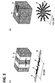
- FIG. 5(a) illustrates a phase-separated structure in which Polymer A and Polymer B have substantially the same polymer length.
- Polymer A is PS and Polymer B is PMMA.
- the interaction of each polymer is the same.
- Polymer A and Polymer B are self-assembled and phase-separated linearly. That is, Polymer A forms first linear regions, and Polymer B forms second linear regions, each of which is located between the first regions.
- a periodic pattern of lines and spaces L/S may be formed. The periodic pattern may be applied as a pattern for manufacturing devices such as semiconductor devices.
- FIG. 5(b) illustrates a phase-separated structure in which Polymer A and Polymer B are considerably different in polymer length, that is, the polymer length of Polymer A is longer than the polymer length of Polymer B.
- the interaction (repulsive force) of Polymer A is stronger, and the interaction (repulsive force) of Polymer B is weaker.
- the block copolymer layer BCL is subjected to a heat treatment at about 250 °C, due to the difference in strength of the interaction between the polymers, Polymer A is self-assembled outward and Polymer B is self-assembled inward.
- Polymer B is self-assembled in a cylindrical shape to thereby form a second region
- Polymer A is self-assembled to surround the cylindrical region, to thereby form a first region.
- a periodic pattern of holes may be formed. This periodic pattern may also be applied as a pattern for manufacturing devices such as semiconductor devices.
- step ST3 of method MT1 a treatment for the phase separation of the block copolymer layer BCL is performed.
- step ST2 of an exemplary embodiment the wafer W is heated at a temperature of 200 °C to 300 °C, so that phase separation occurs in the block copolymer layer BCL.
- step ST3 as illustrated in FIG. 3(b) , first regions R1 containing the first polymer and second regions R2 containing the second polymer are formed in the block copolymer layer BCL.
- the first regions R1 and the second regions R2 may be alternated to form a line pattern.
- the second region R2 may be a cylindrical region, and the first region R1 may surround the cylindrical second region R2.
- FIG. 6 is a view schematically illustrating an exemplary embodiment of a plasma processing apparatus which may be used for performing method MT1.
- the plasma processing apparatus 1 illustrated in FIG. 6 is a capacitively coupled parallel plate type plasma processing apparatus, and is provided with a substantially cylindrical chamber (processing container) 10.
- the chamber 10 is grounded.
- the inner surface of the chamber 10 is subjected to an anodizing treatment (anodic oxidation treatment).
- the chamber 10 is grounded.
- a cylindrical susceptor support 14 is disposed via an insulating plate 12 made of, for example, ceramic.
- a susceptor 16 made of, for example, aluminum is provided on the susceptor support 14.
- an electrostatic chuck 18 is provided to hold the wafer W by electrostatic attraction force.
- the electrostatic chuck 18 has a structure where a chuck electrode 20 made of a conductive film is interposed between a pair of insulating layers or insulating sheets.
- the electrode 20 is electrically connected with a DC power source 22 via a switch 24.
- the wafer W is able to be attracted and held on the electrostatic chuck 19 by electrostatic attraction force generated by a DC voltage from the DC power source 22.
- a focus ring 26 is disposed around the electrostatic chuck 18 on the susceptor 16 to enhance in-plane uniformity of the etching.
- the focus ring 26 is made of, for example, silicon.
- a cylindrical inner wall member 28 made of, for example, quartz is attached on the side of the susceptor 16 and the susceptor support 14.
- a coolant chamber 30 is formed inside the susceptor support 14.
- the coolant chamber 30 extends, for example, annularly within the susceptor support 14.
- a coolant for example, cooling water cw of a predetermined temperature is circulated and supplied from an external chiller unit to the coolant chamber through pipes 32a, 32b.
- the temperature of the wafer W on the susceptor 16 is controlled by controlling the temperature of the coolant cw.
- a heat transfer gas such as, for example, helium (He) gas from a heat transfer gas supply mechanism (not illustrated) is supplied between the top surface of the electrostatic chuck 18 and the rear surface of the wafer W through a gas supply line 34.
- He helium
- the susceptor 16 is electrically connected with a first high frequency power source 36 for plasma generation and a second high frequency power source 38 for ion attraction via matchers 40, 42 and power feeding rods 44, 46, respectively.
- the first high frequency power source 36 generates a first frequency power of a frequency suitable for plasma generation, for example, 40 MHz. Further, the first frequency may be a frequency of 60 MHz or 100 MHz. Meanwhile, the second high frequency power source 38 generates a second frequency power of a relatively low frequency suitable for attracting ions of plasma to the wafer W on the susceptor 16, for example, 13 MHz.
- An upper electrode 48 is provided above the susceptor 16 to face the susceptor in parallel.
- the upper electrode 48 is constituted by an electrode plate 50 and an electrode support 52 that detachably supports the electrode plate 50.
- the electrode plate 50 includes a plurality of gas holes 50a formed therein.
- the electrode plate 50 may be made of a semiconductor material such as, for example, Si or SiC.
- the electrode support 52 is made of, for example, aluminum, of which the surface is subjected to an anodizing treatment.
- the electrode plate 50 and the electrode support 52 are attached to an upper portion of the chamber 10 via a ring-shaped insulator 54.
- the ring-shaped insulator 54 is made of, for example, alumina.
- a plasma generating space, that is, a processing space S is defined between the upper electrode 48 and the susceptor 16.
- a gas buffer chamber 56 is formed in the electrode support 52.
- the electrode support 52 includes a plurality of gas vent holes 52a formed to communicate the gas buffer chamber 56 and the gas holes 50a of the electrode plate 50.
- the gas buffer chamber 56 is connected with a gas source 60 through a gas supply pipe 58.
- the gas supply pipe 58 is provided with a mass flow controller (MFC) 62 and an opening/closing valve 64.
- MFC mass flow controller
- the upper electrode 48 also serves as a shower head configured to supply the processing gas to the processing space S.
- An annular space formed between the susceptor 16 and the susceptor support 14, and the sidewall of the chamber 10 serves as an exhaust space.
- An exhaust port 72 of the chamber 10 is formed on the bottom of the exhaust space.
- the exhaust port 72 is connected with an exhaust device 76.
- the exhaust device 76 is provided with a vacuum pump such as, for example, a turbo molecular pump, and is configured to decompress the inside of the chamber, particularly, the processing space S to a desired degree of vacuum.
- a gate valve 80 is attached to the sidewall of the chamber 10 to open/close a carry-in/out port 78 of the wafer W.
- a controller 88 includes a central processing unit (CPU), a read only memory (ROM), and a random access memory (RAM), and the CPU controls the execution of the process, for example, according to various recipes stored in the RAM.
- CPU central processing unit
- ROM read only memory
- RAM random access memory
- the gate valve 80 is first opened, and the wafer W held on a conveyance arm is then carried into the chamber 10. Then, the wafer W is placed on the electrostatic chuck 18. After the carry-in of the wafer W, the gate valve 80 is closed, and the processing gas is introduced from the gas source 60 into the chamber 10 at a predetermined flow rate and in a predetermined flow rate ratio. Then, the pressure in the chamber 10 is decreased to a set value by the exhaust device 76. In addition, a high frequency power is supplied from the first high frequency power source 36 to the susceptor 16, and optionally, a high frequency bias power is also supplied from the second high frequency power source 38 to the susceptor 16. Thus, the processing gas introduced in a shower form from the shower head is excited to generate plasma. The wafer W is processed by active species such as radicals and ions in the plasma.
- step ST4 of method MT1 a mask is formed.
- the second region R2 of the block copolymer layer BCL and the intermediate layer NL just below the second region R2 are etched.
- a processing gas is supplied from the gas source 60 into the chamber 10, and the pressure in the chamber 10 is decompressed to a set value by the exhaust device 76.
- a high frequency power is supplied from the first high frequency power source 36 to the susceptor 16.
- a high frequency bias power may be supplied from the second high frequency power source 38 to the susceptor 16 as necessary.
- the processing gas used in step ST4 is a processing gas for etching the second region R2 containing the second polymer and the intermediate layer NL just therebelow, oxygen may be contained.
- the processing gas may contain O 2 gas.
- the processing gas may further contain a rare gas such as Ar gas, or an inert gas such as N 2 gas.
- step ST4 the block copolymer layer BCL composed of an organic material is etched from its surface by active species of the oxygen.
- the etching rate of the second region R2 composed of the second polymer is higher than that of the first region R1 composed of the first polymer. Therefore, by step ST4, the second region R2 is selectively etched. Further, when the second region R2 is removed, a part of the exposed intermediate layer NL is etched.
- the wafer W comes to a state illustrated in FIG. 3(c) . That is, a mask MK including the first region R1 and the intermediate layer just therebelow is formed.
- step ST5 is performed.
- a protective film PF is formed on the mask MK.
- plasma of a processing gas containing silicon tetrachloride gas (SiCl 4 ) and oxygen gas (O 2 ) is generated within the plasma processing apparatus, and the wafer W is exposed to the plasma. Since the plasma contains active species of silicon and active species of oxygen, the protective film PF composed of silicon oxide is formed on the mask MK by step ST5, as illustrated in FIG. 4(a) .
- the processing gas used in step ST5 may further contain a rare gas such as Ar gas.
- step ST5 When step ST5 is performed by the plasma processing apparatus 1, the processing gas containing silicon tetrachloride gas and oxygen gas is supplied from the gas source 60 into the chamber 10, and the pressure in the chamber 10 is decompressed to a set value by the exhaust device 76. Further, a high frequency power is supplied from the first high frequency power source 36 to the susceptor 16. In step ST5, a high frequency bias power may be supplied from the second high frequency power source 38 to the susceptor 16 as necessary.
- step ST6 is performed.
- an etching target layer EL exposed by the opening of the mask MK is etched.
- plasma of a processing gas containing fluorocarbon gas is generated within the plasma processing apparatus, and the wafer W is exposed to the plasma. Since the plasma contains active species of fluorine, the protective film PF on the etching target layer EL exposed by the opening of the mask MK, and the etching target layer EL just therebelow are etched by step ST6.
- the wafer W comes to a state illustrated in FIG. 4(b) . That is, the pattern of the mask MK is transferred to the etching target layer EL.
- the processing gas used in step ST6 may contain hydrofluorocarbon gas such as, for example, CHF 3 , in addition to, or in place of the fluorocarbon gas. Further, the processing gas may further contain a rare gas such as, for example, Ar gas.
- step ST6 When step ST6 is performed by the plasma processing apparatus 1, the processing gas containing fluorocarbon gas is supplied from the gas source 60 into the chamber 10, and the pressure in the chamber 10 is decompressed to a set value by the exhaust device 76. Further, a high frequency power is supplied from the first high frequency power source 36 to the susceptor 16. In step ST6, a high frequency bias power may be supplied from the second high frequency power source 38 to the susceptor 16 as necessary.
- the protective film PF is formed on the mask MK prior to the etching of the etching target layer EL.
- the protective film PF By the protective film PF, the mask MK may be protected from the etching in step ST6. That is, it is possible to suppress deformation such as twisting of the mask MK due to the etching in step ST6.
- FIG. 7 is a flowchart illustrating an etching method according to another exemplary embodiment.
- Method MT2 illustrated in FIG. 7 is different from MT1 in that step ST5 is not included, and step ST62 is included in place of step ST6.
- plasma of a gas containing at least one of fluorocarbon gas and fluorohydrocarbon gas, and hydrogen bromide gas is generated within the processing container.
- the fluorocarbon gas is, for example, CF 4 gas
- the fluorohydrocarbon gas is, for example, CHF 3 gas.
- step ST62 the wafer W in a state after step ST4 is exposed to the generated plasma.
- a protective layer which contains components such as SiBrO derived from active species of atoms or molecules contained in hydrogen bromide gas, is formed on the mask MK. Further, the mask is modified, that is, cured by the active species of Br. Further, since the plasma generated in step ST62 contains the active species of fluorine, the etching target layer EL is etched as in step ST6. Therefore, according to step ST62, the etching target layer EL may be etched while protecting the mask MK. Thus, according to step ST62, it is possible to suppress deformation such as twisting of the mask MK due to the etching.
- the plasma processing apparatus which may be used in steps ST4, ST5, ST6, and ST62 is not limited to the capacitively coupled plasma processing apparatus.
- the steps for example, an inductively coupled plasma processing apparatus, or a plasma processing apparatus using surface waves such as microwaves as a plasma source may be used.
Landscapes
- Engineering & Computer Science (AREA)
- Chemical & Material Sciences (AREA)
- Physics & Mathematics (AREA)
- Plasma & Fusion (AREA)
- Analytical Chemistry (AREA)
- Nanotechnology (AREA)
- Condensed Matter Physics & Semiconductors (AREA)
- General Physics & Mathematics (AREA)
- Manufacturing & Machinery (AREA)
- Crystallography & Structural Chemistry (AREA)
- Drying Of Semiconductors (AREA)
Abstract
Description
- An exemplary embodiment of the present disclosure relates to an etching method.
- In order to realize further miniaturization of a device such as, for example, a semiconductor device, it is necessary to form a pattern with a dimension smaller than the critical dimension obtained by a fine processing using a photolithography technique so far achieved. As a method of forming a pattern with such a dimension, development of extreme ultraviolet (EUV), which is a next-generation exposure technique, is promoted. In the EUV, a light having a remarkably short wavelength (e.g., 13.5 nm) is used, as compared with a wavelength of a conventional UV light source. Therefore, in the EUV, there is a technical barrier against mass production. For example, the EUV has a problem such as a long exposure time. Thus, what is demanded is to develop an alternative manufacturing method which can provide a further miniaturized device.
- As an alternative to the conventional lithography technique, attention has been paid to a technique of forming a pattern using a self-assembled block copolymer (BCP) which is one of self-assembled materials that spontaneously assemble an order pattern. Such a technique is described in Patent Documents 1 and 2.
- In the technique described in Patent Document 1, a block copolymer layer is coated on a base layer. The block copolymer layer contains a block copolymer containing two or more polymer block components A and B which are immiscible with each other. Then, a heat treatment (annealing) is performed to cause the polymer block components A and B to spontaneously phase-separate from each other. Thus, an ordered pattern having a first region containing the polymer block component A and a second region containing the polymer block component B, is obtained. Further, in Patent Document 2, a patterning processing of block copolymers has been suggested as a method of forming a via. In the patterning processing described in Patent Document 2, a pattern is obtained by removing the second region among the first region and the second region of the phase-separated block copolymer layer.
-
- Patent Document 1:
Japanese Patent Laid-Open Publication No. 2007-208255 - Patent Document 2:
Japanese Patent Laid-Open Publication No. 2010-269304 - In the techniques described in Patent Documents 1 and 2, when an etching target layer is etched using a mask obtained by the patterning of the block copolymer, the pattern of the mask may be deformed.
- Accordingly, it is required to suppress the mask obtained by the patterning of the block copolymer from being deformed due to the etching of the etching target layer.
- According to an aspect, provided is a method of etching an etching target layer of a workpiece. The method includes a step (a) of forming a self-assemblable block copolymer layer containing a first polymer and a second polymer on an intermediate layer formed on the etching target layer; a step (b) of processing the workpiece to form a first region containing the first polymer and a second region containing the second polymer, from the block copolymer layer; after the step (b), a step (c) of forming a mask by etching the second region and the intermediate layer just below the second region; after the step (c), a step (d) of forming a protective film on the mask by generating plasma of a processing gas containing silicon tetrachloride gas and oxygen gas within a processing container of a plasma processing apparatus that accommodates the workpiece; and after the step (d), a step (e) of etching the etching target layer.
- In the method according to the above-described aspect, a protective film is formed on the mask. The protective film contains silicon oxide based on oxygen and silicon in the plasma generated in the step (d). Owing to the protective film, the mask is protected from the etching in the step (e). Accordingly, it is possible to suppress the mask from being deformed due to the etching of the etching target layer.
- In an exemplary embodiment, the etching target layer is a silicon-containing layer. In the step (e), plasma of a processing gas containing at least one of fluorocarbon gas and fluorohydrocarbon gas may be generated within the processing container. According to the exemplary embodiment, it is possible to etch the etching target layer by active species of fluorine. In addition, it is also possible to remove the protective film deposited by the step (d), on the surface of the etching target layer exposed from the mask.
- In another aspect, provided is another method of etching an etching target layer of a workpiece. The method includes a step (a) of forming a self-assemblable block copolymer layer containing a first polymer and a second polymer on an intermediate layer formed on the etching target layer; a step (b) of processing the workpiece to form a first region containing the first polymer and a second region containing the second polymer, from the block copolymer layer; after the step (b), a step (c) of forming a mask by etching the second region and the intermediate layer just below the second region; after the forming the mask, a step (f) of etching the etching target layer. The etching target layer, which is a subject to be etched in this method, is a layer containing silicon oxide or silicon nitride. In the step (f), plasma of a processing gas containing at least one of fluorocarbon gas and fluorohydrocarbon gas, and hydrogen bromide gas, is generated within the processing container.
- In the method according to the above-described aspect, a protective layer is formed, which contains components such as SiBrO derived from active species of atoms or molecules contained in hydrogen bromide gas contained in the gas used in the step (f). Further, the mask is modified, that is, cured by the active species of Br. As a result, it is possible to suppress the mask from being deformed due to the etching of the etching target layer.
- In an exemplary embodiment of the above-described method, the first polymer may be polystyrene, and the second polymer may be poly(methyl methacrylate).
- As described above, according to the aspects and various exemplary embodiments, the mask obtained by the patterning of the block copolymer may be suppressed from being deformed due to the etching of the etching target layer.
-
-
FIG. 1 is a flowchart illustrating an etching method according to an exemplary embodiment. -
FIG 2 is a view illustrating a cross-section of a product prepared in each step illustrated inFIG. 1 . -
FIG. 3 is a view illustrating a cross-section of a product prepared in each step illustrated inFIG. 1 . -
FIG. 4 is a view illustrating a cross-section of a product prepared in each step illustrated inFIG. 1 . -
FIG. 5 is a view for explaining self-assembling of a block copolymer. -
FIG. 6 is a view schematically illustrating an exemplary embodiment of a plasma processing apparatus. -
FIG. 7 is a flowchart illustrating an etching method according to another exemplary embodiment. - Hereinafter, an exemplary embodiment of the present disclosure will be described with reference to drawings. Same or corresponding portions in the drawings will be denoted by the same symbols.
-
FIG. 1 is a flowchart illustrating an etching method according to an exemplary embodiment.FIG 2 ,FIG. 3 , andFIG. 4 are views illustrating a cross-section of a product prepared in each step illustrated inFIG. 1 . As illustrated inFIG. 1 , etching method MT1 according to an exemplary embodiment includes step ST1, step ST2, step ST3, step ST4, step ST5, and step ST6. In method MT1, first of all, in step ST1, an intermediate layer NL is formed on a surface of a workpiece (hereinafter, referred to as a "wafer") W. - As illustrated in
FIG. 2(a) , the wafer W includes a substrate Sb and an etching target layer EL. The substrate Sb is made of, for example, silicon. The etching target layer EL is formed on the substrate Sb. The etching target layer EL is a silicon-containing layer. For example, the etching target layer EL may be a SiN layer, a silicon oxide layer, or a silicon-containing resist layer. Further, the etching target layer EL may have a film thickness of, for example, 15 nm to 20 nm. - As illustrated in
FIG. 2(a) , in step ST1, an organic film OL is coated on the etching target layer EL. The organic film OL is a block copolymer of, for example, styrene and methyl methacrylate. Subsequently, the wafer W is subjected to a heat treatment after the coating. The proper value of the heat treatment temperature depends on the kind of the organic film OL, but is usually about 200 °C to 300 °C. The heat treatment temperature is, for example, 250 °C. By the heat treatment, the organic film OL is generally reduced, and an intermediate layer NL and an altered layer RL are formed from the organic layer OL. Meanwhile, the altered layer RL is a layer in which carbon in the organic layer OL is altered. - Subsequently, as illustrated in
FIG. 2(c) , the altered layer RL is chemically removed by a development treatment. Therefore, the intermediate layer NL is formed on the etching target layer EL. The surface of the intermediate layer NL has a neutral state that is neither hydrophobic nor hydrophilic. Polymers in a block copolymer layer (to be described later) have a strong hydrophilicity if the polymer length is short, or strong hydrophobicity if the polymer length is long. Thus, since there are a strong hydrophilic type and a strong hydrophobic type in the polymers, the polymers may be phase-separated in a desired shape by forming the intermediate layer NL having a neutral surface. - In method MT1, step ST2 is subsequently performed. In step ST2, a block copolymer is coated on the surface of the wafer W, that is, the surface of the intermediate layer NL. The block copolymer may be coated by various methods such as, for example, a spin coat method. Therefore, as illustrated in
FIG. 3(a) , a block copolymer layer BCL is formed on the surface of the intermediate layer NL. - The block copolymer is a self-assembled block copolymer, and includes a first polymer and a second polymer. In an exemplary embodiment, the block copolymer is polystyrene-block-poly(methyl methacrylate) (PS-b-PMMA). PS-b-PMMA includes polystyrene (PS) as the first polymer, and poly(methyl methacrylate) (PMMA) as the second polymer.
- Here, the block copolymer and its self-assembly will be described using PS-b-PMMA by way of an example with reference to
FIG. 5 . Both of PS and PMMA are polymers in which one molecule has a diameter of 0.7 nm. When a block copolymer containing PS and PMMA, which are immiscible with each other, is coated on the intermediate layer NL to form the block copolymer layer BCL, and then, the wafer W is subjected to a heat treatment (annealing) at normal temperature (25 °C) to 300 °C or less, a phase separation occurs in the block copolymer layer BCL. On the contrary, if the heat treatment is performed at a temperature higher than 300 °C, the phase separation of the block copolymer layer BCL does not occurs, so that PS and PMMA are randomly arranged. Further, even though the temperature is returned to normal temperature after the phase separation, the block copolymer layer BCL is maintained in the phase-separated state. - When the polymer length of each polymer is short, the interaction (repulsive force) becomes weaker and the hydrophilicity becomes stronger. On the other hand, when the polymer length is long, the interaction (repulsive force) becomes stronger and the hydrophobicity becomes stronger. Using such a polymer property, a phase-separated structure of PS and PMMA may be prepared, for example, as illustrated in
FIG. 5. FIG. 5(a) illustrates a phase-separated structure in which Polymer A and Polymer B have substantially the same polymer length. In the example, Polymer A is PS and Polymer B is PMMA. In the case illustrated inFIG. 5(a) , the interaction of each polymer is the same. Thus, when the block copolymer layer BCL is subjected to a heat treatment at about 250 °C, Polymer A and Polymer B are self-assembled and phase-separated linearly. That is, Polymer A forms first linear regions, and Polymer B forms second linear regions, each of which is located between the first regions. For example, when the Polymer B-containing second regions are removed using the phase-separated structure, a periodic pattern of lines and spaces (L/S) may be formed. The periodic pattern may be applied as a pattern for manufacturing devices such as semiconductor devices. - Further,
FIG. 5(b) illustrates a phase-separated structure in which Polymer A and Polymer B are considerably different in polymer length, that is, the polymer length of Polymer A is longer than the polymer length of Polymer B. In the case illustrated inFIG. 5(b) , the interaction (repulsive force) of Polymer A is stronger, and the interaction (repulsive force) of Polymer B is weaker. When the block copolymer layer BCL is subjected to a heat treatment at about 250 °C, due to the difference in strength of the interaction between the polymers, Polymer A is self-assembled outward and Polymer B is self-assembled inward. That is, Polymer B is self-assembled in a cylindrical shape to thereby form a second region, and Polymer A is self-assembled to surround the cylindrical region, to thereby form a first region. For example, when the second region is removed using the phase-separated structure including the first region and the second region, a periodic pattern of holes may be formed. This periodic pattern may also be applied as a pattern for manufacturing devices such as semiconductor devices. - Reference is made back to
FIG. 1 . In step ST3 of method MT1, a treatment for the phase separation of the block copolymer layer BCL is performed. In step ST2 of an exemplary embodiment, the wafer W is heated at a temperature of 200 °C to 300 °C, so that phase separation occurs in the block copolymer layer BCL. By step ST3, as illustrated inFIG. 3(b) , first regions R1 containing the first polymer and second regions R2 containing the second polymer are formed in the block copolymer layer BCL. As described above, the first regions R1 and the second regions R2 may be alternated to form a line pattern. Alternatively, the second region R2 may be a cylindrical region, and the first region R1 may surround the cylindrical second region R2. - Prior to the subsequent step ST4, the wafer W is conveyed into a plasma processing apparatus.
FIG. 6 is a view schematically illustrating an exemplary embodiment of a plasma processing apparatus which may be used for performing method MT1. The plasma processing apparatus 1 illustrated inFIG. 6 is a capacitively coupled parallel plate type plasma processing apparatus, and is provided with a substantially cylindrical chamber (processing container) 10. Thechamber 10 is grounded. The inner surface of thechamber 10 is subjected to an anodizing treatment (anodic oxidation treatment). In addition, thechamber 10 is grounded. - In the bottom portion of the
chamber 10, acylindrical susceptor support 14 is disposed via an insulatingplate 12 made of, for example, ceramic. Asusceptor 16 made of, for example, aluminum is provided on thesusceptor support 14. - On the top surface of the
susceptor 16, anelectrostatic chuck 18 is provided to hold the wafer W by electrostatic attraction force. Theelectrostatic chuck 18 has a structure where achuck electrode 20 made of a conductive film is interposed between a pair of insulating layers or insulating sheets. Theelectrode 20 is electrically connected with aDC power source 22 via aswitch 24. In the plasma processing apparatus 1, the wafer W is able to be attracted and held on the electrostatic chuck 19 by electrostatic attraction force generated by a DC voltage from theDC power source 22. Afocus ring 26 is disposed around theelectrostatic chuck 18 on thesusceptor 16 to enhance in-plane uniformity of the etching. Thefocus ring 26 is made of, for example, silicon. Further, a cylindricalinner wall member 28 made of, for example, quartz is attached on the side of thesusceptor 16 and thesusceptor support 14. - A
coolant chamber 30 is formed inside thesusceptor support 14. Thecoolant chamber 30 extends, for example, annularly within thesusceptor support 14. A coolant, for example, cooling water cw of a predetermined temperature is circulated and supplied from an external chiller unit to the coolant chamber throughpipes susceptor 16 is controlled by controlling the temperature of the coolant cw. Further, a heat transfer gas such as, for example, helium (He) gas from a heat transfer gas supply mechanism (not illustrated) is supplied between the top surface of theelectrostatic chuck 18 and the rear surface of the wafer W through agas supply line 34. - Further, the
susceptor 16 is electrically connected with a first highfrequency power source 36 for plasma generation and a second highfrequency power source 38 for ion attraction viamatchers power feeding rods - The first high
frequency power source 36 generates a first frequency power of a frequency suitable for plasma generation, for example, 40 MHz. Further, the first frequency may be a frequency of 60 MHz or 100 MHz. Meanwhile, the second highfrequency power source 38 generates a second frequency power of a relatively low frequency suitable for attracting ions of plasma to the wafer W on thesusceptor 16, for example, 13 MHz. - An
upper electrode 48 is provided above thesusceptor 16 to face the susceptor in parallel. Theupper electrode 48 is constituted by anelectrode plate 50 and anelectrode support 52 that detachably supports theelectrode plate 50. Theelectrode plate 50 includes a plurality ofgas holes 50a formed therein. Theelectrode plate 50 may be made of a semiconductor material such as, for example, Si or SiC. Theelectrode support 52 is made of, for example, aluminum, of which the surface is subjected to an anodizing treatment. Theelectrode plate 50 and theelectrode support 52 are attached to an upper portion of thechamber 10 via a ring-shapedinsulator 54. The ring-shapedinsulator 54 is made of, for example, alumina. A plasma generating space, that is, a processing space S is defined between theupper electrode 48 and thesusceptor 16. - A
gas buffer chamber 56 is formed in theelectrode support 52. In addition, theelectrode support 52 includes a plurality ofgas vent holes 52a formed to communicate thegas buffer chamber 56 and thegas holes 50a of theelectrode plate 50. Thegas buffer chamber 56 is connected with agas source 60 through agas supply pipe 58. Thegas supply pipe 58 is provided with a mass flow controller (MFC) 62 and an opening/closingvalve 64. When a processing gas is introduced into thegas buffer chamber 56 from thegas source 60, the processing gas is injected from thegas holes 50a of theelectrode plate 50 toward the wafer W on thesusceptor 16, in a shower form in the processing space S. As such, theupper electrode 48 also serves as a shower head configured to supply the processing gas to the processing space S. - An annular space formed between the susceptor 16 and the
susceptor support 14, and the sidewall of thechamber 10 serves as an exhaust space. Anexhaust port 72 of thechamber 10 is formed on the bottom of the exhaust space. Theexhaust port 72 is connected with anexhaust device 76. Theexhaust device 76 is provided with a vacuum pump such as, for example, a turbo molecular pump, and is configured to decompress the inside of the chamber, particularly, the processing space S to a desired degree of vacuum. Further, agate valve 80 is attached to the sidewall of thechamber 10 to open/close a carry-in/outport 78 of the wafer W. - A
controller 88 includes a central processing unit (CPU), a read only memory (ROM), and a random access memory (RAM), and the CPU controls the execution of the process, for example, according to various recipes stored in the RAM. - When the wafer W is processed in the plasma processing apparatus 1, the
gate valve 80 is first opened, and the wafer W held on a conveyance arm is then carried into thechamber 10. Then, the wafer W is placed on theelectrostatic chuck 18. After the carry-in of the wafer W, thegate valve 80 is closed, and the processing gas is introduced from thegas source 60 into thechamber 10 at a predetermined flow rate and in a predetermined flow rate ratio. Then, the pressure in thechamber 10 is decreased to a set value by theexhaust device 76. In addition, a high frequency power is supplied from the first highfrequency power source 36 to thesusceptor 16, and optionally, a high frequency bias power is also supplied from the second highfrequency power source 38 to thesusceptor 16. Thus, the processing gas introduced in a shower form from the shower head is excited to generate plasma. The wafer W is processed by active species such as radicals and ions in the plasma. - Reference is made back to
FIG. 1 . In step ST4 of method MT1, a mask is formed. Thus, using the plasma processing apparatus, the second region R2 of the block copolymer layer BCL and the intermediate layer NL just below the second region R2 are etched. When step ST4 is performed by the plasma processing apparatus 1, a processing gas is supplied from thegas source 60 into thechamber 10, and the pressure in thechamber 10 is decompressed to a set value by theexhaust device 76. Further, a high frequency power is supplied from the first highfrequency power source 36 to thesusceptor 16. Meanwhile, in step ST4, a high frequency bias power may be supplied from the second highfrequency power source 38 to thesusceptor 16 as necessary. Since the processing gas used in step ST4 is a processing gas for etching the second region R2 containing the second polymer and the intermediate layer NL just therebelow, oxygen may be contained. For example, the processing gas may contain O2 gas. The processing gas may further contain a rare gas such as Ar gas, or an inert gas such as N2 gas. - In step ST4, the block copolymer layer BCL composed of an organic material is etched from its surface by active species of the oxygen. Here, the etching rate of the second region R2 composed of the second polymer is higher than that of the first region R1 composed of the first polymer. Therefore, by step ST4, the second region R2 is selectively etched. Further, when the second region R2 is removed, a part of the exposed intermediate layer NL is etched. By step ST4, the wafer W comes to a state illustrated in
FIG. 3(c) . That is, a mask MK including the first region R1 and the intermediate layer just therebelow is formed. - Subsequently, as illustrated in
FIG. 1 , in method MT1, step ST5 is performed. In step ST5, a protective film PF is formed on the mask MK. Thus, in step ST5, plasma of a processing gas containing silicon tetrachloride gas (SiCl4) and oxygen gas (O2) is generated within the plasma processing apparatus, and the wafer W is exposed to the plasma. Since the plasma contains active species of silicon and active species of oxygen, the protective film PF composed of silicon oxide is formed on the mask MK by step ST5, as illustrated inFIG. 4(a) . Meanwhile, the processing gas used in step ST5 may further contain a rare gas such as Ar gas. - When step ST5 is performed by the plasma processing apparatus 1, the processing gas containing silicon tetrachloride gas and oxygen gas is supplied from the
gas source 60 into thechamber 10, and the pressure in thechamber 10 is decompressed to a set value by theexhaust device 76. Further, a high frequency power is supplied from the first highfrequency power source 36 to thesusceptor 16. In step ST5, a high frequency bias power may be supplied from the second highfrequency power source 38 to thesusceptor 16 as necessary. - Subsequently, in method MT1, step ST6 is performed. In step ST6, an etching target layer EL exposed by the opening of the mask MK is etched. Thus, in step ST6, plasma of a processing gas containing fluorocarbon gas is generated within the plasma processing apparatus, and the wafer W is exposed to the plasma. Since the plasma contains active species of fluorine, the protective film PF on the etching target layer EL exposed by the opening of the mask MK, and the etching target layer EL just therebelow are etched by step ST6. By step ST6, the wafer W comes to a state illustrated in
FIG. 4(b) . That is, the pattern of the mask MK is transferred to the etching target layer EL. Meanwhile, the processing gas used in step ST6 may contain hydrofluorocarbon gas such as, for example, CHF3, in addition to, or in place of the fluorocarbon gas. Further, the processing gas may further contain a rare gas such as, for example, Ar gas. - When step ST6 is performed by the plasma processing apparatus 1, the processing gas containing fluorocarbon gas is supplied from the
gas source 60 into thechamber 10, and the pressure in thechamber 10 is decompressed to a set value by theexhaust device 76. Further, a high frequency power is supplied from the first highfrequency power source 36 to thesusceptor 16. In step ST6, a high frequency bias power may be supplied from the second highfrequency power source 38 to thesusceptor 16 as necessary. - In method MT1 described above, the protective film PF is formed on the mask MK prior to the etching of the etching target layer EL. By the protective film PF, the mask MK may be protected from the etching in step ST6. That is, it is possible to suppress deformation such as twisting of the mask MK due to the etching in step ST6.
- Hereinafter, an etching method according to another exemplary embodiment.
FIG. 7 is a flowchart illustrating an etching method according to another exemplary embodiment. Method MT2 illustrated inFIG. 7 is different from MT1 in that step ST5 is not included, and step ST62 is included in place of step ST6. In step ST62, plasma of a gas containing at least one of fluorocarbon gas and fluorohydrocarbon gas, and hydrogen bromide gas, is generated within the processing container. The fluorocarbon gas is, for example, CF4 gas, and the fluorohydrocarbon gas is, for example, CHF3 gas. - In step ST62, the wafer W in a state after step ST4 is exposed to the generated plasma. In step ST62, a protective layer, which contains components such as SiBrO derived from active species of atoms or molecules contained in hydrogen bromide gas, is formed on the mask MK. Further, the mask is modified, that is, cured by the active species of Br. Further, since the plasma generated in step ST62 contains the active species of fluorine, the etching target layer EL is etched as in step ST6. Therefore, according to step ST62, the etching target layer EL may be etched while protecting the mask MK. Thus, according to step ST62, it is possible to suppress deformation such as twisting of the mask MK due to the etching.
- As such, exemplary embodiments have been described, but without being limited thereto, various modifications may be available. For example, the plasma processing apparatus which may be used in steps ST4, ST5, ST6, and ST62 is not limited to the capacitively coupled plasma processing apparatus. In the steps, for example, an inductively coupled plasma processing apparatus, or a plasma processing apparatus using surface waves such as microwaves as a plasma source may be used.
-
- 1: plasma processing apparatus
- 10: chamber
- 16: susceptor
- 18: electrostatic chuck
- 36: first high frequency power source
- 38: second high frequency power source
- 48: upper electrode
- W: wafer
- EL: etching target layer
- NL: intermediate layer
- BCL: block copolymer layer
- R1: first region
- R2: second region
- MK: mask
- PF: protective film
Claims (4)
- A method of etching an etching target layer of a workpiece, the method comprising:forming a self-assemblable block copolymer layer containing a first polymer and a second polymer on an intermediate layer formed on the etching target layer;processing the workpiece to form a first region containing the first polymer and a second region containing the second polymer, from the block copolymer layer;after the processing the workpiece, forming a mask by etching the second region and the intermediate layer just below the second region;after the forming the mask, forming a protective film on the mask by generating plasma of a processing gas containing silicon tetrachloride gas and oxygen gas within a processing container of a plasma processing apparatus that accommodates the workpiece; andafter the forming the protective film, etching the etching target layer.
- The method of claim 1, wherein the etching target layer is a silicon-containing layer, and
in the etching the etching target layer, plasma of a processing gas containing at least one of fluorocarbon gas and fluorohydrocarbon gas is generated within the processing container. - A method of etching an etching target layer of a workpiece, the method comprising:forming a self-assemblable block copolymer layer containing a first polymer and a second polymer on an intermediate layer formed on the etching target layer;processing the workpiece to form a first region containing the first polymer and a second region containing the second polymer, from the block copolymer layer;after the processing the workpiece, forming a mask by etching the second region and the intermediate layer just below the second region;after the forming the mask, etching the etching target layer,wherein the etching target layer is a layer containing silicon oxide or silicon nitride, andin the etching the etching target layer, plasma of a processing gas containing at least one of fluorocarbon gas and fluorohydrocarbon gas, and hydrogen bromide gas, is generated within the processing container.
- The method of any one of claims 1 to 3, wherein the first polymer is polystyrene, and the second polymer is poly(methyl methacrylate).
Applications Claiming Priority (3)
| Application Number | Priority Date | Filing Date | Title |
|---|---|---|---|
| JP2013194285 | 2013-09-19 | ||
| JP2014020628A JP2015084396A (en) | 2013-09-19 | 2014-02-05 | Etching method |
| PCT/JP2014/073042 WO2015041043A1 (en) | 2013-09-19 | 2014-09-02 | Etching method |
Publications (2)
| Publication Number | Publication Date |
|---|---|
| EP3048638A1 true EP3048638A1 (en) | 2016-07-27 |
| EP3048638A4 EP3048638A4 (en) | 2017-05-03 |
Family
ID=52688697
Family Applications (1)
| Application Number | Title | Priority Date | Filing Date |
|---|---|---|---|
| EP14846557.8A Withdrawn EP3048638A4 (en) | 2013-09-19 | 2014-09-02 | Etching method |
Country Status (8)
| Country | Link |
|---|---|
| US (1) | US20160203998A1 (en) |
| EP (1) | EP3048638A4 (en) |
| JP (1) | JP2015084396A (en) |
| KR (1) | KR20160055788A (en) |
| CN (1) | CN105474368A (en) |
| SG (1) | SG11201601261SA (en) |
| TW (1) | TW201522205A (en) |
| WO (1) | WO2015041043A1 (en) |
Families Citing this family (8)
| Publication number | Priority date | Publication date | Assignee | Title |
|---|---|---|---|---|
| JP6643875B2 (en) * | 2015-11-26 | 2020-02-12 | 東京エレクトロン株式会社 | Etching method |
| US9978563B2 (en) * | 2016-01-27 | 2018-05-22 | Tokyo Electron Limited | Plasma treatment method to meet line edge roughness and other integration objectives |
| JP6763750B2 (en) * | 2016-11-07 | 2020-09-30 | 東京エレクトロン株式会社 | How to process the object to be processed |
| JP7022651B2 (en) * | 2018-05-28 | 2022-02-18 | 東京エレクトロン株式会社 | Film etching method and plasma processing equipment |
| TWI812762B (en) * | 2018-07-30 | 2023-08-21 | 日商東京威力科創股份有限公司 | Method, device and system for processing object |
| WO2020172070A1 (en) * | 2019-02-22 | 2020-08-27 | Lam Research Corporation | Electrostatic chuck with powder coating |
| JP7220603B2 (en) * | 2019-03-20 | 2023-02-10 | 東京エレクトロン株式会社 | METHOD AND PLASMA PROCESSING APPARATUS FOR ETCHING FILM |
| US12237175B2 (en) | 2019-06-04 | 2025-02-25 | Lam Research Corporation | Polymerization protective liner for reactive ion etch in patterning |
Family Cites Families (11)
| Publication number | Priority date | Publication date | Assignee | Title |
|---|---|---|---|---|
| JP3940546B2 (en) * | 1999-06-07 | 2007-07-04 | 株式会社東芝 | Pattern forming method and pattern forming material |
| JP3883470B2 (en) * | 2002-05-14 | 2007-02-21 | 沖電気工業株式会社 | Manufacturing method of semiconductor device |
| JP3946724B2 (en) * | 2004-01-29 | 2007-07-18 | シャープ株式会社 | Manufacturing method of semiconductor device |
| US7347953B2 (en) | 2006-02-02 | 2008-03-25 | International Business Machines Corporation | Methods for forming improved self-assembled patterns of block copolymers |
| US8877073B2 (en) * | 2008-10-27 | 2014-11-04 | Canon Nanotechnologies, Inc. | Imprint lithography template |
| US8114306B2 (en) | 2009-05-22 | 2012-02-14 | International Business Machines Corporation | Method of forming sub-lithographic features using directed self-assembly of polymers |
| JP5524228B2 (en) * | 2009-09-25 | 2014-06-18 | 株式会社東芝 | Pattern formation method |
| US9666414B2 (en) * | 2011-10-27 | 2017-05-30 | Applied Materials, Inc. | Process chamber for etching low k and other dielectric films |
| EP2608247A1 (en) * | 2011-12-21 | 2013-06-26 | Imec | EUV photoresist encapsulation |
| JP5894445B2 (en) * | 2012-01-23 | 2016-03-30 | 東京エレクトロン株式会社 | Etching method and etching apparatus |
| JP5802233B2 (en) * | 2013-03-27 | 2015-10-28 | 株式会社東芝 | Pattern formation method |
-
2014
- 2014-02-05 JP JP2014020628A patent/JP2015084396A/en active Pending
- 2014-09-02 CN CN201480046269.1A patent/CN105474368A/en active Pending
- 2014-09-02 US US14/912,652 patent/US20160203998A1/en not_active Abandoned
- 2014-09-02 SG SG11201601261SA patent/SG11201601261SA/en unknown
- 2014-09-02 EP EP14846557.8A patent/EP3048638A4/en not_active Withdrawn
- 2014-09-02 WO PCT/JP2014/073042 patent/WO2015041043A1/en not_active Ceased
- 2014-09-02 KR KR1020167003685A patent/KR20160055788A/en not_active Withdrawn
- 2014-09-18 TW TW103132283A patent/TW201522205A/en unknown
Also Published As
| Publication number | Publication date |
|---|---|
| WO2015041043A1 (en) | 2015-03-26 |
| SG11201601261SA (en) | 2016-04-28 |
| KR20160055788A (en) | 2016-05-18 |
| CN105474368A (en) | 2016-04-06 |
| US20160203998A1 (en) | 2016-07-14 |
| JP2015084396A (en) | 2015-04-30 |
| EP3048638A4 (en) | 2017-05-03 |
| TW201522205A (en) | 2015-06-16 |
Similar Documents
| Publication | Publication Date | Title |
|---|---|---|
| EP3048638A1 (en) | Etching method | |
| US10763123B2 (en) | Method for processing workpiece | |
| US20140357083A1 (en) | Directed block copolymer self-assembly patterns for advanced photolithography applications | |
| KR20140140020A (en) | Periodic pattern forming method and device employing self-assembled block copolymer | |
| EP2975633B1 (en) | Method for forming pattern | |
| KR102362462B1 (en) | How to process the object | |
| KR102330411B1 (en) | Method for processing target object | |
| KR102662180B1 (en) | Etching method | |
| US10607835B2 (en) | Etching method | |
| JP6204881B2 (en) | Method for processing an object |
Legal Events
| Date | Code | Title | Description |
|---|---|---|---|
| PUAI | Public reference made under article 153(3) epc to a published international application that has entered the european phase |
Free format text: ORIGINAL CODE: 0009012 |
|
| 17P | Request for examination filed |
Effective date: 20160218 |
|
| AK | Designated contracting states |
Kind code of ref document: A1 Designated state(s): AL AT BE BG CH CY CZ DE DK EE ES FI FR GB GR HR HU IE IS IT LI LT LU LV MC MK MT NL NO PL PT RO RS SE SI SK SM TR |
|
| AX | Request for extension of the european patent |
Extension state: BA ME |
|
| DAX | Request for extension of the european patent (deleted) | ||
| A4 | Supplementary search report drawn up and despatched |
Effective date: 20170331 |
|
| RIC1 | Information provided on ipc code assigned before grant |
Ipc: H01L 21/308 20060101AFI20170327BHEP Ipc: H01L 21/033 20060101ALI20170327BHEP Ipc: B82Y 40/00 20110101ALI20170327BHEP Ipc: H01L 21/3065 20060101ALN20170327BHEP |
|
| STAA | Information on the status of an ep patent application or granted ep patent |
Free format text: STATUS: THE APPLICATION IS DEEMED TO BE WITHDRAWN |
|
| 18D | Application deemed to be withdrawn |
Effective date: 20171031 |