EP3048438A1 - Substrate for surface-enhanced raman spectroscopy and method for producing same - Google Patents
Substrate for surface-enhanced raman spectroscopy and method for producing same Download PDFInfo
- Publication number
- EP3048438A1 EP3048438A1 EP14845247.7A EP14845247A EP3048438A1 EP 3048438 A1 EP3048438 A1 EP 3048438A1 EP 14845247 A EP14845247 A EP 14845247A EP 3048438 A1 EP3048438 A1 EP 3048438A1
- Authority
- EP
- European Patent Office
- Prior art keywords
- substrate
- metal
- protuberant structures
- raman
- polymer
- Prior art date
- Legal status (The legal status is an assumption and is not a legal conclusion. Google has not performed a legal analysis and makes no representation as to the accuracy of the status listed.)
- Granted
Links
Images


Classifications
-
- G—PHYSICS
- G01—MEASURING; TESTING
- G01N—INVESTIGATING OR ANALYSING MATERIALS BY DETERMINING THEIR CHEMICAL OR PHYSICAL PROPERTIES
- G01N21/00—Investigating or analysing materials by the use of optical means, i.e. using sub-millimetre waves, infrared, visible or ultraviolet light
- G01N21/62—Systems in which the material investigated is excited whereby it emits light or causes a change in wavelength of the incident light
- G01N21/63—Systems in which the material investigated is excited whereby it emits light or causes a change in wavelength of the incident light optically excited
- G01N21/65—Raman scattering
- G01N21/658—Raman scattering enhancement Raman, e.g. surface plasmons
-
- C—CHEMISTRY; METALLURGY
- C09—DYES; PAINTS; POLISHES; NATURAL RESINS; ADHESIVES; COMPOSITIONS NOT OTHERWISE PROVIDED FOR; APPLICATIONS OF MATERIALS NOT OTHERWISE PROVIDED FOR
- C09D—COATING COMPOSITIONS, e.g. PAINTS, VARNISHES OR LACQUERS; FILLING PASTES; CHEMICAL PAINT OR INK REMOVERS; INKS; CORRECTING FLUIDS; WOODSTAINS; PASTES OR SOLIDS FOR COLOURING OR PRINTING; USE OF MATERIALS THEREFOR
- C09D7/00—Features of coating compositions, not provided for in group C09D5/00; Processes for incorporating ingredients in coating compositions
- C09D7/40—Additives
- C09D7/60—Additives non-macromolecular
- C09D7/61—Additives non-macromolecular inorganic
-
- C—CHEMISTRY; METALLURGY
- C23—COATING METALLIC MATERIAL; COATING MATERIAL WITH METALLIC MATERIAL; CHEMICAL SURFACE TREATMENT; DIFFUSION TREATMENT OF METALLIC MATERIAL; COATING BY VACUUM EVAPORATION, BY SPUTTERING, BY ION IMPLANTATION OR BY CHEMICAL VAPOUR DEPOSITION, IN GENERAL; INHIBITING CORROSION OF METALLIC MATERIAL OR INCRUSTATION IN GENERAL
- C23C—COATING METALLIC MATERIAL; COATING MATERIAL WITH METALLIC MATERIAL; SURFACE TREATMENT OF METALLIC MATERIAL BY DIFFUSION INTO THE SURFACE, BY CHEMICAL CONVERSION OR SUBSTITUTION; COATING BY VACUUM EVAPORATION, BY SPUTTERING, BY ION IMPLANTATION OR BY CHEMICAL VAPOUR DEPOSITION, IN GENERAL
- C23C16/00—Chemical coating by decomposition of gaseous compounds, without leaving reaction products of surface material in the coating, i.e. chemical vapour deposition [CVD] processes
- C23C16/44—Chemical coating by decomposition of gaseous compounds, without leaving reaction products of surface material in the coating, i.e. chemical vapour deposition [CVD] processes characterised by the method of coating
-
- G—PHYSICS
- G01—MEASURING; TESTING
- G01J—MEASUREMENT OF INTENSITY, VELOCITY, SPECTRAL CONTENT, POLARISATION, PHASE OR PULSE CHARACTERISTICS OF INFRARED, VISIBLE OR ULTRAVIOLET LIGHT; COLORIMETRY; RADIATION PYROMETRY
- G01J3/00—Spectrometry; Spectrophotometry; Monochromators; Measuring colours
- G01J3/28—Investigating the spectrum
- G01J3/44—Raman spectrometry; Scattering spectrometry ; Fluorescence spectrometry
-
- G—PHYSICS
- G01—MEASURING; TESTING
- G01N—INVESTIGATING OR ANALYSING MATERIALS BY DETERMINING THEIR CHEMICAL OR PHYSICAL PROPERTIES
- G01N33/00—Investigating or analysing materials by specific methods not covered by groups G01N1/00 - G01N31/00
- G01N33/48—Biological material, e.g. blood, urine; Haemocytometers
- G01N33/50—Chemical analysis of biological material, e.g. blood, urine; Testing involving biospecific ligand binding methods; Immunological testing
- G01N33/53—Immunoassay; Biospecific binding assay; Materials therefor
- G01N33/543—Immunoassay; Biospecific binding assay; Materials therefor with an insoluble carrier for immobilising immunochemicals
- G01N33/54366—Apparatus specially adapted for solid-phase testing
- G01N33/54373—Apparatus specially adapted for solid-phase testing involving physiochemical end-point determination, e.g. wave-guides, FETS, gratings
-
- B—PERFORMING OPERATIONS; TRANSPORTING
- B82—NANOTECHNOLOGY
- B82Y—SPECIFIC USES OR APPLICATIONS OF NANOSTRUCTURES; MEASUREMENT OR ANALYSIS OF NANOSTRUCTURES; MANUFACTURE OR TREATMENT OF NANOSTRUCTURES
- B82Y15/00—Nanotechnology for interacting, sensing or actuating, e.g. quantum dots as markers in protein assays or molecular motors
-
- G—PHYSICS
- G01—MEASURING; TESTING
- G01N—INVESTIGATING OR ANALYSING MATERIALS BY DETERMINING THEIR CHEMICAL OR PHYSICAL PROPERTIES
- G01N2201/00—Features of devices classified in G01N21/00
- G01N2201/06—Illumination; Optics
- G01N2201/061—Sources
- G01N2201/06113—Coherent sources; lasers
-
- G—PHYSICS
- G01—MEASURING; TESTING
- G01N—INVESTIGATING OR ANALYSING MATERIALS BY DETERMINING THEIR CHEMICAL OR PHYSICAL PROPERTIES
- G01N2201/00—Features of devices classified in G01N21/00
- G01N2201/06—Illumination; Optics
- G01N2201/068—Optics, miscellaneous
-
- Y—GENERAL TAGGING OF NEW TECHNOLOGICAL DEVELOPMENTS; GENERAL TAGGING OF CROSS-SECTIONAL TECHNOLOGIES SPANNING OVER SEVERAL SECTIONS OF THE IPC; TECHNICAL SUBJECTS COVERED BY FORMER USPC CROSS-REFERENCE ART COLLECTIONS [XRACs] AND DIGESTS
- Y10—TECHNICAL SUBJECTS COVERED BY FORMER USPC
- Y10S—TECHNICAL SUBJECTS COVERED BY FORMER USPC CROSS-REFERENCE ART COLLECTIONS [XRACs] AND DIGESTS
- Y10S977/00—Nanotechnology
- Y10S977/902—Specified use of nanostructure
- Y10S977/932—Specified use of nanostructure for electronic or optoelectronic application
- Y10S977/953—Detector using nanostructure
- Y10S977/954—Of radiant energy
Definitions
- the following description relates to a substrate for surface-enhanced Raman spectroscopy allowing Surface-enhanced Raman spectroscopic signals to be notably improved, even in cases of long-term storage, by producing the substrate so that metal nanoparticles thereon are distanced several nanometers apart, and to a method for producing a substrate for surface-enhanced Raman spectroscopy at a large scale with simple equipment and at a low production cost.
- Raman scattering or the Raman Effect is an inelastic photon scattering phenomenon.
- photons When photons are scattered from an atom or molecule, most photons are elastically scattered (Rayleigh scattering), such that the scattered photons have the same energy (frequency and wavelength) as the incident photons.
- a small fraction of the scattered photons (approximately 1 in 10 million) are scattered by an excitation, with the scattered photons having a frequency different from, and usually lower than, that of the incident photons.
- Raman scattering can occur with a change in energy of a molecule due to a transition to another (usually higher) energy level.
- Raman Effect (Raman shift) is exhibited in almost organic molecules including not only by polar molecules but also by non-polar molecules which have induction polarizability when Raman spectroscopy using Raman scattering is applied. It is thus more suitable for the detection of biomolecules such as proteins, genes and the like since it is not affected by interference caused by water molecules.
- Raman emission spectrum represents chemical composition and structure features so that it can be used to directly analyze materials using Raman signals.
- optical, electrical, physical and chemical properties of a metallic nano material can be controlled by changing its size, shape, crystalline structure and the like.
- Precious metal nanoparticles composed of Au or Ag strongly resonate with light in the visible region to yield strong absorption and scattering.
- a surface plasmon resonance frequency varies with various factors, for example, such as kind, for example, such as Au, Ag, Cu, Pt, Pd and the like, size, and shape of metal nanoparticles, a solvent into which metal nanoparticles are dispersed, a kind of laser (incident light) and the like.
- surface-enhanced Raman signals can be obtained by controlling these factors.
- Surface-enhanced Raman scattering is a technique to analyze a trace amount of a material by enhancing Raman signals through surface Plasmon resonance on a metal surface including nanometer-sized structures, for example, such as metal particles or patterns. Reproducibility of signals should be resolved to commercialize the surface-enhanced Raman scattering technique. Producing Raman probes should be also resolved through structural control of nanoparticles or patterns to commercialize the surface-enhanced Raman scattering technique. However, there is still limit to reproducibly produce enhanced Raman signals at a large scale.
- One approach to resolve those problems is patterning a substrate for surface-enhanced Raman spectroscopy in a large scale. This approach includes a top-down method, for example, such as an e-beam lithography and a focused ion beam milling, and a bottom-up method, for example, such as patterning using a mold and a colloidal lithography.
- the bottom-up method allows massive parallel processing and rapid production of patterned nanostructures economically at a large scale.
- the top-down method allows excellent control of size and shape of particles, but requires high production cost and has limitation in implementing at a large scale.
- the surface-enhanced Raman scattering technology can detect even with a trace amount of an analyte at a low intensity, much attention has been given to their study in a biosensor application field.
- the surface-enhanced Raman scattering technology can provide information on the chemical structure of an analyte in a narrow spectrum and allow multiple detections since each molecule has its own unique Raman signal unlike existing fluorescence analysis.
- bio materials DNAs, proteins, cells, etc.
- disease diagnosis devices utilizing the surface-enhanced Raman scattering technology.
- surface-enhanced Raman diagnosis devices having continuous reproducibility can be implemented using microfluidic devices and Raman spectroscopic technique.
- a substrate for surface-enhanced Raman spectroscopy which allows surface-enhanced Raman signals to be notably improved, even in cases of long-term storage, by producing the substrate so that metal nanoparticles thereon are distanced several nanometers apart, and a method for producing the substrate for surface-enhanced Raman spectroscopy at a large scale with simple equipment and at a low production cost.
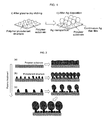
- Inventors have also found a method for producing a substrate for surface-enhanced Raman spectroscopy which includes forming uniform protuberant structures having protruded curved surface on a polymer substrate using plasma dry etching, and depositing a metal using vapor deposition to provide a substrate for surface-enhanced Raman spectroscopy having metal nanoparticles distanced several nanometers apart on the metal.
- a substrate for surface-enhanced Raman spectroscopy includes metal nanoparticles which are uniformly spaced several nanometers apart with each other on the surface in a large scale, allows surface-enhanced Raman signals to be notably improved, even in cases of long-term storage, and allows quantitative analysis due to reproducible enhancement effects.
- a method for producing a substrate for surface-enhanced Raman spectroscopy produces at a large scale with simple equipment and at a low production cost and reproducibly produces the distance between the metal nanoparticles to be several nanometers.
- a Raman spectroscopic device includes a light source; the substrate for surface-enhanced Raman spectroscopy described above; and a detector configured to detect Raman spectrum.
- a method for detecting Raman spectroscopy of an analyte includes: preparing the substrate for surface-enhanced Raman spectroscopy described above; approaching or contacting an analyte to the substrate; irradiating the analyte; and detecting scattered Raman signals of the analyte.
- a substrate for surface-enhanced Raman spectroscopy may include a polymer substrate of which protuberant structures having an upper protruded curved surface are formed to be spaced-apart on a first surface; metal-containing nanoparticles formed on the protuberant structures; and a metal-containing thin layer formed on a part or the entire part of the first surface of the polymer substrate where the protuberant structures are not formed, wherein the metal-containing nanoparticle forms a nanogap with an adjacent metal-containing nanoparticle, an adjacent metal-containing thin layer or both to create a surface plasmon resonance during irradiating a light.
- a Raman spectroscopic device may include a light source; the substrate for surface-enhanced Raman spectroscopy described above; and a detector configured to detect Raman spectrum.
- the light source may a laser which can provide a high energy incident light.
- a method for detecting Raman spectroscopy of an analyte may include: preparing a substrate for surface-enhanced Raman spectroscopy; approaching or contacting an analyte to the substrate; irradiating the analyte; and detecting scattered Raman signals of the analyte.
- a term “surface-enhanced Raman spectroscopy (SERS)” may be also called as surface-enhanced Raman scattering.
- the surface-enhanced Raman spectroscopy determines Raman scattering signal enhanced of a material to be analyzed which is adsorbed on or present within a distance of several hundred nanometers from a roughen surface of a Raman active material, for example, such as a metal.
- the intensity of enhanced signal can be higher 10 4 to 10 6 than that of conventional Raman signal, as being due to a surface plasmon provided by the roughening of the surface.
- General Raman scattering which is an inelastic photon scattering phenomenon, can occur with a change in energy of a molecule due to a vibrational transition to another energy level when light encounters the molecule.
- the Raman spectroscopy can detect signals of a nonpolar molecule having a change in induced polarizability and can be suitable for detecting biomolecules, for example, such as proteins, genes and the like since almost all of organic molecules have specific Raman shifts (cm -1 ) and are not affected by interference of water molecules.
- wavelengths of Raman emission spectrum provide chemical composition and structural properties of a light absorbed molecule, it can be used to directly analyze an analyte using the Raman signals.
- Raman spectroscopy has not been commercialized since a high-performance device is required to detect week signals of Raman spectroscopy.
- the electromagnetic effect is dominant.
- the electromagnetic enhancement is dependent on the presence of the metal surface's roughness features.
- the surface-enhanced Raman signals are observed primarily for an analyte adsorbed onto the surface of a coinage metal, for example, such as Au, Ag, Cu or an alkali metal, for example, such as Li, Na, K, with the excitation wavelength near or in the visible region.
- the intensity of the Raman signal is proportional to the square of the magnitude of any electromagnetic field incident on an analyte and the electromagnetic field is sum of the electromagnetic field applied to the analyte in the absence of metal roughness features and the electromagnetic field resulted from the particulate metal roughness features.
- the inventor of this disclosure are to provide a substrate for surface-enhanced Raman spectroscopy which includes nanogaps uniformly distributed in a large scale.
- the substrate for surface-enhanced Raman spectroscopy is prepared by forming metal-containing nanoparticles on protuberant structures by depositing a metal, which is a Raman active material, on a polymer substrate through a vapor deposition and forming a metal-containing thin layer formed on a part or the entire part of the surface of the polymer substrate where the protuberant structures are not formed.
- the size of the metal nanoparticles is controlled by controlling metal vapor deposition according to the distance between the protuberant structures to arrange the metal nanoparticles in constant intervals of several nanometers.
- a term "surface Plasmon resonance (SPR)" is the collective oscillation of conduction electrons at the interface between a negative and positive permittivity material stimulated by incident light. The resonance condition is established when the frequency of incident photons matches the natural frequency of surface electrons oscillating against the restoring force of positive nuclei. Particularly, the surface Plasmon resonance resulting the confinement of a surface plasmon in a nanoparticle of size is called as a localized surface plasmon resonance.
- a material adsorbed on a metal surface for example, such as Au or Ag, can be analyzed using the surface plasmon resonance.
- a substrate for surface-enhanced Raman spectroscopy may include metal nanoparticles, particularly circular or oval metal nanoparticles, on protuberant structures of a polymer substrate, and a metal-containing thin layer formed on a part or the entire part of the surface of the polymer substrate where the protuberant structures are not formed.
- the substrate for surface-enhanced Raman spectroscopy may provide synergistic signal-enhanced effects to sensitively detect Raman signals due to the surface plasmon resonance between nanoparticles which are spaced several nanometers apart with each other on the protuberant structures, and the surface plasmon formed by the metal-containing thin layer formed on the part of the surface of the polymer substrate where the protuberant structures are not formed and formed a few tens of nanometers away from the nanoparticles.
- the metal When a metal is deposited on the polymer substrate including protuberant structures through sputtering, the metal may be first deposited uniformly on the protuberant structures and the space between the protuberant structures.
- the metal may be intensively deposited on the protuberant structures as the deposition is progressed due to shadow effect caused by the sputtered particles. Because the surface, where the protuberant structures are not formed, may be blocked by adjacent protuberant structures and spherically growing nanoparticles on the structures, an amount of the metal which reaches to the surface may be significantly reduced.
- the metal ions may be intensively deposited to form and grow nanoparticles on the protuberant structures where the negative charges are accumulated.
- This metal deposition on the protuberant structures of the polymer substrate may form not a continuous film but independent spherical nanoparticles.
- the metal particles may not be uniformly deposited on the protuberant structures due to negative charges selectively accumulated on the protuberant structures, poor bond between the polymer and the metal, and high curvature of a upper part of the protuberant structures.
- the metal particles may not be grown on the side surfaces of the structures due to poor bond between the polymer and the metal and low wettability.
- the protuberant structures may be spaced-apart in constant intervals to provide the substrate having the structural features described above.
- the protuberant structures may be spaced-apart in constant intervals of 10 to 500 nm, preferably in constant intervals of 20 to 200 nm, and more preferably in constant intervals of 40 to 80 nm.
- the metal nanoparticles to be formed on the protuberant structures may not be formed as independent particles which are spaced-apart in a distance of several nanometers but may be formed as a continuous film.
- the metal-containing thin layer may be thickly formed since the portion where the shadow effect can be applied becomes broad. Therefore, the boundaries between the portion and nanoparticles formed on the protuberant structures may be blurred.
- the size of the nanoparticles may become bigger to maintain the gaps between nanoparticles in a nanometer level.
- the density of the nanogaps per unit area may be also reduced and the number of spots may be thus decreased to enhance Raman signals.
- the protuberant structures may include the protruded curved surface.
- An etching method may be thus used rather than an imprinting method which provides flat and angled structures.
- the protuberant structure may be formed by dry etching the surface of the polymer substrate.
- the dry etching may be a plasma dry etching performed by using at least one gas chosen from argon, oxygen, hydrogen, helium and nitrogen gas.
- the plasma dry etching of the polymer substrate may be carried by various methods known in the art.
- the plasma dry etching may be performed to the polymer substrate to form protrusions. Space and size of the protrusions may be controlled by changing various factors, for example, such as flow rate of the gas and power that forms plasma, exposure time to the plasma and the like.
- the metal-containing nanoparticles and the metal-containing thin layer may be formed by a vapor deposition of the first surface of the polymer substrate on which protuberant structures having protruded curved surface are formed to be spaced-apart.
- the vapor deposition may be performed by sputtering, evaporation and chemical vapor deposition. However, it is not limited thereto.
- the metal-containing nanoparticles on the protuberant structures may be formed in a spherical or oval shape. However, the shape of the metal-containing nanoparticle is not limited thereto.
- the metal-containing nanoparticles may have an average particle size of 5 nm to 1 ⁇ m.
- the metal-containing nanoparticles may have an average particle size of 10 nm to 300 nm. However, the size of metal-containing nanoparticles may not be limited thereto.
- a horizontal maximum width W1 of the metal-containing nanoparticles which are formed vertically to the polymer substrate may equal to or greater than a horizontal maximum width W2 of the protuberant structure which is formed vertically to the polymer substrate, and less than the shortest distance W3 between centers of the protuberant structures.
- a horizontal maximum width W1 of the metal-containing nanoparticles is less than the horizontal maximum width W2 of the protuberant structure, enhancement of Raman effects may not be provided.
- the size is less than that of the protuberant structure which does not show enhancement of Raman effects, efficient enhancement of Raman effect may not be provided since the distance between the nanoparticles increases.
- nanogaps which provide significant enhancement of Raman signals may not be formed, but an embossed surface having unevenness of a continuous curved surface may be formed.
- nanogaps of the surface-enhanced Raman spectroscopy may be formed in a range of 1 to 10 nm which may be controlled by the distance between the metal-containing nanoparticles.
- the distance between the metal-containing nanoparticles may be controlled by adjusting the distance between the protuberant structures and size of the metal-containing nanoparticles formed on the protuberant structures.
- the metal-containing nanoparticles may be nanoparticles including a Raman active material, for example, such as a metal, a metal oxide and a metal nitride.
- the metal of the metal-containing nanoparticles may be chosen from Au, Ag, Cu, Pt and Pd, and an alloy thereof to enhance of Raman signals of an analyte adsorbed on the metal by providing the electromagnetic field enhance by the surface Plasmon resonance.
- the polymer substrate may be formed of a polymer chosen from acrylic polymer, polyethersulfone (PES), polycycloolefin (PCO), polyiourethane and polycarbonate (PC) to provide uniformly arranged protuberant structures on the substrate through the plasma dry etching.
- the polymer substrate may be also formed by forming a reinforced coating layer including the polymer on another substrate.
- the polymer substrate may be a substrate formed of an acrylic polymer itself or a substrate on which a reinforced coating layer including an acrylic polymer is formed.
- acrylic polymer may be poly(methyl methacrylate) (PMMA), polymethacrylate, poly(methyl acrylate)(PMA), poly(ethyl acrylate)(PEA), poly(2-chloroethyl vinyl ether)(PCVE), poly(2-ethylhexyl acrylate)(PEHA), poly(hydroxyethyl methacrylate)(PHEMA), poly(butyl acrylate)(PBA), poly(butyl methacrylate)(PBMA), polyethylene terephthalate(PET), polyethylene naphthalate(PEN) and poly(trimethylolpropane triacrylate)(PTMPTA).
- PMMA poly(methyl methacrylate)
- PMA poly(methyl acrylate)
- PEA poly(ethyl acrylate)
- PCVE poly(2-chloroethyl vinyl ether)
- PCVE poly(2-ethylhexyl acrylate)(PEHA)
- PHEMA poly(
- the reinforced coating layer may include a polymer coating material chosen from an acrylic coating material, a poly urethane-based coating material, an epoxy-based coating material, and primer-based coating material.
- the reinforced coating layer may further include inorganic fine particles chosen from a metal oxide, a metal sulfide, alumina, silica, a zirconium oxide and an iron oxide.
- the reinforced coating layer may be formed in a thickness of 1 to 10 m on a substrate.
- a method for producing a substrate for surface-enhanced Raman spectroscopy may include forming protuberant structures having protruded curved surface to be spaced-apart by dry etching a first surface of a polymer substrate; and forming metal-containing nanoparticles on the protruded curved surfaces of the protuberant structures and a metal-containing thin layer on a part or the entire part of the first surface of the polymer substrate where the protuberant structures are not formed at the same time by a vapor deposition with a metal-containing Raman active material till nanogaps are formed between the metal-containing nanoparticles adjacent with each other.
- the vapor deposition may be performed by sputtering, evaporation and chemical vapor deposition.
- the method for producing a substrate for surface-enhanced Raman spectroscopy can produce a substrate for surface-enhanced Raman spectroscopy at a large scale with simple equipment and at a low production cost.
- the substrate manufactured thereby may allow quantitative analysis due to reproducible enhancement effect.
- the large scale may be 1 mm 2 to 10 m 2 , preferably 1 mm 2 to 1000 cm 2 .
- the scale is not limited thereto.
- An area of the substrate manufactured by the method described herein may vary with the etching method which provides uniformly spaced-apart protuberant structures and the sputtering method which provides uniformly sputtered metal-containing Raman active material. Thus, the area of the substrate may increase as the etching method and the sputtering method are more developed.
- the substrate manufactured by the method described herein may allow notably improved surface-enhanced Raman signals, even in cases of long-term storage, for example, such as several tens of days due to excellent durability. Since the substrate includes metal-containing particles which are distanced several nanometers apart, it may not be easy to cause an oxidation reaction between those narrow spaces even though the substrate is exposed into the atmosphere. When a surface is treated with a metal as a conventional Raman active material, the metal becomes oxidized and Raman signals are thus significantly decreased as the exposure time into the atmosphere increases. However, the substrate according to an example may still maintain the improved Raman signals at a high level.
- the substrate according to an example shows improved Raman signals at a very constant level in a Raman map with 32 pixel x 32 pixel resolution for an area of 10 ⁇ m x 10 ⁇ m. It is also noted in FIG. 7 that the reproducibility is within a deviation of about 6% after the same experiment is repeated more than 300 times. It is further noted in FIG. 8 that when the substrate is stored for more than 40 days, the improved Raman signals are sustained at the same level, compared to the level when the immediately prepared substrate shows.
- a Raman spectroscopic device may include a light source; the substrate for surface-enhanced Raman spectroscopy described above; and a detector configured to detect Raman spectrum.
- the Raman effects of Raman spectroscopy is very week.
- a Raman spectroscopic device equipped with the substrate for surface-enhanced Raman spectroscopy may be provided in order to resolve this problem.
- the light source may be a laser which can provide high dense photons.
- the detector may include a photomultiplier tube (PMT), an avalanche photodiode (APD), a charge coupled device (CCD) and the like to efficiently amplify signals.
- PMT photomultiplier tube
- APD avalanche photodiode
- CCD charge coupled device
- a method for detecting Raman spectroscopy of an analyte may include: preparing the substrate for surface-enhanced Raman spectroscopy described above; approaching or contacting an analyte to the substrate; irradiating the analyte; and detecting scattered Raman signals of the analyte.
- the substrate for surface-enhanced Raman spectroscopy including metal nanoparticles which are spaced several nanometers apart on a substrate can be manufactured at a large scale with simple equipment and at a low production cost. Additionally, as the distance between the metal nanoparticles can be reproducibly produced to be several nanometers, the Raman signals can be notably improved, and even in the case of long-term storage, the improved Raman signals can be sustained at a high level.
- Example 1 Preparation of a substrate for surface-enhanced Raman spectroscopy including nanogaps and Property analysis
- Step 1 Forming protuberant structures by plasma dry etching
- a dry etching was performed on a polymer substrate formed of polyethylene terephthalate having a thickness of 188 ⁇ m which was purchased from Panac Co. using a 13.56 MHz capacitively coupled plasma-typed power supply.
- An etching system was composed of a shower head part with a diameter of 6 in. including an annular stainless steel tube with a diameter of 0.23 in. and an electrode with a diameter of 6 in. formed on the upper part which is 15 cm apart from the shower head part.
- the polymer substrate with a thickness of 125 ⁇ m purchased from Panac Co. was attached to the electrode.
- a 99.999% Argon gas was supplied to a reactor through the shower head at a flow rate of 50 sccm to increase a pressure of a reaction chamber to 22.7 Pa when the pressure of the reaction chamber was reached to a vacuum level of 6.7 Pa.
- the plasma dry etching was performed at a RF power of 200W which is 1.1 W/cm2 by changing etching time.
- a plasma ion energy applied from self-bias to the polymer substrate was 102 eV during the etching process.
- a temperature of the polymer substrate was kept at 50°C or lower during the etching process.
- a distance of nanometer scale between protuberant structures formed on the polymer substrate was linearly increased as the etching time increases.
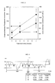
- the distance between protuberant structures was in a range of 40 to 80 nm (see FIG. 3 ).
- the distance between and the size of the protuberant structure were determined using AFM cross-section profile.
- Step 2 Deposition of a metal-containing Raman active material
- Ag particles of a Raman active material were deposited on the surface including the protuberant structures of the polymer substrate prepared in Step 1 using a sputtering vapor deposition method.
- the deposition was performed using a magnetron multi-gun sputtering system (A-Tech System Co., Ltd., Flexlab system 100) at room temperature.
- the polymer substrate, on which the protuberant structures were formed using the plasma dry etching method in Step 1 was mounted at a substrate holder which is positioned at the upper 15 cm of an Ag sputtering target in the sputtering system.
- Argon gas was supplied at a flow rate of 45 sccm to increase the pressure to 3 mTorr.
- Ag particles were deposited by DC reactive sputtering using Ag target with a diameter of 4 in. (Williams Advanced Materials Inc.) and a DC power of 0.13 W/cm 2 .
- Ar plasma pretreatment was performed on the polymer protuberant structures for 60 seconds under RF 200W to form Ag nanoparticles with a size of 60nm and a thin film on the substrate on which the protuberant structures are not formed by sputtering.
- a substrate for surface-enhanced Raman spectroscopy was prepared by forming protuberant structures on a polymer, for example, such as PC, PEN and PET substrates and then depositing Ag nanoparticles as described above.
- FIG. 4 is a graph illustrating the distance and the height.
- the Ag nanoparticles formed on the protuberant structures have gaps of several nanometers between each other.
- the average height between the top part of the Ag nanoparticles and the substrate surface on which the Ag thin film is formed but the protuberant structures are not formed is about 10 nm to provide additional enhanced Raman signals.
- Optimizing Raman signal enhancement by controlling the distance between the nanoparticles can be achieved by not only controlling time and conditions of the plasma dry etching in Step 1 to control size and distance of the protuberant structures but also controlling time and conditions of the sputtering in Step 2 to control size of the nanoparticles.
- Example 2 Optical properties of the substrate for surface-enhanced Raman spectroscopy
- Optical properties of the substrate for surface-enhanced Raman spectroscopy including the metal nanoparticles on the PET polymer substrate prepared in Example 1 were determined.
- the distance between metal nanoparticles of the substrate for surface-enhanced Raman spectroscopy was controlled to be in a range of several nanometers by controlling the distance between the protuberant structures in Step 1 and the size of the metal nanoparticles in Step 2.
- the metal nanoparticles showed high absorbance at a specific wavelength region for an incident light. A position of the maximum absorption wavelength was changed depending on size of the nanoparticles.
- the optical properties contribute to properties of the surface-enhanced Raman spectroscopy.
- Example 3 Detection of Raman signals from the substrate for surface-enhanced Raman spectroscopy
- Enhancement effect of the substrate for surface-enhanced Raman spectroscopy prepared in Example 1 was determined on Raman signals of an analyte using benzenethiol as a sample. 2 M benzenethiol solution 100 ⁇ l was dropped on 2.5 cm x 1.3 cm size of the substrate for surface-enhanced Raman spectroscopy and dried for 1 hour. The substrate for surface-enhanced Raman spectroscopy on which benzenethiol was adsorbed was rinsed with ethanol several times and dried with N 2 .
- Raman signals of an analyte was determined at a 10 ⁇ m x 10 ⁇ m region of the substrate for surface-enhanced Raman spectroscopy on which the analyte was adsorbed.
- a 532 nm wavelength laser of 0.2 mW was used to irradiate.
- a 10 ⁇ m x 10 ⁇ m area was divided into 32 pixel x 32 pixel for a point to obtain a spectrum to be a diffraction limit and exposed for 2 seconds to provide Raman spectrum.
- An enhancement factor (EF) was provided by converting a peak area shown at the 998 cm -1 region of benzenethiol for Raman mapping. EF values were mapped in the 10 ⁇ m x 10 ⁇ m region. A part thereof was enlarged and EF values determined at each pixel was shown in FIG. 6 .
- Raman signals were determined at the 10 ⁇ m x 10 ⁇ m region, total 32x32 which is 1024 pixels and the EF values converted therefrom were distributed in a 1.1 to 1.4x10 7 region. It was shown normal distribution (Gaussian) with narrow FWHM (full-width half maximum) of about 0.1x10 7 which showed maximum distribution at about 1.25x10 7 and also relatively even EF values at a large area. It is noted that when the substrate for surface-enhanced Raman spectroscopy according to an example is used, signal enhancement effects are exhibited in a large area so that it can be suitable for both qualitative analysis and quantitative analysis.
- Raman mapping experiments were performed more than 350 times to determine reproducibility of Raman signals using the substrate for surface-enhanced Raman spectroscopy according to an example and statistical EF values were determined. Those EF values were distributed in a similar region to the 1.1 to 1.7x10 7 region where EF values were distributed in the single mapping and showed maximum distribution at about 1.3x10 7 . FWHM distribution was obtained from each mapping. It is noted that the FWHM from each mapping shows 0 to 25% to the average value obtained from the single mapping and the maximum distribution shows 10 to 15% to the average value obtained from the single mapping. The reproducibility experiments were performed using samples prepared from 5 batches to show that signal enhancement can be reproducibly provided in the substrates produced by same manufacturing process.
- the substrate for surface-enhanced Raman spectroscopy according to an example uniformly enhances Raman signals over a large area and allows reproducible enhancement even after repeating hundreds of times. Thus, it can be suitable for both qualitative analysis and quantitative analysis.
- Example 4 Stability of the substrate for surface-enhanced Raman spectroscopy
- a stability test on exposure to air was performed to commercialize the substrate for surface-enhanced Raman spectroscopy according to an example.
- Statistical EF values were provided after Raman mapping more than 350 times at each point and then plotted as a function of storage time.
- the substrate was exposed to the air with a temperature of 22°C and a humidity of 40%. The result is shown in FIG. 8 .
- the substrate for surface-enhanced Raman spectroscopy which is prepared by vapor depositing a Raman active metal on the polymer substrate, on which the protuberant structures are uniformly formed, to arrange nanoparticles to have nanogaps by controlling the size of and the distance between the nanoparticles on protuberant structures, can be manufactured at a large scale with simple equipment and at a low production cost since the manufacturing method is simple and does not require cost equipments.
- the substrate for surface-enhanced Raman spectroscopy can be uniformly formed at large scale production to be suitable for mass production.
- the Raman signals can be notably improved, and even in the case of long-term storage, the improved Raman signals can be sustained at a high level. It can be thus suitable for both qualitative analysis and quantitative analysis and can be commercialized.
Landscapes
- Chemical & Material Sciences (AREA)
- Health & Medical Sciences (AREA)
- Life Sciences & Earth Sciences (AREA)
- Physics & Mathematics (AREA)
- Immunology (AREA)
- Engineering & Computer Science (AREA)
- General Physics & Mathematics (AREA)
- Pathology (AREA)
- General Health & Medical Sciences (AREA)
- Biochemistry (AREA)
- Analytical Chemistry (AREA)
- Nuclear Medicine, Radiotherapy & Molecular Imaging (AREA)
- Organic Chemistry (AREA)
- Materials Engineering (AREA)
- Spectroscopy & Molecular Physics (AREA)
- Biomedical Technology (AREA)
- Urology & Nephrology (AREA)
- Hematology (AREA)
- Wood Science & Technology (AREA)
- Inorganic Chemistry (AREA)
- Molecular Biology (AREA)
- Mechanical Engineering (AREA)
- General Chemical & Material Sciences (AREA)
- Chemical Kinetics & Catalysis (AREA)
- Metallurgy (AREA)
- Microbiology (AREA)
- Medicinal Chemistry (AREA)
- Food Science & Technology (AREA)
- Biotechnology (AREA)
- Cell Biology (AREA)
- Investigating, Analyzing Materials By Fluorescence Or Luminescence (AREA)
Abstract
Description
- This application claims the benefit under 35 USC § 119(a) of Korean Patent Application No.
10-2013-0112087 filed on September 17, 2013 - The following description relates to a substrate for surface-enhanced Raman spectroscopy allowing Surface-enhanced Raman spectroscopic signals to be notably improved, even in cases of long-term storage, by producing the substrate so that metal nanoparticles thereon are distanced several nanometers apart, and to a method for producing a substrate for surface-enhanced Raman spectroscopy at a large scale with simple equipment and at a low production cost.
- Raman scattering or the Raman Effect is an inelastic photon scattering phenomenon. When photons are scattered from an atom or molecule, most photons are elastically scattered (Rayleigh scattering), such that the scattered photons have the same energy (frequency and wavelength) as the incident photons. A small fraction of the scattered photons (approximately 1 in 10 million) are scattered by an excitation, with the scattered photons having a frequency different from, and usually lower than, that of the incident photons. In a gas, Raman scattering can occur with a change in energy of a molecule due to a transition to another (usually higher) energy level.
- Raman Effect (Raman shift) is exhibited in almost organic molecules including not only by polar molecules but also by non-polar molecules which have induction polarizability when Raman spectroscopy using Raman scattering is applied. It is thus more suitable for the detection of biomolecules such as proteins, genes and the like since it is not affected by interference caused by water molecules.
- On the other hand, specific wavelengths of Raman emission spectrum represents chemical composition and structure features so that it can be used to directly analyze materials using Raman signals.
- Even though an analyte can be analyzed directly, it has not been practically used, except to academic researches, because it requires costly equipments to detect very week signals and has very low reproducibility of signals. In order to overcome such drawbacks, in 1974, Fleischmann et al. reported enhancements of Raman signals of pyridine adsorbed on a silver electrode roughened by successive oxidation-reduction cycles. The signals were 106 higher than expected, and they were originally explained as being due to the additional surface area provided by the roughening of the surface. That is, the surface-enhanced Raman spectroscopy is a phenomenon showing enhancements of Raman signals of a targeted molecule when the molecule is present around the metallic nanostructure.
- Analysis using the surface-enhanced Raman scattering provides information which can be difficult to obtain through a typical Raman analysis. It is needed to study how a material to be analyzed interacts with a surface in order to determine whether a surface-enhanced Raman scattering analysis is possible. Since various surface interactions are involved between a material to be analyzed and the surface of a metal, enhanced Raman signals, which cannot be provided by a typical Raman analysis, are adsorbed. The surface-enhanced Raman scattering may occur when a material to be analyzed is adsorbed or close to a metallic surface. Coherent free electron oscillations that exist at the interface between a metal and incident light must occur to efficiently enhance Raman emission. This is called as a surface plasmon which provides electromagnetic enhancement. The incident light creates surface plasmons (electromagnetic effect) on a metal surface which enhance Raman emission through interaction (charge-transfer effect) with an analyte.
- Roughness of the surface of a substrate on which an analyte is placed roles an important factor for occurrence of surface plasmons and enormous enhancement of Raman signals therefrom. Thus, various studies using nanotechnologies have been developed to roughen the surface of a substrate to provide nanostructures such as nanometer-sized columns, linear broken surface or nanoparticles.
- Generally, optical, electrical, physical and chemical properties of a metallic nano material can be controlled by changing its size, shape, crystalline structure and the like. Precious metal nanoparticles composed of Au or Ag strongly resonate with light in the visible region to yield strong absorption and scattering.
- A surface plasmon resonance frequency varies with various factors, for example, such as kind, for example, such as Au, Ag, Cu, Pt, Pd and the like, size, and shape of metal nanoparticles, a solvent into which metal nanoparticles are dispersed, a kind of laser (incident light) and the like. Thus, surface-enhanced Raman signals can be obtained by controlling these factors.
- Surface-enhanced Raman scattering is a technique to analyze a trace amount of a material by enhancing Raman signals through surface Plasmon resonance on a metal surface including nanometer-sized structures, for example, such as metal particles or patterns. Reproducibility of signals should be resolved to commercialize the surface-enhanced Raman scattering technique. Producing Raman probes should be also resolved through structural control of nanoparticles or patterns to commercialize the surface-enhanced Raman scattering technique. However, there is still limit to reproducibly produce enhanced Raman signals at a large scale. One approach to resolve those problems is patterning a substrate for surface-enhanced Raman spectroscopy in a large scale. This approach includes a top-down method, for example, such as an e-beam lithography and a focused ion beam milling, and a bottom-up method, for example, such as patterning using a mold and a colloidal lithography.
- The bottom-up method allows massive parallel processing and rapid production of patterned nanostructures economically at a large scale. On the other hand, the top-down method allows excellent control of size and shape of particles, but requires high production cost and has limitation in implementing at a large scale.
- However, since the surface-enhanced Raman scattering technology can detect even with a trace amount of an analyte at a low intensity, much attention has been given to their study in a biosensor application field. The surface-enhanced Raman scattering technology can provide information on the chemical structure of an analyte in a narrow spectrum and allow multiple detections since each molecule has its own unique Raman signal unlike existing fluorescence analysis. Thus, a great deal of development research is currently under way on detections of bio materials (DNAs, proteins, cells, etc.) and disease diagnosis devices utilizing the surface-enhanced Raman scattering technology. In addition, surface-enhanced Raman diagnosis devices having continuous reproducibility can be implemented using microfluidic devices and Raman spectroscopic technique.
- Accordingly, inventors of this following description have found a substrate for surface-enhanced Raman spectroscopy which allows surface-enhanced Raman signals to be notably improved, even in cases of long-term storage, by producing the substrate so that metal nanoparticles thereon are distanced several nanometers apart, and a method for producing the substrate for surface-enhanced Raman spectroscopy at a large scale with simple equipment and at a low production cost. Inventors have also found a method for producing a substrate for surface-enhanced Raman spectroscopy which includes forming uniform protuberant structures having protruded curved surface on a polymer substrate using plasma dry etching, and depositing a metal using vapor deposition to provide a substrate for surface-enhanced Raman spectroscopy having metal nanoparticles distanced several nanometers apart on the metal.
- This Summary is provided to introduce a selection of concepts in a simplified form that are further described below in the Detailed Description. This Summary is not intended to identify key features or essential features of the claimed subject matter, nor is it intended to be used as an aid in determining the scope of the claimed subject matter.
- According to one general aspect, a substrate for surface-enhanced Raman spectroscopy includes metal nanoparticles which are uniformly spaced several nanometers apart with each other on the surface in a large scale, allows surface-enhanced Raman signals to be notably improved, even in cases of long-term storage, and allows quantitative analysis due to reproducible enhancement effects.
- According to another general aspect, a method for producing a substrate for surface-enhanced Raman spectroscopy produces at a large scale with simple equipment and at a low production cost and reproducibly produces the distance between the metal nanoparticles to be several nanometers.
- According to another general aspect, a Raman spectroscopic device includes a light source; the substrate for surface-enhanced Raman spectroscopy described above; and a detector configured to detect Raman spectrum.
- According to another general aspect, a method for detecting Raman spectroscopy of an analyte includes: preparing the substrate for surface-enhanced Raman spectroscopy described above; approaching or contacting an analyte to the substrate; irradiating the analyte; and detecting scattered Raman signals of the analyte.
- A substrate for surface-enhanced Raman spectroscopy according to an example may include a polymer substrate of which protuberant structures having an upper protruded curved surface are formed to be spaced-apart on a first surface; metal-containing nanoparticles formed on the protuberant structures; and a metal-containing thin layer formed on a part or the entire part of the first surface of the polymer substrate where the protuberant structures are not formed, wherein the metal-containing nanoparticle forms a nanogap with an adjacent metal-containing nanoparticle, an adjacent metal-containing thin layer or both to create a surface plasmon resonance during irradiating a light.
- A Raman spectroscopic device may include a light source; the substrate for surface-enhanced Raman spectroscopy described above; and a detector configured to detect Raman spectrum. The light source may a laser which can provide a high energy incident light.
- A method for detecting Raman spectroscopy of an analyte may include: preparing a substrate for surface-enhanced Raman spectroscopy; approaching or contacting an analyte to the substrate; irradiating the analyte; and detecting scattered Raman signals of the analyte.
-
-
FIG. 1 is diagrams illustrating an example of a substrate for surface-enhanced Raman spectroscopy and an example of a method for manufacturing the same. -
FIG. 2 is diagrams illustrating examples of structures formed by a metal deposition depending on a presence and a distance of protuberant structures on a polymer substrate. -
FIG. 3 is a graph illustrating height of and distance between protuberant structures on an example of a substrate depending on plasma treatment time. -
FIG. 4 is a graph illustrating a depth profile of an Atomic Force Microscopic image and a sectioned surface for the surface of an example of a substrate for surface-enhanced Raman spectroscopy. -
FIG. 5 is a graph illustrating absorbance according to size of metal nanoparticles formed on protuberant structures on a polymer substrate by a vapor deposition. -
FIG. 6 is a distribution graph illustrating estimated EF values at each pixel based on a Raman mapping using an example of a substrate for surface-enhanced Raman spectroscopy. -
FIG. 7 is a graph illustrating uniformly enhanced Raman signal at a large scale of an example of a substrate for surface-enhanced Raman spectroscopy. FW-HM distributions and center values of each experiment obtained by Gaussian fitting of the EF distributions which are estimated for an area of 10 µm x 10 µm after performing more than 300 times are plotted. -
FIG. 8 is a diagram illustrating stability of an example of a substrate for surface-enhanced Raman spectroscopy after exposed to air. Statistical EF values are obtained by performing Raman mappings more than 350 times at each point and the result is shown as a function of storage time. The substrate is exposed to air with temperature of 22°C and humidity of 40%. - The following detailed description is provided to assist the reader in gaining a comprehensive understanding of the methods, apparatuses, and/or systems described herein. However, various changes, modifications, and equivalents of the methods, apparatuses, and/or systems described herein will be apparent to one of ordinary skill in the art. The sequences of operations described herein are merely examples, and are not limited to those set forth herein, but may be changed as will be apparent to one of ordinary skill in the art, with the exception of operations necessarily occurring in a certain order. Also, descriptions of functions and constructions that are well known to one of ordinary skill in the art may be omitted for increased clarity and conciseness.
- Throughout the description of the present disclosure, a term "surface-enhanced Raman spectroscopy (SERS)" may be also called as surface-enhanced Raman scattering. The surface-enhanced Raman spectroscopy determines Raman scattering signal enhanced of a material to be analyzed which is adsorbed on or present within a distance of several hundred nanometers from a roughen surface of a Raman active material, for example, such as a metal. The intensity of enhanced signal can be higher 104 to 106 than that of conventional Raman signal, as being due to a surface plasmon provided by the roughening of the surface.
- General Raman scattering, which is an inelastic photon scattering phenomenon, can occur with a change in energy of a molecule due to a vibrational transition to another energy level when light encounters the molecule. Unlike infrared spectroscopy which measures vibrational energy to cause a change in dipole moment and is thus widely used to analyze the vibrational transition, the Raman spectroscopy can detect signals of a nonpolar molecule having a change in induced polarizability and can be suitable for detecting biomolecules, for example, such as proteins, genes and the like since almost all of organic molecules have specific Raman shifts (cm-1) and are not affected by interference of water molecules. Since wavelengths of Raman emission spectrum provide chemical composition and structural properties of a light absorbed molecule, it can be used to directly analyze an analyte using the Raman signals. However, despite this availability, Raman spectroscopy has not been commercialized since a high-performance device is required to detect week signals of Raman spectroscopy.
- Various methods have been developed to enhance the Raman signals. There are two primary mechanisms of enhancement, an electromagnetic and a chemical enhancement. The electromagnetic effect is dominant. The electromagnetic enhancement is dependent on the presence of the metal surface's roughness features. The surface-enhanced Raman signals are observed primarily for an analyte adsorbed onto the surface of a coinage metal, for example, such as Au, Ag, Cu or an alkali metal, for example, such as Li, Na, K, with the excitation wavelength near or in the visible region. The intensity of the Raman signal is proportional to the square of the magnitude of any electromagnetic field incident on an analyte and the electromagnetic field is sum of the electromagnetic field applied to the analyte in the absence of metal roughness features and the electromagnetic field resulted from the particulate metal roughness features. There are efforts to manufacture a substrate, which can provide surface-enhanced Raman signals significantly enhanced to a high level by controlling surface structure, particularly roughness, in various fields. Nat. Nanotechnology, 2010, 5(10): 732-736; Chin. Phys. Lett., 2007, 24(10): 2934-2937 reported significantly enhanced Raman signals on a structure including several nanometers of gaps. Accordingly, the inventor of this disclosure are to provide a substrate for surface-enhanced Raman spectroscopy which includes nanogaps uniformly distributed in a large scale. The substrate for surface-enhanced Raman spectroscopy is prepared by forming metal-containing nanoparticles on protuberant structures by depositing a metal, which is a Raman active material, on a polymer substrate through a vapor deposition and forming a metal-containing thin layer formed on a part or the entire part of the surface of the polymer substrate where the protuberant structures are not formed. Here, the size of the metal nanoparticles is controlled by controlling metal vapor deposition according to the distance between the protuberant structures to arrange the metal nanoparticles in constant intervals of several nanometers.
- Throughout the description of the present disclosure, a term "surface Plasmon resonance (SPR)" is the collective oscillation of conduction electrons at the interface between a negative and positive permittivity material stimulated by incident light. The resonance condition is established when the frequency of incident photons matches the natural frequency of surface electrons oscillating against the restoring force of positive nuclei. Particularly, the surface Plasmon resonance resulting the confinement of a surface plasmon in a nanoparticle of size is called as a localized surface plasmon resonance. A material adsorbed on a metal surface, for example, such as Au or Ag, can be analyzed using the surface plasmon resonance.
- A substrate for surface-enhanced Raman spectroscopy according to an example may include metal nanoparticles, particularly circular or oval metal nanoparticles, on protuberant structures of a polymer substrate, and a metal-containing thin layer formed on a part or the entire part of the surface of the polymer substrate where the protuberant structures are not formed. The substrate for surface-enhanced Raman spectroscopy may provide synergistic signal-enhanced effects to sensitively detect Raman signals due to the surface plasmon resonance between nanoparticles which are spaced several nanometers apart with each other on the protuberant structures, and the surface plasmon formed by the metal-containing thin layer formed on the part of the surface of the polymer substrate where the protuberant structures are not formed and formed a few tens of nanometers away from the nanoparticles. When a metal is deposited on the polymer substrate including protuberant structures through sputtering, the metal may be first deposited uniformly on the protuberant structures and the space between the protuberant structures. However, the metal may be intensively deposited on the protuberant structures as the deposition is progressed due to shadow effect caused by the sputtered particles. Because the surface, where the protuberant structures are not formed, may be blocked by adjacent protuberant structures and spherically growing nanoparticles on the structures, an amount of the metal which reaches to the surface may be significantly reduced.
- When asymmetric accumulation of negative charges is caused on protuberant structures formed on the polymer substrate, it may induce concentration of positive ions or metal ions on protuberant structures. Therefore, the metal ions may be intensively deposited to form and grow nanoparticles on the protuberant structures where the negative charges are accumulated. This metal deposition on the protuberant structures of the polymer substrate may form not a continuous film but independent spherical nanoparticles. The metal particles may not be uniformly deposited on the protuberant structures due to negative charges selectively accumulated on the protuberant structures, poor bond between the polymer and the metal, and high curvature of a upper part of the protuberant structures. The metal particles may not be grown on the side surfaces of the structures due to poor bond between the polymer and the metal and low wettability.
- The protuberant structures may be spaced-apart in constant intervals to provide the substrate having the structural features described above. For example, the protuberant structures may be spaced-apart in constant intervals of 10 to 500 nm, preferably in constant intervals of 20 to 200 nm, and more preferably in constant intervals of 40 to 80 nm. When the distance between the protuberant structures becomes less than 10 nm, the metal nanoparticles to be formed on the protuberant structures may not be formed as independent particles which are spaced-apart in a distance of several nanometers but may be formed as a continuous film. On the other hand, when the distance between the protuberant structures becomes greater than 500 nm, the metal-containing thin layer may be thickly formed since the portion where the shadow effect can be applied becomes broad. Therefore, the boundaries between the portion and nanoparticles formed on the protuberant structures may be blurred. The size of the nanoparticles may become bigger to maintain the gaps between nanoparticles in a nanometer level. The density of the nanogaps per unit area may be also reduced and the number of spots may be thus decreased to enhance Raman signals.
- As described above, the protuberant structures may include the protruded curved surface. An etching method may be thus used rather than an imprinting method which provides flat and angled structures. The protuberant structure may be formed by dry etching the surface of the polymer substrate. The dry etching may be a plasma dry etching performed by using at least one gas chosen from argon, oxygen, hydrogen, helium and nitrogen gas. However, the method is not limited thereto and other method may be used departing from the spirit and scope of the illustrative examples described. The plasma dry etching of the polymer substrate may be carried by various methods known in the art. The plasma dry etching may be performed to the polymer substrate to form protrusions. Space and size of the protrusions may be controlled by changing various factors, for example, such as flow rate of the gas and power that forms plasma, exposure time to the plasma and the like.
- The metal-containing nanoparticles and the metal-containing thin layer may be formed by a vapor deposition of the first surface of the polymer substrate on which protuberant structures having protruded curved surface are formed to be spaced-apart. The vapor deposition may be performed by sputtering, evaporation and chemical vapor deposition. However, it is not limited thereto.
- The metal-containing nanoparticles on the protuberant structures may be formed in a spherical or oval shape. However, the shape of the metal-containing nanoparticle is not limited thereto. The metal-containing nanoparticles may have an average particle size of 5 nm to 1 µm. The metal-containing nanoparticles may have an average particle size of 10 nm to 300 nm. However, the size of metal-containing nanoparticles may not be limited thereto.
- A horizontal maximum width W1 of the metal-containing nanoparticles which are formed vertically to the polymer substrate may equal to or greater than a horizontal maximum width W2 of the protuberant structure which is formed vertically to the polymer substrate, and less than the shortest distance W3 between centers of the protuberant structures. For example, when the horizontal maximum width W1 of the metal-containing nanoparticles is less than the horizontal maximum width W2 of the protuberant structure, enhancement of Raman effects may not be provided. When the size is less than that of the protuberant structure which does not show enhancement of Raman effects, efficient enhancement of Raman effect may not be provided since the distance between the nanoparticles increases. On the other hand, when the horizontal maximum width W1 of the metal-containing nanoparticles is greater than the shortest distance W3 between centers of the protuberant structures, nanogaps which provide significant enhancement of Raman signals may not be formed, but an embossed surface having unevenness of a continuous curved surface may be formed.
- Since the structure with a gap of several nanometers provides significant enhancement of Raman signals, nanogaps of the surface-enhanced Raman spectroscopy may be formed in a range of 1 to 10 nm which may be controlled by the distance between the metal-containing nanoparticles. The distance between the metal-containing nanoparticles may be controlled by adjusting the distance between the protuberant structures and size of the metal-containing nanoparticles formed on the protuberant structures.
- The metal-containing nanoparticles may be nanoparticles including a Raman active material, for example, such as a metal, a metal oxide and a metal nitride. The metal of the metal-containing nanoparticles may be chosen from Au, Ag, Cu, Pt and Pd, and an alloy thereof to enhance of Raman signals of an analyte adsorbed on the metal by providing the electromagnetic field enhance by the surface Plasmon resonance.
- The polymer substrate may be formed of a polymer chosen from acrylic polymer, polyethersulfone (PES), polycycloolefin (PCO), polyiourethane and polycarbonate (PC) to provide uniformly arranged protuberant structures on the substrate through the plasma dry etching. The polymer substrate may be also formed by forming a reinforced coating layer including the polymer on another substrate. Preferably, the polymer substrate may be a substrate formed of an acrylic polymer itself or a substrate on which a reinforced coating layer including an acrylic polymer is formed. Examples of the acrylic polymer may be poly(methyl methacrylate) (PMMA), polymethacrylate, poly(methyl acrylate)(PMA), poly(ethyl acrylate)(PEA), poly(2-chloroethyl vinyl ether)(PCVE), poly(2-ethylhexyl acrylate)(PEHA), poly(hydroxyethyl methacrylate)(PHEMA), poly(butyl acrylate)(PBA), poly(butyl methacrylate)(PBMA), polyethylene terephthalate(PET), polyethylene naphthalate(PEN) and poly(trimethylolpropane triacrylate)(PTMPTA). However, the acrylic polymer is not limited thereto. The reinforced coating layer may include a polymer coating material chosen from an acrylic coating material, a poly urethane-based coating material, an epoxy-based coating material, and primer-based coating material. The reinforced coating layer may further include inorganic fine particles chosen from a metal oxide, a metal sulfide, alumina, silica, a zirconium oxide and an iron oxide. The reinforced coating layer may be formed in a thickness of 1 to 10 m on a substrate.
- A method for producing a substrate for surface-enhanced Raman spectroscopy may include forming protuberant structures having protruded curved surface to be spaced-apart by dry etching a first surface of a polymer substrate; and forming metal-containing nanoparticles on the protruded curved surfaces of the protuberant structures and a metal-containing thin layer on a part or the entire part of the first surface of the polymer substrate where the protuberant structures are not formed at the same time by a vapor deposition with a metal-containing Raman active material till nanogaps are formed between the metal-containing nanoparticles adjacent with each other.
- The vapor deposition may be performed by sputtering, evaporation and chemical vapor deposition.
- The method for producing a substrate for surface-enhanced Raman spectroscopy can produce a substrate for surface-enhanced Raman spectroscopy at a large scale with simple equipment and at a low production cost. The substrate manufactured thereby may allow quantitative analysis due to reproducible enhancement effect. The large scale may be 1 mm2 to 10 m2, preferably 1 mm2 to 1000 cm2. However, the scale is not limited thereto. An area of the substrate manufactured by the method described herein may vary with the etching method which provides uniformly spaced-apart protuberant structures and the sputtering method which provides uniformly sputtered metal-containing Raman active material. Thus, the area of the substrate may increase as the etching method and the sputtering method are more developed.
- The substrate manufactured by the method described herein may allow notably improved surface-enhanced Raman signals, even in cases of long-term storage, for example, such as several tens of days due to excellent durability. Since the substrate includes metal-containing particles which are distanced several nanometers apart, it may not be easy to cause an oxidation reaction between those narrow spaces even though the substrate is exposed into the atmosphere. When a surface is treated with a metal as a conventional Raman active material, the metal becomes oxidized and Raman signals are thus significantly decreased as the exposure time into the atmosphere increases. However, the substrate according to an example may still maintain the improved Raman signals at a high level.
- It is noted in
FIG. 6 that the substrate according to an example shows improved Raman signals at a very constant level in a Raman map with 32 pixel x 32 pixel resolution for an area of 10 µm x 10 µm. It is also noted inFIG. 7 that the reproducibility is within a deviation of about 6% after the same experiment is repeated more than 300 times. It is further noted inFIG. 8 that when the substrate is stored for more than 40 days, the improved Raman signals are sustained at the same level, compared to the level when the immediately prepared substrate shows. - A Raman spectroscopic device according to an example may include a light source; the substrate for surface-enhanced Raman spectroscopy described above; and a detector configured to detect Raman spectrum.
- The Raman effects of Raman spectroscopy is very week. Thus, a Raman spectroscopic device equipped with the substrate for surface-enhanced Raman spectroscopy according to an example may be provided in order to resolve this problem. The light source may be a laser which can provide high dense photons. The detector may include a photomultiplier tube (PMT), an avalanche photodiode (APD), a charge coupled device (CCD) and the like to efficiently amplify signals.
- A method for detecting Raman spectroscopy of an analyte according to an example may include: preparing the substrate for surface-enhanced Raman spectroscopy described above; approaching or contacting an analyte to the substrate; irradiating the analyte; and detecting scattered Raman signals of the analyte.
- The substrate for surface-enhanced Raman spectroscopy including metal nanoparticles which are spaced several nanometers apart on a substrate can be manufactured at a large scale with simple equipment and at a low production cost. Additionally, as the distance between the metal nanoparticles can be reproducibly produced to be several nanometers, the Raman signals can be notably improved, and even in the case of long-term storage, the improved Raman signals can be sustained at a high level.
- Other features and aspects will be apparent from the following detailed description, the drawings, and the claims.
- A dry etching was performed on a polymer substrate formed of polyethylene terephthalate having a thickness of 188 µm which was purchased from Panac Co. using a 13.56 MHz capacitively coupled plasma-typed power supply. An etching system was composed of a shower head part with a diameter of 6 in. including an annular stainless steel tube with a diameter of 0.23 in. and an electrode with a diameter of 6 in. formed on the upper part which is 15 cm apart from the shower head part.
- In particular, the polymer substrate with a thickness of 125 µm purchased from Panac Co. was attached to the electrode. A 99.999% Argon gas was supplied to a reactor through the shower head at a flow rate of 50 sccm to increase a pressure of a reaction chamber to 22.7 Pa when the pressure of the reaction chamber was reached to a vacuum level of 6.7 Pa. The plasma dry etching was performed at a RF power of 200W which is 1.1 W/cm2 by changing etching time. A plasma ion energy applied from self-bias to the polymer substrate was 102 eV during the etching process. A temperature of the polymer substrate was kept at 50°C or lower during the etching process. A distance of nanometer scale between protuberant structures formed on the polymer substrate was linearly increased as the etching time increases. When the etching was processed for 1 min or less under this condition, the distance between protuberant structures was in a range of 40 to 80 nm (see
FIG. 3 ). The distance between and the size of the protuberant structure were determined using AFM cross-section profile. - Ag particles of a Raman active material were deposited on the surface including the protuberant structures of the polymer substrate prepared in
Step 1 using a sputtering vapor deposition method. The deposition was performed using a magnetron multi-gun sputtering system (A-Tech System Co., Ltd., Flexlab system 100) at room temperature. - In particular, the polymer substrate, on which the protuberant structures were formed using the plasma dry etching method in
Step 1, was mounted at a substrate holder which is positioned at the upper 15 cm of an Ag sputtering target in the sputtering system. After a pressure of a deposition chamber was reduced to 4.5 x 10⁻⁶ Torr, 99.999% Argon gas was supplied at a flow rate of 45 sccm to increase the pressure to 3 mTorr. Ag particles were deposited by DC reactive sputtering using Ag target with a diameter of 4 in. (Williams Advanced Materials Inc.) and a DC power of 0.13 W/cm2. Ar plasma pretreatment was performed on the polymer protuberant structures for 60 seconds under RF 200W to form Ag nanoparticles with a size of 60nm and a thin film on the substrate on which the protuberant structures are not formed by sputtering. - As a result, circular or oval Ag nanoparticles were formed on the protuberant structures of the polymer substrate and the thin film was formed on the substrate on which the protuberant structures are not formed.
- A substrate for surface-enhanced Raman spectroscopy was prepared by forming protuberant structures on a polymer, for example, such as PC, PEN and PET substrates and then depositing Ag nanoparticles as described above.
- The polymer surface on which the Ag nanoparticles are formed was scanned using an Atomic Force Microscope to determine distance between the Ag nanoparticles and height between the top part of the Ag nanoparticles and the substrate surface on which the Ag thin film is formed but the protuberant structures are not formed.
FIG. 4 is a graph illustrating the distance and the height. The Ag nanoparticles formed on the protuberant structures have gaps of several nanometers between each other. Moreover, the average height between the top part of the Ag nanoparticles and the substrate surface on which the Ag thin film is formed but the protuberant structures are not formed is about 10 nm to provide additional enhanced Raman signals. - Optimizing Raman signal enhancement by controlling the distance between the nanoparticles can be achieved by not only controlling time and conditions of the plasma dry etching in
Step 1 to control size and distance of the protuberant structures but also controlling time and conditions of the sputtering inStep 2 to control size of the nanoparticles. - Optical properties of the substrate for surface-enhanced Raman spectroscopy including the metal nanoparticles on the PET polymer substrate prepared in Example 1 were determined. The distance between metal nanoparticles of the substrate for surface-enhanced Raman spectroscopy was controlled to be in a range of several nanometers by controlling the distance between the protuberant structures in
Step 1 and the size of the metal nanoparticles inStep 2. As shown inFIG. 5 , the metal nanoparticles showed high absorbance at a specific wavelength region for an incident light. A position of the maximum absorption wavelength was changed depending on size of the nanoparticles. The optical properties contribute to properties of the surface-enhanced Raman spectroscopy. - Enhancement effect of the substrate for surface-enhanced Raman spectroscopy prepared in Example 1 was determined on Raman signals of an analyte using benzenethiol as a sample. 2
M benzenethiol solution 100 µl was dropped on 2.5 cm x 1.3 cm size of the substrate for surface-enhanced Raman spectroscopy and dried for 1 hour. The substrate for surface-enhanced Raman spectroscopy on which benzenethiol was adsorbed was rinsed with ethanol several times and dried with N2. Raman signals of an analyte was determined at a 10 µm x 10 µm region of the substrate for surface-enhanced Raman spectroscopy on which the analyte was adsorbed. A 532 nm wavelength laser of 0.2 mW was used to irradiate. A 10 µm x 10 µm area was divided into 32 pixel x 32 pixel for a point to obtain a spectrum to be a diffraction limit and exposed for 2 seconds to provide Raman spectrum. An enhancement factor (EF) was provided by converting a peak area shown at the 998 cm-1 region of benzenethiol for Raman mapping. EF values were mapped in the 10 µm x 10 µm region. A part thereof was enlarged and EF values determined at each pixel was shown inFIG. 6 . - As shown in
FIG. 6 , Raman signals were determined at the 10 µm x 10 µm region, total 32x32 which is 1024 pixels and the EF values converted therefrom were distributed in a 1.1 to 1.4x10⁷ region. It was shown normal distribution (Gaussian) with narrow FWHM (full-width half maximum) of about 0.1x10⁷ which showed maximum distribution at about 1.25x10⁷ and also relatively even EF values at a large area. It is noted that when the substrate for surface-enhanced Raman spectroscopy according to an example is used, signal enhancement effects are exhibited in a large area so that it can be suitable for both qualitative analysis and quantitative analysis. - Raman mapping experiments were performed more than 350 times to determine reproducibility of Raman signals using the substrate for surface-enhanced Raman spectroscopy according to an example and statistical EF values were determined. Those EF values were distributed in a similar region to the 1.1 to 1.7x10⁷ region where EF values were distributed in the single mapping and showed maximum distribution at about 1.3x10⁷. FWHM distribution was obtained from each mapping. It is noted that the FWHM from each mapping shows 0 to 25% to the average value obtained from the single mapping and the maximum distribution shows 10 to 15% to the average value obtained from the single mapping. The reproducibility experiments were performed using samples prepared from 5 batches to show that signal enhancement can be reproducibly provided in the substrates produced by same manufacturing process.
- It is clearly shown that the substrate for surface-enhanced Raman spectroscopy according to an example uniformly enhances Raman signals over a large area and allows reproducible enhancement even after repeating hundreds of times. Thus, it can be suitable for both qualitative analysis and quantitative analysis.
- A stability test on exposure to air was performed to commercialize the substrate for surface-enhanced Raman spectroscopy according to an example. Statistical EF values were provided after Raman mapping more than 350 times at each point and then plotted as a function of storage time. The substrate was exposed to the air with a temperature of 22°C and a humidity of 40%. The result is shown in
FIG. 8 . - As shown in
FIG. 8 , when the substrate for surface-enhanced Raman spectroscopy was exposed to the atmosphere for more than 40 days, it showed enhanced effect (EF=1.1 to 1.4x10⁷) which was similar to the level shown when it was used immediately after being prepared. - This proposes a key solution in commercialization of the substrate for surface-enhanced Raman spectroscopy since it resolves the drawback of the conventional substrates for surface-enhanced Raman spectroscopy of which surfaces including metal nanostructures are oxidized due to exposure to the atmosphere as time passes.
- The substrate for surface-enhanced Raman spectroscopy, which is prepared by vapor depositing a Raman active metal on the polymer substrate, on which the protuberant structures are uniformly formed, to arrange nanoparticles to have nanogaps by controlling the size of and the distance between the nanoparticles on protuberant structures, can be manufactured at a large scale with simple equipment and at a low production cost since the manufacturing method is simple and does not require cost equipments. The substrate for surface-enhanced Raman spectroscopy can be uniformly formed at large scale production to be suitable for mass production. Additionally, as the distance between the metal nanoparticles can be reproducibly produced to be several nanometers, the Raman signals can be notably improved, and even in the case of long-term storage, the improved Raman signals can be sustained at a high level. It can be thus suitable for both qualitative analysis and quantitative analysis and can be commercialized.
- While this disclosure includes specific examples, it will be apparent to one of ordinary skill in the art that various changes in form and details may be made in these examples without departing from the spirit and scope of the claims and their equivalents. The examples described herein are to be considered in a descriptive sense only, and not for purposes of limitation. Descriptions of features or aspects in each example are to be considered as being applicable to similar features or aspects in other examples. Suitable results may be achieved if the described techniques are performed in a different order, and/or if components in a described system, architecture, device, or circuit are combined in a different manner, and/or replaced or supplemented by other components or their equivalents. Therefore, the scope of the disclosure is defined not by the detailed description, but by the claims and their equivalents, and all variations within the scope of the claims and their equivalents are to be construed as being included in the disclosure.
Claims (24)
- A substrate for surface-enhanced Raman spectroscopy comprising:a polymer substrate of which protuberant structures having an upper protruded curved surface are formed to be spaced-apart on a first surface;metal-containing nanoparticles formed on the protuberant structures; anda metal-containing thin layer formed on a part or the entire part of the first surface of the polymer substrate where the protuberant structures are not formed,wherein the metal-containing nanoparticles and the metal-containing thin layer are formed by a vapor deposition with a metal-containing Raman active material on the first surface at the same time, andwherein the metal-containing Raman active material is first deposited uniformly on the first surface and on the protuberant structures but intensively on the protuberant structures as the deposition is progressed.
- The substrate of claim 1, wherein the protuberant structures are equally spaced-apart.
- The substrate of claim 2, wherein the protuberant structures are spaced-apart in intervals of 10 to 500 nm.
- The substrate of claim 1, wherein the protuberant structure is formed by dry etching the surface of the polymer substrate.
- The substrate of claim 4, wherein the dry etching is a plasma dry etching using at least one gas selected from the group consisting of an argon gas, an oxygen gas, a hydrogen gas, a helium gas and a nitrogen gas.
- The substrate of claim 1, wherein the vapor deposition is performed by sputtering, evaporation or chemical vapor deposition.
- The substrate of claim 1, wherein the metal-containing nanoparticles on the protuberant structures are formed in a spherical or oval shape.
- The substrate of claim 1, wherein the metal-containing nanoparticles have an average particle size of 5 nm to 1 µm.
- The substrate of claim 7, wherein the metal-containing nanoparticles have an average particle size of 10 nm to 300 nm.
- The substrate of claim 1, wherein a horizontal maximum width W1 of the metal-containing nanoparticles which are formed vertically to the polymer substrate is equal to or greater than a horizontal maximum width W2 of the protuberant structures which are formed vertically to the polymer substrate, and less than the shortest distance W3 between centers of the protuberant structures..
- The substrate of claim 1, wherein the space interval between the metal-containing nanoparticles is controlled by controlling a distance between the protuberant structures and a size of the metal-containing nanoparticle formed on the protuberant structure.
- The substrate of claim 1, wherein the metal-containing nanoparticle forms a nanogap with an adjacent metal-containing nanoparticle, an adjacent metal-containing thin layer or both, and the nanogap is formed in a range of 1 to 10 nm.
- The substrate of claim 1, wherein the metal-containing nanoparticle is a metal, a metal oxide or a metal nitride.
- The substrate of claim 1, wherein a metal in the metal-containing nanoparticles is selected from the group consisting of Au, Ag, Cu, Pt and Pd, and an alloy thereof.
- The substrate of claim 1, wherein the polymer substrate is formed of a polymer selected from the group consisting of acrylic polymer, polyethersulfone (PES), polycycloolefin (PCO), polyourethane and polycarbonate (PC), or the polymer substrate is formed by forming a reinforced coating layer comprising the polymer on another substrate.
- The substrate of claim 15, wherein the acrylic polymer is selected from the group consisting of poly(methyl methacrylate) (PMMA), polymethacrylate, poly(methyl acrylate) (PMA), poly(ethyl acrylate) (PEA), poly(2-chloroethyl vinyl ether) (PCVE), poly(2-ethylhexyl acrylate) (PEHA), poly(hydroxyethyl methacrylate) (PHEMA), poly(butyl acrylate) (PBA), poly(butyl methacrylate) (PBMA), poly(ethylene terephthalate) (PET), poly(ethylene naphthalate) (PEN) and poly(trimethylolpropane triacrylate) (PTMPTA).
- The substrate of claim 15, wherein the reinforced coating layer comprises a polymer coating material chosen from an acrylic coating material, a poly urethane-based coating material, an epoxy-based coating material, and primer-based coating material.
- The substrate of claim 15, wherein the reinforced coating layer further comprises inorganic fine particles selected from the group consisting of a metal oxide, a metal sulfide, alumina, silica, a zirconium oxide and an iron oxide.
- The substrate of claim 15, wherein the reinforced coating layer is coated in a thickness of 1 to 10 m.
- A method for producing a substrate for surface-enhanced Raman spectroscopy, the method comprising:forming protuberant structures having an upper protruded curved surface to be spaced-apart by dry etching a first surface of a polymer substrate; andforming metal-containing nanoparticles on the protruded curved surfaces of the protuberant structures and a metal-containing thin layer on a part or the entire part of the first surface of the polymer substrate where the protuberant structures are not formed at the same time by a vapor deposition with a metal-containing Raman active material till nanogaps are formed between the metal-containing nanoparticles adjacent with each other,wherein the metal-containing Raman active material is first deposited uniformly on the first surface and on the protuberant structures but intensively on the protuberant structures as the deposition is progressed.
- The method of claim 20, wherein the vapor deposition is performed by sputtering, evaporation or chemical vapor deposition.
- A Raman spectroscopic device comprising a light source; the substrate for surface-enhanced Raman spectroscopy of any one of claim 1 to claim 19; and a detector configured to detect Raman spectrum.
- The Raman spectroscopic device of claim 22, wherein the light source is a laser.
- A method for detecting Raman spectroscopy of an analyte comprising:preparing the substrate for surface-enhanced Raman spectroscopy of any one of claim 1 to claim 19;approaching or contacting an analyte to the substrate;irradiating the analyte; anddetecting scattered Raman signals of the analyte.
Applications Claiming Priority (2)
| Application Number | Priority Date | Filing Date | Title |
|---|---|---|---|
| KR20130112087A KR101448111B1 (en) | 2013-09-17 | 2013-09-17 | A substrate for surface-enhanced Raman scattering spectroscopy and a preparing method thereof |
| PCT/KR2014/008613 WO2015041442A1 (en) | 2013-09-17 | 2014-09-16 | Substrate for surface-enhanced raman spectroscopy and method for producing same |
Publications (3)
| Publication Number | Publication Date |
|---|---|
| EP3048438A1 true EP3048438A1 (en) | 2016-07-27 |
| EP3048438A4 EP3048438A4 (en) | 2017-06-07 |
| EP3048438B1 EP3048438B1 (en) | 2021-07-07 |
Family
ID=51996834
Family Applications (1)
| Application Number | Title | Priority Date | Filing Date |
|---|---|---|---|
| EP14845247.7A Active EP3048438B1 (en) | 2013-09-17 | 2014-09-16 | Substrate for surface-enhanced raman spectroscopy and method for producing same |
Country Status (6)
| Country | Link |
|---|---|
| US (1) | US9557272B2 (en) |
| EP (1) | EP3048438B1 (en) |
| JP (1) | JP6198957B2 (en) |
| KR (1) | KR101448111B1 (en) |
| CN (1) | CN105556290B (en) |
| WO (1) | WO2015041442A1 (en) |
Cited By (1)
| Publication number | Priority date | Publication date | Assignee | Title |
|---|---|---|---|---|
| WO2024199899A1 (en) * | 2023-03-30 | 2024-10-03 | Cambridge Enterprise Limited | Surface-enhanced spectroscopy substrates |
Families Citing this family (45)
| Publication number | Priority date | Publication date | Assignee | Title |
|---|---|---|---|---|
| WO2016048053A1 (en) * | 2014-09-26 | 2016-03-31 | 한국기계연구원 | Substrate on which multiple nanogaps are formed, and manufacturing method therefor |
| CN104730056B (en) * | 2014-12-17 | 2017-04-19 | 吉林大学 | Method for carrying out SERS (Surface Enhanced Raman Scattering) detection by taking nano-grade Cu2-xS material as substrate |
| KR101696839B1 (en) * | 2015-03-12 | 2017-01-17 | (주)광림정공 | Substrate of Surface Enhanced Raman Scattering and method thereof |
| KR20170008045A (en) | 2015-07-13 | 2017-01-23 | 한국과학기술원 | metal nano islands forming method for surface enhanced Raman spectroscopy using repeated dewetting |
| CN105158228B (en) * | 2015-07-30 | 2018-07-20 | 西北大学 | SERS substrates and preparation method based on boehmite nano thin-film |
| KR101745558B1 (en) * | 2015-11-16 | 2017-06-13 | 한국기계연구원 | A substrate for surface enhanced raman scattering and fabricating method of the same and analyzing method using the same |
| CN105754095B (en) * | 2016-03-18 | 2018-10-23 | 河南大学 | A kind of Fe3O4The preparation method and application of@PPy@Au magnetic composite microspheres |
| KR101706064B1 (en) * | 2016-04-27 | 2017-02-15 | 한국표준과학연구원 | Evaluation method of substrate for measurement of Raman |
| EP3554808A1 (en) * | 2016-12-19 | 2019-10-23 | 3M Innovative Properties Company | Flexible substrate having a plasmonic particle surface coating and method of making the same |
| CN107012428A (en) * | 2017-03-20 | 2017-08-04 | 徐州赛恩斯源新材料科技有限公司 | A kind of preparation of surface enhanced substrate and the method for demarcation performance |
| KR101930514B1 (en) * | 2017-03-31 | 2018-12-20 | 한국생산기술연구원 | Method of manufacturing substrate for sers using anodic aluminum oxidation and substrate for sers manufactured thereby |
| CN110573860A (en) * | 2017-04-18 | 2019-12-13 | 学校法人冲绳科学技术大学院大学学园 | Nanoplasmonic Instruments, Materials, Methods and System Integration |
| KR102286162B1 (en) | 2017-05-10 | 2021-08-06 | 한국전자통신연구원 | Apparatus and method for processing bio optical signal using spread spectrum |
| EP3401670A1 (en) * | 2017-05-10 | 2018-11-14 | ETH Zurich | Method, uses of and device for surface enhanced raman spectroscopy |
| CN108931515B (en) | 2017-05-25 | 2023-09-15 | 三星电子株式会社 | Sensing substrate and method of manufacturing sensing substrate |
| CN107290331B (en) * | 2017-06-08 | 2019-10-25 | 北京航空航天大学 | Method for Raman detection of a hydrophobic composite polymer film |
| CN110741040B (en) * | 2017-06-20 | 2022-05-17 | 陶氏环球技术有限责任公司 | Polyvinyl chloride composition containing impact modifier and calcium carbonate |
| CN109752359A (en) * | 2017-11-01 | 2019-05-14 | 南京理工大学 | Polycarbonate/silver composite surface-enhanced Raman substrate and preparation method |
| CN108802005B (en) * | 2018-06-05 | 2021-08-24 | 河海大学常州校区 | Raman scattering enhanced substrate based on particle-waveguide coupling structure and preparation method |
| CN108896530B (en) * | 2018-06-29 | 2020-07-10 | 上海交通大学 | A kind of preparation method of Raman spectrum detection substrate |
| KR102135826B1 (en) | 2018-08-30 | 2020-07-21 | 한국생산기술연구원 | A SERS substrate and a method for manufacturing the same |
| CN109270065A (en) * | 2018-09-25 | 2019-01-25 | 南方科技大学 | Silicon carbide dislocation detection method |
| CN109612976B (en) * | 2018-12-24 | 2021-11-02 | 北华大学 | A three-dimensional multilayer structure surface-enhanced Raman substrate and preparation method thereof |
| CN109580583A (en) * | 2018-12-26 | 2019-04-05 | 华东师范大学 | A kind of dense form Raman spectrum base and the preparation method and application thereof |
| CN109856116B (en) * | 2019-02-28 | 2021-06-29 | 吉林大学 | A hierarchical nanocone array for in-situ monitoring of chemical reactions using surface-enhanced Raman scattering and its preparation method |
| US20220228993A1 (en) * | 2019-05-31 | 2022-07-21 | National Science And Technology Development Agency | Adsorbable polymeric surface-enhanced raman spectroscopy substrates and the fabrication process |
| CN110129756B (en) * | 2019-06-10 | 2020-07-10 | 重庆大学 | Metal film coupled nano island surface enhanced Raman scattering substrate and preparation method thereof |
| KR102246480B1 (en) | 2019-07-16 | 2021-05-03 | 한국재료연구원 | Substrate comprising plasmonic continuous film with curved surface and manufacturing method thereof |
| CN111007056B (en) * | 2019-12-04 | 2022-08-19 | 南京邮电大学 | Broadband plasmon composite structure and preparation method thereof |
| WO2021174471A1 (en) * | 2020-03-05 | 2021-09-10 | Boe Technology Group Co., Ltd. | Microfluidic chip and fabricating method thereof |
| CN111337474A (en) * | 2020-03-19 | 2020-06-26 | 山东大学 | Raman detection chip based on micro-nano composite structure and nano particles and preparation method and application thereof |
| KR20220033682A (en) | 2020-09-10 | 2022-03-17 | 울산과학기술원 | Near Field Optical Microscope System and Control Method Thereof |
| CN112342498B (en) * | 2020-09-10 | 2022-10-04 | 宁波大学 | Preparation method and application of silicon nanoparticle-water-soluble polymer film with Raman internal standard |
| WO2022169090A1 (en) * | 2021-02-08 | 2022-08-11 | 이성도 | Method for preparing metal nanostructure |
| KR102477965B1 (en) * | 2021-04-12 | 2022-12-16 | 한국재료연구원 | Substrate comprising 3D plasmonic nanocavities and fabricating method of the same |
| US20240183784A1 (en) * | 2021-04-16 | 2024-06-06 | The Johns Hopkins University | Surface enhanced raman spectroscopy method of pathogen detection and substrate for the same |
| WO2023092635A1 (en) * | 2021-11-23 | 2023-06-01 | 香港城市大学深圳福田研究院 | Biological sample detection method based on surface-enhanced raman spectroscopy |
| KR102715763B1 (en) | 2021-12-23 | 2024-10-11 | 한국기계연구원 | Method for fabricating substrate with siver nanoparticle having snow flower shape for raman spectroscopy and method for detection using surface-enhanced raman scattering of the substrate |
| CN114509421B (en) * | 2021-12-31 | 2024-04-09 | 电子科技大学 | A close-packed and ordered surface-enhanced Raman substrate and preparation method thereof |
| CN114839703B (en) * | 2022-04-19 | 2023-06-16 | 太原理工大学 | Chiral super-surface and exciton strong coupling maximized circular dichroism parameter optimization method and structure |
| CN114878539B (en) * | 2022-04-29 | 2025-06-13 | 上海科技大学 | A surface enhanced Raman scattering substrate and its preparation method and use |
| CN114942240B (en) * | 2022-05-30 | 2022-12-13 | 武汉太赫光学科技有限公司 | Up-conversion Raman sensor and application |
| KR20240034365A (en) | 2022-09-07 | 2024-03-14 | 한국재료연구원 | 3D nano- plasmonic cavity substrate and the manufacturing method thereof |
| WO2024178324A1 (en) * | 2023-02-23 | 2024-08-29 | Trustees Of Dartmouth College | Dual-functional nanophotonic sensor for pollutant degradation and detection |
| CN119020729B (en) * | 2024-08-20 | 2025-08-01 | 成都赋仁生物科技有限公司 | Single-molecule array chip based on high-entropy alloy plasmons and preparation method thereof |
Family Cites Families (27)
| Publication number | Priority date | Publication date | Assignee | Title |
|---|---|---|---|---|
| JP2006145230A (en) * | 2004-11-16 | 2006-06-08 | Canon Inc | Analyte carrier and method for producing the same |
| JP2006349463A (en) * | 2005-06-15 | 2006-12-28 | Canon Inc | Jig for surface-enhanced Raman spectroscopy and method for manufacturing the same |
| US7388661B2 (en) * | 2006-10-20 | 2008-06-17 | Hewlett-Packard Development Company, L.P. | Nanoscale structures, systems, and methods for use in nano-enhanced raman spectroscopy (NERS) |
| JP2008128786A (en) * | 2006-11-20 | 2008-06-05 | Canon Inc | Jig for surface-enhanced vibration spectroscopy and method for manufacturing the same |
| JP4921128B2 (en) * | 2006-11-20 | 2012-04-25 | キヤノン株式会社 | Jig for surface enhanced vibrational spectroscopy |
| WO2008121137A2 (en) * | 2006-12-18 | 2008-10-09 | Northwestern University | Fabrication of microstructures and nanostructures using etching resist |
| JP4871787B2 (en) * | 2007-05-14 | 2012-02-08 | キヤノン株式会社 | Method for manufacturing holding member for analytical sample for performing surface enhanced vibrational spectroscopic analysis |
| CA2709456A1 (en) * | 2007-12-31 | 2009-07-16 | The Regents Of The University Of California | Sers-based, single step, real-time detection of protein kinase and/or phosphatase activity |
| JP5175584B2 (en) * | 2008-03-13 | 2013-04-03 | 地方独立行政法人 東京都立産業技術研究センター | Local surface plasmon resonance imaging system |
| JP2009236830A (en) * | 2008-03-28 | 2009-10-15 | Sumitomo Precision Prod Co Ltd | Analyte carrier and its manufacturing method |
| US8547549B2 (en) | 2008-11-17 | 2013-10-01 | Hewlett-Packard Development Company, L.P. | Substrate for surface enhanced Raman scattering (SERS) |
| WO2010140616A1 (en) * | 2009-06-03 | 2010-12-09 | 株式会社カネカ | Structure, chip for localized surface plasmon resonance sensor, and localized surface plasmon resonance sensor |
| WO2011014258A2 (en) * | 2009-07-31 | 2011-02-03 | Massachusetts Institute Of Technology | Systems and methods related to the formation of carbon-based nanostructures |
| DK2491372T3 (en) * | 2009-10-23 | 2021-10-18 | Univ Danmarks Tekniske | SURFACE IMPROVED RAMAN SPREADING SUBSTRATE CONSUMABLES FOR RAMAN SPECTROSCOPY |
| US20110166045A1 (en) * | 2009-12-01 | 2011-07-07 | Anuj Dhawan | Wafer scale plasmonics-active metallic nanostructures and methods of fabricating same |
| US8786852B2 (en) * | 2009-12-02 | 2014-07-22 | Lawrence Livermore National Security, Llc | Nanoscale array structures suitable for surface enhanced raman scattering and methods related thereto |
| CN101776604B (en) * | 2010-01-26 | 2013-06-12 | 中国科学院光电技术研究所 | Method for manufacturing substrate for enhancing molecular Raman scattering |
| WO2011133143A1 (en) * | 2010-04-20 | 2011-10-27 | Hewlett-Packard Development Company, L.P. | Multi-pillar structure for molecular analysis |
| EP2572242A4 (en) * | 2010-05-21 | 2014-02-19 | Univ Princeton | STRUCTURES FOR LOCAL ELECTRIC FIELD ENHANCEMENT, LIGHT ABSORPTION, LUMINOUS RADIATION AND MATERIAL DETECTION, AND METHODS OF MANUFACTURE AND USE |
| KR101225124B1 (en) * | 2010-06-25 | 2013-01-22 | 포항공과대학교 산학협력단 | Substrate for surface enhanced raman scattering and surface enhanced raman spectroscopy using the substrate |
| KR101097205B1 (en) | 2010-07-13 | 2011-12-21 | 포항공과대학교 산학협력단 | Method of manufacturing a substrate for surface enhanced Raman scattering spectroscopy |
| EP2710342B1 (en) * | 2011-05-20 | 2017-01-18 | Hewlett-Packard Development Company, L.P. | Surface enhanced raman spectroscopy sensor, system and method of sensing |
| KR101229065B1 (en) * | 2011-07-01 | 2013-02-04 | 포항공과대학교 산학협력단 | A method of manufacturing substrate for surface-enhanced raman scattering spectroscope and the substrate manufactured by the method |
| JP5857507B2 (en) * | 2011-08-02 | 2016-02-10 | セイコーエプソン株式会社 | Detection device |
| US20140218727A1 (en) * | 2011-10-26 | 2014-08-07 | Zhiyong Li | Apparatus for use in a sensing application having a destructible cover |
| US9638625B2 (en) * | 2011-10-27 | 2017-05-02 | Hewlett-Packard Development Company, L.P. | Apparatus for filtering species |
| KR101272316B1 (en) * | 2011-11-29 | 2013-06-07 | 한국과학기술원 | Sers substrate and manufacture method thereof comprising plasmonic nanopillar arrays with high density hot spots |
-
2013
- 2013-09-17 KR KR20130112087A patent/KR101448111B1/en active Active
-
2014
- 2014-09-16 WO PCT/KR2014/008613 patent/WO2015041442A1/en not_active Ceased
- 2014-09-16 EP EP14845247.7A patent/EP3048438B1/en active Active
- 2014-09-16 CN CN201480051274.1A patent/CN105556290B/en active Active
- 2014-09-16 JP JP2016542650A patent/JP6198957B2/en active Active
- 2014-09-16 US US15/021,415 patent/US9557272B2/en active Active
Cited By (1)
| Publication number | Priority date | Publication date | Assignee | Title |
|---|---|---|---|---|
| WO2024199899A1 (en) * | 2023-03-30 | 2024-10-03 | Cambridge Enterprise Limited | Surface-enhanced spectroscopy substrates |
Also Published As
| Publication number | Publication date |
|---|---|
| JP6198957B2 (en) | 2017-09-20 |
| US20160223467A1 (en) | 2016-08-04 |
| US9557272B2 (en) | 2017-01-31 |
| EP3048438A4 (en) | 2017-06-07 |
| EP3048438B1 (en) | 2021-07-07 |
| JP2016538563A (en) | 2016-12-08 |
| WO2015041442A1 (en) | 2015-03-26 |
| CN105556290A (en) | 2016-05-04 |
| CN105556290B (en) | 2019-05-07 |
| KR101448111B1 (en) | 2014-10-13 |
Similar Documents
| Publication | Publication Date | Title |
|---|---|---|
| EP3048438B1 (en) | Substrate for surface-enhanced raman spectroscopy and method for producing same | |
| Colson et al. | Experimental design applied to spin coating of 2D colloidal crystal masks: a relevant method? | |
| Song et al. | Probing the mechanisms of strong fluorescence enhancement in plasmonic nanogaps with sub-nanometer precision | |
| Cheng et al. | Fabrication and SERS performance of silver-nanoparticle-decorated Si/ZnO nanotrees in ordered arrays | |
| Li et al. | Three-dimensional cavity nanoantenna coupled plasmonic nanodots for ultrahigh and uniform surface-enhanced Raman scattering over large area | |
| Zhang et al. | Single molecule tip-enhanced Raman spectroscopy with silver tips | |
| Cai et al. | SERS hotspots distribution of the highly ordered noble metal arrays on flexible substrates | |
| Roth et al. | Patterned diblock co-polymer thin films as templates for advanced anisotropic metal nanostructures | |
| Gartia et al. | Rigorous surface enhanced Raman spectral characterization of large-area high-uniformity silver-coated tapered silica nanopillar arrays | |
| Tu et al. | Enhancement of surface Raman spectroscopy performance by silver nanoparticles on resin nanorods arrays from anodic aluminum oxide template | |
| CN107075661B (en) | Substrate formed with a plurality of nanogaps and method for preparing the same | |
| Hu et al. | Preparation and SERS performance of gold nanoparticles-decorated patterned silicon substrate | |
| CN104502323A (en) | Transparent flexible surface enhanced Raman active substrate and preparation method thereof | |
| Keating et al. | Ordered silver and copper nanorod arrays for enhanced Raman scattering created via guided oblique angle deposition on polymer | |
| Zheng et al. | Surface‐Enhanced Raman Scattering (SERS) Substrate based on large‐area well‐defined gold nanoparticle arrays with high SERS uniformity and stability | |
| US20140293280A1 (en) | Nanosilica sintered glass substrate for spectroscopy | |
| Dhawan et al. | Fabrication of nanodot plasmonic waveguide structures using FIB milling and electron beam‐induced deposition | |
| Hu et al. | Nano-petri-dish array assisted glancing angle sputtering for Ag-NP assembled bi-nanoring arrays as effective SERS substrates | |
| Marqués-González et al. | Surface enhanced Raman scattering of molecules in metallic nanogaps | |
| Flatae et al. | Plasmonic Gold Nanocones in the Near‐Infrared for Quantum Nano‐Optics | |
| Li et al. | An efficient double template strategy to construct large-area and highly ordered silver “urchin-like” arrays for sensitive SERS analysis | |
| KR20200006455A (en) | Substrate for surfaced enhanced raman scattering, fabricating method for the same | |
| Foltyn et al. | Influence of deposition parameters on the plasmonic properties of gold nanoantennas fabricated by focused ion beam lithography | |
| Lee et al. | Realizing Square-Ordered Nanopillars with a 0.1-Tera-Density through a Superimposed Masking Strategy for Advanced Surface-Enhanced Raman Spectroscopy | |
| Zhang et al. | In situ detection of organic pollutants in multiphase solution using surface-enhanced Raman spectroscopy with PDMS/Grating/CuO NWs/Ag NP multiscale structure |
Legal Events
| Date | Code | Title | Description |
|---|---|---|---|
| PUAI | Public reference made under article 153(3) epc to a published international application that has entered the european phase |
Free format text: ORIGINAL CODE: 0009012 |
|
| 17P | Request for examination filed |
Effective date: 20160308 |
|
| AK | Designated contracting states |
Kind code of ref document: A1 Designated state(s): AL AT BE BG CH CY CZ DE DK EE ES FI FR GB GR HR HU IE IS IT LI LT LU LV MC MK MT NL NO PL PT RO RS SE SI SK SM TR |
|
| AX | Request for extension of the european patent |
Extension state: BA ME |
|
| RIN1 | Information on inventor provided before grant (corrected) |
Inventor name: YUN, JUNG HEUM Inventor name: LEE, HAE MI Inventor name: PARK, SUNG GYU Inventor name: KIM, DONG HO Inventor name: LEE, GUN HWAN Inventor name: SUH, YUNG DOUG |
|
| RIN1 | Information on inventor provided before grant (corrected) |
Inventor name: LEE, GUN HWAN Inventor name: YUN, JUNG HEUM Inventor name: PARK, SUNG GYU Inventor name: SUH, YUNG DOUG Inventor name: KIM, DONG HO Inventor name: LEE, HAE MI |
|
| DAX | Request for extension of the european patent (deleted) | ||
| RAP1 | Party data changed (applicant data changed or rights of an application transferred) |
Owner name: KOREA RESEARCH INSTITUTE OF CHEMICAL TECHNOLOGY Owner name: KOREA INSTITUTE OF MACHINERY & MATERIALS |
|
| A4 | Supplementary search report drawn up and despatched |
Effective date: 20170509 |
|
| RIC1 | Information provided on ipc code assigned before grant |
Ipc: G01N 21/65 20060101AFI20170502BHEP |
|
| STAA | Information on the status of an ep patent application or granted ep patent |
Free format text: STATUS: EXAMINATION IS IN PROGRESS |
|
| 17Q | First examination report despatched |
Effective date: 20200430 |
|
| RIC1 | Information provided on ipc code assigned before grant |
Ipc: G01N 21/65 20060101AFI20201216BHEP Ipc: C09D 7/61 20180101ALI20201216BHEP |
|
| GRAP | Despatch of communication of intention to grant a patent |
Free format text: ORIGINAL CODE: EPIDOSNIGR1 |
|
| STAA | Information on the status of an ep patent application or granted ep patent |
Free format text: STATUS: GRANT OF PATENT IS INTENDED |
|
| INTG | Intention to grant announced |
Effective date: 20210202 |
|
| RAP1 | Party data changed (applicant data changed or rights of an application transferred) |
Owner name: KOREA RESEARCH INSTITUTE OF CHEMICAL TECHNOLOGY Owner name: KOREA INSTITUTE OF MATERIALS SCIENCE |
|
| GRAS | Grant fee paid |
Free format text: ORIGINAL CODE: EPIDOSNIGR3 |
|
| GRAA | (expected) grant |
Free format text: ORIGINAL CODE: 0009210 |
|
| STAA | Information on the status of an ep patent application or granted ep patent |
Free format text: STATUS: THE PATENT HAS BEEN GRANTED |
|
| AK | Designated contracting states |
Kind code of ref document: B1 Designated state(s): AL AT BE BG CH CY CZ DE DK EE ES FI FR GB GR HR HU IE IS IT LI LT LU LV MC MK MT NL NO PL PT RO RS SE SI SK SM TR |
|
| REG | Reference to a national code |
Ref country code: GB Ref legal event code: FG4D |
|
| REG | Reference to a national code |
Ref country code: AT Ref legal event code: REF Ref document number: 1409069 Country of ref document: AT Kind code of ref document: T Effective date: 20210715 |
|
| REG | Reference to a national code |
Ref country code: DE Ref legal event code: R096 Ref document number: 602014078661 Country of ref document: DE |
|
| REG | Reference to a national code |
Ref country code: IE Ref legal event code: FG4D |
|
| REG | Reference to a national code |
Ref country code: LT Ref legal event code: MG9D |
|
| REG | Reference to a national code |
Ref country code: NL Ref legal event code: MP Effective date: 20210707 |
|
| REG | Reference to a national code |
Ref country code: AT Ref legal event code: MK05 Ref document number: 1409069 Country of ref document: AT Kind code of ref document: T Effective date: 20210707 |
|
| PG25 | Lapsed in a contracting state [announced via postgrant information from national office to epo] |
Ref country code: FI Free format text: LAPSE BECAUSE OF FAILURE TO SUBMIT A TRANSLATION OF THE DESCRIPTION OR TO PAY THE FEE WITHIN THE PRESCRIBED TIME-LIMIT Effective date: 20210707 Ref country code: ES Free format text: LAPSE BECAUSE OF FAILURE TO SUBMIT A TRANSLATION OF THE DESCRIPTION OR TO PAY THE FEE WITHIN THE PRESCRIBED TIME-LIMIT Effective date: 20210707 Ref country code: NO Free format text: LAPSE BECAUSE OF FAILURE TO SUBMIT A TRANSLATION OF THE DESCRIPTION OR TO PAY THE FEE WITHIN THE PRESCRIBED TIME-LIMIT Effective date: 20211007 Ref country code: PT Free format text: LAPSE BECAUSE OF FAILURE TO SUBMIT A TRANSLATION OF THE DESCRIPTION OR TO PAY THE FEE WITHIN THE PRESCRIBED TIME-LIMIT Effective date: 20211108 Ref country code: NL Free format text: LAPSE BECAUSE OF FAILURE TO SUBMIT A TRANSLATION OF THE DESCRIPTION OR TO PAY THE FEE WITHIN THE PRESCRIBED TIME-LIMIT Effective date: 20210707 Ref country code: LT Free format text: LAPSE BECAUSE OF FAILURE TO SUBMIT A TRANSLATION OF THE DESCRIPTION OR TO PAY THE FEE WITHIN THE PRESCRIBED TIME-LIMIT Effective date: 20210707 Ref country code: BG Free format text: LAPSE BECAUSE OF FAILURE TO SUBMIT A TRANSLATION OF THE DESCRIPTION OR TO PAY THE FEE WITHIN THE PRESCRIBED TIME-LIMIT Effective date: 20211007 Ref country code: AT Free format text: LAPSE BECAUSE OF FAILURE TO SUBMIT A TRANSLATION OF THE DESCRIPTION OR TO PAY THE FEE WITHIN THE PRESCRIBED TIME-LIMIT Effective date: 20210707 Ref country code: HR Free format text: LAPSE BECAUSE OF FAILURE TO SUBMIT A TRANSLATION OF THE DESCRIPTION OR TO PAY THE FEE WITHIN THE PRESCRIBED TIME-LIMIT Effective date: 20210707 Ref country code: RS Free format text: LAPSE BECAUSE OF FAILURE TO SUBMIT A TRANSLATION OF THE DESCRIPTION OR TO PAY THE FEE WITHIN THE PRESCRIBED TIME-LIMIT Effective date: 20210707 Ref country code: SE Free format text: LAPSE BECAUSE OF FAILURE TO SUBMIT A TRANSLATION OF THE DESCRIPTION OR TO PAY THE FEE WITHIN THE PRESCRIBED TIME-LIMIT Effective date: 20210707 |
|
| PG25 | Lapsed in a contracting state [announced via postgrant information from national office to epo] |
Ref country code: PL Free format text: LAPSE BECAUSE OF FAILURE TO SUBMIT A TRANSLATION OF THE DESCRIPTION OR TO PAY THE FEE WITHIN THE PRESCRIBED TIME-LIMIT Effective date: 20210707 Ref country code: LV Free format text: LAPSE BECAUSE OF FAILURE TO SUBMIT A TRANSLATION OF THE DESCRIPTION OR TO PAY THE FEE WITHIN THE PRESCRIBED TIME-LIMIT Effective date: 20210707 Ref country code: GR Free format text: LAPSE BECAUSE OF FAILURE TO SUBMIT A TRANSLATION OF THE DESCRIPTION OR TO PAY THE FEE WITHIN THE PRESCRIBED TIME-LIMIT Effective date: 20211008 |
|
| REG | Reference to a national code |
Ref country code: DE Ref legal event code: R097 Ref document number: 602014078661 Country of ref document: DE |
|
| PG25 | Lapsed in a contracting state [announced via postgrant information from national office to epo] |
Ref country code: DK Free format text: LAPSE BECAUSE OF FAILURE TO SUBMIT A TRANSLATION OF THE DESCRIPTION OR TO PAY THE FEE WITHIN THE PRESCRIBED TIME-LIMIT Effective date: 20210707 |
|
| PLBE | No opposition filed within time limit |
Free format text: ORIGINAL CODE: 0009261 |
|
| REG | Reference to a national code |
Ref country code: CH Ref legal event code: PL |
|
| STAA | Information on the status of an ep patent application or granted ep patent |
Free format text: STATUS: NO OPPOSITION FILED WITHIN TIME LIMIT |
|
| REG | Reference to a national code |
Ref country code: BE Ref legal event code: MM Effective date: 20210930 |
|
| PG25 | Lapsed in a contracting state [announced via postgrant information from national office to epo] |
Ref country code: SM Free format text: LAPSE BECAUSE OF FAILURE TO SUBMIT A TRANSLATION OF THE DESCRIPTION OR TO PAY THE FEE WITHIN THE PRESCRIBED TIME-LIMIT Effective date: 20210707 Ref country code: SK Free format text: LAPSE BECAUSE OF FAILURE TO SUBMIT A TRANSLATION OF THE DESCRIPTION OR TO PAY THE FEE WITHIN THE PRESCRIBED TIME-LIMIT Effective date: 20210707 Ref country code: RO Free format text: LAPSE BECAUSE OF FAILURE TO SUBMIT A TRANSLATION OF THE DESCRIPTION OR TO PAY THE FEE WITHIN THE PRESCRIBED TIME-LIMIT Effective date: 20210707 Ref country code: MC Free format text: LAPSE BECAUSE OF FAILURE TO SUBMIT A TRANSLATION OF THE DESCRIPTION OR TO PAY THE FEE WITHIN THE PRESCRIBED TIME-LIMIT Effective date: 20210707 Ref country code: EE Free format text: LAPSE BECAUSE OF FAILURE TO SUBMIT A TRANSLATION OF THE DESCRIPTION OR TO PAY THE FEE WITHIN THE PRESCRIBED TIME-LIMIT Effective date: 20210707 Ref country code: CZ Free format text: LAPSE BECAUSE OF FAILURE TO SUBMIT A TRANSLATION OF THE DESCRIPTION OR TO PAY THE FEE WITHIN THE PRESCRIBED TIME-LIMIT Effective date: 20210707 Ref country code: AL Free format text: LAPSE BECAUSE OF FAILURE TO SUBMIT A TRANSLATION OF THE DESCRIPTION OR TO PAY THE FEE WITHIN THE PRESCRIBED TIME-LIMIT Effective date: 20210707 |
|
| 26N | No opposition filed |
Effective date: 20220408 |
|
| PG25 | Lapsed in a contracting state [announced via postgrant information from national office to epo] |
Ref country code: LU Free format text: LAPSE BECAUSE OF NON-PAYMENT OF DUE FEES Effective date: 20210916 Ref country code: IT Free format text: LAPSE BECAUSE OF FAILURE TO SUBMIT A TRANSLATION OF THE DESCRIPTION OR TO PAY THE FEE WITHIN THE PRESCRIBED TIME-LIMIT Effective date: 20210707 Ref country code: IE Free format text: LAPSE BECAUSE OF NON-PAYMENT OF DUE FEES Effective date: 20210916 Ref country code: FR Free format text: LAPSE BECAUSE OF NON-PAYMENT OF DUE FEES Effective date: 20210930 Ref country code: BE Free format text: LAPSE BECAUSE OF NON-PAYMENT OF DUE FEES Effective date: 20210930 |
|
| PG25 | Lapsed in a contracting state [announced via postgrant information from national office to epo] |
Ref country code: CH Free format text: LAPSE BECAUSE OF NON-PAYMENT OF DUE FEES Effective date: 20210930 Ref country code: LI Free format text: LAPSE BECAUSE OF NON-PAYMENT OF DUE FEES Effective date: 20210930 |
|
| REG | Reference to a national code |
Ref country code: DE Ref legal event code: R081 Ref document number: 602014078661 Country of ref document: DE Owner name: KOREA INSTITUTE OF MATERIALS SCIENCE, CHANGWON, KR Free format text: FORMER OWNERS: KOREA INSTITUTE OF MATERIALS SCIENCE, CHANGWON-SI, GYEONGSANGNAM-DO, KR; KOREA RESEARCH INSTITUTE OF CHEMICAL TECHNOLOGY, DAEJEON, KR |
|
| PG25 | Lapsed in a contracting state [announced via postgrant information from national office to epo] |
Ref country code: HU Free format text: LAPSE BECAUSE OF FAILURE TO SUBMIT A TRANSLATION OF THE DESCRIPTION OR TO PAY THE FEE WITHIN THE PRESCRIBED TIME-LIMIT; INVALID AB INITIO Effective date: 20140916 |
|
| REG | Reference to a national code |
Ref country code: GB Ref legal event code: 732E Free format text: REGISTERED BETWEEN 20230504 AND 20230510 |
|
| PG25 | Lapsed in a contracting state [announced via postgrant information from national office to epo] |
Ref country code: CY Free format text: LAPSE BECAUSE OF FAILURE TO SUBMIT A TRANSLATION OF THE DESCRIPTION OR TO PAY THE FEE WITHIN THE PRESCRIBED TIME-LIMIT Effective date: 20210707 |
|
| PG25 | Lapsed in a contracting state [announced via postgrant information from national office to epo] |
Ref country code: MK Free format text: LAPSE BECAUSE OF FAILURE TO SUBMIT A TRANSLATION OF THE DESCRIPTION OR TO PAY THE FEE WITHIN THE PRESCRIBED TIME-LIMIT Effective date: 20210707 |
|
| PG25 | Lapsed in a contracting state [announced via postgrant information from national office to epo] |
Ref country code: TR Free format text: LAPSE BECAUSE OF FAILURE TO SUBMIT A TRANSLATION OF THE DESCRIPTION OR TO PAY THE FEE WITHIN THE PRESCRIBED TIME-LIMIT Effective date: 20210707 |
|
| PG25 | Lapsed in a contracting state [announced via postgrant information from national office to epo] |
Ref country code: MT Free format text: LAPSE BECAUSE OF FAILURE TO SUBMIT A TRANSLATION OF THE DESCRIPTION OR TO PAY THE FEE WITHIN THE PRESCRIBED TIME-LIMIT Effective date: 20210707 |
|
| PGFP | Annual fee paid to national office [announced via postgrant information from national office to epo] |
Ref country code: DE Payment date: 20250702 Year of fee payment: 12 |
|
| PGFP | Annual fee paid to national office [announced via postgrant information from national office to epo] |
Ref country code: GB Payment date: 20250703 Year of fee payment: 12 |