EP3045966A1 - Liquid crystal display and method of manufacturing the same - Google Patents
Liquid crystal display and method of manufacturing the same Download PDFInfo
- Publication number
- EP3045966A1 EP3045966A1 EP15187055.7A EP15187055A EP3045966A1 EP 3045966 A1 EP3045966 A1 EP 3045966A1 EP 15187055 A EP15187055 A EP 15187055A EP 3045966 A1 EP3045966 A1 EP 3045966A1
- Authority
- EP
- European Patent Office
- Prior art keywords
- liquid crystal
- electrode
- pixel
- substrate
- extension direction
- Prior art date
- Legal status (The legal status is an assumption and is not a legal conclusion. Google has not performed a legal analysis and makes no representation as to the accuracy of the status listed.)
- Withdrawn
Links
- 239000004973 liquid crystal related substance Substances 0.000 title claims abstract description 192
- 238000004519 manufacturing process Methods 0.000 title claims description 13
- 239000000758 substrate Substances 0.000 claims abstract description 58
- 239000010409 thin film Substances 0.000 claims abstract description 12
- 230000000903 blocking effect Effects 0.000 claims description 53
- 238000000034 method Methods 0.000 claims description 18
- 239000012535 impurity Substances 0.000 claims description 16
- 230000005684 electric field Effects 0.000 claims description 15
- 230000000873 masking effect Effects 0.000 claims description 8
- 239000010410 layer Substances 0.000 description 123
- 238000002161 passivation Methods 0.000 description 20
- 239000004065 semiconductor Substances 0.000 description 12
- 150000004985 diamines Chemical class 0.000 description 11
- 239000011810 insulating material Substances 0.000 description 8
- 206010047571 Visual impairment Diseases 0.000 description 7
- ZOKXTWBITQBERF-UHFFFAOYSA-N Molybdenum Chemical compound [Mo] ZOKXTWBITQBERF-UHFFFAOYSA-N 0.000 description 6
- 229910045601 alloy Inorganic materials 0.000 description 6
- 239000000956 alloy Substances 0.000 description 6
- 239000004020 conductor Substances 0.000 description 6
- 239000000463 material Substances 0.000 description 6
- 229910052750 molybdenum Inorganic materials 0.000 description 6
- 239000011733 molybdenum Substances 0.000 description 6
- 239000000126 substance Substances 0.000 description 6
- 239000003795 chemical substances by application Substances 0.000 description 5
- 239000003086 colorant Substances 0.000 description 5
- 150000001875 compounds Chemical class 0.000 description 5
- -1 2,2'-diaminodiphenyl propane Chemical compound 0.000 description 4
- 229910052782 aluminium Inorganic materials 0.000 description 4
- XAGFODPZIPBFFR-UHFFFAOYSA-N aluminium Chemical compound [Al] XAGFODPZIPBFFR-UHFFFAOYSA-N 0.000 description 4
- WVOLTBSCXRRQFR-DLBZAZTESA-M cannabidiolate Chemical compound OC1=C(C([O-])=O)C(CCCCC)=CC(O)=C1[C@H]1[C@H](C(C)=C)CCC(C)=C1 WVOLTBSCXRRQFR-DLBZAZTESA-M 0.000 description 4
- 239000011651 chromium Substances 0.000 description 4
- 229910052751 metal Inorganic materials 0.000 description 4
- 239000002184 metal Substances 0.000 description 4
- 238000002834 transmittance Methods 0.000 description 4
- VYZAMTAEIAYCRO-UHFFFAOYSA-N Chromium Chemical compound [Cr] VYZAMTAEIAYCRO-UHFFFAOYSA-N 0.000 description 3
- 229910052804 chromium Inorganic materials 0.000 description 3
- 239000010949 copper Substances 0.000 description 3
- 238000010586 diagram Methods 0.000 description 3
- 229910052739 hydrogen Inorganic materials 0.000 description 3
- 239000001257 hydrogen Substances 0.000 description 3
- 238000005259 measurement Methods 0.000 description 3
- 239000010936 titanium Substances 0.000 description 3
- WVOLTBSCXRRQFR-SJORKVTESA-N Cannabidiolic acid Natural products OC1=C(C(O)=O)C(CCCCC)=CC(O)=C1[C@@H]1[C@@H](C(C)=C)CCC(C)=C1 WVOLTBSCXRRQFR-SJORKVTESA-N 0.000 description 2
- RYGMFSIKBFXOCR-UHFFFAOYSA-N Copper Chemical compound [Cu] RYGMFSIKBFXOCR-UHFFFAOYSA-N 0.000 description 2
- VYPSYNLAJGMNEJ-UHFFFAOYSA-N Silicium dioxide Chemical compound O=[Si]=O VYPSYNLAJGMNEJ-UHFFFAOYSA-N 0.000 description 2
- BQCADISMDOOEFD-UHFFFAOYSA-N Silver Chemical compound [Ag] BQCADISMDOOEFD-UHFFFAOYSA-N 0.000 description 2
- RTAQQCXQSZGOHL-UHFFFAOYSA-N Titanium Chemical compound [Ti] RTAQQCXQSZGOHL-UHFFFAOYSA-N 0.000 description 2
- 125000002947 alkylene group Chemical group 0.000 description 2
- 229910021417 amorphous silicon Inorganic materials 0.000 description 2
- 229910052802 copper Inorganic materials 0.000 description 2
- 230000006866 deterioration Effects 0.000 description 2
- KZTYYGOKRVBIMI-UHFFFAOYSA-N diphenyl sulfone Chemical compound C=1C=CC=CC=1S(=O)(=O)C1=CC=CC=C1 KZTYYGOKRVBIMI-UHFFFAOYSA-N 0.000 description 2
- 239000011521 glass Substances 0.000 description 2
- 229910052736 halogen Inorganic materials 0.000 description 2
- 150000002367 halogens Chemical class 0.000 description 2
- NAQMVNRVTILPCV-UHFFFAOYSA-N hexane-1,6-diamine Chemical compound NCCCCCCN NAQMVNRVTILPCV-UHFFFAOYSA-N 0.000 description 2
- 150000002431 hydrogen Chemical class 0.000 description 2
- 238000012986 modification Methods 0.000 description 2
- 230000004048 modification Effects 0.000 description 2
- 230000000704 physical effect Effects 0.000 description 2
- 239000004033 plastic Substances 0.000 description 2
- 230000010287 polarization Effects 0.000 description 2
- KIDHWZJUCRJVML-UHFFFAOYSA-N putrescine Chemical compound NCCCCN KIDHWZJUCRJVML-UHFFFAOYSA-N 0.000 description 2
- 239000003870 refractory metal Substances 0.000 description 2
- 229910052814 silicon oxide Inorganic materials 0.000 description 2
- 229910052709 silver Inorganic materials 0.000 description 2
- 239000004332 silver Substances 0.000 description 2
- 239000002356 single layer Substances 0.000 description 2
- 229910052715 tantalum Inorganic materials 0.000 description 2
- GUVRBAGPIYLISA-UHFFFAOYSA-N tantalum atom Chemical compound [Ta] GUVRBAGPIYLISA-UHFFFAOYSA-N 0.000 description 2
- 229910052719 titanium Inorganic materials 0.000 description 2
- FHBXQJDYHHJCIF-UHFFFAOYSA-N (2,3-diaminophenyl)-phenylmethanone Chemical compound NC1=CC=CC(C(=O)C=2C=CC=CC=2)=C1N FHBXQJDYHHJCIF-UHFFFAOYSA-N 0.000 description 1
- WZCQRUWWHSTZEM-UHFFFAOYSA-N 1,3-phenylenediamine Chemical compound NC1=CC=CC(N)=C1 WZCQRUWWHSTZEM-UHFFFAOYSA-N 0.000 description 1
- CBCKQZAAMUWICA-UHFFFAOYSA-N 1,4-phenylenediamine Chemical compound NC1=CC=C(N)C=C1 CBCKQZAAMUWICA-UHFFFAOYSA-N 0.000 description 1
- 229940075142 2,5-diaminotoluene Drugs 0.000 description 1
- RLYCRLGLCUXUPO-UHFFFAOYSA-N 2,6-diaminotoluene Chemical compound CC1=C(N)C=CC=C1N RLYCRLGLCUXUPO-UHFFFAOYSA-N 0.000 description 1
- OBCSAIDCZQSFQH-UHFFFAOYSA-N 2-methyl-1,4-phenylenediamine Chemical compound CC1=CC(N)=CC=C1N OBCSAIDCZQSFQH-UHFFFAOYSA-N 0.000 description 1
- JRBJSXQPQWSCCF-UHFFFAOYSA-N 3,3'-Dimethoxybenzidine Chemical group C1=C(N)C(OC)=CC(C=2C=C(OC)C(N)=CC=2)=C1 JRBJSXQPQWSCCF-UHFFFAOYSA-N 0.000 description 1
- NUIURNJTPRWVAP-UHFFFAOYSA-N 3,3'-Dimethylbenzidine Chemical group C1=C(N)C(C)=CC(C=2C=C(C)C(N)=CC=2)=C1 NUIURNJTPRWVAP-UHFFFAOYSA-N 0.000 description 1
- HLBLWEWZXPIGSM-UHFFFAOYSA-N 4-Aminophenyl ether Chemical compound C1=CC(N)=CC=C1OC1=CC=C(N)C=C1 HLBLWEWZXPIGSM-UHFFFAOYSA-N 0.000 description 1
- NWIVYGKSHSJHEF-UHFFFAOYSA-N 4-[(4-amino-3,5-diethylphenyl)methyl]-2,6-diethylaniline Chemical compound CCC1=C(N)C(CC)=CC(CC=2C=C(CC)C(N)=C(CC)C=2)=C1 NWIVYGKSHSJHEF-UHFFFAOYSA-N 0.000 description 1
- IGSBHTZEJMPDSZ-UHFFFAOYSA-N 4-[(4-amino-3-methylcyclohexyl)methyl]-2-methylcyclohexan-1-amine Chemical compound C1CC(N)C(C)CC1CC1CC(C)C(N)CC1 IGSBHTZEJMPDSZ-UHFFFAOYSA-N 0.000 description 1
- DZIHTWJGPDVSGE-UHFFFAOYSA-N 4-[(4-aminocyclohexyl)methyl]cyclohexan-1-amine Chemical compound C1CC(N)CCC1CC1CCC(N)CC1 DZIHTWJGPDVSGE-UHFFFAOYSA-N 0.000 description 1
- ASNOFHCTUSIHOM-UHFFFAOYSA-N 4-[10-(4-aminophenyl)anthracen-9-yl]aniline Chemical compound C1=CC(N)=CC=C1C(C1=CC=CC=C11)=C(C=CC=C2)C2=C1C1=CC=C(N)C=C1 ASNOFHCTUSIHOM-UHFFFAOYSA-N 0.000 description 1
- BEKFRNOZJSYWKZ-UHFFFAOYSA-N 4-[2-(4-aminophenyl)-1,1,1,3,3,3-hexafluoropropan-2-yl]aniline Chemical compound C1=CC(N)=CC=C1C(C(F)(F)F)(C(F)(F)F)C1=CC=C(N)C=C1 BEKFRNOZJSYWKZ-UHFFFAOYSA-N 0.000 description 1
- WUPRYUDHUFLKFL-UHFFFAOYSA-N 4-[3-(4-aminophenoxy)phenoxy]aniline Chemical compound C1=CC(N)=CC=C1OC1=CC=CC(OC=2C=CC(N)=CC=2)=C1 WUPRYUDHUFLKFL-UHFFFAOYSA-N 0.000 description 1
- JCRRFJIVUPSNTA-UHFFFAOYSA-N 4-[4-(4-aminophenoxy)phenoxy]aniline Chemical compound C1=CC(N)=CC=C1OC(C=C1)=CC=C1OC1=CC=C(N)C=C1 JCRRFJIVUPSNTA-UHFFFAOYSA-N 0.000 description 1
- QBSMHWVGUPQNJJ-UHFFFAOYSA-N 4-[4-(4-aminophenyl)phenyl]aniline Chemical compound C1=CC(N)=CC=C1C1=CC=C(C=2C=CC(N)=CC=2)C=C1 QBSMHWVGUPQNJJ-UHFFFAOYSA-N 0.000 description 1
- HHLMWQDRYZAENA-UHFFFAOYSA-N 4-[4-[2-[4-(4-aminophenoxy)phenyl]-1,1,1,3,3,3-hexafluoropropan-2-yl]phenoxy]aniline Chemical compound C1=CC(N)=CC=C1OC1=CC=C(C(C=2C=CC(OC=3C=CC(N)=CC=3)=CC=2)(C(F)(F)F)C(F)(F)F)C=C1 HHLMWQDRYZAENA-UHFFFAOYSA-N 0.000 description 1
- KMKWGXGSGPYISJ-UHFFFAOYSA-N 4-[4-[2-[4-(4-aminophenoxy)phenyl]propan-2-yl]phenoxy]aniline Chemical compound C=1C=C(OC=2C=CC(N)=CC=2)C=CC=1C(C)(C)C(C=C1)=CC=C1OC1=CC=C(N)C=C1 KMKWGXGSGPYISJ-UHFFFAOYSA-N 0.000 description 1
- 229910001316 Ag alloy Inorganic materials 0.000 description 1
- 229910000838 Al alloy Inorganic materials 0.000 description 1
- 229910000881 Cu alloy Inorganic materials 0.000 description 1
- MQJKPEGWNLWLTK-UHFFFAOYSA-N Dapsone Chemical compound C1=CC(N)=CC=C1S(=O)(=O)C1=CC=C(N)C=C1 MQJKPEGWNLWLTK-UHFFFAOYSA-N 0.000 description 1
- 229910001182 Mo alloy Inorganic materials 0.000 description 1
- OAICVXFJPJFONN-UHFFFAOYSA-N Phosphorus Chemical compound [P] OAICVXFJPJFONN-UHFFFAOYSA-N 0.000 description 1
- 239000004642 Polyimide Substances 0.000 description 1
- 229910052581 Si3N4 Inorganic materials 0.000 description 1
- 229910004205 SiNX Inorganic materials 0.000 description 1
- NINIDFKCEFEMDL-UHFFFAOYSA-N Sulfur Chemical compound [S] NINIDFKCEFEMDL-UHFFFAOYSA-N 0.000 description 1
- 125000000217 alkyl group Chemical group 0.000 description 1
- 150000004984 aromatic diamines Chemical class 0.000 description 1
- HFACYLZERDEVSX-UHFFFAOYSA-N benzidine Chemical group C1=CC(N)=CC=C1C1=CC=C(N)C=C1 HFACYLZERDEVSX-UHFFFAOYSA-N 0.000 description 1
- 229910052799 carbon Inorganic materials 0.000 description 1
- 125000004432 carbon atom Chemical group C* 0.000 description 1
- ATUOYWHBWRKTHZ-UHFFFAOYSA-N dimethylmethane Natural products CCC ATUOYWHBWRKTHZ-UHFFFAOYSA-N 0.000 description 1
- ZZTCPWRAHWXWCH-UHFFFAOYSA-N diphenylmethanediamine Chemical compound C=1C=CC=CC=1C(N)(N)C1=CC=CC=C1 ZZTCPWRAHWXWCH-UHFFFAOYSA-N 0.000 description 1
- 125000001072 heteroaryl group Chemical group 0.000 description 1
- 125000004435 hydrogen atom Chemical group [H]* 0.000 description 1
- 239000012212 insulator Substances 0.000 description 1
- 229940018564 m-phenylenediamine Drugs 0.000 description 1
- 239000011159 matrix material Substances 0.000 description 1
- NTNWKDHZTDQSST-UHFFFAOYSA-N naphthalene-1,2-diamine Chemical compound C1=CC=CC2=C(N)C(N)=CC=C21 NTNWKDHZTDQSST-UHFFFAOYSA-N 0.000 description 1
- 229910052698 phosphorus Inorganic materials 0.000 description 1
- 239000011574 phosphorus Substances 0.000 description 1
- 238000006303 photolysis reaction Methods 0.000 description 1
- 230000015843 photosynthesis, light reaction Effects 0.000 description 1
- 229920005575 poly(amic acid) Polymers 0.000 description 1
- 229910021420 polycrystalline silicon Inorganic materials 0.000 description 1
- 229920001721 polyimide Polymers 0.000 description 1
- 230000000379 polymerizing effect Effects 0.000 description 1
- 229920005591 polysilicon Polymers 0.000 description 1
- 239000001294 propane Substances 0.000 description 1
- 229910021332 silicide Inorganic materials 0.000 description 1
- FVBUAEGBCNSCDD-UHFFFAOYSA-N silicide(4-) Chemical compound [Si-4] FVBUAEGBCNSCDD-UHFFFAOYSA-N 0.000 description 1
- HQVNEWCFYHHQES-UHFFFAOYSA-N silicon nitride Chemical compound N12[Si]34N5[Si]62N3[Si]51N64 HQVNEWCFYHHQES-UHFFFAOYSA-N 0.000 description 1
- 125000000547 substituted alkyl group Chemical group 0.000 description 1
- 125000003107 substituted aryl group Chemical group 0.000 description 1
- 229910052717 sulfur Inorganic materials 0.000 description 1
- 239000011593 sulfur Substances 0.000 description 1
Images


Classifications
-
- G—PHYSICS
- G02—OPTICS
- G02F—OPTICAL DEVICES OR ARRANGEMENTS FOR THE CONTROL OF LIGHT BY MODIFICATION OF THE OPTICAL PROPERTIES OF THE MEDIA OF THE ELEMENTS INVOLVED THEREIN; NON-LINEAR OPTICS; FREQUENCY-CHANGING OF LIGHT; OPTICAL LOGIC ELEMENTS; OPTICAL ANALOGUE/DIGITAL CONVERTERS
- G02F1/00—Devices or arrangements for the control of the intensity, colour, phase, polarisation or direction of light arriving from an independent light source, e.g. switching, gating or modulating; Non-linear optics
- G02F1/01—Devices or arrangements for the control of the intensity, colour, phase, polarisation or direction of light arriving from an independent light source, e.g. switching, gating or modulating; Non-linear optics for the control of the intensity, phase, polarisation or colour
- G02F1/13—Devices or arrangements for the control of the intensity, colour, phase, polarisation or direction of light arriving from an independent light source, e.g. switching, gating or modulating; Non-linear optics for the control of the intensity, phase, polarisation or colour based on liquid crystals, e.g. single liquid crystal display cells
- G02F1/133—Constructional arrangements; Operation of liquid crystal cells; Circuit arrangements
- G02F1/1333—Constructional arrangements; Manufacturing methods
- G02F1/1337—Surface-induced orientation of the liquid crystal molecules, e.g. by alignment layers
- G02F1/13378—Surface-induced orientation of the liquid crystal molecules, e.g. by alignment layers by treatment of the surface, e.g. embossing, rubbing or light irradiation
- G02F1/133788—Surface-induced orientation of the liquid crystal molecules, e.g. by alignment layers by treatment of the surface, e.g. embossing, rubbing or light irradiation by light irradiation, e.g. linearly polarised light photo-polymerisation
-
- G—PHYSICS
- G02—OPTICS
- G02F—OPTICAL DEVICES OR ARRANGEMENTS FOR THE CONTROL OF LIGHT BY MODIFICATION OF THE OPTICAL PROPERTIES OF THE MEDIA OF THE ELEMENTS INVOLVED THEREIN; NON-LINEAR OPTICS; FREQUENCY-CHANGING OF LIGHT; OPTICAL LOGIC ELEMENTS; OPTICAL ANALOGUE/DIGITAL CONVERTERS
- G02F1/00—Devices or arrangements for the control of the intensity, colour, phase, polarisation or direction of light arriving from an independent light source, e.g. switching, gating or modulating; Non-linear optics
- G02F1/01—Devices or arrangements for the control of the intensity, colour, phase, polarisation or direction of light arriving from an independent light source, e.g. switching, gating or modulating; Non-linear optics for the control of the intensity, phase, polarisation or colour
- G02F1/13—Devices or arrangements for the control of the intensity, colour, phase, polarisation or direction of light arriving from an independent light source, e.g. switching, gating or modulating; Non-linear optics for the control of the intensity, phase, polarisation or colour based on liquid crystals, e.g. single liquid crystal display cells
- G02F1/133—Constructional arrangements; Operation of liquid crystal cells; Circuit arrangements
- G02F1/1333—Constructional arrangements; Manufacturing methods
- G02F1/1343—Electrodes
- G02F1/134309—Electrodes characterised by their geometrical arrangement
-
- G—PHYSICS
- G02—OPTICS
- G02F—OPTICAL DEVICES OR ARRANGEMENTS FOR THE CONTROL OF LIGHT BY MODIFICATION OF THE OPTICAL PROPERTIES OF THE MEDIA OF THE ELEMENTS INVOLVED THEREIN; NON-LINEAR OPTICS; FREQUENCY-CHANGING OF LIGHT; OPTICAL LOGIC ELEMENTS; OPTICAL ANALOGUE/DIGITAL CONVERTERS
- G02F1/00—Devices or arrangements for the control of the intensity, colour, phase, polarisation or direction of light arriving from an independent light source, e.g. switching, gating or modulating; Non-linear optics
- G02F1/01—Devices or arrangements for the control of the intensity, colour, phase, polarisation or direction of light arriving from an independent light source, e.g. switching, gating or modulating; Non-linear optics for the control of the intensity, phase, polarisation or colour
- G02F1/13—Devices or arrangements for the control of the intensity, colour, phase, polarisation or direction of light arriving from an independent light source, e.g. switching, gating or modulating; Non-linear optics for the control of the intensity, phase, polarisation or colour based on liquid crystals, e.g. single liquid crystal display cells
- G02F1/133—Constructional arrangements; Operation of liquid crystal cells; Circuit arrangements
- G02F1/1333—Constructional arrangements; Manufacturing methods
- G02F1/133345—Insulating layers
-
- G—PHYSICS
- G02—OPTICS
- G02F—OPTICAL DEVICES OR ARRANGEMENTS FOR THE CONTROL OF LIGHT BY MODIFICATION OF THE OPTICAL PROPERTIES OF THE MEDIA OF THE ELEMENTS INVOLVED THEREIN; NON-LINEAR OPTICS; FREQUENCY-CHANGING OF LIGHT; OPTICAL LOGIC ELEMENTS; OPTICAL ANALOGUE/DIGITAL CONVERTERS
- G02F1/00—Devices or arrangements for the control of the intensity, colour, phase, polarisation or direction of light arriving from an independent light source, e.g. switching, gating or modulating; Non-linear optics
- G02F1/01—Devices or arrangements for the control of the intensity, colour, phase, polarisation or direction of light arriving from an independent light source, e.g. switching, gating or modulating; Non-linear optics for the control of the intensity, phase, polarisation or colour
- G02F1/13—Devices or arrangements for the control of the intensity, colour, phase, polarisation or direction of light arriving from an independent light source, e.g. switching, gating or modulating; Non-linear optics for the control of the intensity, phase, polarisation or colour based on liquid crystals, e.g. single liquid crystal display cells
- G02F1/133—Constructional arrangements; Operation of liquid crystal cells; Circuit arrangements
- G02F1/1333—Constructional arrangements; Manufacturing methods
- G02F1/1335—Structural association of cells with optical devices, e.g. polarisers or reflectors
- G02F1/133509—Filters, e.g. light shielding masks
- G02F1/133512—Light shielding layers, e.g. black matrix
-
- G—PHYSICS
- G02—OPTICS
- G02F—OPTICAL DEVICES OR ARRANGEMENTS FOR THE CONTROL OF LIGHT BY MODIFICATION OF THE OPTICAL PROPERTIES OF THE MEDIA OF THE ELEMENTS INVOLVED THEREIN; NON-LINEAR OPTICS; FREQUENCY-CHANGING OF LIGHT; OPTICAL LOGIC ELEMENTS; OPTICAL ANALOGUE/DIGITAL CONVERTERS
- G02F1/00—Devices or arrangements for the control of the intensity, colour, phase, polarisation or direction of light arriving from an independent light source, e.g. switching, gating or modulating; Non-linear optics
- G02F1/01—Devices or arrangements for the control of the intensity, colour, phase, polarisation or direction of light arriving from an independent light source, e.g. switching, gating or modulating; Non-linear optics for the control of the intensity, phase, polarisation or colour
- G02F1/13—Devices or arrangements for the control of the intensity, colour, phase, polarisation or direction of light arriving from an independent light source, e.g. switching, gating or modulating; Non-linear optics for the control of the intensity, phase, polarisation or colour based on liquid crystals, e.g. single liquid crystal display cells
- G02F1/133—Constructional arrangements; Operation of liquid crystal cells; Circuit arrangements
- G02F1/1333—Constructional arrangements; Manufacturing methods
- G02F1/1337—Surface-induced orientation of the liquid crystal molecules, e.g. by alignment layers
-
- G—PHYSICS
- G02—OPTICS
- G02F—OPTICAL DEVICES OR ARRANGEMENTS FOR THE CONTROL OF LIGHT BY MODIFICATION OF THE OPTICAL PROPERTIES OF THE MEDIA OF THE ELEMENTS INVOLVED THEREIN; NON-LINEAR OPTICS; FREQUENCY-CHANGING OF LIGHT; OPTICAL LOGIC ELEMENTS; OPTICAL ANALOGUE/DIGITAL CONVERTERS
- G02F1/00—Devices or arrangements for the control of the intensity, colour, phase, polarisation or direction of light arriving from an independent light source, e.g. switching, gating or modulating; Non-linear optics
- G02F1/01—Devices or arrangements for the control of the intensity, colour, phase, polarisation or direction of light arriving from an independent light source, e.g. switching, gating or modulating; Non-linear optics for the control of the intensity, phase, polarisation or colour
- G02F1/13—Devices or arrangements for the control of the intensity, colour, phase, polarisation or direction of light arriving from an independent light source, e.g. switching, gating or modulating; Non-linear optics for the control of the intensity, phase, polarisation or colour based on liquid crystals, e.g. single liquid crystal display cells
- G02F1/133—Constructional arrangements; Operation of liquid crystal cells; Circuit arrangements
- G02F1/1333—Constructional arrangements; Manufacturing methods
- G02F1/1337—Surface-induced orientation of the liquid crystal molecules, e.g. by alignment layers
- G02F1/133753—Surface-induced orientation of the liquid crystal molecules, e.g. by alignment layers with different alignment orientations or pretilt angles on a same surface, e.g. for grey scale or improved viewing angle
-
- G—PHYSICS
- G02—OPTICS
- G02F—OPTICAL DEVICES OR ARRANGEMENTS FOR THE CONTROL OF LIGHT BY MODIFICATION OF THE OPTICAL PROPERTIES OF THE MEDIA OF THE ELEMENTS INVOLVED THEREIN; NON-LINEAR OPTICS; FREQUENCY-CHANGING OF LIGHT; OPTICAL LOGIC ELEMENTS; OPTICAL ANALOGUE/DIGITAL CONVERTERS
- G02F1/00—Devices or arrangements for the control of the intensity, colour, phase, polarisation or direction of light arriving from an independent light source, e.g. switching, gating or modulating; Non-linear optics
- G02F1/01—Devices or arrangements for the control of the intensity, colour, phase, polarisation or direction of light arriving from an independent light source, e.g. switching, gating or modulating; Non-linear optics for the control of the intensity, phase, polarisation or colour
- G02F1/13—Devices or arrangements for the control of the intensity, colour, phase, polarisation or direction of light arriving from an independent light source, e.g. switching, gating or modulating; Non-linear optics for the control of the intensity, phase, polarisation or colour based on liquid crystals, e.g. single liquid crystal display cells
- G02F1/133—Constructional arrangements; Operation of liquid crystal cells; Circuit arrangements
- G02F1/1333—Constructional arrangements; Manufacturing methods
- G02F1/1341—Filling or closing of cells
-
- G—PHYSICS
- G02—OPTICS
- G02F—OPTICAL DEVICES OR ARRANGEMENTS FOR THE CONTROL OF LIGHT BY MODIFICATION OF THE OPTICAL PROPERTIES OF THE MEDIA OF THE ELEMENTS INVOLVED THEREIN; NON-LINEAR OPTICS; FREQUENCY-CHANGING OF LIGHT; OPTICAL LOGIC ELEMENTS; OPTICAL ANALOGUE/DIGITAL CONVERTERS
- G02F1/00—Devices or arrangements for the control of the intensity, colour, phase, polarisation or direction of light arriving from an independent light source, e.g. switching, gating or modulating; Non-linear optics
- G02F1/01—Devices or arrangements for the control of the intensity, colour, phase, polarisation or direction of light arriving from an independent light source, e.g. switching, gating or modulating; Non-linear optics for the control of the intensity, phase, polarisation or colour
- G02F1/13—Devices or arrangements for the control of the intensity, colour, phase, polarisation or direction of light arriving from an independent light source, e.g. switching, gating or modulating; Non-linear optics for the control of the intensity, phase, polarisation or colour based on liquid crystals, e.g. single liquid crystal display cells
- G02F1/133—Constructional arrangements; Operation of liquid crystal cells; Circuit arrangements
- G02F1/1333—Constructional arrangements; Manufacturing methods
- G02F1/1343—Electrodes
- G02F1/134309—Electrodes characterised by their geometrical arrangement
- G02F1/134363—Electrodes characterised by their geometrical arrangement for applying an electric field parallel to the substrate, i.e. in-plane switching [IPS]
-
- G—PHYSICS
- G02—OPTICS
- G02F—OPTICAL DEVICES OR ARRANGEMENTS FOR THE CONTROL OF LIGHT BY MODIFICATION OF THE OPTICAL PROPERTIES OF THE MEDIA OF THE ELEMENTS INVOLVED THEREIN; NON-LINEAR OPTICS; FREQUENCY-CHANGING OF LIGHT; OPTICAL LOGIC ELEMENTS; OPTICAL ANALOGUE/DIGITAL CONVERTERS
- G02F1/00—Devices or arrangements for the control of the intensity, colour, phase, polarisation or direction of light arriving from an independent light source, e.g. switching, gating or modulating; Non-linear optics
- G02F1/01—Devices or arrangements for the control of the intensity, colour, phase, polarisation or direction of light arriving from an independent light source, e.g. switching, gating or modulating; Non-linear optics for the control of the intensity, phase, polarisation or colour
- G02F1/13—Devices or arrangements for the control of the intensity, colour, phase, polarisation or direction of light arriving from an independent light source, e.g. switching, gating or modulating; Non-linear optics for the control of the intensity, phase, polarisation or colour based on liquid crystals, e.g. single liquid crystal display cells
- G02F1/133—Constructional arrangements; Operation of liquid crystal cells; Circuit arrangements
- G02F1/1333—Constructional arrangements; Manufacturing methods
- G02F1/1343—Electrodes
- G02F1/13439—Electrodes characterised by their electrical, optical, physical properties; materials therefor; method of making
-
- G—PHYSICS
- G02—OPTICS
- G02F—OPTICAL DEVICES OR ARRANGEMENTS FOR THE CONTROL OF LIGHT BY MODIFICATION OF THE OPTICAL PROPERTIES OF THE MEDIA OF THE ELEMENTS INVOLVED THEREIN; NON-LINEAR OPTICS; FREQUENCY-CHANGING OF LIGHT; OPTICAL LOGIC ELEMENTS; OPTICAL ANALOGUE/DIGITAL CONVERTERS
- G02F1/00—Devices or arrangements for the control of the intensity, colour, phase, polarisation or direction of light arriving from an independent light source, e.g. switching, gating or modulating; Non-linear optics
- G02F1/01—Devices or arrangements for the control of the intensity, colour, phase, polarisation or direction of light arriving from an independent light source, e.g. switching, gating or modulating; Non-linear optics for the control of the intensity, phase, polarisation or colour
- G02F1/13—Devices or arrangements for the control of the intensity, colour, phase, polarisation or direction of light arriving from an independent light source, e.g. switching, gating or modulating; Non-linear optics for the control of the intensity, phase, polarisation or colour based on liquid crystals, e.g. single liquid crystal display cells
- G02F1/133—Constructional arrangements; Operation of liquid crystal cells; Circuit arrangements
- G02F1/136—Liquid crystal cells structurally associated with a semi-conducting layer or substrate, e.g. cells forming part of an integrated circuit
- G02F1/1362—Active matrix addressed cells
- G02F1/136209—Light shielding layers, e.g. black matrix, incorporated in the active matrix substrate, e.g. structurally associated with the switching element
-
- G—PHYSICS
- G02—OPTICS
- G02F—OPTICAL DEVICES OR ARRANGEMENTS FOR THE CONTROL OF LIGHT BY MODIFICATION OF THE OPTICAL PROPERTIES OF THE MEDIA OF THE ELEMENTS INVOLVED THEREIN; NON-LINEAR OPTICS; FREQUENCY-CHANGING OF LIGHT; OPTICAL LOGIC ELEMENTS; OPTICAL ANALOGUE/DIGITAL CONVERTERS
- G02F1/00—Devices or arrangements for the control of the intensity, colour, phase, polarisation or direction of light arriving from an independent light source, e.g. switching, gating or modulating; Non-linear optics
- G02F1/01—Devices or arrangements for the control of the intensity, colour, phase, polarisation or direction of light arriving from an independent light source, e.g. switching, gating or modulating; Non-linear optics for the control of the intensity, phase, polarisation or colour
- G02F1/13—Devices or arrangements for the control of the intensity, colour, phase, polarisation or direction of light arriving from an independent light source, e.g. switching, gating or modulating; Non-linear optics for the control of the intensity, phase, polarisation or colour based on liquid crystals, e.g. single liquid crystal display cells
- G02F1/133—Constructional arrangements; Operation of liquid crystal cells; Circuit arrangements
- G02F1/136—Liquid crystal cells structurally associated with a semi-conducting layer or substrate, e.g. cells forming part of an integrated circuit
- G02F1/1362—Active matrix addressed cells
- G02F1/136286—Wiring, e.g. gate line, drain line
-
- G—PHYSICS
- G02—OPTICS
- G02F—OPTICAL DEVICES OR ARRANGEMENTS FOR THE CONTROL OF LIGHT BY MODIFICATION OF THE OPTICAL PROPERTIES OF THE MEDIA OF THE ELEMENTS INVOLVED THEREIN; NON-LINEAR OPTICS; FREQUENCY-CHANGING OF LIGHT; OPTICAL LOGIC ELEMENTS; OPTICAL ANALOGUE/DIGITAL CONVERTERS
- G02F1/00—Devices or arrangements for the control of the intensity, colour, phase, polarisation or direction of light arriving from an independent light source, e.g. switching, gating or modulating; Non-linear optics
- G02F1/01—Devices or arrangements for the control of the intensity, colour, phase, polarisation or direction of light arriving from an independent light source, e.g. switching, gating or modulating; Non-linear optics for the control of the intensity, phase, polarisation or colour
- G02F1/13—Devices or arrangements for the control of the intensity, colour, phase, polarisation or direction of light arriving from an independent light source, e.g. switching, gating or modulating; Non-linear optics for the control of the intensity, phase, polarisation or colour based on liquid crystals, e.g. single liquid crystal display cells
- G02F1/133—Constructional arrangements; Operation of liquid crystal cells; Circuit arrangements
- G02F1/136—Liquid crystal cells structurally associated with a semi-conducting layer or substrate, e.g. cells forming part of an integrated circuit
- G02F1/1362—Active matrix addressed cells
- G02F1/1368—Active matrix addressed cells in which the switching element is a three-electrode device
-
- G—PHYSICS
- G02—OPTICS
- G02F—OPTICAL DEVICES OR ARRANGEMENTS FOR THE CONTROL OF LIGHT BY MODIFICATION OF THE OPTICAL PROPERTIES OF THE MEDIA OF THE ELEMENTS INVOLVED THEREIN; NON-LINEAR OPTICS; FREQUENCY-CHANGING OF LIGHT; OPTICAL LOGIC ELEMENTS; OPTICAL ANALOGUE/DIGITAL CONVERTERS
- G02F1/00—Devices or arrangements for the control of the intensity, colour, phase, polarisation or direction of light arriving from an independent light source, e.g. switching, gating or modulating; Non-linear optics
- G02F1/01—Devices or arrangements for the control of the intensity, colour, phase, polarisation or direction of light arriving from an independent light source, e.g. switching, gating or modulating; Non-linear optics for the control of the intensity, phase, polarisation or colour
- G02F1/13—Devices or arrangements for the control of the intensity, colour, phase, polarisation or direction of light arriving from an independent light source, e.g. switching, gating or modulating; Non-linear optics for the control of the intensity, phase, polarisation or colour based on liquid crystals, e.g. single liquid crystal display cells
- G02F1/137—Devices or arrangements for the control of the intensity, colour, phase, polarisation or direction of light arriving from an independent light source, e.g. switching, gating or modulating; Non-linear optics for the control of the intensity, phase, polarisation or colour based on liquid crystals, e.g. single liquid crystal display cells characterised by the electro-optical or magneto-optical effect, e.g. field-induced phase transition, orientation effect, guest-host interaction or dynamic scattering
-
- H—ELECTRICITY
- H10—SEMICONDUCTOR DEVICES; ELECTRIC SOLID-STATE DEVICES NOT OTHERWISE PROVIDED FOR
- H10D—INORGANIC ELECTRIC SEMICONDUCTOR DEVICES
- H10D86/00—Integrated devices formed in or on insulating or conducting substrates, e.g. formed in silicon-on-insulator [SOI] substrates or on stainless steel or glass substrates
- H10D86/01—Manufacture or treatment
- H10D86/021—Manufacture or treatment of multiple TFTs
-
- H—ELECTRICITY
- H10—SEMICONDUCTOR DEVICES; ELECTRIC SOLID-STATE DEVICES NOT OTHERWISE PROVIDED FOR
- H10D—INORGANIC ELECTRIC SEMICONDUCTOR DEVICES
- H10D86/00—Integrated devices formed in or on insulating or conducting substrates, e.g. formed in silicon-on-insulator [SOI] substrates or on stainless steel or glass substrates
- H10D86/40—Integrated devices formed in or on insulating or conducting substrates, e.g. formed in silicon-on-insulator [SOI] substrates or on stainless steel or glass substrates characterised by multiple TFTs
- H10D86/441—Interconnections, e.g. scanning lines
-
- H—ELECTRICITY
- H10—SEMICONDUCTOR DEVICES; ELECTRIC SOLID-STATE DEVICES NOT OTHERWISE PROVIDED FOR
- H10D—INORGANIC ELECTRIC SEMICONDUCTOR DEVICES
- H10D86/00—Integrated devices formed in or on insulating or conducting substrates, e.g. formed in silicon-on-insulator [SOI] substrates or on stainless steel or glass substrates
- H10D86/40—Integrated devices formed in or on insulating or conducting substrates, e.g. formed in silicon-on-insulator [SOI] substrates or on stainless steel or glass substrates characterised by multiple TFTs
- H10D86/60—Integrated devices formed in or on insulating or conducting substrates, e.g. formed in silicon-on-insulator [SOI] substrates or on stainless steel or glass substrates characterised by multiple TFTs wherein the TFTs are in active matrices
-
- G—PHYSICS
- G02—OPTICS
- G02F—OPTICAL DEVICES OR ARRANGEMENTS FOR THE CONTROL OF LIGHT BY MODIFICATION OF THE OPTICAL PROPERTIES OF THE MEDIA OF THE ELEMENTS INVOLVED THEREIN; NON-LINEAR OPTICS; FREQUENCY-CHANGING OF LIGHT; OPTICAL LOGIC ELEMENTS; OPTICAL ANALOGUE/DIGITAL CONVERTERS
- G02F1/00—Devices or arrangements for the control of the intensity, colour, phase, polarisation or direction of light arriving from an independent light source, e.g. switching, gating or modulating; Non-linear optics
- G02F1/01—Devices or arrangements for the control of the intensity, colour, phase, polarisation or direction of light arriving from an independent light source, e.g. switching, gating or modulating; Non-linear optics for the control of the intensity, phase, polarisation or colour
- G02F1/13—Devices or arrangements for the control of the intensity, colour, phase, polarisation or direction of light arriving from an independent light source, e.g. switching, gating or modulating; Non-linear optics for the control of the intensity, phase, polarisation or colour based on liquid crystals, e.g. single liquid crystal display cells
- G02F1/133—Constructional arrangements; Operation of liquid crystal cells; Circuit arrangements
- G02F1/1333—Constructional arrangements; Manufacturing methods
- G02F1/133397—Constructional arrangements; Manufacturing methods for suppressing after-image or image-sticking
-
- G—PHYSICS
- G02—OPTICS
- G02F—OPTICAL DEVICES OR ARRANGEMENTS FOR THE CONTROL OF LIGHT BY MODIFICATION OF THE OPTICAL PROPERTIES OF THE MEDIA OF THE ELEMENTS INVOLVED THEREIN; NON-LINEAR OPTICS; FREQUENCY-CHANGING OF LIGHT; OPTICAL LOGIC ELEMENTS; OPTICAL ANALOGUE/DIGITAL CONVERTERS
- G02F1/00—Devices or arrangements for the control of the intensity, colour, phase, polarisation or direction of light arriving from an independent light source, e.g. switching, gating or modulating; Non-linear optics
- G02F1/01—Devices or arrangements for the control of the intensity, colour, phase, polarisation or direction of light arriving from an independent light source, e.g. switching, gating or modulating; Non-linear optics for the control of the intensity, phase, polarisation or colour
- G02F1/13—Devices or arrangements for the control of the intensity, colour, phase, polarisation or direction of light arriving from an independent light source, e.g. switching, gating or modulating; Non-linear optics for the control of the intensity, phase, polarisation or colour based on liquid crystals, e.g. single liquid crystal display cells
- G02F1/133—Constructional arrangements; Operation of liquid crystal cells; Circuit arrangements
- G02F1/1333—Constructional arrangements; Manufacturing methods
- G02F1/1337—Surface-induced orientation of the liquid crystal molecules, e.g. by alignment layers
- G02F1/133738—Surface-induced orientation of the liquid crystal molecules, e.g. by alignment layers for homogeneous alignment
-
- G—PHYSICS
- G02—OPTICS
- G02F—OPTICAL DEVICES OR ARRANGEMENTS FOR THE CONTROL OF LIGHT BY MODIFICATION OF THE OPTICAL PROPERTIES OF THE MEDIA OF THE ELEMENTS INVOLVED THEREIN; NON-LINEAR OPTICS; FREQUENCY-CHANGING OF LIGHT; OPTICAL LOGIC ELEMENTS; OPTICAL ANALOGUE/DIGITAL CONVERTERS
- G02F1/00—Devices or arrangements for the control of the intensity, colour, phase, polarisation or direction of light arriving from an independent light source, e.g. switching, gating or modulating; Non-linear optics
- G02F1/01—Devices or arrangements for the control of the intensity, colour, phase, polarisation or direction of light arriving from an independent light source, e.g. switching, gating or modulating; Non-linear optics for the control of the intensity, phase, polarisation or colour
- G02F1/13—Devices or arrangements for the control of the intensity, colour, phase, polarisation or direction of light arriving from an independent light source, e.g. switching, gating or modulating; Non-linear optics for the control of the intensity, phase, polarisation or colour based on liquid crystals, e.g. single liquid crystal display cells
- G02F1/133—Constructional arrangements; Operation of liquid crystal cells; Circuit arrangements
- G02F1/1333—Constructional arrangements; Manufacturing methods
- G02F1/1337—Surface-induced orientation of the liquid crystal molecules, e.g. by alignment layers
- G02F1/133753—Surface-induced orientation of the liquid crystal molecules, e.g. by alignment layers with different alignment orientations or pretilt angles on a same surface, e.g. for grey scale or improved viewing angle
- G02F1/133761—Surface-induced orientation of the liquid crystal molecules, e.g. by alignment layers with different alignment orientations or pretilt angles on a same surface, e.g. for grey scale or improved viewing angle with different pretilt angles
-
- G—PHYSICS
- G02—OPTICS
- G02F—OPTICAL DEVICES OR ARRANGEMENTS FOR THE CONTROL OF LIGHT BY MODIFICATION OF THE OPTICAL PROPERTIES OF THE MEDIA OF THE ELEMENTS INVOLVED THEREIN; NON-LINEAR OPTICS; FREQUENCY-CHANGING OF LIGHT; OPTICAL LOGIC ELEMENTS; OPTICAL ANALOGUE/DIGITAL CONVERTERS
- G02F1/00—Devices or arrangements for the control of the intensity, colour, phase, polarisation or direction of light arriving from an independent light source, e.g. switching, gating or modulating; Non-linear optics
- G02F1/01—Devices or arrangements for the control of the intensity, colour, phase, polarisation or direction of light arriving from an independent light source, e.g. switching, gating or modulating; Non-linear optics for the control of the intensity, phase, polarisation or colour
- G02F1/13—Devices or arrangements for the control of the intensity, colour, phase, polarisation or direction of light arriving from an independent light source, e.g. switching, gating or modulating; Non-linear optics for the control of the intensity, phase, polarisation or colour based on liquid crystals, e.g. single liquid crystal display cells
- G02F1/133—Constructional arrangements; Operation of liquid crystal cells; Circuit arrangements
- G02F1/1333—Constructional arrangements; Manufacturing methods
- G02F1/1343—Electrodes
- G02F1/134309—Electrodes characterised by their geometrical arrangement
- G02F1/134372—Electrodes characterised by their geometrical arrangement for fringe field switching [FFS] where the common electrode is not patterned
-
- G—PHYSICS
- G02—OPTICS
- G02F—OPTICAL DEVICES OR ARRANGEMENTS FOR THE CONTROL OF LIGHT BY MODIFICATION OF THE OPTICAL PROPERTIES OF THE MEDIA OF THE ELEMENTS INVOLVED THEREIN; NON-LINEAR OPTICS; FREQUENCY-CHANGING OF LIGHT; OPTICAL LOGIC ELEMENTS; OPTICAL ANALOGUE/DIGITAL CONVERTERS
- G02F1/00—Devices or arrangements for the control of the intensity, colour, phase, polarisation or direction of light arriving from an independent light source, e.g. switching, gating or modulating; Non-linear optics
- G02F1/01—Devices or arrangements for the control of the intensity, colour, phase, polarisation or direction of light arriving from an independent light source, e.g. switching, gating or modulating; Non-linear optics for the control of the intensity, phase, polarisation or colour
- G02F1/13—Devices or arrangements for the control of the intensity, colour, phase, polarisation or direction of light arriving from an independent light source, e.g. switching, gating or modulating; Non-linear optics for the control of the intensity, phase, polarisation or colour based on liquid crystals, e.g. single liquid crystal display cells
- G02F1/133—Constructional arrangements; Operation of liquid crystal cells; Circuit arrangements
- G02F1/136—Liquid crystal cells structurally associated with a semi-conducting layer or substrate, e.g. cells forming part of an integrated circuit
- G02F1/1362—Active matrix addressed cells
- G02F1/136286—Wiring, e.g. gate line, drain line
- G02F1/136295—Materials; Compositions; Manufacture processes
-
- G—PHYSICS
- G02—OPTICS
- G02F—OPTICAL DEVICES OR ARRANGEMENTS FOR THE CONTROL OF LIGHT BY MODIFICATION OF THE OPTICAL PROPERTIES OF THE MEDIA OF THE ELEMENTS INVOLVED THEREIN; NON-LINEAR OPTICS; FREQUENCY-CHANGING OF LIGHT; OPTICAL LOGIC ELEMENTS; OPTICAL ANALOGUE/DIGITAL CONVERTERS
- G02F1/00—Devices or arrangements for the control of the intensity, colour, phase, polarisation or direction of light arriving from an independent light source, e.g. switching, gating or modulating; Non-linear optics
- G02F1/01—Devices or arrangements for the control of the intensity, colour, phase, polarisation or direction of light arriving from an independent light source, e.g. switching, gating or modulating; Non-linear optics for the control of the intensity, phase, polarisation or colour
- G02F1/13—Devices or arrangements for the control of the intensity, colour, phase, polarisation or direction of light arriving from an independent light source, e.g. switching, gating or modulating; Non-linear optics for the control of the intensity, phase, polarisation or colour based on liquid crystals, e.g. single liquid crystal display cells
- G02F1/137—Devices or arrangements for the control of the intensity, colour, phase, polarisation or direction of light arriving from an independent light source, e.g. switching, gating or modulating; Non-linear optics for the control of the intensity, phase, polarisation or colour based on liquid crystals, e.g. single liquid crystal display cells characterised by the electro-optical or magneto-optical effect, e.g. field-induced phase transition, orientation effect, guest-host interaction or dynamic scattering
- G02F1/13712—Devices or arrangements for the control of the intensity, colour, phase, polarisation or direction of light arriving from an independent light source, e.g. switching, gating or modulating; Non-linear optics for the control of the intensity, phase, polarisation or colour based on liquid crystals, e.g. single liquid crystal display cells characterised by the electro-optical or magneto-optical effect, e.g. field-induced phase transition, orientation effect, guest-host interaction or dynamic scattering the liquid crystal having negative dielectric anisotropy
Definitions
- the invention relates to a liquid crystal display and a method of manufacturing the same.
- a liquid crystal display which is one of the most widely used flat panel displays, includes two display panels on which field generating electrodes such as a pixel electrode and a common electrode are disposed, and a liquid crystal layer interposed between the two display panels.
- the liquid crystal display displays images by applying voltage to the field generating electrodes to produce an electric field in the liquid crystal layer, through which alignment of liquid crystal molecules of the liquid crystal layer is determined, and controlling polarization of incident light thereto.
- liquid crystal display In order to increase display quality of a liquid crystal display, implementing a liquid crystal display having a relatively high contrast ratio, excellent wide viewing angle and quick response speed is desired. In addition to increasing the display quality of the liquid crystal display, preventing display quality deterioration thereof is also desired. Such display deterioration may be a result of stains generated due to disarrangement of liquid crystal molecule caused by an external influence to the liquid crystal display such as pressure and the like.
- liquid crystals in the liquid crystal layer include a positive dielectric anisotropy liquid crystal and a negative dielectric anisotropy liquid crystal.
- the negative dielectric anisotropy liquid crystal has a relatively high rotational elastic energy due to a small splay angle of surrounding liquid crystals, as compared with the positive dielectric anisotropy liquid crystal.
- the negative dielectric anisotropy liquid crystal has relatively high transmittance.
- the negative dielectric anisotropy liquid crystal includes more ionic impurities than the positive dielectric anisotropy liquid crystal, severe afterimage may be generated by using the negative dielectric anisotropy liquid crystal.
- One or more exemplary embodiment of the invention provides a liquid crystal display and a method of manufacturing the same to improve a display quality of the liquid crystal display by reducing afterimage.
- An exemplary embodiment of the invention provides a liquid crystal display including a first substrate, a gate line on the first substrate, a thin film transistor disposed on the first substrate and connected to the gate line, a first electrode and a second electrode on the first substrate, an insulating layer between the first electrode and the second electrode, a second substrate facing the first substrate, and a liquid crystal layer between the first substrate and the second substrate and including a liquid crystal molecule.
- One of the first electrode and the second electrode includes a plurality of branch electrodes, and the other one of the first electrode and the second electrode has a planar shape.
- the plurality of the branch electrodes extend in an extension direction parallel to the gate line.
- the liquid crystal molecule of the liquid crystal layer has negative dielectric anisotropy.
- a major axis of the liquid crystal molecule may form a tilt angle with a direction perpendicular to the extension direction of the plurality of the branch electrodes in a state of no electric field applied to the liquid crystal layer.
- the plurality of the branch electrodes of the one of the first electrode and the second electrode may overlap the planar shape of the other one of the first electrode and the second electrode.
- the one of the first electrode and the second electrode including the plurality of branch electrodes may be connected to the thin film transistor.
- the liquid crystal display may further include a photo-alignment layer on the plurality of the branch electrodes of the one of the first electrode and the second electrode.
- the photo-alignment layer may determine the tilt angle of the liquid crystal molecule.
- the liquid crystal display may further include a data line connected to the thin film transistor and intersecting the gate line.
- the data line may extend in a straight line.
- the liquid crystal display may further include a transverse light blocking member extending in an extension direction parallel to the extension direction of the plurality of the branch electrodes, the transverse light blocking member overlapping the gate line, and a longitudinal light blocking member extending in an extension direction perpendicular to the extension direction of the plurality of the branch electrodes, the longitudinal light blocking member overlapping the data line may be further included.
- a width of the transverse light blocking member taken perpendicular to the extension direction thereof may be larger than a width of the longitudinal light blocking member taken perpendicular to the extension direction thereof.
- the gate line and the data line may perpendicularly intersect each other.
- a plurality of pixels may be defined on the first substrate, each pixel among the plurality of the pixels including a short sides in the extension direction of the plurality of branch electrodes and a long side in a direction perpendicular to the extension direction of the plurality of the branch electrodes.
- the photo-alignment layer may be a photo-degradable alignment layer.
- a plurality of pixels may be defined on the first substrate, each pixel among the plurality of the pixels may include an upper region and a lower region.
- a major axis of the liquid crystal molecule disposed in the upper region forms a first tilt angle with the direction perpendicular to the extension direction of the plurality of the branch electrodes in the state of no electric field applied to the liquid crystal layer
- a major axis of the liquid crystal molecule disposed in the lower region forms a second tilt angle with the direction perpendicular to the extension direction of the plurality of the branch electrodes in the state of no electric field applied to the liquid crystal layer.
- the first tilt angle and the second tilt angle may be different from each other.
- a plurality of pixels may be defined on the first substrate, among which a first pixel is adjacent to a second pixel and a plurality of liquid crystal molecules is disposed in each of the first pixel and the second pixel.
- a major axis of each of the liquid crystal molecules disposed in the first pixel forms a first tilt angle with the direction perpendicular to the extension direction of the plurality of the branch electrodes in the state of no electric field applied to the liquid crystal layer
- a major axis of each of the liquid crystal molecules disposed in the second pixel forms a second tilt angle with the direction perpendicular to the extension direction of the plurality of the branch electrodes in the state of no electric field applied to the liquid crystal layer.
- the first tilt angle and the second tilt angle may be different from each other.
- the tilt angle may be about 5 degrees to about 10 degrees.
- the ionic impurities in the liquid crystal layer may be accumulated at the gate line.
- the transverse light blocking member extending in the extension direction parallel to the extension direction of the plurality of the branch electrodes may overlap the ionic impurities accumulated at the gate line.
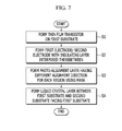
- Another exemplary embodiment of the invention provides a method of manufacturing a liquid crystal display including forming a thin film transistor connected to a gate line, on a first substrate, forming a first electrode and a second electrode, and an insulating layer between the first electrode and the second electrode, on the first substrate, forming a photo-alignment layer on the first electrode or the second electrode, disposing the first substrate facing a second substrate, and forming a liquid crystal layer between the second substrate facing the first substrate, the liquid crystal layer including a liquid crystal molecule.
- One of the first electrode and the second electrode includes a plurality of branch electrodes extending in an extension direction parallel to the gate line, and the other one of the first electrode and the second electrode has a planar shape, and the liquid crystal molecule included in the liquid crystal layer has negative dielectric anisotropy.
- the method may further include forming a data line connected to the thin film transistor and intersecting the gate line.
- the data line may extend in a straight line.
- the method may further include forming a transverse light blocking member extending in an extension direction parallel to the extension direction of the plurality of the branch electrodes, the transverse light blocking member overlapping the gate line, and forming a longitudinal light blocking member extending in an extension direction perpendicular to the extension direction of the plurality of the branch electrodes, the longitudinal light blocking member overlapping the data line.
- a width of the transverse light blocking member taken perpendicular to the extension direction thereof is larger than a width of the longitudinal light blocking member taken perpendicular to the extension direction thereof.
- the method may further include defining a plurality of pixels on the first substrate, a pixel among the plurality of pixels including an upper region and a lower region.
- the forming the photo-alignment layer may include masking the lower region of the pixel to incline a major axis of the liquid crystal molecule in the upper region at a first tilt angle, and masking the upper region of the pixel to incline a major axis of the liquid crystal molecule in the lower region at a second tilt angle, where the first tilt angle and the second tilt angle are formed different from each other.
- the method may further include defining a plurality of pixels on the first substrate, for which a first pixel is adjacent to a second pixel and a plurality of liquid crystal molecules is disposed in each of the first pixel and the second pixel.
- the forming the photo-alignment layer may include masking the second pixel to incline a major axis of the liquid crystal molecules in the first pixel at a first tilt angle, and masking the first pixel to incline a major axis of the liquid crystal molecules in the second pixel at a second tilt angle, where the first tilt angle and the second tilt angle are different from each other.
- branch electrodes of a field-generating electrodes extend in a short side direction of a pixel, and an initial alignment direction of liquid crystal molecules forms a predetermined tilt angle perpendicular to the short side direction of the pixel, thereby improving the transmittance a liquid crystal display and reducing afterimage displayed by the liquid crystal display.
- a layer when referred to as being "on" another element or substrate, the layer may be directly formed on another layer or substrate, or intervening elements may be present therebetween.
- identical reference numerals designate identical elements.
- relative terms such as “lower” or “bottom” and “upper” or “top,” may be used herein to describe one element's relationship to another element as illustrated in the Figures. It will be understood that relative terms are intended to encompass different orientations of the device in addition to the orientation depicted in the Figures. For example, if the device in one of the figures is turned over, elements described as being on the “lower” side of other elements would then be oriented on “upper” sides of the other elements. The exemplary term “lower,” can therefore, encompasses both an orientation of “lower” and “upper,” depending on the particular orientation of the figure.
- Exemplary embodiments are described herein with reference to cross section illustrations that are schematic illustrations of idealized embodiments. As such, variations from the shapes of the illustrations as a result, for example, of manufacturing techniques and/or tolerances, are to be expected. Thus, embodiments described herein should not be construed as limited to the particular shapes of regions as illustrated herein but are to include deviations in shapes that result, for example, from manufacturing. For example, a region illustrated or described as flat may, typically, have rough and/or nonlinear features. Moreover, sharp angles that are illustrated may be rounded. Thus, the regions illustrated in the figures are schematic in nature and their shapes are not intended to illustrate the precise shape of a region and are not intended to limit the scope of the present claims.
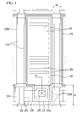
- FIG. 1 is a top plan view showing an exemplary embodiment of a liquid crystal display according to the invention.
- FIG. 2 is a cross-sectional view taken along line II-II of FIG. 1 .
- FIG. 3 is a top plan view showing an exemplary embodiment of an electrode structure in the liquid crystal display of FIG. 1 .
- a liquid crystal display includes a lower display panel 100 and an upper display panel 200 facing each other, and a liquid crystal layer 3 interposed therebetween.
- the liquid crystal display may include a display area in which an image is displayed, and a non-display area except for the display area and in which an image is not displayed.
- the display area may include a plurality of pixels.
- a pixel may include a display region in which the image is displayed and a non-display region excluding the display region in which the image is not displayed.
- a first substrate 110 includes a transparent glass, plastic or the like.
- a gate conductor including a gate line 121 is disposed on the first substrate 110.
- the gate line 121 may include a relatively wide end portion (not shown) for connection with another layer or an external driving circuit (not shown) and a gate electrode 124 protruding from a main portion thereof.
- the gate line 121 may include an aluminum (Al)-based metal such as aluminum or an aluminum alloy, a silver (Ag)-based metal such as silver or a silver alloy, a copper (Cu)-based metal such as copper or a copper alloy, a molybdenum (Mo)-based metal such as molybdenum or a molybdenum alloy, chromium (Cr), tantalum (Ta), titanium (Ti) and the like.
- the gate line 121 and portions thereof may have a single (e.g., monolayer) structure or may have a multilayer structure including at least two conductive layers having different physical properties from each other.
- a gate conductor of the liquid crystal display includes the gate line 121 and the gate electrode 124.
- the gate line 121 transmits a gate signal, and extend to extend in a horizontal direction of the plan view.
- the gate insulating layer 140 includes silicon nitride (SiNx), silicon oxide (SiOx) or the like.
- the gate insulating layer 140 may have a single (e.g., monolayer) structure or a multilayer structure including at least two insulating material layers having different physical properties from each other.
- the semiconductor layer 154 includes amorphous silicon, polysilicon or the like.
- the semiconductor layer 154 may include an oxide semiconductor.
- ohmic contacts 163 and 165 are disposed on the semiconductor layer 154.
- the ohmic contacts 163 and 165 may include a material such as n+ hydrogenated amorphous silicon doped with n-type impurities such as phosphorus at high concentration, or may include silicide.
- the ohmic contacts 163 and 165 form a pair of ohmic contacts disposed on the semiconductor layer 154.
- the ohmic contacts 163 and 165 may be omitted.
- the data line 171 includes a source electrode 173 protruded from a main portion thereof.
- a data conductor of the liquid crystal display includes the data line 171, the source electrode 173 and the drain electrode 175.
- the data line 171 includes a relatively wide end portion (not shown) for connection with another layer or an external driving circuit (not shown).
- the data line 171 transmits a data signal, and extends in a vertical direction of the plan view to intersect the gate line 121.
- the data line 171 may extend in an extension direction along the vertical direction, while intersecting the gate line 121.
- the data line 171 may not be bent and may be entirely disposed in a straight line along the vertical direction.
- the data line 171 may intersect the gate line 121 perpendicularly.
- the source electrode 173 may be a portion of the data line 171, and disposed on the same line as that of the data line 171.
- the source electrode 173 may extend in the same extension direction as that of the data line 171.
- the drain electrode 175 includes a portion extending parallel to the source electrode 173. Therefore, such an extended portion of the drain electrode 175 is parallel to a portion of the data line 171.
- the gate electrode 124, the source electrode 173 and the drain electrode 175 collectively form one thin film transistor ("TFT") together with the semiconductor layer 154.
- TFT thin film transistor
- a channel of the TFT is formed by a portion of the semiconductor layer 154 exposed between the source electrode 173 and the drain electrode 175.
- the above-described exemplary embodiment of the liquid crystal display according to the invention includes the source electrode 173 disposed on the same line as the data line 171, and the drain electrode 175 disposed to face the source electrode 173 while being parallel to the data line 171, thereby broadening a width of the TFT without widening an area occupied by the data conductor within the TFT. Accordingly, an aperture ratio of the liquid crystal display may be increased.
- the data line 171 and the drain electrode 175 includes a refractory metal such as molybdenum, chromium, tantalum, titanium, an alloy thereof or a combination of one of the foregoing.
- the data line 171 and drain electrode 175 may have a multilayer structure including a refractory metal layer (not shown) and a low resistant conductive layer (not shown). Examples of the multilayer structure include a double layer of chromium or molybdenum (alloy) lower layer and aluminum (alloy) upper layer, and a triple layer of molybdenum (alloy) lower layer, aluminum (alloy) intermediate layer and molybdenum (alloy) upper layer.
- the first passivation layer 180a may include an organic insulating material, an inorganic insulating material or the like.
- the second passivation layer 180b may include an organic insulator.
- the second passivation layer 180b may be a color filter. Where the second passivation layer 180b is a color filter, the second passivation layer 180b may uniquely display one of primary colors.
- the primary colors may include three primary colors of red, green and blue, or yellow, cyan, magenta or the like.
- the color filter may display a combination of primary colors or may be display a white color, in addition to the color filter displaying individual primary colors.
- a color filter 230 an upper display panel 200 described below may be omitted.
- the second passivation layer 180b of the lower display panel 100 includes an organic insulating material.
- a color filter (not shown) of the lower display panel 100 may be disposed between the first passivation layer 180a and the second passivation layer 180b.
- a common electrode 270 is disposed within the lower display panel 100.
- the common electrode 270 may have a planar shape in a portion corresponding to a pixel, and may have defined therein an opening 138 disposed in a region surrounding of the drain electrode 175.
- the liquid crystal display may include a plurality of common electrodes 270.
- Common electrodes 270 disposed in adjacent pixels may be connected to each other, so that common voltage having a certain level supplied from the outside of a display area of the liquid crystal display may be received by all the common electrodes 270.
- the insulating layer 180c may include an organic insulating material, an inorganic insulating material or the like.
- a pixel electrode 191 is disposed on the insulating layer 180c.
- a pixel may be defined as a region formed by the gate line 121 and the data line 171 intersecting each other, but the invention is not limited thereto.
- the pixel may have a short side and a long side longer than the short side.
- the pixel may be a minimum unit forming an image.
- the pixel electrode 191 is defined a plurality of cutouts 91 which defines a plurality of branch electrodes 192 disposed between neighboring cutouts 91. Referring to FIG.
- a plurality of the cutouts 91 is parallel to each other, and between adjacent cutouts 91, a branch electrode 192 is disposed.
- the plurality of cutouts 91 and the plurality of branch electrodes 192 may not be bent and may be entirely disposed in a straight line along the horizontal direction.
- a protrusion 191 p is extended from a main portion of the pixel electrode 191 for connection with the drain electrode 175.
- the plurality of the branch electrodes 192 extend in a short side direction of the pixel (e.g., a horizontal direction in FIG. 1 ).
- the short side direction of the pixel may be parallel to an extension direction of the gate line 121, and a long side direction of the pixel may be parallel to an extension direction of the data line 171. Consequently, the plurality of the branch electrodes 192 and the cutouts 91 may each extend parallel to the gate line 121.
- the common electrode 270 is a first field generating electrode or a first electrode of the liquid crystal display, and the pixel electrode 191 may be a second field generating electrode or a second electrode of the liquid crystal display.
- the pixel electrode 191 and the common electrode 270 may form a fringe field or the like in the liquid crystal layer 3.
- a first contact hole 185 exposing the drain electrode 175 is defined.
- the protrusion 191 p of the pixel electrode 191 is physically and electrically connected to the drain electrode 175 via the contact hole 185, thereby receiving voltage from the drain electrode 175.
- the first alignment layer 11 includes a photo-alignment layer.
- the photo-alignment layer may be undergo photolysis to form a photo-degradable alignment layer.
- the first alignment layer 11 may be formed by polymerizing at least one of cyclobutanedianhydride (“CBDA”) or a cyclobutanedianhydride (“CBDA”) derivative with a diamine.
- the cyclobutanedianhydride (“CBDA”) and the cyclobutanedianhydride (“CBDA”) derivative may include a compound represented by following Chemical Formula 1: where X1, X2, X3 and X4 are independently of one another, hydrogen, halogen, an unsubstituted or substituted alkyl group, an unsubstituted or substituted aryl group, or an unsubstituted or substituted heteroaryl group. When X1 to X4 are all hydrogen, the compound may be cyclobutanedianhydride, as represented by following Chemical Formula 1-1.
- the cyclobutandianhydride derivative includes a compound represented the following Chemical Formulas 1-2 or 1-3.
- the diamine may be a first diamine including an alkylene group as represented by -C k H 2k -, in which k is a natural number.
- the first diamine may be a compound represented by following Chemical Formula 2: where X is -(CH 2 ) h -, -S-(CH 2 ) h -S-, -O-(CH 2 ) h -O-, -(CH 2 OCH 2 ) h -, O-(CH 2 OCH 2 ) h -O-, -CH 2h1 -O-CH 2h2 -, or in which h is a natural number from 1 to 10; and h1 and h2 are natural numbers selected so that the sum of carbon atoms in the alkylene group of X is 2 to 10.
- the photo-alignment agent according to the exemplary embodiment may further include a second diamine represented by following Chemical Formula 3:
- the second diamine may be a compound of Chemical Formula 3 in which a hydrogen connected to a cyclic carbon is substituted with an alkyl group, a halogen, sulfur or the like.
- the second diamine may be an aromatic diamine such as p-phenylenediamine, m-phenylenediamine, 2,5-diaminotoluene, 2,6-diaminotoluene, 4,4'-diaminobiphenyl, 3,3'-dimethyl-4,4'-diaminobiphenyl, 3,3'-dimethoxy-4,4'-diaminobiphenyl, diaminodiphenylmethane, diaminodiphenyl ether, 2,2'-diaminodiphenyl propane, bis(3,5-diethyl-4-aminophenyl)methane, diaminodiphenylsulfone, diaminobenzophenone, diaminonaphthalene, 1,4-bis(4-aminophenoxy)benzene, 1,4-bis(4-aminophenyl)benzene, 9,10-bis(4-aminophenyl)
- a molar ratio between the first diamine and the second diamine may be 1:99 to 99:1, such as about 20:80 to 50:50.
- the upper display panel 200 will now be described.
- a second substrate 210 may include a transparent glass, plastic or the like.
- Light blocking members 220a and 220b are disposed on the second substrate 210.
- the light blocking members 220a and 220b are also referred to as a black matrix, and reduce or effectively prevent light leakage.
- the light blocking members includes a transverse light blocking member 220a covering the TFT, extending in an extension direction of a gate line 121 and overlapping the source electrode 173, the drain electrode 175, the gate electrode 124 and the like.
- the light blocking members further include a longitudinal light blocking member 220b extending in an extension direction of a data line 171 and overlapping the data line 171.
- lengths of the respective light blocking members 220a and 220b are taken in extension directions thereof, while widths are taken in directions perpendicular to the extension directions thereof.
- the width d1 of the transverse light blocking member 220a is larger than the width d2 of the longitudinal light blocking member 220b.
- an entirety of the branch electrodes 192 and the cutouts 91 extend parallel to an extension direction of a wider light blocking member among a plurality of extended light blocking members.
- the second substrate 210 On the second substrate 210 a plurality of color filters 230 is disposed.
- the color filter 230 of the upper display panel 200 may be omitted.
- the light blocking members 220a and 220b included in the upper display panel 200 may instead be disposed within the lower display panel 100.
- an overcoat 250 is disposed on the color filter 230 and the light blocking members 220a and 220b.
- the overcoat 250 may include an (organic) insulating material, and reduces or effectively prevents exposure of the color filter 230, while providing a flat surface within the upper display panel 200.
- the overcoat 250 may be omitted.
- the second alignment layer 21 may include a same material as and be formed from a same method as the first alignment layer 11 previously described.
- the liquid crystal layer 3 includes liquid crystal molecules 310 having negative dielectric anisotropy.
- the number of the liquid crystal molecule 310 shown in the drawing is one, but is a representative of a plurality of liquid crystal molecules having substantially identical properties to each other.
- the liquid crystal of the liquid crystal layer 3 may be aligned so that a major axis direction thereof is parallel to the lower and upper display panels 100 and 200.
- the pixel electrode 191 receives data voltage from the drain electrode 175, and a common electrode 270 receives common voltage having a certain level from a common voltage applying part (not shown) disposed in the outside of the display area of the liquid crystal display.
- the pixel electrode 191 and the common electrode 270 which are field generating electrodes of the liquid crystal display may generate an electric field, thereby rotating the liquid crystal molecules 310 of the liquid crystal layer 3 positioned on or overlapping the two field generating electrodes 191 and 270 in a direction perpendicular to an electric field direction.
- the polarization of light passing through the liquid crystal layer 3 is varied to control display of an image by the liquid crystal display.
- FIG. 4 is a top plan view showing a conventional liquid crystal display.
- a plurality of branch electrodes 192 extend parallel to a longitudinal light blocking member 220b.
- an initial alignment direction of liquid crystal molecules 310 in a state no electric field may be substantially perpendicular to an extension direction of the longitudinal light blocking member 220b.
- the liquid crystal display in a PLS mode refers to a liquid crystal driving mode by a plane-shaped (e.g., no cutouts defined at the liquid crystal layer) field generating electrode and a linear (e.g., with cutouts defined at the liquid crystal layer) field generating electrode overlapping each other with an insulating layer interposed therebetween.
- Ionic impurities capable of causing a line afterimage may be present in a liquid crystal layer 3 disposed between field generating electrodes.
- the liquid crystal molecule 310 of the liquid crystal layer 3 may be vibrated by heat generated therefrom during driving of the liquid crystal display.
- the ionic impurities within the liquid crystal layer 3 may move in a major axis direction of the liquid crystal molecule 310.
- a viewable afterimage may be generated thereby to reduce display quality of the liquid crystal display. As shown in FIG.
- the ionic impurities may move in a horizontal direction (indicated by the arrow) and may be accumulated at the longitudinal light blocking member 220b and an area adjacent thereto.
- a width d2 of the longitudinal light blocking member 220b is smaller than a width d1 of the transverse light blocking member 220a, the afterimage generated due to the accumulated ionic impurities at the longitudinal light blocking member 220b is more visible.
- the initial alignment of the liquid crystal molecules 310 may be perpendicular to an extension direction of the branch electrodes 192 and the transverse light blocking member 220a. Accordingly, the ionic impurities within the liquid crystal layer 3 move in a major axis direction of the liquid crystal molecule 310, such that the ionic impurities are accumulated at the transverse light blocking member 220a and an area adjacent thereto.
- the width d1 of the transverse light blocking member 220a is relatively large as compared to the width d2 of the longitudinal light blocking member 220b, the afterimage generated due to the accumulated ionic impurities at the transverse light blocking member 220a is less viewable.
- FIG. 5 is a schematic diagram showing an exemplary embodiment of an aligned state of liquid crystal molecules in a liquid crystal display according to the invention.
- a major axis of the liquid crystal molecule 310 may be aligned in a direction substantially perpendicular to a transverse light blocking member 220a.
- a pixel as a minimum unit forming an image (hereinafter referred to as a "unit pixel") includes an upper region A and a lower region B.
- a major axis of the liquid crystal molecule 310 in the upper region A is elongated in a first direction
- a major axis of the liquid crystal molecule 310 in the lower region B is elongated in a second direction.
- the first direction and the second direction may be different from each other.
- the first direction may be tilted or inclined by a predetermined tilt angle ⁇ taken in a same (rotational) direction with respect to a reference direction perpendicular to an extension direction of the transverse light blocking member 220a, the reference direction indicated by the vertical dotted line in FIG. 5 . Due to the tilt angle of the inclined liquid crystal molecule 310 for each region in the unit pixel, two domains may be formed in the unit pixel, and transmittance thereof may be improved. In an exemplary embodiment of manufacturing a liquid crystal display, the tilt angles of the first direction and the second direction being different from each other may be formed by a photo-alignment process.
- the predetermined tilt angle ⁇ may be about 1 degree (°) to about 10 degrees (°), such as about 5 ° to about 10 °.
- the common electrode 270 has a planar plane shape, and the pixel electrode 191 has a plurality of branch electrodes defined therein, but the invention is not limited thereto.
- the pixel electrode 191 has a planar plane shape, and the common electrode 270 has a plurality of branch electrodes defined therein.
- One or more exemplary embodiment according to the invention may be applied to any number of display devices in which a plane shape field generating electrode overlaps a field generating electrode having branch electrodes with an insulating layer interposed therebetween.
- FIG. 6 is a schematic drawing showing an exemplary embodiment of aligned states of liquid crystal molecules in a plurality of pixels of a liquid crystal display according to the invention.
- FIG. 6 The structure of FIG. 6 , is substantially the same as that of the exemplary embodiment described in FIGS. 1 to 3 and 5 , but the liquid crystal molecules 310 positioned in a single one unit pixel of FIG. 6 may have a substantially identical alignment to each other within that single one unit pixel.
- the number of the liquid crystal molecule 310 illustrated in a unit pixel is one, but is only representative of a plurality of the liquid crystal molecules 310 within the same unit pixel having substantially identical properties as each other.
- the liquid crystal display of FIG. 6 includes a plurality of unit pixels, and a first pixel and a second pixel vertically neighboring each other in the plan view among the plurality of the unit pixels have different liquid crystal alignments from each other.
- the liquid crystal molecules 310 positioned therein have a substantially identical alignment to each other.
- a photo-alignment layer having different alignment directions from each other may be respectively formed in areas of the first pixel and the second pixel.
- FIG. 7 is a flowchart showing an exemplary embodiment of a method of manufacturing a liquid crystal display according to the invention.
- a TFT is formed (e.g., provided) on a first substrate within a first display panel (S1).
- the TFT may collectively include a gate electrode 124, a source electrode 173, a drain electrode 175 and a semiconductor layer 154, such as described with respect to FIGS. 1 and 2 .
- One or more passivation layer is formed within the first display panel so as to cover the TFT.
- a common electrode as a first electrode, an insulating layer, and a pixel electrode as a second electrode may be formed in turn within the first display panel (S2).
- one or more photo-alignment layer having different alignment directions corresponding to unit pixels and/or regions thereof is formed such as by using a mask.
- An overall baking method may include more than one process such as a (first) prebaking process and a (second) hard baking process.
- a portion of polyamic acid contained in the photo-alignment agent material may be converted into polyimide.
- the prebaked photo-alignment agent material may be irradiated with polarized light to form a photo-degradable alignment layer.
- polarized light ultraviolet rays in a range of about 240 nanometers (nm) to about 380 nm may be used. In an exemplary embodiment, ultraviolet rays at about 254 nm may be used.
- the polarized light may have energy of about 0.20 joule per squared centimeter (J/cm 2 ) to about 1.0 J/cm 2 , such as about 0.40 J/cm 2 to about 0.50 J/cm 2 .
- the photo-alignment layer may be baked once more (hereinafter, referred to as a second baking process).
- photolyzed molecules may be rearranged to increase anisotropy.
- a second display panel is prepared, such as including elements or layers thereof formed on a second substrate.
- a liquid crystal layer including the liquid crystal molecules is formed between the first display panel including the first substrate with layers thereon and the second display panel including the second substrate with layers thereon facing the first substrate (S4).
Landscapes
- Physics & Mathematics (AREA)
- Nonlinear Science (AREA)
- General Physics & Mathematics (AREA)
- Chemical & Material Sciences (AREA)
- Crystallography & Structural Chemistry (AREA)
- Optics & Photonics (AREA)
- Mathematical Physics (AREA)
- Engineering & Computer Science (AREA)
- Microelectronics & Electronic Packaging (AREA)
- Geometry (AREA)
- Spectroscopy & Molecular Physics (AREA)
- Liquid Crystal (AREA)
- Manufacturing & Machinery (AREA)
Abstract
Description
- The invention relates to a liquid crystal display and a method of manufacturing the same.
- A liquid crystal display which is one of the most widely used flat panel displays, includes two display panels on which field generating electrodes such as a pixel electrode and a common electrode are disposed, and a liquid crystal layer interposed between the two display panels. The liquid crystal display displays images by applying voltage to the field generating electrodes to produce an electric field in the liquid crystal layer, through which alignment of liquid crystal molecules of the liquid crystal layer is determined, and controlling polarization of incident light thereto.
- In order to increase display quality of a liquid crystal display, implementing a liquid crystal display having a relatively high contrast ratio, excellent wide viewing angle and quick response speed is desired. In addition to increasing the display quality of the liquid crystal display, preventing display quality deterioration thereof is also desired. Such display deterioration may be a result of stains generated due to disarrangement of liquid crystal molecule caused by an external influence to the liquid crystal display such as pressure and the like.
- For a liquid crystal layer of a liquid crystal display, liquid crystals in the liquid crystal layer include a positive dielectric anisotropy liquid crystal and a negative dielectric anisotropy liquid crystal. The negative dielectric anisotropy liquid crystal has a relatively high rotational elastic energy due to a small splay angle of surrounding liquid crystals, as compared with the positive dielectric anisotropy liquid crystal. Thus, the negative dielectric anisotropy liquid crystal has relatively high transmittance.
- However, since the negative dielectric anisotropy liquid crystal includes more ionic impurities than the positive dielectric anisotropy liquid crystal, severe afterimage may be generated by using the negative dielectric anisotropy liquid crystal.
- One or more exemplary embodiment of the invention provides a liquid crystal display and a method of manufacturing the same to improve a display quality of the liquid crystal display by reducing afterimage.
- An exemplary embodiment of the invention provides a liquid crystal display including a first substrate, a gate line on the first substrate, a thin film transistor disposed on the first substrate and connected to the gate line, a first electrode and a second electrode on the first substrate, an insulating layer between the first electrode and the second electrode, a second substrate facing the first substrate, and a liquid crystal layer between the first substrate and the second substrate and including a liquid crystal molecule. One of the first electrode and the second electrode includes a plurality of branch electrodes, and the other one of the first electrode and the second electrode has a planar shape. The plurality of the branch electrodes extend in an extension direction parallel to the gate line. The liquid crystal molecule of the liquid crystal layer has negative dielectric anisotropy.
- A major axis of the liquid crystal molecule may form a tilt angle with a direction perpendicular to the extension direction of the plurality of the branch electrodes in a state of no electric field applied to the liquid crystal layer.
- The plurality of the branch electrodes of the one of the first electrode and the second electrode may overlap the planar shape of the other one of the first electrode and the second electrode.
- The one of the first electrode and the second electrode including the plurality of branch electrodes may be connected to the thin film transistor.
- The liquid crystal display may further include a photo-alignment layer on the plurality of the branch electrodes of the one of the first electrode and the second electrode. The photo-alignment layer may determine the tilt angle of the liquid crystal molecule.
- The liquid crystal display may further include a data line connected to the thin film transistor and intersecting the gate line. The data line may extend in a straight line.
- The liquid crystal display may further include a transverse light blocking member extending in an extension direction parallel to the extension direction of the plurality of the branch electrodes, the transverse light blocking member overlapping the gate line, and a longitudinal light blocking member extending in an extension direction perpendicular to the extension direction of the plurality of the branch electrodes, the longitudinal light blocking member overlapping the data line may be further included. A width of the transverse light blocking member taken perpendicular to the extension direction thereof may be larger than a width of the longitudinal light blocking member taken perpendicular to the extension direction thereof.
- The gate line and the data line may perpendicularly intersect each other.
- A plurality of pixels may be defined on the first substrate, each pixel among the plurality of the pixels including a short sides in the extension direction of the plurality of branch electrodes and a long side in a direction perpendicular to the extension direction of the plurality of the branch electrodes.
- The photo-alignment layer may be a photo-degradable alignment layer.
- A plurality of pixels may be defined on the first substrate, each pixel among the plurality of the pixels may include an upper region and a lower region. A major axis of the liquid crystal molecule disposed in the upper region forms a first tilt angle with the direction perpendicular to the extension direction of the plurality of the branch electrodes in the state of no electric field applied to the liquid crystal layer, and a major axis of the liquid crystal molecule disposed in the lower region forms a second tilt angle with the direction perpendicular to the extension direction of the plurality of the branch electrodes in the state of no electric field applied to the liquid crystal layer. The first tilt angle and the second tilt angle may be different from each other.
- A plurality of pixels may be defined on the first substrate, among which a first pixel is adjacent to a second pixel and a plurality of liquid crystal molecules is disposed in each of the first pixel and the second pixel. A major axis of each of the liquid crystal molecules disposed in the first pixel forms a first tilt angle with the direction perpendicular to the extension direction of the plurality of the branch electrodes in the state of no electric field applied to the liquid crystal layer, and a major axis of each of the liquid crystal molecules disposed in the second pixel forms a second tilt angle with the direction perpendicular to the extension direction of the plurality of the branch electrodes in the state of no electric field applied to the liquid crystal layer. The first tilt angle and the second tilt angle may be different from each other.
- The tilt angle may be about 5 degrees to about 10 degrees.
- When the liquid crystal layer includes ionic impurities, the ionic impurities in the liquid crystal layer may be accumulated at the gate line.
- The transverse light blocking member extending in the extension direction parallel to the extension direction of the plurality of the branch electrodes may overlap the ionic impurities accumulated at the gate line.
- Another exemplary embodiment of the invention provides a method of manufacturing a liquid crystal display including forming a thin film transistor connected to a gate line, on a first substrate, forming a first electrode and a second electrode, and an insulating layer between the first electrode and the second electrode, on the first substrate, forming a photo-alignment layer on the first electrode or the second electrode, disposing the first substrate facing a second substrate, and forming a liquid crystal layer between the second substrate facing the first substrate, the liquid crystal layer including a liquid crystal molecule. One of the first electrode and the second electrode includes a plurality of branch electrodes extending in an extension direction parallel to the gate line, and the other one of the first electrode and the second electrode has a planar shape, and the liquid crystal molecule included in the liquid crystal layer has negative dielectric anisotropy.
- The method may further include forming a data line connected to the thin film transistor and intersecting the gate line. The data line may extend in a straight line.
- The method may further include forming a transverse light blocking member extending in an extension direction parallel to the extension direction of the plurality of the branch electrodes, the transverse light blocking member overlapping the gate line, and forming a longitudinal light blocking member extending in an extension direction perpendicular to the extension direction of the plurality of the branch electrodes, the longitudinal light blocking member overlapping the data line. A width of the transverse light blocking member taken perpendicular to the extension direction thereof is larger than a width of the longitudinal light blocking member taken perpendicular to the extension direction thereof.
- The method may further include defining a plurality of pixels on the first substrate, a pixel among the plurality of pixels including an upper region and a lower region. The forming the photo-alignment layer may include masking the lower region of the pixel to incline a major axis of the liquid crystal molecule in the upper region at a first tilt angle, and masking the upper region of the pixel to incline a major axis of the liquid crystal molecule in the lower region at a second tilt angle, where the first tilt angle and the second tilt angle are formed different from each other.
- The method may further include defining a plurality of pixels on the first substrate, for which a first pixel is adjacent to a second pixel and a plurality of liquid crystal molecules is disposed in each of the first pixel and the second pixel. The forming the photo-alignment layer may include masking the second pixel to incline a major axis of the liquid crystal molecules in the first pixel at a first tilt angle, and masking the first pixel to incline a major axis of the liquid crystal molecules in the second pixel at a second tilt angle, where the first tilt angle and the second tilt angle are different from each other.
- According to one or more exemplary embodiment of the invention, branch electrodes of a field-generating electrodes extend in a short side direction of a pixel, and an initial alignment direction of liquid crystal molecules forms a predetermined tilt angle perpendicular to the short side direction of the pixel, thereby improving the transmittance a liquid crystal display and reducing afterimage displayed by the liquid crystal display.
- The above and other advantages and features of this disclosure will become more apparent by describing in further detail exemplary embodiments thereof with reference to the accompanying drawings, in which:
-
FIG. 1 is a top plan view showing an exemplary embodiment of a liquid crystal display according to the invention. -
FIG. 2 is a cross-sectional view taken along line II-II ofFIG. 1 . -
FIG. 3 is a top plan view showing an exemplary embodiment of an electrode structure in the liquid crystal display ofFIG. 1 . -
FIG. 4 is a top plan view showing a conventional liquid crystal display. -
FIG. 5 is a schematic diagram showing an exemplary embodiment of an aligned state of a liquid crystal molecule in a liquid crystal display according to the invention. -
FIG. 6 is a schematic diagram showing an exemplary embodiment of aligned states of liquid crystal molecules in a plurality of pixels in a liquid crystal display according to the invention. -
FIG. 7 is a flowchart showing an exemplary embodiment of a method of manufacturing a liquid crystal display according to the invention. - Referring to accompanying drawings, exemplary embodiments of the invention will be described in detail. However, the invention is not limited to the exemplary embodiments described herein, and may be embodied in other forms. Rather, the exemplary embodiments introduced herein are provided so that the disclosure may become thorough and complete, and the spirit of the invention may be sufficiently delivered to those skilled in the art.
- It will be understood that, although the terms "first," "second," "third" etc. may be used herein to describe various elements, components, regions, layers and/or sections, these elements, components, regions, layers and/or sections should not be limited by these terms. These terms are only used to distinguish one element, component, region, layer or section from another element, component, region, layer or section. Thus, "a first element," "component," "region," "layer" or "section" discussed below could be termed a second element, component, region, layer or section without departing from the teachings herein. In the drawings, the thicknesses of layers and regions are exaggerated for clarity
- Further, when a layer is referred to as being "on" another element or substrate, the layer may be directly formed on another layer or substrate, or intervening elements may be present therebetween. Throughout the specification, identical reference numerals designate identical elements.
- The terminology used herein is for the purpose of describing particular embodiments only and is not intended to be limiting. As used herein, the singular forms "a," "an," and "the" are intended to include the plural forms, including "at least one," unless the content clearly indicates otherwise. "Or" means "and/or." As used herein, the term "and/or" includes any and all combinations of one or more of the associated listed items. It will be further understood that the terms "comprises" and/or "comprising," or "includes" and/or "including" when used in this specification, specify the presence of stated features, regions, integers, steps, operations, elements, and/or components, but do not preclude the presence or addition of one or more other features, regions, integers, steps, operations, elements, components, and/or groups thereof.
- Furthermore, relative terms, such as "lower" or "bottom" and "upper" or "top," may be used herein to describe one element's relationship to another element as illustrated in the Figures. It will be understood that relative terms are intended to encompass different orientations of the device in addition to the orientation depicted in the Figures. For example, if the device in one of the figures is turned over, elements described as being on the "lower" side of other elements would then be oriented on "upper" sides of the other elements. The exemplary term "lower," can therefore, encompasses both an orientation of "lower" and "upper," depending on the particular orientation of the figure. Similarly, if the device in one of the figures is turned over, elements described as "below" or "beneath" other elements would then be oriented "above" the other elements. The exemplary terms "below" or "beneath" can, therefore, encompass both an orientation of above and below.
- "About" or "approximately" as used herein is inclusive of the stated value and means within an acceptable range of deviation for the particular value as determined by one of ordinary skill in the art, considering the measurement in question and the error associated with measurement of the particular quantity (i.e., the limitations of the measurement system). For example, "about" can mean within one or more standard deviations, or within ± 30%, 20%, 10%, 5% of the stated value.
- Unless otherwise defined, all terms (including technical and scientific terms) used herein have the same meaning as commonly understood by one of ordinary skill in the art to which this disclosure belongs. It will be further understood that terms, such as those defined in commonly used dictionaries, should be interpreted as having a meaning that is consistent with their meaning in the context of the relevant art and the present disclosure, and will not be interpreted in an idealized or overly formal sense unless expressly so defined herein.
- Exemplary embodiments are described herein with reference to cross section illustrations that are schematic illustrations of idealized embodiments. As such, variations from the shapes of the illustrations as a result, for example, of manufacturing techniques and/or tolerances, are to be expected. Thus, embodiments described herein should not be construed as limited to the particular shapes of regions as illustrated herein but are to include deviations in shapes that result, for example, from manufacturing. For example, a region illustrated or described as flat may, typically, have rough and/or nonlinear features. Moreover, sharp angles that are illustrated may be rounded. Thus, the regions illustrated in the figures are schematic in nature and their shapes are not intended to illustrate the precise shape of a region and are not intended to limit the scope of the present claims.
-
FIG. 1 is a top plan view showing an exemplary embodiment of a liquid crystal display according to the invention.FIG. 2 is a cross-sectional view taken along line II-II ofFIG. 1 .FIG. 3 is a top plan view showing an exemplary embodiment of an electrode structure in the liquid crystal display ofFIG. 1 . - Referring to
FIGS. 1 and2 , a liquid crystal display includes alower display panel 100 and anupper display panel 200 facing each other, and a liquid crystal layer 3 interposed therebetween. The liquid crystal display may include a display area in which an image is displayed, and a non-display area except for the display area and in which an image is not displayed. The display area may include a plurality of pixels. A pixel may include a display region in which the image is displayed and a non-display region excluding the display region in which the image is not displayed. - First, the
lower display panel 100 will be described. - A
first substrate 110 includes a transparent glass, plastic or the like. A gate conductor including agate line 121 is disposed on thefirst substrate 110. - The
gate line 121 may include a relatively wide end portion (not shown) for connection with another layer or an external driving circuit (not shown) and agate electrode 124 protruding from a main portion thereof. Thegate line 121 may include an aluminum (Al)-based metal such as aluminum or an aluminum alloy, a silver (Ag)-based metal such as silver or a silver alloy, a copper (Cu)-based metal such as copper or a copper alloy, a molybdenum (Mo)-based metal such as molybdenum or a molybdenum alloy, chromium (Cr), tantalum (Ta), titanium (Ti) and the like. Thegate line 121 and portions thereof may have a single (e.g., monolayer) structure or may have a multilayer structure including at least two conductive layers having different physical properties from each other. A gate conductor of the liquid crystal display includes thegate line 121 and thegate electrode 124. Thegate line 121 transmits a gate signal, and extend to extend in a horizontal direction of the plan view. - On the
gate line 121, a gate insulating layer 140 is disposed. The gate insulating layer 140 includes silicon nitride (SiNx), silicon oxide (SiOx) or the like. The gate insulating layer 140 may have a single (e.g., monolayer) structure or a multilayer structure including at least two insulating material layers having different physical properties from each other. - On the gate insulating layer 140, a
semiconductor layer 154 is disposed. Thesemiconductor layer 154 includes amorphous silicon, polysilicon or the like. Thesemiconductor layer 154 may include an oxide semiconductor. - On the
semiconductor layer 154,ohmic contacts ohmic contacts ohmic contacts semiconductor layer 154. In an exemplary embodiment, where thesemiconductor layer 154 is an oxide semiconductor, theohmic contacts - On the
ohmic contacts data line 171 and adrain electrode 175 are disposed. Thedata line 171 includes asource electrode 173 protruded from a main portion thereof. A data conductor of the liquid crystal display includes thedata line 171, thesource electrode 173 and thedrain electrode 175. - The
data line 171 includes a relatively wide end portion (not shown) for connection with another layer or an external driving circuit (not shown). Thedata line 171 transmits a data signal, and extends in a vertical direction of the plan view to intersect thegate line 121. - Herein, the
data line 171 may extend in an extension direction along the vertical direction, while intersecting thegate line 121. Thedata line 171 may not be bent and may be entirely disposed in a straight line along the vertical direction. In an exemplary embodiment, thedata line 171 may intersect thegate line 121 perpendicularly. - The
source electrode 173 may be a portion of thedata line 171, and disposed on the same line as that of thedata line 171. Thesource electrode 173 may extend in the same extension direction as that of thedata line 171. Thedrain electrode 175 includes a portion extending parallel to thesource electrode 173. Therefore, such an extended portion of thedrain electrode 175 is parallel to a portion of thedata line 171. - The
gate electrode 124, thesource electrode 173 and thedrain electrode 175 collectively form one thin film transistor ("TFT") together with thesemiconductor layer 154. A channel of the TFT is formed by a portion of thesemiconductor layer 154 exposed between thesource electrode 173 and thedrain electrode 175. - The above-described exemplary embodiment of the liquid crystal display according to the invention includes the
source electrode 173 disposed on the same line as thedata line 171, and thedrain electrode 175 disposed to face thesource electrode 173 while being parallel to thedata line 171, thereby broadening a width of the TFT without widening an area occupied by the data conductor within the TFT. Accordingly, an aperture ratio of the liquid crystal display may be increased. - The
data line 171 and the drain electrode 175 (e.g., the data conductor) includes a refractory metal such as molybdenum, chromium, tantalum, titanium, an alloy thereof or a combination of one of the foregoing. Thedata line 171 anddrain electrode 175 may have a multilayer structure including a refractory metal layer (not shown) and a low resistant conductive layer (not shown). Examples of the multilayer structure include a double layer of chromium or molybdenum (alloy) lower layer and aluminum (alloy) upper layer, and a triple layer of molybdenum (alloy) lower layer, aluminum (alloy) intermediate layer and molybdenum (alloy) upper layer. - On exposed portions of the
data conductor semiconductor layer 154, afirst passivation layer 180a is disposed. Thefirst passivation layer 180a may include an organic insulating material, an inorganic insulating material or the like. - On the
first passivation layer 180a, asecond passivation layer 180b is disposed. Thesecond passivation layer 180b may include an organic insulator. - In an exemplary embodiment, the
second passivation layer 180b may be a color filter. Where thesecond passivation layer 180b is a color filter, thesecond passivation layer 180b may uniquely display one of primary colors. The primary colors may include three primary colors of red, green and blue, or yellow, cyan, magenta or the like. In an exemplary embodiment the color filter may display a combination of primary colors or may be display a white color, in addition to the color filter displaying individual primary colors. Where thesecond passivation layer 180b of thelower display panel 100 is the color filter, acolor filter 230 anupper display panel 200 described below may be omitted. - In another exemplary embodiment, the
second passivation layer 180b of thelower display panel 100 includes an organic insulating material. Where thesecond passivation layer 180b includes the organic insulating material, a color filter (not shown) of thelower display panel 100 may be disposed between thefirst passivation layer 180a and thesecond passivation layer 180b. - On the
second passivation layer 180b, acommon electrode 270 is disposed within thelower display panel 100. Thecommon electrode 270 may have a planar shape in a portion corresponding to a pixel, and may have defined therein anopening 138 disposed in a region surrounding of thedrain electrode 175. - The liquid crystal display may include a plurality of
common electrodes 270.Common electrodes 270 disposed in adjacent pixels may be connected to each other, so that common voltage having a certain level supplied from the outside of a display area of the liquid crystal display may be received by all thecommon electrodes 270. - On the
common electrode 270, an insulatinglayer 180c is disposed. The insulatinglayer 180c may include an organic insulating material, an inorganic insulating material or the like. - On the insulating
layer 180c, apixel electrode 191 is disposed. In an exemplary embodiment of the liquid crystal display according to the invention, a pixel may be defined as a region formed by thegate line 121 and thedata line 171 intersecting each other, but the invention is not limited thereto. The pixel may have a short side and a long side longer than the short side. The pixel may be a minimum unit forming an image. In thepixel electrode 191 is defined a plurality ofcutouts 91 which defines a plurality ofbranch electrodes 192 disposed between neighboringcutouts 91. Referring toFIG. 3 , a plurality of thecutouts 91 is parallel to each other, and betweenadjacent cutouts 91, abranch electrode 192 is disposed. The plurality ofcutouts 91 and the plurality ofbranch electrodes 192 may not be bent and may be entirely disposed in a straight line along the horizontal direction. - In the plan view, below the
pixel electrode 191, aprotrusion 191 p is extended from a main portion of thepixel electrode 191 for connection with thedrain electrode 175. - The plurality of the
branch electrodes 192 extend in a short side direction of the pixel (e.g., a horizontal direction inFIG. 1 ). The short side direction of the pixel may be parallel to an extension direction of thegate line 121, and a long side direction of the pixel may be parallel to an extension direction of thedata line 171. Consequently, the plurality of thebranch electrodes 192 and thecutouts 91 may each extend parallel to thegate line 121. - The
common electrode 270 is a first field generating electrode or a first electrode of the liquid crystal display, and thepixel electrode 191 may be a second field generating electrode or a second electrode of the liquid crystal display. Thepixel electrode 191 and thecommon electrode 270 may form a fringe field or the like in the liquid crystal layer 3. - In the
first passivation layer 180a, thesecond passivation layer 180b and the insulatinglayer 180c, afirst contact hole 185 exposing thedrain electrode 175 is defined. Theprotrusion 191 p of thepixel electrode 191 is physically and electrically connected to thedrain electrode 175 via thecontact hole 185, thereby receiving voltage from thedrain electrode 175. - On the
pixel electrode 191 and the insulatinglayer 180c, afirst alignment layer 11 is disposed. Thefirst alignment layer 11 includes a photo-alignment layer. - In an exemplary embodiment, the photo-alignment layer may be undergo photolysis to form a photo-degradable alignment layer. In an exemplary embodiment of manufacturing a liquid crystal display, for example, the
first alignment layer 11 may be formed by polymerizing at least one of cyclobutanedianhydride ("CBDA") or a cyclobutanedianhydride ("CBDA") derivative with a diamine. - The cyclobutanedianhydride ("CBDA") and the cyclobutanedianhydride ("CBDA") derivative may include a compound represented by following Chemical Formula 1:
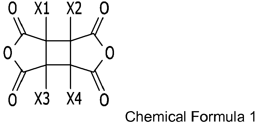

- The cyclobutandianhydride derivative includes a compound represented the following Chemical Formulas 1-2 or 1-3.


- In the exemplary embodiment, the diamine may be a first diamine including an alkylene group as represented by -CkH2k-, in which k is a natural number. The first diamine may be a compound represented by following Chemical Formula 2:


- The photo-alignment agent according to the exemplary embodiment may further include a second diamine represented by following Chemical Formula 3:
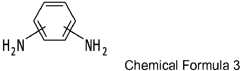
- The second diamine may be a compound of Chemical Formula 3 in which a hydrogen connected to a cyclic carbon is substituted with an alkyl group, a halogen, sulfur or the like.
- The second diamine may be an aromatic diamine such as p-phenylenediamine, m-phenylenediamine, 2,5-diaminotoluene, 2,6-diaminotoluene, 4,4'-diaminobiphenyl, 3,3'-dimethyl-4,4'-diaminobiphenyl, 3,3'-dimethoxy-4,4'-diaminobiphenyl, diaminodiphenylmethane, diaminodiphenyl ether, 2,2'-diaminodiphenyl propane, bis(3,5-diethyl-4-aminophenyl)methane, diaminodiphenylsulfone, diaminobenzophenone, diaminonaphthalene, 1,4-bis(4-aminophenoxy)benzene, 1,4-bis(4-aminophenyl)benzene, 9,10-bis(4-aminophenyl)anthracene, 1,3-bis(4-aminophenoxy)benzene, 4,4'-bis(4-aminophenoxy)diphenylsulfone, 2,2-bis[4-(4-aminophenoxy)phenyl]propane, 2,2-bis(4-aminophenyl)hexafluoropropane and 2,2-bis[4-(4-aminophenoxy)phenyl]hexafluoropropane; an alicyclic diamine such as bis(4-aminocyclohexyl)methane and bis(4-amino-3-methylcyclohexyl)methane; or an aliphatic diamine such as tetramethylenediamine and hexamethylenediamine, and the like. However, the second diamine is not particularly limited thereto, and most diamines having an inflexible property, with the exception of first diamine compounds, may be used.
- In an exemplary embodiment, a molar ratio between the first diamine and the second diamine may be 1:99 to 99:1, such as about 20:80 to 50:50.
- The
upper display panel 200 will now be described. - A
second substrate 210 may include a transparent glass, plastic or the like.Light blocking members second substrate 210. Thelight blocking members light blocking member 220a covering the TFT, extending in an extension direction of agate line 121 and overlapping thesource electrode 173, thedrain electrode 175, thegate electrode 124 and the like. The light blocking members further include a longitudinallight blocking member 220b extending in an extension direction of adata line 171 and overlapping thedata line 171. - Referring to
FIG. 1 , lengths of the respectivelight blocking members FIG. 1 , the width d1 of the transverselight blocking member 220a is larger than the width d2 of the longitudinallight blocking member 220b. In the exemplary embodiment, an entirety of thebranch electrodes 192 and thecutouts 91 extend parallel to an extension direction of a wider light blocking member among a plurality of extended light blocking members. - On the second substrate 210 a plurality of
color filters 230 is disposed. Where thesecond passivation layer 180b within thelower display panel 100 is a color filter, or a color filter which is not thesecond passivation layer 180b is disposed within thelower display panel 100, thecolor filter 230 of theupper display panel 200 may be omitted. Different from the illustrated exemplary embodiment, thelight blocking members upper display panel 200 may instead be disposed within thelower display panel 100. - On the
color filter 230 and thelight blocking members overcoat 250 is disposed. Theovercoat 250 may include an (organic) insulating material, and reduces or effectively prevents exposure of thecolor filter 230, while providing a flat surface within theupper display panel 200. In an exemplary embodiment, theovercoat 250 may be omitted. - On the
overcoat 250, asecond alignment layer 21 is disposed. Thesecond alignment layer 21 may include a same material as and be formed from a same method as thefirst alignment layer 11 previously described. - In the exemplary embodiment, the liquid crystal layer 3 includes
liquid crystal molecules 310 having negative dielectric anisotropy. The number of theliquid crystal molecule 310 shown in the drawing is one, but is a representative of a plurality of liquid crystal molecules having substantially identical properties to each other. - The liquid crystal of the liquid crystal layer 3 may be aligned so that a major axis direction thereof is parallel to the lower and
upper display panels - The
pixel electrode 191 receives data voltage from thedrain electrode 175, and acommon electrode 270 receives common voltage having a certain level from a common voltage applying part (not shown) disposed in the outside of the display area of the liquid crystal display. - The
pixel electrode 191 and thecommon electrode 270 which are field generating electrodes of the liquid crystal display may generate an electric field, thereby rotating theliquid crystal molecules 310 of the liquid crystal layer 3 positioned on or overlapping the twofield generating electrodes liquid crystal molecules 310 as determined by the electric field applied thereto, the polarization of light passing through the liquid crystal layer 3 is varied to control display of an image by the liquid crystal display. - As such, by forming two
field generating electrodes lower display panel 100, transmittance of the liquid crystal display may be increased, and a relatively wide viewing angle may be implemented. -
FIG. 4 is a top plan view showing a conventional liquid crystal display. - Referring to
FIG. 4 , in a conventional liquid crystal display in a plane-to-line switching ("PLS") mode, a plurality ofbranch electrodes 192 extend parallel to a longitudinallight blocking member 220b. As indicated by the horizontal arrow inFIG. 4 , an initial alignment direction ofliquid crystal molecules 310 in a state no electric field may be substantially perpendicular to an extension direction of the longitudinallight blocking member 220b. The liquid crystal display in a PLS mode refers to a liquid crystal driving mode by a plane-shaped (e.g., no cutouts defined at the liquid crystal layer) field generating electrode and a linear (e.g., with cutouts defined at the liquid crystal layer) field generating electrode overlapping each other with an insulating layer interposed therebetween. - Ionic impurities capable of causing a line afterimage may be present in a liquid crystal layer 3 disposed between field generating electrodes. The
liquid crystal molecule 310 of the liquid crystal layer 3 may be vibrated by heat generated therefrom during driving of the liquid crystal display. As a result, the ionic impurities within the liquid crystal layer 3 may move in a major axis direction of theliquid crystal molecule 310. When the moved ionic impurities are accumulated, a viewable afterimage may be generated thereby to reduce display quality of the liquid crystal display. As shown inFIG. 4 , whereliquid crystal molecules 310 are initially aligned perpendicular to thebranch electrode 192, the ionic impurities may move in a horizontal direction (indicated by the arrow) and may be accumulated at the longitudinallight blocking member 220b and an area adjacent thereto. Herein, since a width d2 of the longitudinallight blocking member 220b is smaller than a width d1 of the transverselight blocking member 220a, the afterimage generated due to the accumulated ionic impurities at the longitudinallight blocking member 220b is more visible. - In one or more exemplary embodiment according to the invention, since a plurality of
branch electrodes 192 are elongated in an extension direction of a short side of the pixel, such extension direction being parallel to thegate line 121 and parallel to the widerlight blocking member 220a, the initial alignment of theliquid crystal molecules 310 may be perpendicular to an extension direction of thebranch electrodes 192 and the transverselight blocking member 220a. Accordingly, the ionic impurities within the liquid crystal layer 3 move in a major axis direction of theliquid crystal molecule 310, such that the ionic impurities are accumulated at the transverselight blocking member 220a and an area adjacent thereto. Since the width d1 of the transverselight blocking member 220a is relatively large as compared to the width d2 of the longitudinallight blocking member 220b, the afterimage generated due to the accumulated ionic impurities at the transverselight blocking member 220a is less viewable. -
FIG. 5 is a schematic diagram showing an exemplary embodiment of an aligned state of liquid crystal molecules in a liquid crystal display according to the invention. - Referring to
FIG. 5 , a major axis of theliquid crystal molecule 310 may be aligned in a direction substantially perpendicular to a transverselight blocking member 220a. In the exemplary embodiment, a pixel as a minimum unit forming an image (hereinafter referred to as a "unit pixel") includes an upper region A and a lower region B. A major axis of theliquid crystal molecule 310 in the upper region A is elongated in a first direction, and a major axis of theliquid crystal molecule 310 in the lower region B is elongated in a second direction. Herein, the first direction and the second direction may be different from each other. In an exemplary embodiment, for example, the first direction may be tilted or inclined by a predetermined tilt angle Θ taken in a same (rotational) direction with respect to a reference direction perpendicular to an extension direction of the transverselight blocking member 220a, the reference direction indicated by the vertical dotted line inFIG. 5 . Due to the tilt angle of the inclinedliquid crystal molecule 310 for each region in the unit pixel, two domains may be formed in the unit pixel, and transmittance thereof may be improved. In an exemplary embodiment of manufacturing a liquid crystal display, the tilt angles of the first direction and the second direction being different from each other may be formed by a photo-alignment process. In an exemplary embodiment, the predetermined tilt angle Θ may be about 1 degree (°) to about 10 degrees (°), such as about 5 ° to about 10 °. - In the previously described exemplary embodiments of the liquid crystal display according to the invention, the
common electrode 270 has a planar plane shape, and thepixel electrode 191 has a plurality of branch electrodes defined therein, but the invention is not limited thereto. In an alternative exemplary embodiment according to the invention, thepixel electrode 191 has a planar plane shape, and thecommon electrode 270 has a plurality of branch electrodes defined therein. - One or more exemplary embodiment according to the invention may be applied to any number of display devices in which a plane shape field generating electrode overlaps a field generating electrode having branch electrodes with an insulating layer interposed therebetween.
-
FIG. 6 is a schematic drawing showing an exemplary embodiment of aligned states of liquid crystal molecules in a plurality of pixels of a liquid crystal display according to the invention. - The structure of
FIG. 6 , is substantially the same as that of the exemplary embodiment described inFIGS. 1 to 3 and5 , but theliquid crystal molecules 310 positioned in a single one unit pixel ofFIG. 6 may have a substantially identical alignment to each other within that single one unit pixel. The number of theliquid crystal molecule 310 illustrated in a unit pixel is one, but is only representative of a plurality of theliquid crystal molecules 310 within the same unit pixel having substantially identical properties as each other. - The liquid crystal display of
FIG. 6 includes a plurality of unit pixels, and a first pixel and a second pixel vertically neighboring each other in the plan view among the plurality of the unit pixels have different liquid crystal alignments from each other. Within each unit pixel, theliquid crystal molecules 310 positioned therein have a substantially identical alignment to each other. In an exemplary embodiment of manufacturing a liquid crystal display, in order to form the above-described liquid crystal alignment, a photo-alignment layer having different alignment directions from each other may be respectively formed in areas of the first pixel and the second pixel. - Hereinafter, referring to
FIG. 7 , a method of manufacturing a liquid crystal display according to the invention, will be described. The invention is not limited to the exemplary embodiment described below but may be varied in other forms. -
FIG. 7 is a flowchart showing an exemplary embodiment of a method of manufacturing a liquid crystal display according to the invention. - Referring to
FIG. 7 , a TFT is formed (e.g., provided) on a first substrate within a first display panel (S1). The TFT may collectively include agate electrode 124, asource electrode 173, adrain electrode 175 and asemiconductor layer 154, such as described with respect toFIGS. 1 and2 . - One or more passivation layer is formed within the first display panel so as to cover the TFT. On the one or more passivation layer, a common electrode as a first electrode, an insulating layer, and a pixel electrode as a second electrode may be formed in turn within the first display panel (S2).
- Thereafter, on the pixel electrode, one or more photo-alignment layer having different alignment directions corresponding to unit pixels and/or regions thereof is formed such as by using a mask.
- A method of forming the photo-alignment layer will be described below. On the pixel electrode, a photo-alignment agent material is applied, and the applied photo-alignment agent material is baked. An overall baking method may include more than one process such as a (first) prebaking process and a (second) hard baking process.
- In the prebaking process, a portion of polyamic acid contained in the photo-alignment agent material may be converted into polyimide. Thereafter, the prebaked photo-alignment agent material may be irradiated with polarized light to form a photo-degradable alignment layer. As the irradiated light, ultraviolet rays in a range of about 240 nanometers (nm) to about 380 nm may be used. In an exemplary embodiment, ultraviolet rays at about 254 nm may be used. The polarized light may have energy of about 0.20 joule per squared centimeter (J/cm2) to about 1.0 J/cm2, such as about 0.40 J/cm2 to about 0.50 J/cm2.
- Referring to S3 in
FIG. 7 and the exemplary embodiment inFIG. 5 , in a state where the lower region B of the unit pixel is masked, the upper region A of the unit pixel is irradiated with polarized light, thereby forming an alignment direction in the first direction. Thereafter, in a state where the upper region A of the unit pixel is masked, the lower region B of the unit pixel is irradiated with polarized light, thereby forming an alignment direction in the second direction. - Referring to S3 in
FIG. 7 and the exemplary embodiment inFIG. 6 , to make different alignment directions between vertically neighboring unit pixels, in a state where one of the neighboring unit pixels is irradiated with polarized light to form the alignment direction thereof, one or more other unit pixels to have a different alignment direction from that of the one neighboring unit pixel is masked. - In order to increase an alignment within the unit pixels, the photo-alignment layer may be baked once more (hereinafter, referred to as a second baking process). Herein, photolyzed molecules may be rearranged to increase anisotropy.
- A second display panel is prepared, such as including elements or layers thereof formed on a second substrate.
- Thereafter, a liquid crystal layer including the liquid crystal molecules is formed between the first display panel including the first substrate with layers thereon and the second display panel including the second substrate with layers thereon facing the first substrate (S4).
- As above, exemplary embodiments of the invention have been described in detail, but the invention is not limited thereto. Variations and modifications by a person skilled in the art using a basic concept of the invention as defined in the claims below, also belong to the scope of the invention.
- While this invention has been described in connection with what is presently considered to be practical exemplary embodiments, the invention is not limited to the disclosed exemplary embodiments, but, on the contrary, is intended to cover various modifications and equivalent arrangements included within the scope of the appended claims.
Claims (20)
- A liquid crystal display, comprising:a first substrate (110),a gate line (121) on the first substrate (110),a thin film transistor (TFT) disposed on the first substrate (110), connected to the gate line (121),a first electrode and a second electrode on the first substrate (110),an insulating layer (180c) between the first electrode and the second electrode,a second substrate (210) facing the first substrate (110), anda liquid crystal layer (3) between the first substrate (110) and the second substrate (210), the liquid crystal layer (3) comprising a liquid crystal molecule (310),whereinone of the first electrode and the second electrode includes a plurality of branch electrodes (192), and the other one of the first electrode and the second electrode has a planar shape,the plurality of the branch electrodes (192) extend in an extension direction parallel to the gate line (121), andthe liquid crystal molecule (310) of the liquid crystal layer (3) has negative dielectric anisotropy.
- The liquid crystal display of claim 1, wherein:a major axis of the liquid crystal molecule (310) forms a tilt angle (Θ) with a direction perpendicular to the extension direction of the plurality of the branch electrodes (192) in a state of no electric field applied to the liquid crystal layer (3).
- The liquid crystal display of one of claims 1 or 2, wherein:the plurality of the branch electrodes (192) of the one of the first electrode and the second electrode overlaps the planar shape of the other one of the first electrode and the second electrode.
- The liquid crystal display of one of claims 1 to 3, wherein:the one of the first electrode and the second electrode including the plurality of branch electrodes (192) is connected to the thin film transistor (TFT).
- The liquid crystal display of one of claims 2 to 4, further comprising:a photo-alignment layer on the plurality of the branch electrodes (192) of the one of the first electrode and the second electrode,wherein the photo-alignment layer determines the tilt angle (Θ) of the liquid crystal molecule (310).
- The liquid crystal display of one of claims 1 to 5, further comprising:a data line (171) connected to the thin film transistor (TFT), the data line (171) intersecting the gate line (121),wherein the data line (171) extends in a straight line.
- The liquid crystal display of claim 6, further comprising:a transverse light blocking member (220a) extending in an extension direction parallel to the extension direction of the plurality of the branch electrodes (192), the transverse light blocking member (220a) overlapping the gate line (121), anda longitudinal light blocking member (220b) extending in an extension direction perpendicular to the extension direction of the plurality of the branch electrodes (192), the longitudinal light blocking member (220b) overlapping the data line,wherein a width (d1) of the transverse light blocking member (220a) taken perpendicular to the extension direction thereof is larger than a width (d2) of the longitudinal light blocking member (220b) taken perpendicular to the extension direction thereof.
- The liquid crystal display of one of claims 6 or 7, wherein:the gate line (121) and the data line (171) perpendicularly intersect each other.
- The liquid crystal display of claim 8, wherein:a plurality of pixels is defined on the first substrate (110), each pixel among the plurality of the pixels including:a short sides in the extension direction of the plurality of branch electrodes (192), anda long side in the direction perpendicular to the extension direction of the plurality of the branch electrodes (192).
- The liquid crystal display of one of claims 5 to 9, wherein:the photo-alignment layer is a photo-degradable alignment layer.
- The liquid crystal display of one of claims 1 to 10, wherein:a plurality of pixels is defined on the first substrate (110), each pixel among the plurality of the pixels including an upper region (A) and a lower region (B),a major axis of the liquid crystal molecule (310) disposed in the upper region (A) forms a first tilt angle (Θ) with the direction perpendicular to the extension direction of the plurality of the branch electrodes (192) in the state of no electric field applied to the liquid crystal layer (3),a major axis of the liquid crystal molecule (310) disposed in the lower region (B) forms a second tilt angle (Θ) with the direction perpendicular to the extension direction of the plurality of the branch electrodes (192) in the state of no electric field applied to the liquid crystal layer (3), andthe first tilt angle (Θ) and the second tilt angle (Θ) are different from each other.
- The liquid crystal display of one of claims 1 to 10, wherein:a plurality of pixels is defined on the first substrate (110), among which a first pixel is adjacent to a second pixel and a plurality of liquid crystal molecules (310) is disposed in each of the first pixel and the second pixel,a major axis of each of the liquid crystal molecules (310) disposed in the first pixel forms a first tilt angle (Θ) with the direction perpendicular to the extension direction of the plurality of the branch electrodes (192) in the state of no electric field applied to the liquid crystal layer (3),a major axis of each of the liquid crystal molecules (310) disposed in the second pixel forms a second tilt angle (Θ) with the direction perpendicular to the extension direction of the plurality of the branch electrodes (192) in the state of no electric field applied to the liquid crystal layer (3), andthe first tilt angle (Θ) and the second tilt angle (Θ) are different from each other.
- The liquid crystal display of one of claims 2 to 12, wherein:the tilt angle (Θ) is about 5 degrees to about 10 degrees.
- The liquid crystal display of one of claims 7 to 13, wherein:when the liquid crystal layer (3) comprises ionic impurities, the ionic impurities in the liquid crystal layer (3) are accumulated at the gate line (121).
- The liquid crystal display of claim 14, wherein:the transverse light blocking member (220a) extending in the extension direction parallel to the extension direction of the plurality of the branch electrodes (192) overlaps the ionic impurities accumulated at the gate line (121).
- A method of manufacturing a liquid crystal display, comprising:forming a thin film transistor (TFT) connected to a gate line (121), on a first substrate (110),forming a first electrode and a second electrode, and an insulating layer (180c) between the first electrode and the second electrode, on the first substrate (110),forming a photo-alignment layer on the first electrode or the second electrode,disposing the first substrate (110) facing a second substrate (210), andforming a liquid crystal layer (3) between the second substrate (210) facing the first substrate (110), the liquid crystal layer (3) including a liquid crystal molecule (310),whereinone of the first electrode and the second electrode includes a plurality of branch electrodes (192) extending in an extension direction parallel to the gate line (121), and the other one of the first electrode and the second electrode has a planar shape, andthe liquid crystal molecule (310) included in the liquid crystal layer (3) has negative dielectric anisotropy.
- The method of claim 16, further comprising:forming a data line (171) connected to the thin film transistor (TFT), the data line intersecting the gate line (121),wherein the data line (171) extends in a straight line.
- The method of claim 17, further comprising:forming a transverse light blocking member (220a) extending in an extension direction parallel to the extension direction of the plurality of the branch electrodes (192), the transverse light blocking member (220a) overlapping the gate line (121), andforming a longitudinal light blocking member (220b) extending in an extension direction perpendicular to the extension direction of the plurality of the branch electrodes (192), the longitudinal light blocking member (220b) overlapping the data line (171),wherein a width (d1) of the transverse light blocking member (220a) taken perpendicular to the extension direction thereof is larger than a width (d2) of the longitudinal light blocking member (220b) taken perpendicular to the extension direction thereof.
- The method of one of claims 16 to 18, further comprising:defining a plurality of pixels on the first substrate (110), a pixel among the plurality of pixels including an upper region (A) and a lower region (B),wherein the forming the photo-alignment layer comprises:masking the lower region (B) of the pixel to incline a major axis of the liquid crystal molecule (310) in the upper region (A) at a first tilt angle (Θ), andmasking the upper region (A) of the pixel to incline a major axis of the liquid crystal molecule (310) in the lower region (B) at a second tilt angle (Θ),wherein the first tilt angle (Θ) and the second tilt angle (Θ) are different from each other.
- The method of one of claims 16 to 18, further comprising:defining a plurality of pixels on the first substrate (110), for which a first pixel is adjacent to a second pixel and a plurality of liquid crystal molecules (310) is disposed in each of the first pixel and the second pixel,wherein the forming the photo-alignment layer comprises:masking the second pixel to incline a major axis of the liquid crystal molecules (310) in the first pixel at a first tilt angle (Θ), andmasking the first pixel to incline a major axis of the liquid crystal molecules (310) in the second pixel at a second tilt angle (Θ),the first tilt angle (Θ) and the second tilt angle (Θ) are different from each other.
Applications Claiming Priority (1)
| Application Number | Priority Date | Filing Date | Title |
|---|---|---|---|
| KR1020150008684A KR102260871B1 (en) | 2015-01-19 | 2015-01-19 | Liquid crystal display device and method of manufacturing the same |
Publications (1)
| Publication Number | Publication Date |
|---|---|
| EP3045966A1 true EP3045966A1 (en) | 2016-07-20 |
Family
ID=54207384
Family Applications (1)
| Application Number | Title | Priority Date | Filing Date |
|---|---|---|---|
| EP15187055.7A Withdrawn EP3045966A1 (en) | 2015-01-19 | 2015-09-28 | Liquid crystal display and method of manufacturing the same |
Country Status (4)
| Country | Link |
|---|---|
| US (1) | US10073301B2 (en) |
| EP (1) | EP3045966A1 (en) |
| KR (1) | KR102260871B1 (en) |
| CN (1) | CN105807510B (en) |
Families Citing this family (1)
| Publication number | Priority date | Publication date | Assignee | Title |
|---|---|---|---|---|
| CN115202104B (en) * | 2022-07-29 | 2023-06-16 | 惠科股份有限公司 | Display panel and display device |
Citations (2)
| Publication number | Priority date | Publication date | Assignee | Title |
|---|---|---|---|---|
| JPH0961842A (en) * | 1995-08-21 | 1997-03-07 | Matsushita Electric Ind Co Ltd | Active matrix type liquid crystal display |
| US6469765B1 (en) * | 1999-06-16 | 2002-10-22 | Nec Corporation | Liquid crystal display and method of performing display operation |
Family Cites Families (18)
| Publication number | Priority date | Publication date | Assignee | Title |
|---|---|---|---|---|
| US7615260B2 (en) | 1996-05-08 | 2009-11-10 | Hitachi, Ltd. | Active-matrix liquid crystal display |
| DE19803112A1 (en) | 1997-03-14 | 1998-09-17 | Merck Patent Gmbh | Electro-optical liquid crystal display |
| KR100259257B1 (en) * | 1998-05-13 | 2000-06-15 | 구본준 | An in-plane switching mode liquid crystal display device |
| TW578027B (en) * | 1999-10-05 | 2004-03-01 | Matsushita Electric Industrial Co Ltd | Liquid crystal display panel, method of producing the same, method of driving the same |
| US6636289B2 (en) * | 2000-04-19 | 2003-10-21 | Lg.Philips Lcd Co., Ltd. | In-plane switching LCD panel with multiple domains and rubbing directions symetric about a line |
| KR100961960B1 (en) | 2003-11-18 | 2010-06-08 | 삼성전자주식회사 | Liquid crystal display device, thin film diode display panel and manufacturing method thereof |
| KR101247698B1 (en) | 2005-08-05 | 2013-03-26 | 삼성디스플레이 주식회사 | Liquid crystal display |
| KR20080047671A (en) * | 2006-11-27 | 2008-05-30 | 삼성전자주식회사 | Liquid Crystal Display and Manufacturing Method Thereof |
| KR101394933B1 (en) * | 2007-11-30 | 2014-05-14 | 엘지디스플레이 주식회사 | Liquid Crystal Display Device and Method For Fabricating the Same |
| KR101490475B1 (en) | 2008-06-25 | 2015-02-06 | 삼성디스플레이 주식회사 | Liquid crystal display device and driving method of liquid crystal display device |
| US20150009459A1 (en) * | 2011-12-26 | 2015-01-08 | Sharp Kabushiki Kaisha | Liquid crystal display panel and liquid crystal display device |
| JP5767186B2 (en) * | 2012-09-28 | 2015-08-19 | 株式会社ジャパンディスプレイ | Display device and electronic device |
| KR102031682B1 (en) * | 2012-12-31 | 2019-10-14 | 엘지디스플레이 주식회사 | Ultra High Resolution Liquid Crystal Display Having A Compensating Thin Film Transistor At Each Pixel |
| JP6173009B2 (en) * | 2013-03-08 | 2017-08-02 | 富士フイルム株式会社 | Liquid crystal display |
| KR101687594B1 (en) * | 2013-03-25 | 2016-12-19 | 디아이씨 가부시끼가이샤 | Liquid crystal display element |
| CN105308499B (en) * | 2013-06-28 | 2017-08-29 | 夏普株式会社 | Liquid crystal display device |
| WO2015016118A1 (en) * | 2013-07-30 | 2015-02-05 | シャープ株式会社 | Method for manufacturing liquid-crystal display |
| US9835911B2 (en) * | 2013-12-02 | 2017-12-05 | Sharp Kabushiki Kaisha | Liquid crystal display device |
-
2015
- 2015-01-19 KR KR1020150008684A patent/KR102260871B1/en active Active
- 2015-07-31 US US14/814,605 patent/US10073301B2/en active Active
- 2015-09-28 EP EP15187055.7A patent/EP3045966A1/en not_active Withdrawn
- 2015-11-10 CN CN201510763497.7A patent/CN105807510B/en active Active
Patent Citations (3)
| Publication number | Priority date | Publication date | Assignee | Title |
|---|---|---|---|---|
| JPH0961842A (en) * | 1995-08-21 | 1997-03-07 | Matsushita Electric Ind Co Ltd | Active matrix type liquid crystal display |
| JP3465835B2 (en) * | 1995-08-21 | 2003-11-10 | 松下電器産業株式会社 | Active matrix type liquid crystal display |
| US6469765B1 (en) * | 1999-06-16 | 2002-10-22 | Nec Corporation | Liquid crystal display and method of performing display operation |
Also Published As
| Publication number | Publication date |
|---|---|
| CN105807510A (en) | 2016-07-27 |
| US10073301B2 (en) | 2018-09-11 |
| CN105807510B (en) | 2021-03-30 |
| US20160209710A1 (en) | 2016-07-21 |
| KR102260871B1 (en) | 2021-06-04 |
| KR20160089575A (en) | 2016-07-28 |
Similar Documents
| Publication | Publication Date | Title |
|---|---|---|
| JP2016081057A (en) | Liquid crystal display device | |
| US20150062521A1 (en) | Liquid crystal display | |
| CN104102038A (en) | Liquid crystal display | |
| US10202491B2 (en) | Liquid crystal photoalignment agent, liquid crystal display device including the same, and method of manufacturing the same | |
| US9989814B2 (en) | Liquid crystal display | |
| US10108050B2 (en) | Photoalignment agent, liquid crystal display device including the same, and method of manufacturing the same | |
| US9261737B2 (en) | Liquid crystal display | |
| EP2993199A1 (en) | Photoalignment agent and liquid crystal display device | |
| US11029568B2 (en) | Photoalignment agent and liquid crystal display device including the same | |
| EP3054345B1 (en) | Liquid crystal display | |
| EP3045966A1 (en) | Liquid crystal display and method of manufacturing the same | |
| KR20150109004A (en) | Liquid crystal photo alignment agent, liquid crystal display device including the same and method of manufacturing the same | |
| KR102124924B1 (en) | Liquid crystal display and method of manufacturing the same | |
| US10371987B2 (en) | Liquid crystal display | |
| KR20150039405A (en) | Liquid crystal display and method for manufacturing the same | |
| KR20140122619A (en) | Liquid crystal display | |
| US20090201452A1 (en) | Liquid crystal composition and display device having the same | |
| US20160306233A1 (en) | Methods of manufacturing a photoalignment layer and a liquid crystal display | |
| KR20160126164A (en) | Liquid crystal display and method for manufacturing the same |
Legal Events
| Date | Code | Title | Description |
|---|---|---|---|
| PUAI | Public reference made under article 153(3) epc to a published international application that has entered the european phase |
Free format text: ORIGINAL CODE: 0009012 |
|
| AK | Designated contracting states |
Kind code of ref document: A1 Designated state(s): AL AT BE BG CH CY CZ DE DK EE ES FI FR GB GR HR HU IE IS IT LI LT LU LV MC MK MT NL NO PL PT RO RS SE SI SK SM TR |
|
| AX | Request for extension of the european patent |
Extension state: BA ME |
|
| 17P | Request for examination filed |
Effective date: 20170117 |
|
| RBV | Designated contracting states (corrected) |
Designated state(s): AL AT BE BG CH CY CZ DE DK EE ES FI FR GB GR HR HU IE IS IT LI LT LU LV MC MK MT NL NO PL PT RO RS SE SI SK SM TR |
|
| RIC1 | Information provided on ipc code assigned before grant |
Ipc: G02F 1/137 20060101ALI20170731BHEP Ipc: G02F 1/1333 20060101ALN20170731BHEP Ipc: G02F 1/1335 20060101ALI20170731BHEP Ipc: G02F 1/1343 20060101AFI20170731BHEP Ipc: G02F 1/1337 20060101ALN20170731BHEP Ipc: G02F 1/1362 20060101ALN20170731BHEP |
|
| 17Q | First examination report despatched |
Effective date: 20180406 |
|
| STAA | Information on the status of an ep patent application or granted ep patent |
Free format text: STATUS: THE APPLICATION IS DEEMED TO BE WITHDRAWN |
|
| 18D | Application deemed to be withdrawn |
Effective date: 20200603 |