EP3045927B1 - Mlu based magnetic sensor having improved programmability and sensitivity - Google Patents
Mlu based magnetic sensor having improved programmability and sensitivity Download PDFInfo
- Publication number
- EP3045927B1 EP3045927B1 EP15290013.0A EP15290013A EP3045927B1 EP 3045927 B1 EP3045927 B1 EP 3045927B1 EP 15290013 A EP15290013 A EP 15290013A EP 3045927 B1 EP3045927 B1 EP 3045927B1
- Authority
- EP
- European Patent Office
- Prior art keywords
- stress
- storage
- sense
- layer
- magnetic
- Prior art date
- Legal status (The legal status is an assumption and is not a legal conclusion. Google has not performed a legal analysis and makes no representation as to the accuracy of the status listed.)
- Active
Links
- 230000005291 magnetic effect Effects 0.000 title claims description 216
- 230000035945 sensitivity Effects 0.000 title description 3
- 230000005415 magnetization Effects 0.000 claims description 65
- 230000001939 inductive effect Effects 0.000 claims description 39
- 230000005398 magnetoelastic coupling Effects 0.000 claims description 20
- 229910052751 metal Inorganic materials 0.000 claims description 16
- 239000002184 metal Substances 0.000 claims description 15
- 230000004888 barrier function Effects 0.000 claims description 11
- 239000000463 material Substances 0.000 claims description 11
- 238000000034 method Methods 0.000 claims description 9
- 239000011810 insulating material Substances 0.000 claims description 5
- 230000008021 deposition Effects 0.000 claims description 4
- 230000004044 response Effects 0.000 claims description 2
- 229910045601 alloy Inorganic materials 0.000 description 13
- 239000000956 alloy Substances 0.000 description 13
- 230000005294 ferromagnetic effect Effects 0.000 description 10
- 239000011572 manganese Substances 0.000 description 10
- 230000008878 coupling Effects 0.000 description 8
- 238000010168 coupling process Methods 0.000 description 8
- 238000005859 coupling reaction Methods 0.000 description 8
- XEEYBQQBJWHFJM-UHFFFAOYSA-N Iron Chemical compound [Fe] XEEYBQQBJWHFJM-UHFFFAOYSA-N 0.000 description 7
- 229910052748 manganese Inorganic materials 0.000 description 7
- PXHVJJICTQNCMI-UHFFFAOYSA-N Nickel Chemical compound [Ni] PXHVJJICTQNCMI-UHFFFAOYSA-N 0.000 description 6
- 229910052742 iron Inorganic materials 0.000 description 5
- 238000004519 manufacturing process Methods 0.000 description 5
- 230000000903 blocking effect Effects 0.000 description 4
- 239000003302 ferromagnetic material Substances 0.000 description 4
- 229910052759 nickel Inorganic materials 0.000 description 4
- BASFCYQUMIYNBI-UHFFFAOYSA-N platinum Chemical compound [Pt] BASFCYQUMIYNBI-UHFFFAOYSA-N 0.000 description 4
- 230000005355 Hall effect Effects 0.000 description 3
- 238000000137 annealing Methods 0.000 description 3
- 230000005290 antiferromagnetic effect Effects 0.000 description 3
- 230000006399 behavior Effects 0.000 description 3
- 239000004020 conductor Substances 0.000 description 3
- 229910052741 iridium Inorganic materials 0.000 description 3
- 239000000696 magnetic material Substances 0.000 description 3
- KJTLSVCANCCWHF-UHFFFAOYSA-N Ruthenium Chemical compound [Ru] KJTLSVCANCCWHF-UHFFFAOYSA-N 0.000 description 2
- 239000002885 antiferromagnetic material Substances 0.000 description 2
- 229910052796 boron Inorganic materials 0.000 description 2
- 230000008859 change Effects 0.000 description 2
- 238000001816 cooling Methods 0.000 description 2
- 230000000694 effects Effects 0.000 description 2
- 238000010438 heat treatment Methods 0.000 description 2
- GKOZUEZYRPOHIO-UHFFFAOYSA-N iridium atom Chemical compound [Ir] GKOZUEZYRPOHIO-UHFFFAOYSA-N 0.000 description 2
- CPLXHLVBOLITMK-UHFFFAOYSA-N magnesium oxide Inorganic materials [Mg]=O CPLXHLVBOLITMK-UHFFFAOYSA-N 0.000 description 2
- 239000000395 magnesium oxide Substances 0.000 description 2
- 230000005381 magnetic domain Effects 0.000 description 2
- 238000005259 measurement Methods 0.000 description 2
- 229910052697 platinum Inorganic materials 0.000 description 2
- 229910052707 ruthenium Inorganic materials 0.000 description 2
- 229910052723 transition metal Inorganic materials 0.000 description 2
- 150000003624 transition metals Chemical class 0.000 description 2
- ZOXJGFHDIHLPTG-UHFFFAOYSA-N Boron Chemical compound [B] ZOXJGFHDIHLPTG-UHFFFAOYSA-N 0.000 description 1
- VYZAMTAEIAYCRO-UHFFFAOYSA-N Chromium Chemical compound [Cr] VYZAMTAEIAYCRO-UHFFFAOYSA-N 0.000 description 1
- 229910003321 CoFe Inorganic materials 0.000 description 1
- 229910019236 CoFeB Inorganic materials 0.000 description 1
- RYGMFSIKBFXOCR-UHFFFAOYSA-N Copper Chemical compound [Cu] RYGMFSIKBFXOCR-UHFFFAOYSA-N 0.000 description 1
- 229910015136 FeMn Inorganic materials 0.000 description 1
- 229910001030 Iron–nickel alloy Inorganic materials 0.000 description 1
- PWHULOQIROXLJO-UHFFFAOYSA-N Manganese Chemical compound [Mn] PWHULOQIROXLJO-UHFFFAOYSA-N 0.000 description 1
- 229910003289 NiMn Inorganic materials 0.000 description 1
- 229910019041 PtMn Inorganic materials 0.000 description 1
- BQCADISMDOOEFD-UHFFFAOYSA-N Silver Chemical compound [Ag] BQCADISMDOOEFD-UHFFFAOYSA-N 0.000 description 1
- PNEYBMLMFCGWSK-UHFFFAOYSA-N aluminium oxide Inorganic materials [O-2].[O-2].[O-2].[Al+3].[Al+3] PNEYBMLMFCGWSK-UHFFFAOYSA-N 0.000 description 1
- 230000008901 benefit Effects 0.000 description 1
- 229910052804 chromium Inorganic materials 0.000 description 1
- 239000011651 chromium Substances 0.000 description 1
- 229910017052 cobalt Inorganic materials 0.000 description 1
- 239000010941 cobalt Substances 0.000 description 1
- GUTLYIVDDKVIGB-UHFFFAOYSA-N cobalt atom Chemical compound [Co] GUTLYIVDDKVIGB-UHFFFAOYSA-N 0.000 description 1
- 230000008602 contraction Effects 0.000 description 1
- 229910052802 copper Inorganic materials 0.000 description 1
- 239000010949 copper Substances 0.000 description 1
- 229910052593 corundum Inorganic materials 0.000 description 1
- 230000007423 decrease Effects 0.000 description 1
- 238000005538 encapsulation Methods 0.000 description 1
- AXZKOIWUVFPNLO-UHFFFAOYSA-N magnesium;oxygen(2-) Chemical compound [O-2].[Mg+2] AXZKOIWUVFPNLO-UHFFFAOYSA-N 0.000 description 1
- 230000014759 maintenance of location Effects 0.000 description 1
- 239000007769 metal material Substances 0.000 description 1
- TWNQGVIAIRXVLR-UHFFFAOYSA-N oxo(oxoalumanyloxy)alumane Chemical compound O=[Al]O[Al]=O TWNQGVIAIRXVLR-UHFFFAOYSA-N 0.000 description 1
- 229910000889 permalloy Inorganic materials 0.000 description 1
- 230000008569 process Effects 0.000 description 1
- 229910052761 rare earth metal Inorganic materials 0.000 description 1
- 229910052702 rhenium Inorganic materials 0.000 description 1
- WUAPFZMCVAUBPE-UHFFFAOYSA-N rhenium atom Chemical compound [Re] WUAPFZMCVAUBPE-UHFFFAOYSA-N 0.000 description 1
- 229910052703 rhodium Inorganic materials 0.000 description 1
- 239000010948 rhodium Substances 0.000 description 1
- MHOVAHRLVXNVSD-UHFFFAOYSA-N rhodium atom Chemical compound [Rh] MHOVAHRLVXNVSD-UHFFFAOYSA-N 0.000 description 1
- 229910052709 silver Inorganic materials 0.000 description 1
- 239000004332 silver Substances 0.000 description 1
- 230000001052 transient effect Effects 0.000 description 1
- 229910001845 yogo sapphire Inorganic materials 0.000 description 1
- 229910052727 yttrium Inorganic materials 0.000 description 1
- VWQVUPCCIRVNHF-UHFFFAOYSA-N yttrium atom Chemical compound [Y] VWQVUPCCIRVNHF-UHFFFAOYSA-N 0.000 description 1
Images


Classifications
-
- G—PHYSICS
- G01—MEASURING; TESTING
- G01R—MEASURING ELECTRIC VARIABLES; MEASURING MAGNETIC VARIABLES
- G01R33/00—Arrangements or instruments for measuring magnetic variables
- G01R33/02—Measuring direction or magnitude of magnetic fields or magnetic flux
- G01R33/06—Measuring direction or magnitude of magnetic fields or magnetic flux using galvano-magnetic devices
- G01R33/09—Magnetoresistive devices
- G01R33/098—Magnetoresistive devices comprising tunnel junctions, e.g. tunnel magnetoresistance sensors
-
- G—PHYSICS
- G11—INFORMATION STORAGE
- G11C—STATIC STORES
- G11C11/00—Digital stores characterised by the use of particular electric or magnetic storage elements; Storage elements therefor
- G11C11/02—Digital stores characterised by the use of particular electric or magnetic storage elements; Storage elements therefor using magnetic elements
- G11C11/16—Digital stores characterised by the use of particular electric or magnetic storage elements; Storage elements therefor using magnetic elements using elements in which the storage effect is based on magnetic spin effect
- G11C11/161—Digital stores characterised by the use of particular electric or magnetic storage elements; Storage elements therefor using magnetic elements using elements in which the storage effect is based on magnetic spin effect details concerning the memory cell structure, e.g. the layers of the ferromagnetic memory cell
-
- G—PHYSICS
- G11—INFORMATION STORAGE
- G11C—STATIC STORES
- G11C11/00—Digital stores characterised by the use of particular electric or magnetic storage elements; Storage elements therefor
- G11C11/02—Digital stores characterised by the use of particular electric or magnetic storage elements; Storage elements therefor using magnetic elements
- G11C11/16—Digital stores characterised by the use of particular electric or magnetic storage elements; Storage elements therefor using magnetic elements using elements in which the storage effect is based on magnetic spin effect
- G11C11/165—Auxiliary circuits
- G11C11/1673—Reading or sensing circuits or methods
-
- G—PHYSICS
- G11—INFORMATION STORAGE
- G11C—STATIC STORES
- G11C11/00—Digital stores characterised by the use of particular electric or magnetic storage elements; Storage elements therefor
- G11C11/02—Digital stores characterised by the use of particular electric or magnetic storage elements; Storage elements therefor using magnetic elements
- G11C11/16—Digital stores characterised by the use of particular electric or magnetic storage elements; Storage elements therefor using magnetic elements using elements in which the storage effect is based on magnetic spin effect
- G11C11/165—Auxiliary circuits
- G11C11/1675—Writing or programming circuits or methods
-
- H—ELECTRICITY
- H01—ELECTRIC ELEMENTS
- H01F—MAGNETS; INDUCTANCES; TRANSFORMERS; SELECTION OF MATERIALS FOR THEIR MAGNETIC PROPERTIES
- H01F10/00—Thin magnetic films, e.g. of one-domain structure
- H01F10/32—Spin-exchange-coupled multilayers, e.g. nanostructured superlattices
- H01F10/324—Exchange coupling of magnetic film pairs via a very thin non-magnetic spacer, e.g. by exchange with conduction electrons of the spacer
- H01F10/3254—Exchange coupling of magnetic film pairs via a very thin non-magnetic spacer, e.g. by exchange with conduction electrons of the spacer the spacer being semiconducting or insulating, e.g. for spin tunnel junction [STJ]
-
- B—PERFORMING OPERATIONS; TRANSPORTING
- B82—NANOTECHNOLOGY
- B82Y—SPECIFIC USES OR APPLICATIONS OF NANOSTRUCTURES; MEASUREMENT OR ANALYSIS OF NANOSTRUCTURES; MANUFACTURE OR TREATMENT OF NANOSTRUCTURES
- B82Y25/00—Nanomagnetism, e.g. magnetoimpedance, anisotropic magnetoresistance, giant magnetoresistance or tunneling magnetoresistance
Definitions
- the present invention concerns a magnetic logic unit (MLU) - based magnetic sensor device for sensing an external magnetic field that can be easily programmed and that yield a linear signal when sensing the external magnetic field.
- MLU magnetic logic unit
- the present disclosure further concerns a method for programming the magnetic sensor device.
- Magnetic logic unit (MLU) cells can be used to sense magnetic fields, in magnetic sensors or compasses.
- a MLU cell can comprise a magnetic tunnel junction including a storage layer having a storage magnetization, a sense layer having a sense magnetization and a tunnel barrier layer between the storage and sense layers.
- the sense magnetization is orientable in the presence of the external magnetic field while the storage magnetization remains substantially undisturbed by the external magnetic field.
- the external magnetic field can thus be sensed by measuring a resistance of the magnetic tunnel junction that depends on the relative orientation of the sense magnetization, oriented by the external magnetic field, and the storage magnetization.
- the sense layer has a linear and non-hysteretic behavior when oriented by the external magnetic field in order to facilitate the measurement of small variations of the external magnetic field. That is relevant when sensing the earth's magnetic field having an average value on the order of 0.5 Oersted (Oe).
- Such linear and non-hysteretic behavior can be achieved by providing a magnetic tunnel junction where the sense magnetization magnetic anisotropy axis is oriented substantially perpendicular to the storage magnetization. This is usually achieved by pinning the storage magnetization perpendicular to an anisotropy axis of the sense layer.
- the orientation of the anisotropy axis of the sense layer can be defined by fabrication conditions, for example by applying a magnetic field, during the manufacturing of the magnetic tunnel junction.
- a drawback of the above MLU cell is that only one direction of anisotropy can be defined by the sputter conditions on a wafer comprising a plurality of MRAM cells.
- the sense layer magnetization 210 can thus be oriented perpendicular to the storage magnetization 230 in only one direction in the plane of the sensor device.
- Fig. 3 illustrates a conventional MLU-based magnetic sensor device 100 including a plurality of MLU cells electrically connected in series to a current line 3.
- a magnetic sensor usually requires at least two directions of sensing.
- Fig. 1 shows a conventional MLU cell comprising a magnetic tunnel junction 2 including a sense layer 21 having a sense magnetization 210, a storage layer 23 having a storage magnetization 230, a storage antiferromagnetic layer 24 pinning the storage magnetization 230 at a low threshold temperature and freeing it at a high threshold temperature, and a tunnel barrier layer 22.
- the sense magnetization 210 is configured to be orientable in an external magnetic field such that a resistance of the magnetic tunnel junction 2, determined by the relative orientation of the sense magnetization 210 and storage magnetization 230, is varied.
- the plurality of MLU cells is represented by the dotted patterns 101, 102, 103.
- a field line 4 is configured to generate a magnetic field based on an input (a field current).
- the plurality of MLU cells are configured in branches 101, 102, 103, each comprising a subset of MLU cells. These branches are oriented at angles of about 0°, about 45°, about 90°, relative to an axis x.
- the field line may include a plurality of portions 401, 402, 403, each disposed adjacent to a corresponding one of the branches 101, 102, 103 of MLU cells, respectively.
- the field line portions 401, 402, 403 are configured such that a direction of current flow 41 through each of the portions 401, 402, 403 have an angular orientation corresponding to an angular orientation of its corresponding branches 101, 102, 103.
- a programming magnetic field 42 is oriented in a direction perpendicular to the respective field line portion 401, 402, 403 and is aligned along a programming direction 260.
- the intrinsic anisotropy axis of the sense layer magnetization 210 referred as the sense intrinsic anisotropy axis 251 and the intrinsic anisotropy axis 252 of the storage layer magnetization 230, referred as the storage intrinsic anisotropy axis 252 are defined by the sputter and/or annealing conditions. In absence of magnetic field, the sense magnetization 210 is oriented along the sense intrinsic anisotropy axis 251. In Fig.
- the sense intrinsic anisotropy axis 251 and the storage intrinsic anisotropy axis 252 are oriented perpendicular to the programmed direction 260 in the branches 101 at about 0°, at an angle of about 45° in the subset 102 at about 45°, and substantially parallel to the storage magnetization 230 in the subset 103 at about 90°.
- Another drawback of the conventional MLU-based magnetic sensor device is that during programming the device, i.e., during the step of setting the orientation of the storage magnetization, the storage magnetization 230 can only be aligned in a direction being close to that of the storage intrinsic anisotropy axis 251. As discussed above, the latter is oriented in a single direction in all branches of the magnetic sensor device, the direction being determined by the fabrication process of the magnetic sensor device (sputter conditions, annealing conditions, etc.).
- the programming of the storage magnetization in a direction that is not close to the anisotropy axis requires a higher programming field than if the programming is performed in a direction that is close to the anisotropy axis. It is not possible in conventional MLU-based magnetic sensor devices to generate a programming magnetic field 42 with the programming line 4 that is large enough to program the storage magnetization 230 in a direction that is not close to the anisotropy axis.
- the storage layer 23 in the MLU cells 1 comprised in the different branches should be programmed in different directions and for some of the branches the programming direction 260 will be far from the magnetic anisotropy axis (i.e. there is an angle greater than 10° between the programming direction 260 and the magnetic anisotropy axis), resulting in a poor programming in these branches.
- the sensitivity of a poorly programmed branch to external magnetic fields is small, usually not large enough to determinate accurately the value of the external magnetic field.
- US2012075922 discloses a magnetic memory element capable of maintaining high thermal stability (retention characteristics) while reducing a writing current.
- the magnetic memory element includes a magnetic tunnel junction having a first magnetic body including a perpendicular magnetization film, an insulating layer, and a second magnetic body serving as a storage layer including a perpendicular magnetization film, which are sequentially stacked.
- a thermal expansion layer is disposed in contact with the magnetic tunnel junction portion.
- the second magnetic body is deformed in a direction in which the cross section thereof increases or decreases by the thermal expansion or contraction of the thermal expansion layer due to the flow of a current, thereby reducing a switching current threshold value required to change the magnetization direction.
- US2010080048 discloses a magnetic memory cell including a piezoelectric material, and methods of operating the memory cell are provided.
- the memory cell includes a stack, and the piezoelectric material may be formed as a layer in the stack or adjacent the layers of the cell stack.
- the piezoelectric material may be used to induce a transient stress during programming of the memory cell to reduce the critical switching current of the memory cell.
- US2002117727 discloses a magnetoelectronics element that is comprised of a first magnetic layer, a first tunnel barrier layer on the first magnetic layer, a second magnetic layer on the first tunnel barrier layer and a stressed over-layer on said second magnetic layer, which is configured to alter a switching energy barrier of said second magnetic layer.
- the present disclosure concerns a magnetic sensor device according to claim 1.
- the present disclosure further concerns a method for programming the magnetic sensor according to claim 13.
- An advantage of the disclosed magnetic sensor device is that the magnetic anisotropy of the sense and storage layers can be oriented in a specific direction for each branch and each layer, such that the programming as well as the sensitivity of each branch, and thus the magnetic sensor device, will be improved. Indeed, each branch is easier to program due to the net magnetic anisotropy of the storage layer being oriented in a direction close to that of the programmed direction. Since the magnetization of the sense layer is oriented perpendicular to the storage layer magnetization, each branch of the magnetic sensor device presents a linear and non-hysteretic behaviour.
- a MLU cell 1 for sensing an external magnetic field comprises a magnetic tunnel junction 2 including a sense layer 21, a storage layer 23 and a tunnel barrier layer 22 between the sense layer 21 and the storage layer 23.
- the sense layer 21 has a sense magnetization 210 that is freely orientable in the external magnetic field.
- the storage layer 23 has a storage magnetization 230 which orientation remains stable in the external magnetic field.
- the MLU cell 1 can further include traces or strip conductors to provide write and read functionality.
- a current line 3 can be electrically coupled to the MLU cell 1.
- the MLU cell 1 can include a programming line 4 extending substantially perpendicular (or parallel) to the current line 3 and being magnetically coupled to the MLU cell 1.
- the MLU cell 1 can further include a selection transistor 8 electrically connected, through a strap 7, to the MLU cell 1.
- the sense layer 21 can include a soft ferromagnetic material, namely one having a relatively low magnetic anisotropy, while the storage layer 23 can include a hard ferromagnetic material, namely one having a relatively high coercivity.
- Suitable ferromagnetic materials include transition metals, rare earth elements, and their alloys, either with or without main group elements.
- suitable ferromagnetic materials include iron ("Fe"), cobalt ("Co"), nickel (“Ni”), and their alloys, such as permalloy (or Ni80Fe20); alloys based on Ni, Fe, and boron ("B”); Co90Fe10; and alloys based on Co, Fe, and B.
- a thickness of each of the sense layer 21 and the storage layer 23 can be in the nm range, such as from about 0.4 nm to about 20 nm or from about 1 nm to about 10 nm.
- Fig. 2 shows the magnetic tunnel junction 2 where the storage layer 23 includes a synthetic storage layer, or synthetic antiferromagnet (SAF), comprising a first storage ferromagnetic layer 231 having a first storage magnetization 234, and a second storage ferromagnetic layer 232 having a second storage magnetization 235.
- SAF synthetic antiferromagnet
- a storage anti-parallel coupling layer 233 is included between the first and second storage ferromagnetic layers 231, 232.
- the storage coupling layer 233 produces a RKKY coupling between the first and second storage layers 231, 232 such that the second storage magnetization 235 remains antiparallel to the first storage magnetization 234.
- the two storage ferromagnetic layers 231, 232 can comprise a CoFe, CoFeB or NiFe alloy and have a thickness typically comprised between about 0.5 nm and about 4 nm.
- the storage coupling layer 233 can comprise a non-magnetic material selected from a group comprising at least one of: ruthenium, chromium, rhenium, iridium, rhodium, silver, copper and yttrium.
- the storage coupling layer 233 comprises ruthenium and has a thickness typically included between about 0.4 nm and 3nm, preferably between 0.6nm and about 0.9 nm or between about 1.6nm and about 2nm.
- the tunnel barrier layer 22 can include, or can be formed of, an insulating material. Suitable insulating materials include oxides, such as aluminum oxide (e.g., Al 2 O 3 ) and magnesium oxide (e.g., MgO). A thickness of the tunnel barrier layer 22 can be in the nm range, such as from about 0.5 nm to about 10 nm.
- the MLU cell 1 can be configured to be written, or programmed, by a thermally-assisted switching (TAS) operation.
- TAS thermally-assisted switching
- the MLU cell 1 can further include a pinning layer 24, which is disposed adjacent to the storage layer 23 and, through exchange bias, stabilizes, or pin, the storage magnetization 230 along a particular direction when a temperature within, or in the vicinity of, the pinning layer 24 is at a low threshold temperature T L .
- the low threshold temperature T L can correspond to a temperature being below a blocking temperature, a Neel temperature, or another threshold temperature.
- the pinning layer 24 unpins, or decouples, the storage magnetization 230 when the temperature is at high threshold temperature T H , i.e., at a temperature above the blocking temperature, thereby allowing the storage magnetization 230 to be switched to another direction.
- the pinning layer 24 can be adjacent to the first storage ferromagnetic layer 231 such as to pin the first storage magnetization 234 at the low threshold temperature T L and free it at the at high threshold temperature T H .
- the second storage magnetization 235 is not exchange coupled by the pinning layer 24 but remains anti-parallel coupled to the first storage magnetization 234 through the storage coupling layer 233.
- the pinning layer 24 could also be adjacent to the second storage ferromagnetic layer 232 such as to exchange couple this layer.
- the pinning layer 24 includes, or is formed of, a magnetic material and, in particular, a magnetic material of the antiferromagnetic type.
- Suitable antiferromagnetic materials include transition metals and their alloys.
- suitable antiferromagnetic materials include alloys based on manganese ("Mn"), such as alloys based on iridium (“Ir") and Mn (e.g., IrMn); alloys based on Fe and Mn (e.g., FeMn); alloys based on platinum (“Pt”) and Mn (e.g., PtMn); and alloys based on Ni and Mn (e.g., NiMn).
- the blocking temperature of alloys based on Ir and Mn can be in the range of about 90°C to about 350°C or about 150°C to about 200°C, and can be smaller than the blocking temperature of alloys based on Pt and Mn (or based on Ni and Mn), which can be in the range of about 200°C to about 400°C.
- the MLU cell 1 comprises a stress inducing device 6 configured for applying an anisotropic mechanical stress on the magnetic tunnel junction 2 such as to induce a stress-induced magnetic anisotropy 270 on at least one of the sense layer 21 and the storage layer 23.
- a magnetostrictive material develops large mechanical deformations when subjected to an external magnetic field. This phenomenon is attributed to the rotations of small magnetic domains in the material, which are randomly oriented when the material is not exposed to a magnetic field. The orientation of these small domains by the imposition of the magnetic field creates a strain field. As the intensity of the magnetic field is increased, more and more magnetic domains orientate themselves so that their principal axes of anisotropy are collinear with the magnetic field in each region and finally saturation is achieved. Conversely, the change in magnetization or magnetic anisotropy axis due to applied stress is also known as magnetoelastic effect or Villari effect.
- the stress inducing device 6 can comprise metal lines or an oxide located at the vicinity of the magnetic tunnel junction 2.
- the stress inducing device 6 comprises the current line 3 and / or the programming line 4.
- the stress inducing device 6 can comprise an additional metallic line, such as the strap 7, or any other metallic line adapted for generating an appropriate mechanical stress.
- the stress inducing device 6 can comprise an encapsulation layer (not shown), such as a dielectric layer encapsulating the MLU cell 1.
- the stress inducing device is further configured such that the stress-induced magnetic anisotropy 270 has a larger magnitude that any other possible contributions of magnetic anisotropy, (thereafter referred as sense intrinsic anisotropy 251 for the sense layer 21 and storage intrinsic anisotropy 252 for the storage layer 23 in the following text) such as magnetic anisotropy induced by deposition and or annealing, shape or crystalline anisotropy.
- the stress-induced magnetic anisotropy in the sense layer 21 will be referred as sense stress-induced magnetic anisotropy 271, and the stress-induced magnetic anisotropy in the storage layer 23 will be referred as storage stress-induced magnetic anisotropy 272.
- the stress inducing device 6 is thus configured such that the sense stress-induced magnetic anisotropy 271 corresponds substantially to a net sense magnetic anisotropy 281, and the storage stress-induced magnetic anisotropy 272 corresponds substantially to a net storage magnetic anisotropy 282 (see Fig. 4 ).
- the net sense magnetic anisotropy 281 corresponds to the sum of the sense intrinsic anisotropy 251 and the sense stress-induced magnetic anisotropy 271
- the net storage magnetic anisotropy 282 corresponds to the sum of the storage intrinsic anisotropy 251 and the storage stress-induced magnetic anisotropy 271.
- the sense intrinsic anisotropy 251 can be neglected compared to the sense stress-induced magnetic anisotropy 271 and the storage intrinsic anisotropy 252 can be neglected compared to the storage stress-induced magnetic anisotropy 272
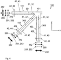
- Fig. 4 illustrates an example of a magnetic sensor device 100 for measuring a magnetic field direction, according to an embodiment.
- the magnetic sensor device 100 includes a plurality of the MLU cells 1.
- the configuration of the magnetic sensor device 100 of Fig. 4 is similar to the one described in Fig. 3 .
- the magnetic sensor device 100 comprises a plurality of branches 101, 102, 103 wherein each branch comprises a subset of the plurality of MLU cells 1 electrically connected in series to a current portion 301, 302, 303 of the current line 3, respectively.
- the magnetic sensor device 100 further comprises a programming line 4 configured for passing a programming field current 41 for inducing a programming magnetic field 42.
- the programming line comprises programming line portions 401, 402, 403, each programming line portions addressing a corresponding branch 101, 102, 103, respectively.
- each branch 101, 102, 103 includes an array comprising one or more rows and/or and columns of said plurality of MLU cells 1, electrically connected in series to one of the current lines 301, 302, 303.
- each branch 101, 102, 103 can comprise one row of MLU cells 1 or two or more adjacent rows of MLU cells 1.
- the programming field current 41 can be passed individually in each programming line portion 401, 402, 403.
- the programming line portions 401, 402, 403 can be electrically connected in series such that the programming field current 41 is simultaneously passed in the programming line portions 401, 402, 403.
- the magnetic sensor device 100 is represented having a first branch 101 oriented at angle of about 0° with respect to an axis x, a second branch 102 oriented at angle of about 45° and a third branch 103 oriented at angle of about 90° with respect to the axis x.
- a MLU cells comprised in the first, second and third branch 101, 102, 103 are addressed by a first, second and third programming line portion 401, 402, 403, respectively.
- the first, second and third programming line portions 401, 402, 403 are electrically connected in series such as to form a single programming line 4 in which the programming current 41 is passed.
- the programming line portions 401, 402, 403 are configured such that the programming field current 41 flowing in any of the programming line portion 401, 402, 403 induce the programming magnetic field 42 in a direction that is substantially perpendicular to the programming line portion 401, 402, 403 and to the branch 101, 102, 103.
- the magnetic sensor device 100 can comprise a plurality of branches such that the average storage magnetization directions 230 of the MLU cells 1 substantially equally spaced by an angle of about 360 degrees divided by "n", where "n" can be 8, or about 45°.
- a method for programming the magnetic sensor device 100 comprises the steps of:
- the storage magnetization 230 can be aligned in the programmed direction 260 by applying a programming magnetic field 42 in the field line 401, 402, 403.
- Inducing a storage stress-induced magnetic anisotropy 272 and/or a sense stress-induced magnetic anisotropy 271 can be performed by inducing a mechanical stress on the storage layer 23 and/or the sense layer 21.
- the mechanical stress can be induced by adapting the shape, the material properties and the fabrication conditions of the current line 3, the field line 4, the strap 7, or any other metallic line adapted for generating an appropriate mechanical stress.
- the mechanical stress can be induced by adapting the material properties and the fabrication conditions of insulating materials located at the vicinity the magnetic tunnel junction 2, such as a dielectric layer encapsulating the MLU cell 1.
- the stress inducing device 6 can be configured such that the direction of the storage induced magnetic anisotropy 271 is different for each of said plurality of branches 101, 102, 103. This can be achieved by orienting the current lines 301, 302, 303, or the field lines 401, 402, 403, the strap 7, or any other metallic line adapted for generating an appropriate mechanical stress, or insulating layer in the appropriate direction in each branch.
- the storage magnetization 230 of the MLU cells 1 comprised in each branch 101, 102, 103 can be aligned in a programmed direction 260 that is substantially parallel to the programming magnetic field 42.
- the programmed direction 260 of the storage magnetization 230 can be substantially parallel to the stress-induced magnetic anisotropy 272 of the storage layer 23 of the MLU cells 1 comprised in each branch 101, 102, 103.
- Fig. 4 also reports the orientation of the storage intrinsic anisotropy 251 for comparison.
- a direction of the sense stress-induced magnetic anisotropy 271 in the sense layer 21 and/or a direction of the storage stress-induced magnetic anisotropy 272 in the storage layer 23 can be adjusted by adjusting the amplitude of the applied anisotropic mechanical stress.
- the strength and the direction of the anisotropic mechanical stress is modified by adjusting at least one of the deposition conditions of the current line 3, 301, 302, 303, or the field line 4, 401, 402, 403, or the strap 7, or any other metallic line adapted for generating an appropriate mechanical stress, or insulating layers lying at the MLU cell 1 vicinity.
- the strength and the direction of the anisotropic mechanical stress can be further adjusted by a selection of a combination of materials having different thermal expansion coefficient for the metal and/or insulating materials forming the electrically stress-inducing device 6.
- the anisotropic mechanical stress applied by the stress inducing device 6 is between about 1 MPa to 5 GPa.
- the direction of the sense stress-induced magnetic anisotropy 271 in the sense layer 21 can be adjusted by modifying a sense magnetoelastic coupling constant ⁇ 1 of the sense layer 21.
- the direction of the storage stress-induced magnetic anisotropy 272 in the storage layer 23 can also be adjusted by modifying a storage magnetoelastic coupling constant ⁇ 2 of the storage layer 23.
- the sense magnetoelastic coupling constant ⁇ 1 and the storage magnetoelastic coupling constant ⁇ 2 have opposed signs. Applying the anisotropic mechanical stress thus results in the sense stress-induced magnetic anisotropy 271 of the sense layer 21 being oriented substantially perpendicular to the storage stress-induced magnetic anisotropy 272 of the storage layer 23.
- the sense magnetoelastic coupling constant ⁇ 1 and the storage magnetoelastic coupling constant ⁇ 2 is in the range between about -1000 ppm and about 1000 ppm.
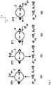
- Figs. 5a to 5d represent four possible ways to induce the sense stress-induced magnetic anisotropy 271 in the y direction by using the stress inducing device 6.
- the magnetic tunnel junction, or sense layer 21 is represented schematically viewed from the top.
- the sense stress-induced magnetic anisotropy 271 induced by stress ⁇ is perpendicular to the stress direction for compressive stress ( ⁇ xx > 0, see Fig. 5a ), and parallel to the stress direction for tensile stress ( ⁇ yy > 0, see Fig. 5d ).
- the sense stress-induced magnetic anisotropy 271 is perpendicular to the stress direction for tensile stress ( ⁇ xx > 0, see Fig. 5b ), or parallel to the stress direction for compressive stress ( ⁇ yy ⁇ 0, see Fig. 5c ).
- Figs. 6a to 6d represent four possible ways to induce a sense stress-induced magnetic anisotropy 271 in the sense layer 21 that is substantially perpendicular to the storage stress-induced magnetic anisotropy 272 in the storage layer 23 by using the stress inducing device 6.
- the magnetic tunnel junction 2 is represented schematically viewed from the top. This can be achieved by any combination of direction and sign of stress ⁇ , provided the sense magnetoelastic coupling constant ⁇ 1 and the storage magnetoelastic coupling constant ⁇ 2 have opposed signs.
- Figs. 6a to 6d represent four possible ways to induce a sense stress-induced magnetic anisotropy 271 in the sense layer 21 that is substantially perpendicular to the storage stress-induced magnetic anisotropy 272 in the storage layer 23 by using the stress inducing device 6.
- the magnetic tunnel junction 2 is represented schematically viewed from the top. This can be achieved by any combination of direction and sign of stress ⁇ , provided the sense magnetoelastic coupling constant ⁇ 1 and the
- a sense stress-induced magnetic anisotropy 271 in the sense layer 21 that is substantially perpendicular to the storage stress-induced magnetic anisotropy 272 in the storage layer 23 is achieved by applying a compressive stress ( ⁇ xx ⁇ 0) with the sense magnetoelastic coupling constant ⁇ 1 being negative ( ⁇ 0) and the storage magnetoelastic coupling constant ⁇ 2 being positive (> 0) ( Fig. 6a ). This is also achieved by applying a compressive stress ( ⁇ xx ⁇ 0) with ⁇ 1 > 0 and ⁇ 2 ⁇ 0 ( Fig.
- the stress inducing device 6 is thus capable of applying an anisotropic mechanical stress inducing the sense and storage stress-induced magnetic anisotropy 271, 272 on the sense layer 21 and the storage layer 23, respectively, with the sense stress-induced magnetic anisotropy 271 of the sense layer 21 having a direction that differs from a direction of the storage stress-induced magnetic anisotropy 272 of the storage layer 23.
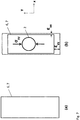
- Figs. 7a and 7b represent a way to induce anisotropic stress in the sense layer 21 and the storage layer 23 thanks to a metal line 7 having an appropriate shape and deposited at high temperature.
- the magnetic tunnel junction 2 and the stress-inducing device 6 are represented schematically viewed from the top.
- the stress-inducing device 6 comprises a metal line 7 having a rectangular shape (the longer dimension is along the y axis in that example).
- the metal line 7 is deposited at a temperature higher than the operating temperature of the sensor device ( Fig. 7a ).
- the operating temperature can vary between 0°C and 85°C, possibly between -40°C a 180°C and possibly up to 250°C.
- the deposition temperature can be between 150°C and 400°C and possibly between 20°C and 800°C.
- the metal line 7 cools after processing down to the operating temperature of the device. As it can be seen in Fig. 7b , the metal line 7 retracts due to the thermal retraction of the metal line 7 (the rectangle in dotted line show the dimensions of the line 7 prior to the cooling. Since the metal line 7 has a larger length (in y) than in width (in x), the retraction is anisotropic. In other words, the deformation ⁇ xx in the x direction is smaller than the deformation ⁇ yy in the y direction. The anisotropic retraction induces an anisotropic compressive stress in the y direction on the magnetic tunnel junction 2 that is deposited above the metal line 7.
- the method can further comprise the step of passing a heating current 31 in the current line 301, 302, 303 such as to heat the MLU cells 1 in the corresponding subset 101, 102, 103 at the high threshold temperature T H and unpin the storage magnetization 230 of said MLU cells 1.
- the method can comprise the step of cooling the MLU cells 1 comprised in the corresponding subset 101, 102, 103 to the low threshold temperature T L such as to pin the switching the storage magnetization 230 in the programmed direction 260.
- a sensing operation of the magnetic sensor device 100 comprises passing a sensing current 32 in the current branches 301, 302, 303 such as to measure an average resistance R.
- the average resistance R corresponds to the resistance measured in series for the MLU cells comprised in a branch 101, 102, 103.
- the resistance of each MLU cell is determined by the relative orientation of the sense magnetization 210 with respect to the storage magnetization 230.
- the sense magnetization 210 can be varied by passing a sense field current 43 in the programming line portions 401, 402, 403 such as to generate a sense magnetic field 44.
- the sense field current 43 can be alternated such as to modulate the sense magnetic field 44 and the average resistance R in accordance with the polarity of the sense field current 43.
- sense stress-induced magnetic anisotropy 271 (or sense net magnetic anisotropy 281)is initially substantially perpendicular to the storage stress-induced magnetic anisotropy 272 (or storage net magnetic anisotropy 282), the response will be linear.
- the sense magnetization 210 is aligned in the external magnetic field in accordance with the respective orientation of the external magnetic field and of the orientation of the branches 101, 102, 103 with respect to the direction of the external magnetic field.
- the external magnetic field can be determined by passing a sensing current 32 in the current branches 301, 302, 303 such as to measure an average resistance R by passing the sensing current 32 in the current branches 301, 302, 303.
- the MLU-based magnetic sensor device 100 disclosed herein may be included in, for example, a magnetometer and/or a compass.
- the magnetic sensor device 100 can be used for measuring a direction of an external magnetic field, such as the Earth's magnetic field, in two dimensions, e.g. a component of the external magnetic field in a two-dimensional plane.
- Devices incorporating design principles of the magnetic sensor device 100 may also measure a direction of the external magnetic field in three dimensions, such as by using the magnetic sensor device 100 with Hall effect vertical axis sensing.
- the Hall effect can result in a voltage difference (the Hall voltage) across an electrical conductor, transverse to an electric current in the conductor and a magnetic field perpendicular to the current. Based on the Hall effect, a component of the external magnetic field in the third dimension may be determined.
Landscapes
- Engineering & Computer Science (AREA)
- Computer Hardware Design (AREA)
- Physics & Mathematics (AREA)
- Condensed Matter Physics & Semiconductors (AREA)
- General Physics & Mathematics (AREA)
- Chemical & Material Sciences (AREA)
- Crystallography & Structural Chemistry (AREA)
- Power Engineering (AREA)
- Hall/Mr Elements (AREA)
- Mram Or Spin Memory Techniques (AREA)
- Measuring Magnetic Variables (AREA)
Description
- The present invention concerns a magnetic logic unit (MLU) - based magnetic sensor device for sensing an external magnetic field that can be easily programmed and that yield a linear signal when sensing the external magnetic field. The present disclosure further concerns a method for programming the magnetic sensor device.
- Magnetic logic unit (MLU) cells can be used to sense magnetic fields, in magnetic sensors or compasses. A MLU cell can comprise a magnetic tunnel junction including a storage layer having a storage magnetization, a sense layer having a sense magnetization and a tunnel barrier layer between the storage and sense layers. The sense magnetization is orientable in the presence of the external magnetic field while the storage magnetization remains substantially undisturbed by the external magnetic field. The external magnetic field can thus be sensed by measuring a resistance of the magnetic tunnel junction that depends on the relative orientation of the sense magnetization, oriented by the external magnetic field, and the storage magnetization.
- Ideally, the sense layer has a linear and non-hysteretic behavior when oriented by the external magnetic field in order to facilitate the measurement of small variations of the external magnetic field. That is relevant when sensing the earth's magnetic field having an average value on the order of 0.5 Oersted (Oe).
- Such linear and non-hysteretic behavior can be achieved by providing a magnetic tunnel junction where the sense magnetization magnetic anisotropy axis is oriented substantially perpendicular to the storage magnetization. This is usually achieved by pinning the storage magnetization perpendicular to an anisotropy axis of the sense layer. The orientation of the anisotropy axis of the sense layer can be defined by fabrication conditions, for example by applying a magnetic field, during the manufacturing of the magnetic tunnel junction.
- A drawback of the above MLU cell is that only one direction of anisotropy can be defined by the sputter conditions on a wafer comprising a plurality of MRAM cells. The
sense layer magnetization 210 can thus be oriented perpendicular to thestorage magnetization 230 in only one direction in the plane of the sensor device. -
Fig. 3 illustrates a conventional MLU-basedmagnetic sensor device 100 including a plurality of MLU cells electrically connected in series to acurrent line 3. A magnetic sensor usually requires at least two directions of sensing.Fig. 1 shows a conventional MLU cell comprising amagnetic tunnel junction 2 including asense layer 21 having asense magnetization 210, astorage layer 23 having astorage magnetization 230, a storageantiferromagnetic layer 24 pinning thestorage magnetization 230 at a low threshold temperature and freeing it at a high threshold temperature, and atunnel barrier layer 22. Thesense magnetization 210 is configured to be orientable in an external magnetic field such that a resistance of themagnetic tunnel junction 2, determined by the relative orientation of thesense magnetization 210 andstorage magnetization 230, is varied. - Referring back to
Fig. 3 the plurality of MLU cells is represented by thedotted patterns field line 4 is configured to generate a magnetic field based on an input (a field current). In particular, the plurality of MLU cells are configured inbranches portions branches field line portions current flow 41 through each of theportions corresponding branches magnetic field 42 is oriented in a direction perpendicular to the respectivefield line portion programming direction 260. The intrinsic anisotropy axis of thesense layer magnetization 210, referred as the sense intrinsic anisotropy axis 251 and the intrinsic anisotropy axis 252 of thestorage layer magnetization 230, referred as the storage intrinsic anisotropy axis 252 are defined by the sputter and/or annealing conditions. In absence of magnetic field, thesense magnetization 210 is oriented along the sense intrinsic anisotropy axis 251. InFig. 3 , the sense intrinsic anisotropy axis 251 and the storage intrinsic anisotropy axis 252 are oriented perpendicular to theprogrammed direction 260 in thebranches 101 at about 0°, at an angle of about 45° in thesubset 102 at about 45°, and substantially parallel to thestorage magnetization 230 in thesubset 103 at about 90°. - Another drawback of the conventional MLU-based magnetic sensor device is that during programming the device, i.e., during the step of setting the orientation of the storage magnetization, the
storage magnetization 230 can only be aligned in a direction being close to that of the storage intrinsic anisotropy axis 251. As discussed above, the latter is oriented in a single direction in all branches of the magnetic sensor device, the direction being determined by the fabrication process of the magnetic sensor device (sputter conditions, annealing conditions, etc.). The programming of the storage magnetization in a direction that is not close to the anisotropy axis requires a higher programming field than if the programming is performed in a direction that is close to the anisotropy axis. It is not possible in conventional MLU-based magnetic sensor devices to generate a programmingmagnetic field 42 with theprogramming line 4 that is large enough to program thestorage magnetization 230 in a direction that is not close to the anisotropy axis. - In order to obtain a 2D magnetic sensor device such as the one depicted in
Fig. 3 , thestorage layer 23 in theMLU cells 1 comprised in the different branches should be programmed in different directions and for some of the branches theprogramming direction 260 will be far from the magnetic anisotropy axis (i.e. there is an angle greater than 10° between theprogramming direction 260 and the magnetic anisotropy axis), resulting in a poor programming in these branches. The sensitivity of a poorly programmed branch to external magnetic fields is small, usually not large enough to determinate accurately the value of the external magnetic field. -
US2012075922 discloses a magnetic memory element capable of maintaining high thermal stability (retention characteristics) while reducing a writing current. The magnetic memory element includes a magnetic tunnel junction having a first magnetic body including a perpendicular magnetization film, an insulating layer, and a second magnetic body serving as a storage layer including a perpendicular magnetization film, which are sequentially stacked. A thermal expansion layer is disposed in contact with the magnetic tunnel junction portion. The second magnetic body is deformed in a direction in which the cross section thereof increases or decreases by the thermal expansion or contraction of the thermal expansion layer due to the flow of a current, thereby reducing a switching current threshold value required to change the magnetization direction. -
US2010080048 discloses a magnetic memory cell including a piezoelectric material, and methods of operating the memory cell are provided. The memory cell includes a stack, and the piezoelectric material may be formed as a layer in the stack or adjacent the layers of the cell stack. The piezoelectric material may be used to induce a transient stress during programming of the memory cell to reduce the critical switching current of the memory cell. -
US2002117727 discloses a magnetoelectronics element that is comprised of a first magnetic layer, a first tunnel barrier layer on the first magnetic layer, a second magnetic layer on the first tunnel barrier layer and a stressed over-layer on said second magnetic layer, which is configured to alter a switching energy barrier of said second magnetic layer. - The present disclosure concerns a magnetic sensor device according to
claim 1. - The present disclosure further concerns a method for programming the magnetic sensor according to claim 13.
- An advantage of the disclosed magnetic sensor device is that the magnetic anisotropy of the sense and storage layers can be oriented in a specific direction for each branch and each layer, such that the programming as well as the sensitivity of each branch, and thus the magnetic sensor device, will be improved. Indeed, each branch is easier to program due to the net magnetic anisotropy of the storage layer being oriented in a direction close to that of the programmed direction. Since the magnetization of the sense layer is oriented perpendicular to the storage layer magnetization, each branch of the magnetic sensor device presents a linear and non-hysteretic behaviour.
- The invention will be better understood with the aid of the description of an embodiment given by way of example and illustrated by the figures, in which:
-
Fig. 1 represents a magnetic tunnel junction comprising a storage layer, a tunnel barrier layer and a sense layer; -
Fig. 2 represents the magnetic tunnel junction ofFig. 1 where the storage layer is a synthetic antiferromagnet comprising a first storage ferromagnetic layer, a second storage ferromagnetic layer and an anti-parallel coupling layer; -
Fig. 3 illustrates a conventional MLU-based magnetic sensor comprising a first, second and third branch comprising MLU cells; -
Fig. 4 illustrates a MLU-based magnetic field direction measurement device, according to an embodiment: -
Figs. 5a to 5d illustrate four possible ways to induce a stress-induced magnetic anisotropy in the y direction by using the stress inducing device; -
Figs. 6a to 6d represent four possible ways to induce a stress-induced magnetic anisotropy in the sense layer that is substantially perpendicular to the stress-induced magnetic anisotropy in the storage layer by using the stress inducing device; and -
Figs. 7a and 7b represent a way to induce anisotropic stress in the sense layer and the storage layer thanks to a metal line having an appropriate shape and deposited at high temperature. - Referring to
Fig. 1 , aMLU cell 1 for sensing an external magnetic field comprises amagnetic tunnel junction 2 including asense layer 21, astorage layer 23 and atunnel barrier layer 22 between thesense layer 21 and thestorage layer 23. Thesense layer 21 has asense magnetization 210 that is freely orientable in the external magnetic field. Thestorage layer 23 has astorage magnetization 230 which orientation remains stable in the external magnetic field. TheMLU cell 1 can further include traces or strip conductors to provide write and read functionality. Specifically, acurrent line 3 can be electrically coupled to theMLU cell 1. TheMLU cell 1 can include aprogramming line 4 extending substantially perpendicular (or parallel) to thecurrent line 3 and being magnetically coupled to theMLU cell 1. TheMLU cell 1 can further include a selection transistor 8 electrically connected, through a strap 7, to theMLU cell 1. - The
sense layer 21 can include a soft ferromagnetic material, namely one having a relatively low magnetic anisotropy, while thestorage layer 23 can include a hard ferromagnetic material, namely one having a relatively high coercivity. Suitable ferromagnetic materials include transition metals, rare earth elements, and their alloys, either with or without main group elements. For example, suitable ferromagnetic materials include iron ("Fe"), cobalt ("Co"), nickel ("Ni"), and their alloys, such as permalloy (or Ni80Fe20); alloys based on Ni, Fe, and boron ("B"); Co90Fe10; and alloys based on Co, Fe, and B. A thickness of each of thesense layer 21 and thestorage layer 23 can be in the nm range, such as from about 0.4 nm to about 20 nm or from about 1 nm to about 10 nm. - Other implementations of the
sense layer 21 and thestorage layer 23 are contemplated. For example, either, or both, of thesense layer 21 and thestorage layer 23 can include multiple sub-layers in a fashion similar to that of the so-called synthetic antiferromagnetic layer.Fig. 2 shows themagnetic tunnel junction 2 where thestorage layer 23 includes a synthetic storage layer, or synthetic antiferromagnet (SAF), comprising a first storageferromagnetic layer 231 having afirst storage magnetization 234, and a second storageferromagnetic layer 232 having asecond storage magnetization 235. A storageanti-parallel coupling layer 233 is included between the first and second storageferromagnetic layers storage coupling layer 233 produces a RKKY coupling between the first and second storage layers 231, 232 such that thesecond storage magnetization 235 remains antiparallel to thefirst storage magnetization 234. The two storageferromagnetic layers storage coupling layer 233 can comprise a non-magnetic material selected from a group comprising at least one of: ruthenium, chromium, rhenium, iridium, rhodium, silver, copper and yttrium. Preferably, thestorage coupling layer 233 comprises ruthenium and has a thickness typically included between about 0.4 nm and 3nm, preferably between 0.6nm and about 0.9 nm or between about 1.6nm and about 2nm. - The
tunnel barrier layer 22 can include, or can be formed of, an insulating material. Suitable insulating materials include oxides, such as aluminum oxide (e.g., Al2O3) and magnesium oxide (e.g., MgO). A thickness of thetunnel barrier layer 22 can be in the nm range, such as from about 0.5 nm to about 10 nm. - The
MLU cell 1 can be configured to be written, or programmed, by a thermally-assisted switching (TAS) operation. Again referring toFig. 1 , theMLU cell 1 can further include a pinninglayer 24, which is disposed adjacent to thestorage layer 23 and, through exchange bias, stabilizes, or pin, thestorage magnetization 230 along a particular direction when a temperature within, or in the vicinity of, the pinninglayer 24 is at a low threshold temperature TL. The low threshold temperature TL can correspond to a temperature being below a blocking temperature, a Neel temperature, or another threshold temperature. The pinninglayer 24 unpins, or decouples, thestorage magnetization 230 when the temperature is at high threshold temperature TH, i.e., at a temperature above the blocking temperature, thereby allowing thestorage magnetization 230 to be switched to another direction. - As illustrated in
Fig. 2 , in the case the storage layer has a SAF configuration, the pinninglayer 24 can be adjacent to the first storageferromagnetic layer 231 such as to pin thefirst storage magnetization 234 at the low threshold temperature TL and free it at the at high threshold temperature TH. Thesecond storage magnetization 235 is not exchange coupled by the pinninglayer 24 but remains anti-parallel coupled to thefirst storage magnetization 234 through thestorage coupling layer 233. The pinninglayer 24 could also be adjacent to the second storageferromagnetic layer 232 such as to exchange couple this layer. - The pinning
layer 24 includes, or is formed of, a magnetic material and, in particular, a magnetic material of the antiferromagnetic type. Suitable antiferromagnetic materials include transition metals and their alloys. For example, suitable antiferromagnetic materials include alloys based on manganese ("Mn"), such as alloys based on iridium ("Ir") and Mn (e.g., IrMn); alloys based on Fe and Mn (e.g., FeMn); alloys based on platinum ("Pt") and Mn (e.g., PtMn); and alloys based on Ni and Mn (e.g., NiMn). In some instances, the blocking temperature of alloys based on Ir and Mn (or based on Fe and Mn) can be in the range of about 90°C to about 350°C or about 150°C to about 200°C, and can be smaller than the blocking temperature of alloys based on Pt and Mn (or based on Ni and Mn), which can be in the range of about 200°C to about 400°C. - In an embodiment, the
MLU cell 1 comprises a stress inducing device 6 configured for applying an anisotropic mechanical stress on themagnetic tunnel junction 2 such as to induce a stress-induced magnetic anisotropy 270 on at least one of thesense layer 21 and thestorage layer 23. - A magnetostrictive material develops large mechanical deformations when subjected to an external magnetic field. This phenomenon is attributed to the rotations of small magnetic domains in the material, which are randomly oriented when the material is not exposed to a magnetic field. The orientation of these small domains by the imposition of the magnetic field creates a strain field. As the intensity of the magnetic field is increased, more and more magnetic domains orientate themselves so that their principal axes of anisotropy are collinear with the magnetic field in each region and finally saturation is achieved. Conversely, the change in magnetization or magnetic anisotropy axis due to applied stress is also known as magnetoelastic effect or Villari effect.
- Thus, applying an anisotropic mechanical stress on the
magnetic tunnel junction 2 induces an additional magnetic anisotropy source, referred as stress induced magnetic anisotropy. Such anisotropic mechanical stress is generated by the stress inducing device 6. The stress inducing device 6 can comprise metal lines or an oxide located at the vicinity of themagnetic tunnel junction 2. In an embodiment, the stress inducing device 6 comprises thecurrent line 3 and / or theprogramming line 4. Alternatively, or in combination, the stress inducing device 6 can comprise an additional metallic line, such as the strap 7, or any other metallic line adapted for generating an appropriate mechanical stress. Alternatively, or in combination, the stress inducing device 6 can comprise an encapsulation layer (not shown), such as a dielectric layer encapsulating theMLU cell 1. - The stress inducing device is further configured such that the stress-induced magnetic anisotropy 270 has a larger magnitude that any other possible contributions of magnetic anisotropy, (thereafter referred as sense intrinsic anisotropy 251 for the
sense layer 21 and storage intrinsic anisotropy 252 for thestorage layer 23 in the following text) such as magnetic anisotropy induced by deposition and or annealing, shape or crystalline anisotropy. The stress-induced magnetic anisotropy in thesense layer 21 will be referred as sense stress-inducedmagnetic anisotropy 271, and the stress-induced magnetic anisotropy in thestorage layer 23 will be referred as storage stress-inducedmagnetic anisotropy 272. The stress inducing device 6 is thus configured such that the sense stress-inducedmagnetic anisotropy 271 corresponds substantially to a net sense magnetic anisotropy 281, and the storage stress-inducedmagnetic anisotropy 272 corresponds substantially to a net storage magnetic anisotropy 282 (seeFig. 4 ). Here, the net sense magnetic anisotropy 281 corresponds to the sum of the sense intrinsic anisotropy 251 and the sense stress-inducedmagnetic anisotropy 271 and the net storagemagnetic anisotropy 282 corresponds to the sum of the storage intrinsic anisotropy 251 and the storage stress-inducedmagnetic anisotropy 271. In other words, the sense intrinsic anisotropy 251 can be neglected compared to the sense stress-inducedmagnetic anisotropy 271 and the storage intrinsic anisotropy 252 can be neglected compared to the storage stress-inducedmagnetic anisotropy 272 -
Fig. 4 illustrates an example of amagnetic sensor device 100 for measuring a magnetic field direction, according to an embodiment. Themagnetic sensor device 100 includes a plurality of theMLU cells 1. The configuration of themagnetic sensor device 100 ofFig. 4 is similar to the one described inFig. 3 . Themagnetic sensor device 100 comprises a plurality ofbranches MLU cells 1 electrically connected in series to acurrent portion current line 3, respectively. Themagnetic sensor device 100 further comprises aprogramming line 4 configured for passing a programming field current 41 for inducing a programmingmagnetic field 42. The programming line comprisesprogramming line portions corresponding branch - More particularly, each
branch MLU cells 1, electrically connected in series to one of thecurrent lines branch MLU cells 1 or two or more adjacent rows ofMLU cells 1. The programming field current 41 can be passed individually in eachprogramming line portion programming line portions programming line portions - In the arrangement of
Fig. 4 , themagnetic sensor device 100 is represented having afirst branch 101 oriented at angle of about 0° with respect to an axis x, asecond branch 102 oriented at angle of about 45° and athird branch 103 oriented at angle of about 90° with respect to the axis x. A MLU cells comprised in the first, second andthird branch programming line portion programming line portions single programming line 4 in which the programming current 41 is passed. - The
programming line portions programming line portion magnetic field 42 in a direction that is substantially perpendicular to theprogramming line portion branch - Other configurations of the
magnetic sensor device 100 can be contemplated. For example, themagnetic sensor device 100 can comprise a plurality of branches such that the averagestorage magnetization directions 230 of theMLU cells 1 substantially equally spaced by an angle of about 360 degrees divided by "n", where "n" can be 8, or about 45°. - According to an embodiment, a method for programming the
magnetic sensor device 100, comprises the steps of: - using the stress inducing device 6 for inducing a storage stress-induced
magnetic anisotropy 272 on thestorage layer 23 such that the storage stress-inducedmagnetic anisotropy 272 of thestorage layer 23 is substantially parallel to the programmingmagnetic field 42; and - aligning the
storage magnetization 230 of theMLU cells 1 comprised in each subset in a programmed direction 260 (seeFig. 4 ) that is substantially parallel to the programmingmagnetic field 42. - The
storage magnetization 230 can be aligned in theprogrammed direction 260 by applying a programmingmagnetic field 42 in thefield line - Inducing a storage stress-induced
magnetic anisotropy 272 and/or a sense stress-inducedmagnetic anisotropy 271 can be performed by inducing a mechanical stress on thestorage layer 23 and/or thesense layer 21. The mechanical stress can be induced by adapting the shape, the material properties and the fabrication conditions of thecurrent line 3, thefield line 4, the strap 7, or any other metallic line adapted for generating an appropriate mechanical stress. Alternatively, or in combination, the mechanical stress can be induced by adapting the material properties and the fabrication conditions of insulating materials located at the vicinity themagnetic tunnel junction 2, such as a dielectric layer encapsulating theMLU cell 1. - In an embodiment, the stress inducing device 6 can be configured such that the direction of the storage induced
magnetic anisotropy 271 is different for each of said plurality ofbranches current lines field lines - During the programming operation, the
storage magnetization 230 of theMLU cells 1 comprised in eachbranch programmed direction 260 that is substantially parallel to the programmingmagnetic field 42. Thus, theprogrammed direction 260 of thestorage magnetization 230 can be substantially parallel to the stress-inducedmagnetic anisotropy 272 of thestorage layer 23 of theMLU cells 1 comprised in eachbranch Fig. 4 also reports the orientation of the storage intrinsic anisotropy 251 for comparison. - In an embodiment, a direction of the sense stress-induced
magnetic anisotropy 271 in thesense layer 21 and/or a direction of the storage stress-inducedmagnetic anisotropy 272 in thestorage layer 23 can be adjusted by adjusting the amplitude of the applied anisotropic mechanical stress. - In another embodiment, the strength and the direction of the anisotropic mechanical stress is modified by adjusting at least one of the deposition conditions of the
current line field line MLU cell 1 vicinity. The strength and the direction of the anisotropic mechanical stress can be further adjusted by a selection of a combination of materials having different thermal expansion coefficient for the metal and/or insulating materials forming the electrically stress-inducing device 6. - In an embodiment, the anisotropic mechanical stress applied by the stress inducing device 6 is between about 1 MPa to 5 GPa.
- The direction of the sense stress-induced
magnetic anisotropy 271 in thesense layer 21 can be adjusted by modifying a sense magnetoelastic coupling constant λ1 of thesense layer 21. The direction of the storage stress-inducedmagnetic anisotropy 272 in thestorage layer 23 can also be adjusted by modifying a storage magnetoelastic coupling constant λ2 of thestorage layer 23. - In an embodiment, the sense magnetoelastic coupling constant λ1 and the storage magnetoelastic coupling constant λ2 have opposed signs. Applying the anisotropic mechanical stress thus results in the sense stress-induced
magnetic anisotropy 271 of thesense layer 21 being oriented substantially perpendicular to the storage stress-inducedmagnetic anisotropy 272 of thestorage layer 23. In a particular arrangement, the sense magnetoelastic coupling constant λ1 and the storage magnetoelastic coupling constant λ2 is in the range between about -1000 ppm and about 1000 ppm. -
Figs. 5a to 5d represent four possible ways to induce the sense stress-inducedmagnetic anisotropy 271 in the y direction by using the stress inducing device 6. InFigs. 5a to 5d , the magnetic tunnel junction, orsense layer 21, is represented schematically viewed from the top. For a positive sense magnetoelastic coupling constant λ1, the sense stress-inducedmagnetic anisotropy 271 induced by stress σ is perpendicular to the stress direction for compressive stress (σxx > 0, seeFig. 5a ), and parallel to the stress direction for tensile stress (σyy > 0, seeFig. 5d ). For a negative sense magnetoelastic coupling constant λ1, the sense stress-inducedmagnetic anisotropy 271 is perpendicular to the stress direction for tensile stress (σxx > 0, seeFig. 5b ), or parallel to the stress direction for compressive stress (σyy < 0, seeFig. 5c ). -
Figs. 6a to 6d represent four possible ways to induce a sense stress-inducedmagnetic anisotropy 271 in thesense layer 21 that is substantially perpendicular to the storage stress-inducedmagnetic anisotropy 272 in thestorage layer 23 by using the stress inducing device 6. InFigs. 6a to 6d , themagnetic tunnel junction 2, is represented schematically viewed from the top. This can be achieved by any combination of direction and sign of stress σ, provided the sense magnetoelastic coupling constant λ1 and the storage magnetoelastic coupling constant λ2 have opposed signs. In the example ofFigs. 6a to 6d , a sense stress-inducedmagnetic anisotropy 271 in thesense layer 21 that is substantially perpendicular to the storage stress-inducedmagnetic anisotropy 272 in thestorage layer 23 is achieved by applying a compressive stress (σxx < 0) with the sense magnetoelastic coupling constant λ1 being negative (< 0) and the storage magnetoelastic coupling constant λ2 being positive (> 0) (Fig. 6a ). This is also achieved by applying a compressive stress (σxx < 0) with λ1 > 0 and λ2 < 0 (Fig. 6b ); or by applying a tensile stress (σxx > 0) with λ1 < 0 and λ2 > 0 (Fig. 6c ); and by applying a tensile stress (σxx > 0) with λ1 > 0 and λ2 < 0 (Fig. 6d ). - The stress inducing device 6 is thus capable of applying an anisotropic mechanical stress inducing the sense and storage stress-induced
magnetic anisotropy sense layer 21 and thestorage layer 23, respectively, with the sense stress-inducedmagnetic anisotropy 271 of thesense layer 21 having a direction that differs from a direction of the storage stress-inducedmagnetic anisotropy 272 of thestorage layer 23. -
Figs. 7a and 7b represent a way to induce anisotropic stress in thesense layer 21 and thestorage layer 23 thanks to a metal line 7 having an appropriate shape and deposited at high temperature. InFigs. 7a and 7b , themagnetic tunnel junction 2 and the stress-inducing device 6 are represented schematically viewed from the top. In the present example, the stress-inducing device 6 comprises a metal line 7 having a rectangular shape (the longer dimension is along the y axis in that example). The metal line 7 is deposited at a temperature higher than the operating temperature of the sensor device (Fig. 7a ). The operating temperature can vary between 0°C and 85°C, possibly between -40°C a 180°C and possibly up to 250°C. The deposition temperature can be between 150°C and 400°C and possibly between 20°C and 800°C. The metal line 7 cools after processing down to the operating temperature of the device. As it can be seen inFig. 7b , the metal line 7 retracts due to the thermal retraction of the metal line 7 (the rectangle in dotted line show the dimensions of the line 7 prior to the cooling. Since the metal line 7 has a larger length (in y) than in width (in x), the retraction is anisotropic. In other words, the deformation εxx in the x direction is smaller than the deformation εyy in the y direction. The anisotropic retraction induces an anisotropic compressive stress in the y direction on themagnetic tunnel junction 2 that is deposited above the metal line 7. - In the case of a TAS-based programming operation, the method can further comprise the step of passing a heating current 31 in the
current line MLU cells 1 in thecorresponding subset storage magnetization 230 of saidMLU cells 1. After, or simultaneously with the step of aligning thestorage magnetization 230 in theprogrammed direction 260, the method can comprise the step of cooling theMLU cells 1 comprised in thecorresponding subset storage magnetization 230 in theprogrammed direction 260. - A sensing operation of the
magnetic sensor device 100 comprises passing a sensing current 32 in thecurrent branches branch sense magnetization 210 with respect to thestorage magnetization 230. Thesense magnetization 210 can be varied by passing a sense field current 43 in theprogramming line portions - When the
magnetic sensor device 100 is used for sensing an external magnetic field, such as the earth magnetic field, thesense magnetization 210 is aligned in the external magnetic field in accordance with the respective orientation of the external magnetic field and of the orientation of thebranches current branches current branches - The MLU-based
magnetic sensor device 100 disclosed herein may be included in, for example, a magnetometer and/or a compass. - In one embodiment, the
magnetic sensor device 100 can be used for measuring a direction of an external magnetic field, such as the Earth's magnetic field, in two dimensions, e.g. a component of the external magnetic field in a two-dimensional plane. Devices incorporating design principles of themagnetic sensor device 100 may also measure a direction of the external magnetic field in three dimensions, such as by using themagnetic sensor device 100 with Hall effect vertical axis sensing. The Hall effect can result in a voltage difference (the Hall voltage) across an electrical conductor, transverse to an electric current in the conductor and a magnetic field perpendicular to the current. Based on the Hall effect, a component of the external magnetic field in the third dimension may be determined. -
- 1
- MLU cell
- 100
- magnetic sensor device
- 101
- first subset, first branch
- 102
- second subset, second branch
- 103
- third subset, third branch
- 2
- magnetic tunnel junction
- 21
- sense layer
- 210
- sense magnetization
- 22
- tunnel barrier layer
- 23
- storage layer
- 230
- storage magnetization
- 231
- first storage ferromagnetic layer
- 232
- second storage ferromagnetic layer
- 233
- storage coupling layer
- 234
- first storage magnetization
- 235
- second storage magnetization
- 24
- pinning layer
- 251
- sense intrinsic anisotropy
- 252
- storage intrinsic anisotropy
- 260
- programmed direction
- 271
- sense stress-induced magnetic anisotropy
- 272
- storage stress-induced magnetic anisotropy
- 281
- sense net magnetic anisotropy
- 282
- storage net magnetic anisotropy
- 3
- current line
- 301
- first current branch
- 302
- second current branch
- 303
- third current branch
- 31
- heating current
- 32
- sense current
- 4
- programming line
- 401
- programming line portion
- 402
- programming line portion
- 403
- programming line portion
- 41
- programming field current
- 42
- programming magnetic field
- 43
- sense field current
- 44
- sense magnetic field
- 6
- stress-inducing device
- 7
- additional metal line
- λ1
- sense magnetoelastic coupling constant
- λ2
- storage magnetoelastic coupling constant
- σ
- stress
- ε
- deformation
- σxx
- stress in the x direction
- σyy
- stress in the y direction
- εxx
- deformation in the x direction
- εyy
- deformation in the y direction
- R
- average resistance
- TH
- high threshold temperature
- TL
- low threshold temperature
Claims (14)
- A magnetic sensor device (100) for sensing an external magnetic field, comprising a plurality of magnetic logic unit, MLU, cells (1), each MLU cell (1) comprising a magnetic tunnel junction (2) including a sense layer (21) having a sense magnetization (210) freely orientable in the external magnetic field; a storage layer (23) having a storage magnetization (230); and a tunnel barrier layer (22) between the sense layer (21) and the storage layer (23);
wherein,the magnetic sensor device (100) further comprises a stress inducing device (6) configured for applying an anisotropic mechanical stress on the magnetic tunnel junction (2) such as to induce a stress-induced magnetic anisotropy (271, 272) on at least one of the sense layer (21) and the storage layer (23); and
in that the stress-induced magnetic anisotropy (271, 272) induced by the stress inducing device (6) corresponds substantially to a net magnetic anisotropy (281, 282) of said at least one of the sense layer (21) and the storage layer (23)
characterized in that
the stress inducing device (6) is further configured such that the applied anisotropic mechanical stress induces the stress-induced magnetic anisotropy (271, 272) in the sense and storage layers (21, 23), such that a direction of the sense stress-induced magnetic anisotropy (271) of the sense layer (21) differs from a direction of the storage stress-induced magnetic anisotropy (272) of the storage layer (23). - The magnetic sensor device (100) according to claim 1,
wherein the respective directions of the stress-induced magnetic anisotropy (271, 272) of the sense and storage layers (21, 23) is adjustable by adjusting the amplitude of the applied anisotropic mechanical stress. - The magnetic sensor device (100) according to claim 1 or 2,
wherein the direction of a sense stress-induced magnetic anisotropy (271) of the sense layer (21) is adjustable by adjusting a sense magnetoelastic coupling constant (λ1) of the sense layer (21) and
wherein the direction of a storage stress-induced magnetic anisotropy (272) of the storage layer (23) is adjustable by adjusting a storage magnetoelastic coupling constant (λ2) of the storage layer (23). - The magnetic sensor device (100) according to claim 3,
wherein the sense magnetoelastic coupling constant (λ1) has a sign being opposed to the one of the storage magnetoelastic coupling constant (λ2), such that, when the anisotropic mechanical stress is applied, the sense stress-induced magnetic anisotropy (271) of the sense layer (21) is oriented substantially perpendicular to the storage stress-induced magnetic anisotropy (272) of the storage layer (23). - The magnetic sensor device (100) according to claim 3 or 4,
wherein the sense magnetoelastic coupling constant (λ1) and the storage magnetoelastic coupling constant (λ2) is in the range between - 1000 ppm and 1000 ppm. - The magnetic sensor device (100) according to any one of claims 1 to 5,
wherein the stress inducing device (6) comprises an electrically conductive
strip comprising a metal (3, 4, 7) and/or an insulating material adapted for inducing the stress-induced anisotropic mechanical stress. - The magnetic sensor device (100) according to claim 6,
wherein the strength and the direction of the anisotropic stress is adjustable by adjusting at least one of: the nature of the material and the deposition conditions of the metal line (3, 4, 7) and/or oxide forming the stress-inducing device (6), or the shape of the metal line (3, 4, 7). - The magnetic sensor device (100) according to any one of claims 6 or 7,
wherein the strength and the direction of the anisotropic stress is adjustable by selecting a combination of materials having different thermal expansion coefficient for the metal and/or oxide forming stress-inducing device (6). - The magnetic sensor device (100) according to any one of claims 1 to 8,
wherein the anisotropic mechanical stress applied by the stress inducing device (6) is between about 1 MPa to 5 GPa. - The magnetic sensor device (100) according to any one of claims 1 to 9, comprising:a plurality of branches (101, 102, 103), each branch comprising a subset of a plurality of MLU cells (1), each subset being electrically connected in series by a current line (301, 302, 303) configured for passing a sense current (311, 312, 313) adapted for sensing an average resistance of the subset corresponding to an average orientation of the sense magnetization (210) in each of said plurality of MLU cells (1), in response to the external magnetic field;wherein the stress inducing device (6) is configured for inducing the stress-induced magnetic anisotropy (271, 272) on at least one of the sense layer (21) and the storage layer (23) of each MLU cell (1) of the subset, for each of said plurality of branches (101, 102, 103).
- The magnetic sensor device (100) according to claim 10,
wherein each subset being in magnetic communication with a programming line (401, 402, 403) arranged for passing a field current (41) inducing a programming magnetic field (42) adapted for aligning the storage magnetization (230) of the MLU cells (1) comprised in the subset in a programmed direction; - The magnetic sensor device (100) according to claim 10 or 11, wherein the stress inducing device (6) is further configured such that the direction of the induced magnetic anisotropy (271, 272) is different for each of said plurality of branches (101, 102, 103).
- A method for programming the magnetic sensor device (100) according to any one of claims 1 to 12, comprising:using the stress inducing device (6) for inducing a stress-induced magnetic anisotropy (271, 272) on the sense layer (21) and the storage layer (23) such that a direction of the sense stress-induced magnetic anisotropy (271) of the sense layer (21) differs from a direction of the storage stress-induced magnetic anisotropy (272) of the storage layer (23); andaligning the storage magnetization (230) of each of said plurality of MLU cells (1) in a programmed direction (260).
- The method according to claim 13, for the magnetic sensor device (100) according to any one of claims 10 to 12
wherein said aligning the storage magnetization (230) is performed for each branch (101, 102, 103) for the MLU cells (1) comprised in each subset.
Priority Applications (5)
| Application Number | Priority Date | Filing Date | Title |
|---|---|---|---|
| EP15290013.0A EP3045927B1 (en) | 2015-01-16 | 2015-01-16 | Mlu based magnetic sensor having improved programmability and sensitivity |
| PCT/IB2015/059917 WO2016113618A1 (en) | 2015-01-16 | 2015-12-23 | Mlu based magnetic sensor having improved programmability and sensitivity |
| US15/543,614 US9995798B2 (en) | 2015-01-16 | 2015-12-23 | MLU based magnetic sensor having improved programmability and sensitivity |
| CN201580073510.4A CN107110921B (en) | 2015-01-16 | 2015-12-23 | MLU-based magnetic sensor with improved programmability and sensitivity |
| JP2017537501A JP6864623B2 (en) | 2015-01-16 | 2015-12-23 | MLU-based magnetic sensor with improved programmability and sensitivity |
Applications Claiming Priority (1)
| Application Number | Priority Date | Filing Date | Title |
|---|---|---|---|
| EP15290013.0A EP3045927B1 (en) | 2015-01-16 | 2015-01-16 | Mlu based magnetic sensor having improved programmability and sensitivity |
Publications (2)
| Publication Number | Publication Date |
|---|---|
| EP3045927A1 EP3045927A1 (en) | 2016-07-20 |
| EP3045927B1 true EP3045927B1 (en) | 2017-12-20 |
Family
ID=53267276
Family Applications (1)
| Application Number | Title | Priority Date | Filing Date |
|---|---|---|---|
| EP15290013.0A Active EP3045927B1 (en) | 2015-01-16 | 2015-01-16 | Mlu based magnetic sensor having improved programmability and sensitivity |
Country Status (5)
| Country | Link |
|---|---|
| US (1) | US9995798B2 (en) |
| EP (1) | EP3045927B1 (en) |
| JP (1) | JP6864623B2 (en) |
| CN (1) | CN107110921B (en) |
| WO (1) | WO2016113618A1 (en) |
Families Citing this family (4)
| Publication number | Priority date | Publication date | Assignee | Title |
|---|---|---|---|---|
| JP6722304B2 (en) * | 2017-02-20 | 2020-07-15 | 株式会社村田製作所 | Stress sensor |
| WO2021250924A1 (en) * | 2020-06-11 | 2021-12-16 | 株式会社村田製作所 | Magnetic sensor chip and magnetic sensor device |
| CN114062978B (en) * | 2021-11-15 | 2024-02-02 | 东南大学 | MEMS magnetic field sensor based on piezoelectric tunneling effect and magnetic field measuring method |
| WO2023190993A1 (en) * | 2022-03-30 | 2023-10-05 | 日東電工株式会社 | Magnetic thin film-equipped substrate, magnetic thermoelectric conversion element, sensor, and method for manufacturing magnetic thin film-equipped substrate |
Family Cites Families (7)
| Publication number | Priority date | Publication date | Assignee | Title |
|---|---|---|---|---|
| US6515341B2 (en) * | 2001-02-26 | 2003-02-04 | Motorola, Inc. | Magnetoelectronics element having a stressed over-layer configured for alteration of the switching energy barrier |
| FR2852399B1 (en) * | 2003-03-14 | 2005-07-15 | Roulements Soc Nouvelle | MAGNETORIESISTIVE SENSOR COMPRISING A FERROMAGNETIC / ANTIFERROMAGNETIC SENSITIVE ELEMENT |
| US7582923B2 (en) * | 2004-11-16 | 2009-09-01 | Nec Corporation | Magnetic memory and manufacturing method for the same |
| US8310861B2 (en) * | 2008-09-30 | 2012-11-13 | Micron Technology, Inc. | STT-MRAM cell structure incorporating piezoelectric stress material |
| WO2010134378A1 (en) * | 2009-05-19 | 2010-11-25 | 富士電機ホールディングス株式会社 | Magnetic memory element and storage device using same |
| US8704320B2 (en) * | 2011-09-12 | 2014-04-22 | Qualcomm Incorporated | Strain induced reduction of switching current in spin-transfer torque switching devices |
| EP2608208B1 (en) * | 2011-12-22 | 2015-02-11 | Crocus Technology S.A. | Self-referenced MRAM cell and method for writing the cell using a spin transfer torque write operation |
-
2015
- 2015-01-16 EP EP15290013.0A patent/EP3045927B1/en active Active
- 2015-12-23 US US15/543,614 patent/US9995798B2/en active Active
- 2015-12-23 CN CN201580073510.4A patent/CN107110921B/en not_active Expired - Fee Related
- 2015-12-23 WO PCT/IB2015/059917 patent/WO2016113618A1/en active Application Filing
- 2015-12-23 JP JP2017537501A patent/JP6864623B2/en active Active
Non-Patent Citations (1)
| Title |
|---|
| None * |
Also Published As
| Publication number | Publication date |
|---|---|
| CN107110921A (en) | 2017-08-29 |
| CN107110921B (en) | 2020-02-07 |
| US20180003781A1 (en) | 2018-01-04 |
| JP2018503824A (en) | 2018-02-08 |
| JP6864623B2 (en) | 2021-04-28 |
| US9995798B2 (en) | 2018-06-12 |
| WO2016113618A1 (en) | 2016-07-21 |
| EP3045927A1 (en) | 2016-07-20 |
Similar Documents
| Publication | Publication Date | Title |
|---|---|---|
| US9983275B2 (en) | Method for measuring three-dimensional magnetic fields | |
| EP2860543B1 (en) | Magnetic sensor cell for measuring three-dimensional magnetic fields | |
| JP2013093558A (en) | Magnetic random access memory (mram) cell and method for writing and reading mram cell by using self reference read operation | |
| US9995798B2 (en) | MLU based magnetic sensor having improved programmability and sensitivity | |
| US10191719B2 (en) | MRAM-based programmable magnetic device for generating random numbers | |
| EP2528060A1 (en) | Multibit cell with synthetic storage layer | |
| US9905283B2 (en) | Self-referenced MRAM cell and magnetic field sensor comprising the self-referenced MRAM cell | |
| US9679624B2 (en) | Magnetic random access memory (MRAM) cell with low power consumption | |
| US9305628B2 (en) | Self-referenced magnetic random access memory (MRAM) and method for writing to the MRAM cell with increased reliability and reduced power consumption | |
| US10330749B2 (en) | Magnetic logic unit (MLU) cell for sensing magnetic fields with improved programmability and low reading consumption | |
| US10712399B2 (en) | MLU cell for sensing an external magnetic field and a magnetic sensor device comprising the MLU cell | |
| EP3115994B1 (en) | Magnetic memory device that is protected against reading using an external magnetic field and method for operating such magnetic memory device | |
| EP2958108B1 (en) | Self-referenced multibit MRAM cell having a synthetic antiferromagnetic storage layer | |
| EP4231031A1 (en) | Magnetoresistive element having thermally robust performances after high-field exposure and sensor comprising the magnetoresistive element |
Legal Events
| Date | Code | Title | Description |
|---|---|---|---|
| PUAI | Public reference made under article 153(3) epc to a published international application that has entered the european phase |
Free format text: ORIGINAL CODE: 0009012 |
|
| AK | Designated contracting states |
Kind code of ref document: A1 Designated state(s): AL AT BE BG CH CY CZ DE DK EE ES FI FR GB GR HR HU IE IS IT LI LT LU LV MC MK MT NL NO PL PT RO RS SE SI SK SM TR |
|
| AX | Request for extension of the european patent |
Extension state: BA ME |
|
| 17P | Request for examination filed |
Effective date: 20161201 |
|
| RBV | Designated contracting states (corrected) |
Designated state(s): AL AT BE BG CH CY CZ DE DK EE ES FI FR GB GR HR HU IE IS IT LI LT LU LV MC MK MT NL NO PL PT RO RS SE SI SK SM TR |
|
| GRAP | Despatch of communication of intention to grant a patent |
Free format text: ORIGINAL CODE: EPIDOSNIGR1 |
|
| INTG | Intention to grant announced |
Effective date: 20170307 |
|
| RIN1 | Information on inventor provided before grant (corrected) |
Inventor name: BANDIERA, SEBASTIEN |
|
| GRAS | Grant fee paid |
Free format text: ORIGINAL CODE: EPIDOSNIGR3 |
|
| GRAJ | Information related to disapproval of communication of intention to grant by the applicant or resumption of examination proceedings by the epo deleted |
Free format text: ORIGINAL CODE: EPIDOSDIGR1 |
|
| GRAL | Information related to payment of fee for publishing/printing deleted |
Free format text: ORIGINAL CODE: EPIDOSDIGR3 |
|
| GRAP | Despatch of communication of intention to grant a patent |
Free format text: ORIGINAL CODE: EPIDOSNIGR1 |
|
| INTC | Intention to grant announced (deleted) | ||
| INTG | Intention to grant announced |
Effective date: 20170822 |
|
| GRAA | (expected) grant |
Free format text: ORIGINAL CODE: 0009210 |
|
| AK | Designated contracting states |
Kind code of ref document: B1 Designated state(s): AL AT BE BG CH CY CZ DE DK EE ES FI FR GB GR HR HU IE IS IT LI LT LU LV MC MK MT NL NO PL PT RO RS SE SI SK SM TR |
|
| REG | Reference to a national code |
Ref country code: GB Ref legal event code: FG4D |
|
| REG | Reference to a national code |
Ref country code: CH Ref legal event code: EP |
|
| REG | Reference to a national code |
Ref country code: IE Ref legal event code: FG4D |
|
| REG | Reference to a national code |
Ref country code: AT Ref legal event code: REF Ref document number: 956846 Country of ref document: AT Kind code of ref document: T Effective date: 20180115 |
|
| REG | Reference to a national code |
Ref country code: DE Ref legal event code: R096 Ref document number: 602015006824 Country of ref document: DE |
|
| REG | Reference to a national code |
Ref country code: FR Ref legal event code: PLFP Year of fee payment: 4 |
|
| REG | Reference to a national code |
Ref country code: NL Ref legal event code: MP Effective date: 20171220 |
|
| PG25 | Lapsed in a contracting state [announced via postgrant information from national office to epo] |
Ref country code: SE Free format text: LAPSE BECAUSE OF FAILURE TO SUBMIT A TRANSLATION OF THE DESCRIPTION OR TO PAY THE FEE WITHIN THE PRESCRIBED TIME-LIMIT Effective date: 20171220 Ref country code: FI Free format text: LAPSE BECAUSE OF FAILURE TO SUBMIT A TRANSLATION OF THE DESCRIPTION OR TO PAY THE FEE WITHIN THE PRESCRIBED TIME-LIMIT Effective date: 20171220 Ref country code: LT Free format text: LAPSE BECAUSE OF FAILURE TO SUBMIT A TRANSLATION OF THE DESCRIPTION OR TO PAY THE FEE WITHIN THE PRESCRIBED TIME-LIMIT Effective date: 20171220 Ref country code: NO Free format text: LAPSE BECAUSE OF FAILURE TO SUBMIT A TRANSLATION OF THE DESCRIPTION OR TO PAY THE FEE WITHIN THE PRESCRIBED TIME-LIMIT Effective date: 20180320 |
|
| REG | Reference to a national code |
Ref country code: LT Ref legal event code: MG4D |
|
| REG | Reference to a national code |
Ref country code: AT Ref legal event code: MK05 Ref document number: 956846 Country of ref document: AT Kind code of ref document: T Effective date: 20171220 |
|
| PG25 | Lapsed in a contracting state [announced via postgrant information from national office to epo] |
Ref country code: BG Free format text: LAPSE BECAUSE OF FAILURE TO SUBMIT A TRANSLATION OF THE DESCRIPTION OR TO PAY THE FEE WITHIN THE PRESCRIBED TIME-LIMIT Effective date: 20180320 Ref country code: GR Free format text: LAPSE BECAUSE OF FAILURE TO SUBMIT A TRANSLATION OF THE DESCRIPTION OR TO PAY THE FEE WITHIN THE PRESCRIBED TIME-LIMIT Effective date: 20180321 Ref country code: HR Free format text: LAPSE BECAUSE OF FAILURE TO SUBMIT A TRANSLATION OF THE DESCRIPTION OR TO PAY THE FEE WITHIN THE PRESCRIBED TIME-LIMIT Effective date: 20171220 Ref country code: LV Free format text: LAPSE BECAUSE OF FAILURE TO SUBMIT A TRANSLATION OF THE DESCRIPTION OR TO PAY THE FEE WITHIN THE PRESCRIBED TIME-LIMIT Effective date: 20171220 Ref country code: RS Free format text: LAPSE BECAUSE OF FAILURE TO SUBMIT A TRANSLATION OF THE DESCRIPTION OR TO PAY THE FEE WITHIN THE PRESCRIBED TIME-LIMIT Effective date: 20171220 |
|
| PG25 | Lapsed in a contracting state [announced via postgrant information from national office to epo] |
Ref country code: NL Free format text: LAPSE BECAUSE OF FAILURE TO SUBMIT A TRANSLATION OF THE DESCRIPTION OR TO PAY THE FEE WITHIN THE PRESCRIBED TIME-LIMIT Effective date: 20171220 |
|
| PG25 | Lapsed in a contracting state [announced via postgrant information from national office to epo] |
Ref country code: SK Free format text: LAPSE BECAUSE OF FAILURE TO SUBMIT A TRANSLATION OF THE DESCRIPTION OR TO PAY THE FEE WITHIN THE PRESCRIBED TIME-LIMIT Effective date: 20171220 Ref country code: ES Free format text: LAPSE BECAUSE OF FAILURE TO SUBMIT A TRANSLATION OF THE DESCRIPTION OR TO PAY THE FEE WITHIN THE PRESCRIBED TIME-LIMIT Effective date: 20171220 Ref country code: CZ Free format text: LAPSE BECAUSE OF FAILURE TO SUBMIT A TRANSLATION OF THE DESCRIPTION OR TO PAY THE FEE WITHIN THE PRESCRIBED TIME-LIMIT Effective date: 20171220 Ref country code: EE Free format text: LAPSE BECAUSE OF FAILURE TO SUBMIT A TRANSLATION OF THE DESCRIPTION OR TO PAY THE FEE WITHIN THE PRESCRIBED TIME-LIMIT Effective date: 20171220 Ref country code: CY Free format text: LAPSE BECAUSE OF FAILURE TO SUBMIT A TRANSLATION OF THE DESCRIPTION OR TO PAY THE FEE WITHIN THE PRESCRIBED TIME-LIMIT Effective date: 20171220 |
|
| PG25 | Lapsed in a contracting state [announced via postgrant information from national office to epo] |
Ref country code: SM Free format text: LAPSE BECAUSE OF FAILURE TO SUBMIT A TRANSLATION OF THE DESCRIPTION OR TO PAY THE FEE WITHIN THE PRESCRIBED TIME-LIMIT Effective date: 20171220 Ref country code: PL Free format text: LAPSE BECAUSE OF FAILURE TO SUBMIT A TRANSLATION OF THE DESCRIPTION OR TO PAY THE FEE WITHIN THE PRESCRIBED TIME-LIMIT Effective date: 20171220 Ref country code: AT Free format text: LAPSE BECAUSE OF FAILURE TO SUBMIT A TRANSLATION OF THE DESCRIPTION OR TO PAY THE FEE WITHIN THE PRESCRIBED TIME-LIMIT Effective date: 20171220 Ref country code: RO Free format text: LAPSE BECAUSE OF FAILURE TO SUBMIT A TRANSLATION OF THE DESCRIPTION OR TO PAY THE FEE WITHIN THE PRESCRIBED TIME-LIMIT Effective date: 20171220 Ref country code: IT Free format text: LAPSE BECAUSE OF FAILURE TO SUBMIT A TRANSLATION OF THE DESCRIPTION OR TO PAY THE FEE WITHIN THE PRESCRIBED TIME-LIMIT Effective date: 20171220 Ref country code: IS Free format text: LAPSE BECAUSE OF FAILURE TO SUBMIT A TRANSLATION OF THE DESCRIPTION OR TO PAY THE FEE WITHIN THE PRESCRIBED TIME-LIMIT Effective date: 20180420 |
|
| REG | Reference to a national code |
Ref country code: CH Ref legal event code: PL |
|
| REG | Reference to a national code |
Ref country code: DE Ref legal event code: R097 Ref document number: 602015006824 Country of ref document: DE |
|
| PG25 | Lapsed in a contracting state [announced via postgrant information from national office to epo] |
Ref country code: MC Free format text: LAPSE BECAUSE OF FAILURE TO SUBMIT A TRANSLATION OF THE DESCRIPTION OR TO PAY THE FEE WITHIN THE PRESCRIBED TIME-LIMIT Effective date: 20171220 |
|
| PG25 | Lapsed in a contracting state [announced via postgrant information from national office to epo] |
Ref country code: LU Free format text: LAPSE BECAUSE OF NON-PAYMENT OF DUE FEES Effective date: 20180116 |
|
| REG | Reference to a national code |
Ref country code: IE Ref legal event code: MM4A |
|
| PLBE | No opposition filed within time limit |
Free format text: ORIGINAL CODE: 0009261 |
|
| STAA | Information on the status of an ep patent application or granted ep patent |
Free format text: STATUS: NO OPPOSITION FILED WITHIN TIME LIMIT |
|
| REG | Reference to a national code |
Ref country code: BE Ref legal event code: MM Effective date: 20180131 |
|
| PG25 | Lapsed in a contracting state [announced via postgrant information from national office to epo] |
Ref country code: BE Free format text: LAPSE BECAUSE OF NON-PAYMENT OF DUE FEES Effective date: 20180131 Ref country code: LI Free format text: LAPSE BECAUSE OF NON-PAYMENT OF DUE FEES Effective date: 20180131 Ref country code: CH Free format text: LAPSE BECAUSE OF NON-PAYMENT OF DUE FEES Effective date: 20180131 Ref country code: DK Free format text: LAPSE BECAUSE OF FAILURE TO SUBMIT A TRANSLATION OF THE DESCRIPTION OR TO PAY THE FEE WITHIN THE PRESCRIBED TIME-LIMIT Effective date: 20171220 |
|
| 26N | No opposition filed |
Effective date: 20180921 |
|
| PG25 | Lapsed in a contracting state [announced via postgrant information from national office to epo] |
Ref country code: IE Free format text: LAPSE BECAUSE OF NON-PAYMENT OF DUE FEES Effective date: 20180116 |
|
| PG25 | Lapsed in a contracting state [announced via postgrant information from national office to epo] |
Ref country code: SI Free format text: LAPSE BECAUSE OF FAILURE TO SUBMIT A TRANSLATION OF THE DESCRIPTION OR TO PAY THE FEE WITHIN THE PRESCRIBED TIME-LIMIT Effective date: 20171220 |
|
| PG25 | Lapsed in a contracting state [announced via postgrant information from national office to epo] |
Ref country code: MT Free format text: LAPSE BECAUSE OF NON-PAYMENT OF DUE FEES Effective date: 20180116 |
|
| REG | Reference to a national code |
Ref country code: DE Ref legal event code: R082 Ref document number: 602015006824 Country of ref document: DE Representative=s name: BECK & ROESSIG EUROPEAN PATENT ATTORNEYS, DE Ref country code: DE Ref legal event code: R082 Ref document number: 602015006824 Country of ref document: DE Representative=s name: BECK & ROESSIG - EUROPEAN PATENT ATTORNEYS, DE |
|
| PG25 | Lapsed in a contracting state [announced via postgrant information from national office to epo] |
Ref country code: TR Free format text: LAPSE BECAUSE OF FAILURE TO SUBMIT A TRANSLATION OF THE DESCRIPTION OR TO PAY THE FEE WITHIN THE PRESCRIBED TIME-LIMIT Effective date: 20171220 |
|
| PG25 | Lapsed in a contracting state [announced via postgrant information from national office to epo] |
Ref country code: PT Free format text: LAPSE BECAUSE OF FAILURE TO SUBMIT A TRANSLATION OF THE DESCRIPTION OR TO PAY THE FEE WITHIN THE PRESCRIBED TIME-LIMIT Effective date: 20171220 |
|
| PG25 | Lapsed in a contracting state [announced via postgrant information from national office to epo] |
Ref country code: HU Free format text: LAPSE BECAUSE OF FAILURE TO SUBMIT A TRANSLATION OF THE DESCRIPTION OR TO PAY THE FEE WITHIN THE PRESCRIBED TIME-LIMIT; INVALID AB INITIO Effective date: 20150116 Ref country code: MK Free format text: LAPSE BECAUSE OF NON-PAYMENT OF DUE FEES Effective date: 20171220 |
|
| PG25 | Lapsed in a contracting state [announced via postgrant information from national office to epo] |
Ref country code: AL Free format text: LAPSE BECAUSE OF FAILURE TO SUBMIT A TRANSLATION OF THE DESCRIPTION OR TO PAY THE FEE WITHIN THE PRESCRIBED TIME-LIMIT Effective date: 20171220 |
|
| P01 | Opt-out of the competence of the unified patent court (upc) registered |
Effective date: 20230620 |
|
| REG | Reference to a national code |
Ref country code: DE Ref legal event code: R081 Ref document number: 602015006824 Country of ref document: DE Owner name: CROCUS TECHNOLOGY SA, FR Free format text: FORMER OWNER: CROCUS TECHNOLOGY, GRENOBLE, FR Ref country code: DE Ref legal event code: R081 Ref document number: 602015006824 Country of ref document: DE Owner name: ALLEGRO MICRO SYSTEMS LLC, MANCHESTER, US Free format text: FORMER OWNER: CROCUS TECHNOLOGY, GRENOBLE, FR Ref country code: DE Ref legal event code: R081 Ref document number: 602015006824 Country of ref document: DE Owner name: ALLEGRO MICRO SYSTEMS LLC, WILMINGTON, US Free format text: FORMER OWNER: CROCUS TECHNOLOGY, GRENOBLE, FR |
|
| REG | Reference to a national code |
Ref country code: DE Ref legal event code: R081 Ref document number: 602015006824 Country of ref document: DE Owner name: ALLEGRO MICRO SYSTEMS LLC, MANCHESTER, US Free format text: FORMER OWNER: CROCUS TECHNOLOGY SA, GRENOBLE, FR Ref country code: DE Ref legal event code: R081 Ref document number: 602015006824 Country of ref document: DE Owner name: ALLEGRO MICRO SYSTEMS LLC, WILMINGTON, US Free format text: FORMER OWNER: CROCUS TECHNOLOGY SA, GRENOBLE, FR |
|
| REG | Reference to a national code |
Ref country code: DE Ref legal event code: R081 Ref document number: 602015006824 Country of ref document: DE Owner name: ALLEGRO MICRO SYSTEMS LLC, MANCHESTER, US Free format text: FORMER OWNER: ALLEGRO MICRO SYSTEMS LLC, WILMINGTON, DE, US |
|
| REG | Reference to a national code |
Ref country code: GB Ref legal event code: 732E Free format text: REGISTERED BETWEEN 20240229 AND 20240306 |
|
| PGFP | Annual fee paid to national office [announced via postgrant information from national office to epo] |
Ref country code: DE Payment date: 20240119 Year of fee payment: 10 Ref country code: GB Payment date: 20240123 Year of fee payment: 10 |
|
| PGFP | Annual fee paid to national office [announced via postgrant information from national office to epo] |
Ref country code: FR Payment date: 20240124 Year of fee payment: 10 |