EP3043512B1 - Firmware upgrade method and system, upper computer and optical module - Google Patents
Firmware upgrade method and system, upper computer and optical module Download PDFInfo
- Publication number
- EP3043512B1 EP3043512B1 EP14852023.2A EP14852023A EP3043512B1 EP 3043512 B1 EP3043512 B1 EP 3043512B1 EP 14852023 A EP14852023 A EP 14852023A EP 3043512 B1 EP3043512 B1 EP 3043512B1
- Authority
- EP
- European Patent Office
- Prior art keywords
- firmware
- optical module
- type
- upgrade
- upper computer
- Prior art date
- Legal status (The legal status is an assumption and is not a legal conclusion. Google has not performed a legal analysis and makes no representation as to the accuracy of the status listed.)
- Active
Links
Images

Classifications
-
- G—PHYSICS
- G06—COMPUTING OR CALCULATING; COUNTING
- G06F—ELECTRIC DIGITAL DATA PROCESSING
- G06F8/00—Arrangements for software engineering
- G06F8/60—Software deployment
- G06F8/65—Updates
- G06F8/654—Updates using techniques specially adapted for alterable solid state memories, e.g. for EEPROM or flash memories
Definitions
- the present invention relates to the field of remote online upgrade technologies, and more particularly, to a firmware upgrade method and system, an upper computer and an optical module.
- the remote online upgrade function has become one of the key demands of optical module products.
- MDIO Management Data Input/Output
- MSA Multi Source Agreement
- FIG. 1 is a timing chart of software online upgrade in the related art, and the software image online upgrade process specified by the MDIO MSA is as follows: a software image is segmented into a number of data blocks by an upper computer, wherein each data block comprises a data portion and a cyclic redundancy checks (CRC) checksum; the upper computer sends an image download request to the optical module to initiate a software upgrade process, the optical module accepts this request, setting an "upgrade data block ready" flag, and once any errors occur in the process of receiving the current data block, the optical module notifies the upper computer, and the upper computer re-transmits the data block; if the same data block has a plurality of CRC errors, the upper computer forcibly terminates the upgrade process.
- CRC cyclic redundancy checks
- the upper computer When all software image data packets are transferred completely, the upper computer sends a download completed command to end the transfer process; the optical module verifies that the entire image has been successfully downloaded through a successfully completed state command. Errors in the download process can be fed back by setting an error state register.
- the upper computer After the software image data transfer completes, the upper computer sends a request for running the downloaded image, the optical module executes a trial run of the downloaded software image. After the trial run is successful, the upper computer sends an image default version commit command.
- Table 1 Hexadecimal address Size (byte) Access Type Bit Register Name/Bit Name Description Initial Value B04Ch 1 Module upgrade data 0001h Read/ Write 15 Upgrade data block ready This flag is set when the upper computer writes a data block into the 0xBC00 address.
- the host can write the next data block 0b read 14 ⁇ 0 Maximum upgrade data block size
- the module sets the upgrade data block size 1b
- the host sends a command for running image, the MDIO is unavailable, and it needs to wait.
- the MDIO upgrade preparation time is the maximum waiting time, and the value is an integer multiple of 5 seconds 0000b read 7 ⁇ 0 Reserved 0b Module upgrade state 0000h B051h 1 read 15 ⁇ 14 Upgrade command execution state 00: Idle 00b 01: The command completes successfully 10: The command is in execution 11: The command failes 13
- the state of service being affected when upgrading to the downloaded image 0: Upgrading to the current downloaded image will not affect the service 0b 1: Upgrading to the current downloaded image will affect the service 12 Image run 0: Image A 0b 1: Image B 11 ⁇ 10 Image A state 00: No image 00b 01: There is a valid image 10: There is a damaged image 11: Reserved 9 ⁇ 8 Image B state 00: No image 00b 01: There is a valid image 10: There is a damaged image 11: Reserved 7 Image commit 0: Image A 0b 1: Image B 6 ⁇ 0 Upgrade command failure reasons 0: No error 0b 1: CRC checksum error 2: Image
- the online upgrade firmware types involved in the optical module using the MDIO MSA comprise: Micro Control Unit (MCU) software image, Field Programmable Gate Array (FPGA) logic image and core integrated circuit (IC) image and so on.
- MCU Micro Control Unit
- FPGA Field Programmable Gate Array
- IC core integrated circuit
- the document GB 2 449 193 A discloses a compatibility engine arranged to be interfaced with an optical pickup unit of an optical disc drive and operable to manage a read by the optical pickup unit of embedded compatibility information from an optical medium.
- the embodiment of the present invention provides a firmware upgrade method and system, an upper computer and an optical module.
- the embodiment of the present invention provides a firmware upgrade method, and an optical module is configured with a firmware upgrade type identification register, and the firmware upgrade type identification register saves type identifications of firmwares whose upgrade is supported by the optical module, wherein the method comprises: writing a type identification of a to-be-upgraded firmware into a firmware upgrade type identification register corresponding to the optical module, and judging whether the optical module supports the type of the to-be-upgraded firmware by reading the firmware upgrade state register of the optical module; when determining that the optical module supports the type of the to-be-upgraded firmware, executing a corresponding type of firmware upgrade processing on the optical module.
- the judging whether the optical module supports the type of the to-be-upgraded firmware by reading the firmware upgrade state register of the optical module comprises: reading an upgrade command execution state bit in the firmware upgrade state register of the optical module, if the read bit indicates that the command is executed successfully, determining that the optical module supports the upgrade of the firmware whose type corresponds to the written firmware type identification; if the command execution fails, reading an upgrade command execution failure reason register in the firmware upgrade state register of the optical module, if the reason register indicates that the type of the firmware is not supported, determining that the optical module does not support the upgrade of the firmware whose type corresponds to the written firmware type identification.
- the executing the corresponding type of firmware upgrade processing on the optical module comprises:
- the embodiment of the present invention further provides a firmware upgrade method, the optical module is configured with a firmware upgrade type identification register, wherein the firmware upgrade type identification register saves type identifications of firmwares whose upgrade is supported by the optical module, and the method comprises: upon receiving a download instruction from an upper computer, according to the type of the upgraded firmware written by the upper computer into the firmware upgrade type identification register, executing the corresponding type of firmware upgrade processing.
- the executing the corresponding type of firmware upgrade processing comprises:
- the firmware upgrade type identification register is a reserved register of management data input/output MultiSource Agreement (MDIO MSA).
- the embodiment of the present invention further provides an upper computer, an optical module is configured with a firmware upgrade type identification register, and the firmware upgrade type identification register saves type identifications of firmwares whose upgrade is supported by the optical module, and the upper computer comprises:
- the type judging unit is configured to read an upgrade command execution state bit in the firmware upgrade state register of the optical module, if the read bit indicates that the command is executed successfully, determine that the optical module supports the upgrade of the firmware whose type corresponds to the written firmware type identification; if the command execution fails, read the upgrade command failure reason register in the firmware upgrade state register of the optical module, and if the reason register indicates that the firmware type is not supported, determine that the optical module does not support the upgrade of the firmware whose type corresponds to the written firmware type identification.
- the firmware upgrading unit comprises:
- the embodiment of the present invention further provides an optical module, and the optical module is configured with a firmware upgrade type identification register, and the firmware upgrade type identification register saves the type identifications of firmwares whose upgrade is supported by the optical module, and the optical module further comprises: an upgrade processing unit, configured to, when receiving a download instruction from the upper computer, according to the type of the upgraded firmware written by the upper computer in the firmware upgrade type identification register, execute the corresponding type of firmware upgrade processing.
- the upgrade processing unit comprises:
- the firmware upgrade type identification register is a reserved register of management data input/output Multi-Source Agreement (MDIO MSA).
- the embodiment of the present invention further provides a firmware upgrade system, wherein the system comprises the abovementioned upper computer, and an optical module; the optical module is configured with a firmware upgrade type identification register, and the firmware upgrade type identification register saves type identifications of firmwares whose upgrade is supported by the optical module; the upper computer is configured to write the type identification of the to-be-upgraded firmware into the firmware upgrade type identification register corresponding to the optical module, and judge whether the optical module supports the type of the to-be-upgraded firmware by reading the firmware upgrade state register of the optical module; when determining that the optical module supports the type of the to-be-upgraded firmware, execute the corresponding type of firmware upgrade processing on the optical module; the optical module is configured to, when receiving the download command from the upper computer, execute the corresponding type of firmware upgrade processing according to the type of the upgraded firmware written by the upper computer into the firmware upgrade type identification register.
- the embodiment of the present invention further provides a computer-readable storage medium, and the storage medium comprises a group of computer-executable instructions, and the instructions are used to execute the firmware upgrade method at the upper computer side.
- the embodiment of the present invention further provides a computer-readable storage medium, and the storage medium comprises a group of computer-executable instructions, and the instructions are used to execute the firmware upgrade method at the optical module side.
- the embodiment of the present invent provides a firmware upgrade method and system, an upper computer and an optical module, and it uses a reserved register in the MDIO MSA as a upgrade firmware type identification register, and multiplexes the online upgrade control and state register in the MDIO MSA, and unifies the state indication and control method in different firmware type upgrade processes; it improves the firmware upgrade control timing, and achieves the universality of the control process, the scalability of the firmware type and the reusability of the register.
- an optical module is configured with a firmware upgrade type identification register, and the firmware upgrade type identification register saves type identifications of firmwares whose upgrade is supported by the optical module, wherein the method mainly comprises: writing a type identification of a to-be-upgraded firmware into a firmware upgrade type identification register corresponding to the optical module, and judging whether the optical module supports the type of the to-be-upgraded firmware by reading the firmware upgrade state register of the optical module; when determining that the optical module supports the type of the to-be-upgraded firmware, executing a corresponding type of firmware upgrade processing on the optical module.
- the executive body of the method may be an upper computer, and the upgrade method can also be described as: the upper computer writing the type identification of the to-be-upgraded firmware into the firmware upgrade type identification register corresponding to the optical module, and by reading the firmware upgrade state register of the optical module, judging whether the optical module supports the type of the to-be-upgraded firmware or not; and executing the corresponding type of firmware upgrade processing on the optical module when determining that the type of the to-be-upgraded firmware is supported by the optical module.
- the reserved register B052 in the MDIO MSA can be set as a firmware upgrade type identification register, and 15-12 bits in the register can be used as the firmware upgrade type identification, and the corresponding values of specific types are shown in table 2 below.
- Table 2 lists three firmware types: MCU software image, FPGA logic image, and digital signal processer (DSP) chip image, of course, the embodiment of the present invention is not limited to these firmware types, and other firmware types can be extended based on these.
- register B052 Since the register B052 is non-volatile, it resumes to its last set value after the power-down or reset and the reboot.
- the judging whether the optical module supports the type of the to-be-upgraded firmware by reading the firmware upgrade state register of the optical module comprises: reading the upgrade command execution state bit in the firmware upgrade state register of the optical module, if the read bit indicates that the command is executed successfully, determining that the optical module supports the upgrade of the firmware whose type corresponds to the written firmware type identification; if the command execution fails, reading the upgrade command execution failure reason register in the firmware upgrade state register of the optical module, if the reason register indicates that the type of the firmware is not supported, determining that the optical module does not support the upgrade of the firmware whose type corresponds to the written firmware type identification.
- the executing the corresponding type of firmware upgrade processing on the optical module comprises:
- the embodiment of the present invention further provides a firmware upgrade method, configures a firmware upgrade type identification register in the optical module, wherein the firmware upgrade type identification register saves type identifications of the firmwares whose upgrade is supported by the optical module, and the method mainly comprises: upon receiving a download instruction from the upper computer, executing the corresponding type of firmware upgrade processing according to the type of the upgraded firmware written by the upper computer in the firmware upgrade type identification register.
- the executive body of the method is the optical module, therefore, the upgrade method is also described as: when the optical module receives a download instruction from the upper computer, executing the corresponding type of the firmware upgrade processing according to the type of the upgraded firmware written by the upper computer in the firmware upgrade type identification register.
- the reserved register B052 in the MDIO MSA can be set as the firmware upgrade type identification register, and 15-12 bits in the register can be used as the firmware upgrade type identification, and the corresponding values of the specific types are shown in table 2. Since the register B052 is nonvolatile, it resumes to its last set value after the power-down or the reset and reboot.
- the optical module executing the corresponding type of firmware upgrade processing comprises:
- the firmware upgrade process mainly comprises: in step 201, the upper computer sets the upgrade firmware type in the optical module.
- the upper computer writes the type identification of the to-be-upgraded firmware into the firmware upgrade type identification register of the optical module.
- step 202 the upper computer queries whether the setting of the upgrade firmware type is successful or not.
- the upper computer reads the upgrade command execution state bit in the firmware upgrade state register of the optical module, if the read bit indicates that the command is executed successfully, it determines that the optical module supports the upgrade of the firmware whose type corresponds to the written firmware type identification; if the command is executed unsuccessfully, it reads the upgrade command execution failure reason register in the firmware upgrade state register of the optical module, and if the reason register indicates that the type of the firmware is not supported, it determines that the optical module does not support the upgrade of the firmware whose type corresponds to the written firmware type identification. After successfully setting the type of the to-be-upgraded firmware, it proceeds to the next steps; and after the setting of the type of the to-be-upgraded firmware fails, it terminates the operation.
- the upper computer sends a download instruction to the optical module, and transmits image data of the to-be-upgraded firmware.
- One possible data transmission process is: the upper computer segmenting the image data of the to-be-upgraded firmware into a plurality of data blocks, each data block should comprise a data portion and a cyclic redundancy checks (CRC) checksum; once any error occurs during the current data block receiving process, the optical module notifies the upper computer, and the upper computer re-transmits the data block; if the same data block has several CRC errors, the upper computer forcibly terminates the upgrade process.
- the upper computer sends a data transmission completed command to terminate the transmission process; the optical module will confirm that the entire image has been successfully downloaded by sending an online download completed message. Errors in the download process are recorded and fed back by the state register of the optical module.
- step 206 after the image data is transferred successful, the upper computer transmits a trial run new firmware command to the optical module to indicate the optical module to execute the trial run of new firmware.
- step 207 after receiving the trial run new firmware command sent by the upper computer, the optical module calls the corresponding type of firmware activation strategy via a unified interface to execute the trial run of the new firmware according to the firmware type identification in the command, and after the trial run is successful, it sends a firmware trial run successful message to the upper computer.
- the embodiment of the present invention uses the unified dynamic interface to call the corresponding type of firmware activation strategy to execute the trial run of the new firmware through the optical module using the firmware type identification in the command.
- the optical module calls the unified firmware activation interface to execute the corresponding MCU firmware activation step, comprising: setting the MCU firmware run flag; the MCU software reboot; boot, or management process to initiate the new MCU firmware according to the flag.
- the optical module When executing the trial run of the FPGA image data, the optical module calls the unified activation firmware interface to execute the corresponding FPGA firmware activation steps, comprising: saving the current FPGA important data; loading the new FPGA firmware; replying the FPGA with the pre-activated state according to the important data.
- step 208 after the optical module successfully execute a trial run of the new firmware, the upper computer sends an image data commit command to the optical module, and commits the upgraded image data as the default image data for the optical module starting the corresponding firmware.
- step 209 after receiving the image data commit command sent by the upper computer, the optical module sets the upgraded image data as the default image data for starting the corresponding firmware according to the commit command.
- FIG. 4 is a schematic diagram of an internal online upgrade register bank in the optical module.
- the online upgrade register bank comprises: upgrade control register B051, state register B04D, data transmission control register B04C, data block storage register bank (BC00 ⁇ BFFF), and firmware upgrade type identification register B052.
- the upgrade control register B051 is responsible for controlling the firmware online upgrade process of the optical module;
- the state register B04D is responsible for the state storage in the firmware online upgrade process;
- the data transmission control register B04C is responsible for data exchange with the upper computer;
- the data block storage register bank BC00 ⁇ BFFF is responsible for data storage in the online upgrade process;
- the firmware upgrade type identification register B052 is responsible for saving the type identification of the firmware whose upgrade is supported by the optical module, for example: identification 0 in FIG. 4 represents the MCU image type, identification 1 represents the FPGA image type and identification 2 represents the DSP chip image type.
- the upper computer can execute the read/write operation on the firmware upgrade type identification register B052 of the optical module, and the write operation on the data block storage register bank, and so on.
- the embodiment of the present invention further provides a firmware upgrade system, as shown in FIG. 5 , the system comprises: the upper computer 10 and optical module 20; wherein, the optical module 20 is configured with a firmware upgrade type identification register, and the firmware upgrade type identification register saves type identifications of firmwares whose upgrade is supported by the optical module; the upper computer 10 is configured to write the type identification of the to-be-upgraded firmware into the firmware upgrade type identification register corresponding to the optical module 20, and judge whether the optical module 20 supports the type of the to-be-upgraded firmware by reading the firmware upgrade state register of the optical module 20; when determining that the optical module 20 supports the type of the to-be-upgraded firmware, execute the corresponding type of firmware upgrade processing on the optical module 20; the optical module 20 is configured to, when receiving a download instruction from the upper computer 10, execute the corresponding type of firmware upgrade processing according to the type of the upgraded firmware written by the upper computer 10 into the firmware upgrade type identification register.
- the upper computer 10 comprises:
- the type judging unit 11 is configured to read the upgrade command execution state bit in the firmware upgrade state register of the optical module 20, if the read bit indication command is executed successfully, determine that the optical module 20 supports the upgrade of the firmware whose type corresponds to the written firmware type identification; if the command execution fails, read the upgrade command execution failure reason register in the firmware upgrade state register of the optical module 20, and if the reason register indicates that the firmware type is not supported, determine that the optical module 20 does not support the upgrade of the firmware whose type corresponds to the written firmware type identification.
- the firmware upgrading unit 12 comprises:
- the optical module 20 further comprises: an upgrade processing unit 21, configured to, when receiving a download instruction from the upper computer 10, execute the corresponding type of firmware upgrade processing according to the type of the upgraded firmware written by the upper computer 10 into the firmware upgrade type identification register.
- an upgrade processing unit 21 configured to, when receiving a download instruction from the upper computer 10, execute the corresponding type of firmware upgrade processing according to the type of the upgraded firmware written by the upper computer 10 into the firmware upgrade type identification register.
- the upgrade processing unit 21 comprises:
- the type judging unit 11, the firmware upgrading unit 12, and the data transmitting subunit 121, the firmware trial run indicating subunit 122 and the data indicating subunit 123 can be implemented by the Central Processing Unit (CPU), a Micro Processing Unit (MPU), a digital signal processor (DSP) or a Field-programmable Gate array (FPGA) of the upper computer; the upgrade processing unit 21, as well as the data downloading subunit 211, the firmware trial run subunit 212 and the data commit subunit 213 may be implemented by the CPU, the MPU, the DSP or the FPGA of the optical module.
- CPU Central Processing Unit
- MPU Micro Processing Unit
- DSP digital signal processor
- FPGA Field-programmable Gate array
- the embodiment of the present invention further provides a computer-readable storage medium, and the storage medium comprises a group of computer-executable instructions, and the instructions are used to execute the firmware upgrade method at the upper computer side.
- the embodiment of the present invention further provides a computer-readable storage medium, and the storage medium comprises a group of computer-executable instructions, and the instructions are used to execute the firmware upgrade method at the optical module side.
- the embodiment of the present invent uses one reserved register in the MDIO MSA as a upgrade firmware state register to reflect the current online upgrade firmware types supported by the optical module and control the online upgrade firmware types; it multiplexes the online upgrade control and state register in the MDIO MSA, and adds online upgrade command execution failure reason information in the existing online upgrade state register to unify the state indication and control method in different firmware type upgrade processes; it adds a firmware type judgment in the upgrade control timing, and performs different treatments depending on different types of the upgraded firmware, to improve the firmware upgrade control timing, achieve the universality of the control process, the scalability of the firmware type and the reusability of the register, which is conducive to the extendibility when adding firmware types in the future, extending the scope of the MDIO MSA.
- Adding the online firmware upgrade type identification register saves the resources of reserved registers in the MDIO MSA, greatly ensuring the scalability; the reusability of the online upgrade control timing is improved, and the implementation complexity is reduced.
Landscapes
- Engineering & Computer Science (AREA)
- Software Systems (AREA)
- General Engineering & Computer Science (AREA)
- Theoretical Computer Science (AREA)
- Computer Security & Cryptography (AREA)
- Physics & Mathematics (AREA)
- General Physics & Mathematics (AREA)
- Stored Programmes (AREA)
Description
- The present invention relates to the field of remote online upgrade technologies, and more particularly, to a firmware upgrade method and system, an upper computer and an optical module.
- With the increasing maintainability requirements of the optical network devices, the remote online upgrade function has become one of the key demands of optical module products. Currently, the MDIO (Management Data Input/Output) MSA (Multi Source Agreement) only defines the software online upgrade implementation method, but it does not cover other types of firmware upgrade processing methods, namely, the MDIO MSA does not define methods and means applicable to upgrades of different file types.
- As shown in
FIG. 1, FIG. 1 is a timing chart of software online upgrade in the related art, and the software image online upgrade process specified by the MDIO MSA is as follows:
a software image is segmented into a number of data blocks by an upper computer, wherein each data block comprises a data portion and a cyclic redundancy checks (CRC) checksum; the upper computer sends an image download request to the optical module to initiate a software upgrade process, the optical module accepts this request, setting an "upgrade data block ready" flag, and once any errors occur in the process of receiving the current data block, the optical module notifies the upper computer, and the upper computer re-transmits the data block; if the same data block has a plurality of CRC errors, the upper computer forcibly terminates the upgrade process. When all software image data packets are transferred completely, the upper computer sends a download completed command to end the transfer process; the optical module verifies that the entire image has been successfully downloaded through a successfully completed state command. Errors in the download process can be fed back by setting an error state register. After the software image data transfer completes, the upper computer sends a request for running the downloaded image, the optical module executes a trial run of the downloaded software image. After the trial run is successful, the upper computer sends an image default version commit command. - Registers defined by the MSA and used in the above software upgrade process are shown in the following Table 1:
Table 1 Hexadecimal address Size (byte) Access Type Bit Register Name/Bit Name Description Initial Value B04Ch 1 Module upgrade data 0001h Read/ Write 15 Upgrade data block ready This flag is set when the upper computer writes a data block into the 0xBC00 address. When the flag is cleared by the module, the host can write the next data block 0b read 14∼0 Maximum upgrade data block size The module sets the upgrade data block size 1b Module upgrade control 0000h B04Dh 1 Read/ Write 15∼12 Upgrade command 0: No action 0000b 1: Start a download 2: End the download 3: Run the image A 4: Run the image B 5: Terminate the image download 6: Copy the image A to B 7: Copy the image B to A 8: Commit the image A 9: Commit the image B read 11∼8 MDIO Upgrade Preparation time In the software upgrade process, when the host sends a command for running image, the MDIO is unavailable, and it needs to wait. The MDIO upgrade preparation time is the maximum waiting time, and the value is an integer multiple of 5 seconds 0000b read 7∼0 Reserved 0b Module upgrade state 0000h B051h 1 read 15∼14 Upgrade command execution state 00: Idle 00b 01: The command completes successfully 10: The command is in execution 11: The command failes 13 The state of service being affected when upgrading to the downloaded image 0: Upgrading to the current downloaded image will not affect the service 0b 1: Upgrading to the current downloaded image will affect the service 12 Image run 0: Image A 0b 1: Image B 11∼10 Image A state 00: No image 00b 01: There is a valid image 10: There is a damaged image 11: Reserved 9∼8 Image B state 00: No image 00b 01: There is a valid image 10: There is a damaged image 11: Reserved 7 Image commit 0: Image A 0b 1: Image B 6∼0 Upgrade command failure reasons 0: No error 0b 1: CRC checksum error 2: Image length error 3: Flash write operation error 4∼127: Reserved - Because the increasing optical module design complexity makes the devices to be more and more diverse, the unity of the online upgrade object type has been unable to meet the remote maintenance requirements. Currently, the online upgrade firmware types involved in the optical module using the MDIO MSA comprise: Micro Control Unit (MCU) software image, Field Programmable Gate Array (FPGA) logic image and core integrated circuit (IC) image and so on. There are differences in different types of firmware upgrade processes, if each type individually uses a customized upgrade method, it will increase the complexity and redundancy of the protocols. Therefore, how to provide a unified online upgrade method for the optical module so that it can simultaneously accommodate different types of firmware upgrades is a problem to be solved.
- The
document GB 2 449 193 A - In order to solve the problems in the related art, the embodiment of the present invention provides a firmware upgrade method and system, an upper computer and an optical module.
- The embodiment of the present invention provides a firmware upgrade method, and an optical module is configured with a firmware upgrade type identification register, and the firmware upgrade type identification register saves type identifications of firmwares whose upgrade is supported by the optical module, wherein the method comprises:
writing a type identification of a to-be-upgraded firmware into a firmware upgrade type identification register corresponding to the optical module, and judging whether the optical module supports the type of the to-be-upgraded firmware by reading the firmware upgrade state register of the optical module; when determining that the optical module supports the type of the to-be-upgraded firmware, executing a corresponding type of firmware upgrade processing on the optical module. - Preferably, the judging whether the optical module supports the type of the to-be-upgraded firmware by reading the firmware upgrade state register of the optical module comprises:
reading an upgrade command execution state bit in the firmware upgrade state register of the optical module, if the read bit indicates that the command is executed successfully, determining that the optical module supports the upgrade of the firmware whose type corresponds to the written firmware type identification; if the command execution fails, reading an upgrade command execution failure reason register in the firmware upgrade state register of the optical module, if the reason register indicates that the type of the firmware is not supported, determining that the optical module does not support the upgrade of the firmware whose type corresponds to the written firmware type identification. - Preferably, the executing the corresponding type of firmware upgrade processing on the optical module comprises:
- sending a download instruction to the optical module, and transferring image data of the to-be-upgraded firmware;
- after the image data is transferred successfully, sending a trial run new firmware command to the optical module, and indicating the optical module to execute the trial run of the new firmware;
- after the optical module executes a trial run of the new firmware successfully, sending an image data commit command to the optical module, and committing the upgraded image data as default image data for the optical module starting the corresponding firmware.
- The embodiment of the present invention further provides a firmware upgrade method, the optical module is configured with a firmware upgrade type identification register, wherein the firmware upgrade type identification register saves type identifications of firmwares whose upgrade is supported by the optical module, and the method comprises:
upon receiving a download instruction from an upper computer, according to the type of the upgraded firmware written by the upper computer into the firmware upgrade type identification register, executing the corresponding type of firmware upgrade processing. - Preferably, the executing the corresponding type of firmware upgrade processing comprises:
- after receiving the download instruction sent by the upper computer, receiving image data of the to-be-upgraded firmware transferred by the upper computer, and after the image data are downloaded successfully, sending a download completed message to the upper computer;
- upon receiving the trial run new firmware command sent by the the upper computer, according to the firmware type identification in the command, calling a corresponding type of firmware activation strategy via a unified interface to execute the trial run of the new firmware, and after the trial run is successful, sending the firmware trial run successful message to the upper computer;
- after receiving the image data commit command sent by the upper computer, setting the upgraded image data as default image data for starting the corresponding firmware according to the commit command.
- Preferably, the firmware upgrade type identification register is a reserved register of management data input/output MultiSource Agreement (MDIO MSA).
- The embodiment of the present invention further provides an upper computer, an optical module is configured with a firmware upgrade type identification register, and the firmware upgrade type identification register saves type identifications of firmwares whose upgrade is supported by the optical module, and the upper computer comprises:
- a type judging unit, configured to write a type identification of a to-be-upgraded firmware into a firmware upgrade type identification register corresponding to the optical module, and judging whether the optical module supports the type of the to-be-upgraded firmware by reading the firmware upgrade state register of the optical module;
- a firmware upgrading unit, configured to execute a corresponding type of firmware upgrade processing on the optical module when the judgment result of the type judging unit represents that the optical module supports the type of the to-be-upgraded firmware.
- Preferably, the type judging unit is configured to read an upgrade command execution state bit in the firmware upgrade state register of the optical module, if the read bit indicates that the command is executed successfully, determine that the optical module supports the upgrade of the firmware whose type corresponds to the written firmware type identification; if the command execution fails, read the upgrade command failure reason register in the firmware upgrade state register of the optical module, and if the reason register indicates that the firmware type is not supported, determine that the optical module does not support the upgrade of the firmware whose type corresponds to the written firmware type identification.
- Preferably, the firmware upgrading unit comprises:
- a data transmitting subunit, configured to send a download instruction to the optical module, and transfer image data of the to-be-upgraded firmware;
- a firmware trial-run indicating subunit, configured to send a trial run new firmware command to the optical module after the image data is transferred successfully, and indicate the optical module to execute the trial run of the new firmware;
- a data indicating subunit, configured to: after the optical module execute a trial run of the new firmware successfully, send an image data commit command to the optical module, and commit the upgraded image data as default image data for the optical module starting the corresponding firmware.
- The embodiment of the present invention further provides an optical module, and the optical module is configured with a firmware upgrade type identification register, and the firmware upgrade type identification register saves the type identifications of firmwares whose upgrade is supported by the optical module, and the optical module further comprises:
an upgrade processing unit, configured to, when receiving a download instruction from the upper computer, according to the type of the upgraded firmware written by the upper computer in the firmware upgrade type identification register, execute the corresponding type of firmware upgrade processing. - Preferably, the upgrade processing unit comprises:
- a data downloading subunit, configured to, after receiving the download instruction sent by the upper computer, receive image data of the to-be-upgraded firmware transmitted by the upper computer, and after the image data are downloaded successfully, send a download completed message to the upper computer;
- a firmware trial run subunit, configured to, after receiving a trial run new firmware command sent by the upper computer, call the corresponding type of firmware activation strategy via a unified interface to execute the trial run of the new firmware according to the firmware type identification in the command, and after the trial run is successful, send a firmware trial run successful message to the upper computer;
- a data commit subunit, configured to, after receiving the image data commit command sent by the upper computer, set the upgraded image data as default image data for starting the corresponding firmware according to the commit command.
- Preferably, the firmware upgrade type identification register is a reserved register of management data input/output Multi-Source Agreement (MDIO MSA).
- The embodiment of the present invention further provides a firmware upgrade system, wherein the system comprises the abovementioned upper computer, and an optical module;
the optical module is configured with a firmware upgrade type identification register, and the firmware upgrade type identification register saves type identifications of firmwares whose upgrade is supported by the optical module;
the upper computer is configured to write the type identification of the to-be-upgraded firmware into the firmware upgrade type identification register corresponding to the optical module, and judge whether the optical module supports the type of the to-be-upgraded firmware by reading the firmware upgrade state register of the optical module; when determining that the optical module supports the type of the to-be-upgraded firmware, execute the corresponding type of firmware upgrade processing on the optical module;
the optical module is configured to, when receiving the download command from the upper computer, execute the corresponding type of firmware upgrade processing according to the type of the upgraded firmware written by the upper computer into the firmware upgrade type identification register. - The embodiment of the present invention further provides a computer-readable storage medium, and the storage medium comprises a group of computer-executable instructions, and the instructions are used to execute the firmware upgrade method at the upper computer side.
- The embodiment of the present invention further provides a computer-readable storage medium, and the storage medium comprises a group of computer-executable instructions, and the instructions are used to execute the firmware upgrade method at the optical module side.
- The embodiment of the present invent provides a firmware upgrade method and system, an upper computer and an optical module, and it uses a reserved register in the MDIO MSA as a upgrade firmware type identification register, and multiplexes the online upgrade control and state register in the MDIO MSA, and unifies the state indication and control method in different firmware type upgrade processes; it improves the firmware upgrade control timing, and achieves the universality of the control process, the scalability of the firmware type and the reusability of the register.
-
-
FIG. 1 is a timing chart of online software upgrade in the related art; -
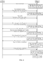
FIG. 2 is a timing chart of a firmware upgrade in accordance with an embodiment of the present invention; -
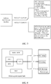
FIG. 3 is a schematic diagram of a firmware activation in accordance with an embodiment of the present invention; -
FIG. 4 is a schematic diagram of an internal online upgrade register bank in an optical module in accordance with an embodiment of the present invention; -
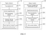
FIG. 5 is a schematic diagram of a composition structure of a firmware upgrade system in accordance with an embodiment of the present invention. - Hereinafter, in conjunction with the accompanying drawings and specific embodiments, the technical solution of the present invention will be described in detail.
- In the firmware upgrade method provided in the embodiment of the present invention, an optical module is configured with a firmware upgrade type identification register, and the firmware upgrade type identification register saves type identifications of firmwares whose upgrade is supported by the optical module, wherein the method mainly comprises: writing a type identification of a to-be-upgraded firmware into a firmware upgrade type identification register corresponding to the optical module, and judging whether the optical module supports the type of the to-be-upgraded firmware by reading the firmware upgrade state register of the optical module; when determining that the optical module supports the type of the to-be-upgraded firmware, executing a corresponding type of firmware upgrade processing on the optical module.
- The executive body of the method may be an upper computer, and the upgrade method can also be described as: the upper computer writing the type identification of the to-be-upgraded firmware into the firmware upgrade type identification register corresponding to the optical module, and by reading the firmware upgrade state register of the optical module, judging whether the optical module supports the type of the to-be-upgraded firmware or not; and executing the corresponding type of firmware upgrade processing on the optical module when determining that the type of the to-be-upgraded firmware is supported by the optical module.
- In the embodiment of the present invention, it is possible to enable a reserved register in the MDIO MSA as the firmware upgrade type identification register; preferably, the reserved register B052 in the MDIO MSA can be set as a firmware upgrade type identification register, and 15-12 bits in the register can be used as the firmware upgrade type identification, and the corresponding values of specific types are shown in table 2 below. Table 2 lists three firmware types: MCU software image, FPGA logic image, and digital signal processer (DSP) chip image, of course, the embodiment of the present invention is not limited to these firmware types, and other firmware types can be extended based on these. Furthermore, in the embodiment of the present invention, an entry of not supported firmware types is added in the upgrade command failure reason bit information of the original register B051 in the MDIO MSA, whose corresponding values are shown in Table 3.
Table 2 Hexadecimal address Size (byte) Access Type Bit Register Name/bit name Description Initial Value B052 1 Online upgrade firmware type identification Read/Write 15∼12 Firmware Type 0: MCU image 0 1: FPGA image 2: DSP chip image 3∼15: Reserved read 11∼0 Reserved 0 table 3 Module upgrade state 0000h B051h 1 read 15∼14 Upgrade command execution state 00: Idle 00b 01: The command completes successfully 10: The command is in execution 11: The command fails 13 The state of service being affected when upgrading to the downloaded image 0: Upgrading to the current downloaded image will not affect the service 0b 1: Upgrading to the current downloaded image will affect the service 12 Image Run 0: Image A 0b 1: Image B 11∼10 Image A state 00: No image 00b 01: There is a valid image 10: There is a damaged image 11: Reserved 9∼8 Image B state 00: No image 00b 01: There is a valid image 10: There is a damaged image 11: Reserved 7 Image commit 0: Image A 0b 1: Image B 6∼0 Upgrade command failure reason 0: No error 0b 1: CRC checksum error 2: Image length error 3: Flash write operation error 4: Firmware type is not supported 5-127: Reserved - Since the register B052 is non-volatile, it resumes to its last set value after the power-down or reset and the reboot.
- As a preferred embodiment of the present invention, the judging whether the optical module supports the type of the to-be-upgraded firmware by reading the firmware upgrade state register of the optical module comprises:
reading the upgrade command execution state bit in the firmware upgrade state register of the optical module, if the read bit indicates that the command is executed successfully, determining that the optical module supports the upgrade of the firmware whose type corresponds to the written firmware type identification; if the command execution fails, reading the upgrade command execution failure reason register in the firmware upgrade state register of the optical module, if the reason register indicates that the type of the firmware is not supported, determining that the optical module does not support the upgrade of the firmware whose type corresponds to the written firmware type identification. - When determining that the optical module supports the type of the to-be-upgraded firmware, the executing the corresponding type of firmware upgrade processing on the optical module comprises:
- sending a download instruction to the optical module, and transmitting image data of the to-be-upgraded firmware;
- after successfully transmitting the image data, sending a trial run new firmware command to the optical module to indicate the optical module to execute the trial run of the new firmware;
- after the optical module trial runs the new firmware successfully, it sending an image data commit command to the optical module, and committing the upgraded image data as default image data for the optical module starting the corresponding firmware.
- The embodiment of the present invention further provides a firmware upgrade method, configures a firmware upgrade type identification register in the optical module, wherein the firmware upgrade type identification register saves type identifications of the firmwares whose upgrade is supported by the optical module, and the method mainly comprises: upon receiving a download instruction from the upper computer, executing the corresponding type of firmware upgrade processing according to the type of the upgraded firmware written by the upper computer in the firmware upgrade type identification register.
- The executive body of the method is the optical module, therefore, the upgrade method is also described as: when the optical module receives a download instruction from the upper computer, executing the corresponding type of the firmware upgrade processing according to the type of the upgraded firmware written by the upper computer in the firmware upgrade type identification register.
- In the embodiment of the present invention, it is possible to enable one reserved register in the MDIO MSA as the firmware upgrade type identification register; preferably, the reserved register B052 in the MDIO MSA can be set as the firmware upgrade type identification register, and 15-12 bits in the register can be used as the firmware upgrade type identification, and the corresponding values of the specific types are shown in table 2. Since the register B052 is nonvolatile, it resumes to its last set value after the power-down or the reset and reboot.
- As a preferred embodiment of the present invention, the optical module executing the corresponding type of firmware upgrade processing comprises:
- after receiving a download instruction sent by the upper computer, receiving image data of the to-be-upgraded firmware transmitted by the upper computer, and after the image data are downloaded successfully, sending a download completed message to the upper computer;
- after receiving the trial run new firmware command sent by the upper computer, according to the firmware type identification in the command, calling a corresponding type of firmware activation strategy via a unified interface to execute the trial run of the new firmware, and after the trial run is successful, sending a firmware trial run successful message to the upper computer;
- after receiving the image data commit command sent by the upper computer, according to the commit command, setting the upgraded image data as the default image data for starting the corresponding firmware.
- In the following, in combination with the timing chart shown in
FIG. 2 , the firmware upgrade process executed between the upper computer and the optical module will be described in further detail. The firmware upgrade process mainly comprises:
in step 201, the upper computer sets the upgrade firmware type in the optical module. - Specifically, the upper computer writes the type identification of the to-be-upgraded firmware into the firmware upgrade type identification register of the optical module.
- In step 202, the upper computer queries whether the setting of the upgrade firmware type is successful or not.
- Specifically, the upper computer reads the upgrade command execution state bit in the firmware upgrade state register of the optical module, if the read bit indicates that the command is executed successfully, it determines that the optical module supports the upgrade of the firmware whose type corresponds to the written firmware type identification; if the command is executed unsuccessfully, it reads the upgrade command execution failure reason register in the firmware upgrade state register of the optical module, and if the reason register indicates that the type of the firmware is not supported, it determines that the optical module does not support the upgrade of the firmware whose type corresponds to the written firmware type identification. After successfully setting the type of the to-be-upgraded firmware, it proceeds to the next steps; and after the setting of the type of the to-be-upgraded firmware fails, it terminates the operation.
- In steps 203-205, the upper computer sends a download instruction to the optical module, and transmits image data of the to-be-upgraded firmware.
- One possible data transmission process is: the upper computer segmenting the image data of the to-be-upgraded firmware into a plurality of data blocks, each data block should comprise a data portion and a cyclic redundancy checks (CRC) checksum; once any error occurs during the current data block receiving process, the optical module notifies the upper computer, and the upper computer re-transmits the data block; if the same data block has several CRC errors, the upper computer forcibly terminates the upgrade process. When all the image data packets are transmitted completely, the upper computer sends a data transmission completed command to terminate the transmission process; the optical module will confirm that the entire image has been successfully downloaded by sending an online download completed message. Errors in the download process are recorded and fed back by the state register of the optical module.
- In step 206, after the image data is transferred successful, the upper computer transmits a trial run new firmware command to the optical module to indicate the optical module to execute the trial run of new firmware.
- In step 207, after receiving the trial run new firmware command sent by the upper computer, the optical module calls the corresponding type of firmware activation strategy via a unified interface to execute the trial run of the new firmware according to the firmware type identification in the command, and after the trial run is successful, it sends a firmware trial run successful message to the upper computer.
- Since the activation methods of different image data will be different, the embodiment of the present invention uses the unified dynamic interface to call the corresponding type of firmware activation strategy to execute the trial run of the new firmware through the optical module using the firmware type identification in the command. Take the activation of the MCU image and the FPGA image for example, as shown in
FIG. 3 , when executing the trial run of the MCU image data, the optical module calls the unified firmware activation interface to execute the corresponding MCU firmware activation step, comprising: setting the MCU firmware run flag; the MCU software reboot; boot, or management process to initiate the new MCU firmware according to the flag. When executing the trial run of the FPGA image data, the optical module calls the unified activation firmware interface to execute the corresponding FPGA firmware activation steps, comprising: saving the current FPGA important data; loading the new FPGA firmware; replying the FPGA with the pre-activated state according to the important data. - In step 208, after the optical module successfully execute a trial run of the new firmware, the upper computer sends an image data commit command to the optical module, and commits the upgraded image data as the default image data for the optical module starting the corresponding firmware.
- In step 209, after receiving the image data commit command sent by the upper computer, the optical module sets the upgraded image data as the default image data for starting the corresponding firmware according to the commit command.
- Again, as shown in
FIG. 4, FIG. 4 is a schematic diagram of an internal online upgrade register bank in the optical module. In theFIG. 4 , the online upgrade register bank comprises: upgrade control register B051, state register B04D, data transmission control register B04C, data block storage register bank (BC00∼BFFF), and firmware upgrade type identification register B052. Wherein, the upgrade control register B051 is responsible for controlling the firmware online upgrade process of the optical module; the state register B04D is responsible for the state storage in the firmware online upgrade process; the data transmission control register B04C is responsible for data exchange with the upper computer; the data block storage register bank BC00 ∼ BFFF is responsible for data storage in the online upgrade process; the firmware upgrade type identification register B052 is responsible for saving the type identification of the firmware whose upgrade is supported by the optical module, for example:identification 0 inFIG. 4 represents the MCU image type,identification 1 represents the FPGA image type andidentification 2 represents the DSP chip image type. The upper computer can execute the read/write operation on the firmware upgrade type identification register B052 of the optical module, and the write operation on the data block storage register bank, and so on. - Corresponding to the abovementioned firmware upgrade method, the embodiment of the present invention further provides a firmware upgrade system, as shown in
FIG. 5 , the system comprises: theupper computer 10 andoptical module 20;
wherein, theoptical module 20 is configured with a firmware upgrade type identification register, and the firmware upgrade type identification register saves type identifications of firmwares whose upgrade is supported by the optical module;
theupper computer 10 is configured to write the type identification of the to-be-upgraded firmware into the firmware upgrade type identification register corresponding to theoptical module 20, and judge whether theoptical module 20 supports the type of the to-be-upgraded firmware by reading the firmware upgrade state register of theoptical module 20; when determining that theoptical module 20 supports the type of the to-be-upgraded firmware, execute the corresponding type of firmware upgrade processing on theoptical module 20;
theoptical module 20 is configured to, when receiving a download instruction from theupper computer 10, execute the corresponding type of firmware upgrade processing according to the type of the upgraded firmware written by theupper computer 10 into the firmware upgrade type identification register. - Preferably, the
upper computer 10 comprises: - a
type judging unit 11, configured to write a type identification of the to-be-upgraded firmware into a firmware upgrade type identification register corresponding to theoptical module 20, and judge whether theoptical module 20 supports the type of the to-be-upgraded firmware by reading the firmware upgrade state register of theoptical module 20; - the
firmware upgrading unit 12 is configured to execute the corresponding type of firmware upgrade processing on theoptical module 20 when the judgment result of thetype judging unit 11 represents that theoptical module 20 supports the type of the to-be-upgraded firmware. - Preferably, the
type judging unit 11 is configured to read the upgrade command execution state bit in the firmware upgrade state register of theoptical module 20, if the read bit indication command is executed successfully, determine that theoptical module 20 supports the upgrade of the firmware whose type corresponds to the written firmware type identification; if the command execution fails, read the upgrade command execution failure reason register in the firmware upgrade state register of theoptical module 20, and if the reason register indicates that the firmware type is not supported, determine that theoptical module 20 does not support the upgrade of the firmware whose type corresponds to the written firmware type identification. Preferably, thefirmware upgrading unit 12 comprises: - a
data transmitting subunit 121, configured to send a download instruction to theoptical module 20, and transmit image data of the to-be-upgraded firmware; - a firmware trial-
run indicating subunit 122, configured to send a trial run new firmware command to the optical module after the image data are transmitted successfully, and indicate theoptical module 20 to execute the trial run of the new firmware; -
data indicating subunit 123, configured to, after the optical module successfully execute a trial run of the new firmware, send an image data commit command to theoptical module 20, and commit the upgraded image data as default image data for theoptical module 20 starting the corresponding firmware. - Preferably, the
optical module 20 further comprises: anupgrade processing unit 21, configured to, when receiving a download instruction from theupper computer 10, execute the corresponding type of firmware upgrade processing according to the type of the upgraded firmware written by theupper computer 10 into the firmware upgrade type identification register. - Preferably, the
upgrade processing unit 21 comprises: - a
data downloading subunit 211, configured to, after receiving the download instruction sent by theupper computer 10, receive image data of the to-be-upgraded firmware transmitted by theupper computer 10, and send a download completed message to theupper computer 10 after the image data are downloaded successfully; - a firmware
trial run sub-unit 212, configured to, after receiving a trial run new firmware command sent by theupper computer 10, execute the trial run of the new firmware by calling the corresponding type of firmware activation strategy via a unified interface according to the firmware type identification in the command, and after the trial run is successful, send a firmware trial run successful message to theupper computer 10; - a data commit
subunit 213, configured to, after receiving the image data commit command sent by theupper computer 10, set the upgraded image data as default image data for starting the corresponding firmware according to the commit command. - The
type judging unit 11, thefirmware upgrading unit 12, and thedata transmitting subunit 121, the firmware trialrun indicating subunit 122 and thedata indicating subunit 123 can be implemented by the Central Processing Unit (CPU), a Micro Processing Unit (MPU), a digital signal processor (DSP) or a Field-programmable Gate array (FPGA) of the upper computer;
theupgrade processing unit 21, as well as thedata downloading subunit 211, the firmwaretrial run subunit 212 and the data commitsubunit 213 may be implemented by the CPU, the MPU, the DSP or the FPGA of the optical module. - The embodiment of the present invention further provides a computer-readable storage medium, and the storage medium comprises a group of computer-executable instructions, and the instructions are used to execute the firmware upgrade method at the upper computer side.
- The embodiment of the present invention further provides a computer-readable storage medium, and the storage medium comprises a group of computer-executable instructions, and the instructions are used to execute the firmware upgrade method at the optical module side.
- In summary, the embodiment of the present invent uses one reserved register in the MDIO MSA as a upgrade firmware state register to reflect the current online upgrade firmware types supported by the optical module and control the online upgrade firmware types; it multiplexes the online upgrade control and state register in the MDIO MSA, and adds online upgrade command execution failure reason information in the existing online upgrade state register to unify the state indication and control method in different firmware type upgrade processes; it adds a firmware type judgment in the upgrade control timing, and performs different treatments depending on different types of the upgraded firmware, to improve the firmware upgrade control timing, achieve the universality of the control process, the scalability of the firmware type and the reusability of the register, which is conducive to the extendibility when adding firmware types in the future, extending the scope of the MDIO MSA. Adding the online firmware upgrade type identification register saves the resources of reserved registers in the MDIO MSA, greatly ensuring the scalability; the reusability of the online upgrade control timing is improved, and the implementation complexity is reduced.
- The above description is only the preferred embodiments of the present invention, and is not intended to limit the protection scope of the present invention.
Claims (12)
- A firmware upgrade method, applied in Management Data Input/Output, MDIO, Multi Source Agreement, MSA, an optical module configured with a firmware upgrade type identification register, and the firmware upgrade type identification register saving type identifications of firmwares whose upgrade is supported by the optical module, wherein the method comprises:writing a type identification of a to-be-upgraded firmware into a firmware upgrade type identification register corresponding to the optical module, characterized in that, a type of the to-be-upgraded firmware represented by the type identification comprises: a Micro Control Unit, MCU, software image type, a Field Programmable Gate Array, FPGA, logic image type and a digital signal processer, DSP, chip image type; and judging whether the optical module supports the type of the to-be-upgraded firmware by reading a firmware upgrade state register of the optical module; when determining that the optical module supports the type of the to-be-upgraded firmware, executing a corresponding type of firmware upgrade processing on the optical module;the judging whether the optical module supports the type of the to-be-upgraded firmware by reading the firmware upgrade state register of the optical module comprises:
reading an upgrade command execution state bit in the firmware upgrade state register of the optical module, if the read bit indicates that a command is executed successfully, determining that the optical module supports the upgrade of a firmware whose type corresponds to a written firmware type identification; if the execution of the command fails, reading an upgrade command execution failure reason register in the firmware upgrade state register of the optical module, if the reason register indicates that the type of the firmware is not supported, determining that the optical module does not support the upgrade of the firmware whose type corresponds to the written firmware type identification (S201, 202, 203). - The firmware upgrade method of claim 1, wherein, the executing the corresponding type of firmware upgrade processing on the optical module comprises:sending a download instruction to the optical module, and transferring image data of the to-be-upgraded firmware;after the image data is transferred successfully, sending a trial run new firmware command to the optical module, and indicating the optical module to execute a trial run of a new firmware;after the optical module executes a trial run of the new firmware successfully, sending an image data commit command to the optical module, and committing the upgraded image data as default image data for the optical module starting a corresponding firmware (S204).
- The firmware upgrade method according to claim 2, upon receiving the download instruction from an upper computer, according to the type of upgraded firmware written by the upper computer into the firmware upgrade type identification register, executing a corresponding type of firmware upgrade processing (S205).
- The firmware upgrade method of claim 3, wherein the executing the corresponding type of firmware upgrade processing comprises:after receiving the download instruction sent by the upper computer, receiving the image data of to-be-upgraded firmware transferred by the upper computer, and after the image data are downloaded successfully, sending a download completed message to the upper computer;upon receiving a trial run new firmware command sent by the upper computer, according to a firmware type identification in the command, calling a corresponding type of firmware activation strategy via a unified interface to execute a trial run of the new firmware, and after the trial run is successful, sending a firmware trial run successful message to the upper computer;after receiving an image data commit command sent by the upper computer, setting the upgraded image data as default image data for starting a corresponding firmware according to the commit command.
- The firmware upgrade method of claim 3 or 4, wherein, the firmware upgrade type identification register is a reserved register of management data input/output MultiSource Agreement (MDIO MSA).
- An upper computer (10), applied in Management Data Input/Output, MDIO, Multi Source Agreement, MSA, an optical module (20) configured with a firmware upgrade type identification register, the firmware upgrade type identification register saving type identifications of firmwares whose upgrade is supported by the optical module, wherein the upper computer comprises:a type judging unit (11), configured to write a type identification of a to-be-upgraded firmware into a firmware upgrade type identification register corresponding to the optical module, characterized in that, a type of the to-be-upgraded firmware represented by the type identification comprises: a Micro Control Unit, MCU, software image type, a Field Programmable Gate Array, FPGA, logic image type and a digital signal processer, DSP, chip image type; and judging whether the optical module supports the type of the to-be-upgraded firmware by reading a firmware upgrade state register of the optical module;a firmware upgrading unit (12), configured to execute a corresponding type of firmware upgrade processing on the optical module (20)when a judgment result of the type judging unit represents that the optical module supports the type of the to-be-upgraded firmware;characterized in that, the type judging unit (11) is further configured to read an upgrade command execution state bit in the firmware upgrade state register of the optical module (20), if the read bit indicates that a command is executed successfully, determine that the optical module supports the upgrade of a firmware whose type corresponds to a written firmware type identification; if the execution of the command fails, read an upgrade command execution failure reason register in the firmware upgrade state register of the optical module (20), and if the reason register indicates that a firmware type is not supported, determine that the optical module (20) does not support the upgrade of the firmware whose type corresponds to the written firmware type identification.
- The upper computer of claim 6, wherein, the firmware upgrading unit (12) comprises:a data transmitting subunit(121), configured to send a download instruction to the optical module (20), and transfer image data of the to-be-upgraded firmware;a firmware trial-run indicating subunit (122), configured to send a trial run new firmware command to the optical module (20) after the image data is transferred successfully, and indicate the optical module (20) to execute a trial run of a new firmware;a data indicating subunit (123), configured to, after the optical module (20) executes a trial run of the new firmware successfully, send an image data commit command to the optical module (20), and commit the upgraded image data as default image data for the optical module(20) starting a corresponding firmware.
- The upper computer of claim 6 or 7, wherein the optical module (20) is configured with a firmware upgrade type identification register, and the firmware upgrade type identification register saves type identifications of firmwares whose upgrade is supported by the optical module (20), and the optical module (20) further comprises:
an upgrade processing unit (21), configured to, when receiving the download instruction from the upper computer (10), according to the type of upgraded firmware written by the upper computer in the firmware upgrade type identification register, execute a corresponding type of firmware upgrade processing. - The upper computer of claim 8, wherein, the upgrade processing unit (21) comprises:a data downloading subunit (211), configured to, after receiving the download instruction sent by the upper computer (10), receive image data of a to-be-upgraded firmware transmitted by the upper computer, and after the image data are downloaded successfully, send a download completed message to the upper computer (10);a firmware trial run subunit (212), configured to, after receiving the trial run new firmware command sent by the upper computer (10), call a corresponding type of firmware activation strategy via a unified interface to execute a trial run of the new firmware according to a firmware type identification in the command, and after the trial run is successful, send a firmware trial run successful message to the upper computer (10);a data commit subunit (213), configured to, after receiving the image data commit command sent by the upper computer (10), set the upgraded image data as default image data for starting a corresponding firmware according to the commit command.
- The upper computer of claim 8 or 9, wherein, the firmware upgrade type identification register is a reserved register of management data input/output Multi-Source Agreement (MDIO MSA).
- A firmware upgrade system, wherein the system comprises the upper computer (10) of any one of claims 6-10; the optical module (20) is configured with a firmware upgrade type identification register, and the firmware upgrade type identification register saves type identifications of firmwares whose upgrade is supported by the optical module (20);
the optical module (20) is configured to, when receiving a download instruction from the upper computer, execute a corresponding type of firmware upgrade processing according to the type of an upgraded firmware written by the upper computer (10) into the firmware upgrade type identification register. - A computer-readable storage medium, wherein the storage medium comprises a group of computer-executable instructions, and the instructions are used to execute the firmware upgrade method of any one of claims 1-5.
Applications Claiming Priority (2)
| Application Number | Priority Date | Filing Date | Title |
|---|---|---|---|
| CN201310469841.2A CN104579719B (en) | 2013-10-10 | 2013-10-10 | A kind of upgrade method and system, host computer and optical module of firmware |
| PCT/CN2014/080222 WO2015051647A1 (en) | 2013-10-10 | 2014-06-18 | Firmware upgrade method and system, upper computer and optical module |
Publications (3)
| Publication Number | Publication Date |
|---|---|
| EP3043512A1 EP3043512A1 (en) | 2016-07-13 |
| EP3043512A4 EP3043512A4 (en) | 2017-01-04 |
| EP3043512B1 true EP3043512B1 (en) | 2020-01-01 |
Family
ID=52812500
Family Applications (1)
| Application Number | Title | Priority Date | Filing Date |
|---|---|---|---|
| EP14852023.2A Active EP3043512B1 (en) | 2013-10-10 | 2014-06-18 | Firmware upgrade method and system, upper computer and optical module |
Country Status (3)
| Country | Link |
|---|---|
| EP (1) | EP3043512B1 (en) |
| CN (1) | CN104579719B (en) |
| WO (1) | WO2015051647A1 (en) |
Families Citing this family (36)
| Publication number | Priority date | Publication date | Assignee | Title |
|---|---|---|---|---|
| CN106528186A (en) * | 2015-09-09 | 2017-03-22 | 阿里巴巴集团控股有限公司 | Update method and device of resource file |
| CN106598632B (en) * | 2015-10-15 | 2022-02-18 | 中兴通讯股份有限公司 | Firmware upgrading method and device for optical module |
| CN105847067A (en) * | 2016-05-25 | 2016-08-10 | 北京小米移动软件有限公司 | Method and device for upgrading Zigbee equipment |
| CN106843932B (en) * | 2016-12-26 | 2020-07-24 | 歌尔科技有限公司 | Method and system for upgrading virtual reality device firmware |
| CN106681766B (en) * | 2016-12-26 | 2021-04-27 | 广东芬尼克兹节能设备有限公司 | Remote firmware upgrade control method and system |
| CN108694054A (en) * | 2017-04-10 | 2018-10-23 | 南昌欧菲生物识别技术有限公司 | The upgrade method and intelligent terminal of microprocessor firmware |
| CN107220091B (en) * | 2017-06-08 | 2020-06-26 | 成都欧飞凌通讯技术有限公司 | Upgrading and switching method for 100G CFP (circulating fluid protocol) main/standby image file |
| CN109144532B (en) * | 2017-06-13 | 2023-04-11 | 中兴通讯股份有限公司 | Upgrading method and device |
| CN109388413A (en) * | 2017-08-03 | 2019-02-26 | 中车株洲电力机车研究所有限公司 | A kind of FPGA method for updating program and system |
| CN109901866A (en) * | 2017-12-07 | 2019-06-18 | 航天科工惯性技术有限公司 | Online upgrading method and rotary steering system for multi-module system |
| CN108958765B (en) * | 2018-06-12 | 2022-12-09 | 新华三技术有限公司 | Method and device for upgrading optical module firmware |
| CN108984200A (en) * | 2018-07-17 | 2018-12-11 | 郑州云海信息技术有限公司 | A kind of timing updates the method and device of firmware |
| CN108599861B (en) * | 2018-07-27 | 2024-09-20 | 深圳市极致兴通科技有限公司 | Universal active optical module code writing device and equipment |
| CN109189434A (en) * | 2018-09-20 | 2019-01-11 | 安徽南瑞中天电力电子有限公司 | A kind of online upgrading method of electric energy meter |
| JP7281275B2 (en) * | 2018-12-20 | 2023-05-25 | Nttエレクトロニクス株式会社 | Module, information processing apparatus including same, and program data update method for updating program data of module |
| CN111367539A (en) * | 2018-12-25 | 2020-07-03 | 北京兆易创新科技股份有限公司 | eMMC online upgrading method and device |
| CN110018854B (en) * | 2019-03-26 | 2021-10-22 | 联想(北京)有限公司 | Firmware matching method, equipment and computer readable storage medium |
| CN110442356A (en) * | 2019-08-06 | 2019-11-12 | 东莞铭普光磁股份有限公司 | The upgrade method and device of DSP firmware |
| CN111045703B (en) * | 2019-11-07 | 2023-08-11 | 许继集团有限公司 | Battery management unit software upgrading method and system |
| CN111273930A (en) * | 2020-01-21 | 2020-06-12 | 深圳市雷赛软件技术有限公司 | Firmware upgrade control method, host computer and firmware upgrade system |
| CN111309359A (en) * | 2020-03-16 | 2020-06-19 | 深圳益邦物联科技有限公司 | Firmware remote control automatic upgrading method, electronic equipment and storage medium |
| CN111880817B (en) * | 2020-07-27 | 2023-04-07 | 北京环境特性研究所 | Remote programming method for photoelectric monitoring system |
| CN112181467B (en) * | 2020-10-10 | 2023-11-14 | 北京字节跳动网络技术有限公司 | Method and device for upgrading memory firmware of terminal, terminal and storage medium |
| CN112540785B (en) * | 2020-11-17 | 2025-01-10 | 中山市江波龙电子有限公司 | A firmware upgrade method for storage device, control device and storage device |
| CN112230967B (en) * | 2020-11-19 | 2024-03-29 | 成都新易盛通信技术股份有限公司 | A method for rolling back online upgrade of optical module firmware based on traditional partitioning |
| CN112783531A (en) * | 2021-01-29 | 2021-05-11 | 湖北三江航天红峰控制有限公司 | Method for upgrading DSP (digital Signal processor) program through Ethernet under FPGA (field programmable Gate array) and DSP (digital Signal processor) framework |
| CN114915345B (en) * | 2021-01-29 | 2023-12-01 | 青岛海信宽带多媒体技术有限公司 | Optical module |
| CN113821240B (en) * | 2021-09-03 | 2023-11-17 | 锐捷网络股份有限公司 | Firmware upgrade method, electronic device, storage medium and signal latch circuit |
| CN115268948B (en) * | 2022-07-20 | 2026-04-07 | 瑞芯微电子股份有限公司 | Firmware upgrade methods and systems, electronic devices and storage media |
| CN116301963A (en) * | 2023-01-09 | 2023-06-23 | 上海加糖科技有限公司 | System firmware upgrade method, device, equipment and storage medium |
| CN116339786B (en) * | 2023-03-29 | 2026-02-17 | 山东云海国创云计算装备产业创新中心有限公司 | Method, device and equipment for starting baseline firmware upgrade |
| CN116450179B (en) * | 2023-04-13 | 2026-04-07 | 浪潮电子信息产业股份有限公司 | Backplane online upgrade methods, devices, equipment and media |
| CN119718363A (en) * | 2023-09-28 | 2025-03-28 | 华为技术有限公司 | Optical module upgrading method and related device |
| CN118245092B (en) * | 2024-05-28 | 2024-08-09 | 浙江正泰中自控制工程有限公司 | Multi-module online upgrading method for safety control platform |
| CN119363729B (en) * | 2024-11-05 | 2025-10-14 | 天津津航计算技术研究所 | A DSP online upgrade system and method for error-correctable serial communication |
| CN119202858B (en) * | 2024-11-27 | 2025-04-08 | 威胜集团有限公司 | Identification method, medium and terminal of intelligent metering equipment upgrade package |
Family Cites Families (6)
| Publication number | Priority date | Publication date | Assignee | Title |
|---|---|---|---|---|
| CN1584822B (en) * | 2003-08-19 | 2010-04-21 | 联想(北京)有限公司 | Method for updating computer fixing ware program |
| GB2449193B (en) * | 2004-07-07 | 2009-03-04 | Dell Products Lp | System and method for emdedding optical drive compatibility information in optical media |
| CN102098590B (en) * | 2009-12-15 | 2014-04-30 | 中兴通讯股份有限公司 | Automatic upgrading method and system of firmware version of optical network unit |
| CN102195798B (en) * | 2010-03-16 | 2015-08-12 | 中兴通讯股份有限公司 | A kind of method and system of optical network unit of upgrading |
| CN101950253B (en) * | 2010-08-12 | 2013-03-13 | 深圳市共进电子股份有限公司 | Method for upgrading optical module firmware in optical network unit by utilizing WEB webpage interface |
| CN103248424A (en) * | 2012-02-14 | 2013-08-14 | 深圳市卓翼科技股份有限公司 | Optical module firmware upgrading method and system |
-
2013
- 2013-10-10 CN CN201310469841.2A patent/CN104579719B/en active Active
-
2014
- 2014-06-18 WO PCT/CN2014/080222 patent/WO2015051647A1/en not_active Ceased
- 2014-06-18 EP EP14852023.2A patent/EP3043512B1/en active Active
Non-Patent Citations (1)
| Title |
|---|
| None * |
Also Published As
| Publication number | Publication date |
|---|---|
| CN104579719B (en) | 2019-07-19 |
| CN104579719A (en) | 2015-04-29 |
| EP3043512A4 (en) | 2017-01-04 |
| EP3043512A1 (en) | 2016-07-13 |
| WO2015051647A1 (en) | 2015-04-16 |
Similar Documents
| Publication | Publication Date | Title |
|---|---|---|
| EP3043512A1 (en) | Firmware upgrade method and system, upper computer and optical module | |
| US10845868B2 (en) | Methods and apparatus for running and booting an inter-processor communication link between independently operable processors | |
| CN108616382B (en) | Method, device, network card and device for upgrading network card firmware | |
| CN110073333B (en) | Method and system for recovering logic in FPGA chip and FPGA device | |
| CN106598632B (en) | Firmware upgrading method and device for optical module | |
| EP4407443A1 (en) | Application upgrading method and apparatus, and computing device and chip system | |
| KR101703403B1 (en) | Remote direct memory access with reduced latency | |
| CN117648109B (en) | Differential upgrading method, system and medium based on Flash page alignment mode | |
| US9092334B2 (en) | Method for shortening enumeration of tightly coupled USB device | |
| CN116627869B (en) | Data transmission method and device applied to electronic equipment | |
| CN113886297B (en) | SPI concurrent communication SE device and method based on DMA | |
| CN110445580B (en) | Data transmission method and device, storage medium, and electronic device | |
| CN120179270A (en) | Firmware upgrade method, device, first device and computer readable storage medium | |
| CN120179272A (en) | Firmware upgrade backup method, system and storage medium based on external Flash | |
| WO2021254280A1 (en) | Disk mounting method and device, storage medium, and electronic device | |
| US12197325B2 (en) | Storage apparatus and method of controlling storage controller | |
| CN116644011B (en) | A quick identification method, device, equipment and storage medium for I2C devices | |
| CN102169439B (en) | Data transmission system | |
| CN102843707B (en) | The communication means of BBU Yu RRU and base station | |
| US11334402B2 (en) | SDIO chip-to-chip interconnect protocol extension for slow devices and power savings | |
| CN120762518B (en) | A low-power hot-start method for multi-core systems and the multi-core system | |
| CN117880364B (en) | A data transmission method, system and related device | |
| US7809993B2 (en) | Apparatus, system, and method for receiving digital instructions at devices sharing an identity | |
| CN102929749A (en) | Method and device for switching storage element and extension element on mobile terminal | |
| US20250217073A1 (en) | Storage system |
Legal Events
| Date | Code | Title | Description |
|---|---|---|---|
| PUAI | Public reference made under article 153(3) epc to a published international application that has entered the european phase |
Free format text: ORIGINAL CODE: 0009012 |
|
| 17P | Request for examination filed |
Effective date: 20160408 |
|
| AK | Designated contracting states |
Kind code of ref document: A1 Designated state(s): AL AT BE BG CH CY CZ DE DK EE ES FI FR GB GR HR HU IE IS IT LI LT LU LV MC MK MT NL NO PL PT RO RS SE SI SK SM TR |
|
| AX | Request for extension of the european patent |
Extension state: BA ME |
|
| A4 | Supplementary search report drawn up and despatched |
Effective date: 20161207 |
|
| RIC1 | Information provided on ipc code assigned before grant |
Ipc: H04L 12/24 20060101AFI20161201BHEP Ipc: G06F 9/445 20060101ALI20161201BHEP |
|
| DAX | Request for extension of the european patent (deleted) | ||
| STAA | Information on the status of an ep patent application or granted ep patent |
Free format text: STATUS: EXAMINATION IS IN PROGRESS |
|
| 17Q | First examination report despatched |
Effective date: 20170908 |
|
| RIC1 | Information provided on ipc code assigned before grant |
Ipc: G06F 8/654 20180101ALI20190614BHEP Ipc: H04L 12/24 20060101AFI20190614BHEP Ipc: G06F 9/445 20180101ALI20190614BHEP |
|
| GRAP | Despatch of communication of intention to grant a patent |
Free format text: ORIGINAL CODE: EPIDOSNIGR1 |
|
| STAA | Information on the status of an ep patent application or granted ep patent |
Free format text: STATUS: GRANT OF PATENT IS INTENDED |
|
| INTG | Intention to grant announced |
Effective date: 20190726 |
|
| GRAS | Grant fee paid |
Free format text: ORIGINAL CODE: EPIDOSNIGR3 |
|
| GRAA | (expected) grant |
Free format text: ORIGINAL CODE: 0009210 |
|
| STAA | Information on the status of an ep patent application or granted ep patent |
Free format text: STATUS: THE PATENT HAS BEEN GRANTED |
|
| AK | Designated contracting states |
Kind code of ref document: B1 Designated state(s): AL AT BE BG CH CY CZ DE DK EE ES FI FR GB GR HR HU IE IS IT LI LT LU LV MC MK MT NL NO PL PT RO RS SE SI SK SM TR |
|
| REG | Reference to a national code |
Ref country code: GB Ref legal event code: FG4D |
|
| REG | Reference to a national code |
Ref country code: CH Ref legal event code: EP Ref country code: AT Ref legal event code: REF Ref document number: 1221173 Country of ref document: AT Kind code of ref document: T Effective date: 20200115 |
|
| REG | Reference to a national code |
Ref country code: IE Ref legal event code: FG4D |
|
| REG | Reference to a national code |
Ref country code: DE Ref legal event code: R096 Ref document number: 602014059465 Country of ref document: DE |
|
| REG | Reference to a national code |
Ref country code: NL Ref legal event code: MP Effective date: 20200101 |
|
| REG | Reference to a national code |
Ref country code: LT Ref legal event code: MG4D |
|
| PG25 | Lapsed in a contracting state [announced via postgrant information from national office to epo] |
Ref country code: NO Free format text: LAPSE BECAUSE OF FAILURE TO SUBMIT A TRANSLATION OF THE DESCRIPTION OR TO PAY THE FEE WITHIN THE PRESCRIBED TIME-LIMIT Effective date: 20200401 Ref country code: FI Free format text: LAPSE BECAUSE OF FAILURE TO SUBMIT A TRANSLATION OF THE DESCRIPTION OR TO PAY THE FEE WITHIN THE PRESCRIBED TIME-LIMIT Effective date: 20200101 Ref country code: RS Free format text: LAPSE BECAUSE OF FAILURE TO SUBMIT A TRANSLATION OF THE DESCRIPTION OR TO PAY THE FEE WITHIN THE PRESCRIBED TIME-LIMIT Effective date: 20200101 Ref country code: CZ Free format text: LAPSE BECAUSE OF FAILURE TO SUBMIT A TRANSLATION OF THE DESCRIPTION OR TO PAY THE FEE WITHIN THE PRESCRIBED TIME-LIMIT Effective date: 20200101 Ref country code: NL Free format text: LAPSE BECAUSE OF FAILURE TO SUBMIT A TRANSLATION OF THE DESCRIPTION OR TO PAY THE FEE WITHIN THE PRESCRIBED TIME-LIMIT Effective date: 20200101 Ref country code: LT Free format text: LAPSE BECAUSE OF FAILURE TO SUBMIT A TRANSLATION OF THE DESCRIPTION OR TO PAY THE FEE WITHIN THE PRESCRIBED TIME-LIMIT Effective date: 20200101 Ref country code: PT Free format text: LAPSE BECAUSE OF FAILURE TO SUBMIT A TRANSLATION OF THE DESCRIPTION OR TO PAY THE FEE WITHIN THE PRESCRIBED TIME-LIMIT Effective date: 20200527 |
|
| PG25 | Lapsed in a contracting state [announced via postgrant information from national office to epo] |
Ref country code: HR Free format text: LAPSE BECAUSE OF FAILURE TO SUBMIT A TRANSLATION OF THE DESCRIPTION OR TO PAY THE FEE WITHIN THE PRESCRIBED TIME-LIMIT Effective date: 20200101 Ref country code: GR Free format text: LAPSE BECAUSE OF FAILURE TO SUBMIT A TRANSLATION OF THE DESCRIPTION OR TO PAY THE FEE WITHIN THE PRESCRIBED TIME-LIMIT Effective date: 20200402 Ref country code: LV Free format text: LAPSE BECAUSE OF FAILURE TO SUBMIT A TRANSLATION OF THE DESCRIPTION OR TO PAY THE FEE WITHIN THE PRESCRIBED TIME-LIMIT Effective date: 20200101 Ref country code: BG Free format text: LAPSE BECAUSE OF FAILURE TO SUBMIT A TRANSLATION OF THE DESCRIPTION OR TO PAY THE FEE WITHIN THE PRESCRIBED TIME-LIMIT Effective date: 20200401 Ref country code: IS Free format text: LAPSE BECAUSE OF FAILURE TO SUBMIT A TRANSLATION OF THE DESCRIPTION OR TO PAY THE FEE WITHIN THE PRESCRIBED TIME-LIMIT Effective date: 20200501 Ref country code: SE Free format text: LAPSE BECAUSE OF FAILURE TO SUBMIT A TRANSLATION OF THE DESCRIPTION OR TO PAY THE FEE WITHIN THE PRESCRIBED TIME-LIMIT Effective date: 20200101 |
|
| REG | Reference to a national code |
Ref country code: DE Ref legal event code: R097 Ref document number: 602014059465 Country of ref document: DE |
|
| PG25 | Lapsed in a contracting state [announced via postgrant information from national office to epo] |
Ref country code: ES Free format text: LAPSE BECAUSE OF FAILURE TO SUBMIT A TRANSLATION OF THE DESCRIPTION OR TO PAY THE FEE WITHIN THE PRESCRIBED TIME-LIMIT Effective date: 20200101 Ref country code: SK Free format text: LAPSE BECAUSE OF FAILURE TO SUBMIT A TRANSLATION OF THE DESCRIPTION OR TO PAY THE FEE WITHIN THE PRESCRIBED TIME-LIMIT Effective date: 20200101 Ref country code: EE Free format text: LAPSE BECAUSE OF FAILURE TO SUBMIT A TRANSLATION OF THE DESCRIPTION OR TO PAY THE FEE WITHIN THE PRESCRIBED TIME-LIMIT Effective date: 20200101 Ref country code: SM Free format text: LAPSE BECAUSE OF FAILURE TO SUBMIT A TRANSLATION OF THE DESCRIPTION OR TO PAY THE FEE WITHIN THE PRESCRIBED TIME-LIMIT Effective date: 20200101 Ref country code: DK Free format text: LAPSE BECAUSE OF FAILURE TO SUBMIT A TRANSLATION OF THE DESCRIPTION OR TO PAY THE FEE WITHIN THE PRESCRIBED TIME-LIMIT Effective date: 20200101 Ref country code: RO Free format text: LAPSE BECAUSE OF FAILURE TO SUBMIT A TRANSLATION OF THE DESCRIPTION OR TO PAY THE FEE WITHIN THE PRESCRIBED TIME-LIMIT Effective date: 20200101 |
|
| PLBE | No opposition filed within time limit |
Free format text: ORIGINAL CODE: 0009261 |
|
| STAA | Information on the status of an ep patent application or granted ep patent |
Free format text: STATUS: NO OPPOSITION FILED WITHIN TIME LIMIT |
|
| REG | Reference to a national code |
Ref country code: AT Ref legal event code: MK05 Ref document number: 1221173 Country of ref document: AT Kind code of ref document: T Effective date: 20200101 |
|
| 26N | No opposition filed |
Effective date: 20201002 |
|
| PG25 | Lapsed in a contracting state [announced via postgrant information from national office to epo] |
Ref country code: AT Free format text: LAPSE BECAUSE OF FAILURE TO SUBMIT A TRANSLATION OF THE DESCRIPTION OR TO PAY THE FEE WITHIN THE PRESCRIBED TIME-LIMIT Effective date: 20200101 Ref country code: MC Free format text: LAPSE BECAUSE OF FAILURE TO SUBMIT A TRANSLATION OF THE DESCRIPTION OR TO PAY THE FEE WITHIN THE PRESCRIBED TIME-LIMIT Effective date: 20200101 Ref country code: IT Free format text: LAPSE BECAUSE OF FAILURE TO SUBMIT A TRANSLATION OF THE DESCRIPTION OR TO PAY THE FEE WITHIN THE PRESCRIBED TIME-LIMIT Effective date: 20200101 |
|
| REG | Reference to a national code |
Ref country code: CH Ref legal event code: PL |
|
| PG25 | Lapsed in a contracting state [announced via postgrant information from national office to epo] |
Ref country code: PL Free format text: LAPSE BECAUSE OF FAILURE TO SUBMIT A TRANSLATION OF THE DESCRIPTION OR TO PAY THE FEE WITHIN THE PRESCRIBED TIME-LIMIT Effective date: 20200101 Ref country code: SI Free format text: LAPSE BECAUSE OF FAILURE TO SUBMIT A TRANSLATION OF THE DESCRIPTION OR TO PAY THE FEE WITHIN THE PRESCRIBED TIME-LIMIT Effective date: 20200101 |
|
| GBPC | Gb: european patent ceased through non-payment of renewal fee |
Effective date: 20200618 |
|
| PG25 | Lapsed in a contracting state [announced via postgrant information from national office to epo] |
Ref country code: LU Free format text: LAPSE BECAUSE OF NON-PAYMENT OF DUE FEES Effective date: 20200618 |
|
| REG | Reference to a national code |
Ref country code: BE Ref legal event code: MM Effective date: 20200630 |
|
| PG25 | Lapsed in a contracting state [announced via postgrant information from national office to epo] |
Ref country code: LI Free format text: LAPSE BECAUSE OF NON-PAYMENT OF DUE FEES Effective date: 20200630 Ref country code: CH Free format text: LAPSE BECAUSE OF NON-PAYMENT OF DUE FEES Effective date: 20200630 Ref country code: GB Free format text: LAPSE BECAUSE OF NON-PAYMENT OF DUE FEES Effective date: 20200618 Ref country code: IE Free format text: LAPSE BECAUSE OF NON-PAYMENT OF DUE FEES Effective date: 20200618 |
|
| PG25 | Lapsed in a contracting state [announced via postgrant information from national office to epo] |
Ref country code: BE Free format text: LAPSE BECAUSE OF NON-PAYMENT OF DUE FEES Effective date: 20200630 |
|
| PGFP | Annual fee paid to national office [announced via postgrant information from national office to epo] |
Ref country code: DE Payment date: 20201231 Year of fee payment: 7 |
|
| REG | Reference to a national code |
Ref country code: DE Ref legal event code: R079 Ref document number: 602014059465 Country of ref document: DE Free format text: PREVIOUS MAIN CLASS: H04L0012240000 Ipc: H04L0041000000 |
|
| REG | Reference to a national code |
Ref country code: DE Ref legal event code: R119 Ref document number: 602014059465 Country of ref document: DE |
|
| PG25 | Lapsed in a contracting state [announced via postgrant information from national office to epo] |
Ref country code: DE Free format text: LAPSE BECAUSE OF NON-PAYMENT OF DUE FEES Effective date: 20220101 |
|
| PG25 | Lapsed in a contracting state [announced via postgrant information from national office to epo] |
Ref country code: TR Free format text: LAPSE BECAUSE OF FAILURE TO SUBMIT A TRANSLATION OF THE DESCRIPTION OR TO PAY THE FEE WITHIN THE PRESCRIBED TIME-LIMIT Effective date: 20200101 Ref country code: MT Free format text: LAPSE BECAUSE OF FAILURE TO SUBMIT A TRANSLATION OF THE DESCRIPTION OR TO PAY THE FEE WITHIN THE PRESCRIBED TIME-LIMIT Effective date: 20200101 Ref country code: CY Free format text: LAPSE BECAUSE OF FAILURE TO SUBMIT A TRANSLATION OF THE DESCRIPTION OR TO PAY THE FEE WITHIN THE PRESCRIBED TIME-LIMIT Effective date: 20200101 |
|
| PG25 | Lapsed in a contracting state [announced via postgrant information from national office to epo] |
Ref country code: MK Free format text: LAPSE BECAUSE OF FAILURE TO SUBMIT A TRANSLATION OF THE DESCRIPTION OR TO PAY THE FEE WITHIN THE PRESCRIBED TIME-LIMIT Effective date: 20200101 Ref country code: AL Free format text: LAPSE BECAUSE OF FAILURE TO SUBMIT A TRANSLATION OF THE DESCRIPTION OR TO PAY THE FEE WITHIN THE PRESCRIBED TIME-LIMIT Effective date: 20200101 |
|
| REG | Reference to a national code |
Ref country code: FR Ref legal event code: PLFP Year of fee payment: 10 |
|
| PGFP | Annual fee paid to national office [announced via postgrant information from national office to epo] |
Ref country code: FR Payment date: 20250409 Year of fee payment: 12 |