EP3043423B1 - Electric device system - Google Patents
Electric device system Download PDFInfo
- Publication number
- EP3043423B1 EP3043423B1 EP15196259.4A EP15196259A EP3043423B1 EP 3043423 B1 EP3043423 B1 EP 3043423B1 EP 15196259 A EP15196259 A EP 15196259A EP 3043423 B1 EP3043423 B1 EP 3043423B1
- Authority
- EP
- European Patent Office
- Prior art keywords
- unit
- connecting terminal
- recess
- electric device
- bulging
- Prior art date
- Legal status (The legal status is an assumption and is not a legal conclusion. Google has not performed a legal analysis and makes no representation as to the accuracy of the status listed.)
- Not-in-force
Links
Images







Classifications
-
- H—ELECTRICITY
- H05—ELECTRIC TECHNIQUES NOT OTHERWISE PROVIDED FOR
- H05K—PRINTED CIRCUITS; CASINGS OR CONSTRUCTIONAL DETAILS OF ELECTRIC APPARATUS; MANUFACTURE OF ASSEMBLAGES OF ELECTRICAL COMPONENTS
- H05K7/00—Constructional details common to different types of electric apparatus
- H05K7/14—Mounting supporting structure in casing or on frame or rack
- H05K7/1462—Mounting supporting structure in casing or on frame or rack for programmable logic controllers [PLC] for automation or industrial process control
- H05K7/1474—Mounting of modules, e.g. on a base or rail or wall
-
- H—ELECTRICITY
- H01—ELECTRIC ELEMENTS
- H01R—ELECTRICALLY-CONDUCTIVE CONNECTIONS; STRUCTURAL ASSOCIATIONS OF A PLURALITY OF MUTUALLY-INSULATED ELECTRICAL CONNECTING ELEMENTS; COUPLING DEVICES; CURRENT COLLECTORS
- H01R13/00—Details of coupling devices of the kinds covered by groups H01R12/70 or H01R24/00 - H01R33/00
- H01R13/02—Contact members
- H01R13/22—Contacts for co-operating by abutting
- H01R13/24—Contacts for co-operating by abutting resilient; resiliently-mounted
- H01R13/2464—Contacts for co-operating by abutting resilient; resiliently-mounted characterized by the contact point
- H01R13/2492—Contacts for co-operating by abutting resilient; resiliently-mounted characterized by the contact point multiple contact points
-
- H—ELECTRICITY
- H01—ELECTRIC ELEMENTS
- H01R—ELECTRICALLY-CONDUCTIVE CONNECTIONS; STRUCTURAL ASSOCIATIONS OF A PLURALITY OF MUTUALLY-INSULATED ELECTRICAL CONNECTING ELEMENTS; COUPLING DEVICES; CURRENT COLLECTORS
- H01R13/00—Details of coupling devices of the kinds covered by groups H01R12/70 or H01R24/00 - H01R33/00
- H01R13/46—Bases; Cases
- H01R13/514—Bases; Cases composed as a modular blocks or assembly, i.e. composed of co-operating parts provided with contact members or holding contact members between them
-
- H—ELECTRICITY
- H01—ELECTRIC ELEMENTS
- H01R—ELECTRICALLY-CONDUCTIVE CONNECTIONS; STRUCTURAL ASSOCIATIONS OF A PLURALITY OF MUTUALLY-INSULATED ELECTRICAL CONNECTING ELEMENTS; COUPLING DEVICES; CURRENT COLLECTORS
- H01R13/00—Details of coupling devices of the kinds covered by groups H01R12/70 or H01R24/00 - H01R33/00
- H01R13/62—Means for facilitating engagement or disengagement of coupling parts or for holding them in engagement
- H01R13/629—Additional means for facilitating engagement or disengagement of coupling parts, e.g. aligning or guiding means, levers, gas pressure electrical locking indicators, manufacturing tolerances
-
- H—ELECTRICITY
- H05—ELECTRIC TECHNIQUES NOT OTHERWISE PROVIDED FOR
- H05K—PRINTED CIRCUITS; CASINGS OR CONSTRUCTIONAL DETAILS OF ELECTRIC APPARATUS; MANUFACTURE OF ASSEMBLAGES OF ELECTRICAL COMPONENTS
- H05K7/00—Constructional details common to different types of electric apparatus
- H05K7/14—Mounting supporting structure in casing or on frame or rack
- H05K7/1462—Mounting supporting structure in casing or on frame or rack for programmable logic controllers [PLC] for automation or industrial process control
- H05K7/1465—Modular PLC assemblies with separable functional units
-
- H—ELECTRICITY
- H05—ELECTRIC TECHNIQUES NOT OTHERWISE PROVIDED FOR
- H05K—PRINTED CIRCUITS; CASINGS OR CONSTRUCTIONAL DETAILS OF ELECTRIC APPARATUS; MANUFACTURE OF ASSEMBLAGES OF ELECTRICAL COMPONENTS
- H05K7/00—Constructional details common to different types of electric apparatus
- H05K7/14—Mounting supporting structure in casing or on frame or rack
- H05K7/1462—Mounting supporting structure in casing or on frame or rack for programmable logic controllers [PLC] for automation or industrial process control
- H05K7/1467—PLC mounted in a cabinet or chassis
-
- H—ELECTRICITY
- H01—ELECTRIC ELEMENTS
- H01R—ELECTRICALLY-CONDUCTIVE CONNECTIONS; STRUCTURAL ASSOCIATIONS OF A PLURALITY OF MUTUALLY-INSULATED ELECTRICAL CONNECTING ELEMENTS; COUPLING DEVICES; CURRENT COLLECTORS
- H01R13/00—Details of coupling devices of the kinds covered by groups H01R12/70 or H01R24/00 - H01R33/00
- H01R13/02—Contact members
- H01R13/22—Contacts for co-operating by abutting
- H01R13/24—Contacts for co-operating by abutting resilient; resiliently-mounted
- H01R13/2442—Contacts for co-operating by abutting resilient; resiliently-mounted with a single cantilevered beam
-
- H—ELECTRICITY
- H01—ELECTRIC ELEMENTS
- H01R—ELECTRICALLY-CONDUCTIVE CONNECTIONS; STRUCTURAL ASSOCIATIONS OF A PLURALITY OF MUTUALLY-INSULATED ELECTRICAL CONNECTING ELEMENTS; COUPLING DEVICES; CURRENT COLLECTORS
- H01R9/00—Structural associations of a plurality of mutually-insulated electrical connecting elements, e.g. terminal strips or terminal blocks; Terminals or binding posts mounted upon a base or in a case; Bases therefor
- H01R9/22—Bases, e.g. strip, block, panel
- H01R9/24—Terminal blocks
- H01R9/26—Clip-on terminal blocks for side-by-side rail- or strip-mounting
- H01R9/2675—Electrical interconnections between two blocks, e.g. by means of busbars
Definitions
- the present invention relates to an electric device system including a plurality of electric device units.
- a remote terminal device (hereinafter, also simply referred to as a remote terminal device) of a Programmable Logic Controller (PLC) can be cited as a typical example of the electric device system having the configuration.
- PLC Programmable Logic Controller
- the remote terminal device includes a communication unit and one or more I/O unit that can conduct communication with the communication unit through a serial bus line and a unidirectional communication line, and the communication unit and the I/O unit are generally formed into a building block type such that the I/O units are provided in the communication unit while continuously connected to each other.
- JP 6-6051 A , JP2001-217016 A , and JP 2012-182412 A disclose the remote terminal device having the configuration.
- each of the communication unit and I/O unit which are of the electric device unit, is attached to an attaching rail such as a DIN (German industry standard) rail, and the adjacent electric device units are assembled so as to be engaged with each other.
- an attaching rail such as a DIN (German industry standard) rail
- a guide groove and a projecting streak that are of a guiding mechanism are provided in a pair of electric device units adjacent to each other, and the projecting streak provided in one of the pair of electric device units is slidably guided by the guide groove provided in the other, whereby the pair of electric device units are detachably engaged with each other.
- JP2001-217016 A and JP 2012-182412 A disclose the electric device unit in which the guiding mechanism is provided.
- WO 97/10692 A1 describes an electronic module for mounting on a U-profiled support and stackable against other similar modules. The electronic modules are electrically connected together by terminals.
- EP 1 798 822 A1 describes a connector assembly which comprises a header and a socket.
- the header has a header contact member with a first contact piece and a second contact piece
- the socket has a socket contact member with a first contact piece and a second contact piece.
- the first contact piece of the socket contact member has a first protrusion and the first contact piece of the header contact member has a second protrusion, and the first protrusion and the second protrusion constitute a lock mechanism when the header is inserted into the socket.
- the second contact piece of the header contact member has a concave portion in a surface for making contact with the second contact piece.
- a gap is formed between the second contact piece and an inner surface of the concave portion.
- US 2006/0205290 A1 describes a connection contact of an electric connector. A groove is formed on a connecting section surface of an electrically conductive terminal, this groove is subjected to a bending deformation into a convex shape toward the surface side from the backside of a connecting section to form a bent convex section on the surface of the connecting terminal, and edge sections formed on both sides of this groove are positioned on the surface of the bent convex section.
- JP 2007 080843 A describes a connector.
- an inclined surface inside and a recessed part with a cross section of V shape are mounted on a surface of the contact part where the contact projecting part slides on and contacts with the contact part.
- a middle part in a width direction of the contact projecting part is formed in a measurement shape where it ingresses inside the recessed part, slides on and contacts with each inclined surface.
- the contact with the electrical connector comprises a contact section in a flat plate shape extended so that it comes into contact with the pressure contact of other electrical connectors, and a connection section that is provided at the opposite side of the contact section while an electric wire led from the outside is connected for contacting.
- a contact groove is provided on a surface in contact with the pressurizing contact section of other electric connectors at one side of the contact section.
- US 2013/0045617 A1 describes a method for manufacturing a metal component including the steps of forming a resist film on a surface of an electrode plate, making the resist film exposed to light by use of a photomask having a mask pattern, in at least part of a rim of which a fine concavity and convexity are drawn, developing the resist film, to form an opening for molding in the resist film, and epositing an electroforming material by electroforming inside the opening for molding, to mold the material.
- JP 2001 043920 A describes a contact structure of a spherical bump in which first and second contact pieces on the sides facing a spherical bump are forced into pressure contact with the spherical bump, the first contact piece has first and second protuberances forced into pressure contact with one side of the bump on both sides of a longitudinal line passing through one end of the diameter line of the spherical bump and disposed apart from each other, and the second contact piece has third and fourth protuberances forced into pressure contact with the other side of the bump on both sides of a longitudinal line passing through the other end of the diameter line of the spherical bump and disposed apart from each other.
- JP 2009 193733 A describes a fitting feeling which is obtained by relatively moving a protrusion-like sliding part installed at a conductive contact of the connector means on one side, and a groove-like sliding part installed at the conductive contact of the connector means on the other side so that they contact and go over at the time of fitting of both connector means.
- US 2014/0099803 A1 describes an electrical contact assembly including a first electrical contact having a first mating element, and a second electrical contact having a second mating element.
- the first and second electrical contacts being configured to mate together at the first and second mating elements such that the first and second mating elements engage each other at a contact interface.
- a distribution of contact pressure across the contact interface at least partially coincides with a distribution of electrical current flow across the contact interface.
- a first connecting terminal and a second connecting terminal are provided at positions corresponding to outer surfaces of the pair of electric device units adjacent to each other in order to establish the electric connection. Therefore, the first and second connecting terminals are in contact with each other while one of the pair of electric device units is assembled in the other, thereby establishing the electric connection between the electric device units.
- At least one of the first and second connecting terminals be provided so as to project from the outer surface of the electric device unit in a non-assembly state, and that at least one of the first and second connecting terminals be configured in an elastically deformable manner in a direction orthogonal to the outer surface.
- the foreign substance is located near a contact point of the first and second connecting terminals even if the foreign substance does not penetrate between the first and second connecting terminals after one of the pair of electric device units is assembled in the other, when impact is applied to the electric device unit from the outside, the foreign substance penetrates between the first and second connecting terminals due to variation of a relative position between the first and second connecting terminals, which causes the electric conduction to be blocked between the first and second connecting terminals to generate the communication error.
- An object of the present invention is to provide an electric device system that can prevent blocking of the electric connection between the electric device units.
- An electric device system includes a plurality of electric device units, which are electrically connected to each other by assembling the electric device units in line along a first direction.
- the plurality of electric device units include a first unit and a second unit, which are adjacent to each other in an assembly state, and each of the first unit and the second unit includes an insulating casing as an outer shell.
- a first connecting terminal is provided at a predetermined position in a first outer surface that is a casing surface of the first unit, the casing surface of the first unit facing the second unit in the assembly state, at least a part of the first connecting terminal projecting from the first outer surface in a non-assembly state, the first connecting terminal being elastically deformable in the first direction, and a second connecting terminal is provided at a position in a second outer surface that is a casing surface of the second unit, the casing surface of the second unit facing the first unit in the assembly state, the position in the second outer surface facing the first connecting terminal in the assembly state.
- a guiding mechanism is provided in the first unit and the second unit, the guiding mechanism slidably guiding the first unit into the second unit along a second direction orthogonal to the first direction to enable the first unit to be assembled in and removed from the second unit, and the guiding mechanism guides the first unit into the second unit in assembling the first unit in the second unit such that the first connecting terminal comes into contact with the second connecting terminal after sliding on the second outer surface.
- a bulging surface bulging out toward the second unit is provided on an exposed surface of the first connecting terminal located on the second unit side in the assembly state, and a recess is provided on an exposed surface of the second connecting terminal located on the first unit side in the assembly state.
- a part of the bulging surface is fitted in the recess in the assembly state, and therefore at least the part of the bulging surface comes into press-contact with at least a part of an opening edge of the recess to establish electric conduction between the first connecting terminal and the second connecting terminal.
- the bulging surface bulges out such that a bulging amount toward the second unit varies in a third direction orthogonal to the first direction and the second direction, and the recess includes a pair of opening edges facing each other in the third direction.
- the first connecting terminal and the second connecting terminal come into press-contact with each other at two points corresponding to the pair of opening edges of the recess in the assembly state.
- the recess may include a groove extending along the second direction.
- the bulging surface may bulge out such that a bulging amount toward the second unit varies in the second direction
- the recess may include a pair of opening edges facing each other in the second direction.
- the first connecting terminal and the second connecting terminal come into press-contact with each other at two points corresponding to the pair of opening edges of the recess in the assembly state.
- the recess may include a groove extending along a third direction orthogonal to both the first direction and the second direction.
- the bulging surface may bulge out such that a bulging amount toward the second unit varies in a third direction orthogonal to the first direction and the second direction while the bulging surface bulges out such that a bulging amount toward the second unit varies in the second direction
- the recess may include a pair of opening edges facing each other in the second direction and a pair of opening edges facing each other in the third direction.
- the first connecting terminal and the second connecting terminal come into press-contact with each other at four points corresponding to the four opening edges of the recess in the assembly state.
- the recess may include a recessed portion including an opening edge having a cyclic shape in a plan view.
- the bulging surface has a shape corresponding to the opening edge, and the first connecting terminal and the second connecting terminal are in press-contact with each other in a whole circumference of the opening edge in the assembly state.
- the first unit and the second unit may be assembled by attaching the first unit and the second unit to an attaching rail extending along the first direction.
- an attaching rail extending along the first direction.
- a direction in which the first unit and the second unit are attached to the attaching rail is aligned with the second direction.
- the plurality of electric device units may further include one or more electric device units in addition to the first unit and the second unit.
- all pairs of electric device units located adjacent to each other in the plurality of electric device units have an electric connecting structure identical to electric connecting structures of the first unit and the second unit.
- the present invention can provide the electric device system that can prevent the blocking of electric connection between electric device units.
- a remote terminal device of a PLC is illustrated as an example of an electric device system to which the present invention is applied.
- the identical or common component is designated by the identical numeral in the drawings, and the overlapping description is omitted.
- Fig. 1 is a perspective view illustrating an assembly state of a remote terminal device according to a first embodiment of the present invention. A configuration of a remote terminal device 1 of the first embodiment will be described below with reference to Fig. 1 .
- the remote terminal device 1 includes a communication unit 2A, a plurality of I/O units 2B, and an end cover 3.
- the communication unit 2A, the plurality of I/O units 2B, and the end cover 3 are assembled so as to be arrayed along an X-axis direction of a first direction.
- the communication unit 2A and the plurality of I/O units 2B correspond to a plurality of electric device units 2 constituting the remote terminal device 1 that is of the electric device system.
- the plurality of I/O units 2B have an identical shape and an identical configuration.
- the communication unit 2A is disposed on a leftmost side when the remote terminal device 1 is viewed from a front surface side (viewed along a Y-axis direction of a second direction), and the end cover 3 is disposed on a rightmost side when the remote terminal device 1 is viewed from the front surface side.
- the plurality of I/O units 2B are disposed between the communication unit 2A and end cover 3, which are disposed at both ends of the I/O units 2B, so as to be continuously connected to each other.
- the communication unit 2A is connected to a plurality of I/O units 2B through a serial bus line and a unidirectional communication line, and exchanges control data with each of the plurality of I/O units 2B.
- the communication unit 2A is connected to an externally-installed PLC (not illustrated) through a cable (not illustrated), and exchanges the control data with the PLC.
- the communication unit 2A is also equipped with a power supply circuit and a CPU that controls an IN device and an OUT device.
- each of the plurality of I/O units 2B is connected to the communication unit 2A through the serial bus line and the unidirectional communication line, and exchanges the control data with the communication unit 2A.
- Each of the plurality of I/O units is connected to a sensor and a switch (not illustrated) that are of the IN device and an actuator (not illustrated) that is of the OUT device through a cable (not illustrated), and exchanges the control data with the IN device and the OUT device.
- the end cover 3 is a decorative cover that covers an exposed right side surface of the I/O unit 2B, which is located on the rightmost side in the plurality of I/O units 2B when the remote terminal device 1 is viewed from the front surface side.
- the communication unit 2A and the plurality of I/O units 2B are attached to a DIN rail 100 of an attaching rail with a fixing member interposed therebetween.
- the adjacent units are engaged with each other while a guiding mechanism provided in each unit is interposed therebetween
- the I/O unit 2B located on the rightmost side in the plurality of I/O units 2B and the end cover 3 are also engaged with each other while the guiding mechanism provided in each unit is interposed therebetween. Therefore, the communication unit 2A, the plurality of I/O units 2B, and the end cover 3 are integrally attached to the DIN rail 100.
- each of the IN device and OUT device that are connected to the plurality of I/O units 2B conducts communication with the CPU provided in the communication unit 2A, thereby controlling a whole facility to which the remote terminal device 1 is attached. Because the remote terminal device 1 is controlled by the externally-installed PLC, the PLC can integrally control all the plurality of facilities by installing the plurality of remote terminal devices 1 in each facility.
- the plurality of I/O units 2B can be installed as many as the IN devices and OUT devices that are included in the facility to which the remote terminal device 1 is attached.
- the remote terminal device 1 includes eight I/O units 2B in total, the number of I/O units 2B can be increased and decreased based on the facility to which the remote terminal device 1 is attached.
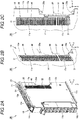
- Fig. 2A is a perspective view illustrating a front surface of the I/O unit in Fig. 1 when the I/O unit is viewed from an upper right
- Fig. 2B is an enlarged perspective view illustrating a main part of the I/O unit
- Fig. 2C is an enlarged right side view illustrating the main part of the I/O unit
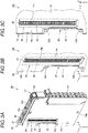
- Fig. 3A is a perspective view illustrating a front surface of the I/O unit in Fig. 1 when the I/O unit is viewed from an upper left
- Fig. 3B is an enlarged perspective view illustrating the main part of the I/O unit
- Fig. 3C is an enlarged left side view illustrating the main part of the I/O unit.
- Fig. 3A is a perspective view illustrating a front surface of the I/O unit in Fig. 1 when the I/O unit is viewed from an upper left
- Fig. 3B is an enlarged perspective view illustrating the main part of the I/O unit
- FIG. 4A is a front view of the I/O unit in Fig. 1
- Fig. 4B is a sectional view taken on a line IVB-IVB in Fig. 4A .
- the configuration of the I/O unit 2B will be described below with reference to Figs. 2 to 4 .
- the I/O unit 2B has a flat, substantially rectangular parallelepiped external form in which a width in a horizontal width is narrowed.
- a front surface 11a, a rear surface 11b, a top surface 12a, a bottom surface 12b, a right side surface 13a, and a left side surface 13b of the I/O unit 2B having the substantially rectangular parallelepiped shape are defined by an insulating casing 10 that is of an outer shell.
- a plurality of sockets are provided in the front surface 11a of the I/O unit 2B in order to connect the IN device and OUT device to the I/O unit 2B.
- An end of the cable connected to the IN device or OUT device can be inserted in each of the plurality of sockets, and the inserted end of the cable is held by the socket to provide the electric connection between the I/O unit 2B and the IN device or OUT device.
- a fixing member 20 is assembled in the rear surface 11b of the I/O unit 2B in order to attach the I/O unit 2B to the DIN rail 100.
- the fixing member 20 includes an operating knob 21, a slider 22, and an upper latching pawl 23a and a lower latching pawl 23b that are of a pair of latching pawls.
- the fixing member 20 is configured such that the upper and lower latching pawls 23a and 23b that are of a pair of latching pawls come closed to or separate from each other by vertically moving the operating knob 21. Therefore, the operating knob 21 is vertically moved while the rear surface 11b of the I/O unit 2B is applied to the DIN rail 100, which allows the I/O unit 2B to be detachably attached to the DIN rail 100.
- An upper guide groove 15a and a lower guide groove 15b which are of a pair of guide grooves, are provided in the right side surface 13a of the I/O unit 2B.
- the upper guide groove 15a is provided near an end side located on the side of the top surface 12a in the right side surface 13a of the I/O unit 2B, and extends along the Y-axis direction.
- the lower guide groove 15b is provided near an end side located on the side of the bottom surface 12b in the right side surface 13a of the I/O unit 2B, and extends along the Y-axis direction.
- the upper guide and lower guide grooves 15a and 15b that are of the pair of guide grooves are provided so as to face each other in a Z-axis direction of a third direction.
- An upper projecting streak 16a and a lower projecting streak 16b which are of a pair of projecting streaks, are provided in the left side surface 13b of the I/O unit 2B.
- the upper projecting streak 16a is provided near an end side located on the side of the top surface 12a in the left side surface 13b of the I/O unit 2B, and extends along the Y-axis direction.
- the lower projecting streak 16b is provided near the end side located on the side of the bottom surface 12b in the left side surface 13b of the I/O unit 2B, and extends along the Y-axis direction.
- the upper projecting streak 16a projects upward along the Z-axis direction
- the lower projecting streak 16b projects downward along the Z-axis direction.
- a pair of guide grooves similar to the upper and lower guide grooves 15a and 15b of the pair of guide grooves provided in the right side surface 13a of the I/O unit 2B is also provided in the right side surface of the communication unit 2A, and a pair of guide grooves similar to the upper and lower projecting streak 16a and 16b of the pair of guide grooves provided in the left side surface 13b of the I/O unit 2B is provided in the left side surface of the end cover 3.
- the upper and lower guide grooves 15a and 15b which are of the pair of guide grooves provided in the right side surface 13a of the I/O unit 2B, receive the upper and lower projecting streaks, which are of the pair of projecting streaks provided in the left side surface of the I/O unit 2B or end cover 3 that is disposed while continuously connected on the right side of the I/O unit 2B.
- the upper and lower projecting streaks 16a and 16b which are of the pair of projecting streaks provided in the left side surface 13b of the I/O unit 2B, are received by the upper and lower guide grooves, which are of the pair of guide grooves provided in the right side surface of the I/O unit 2B or communication unit 2A that is disposed while continuously connected on the left side of the I/O unit 2B.
- the pair of guide grooves and the pair of projecting streaks correspond to the guiding mechanism that engages the adjacent communication unit 2A, a plurality of I/O units 2B, and end cover 3 each two of which are located adjacent to each other.
- the pair of projecting streaks is slidably guided along the Y-axis direction by the pair of guide grooves, whereby the communication unit 2A, the plurality of I/O units 2B, and the end cover 3 can be separately inserted in and removed from the remote terminal device 1 while the engagement is performed.
- a terminal block 30 and a wiring circuit board 60 are mainly stored in the casing 10 of the I/O unit 2B.
- the terminal block 30 and the wiring circuit board 60 are held by the casing 10 while stored in the casing 10.
- the terminal block 30 includes a plurality of first connecting terminals 40 and a plurality of second connecting terminals 50 (see Figs. 2 and 3 ), and the plurality of first connecting terminals 40 and the plurality of second connecting terminals 50 are electrically connected to a plurality of conductive lines provided corresponding to the wiring circuit boards 60, respectively.
- the terminal block 30 includes a first terminal surface 31 on which the plurality of first connecting terminals 40 are exposed and a second terminal surface 32 on which the plurality of second connecting terminals 50 are exposed.
- the terminal block 30 is stored in a space of the casing 10, and the space is located on the sides of the rear surface 11b and top surface 12a of the I/O unit 2B.
- the wiring circuit board 60 mainly includes the plurality of conductive lines, is connected to the plurality of first connecting terminals 40 and the plurality of second connecting terminals 50, and is connected to the plurality of sockets provided in the front surface 11a of the I/O unit 2B.
- the wiring circuit board 60 is stored in a space of the casing 10 so as to be located in front of the terminal block 30.
- the electric conduction is established among the plurality of first connecting terminals 40 and the plurality of second connecting terminals 50, the plurality of conductive lines provided in the wiring circuit board 60, and the plurality of sockets, and the first and second connecting terminals 40 and 50, the conductive lines, and the sockets constitute the serial bus line and the unidirectional communication line.
- a first window 17a is formed at a predetermined position of the right side surface 13a of the I/O unit 2B by partially notching the casing 10, and the terminal block 30 is disposed so as to face the first window 17a.
- the first terminal surface 31 of the terminal block 30 is provided at a position corresponding to the first window 17a, and the first terminal surface 31 is exposed outward to expose the plurality of first connecting terminals 40.
- the first terminal surface 31 of the terminal block 30 extends along the Z-axis direction, and the plurality of first connecting terminals 40 are arrayed in the Z-axis direction at predetermined intervals.
- the plurality of first connecting terminals 40 are located so as to partially project outward from the right side surface 13a of the I/O unit 2B (particularly, see Figs. 2B , 4A, and 4B ).
- a second window 17b is formed at a predetermined position of the left side surface 13b of the I/O unit 2B by partially notching the casing 10, and the terminal block 30 is disposed so as to face the second window 17b.
- the second terminal surface 32 of the terminal block 30 is provided at a position corresponding to the second window 17b, and the second terminal surface 32 is exposed outward to expose the plurality of second connecting terminals 50.
- the second terminal surface 32 of the terminal block 30 extends along the Z-axis direction, and the plurality of second connecting terminals 50 are arrayed along the Z-axis direction at predetermined intervals.
- the plurality of second connecting terminals 50 are located so as to be substantially flush with the left side surface 13b of the I/O unit 2B (particularly, see Figs. 3B and 4B ).
- a terminal block having a configuration similar to the portion including the first terminal surface 31 of the terminal block 30 provided in the I/O unit 2B is also stored in the casing of the communication unit 2A, a plurality of first connecting terminals are provided in the terminal block, and the plurality of first connecting terminals are exposed on the right side surface of the communication unit 2A.
- the first and second terminal surfaces 31 and 32 of the terminal block 30 are provided at positions corresponding to the right and left side surfaces 13a and 13b, respectively, of the I/O unit 2B.
- the first terminal surface of the terminal block is provided at a position corresponding to the second terminal surface 32 provided in the left side surface 13b of the I/O unit 2B that is disposed while continuously connected to the communication unit 2A.
- the first terminal surface 31 of one of the pair of adjacent units in the communication unit 2A and a plurality of I/O units 2B and the second terminal surface 32 of the other unit are located so as to face each other, whereby the plurality of first connecting terminals 40 disposed in the first terminal surface 31 of one of the adjacent units and the plurality of second connecting terminals 50 disposed in the second terminal surface 32 of the other unit are in contact with each other, respectively.
- the pair of adjacent units are electrically connected to each other
- the remote terminal device 1 includes the communication unit 2A and a plurality of I/O units 2B that are electrically connected to one another.
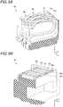
- Fig. 5A is a partially broken and perspective view illustrating the terminal block including the first connecting terminal of the I/O unit in Fig. 1
- Fig. 5B is a partially broken and perspective view illustrating the terminal block including the second connecting terminal of the I/O unit.
- the detailed configurations of the terminal block 30 and the first connecting terminal 40 and second connecting terminal 50 that are included in the terminal block 30 will be described below with reference to Fig. 5 .
- a plurality of groove-shaped first connecting terminal storage parts 31a extending along the Y-axis direction are arrayed along the Z-axis direction at predetermined intervals in the first terminal surface 31 of the terminal block 30.
- a long and thin, substantially flat first connecting terminal 40 to which bending is subjected is stored in each of the plurality of first connecting terminal storage parts 31a, and the plurality of first connecting terminals 40 are separated from each other by an insulating partition wall 31b located between the first connecting terminals 40.
- Each of the plurality of first connecting terminals 40 is subjected to the bending to extend a portion close to a leading end of the first connecting terminal 40 along the substantial Y-axis direction, and the portion close to the leading end projects outward (that is, toward the X-axis direction) from the first connecting terminal storage part 31a.
- a portion close to the leading end of the first connecting terminal 40 is formed into a shape bulging outward, thereby forming a bulging surface 41 in an exposed surface of a region facing the outside of the portion close to the leading end.
- the bulging surface 41 is bulged such that an outwardly bulging amount varies in the Y-axis direction, and such that an outwardly bulging amount varies in the Z-axis direction. More particularly, the bulging surface 41 is curved into a mountainous shape along both the Y-axis direction and the Z-axis direction.
- each of the plurality of first connecting terminals 40 is subjected to the bending, which provides elasticity to the first connecting terminal 40.
- the first connecting terminal 40 is configured so as to be elastically deformable in the X-axis direction.
- a plurality of groove-shaped second connecting terminal storage parts 32a extending along the Y-axis direction are also arrayed along the Z-axis direction at predetermined intervals in the second terminal surface 32 of the terminal block 30.
- a long and thin, substantially flat second connecting terminal 50 to which the bending is subjected is stored in each of the plurality of second connecting terminal storage parts 32a, and the plurality of second connecting terminals 50 are separated from each other by an insulating partition wall 32b located between the second connecting terminals 50.
- An exposed surface 51 at the leading end of each of the plurality of second connecting terminals 50 is formed into a substantially flat surface, and a recess 52 is provided at a predetermined position of the exposed surface 51.
- the recess 52 is formed by a rectangular groove extending along the Y-axis direction, and the recess 52 is provided at a central position in the Z-axis direction of the exposed surface 51 of the second connecting terminal 50.
- a pair of opening edges 52a of the recess 52 is formed in parallel so as to extend along the Y-axis direction, and the pair of opening edges 52a of the recess 52 is located while facing each other in the Z-axis direction.
- the pair of opening edges 52a of the recess 52 is a boundary between the exposed surface 51 and the recess 52.
- the terminal block having the configuration similar to the portion including the first terminal surface 31 of the terminal block 30 provided in the I/O unit 2B is also provided in the communication unit 2A.
- the detailed configuration of the terminal block is similar to that in Fig. 5A .
- Fig. 6A is a schematic sectional view illustrating an assembly structure of the remote terminal device of the first embodiment during assembly operation
- Fig. 6B is a schematic sectional view illustrating the assembly structure of the remote terminal device after assembly
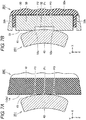
- Fig. 7A is a schematic sectional view illustrating an electric connecting structure of the main part in the remote terminal device of the first embodiment during the assembly operation
- Fig. 7B is a schematic sectional view illustrating the electric connecting structure in the main part in the remote terminal device after the assembly.
- the section in Fig. 7A is taken along a line VIIA-VIIA in Fig. 6A
- the section in Fig. 7B is taken along a line VIIB-VIIB in Fig. 6B .
- An assembly structure and an electric connecting structure of the remote terminal device 1 of the first embodiment will be described in detail below with reference to Figs. 6 and 7 .
- first unit 2B1 and a second unit 2B2 which are of two I/O units located adjacent to each other in the plurality of I/O units 2B of Fig. 1 .
- the first unit 2B1 is located on the left when the remote terminal device 1 is viewed from the front side (that is, viewed along the Y-axis direction), and the second unit 2B2 is located on the right when the remote terminal device 1 is viewed from the front side.
- the first unit 2B1 is assembled in the second unit 2B2 by inserting the first unit 2B1 in the second unit 2B2.
- the right side surface 13a that is of a first outer surface of the first unit 2B1 is moved toward a direction of an arrow AR from the front surface side so as to applied to the left side surface 13b that is of a second outer surface of the second unit 2B2.
- the upper and lower projecting streaks 16a and 16b that are of the pair of projecting streaks provided in the left side surface 13b of the second unit 2B2 are inserted in the upper and lower guide grooves 15a and 15b that are of the pair of guide grooves provided in the right side surface 13a of the first unit 2B1. Therefore, the first unit 2B1 is guided by the second unit 2B2, and slidably moved along the Y-axis direction.
- the first connecting terminal 40 is elastically deformed so as to recede toward the inside of the first unit 2B1 as illustrated in Fig. 7A , and the first connecting terminal 40 slides on an outer surface 14 of the casing 10 defining the left side surface 13b of the second unit 2B2.
- the bulging surface 41 bulging outward (that is, toward the second unit 2B2) is formed in the exposed surface of each of the plurality of first connecting terminals 40, the first connecting terminal 40 and the outer surface 14 of the casing 10 of the second unit 2B2 come into contact with each other at a point P1 corresponding to a top of the first connecting terminal 40 located on the side of the second unit 2B2 as illustrated in Fig. 7A .
- the first unit 2B1 is slidably moved until the first unit 2B1 comes to the position just beside the second unit 2B2, whereby the first terminal surface 31 of the first unit 2B1 is disposed at the position directly confronting the second terminal surface 32 of the second unit 2B2 when the first unit 2B1 is assembled in the second unit 2B2.
- the plurality of first connecting terminals 40 provided in the first unit 2B1 are in contact with the plurality of second connecting terminals 50 provided in the second unit 2B2, respectively.
- each of the plurality of first connecting terminals 40 is elastically deformable along the X-axis direction, the bulging surface 41 of the first connecting terminal 40 is partially fitted in the recess 52 of the second connecting terminal 50 based on restoring force of the first connecting terminal 40 as illustrated in Fig. 7B . Therefore, the first connecting terminal 40 comes into press-contact with the second connecting terminal 50 at two points corresponding to the pair of opening edges 52a that are located while facing each other in the Z-axis direction of the recess 52 of the second connecting terminal 50.
- parts of the bulging surface 41 of the first connecting terminal 40 come into press-contact with the pair of opening edges 52a, which are located while facing each other in the Z-axis direction of the recess 52 of the second connecting terminal 50, at points P2 and P3 in Fig. 7B , whereby the electric conduction between the first connecting terminal 40 and the second connecting terminal 50 is established at the contact portions.
- the first unit 2B1 can be removed from the second unit 2B2 by moving the first unit 2B1 toward the front surface from the assembly state in Fig. 6B (toward the direction opposite to the direction of the arrow AR in Fig. 6A ).
- the communication unit 2A is assembled in and removed from the I/O unit 2B continuously connected to the communication unit 2A in a way basically similar to the assembly and removal of the first unit 2B1 in and from the second unit 2B2.
- the remote terminal device 1 of the first embodiment can obtain the following effect compared with the conventional remote terminal device in which the exposed surface includes the flat surface without providing the recess in the exposed surface of the second connecting terminal.
- the first connecting terminal 40 slides on the outer surface 14 of the casing 10 in assembling the first unit 2B1 in the second unit 2B2, whereby the first connecting terminal 40 comes into contact with the outer surface 14 at the point P1.
- the first connecting terminal 40 comes into press-contact with the second connecting terminal 50 at the points P2 and P3 after the first unit 2B1 is assembled in the second unit 2B2.
- the contact point between the first connecting terminal 40 and the outer surface 14 of the casing 10 is located on the bulging surface 41 different from the contact point between the first connecting terminal 40 and the second connecting terminal 50.
- the first connecting terminal 40 catches a foreign substance such as dust adhering to the outer surface 14 of the casing 10 during the sliding, or catches shavings of a partially-scraped outer surface 14 of the casing 10, the foreign substance adheres to the point P1 of the first connecting terminal 40 or in a neighborhood of the point P1, and the foreign substance does not adhere to the points P2 and P3 that are of the contact portion between the first connecting terminal 40 and the second connecting terminal 50 in the neighborhood of the points P2 and P3.
- the foreign substance hardly enters the contact portion between the first connecting terminal 40 and the second connecting terminal 50, generation of a communication error due to blocking of the electric conduction between the first connecting terminal 40 and the second connecting terminal 50 can largely be prevented compared with the conventional remote terminal device described above.
- the first connecting terminal 40 and the second connecting terminal 50 come into contact with each other at the points P2 and P3 in the assembly state. Therefore, the electric conduction can be maintained between the first connecting terminal 40 and the second connecting terminal 50 when the foreign substance is not caught at one of the points P2 and P3 even if the foreign substance is caught at the other of the points P2 and P3.
- the generation of the communication error due to blocking of the electric conduction between the first connecting terminal 40 and the second connecting terminal 50 can largely be prevented compared with the conventional remote terminal device.
- the adoption of the configuration of the remote terminal device 1 increases a contact area between the first connecting terminal 40 and the second connecting terminal 50 to suppress a contact resistance between the first connecting terminal 40 and the second connecting terminal 50.
- the first connecting terminal 40 and the second connecting terminal 50 come into contact with each other at the two points corresponding to the pair of opening edges 52a of the recess 52 of the second connecting terminal 50 in the assembly state. Therefore, in the second connecting terminal 50, by virtue of a relatively angular shape of the contact point with the first connecting terminal 40, the first connecting terminal 40 and the second connecting terminal 50 are in contact with each other with a high contact pressure at the contact point.
- Elastic biasing force that is, a contact load
- Elastic biasing force applied onto the side of the second unit 2B2 can be lowered in the first connecting terminal 40 by increasing the contact pressure at the contact point between the first connecting terminal 40 and the second connecting terminal 50 as described above. Accordingly, frictional force that is generated when the first connecting terminal 40 slides on the outer surface 14 of the casing 10 while being contact with the outer surface 14 and frictional force that is generated when the first connecting terminal 40 slides on the second connecting terminal 50 while being contact with the second connecting terminal 50 can be lowered compared with the conventional remote terminal device. As a result, force necessary for the insertion and removal of the unit can be lowered even if the remote terminal device 1 of the first embodiment including the many first connecting terminals 40 and many second connecting terminals 50 is used.
- the blocking of the electric connection between the units can be prevented without lowering operability during the insertion and removal of the unit, and reliability of the electric connection between the units can be enhanced higher than before.
- Figs. 8A to 8G are schematic sectional views illustrating various modifications of the second connecting terminal in the remote terminal device of the first embodiment.
- the rectangular groove is formed as the recess 52 provided in the exposed surface 51 of the second connecting terminal 50.
- another configuration can be used.
- Fig. 8A illustrates the case that the recess 52 provided in the exposed surface 51 of the second connecting terminal 50 includes an inverted trapezoidal groove in which a pair of side surfaces is formed into an inclined shape.
- Fig. 8B illustrates the case that the recess 52 provided in the exposed surface 51 of the second connecting terminal 50 includes a V-shape groove.
- Fig. 8C illustrates the case that the recess 52 provided in the exposed surface 51 of the second connecting terminal 50 includes a semi-circular groove.
- Fig. 8D illustrates the case that the recess 52 provided in the exposed surface 51 of the second connecting terminal 50 includes a two-stage rectangular groove.
- the grooves having various sectional shapes can be used as the recess 52, and the above effect can be obtained in the case that any groove is used.
- Fig. 8E illustrates the case that the recess 52 provided in the exposed surface 51 of the second connecting terminal 50 includes not the groove but a through-hole.
- the recess 52 is not necessarily formed into the groove shape, but the through-hole can be made as the recess 52. The above effect can be obtained even if the configuration in Fig. 8E is used.
- Fig. 8F illustrates the case that a boundary between the exposed surface 51 and the recess 52, which defines the opening edge 52a of the recess 52, includes the inclined surface although the rectangular groove is used as the recess 52 provided in the exposed surface 51 of the second connecting terminal 50.
- Fig. 8G illustrates the case that the boundary between the exposed surface 51 and the recess 52, which define the opening edge 52a of the recess 52, includes a curved surface although the rectangular groove is used as the recess 52 provided in the exposed surface 51 of the second connecting terminal 50.
- the opening edge 52a of the recess 52 has various shapes, and the above effect can be obtained even if the configurations in Figs. 8F and 8G are used.
- Figs. 9A to 9E are schematic sectional views illustrating various modifications of the first connecting terminal in the remote terminal device of the first embodiment.
- the substantially flat first connecting terminal 40 in which the portion close to the leading end of the first connecting terminal 40 has the mountainously-curved shape along the Z-axis direction is used by way of example, the portion close to the leading end being in contact with the second connecting terminal 50.
- the first connecting terminal 40 having another shape may be used.
- Fig. 9A illustrates the case that the portion close to the leading end of the first connecting terminal 40 is partially bent in the Z-axis direction and formed into a V-shape in a sectional view, the portion close to the leading end being in contact with the second connecting terminal 50, and therefore the bulging surface 41 is formed.
- Fig. 9B illustrates the case that the portion close to the leading end of the first connecting terminal 40 is bent stepwise in the Z-axis direction, the portion close to the leading end being in contact with the second connecting terminal 50, and therefore the bulging surface 41 is formed.
- the bulging surface 41 of the first connecting terminal 40 is not necessarily bent, but the bulging surface 41 may be formed by a combination of the inclined surfaces. In such cases, the above effect can also be obtained.
- Fig. 9C illustrates the case that the bulging surface 41 is formed by providing a bulging portion having a trapezoidal shape in a sectional view in a part of the flat first connecting terminal 40.
- Fig. 9D illustrates the case that the bulging surface 41 is formed by providing a bulging portion having a mountainous shape in a sectional view in a part of the flat first connecting terminal 40.
- the bulging surface 41 of the first connecting terminal 40 is not necessarily formed by bending or folding the first connecting terminal 40, but the bulging surface 41 may be formed by locally shaping the bulging portion through pressing. In such cases, the above effect can also be obtained.
- Fig. 9E illustrates the case that the first connecting terminal 40 is formed by a pin-shaped or projection member projecting streak in the X-axis direction instead of the flat first connecting terminal 40 and that the leading end of the first connecting terminal 40 is formed into a semi-circular shape in a sectional view.
- a biasing spring or the like is provided so as to be engaged with the first connecting terminal 40, thereby providing the elasticity to the first connecting terminal 40.
- the first connecting terminal 40 does not necessarily have a plate spring shape, but the first connecting terminal 40 may be formed by a combination of the pin-shaped or projection member and the biasing spring. In such cases, the above effect can also be obtained.
- the bulging surface 41 provided in the first connecting terminal 40 in which the outwardly bulging amount varies in the Y-axis direction and the Z-axis direction is used by way of example.
- the outwardly bulging amount does not necessarily vary in the Y-axis direction, but the above effect can be obtained as long as the outwardly bulging amount varies in the Z-axis direction.
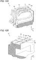
- Fig. 10A is a partially broken and perspective view illustrating a terminal block including a first connecting terminal of an I/O unit of a remote terminal device according to a second embodiment of the present invention
- Fig. 10B is a partially broken and perspective view illustrating the terminal block including a second connecting terminal of the I/O unit.
- a terminal block 30' included in the I/O unit of the remote terminal device of the second embodiment and the first connecting terminal 40 and second connecting terminal 50 included in the terminal block 30' will be described with reference to Fig. 5 .
- the terminal block 30' of the I/O unit of the remote terminal device has the configuration different from the first embodiment in the plurality of second connecting terminals 50 while having the configuration similar to the first embodiment in the plurality of first connecting terminals 40.
- the recess 52 provided in the exposed surface 51 at the leading end of each of the plurality of second connecting terminals 50 is formed into a rectangular groove shape extending along the Z-axis direction, and one recess 52 is provided at the central position in the Y-axis direction in the exposed surface 51 of the second connecting terminal 50. Therefore, in the exposed surfaces 51 of the plurality of second connecting terminals 50, the pair of opening edges 52a of the recess 52 is formed in parallel so as to extend along the Z-axis direction, and the pair of opening edges 52a of the recess 52 is located while facing each other in the Y-axis direction. The pair of opening edges 52a of the recess 52 is a boundary between the exposed surface 51 and the recess 52.
- Fig. 11A is a schematic sectional view illustrating an electric connecting structure of a main part in the remote terminal device of the second embodiment during the assembly operation
- Fig. 11B is a schematic sectional view illustrating the electric connecting structure of the main part in the remote terminal device after the assembly.
- the electric connecting structure of the remote terminal device of the second embodiment will be described in detail below with reference to Fig. 11 .
- the first connecting terminal 40 is elastically deformed so as to recede toward the inside of the first unit 2B1, and the first connecting terminal 40 slides on the outer surface 14 defining the left side surface 13b of the second unit 2B2 in the casing 10.
- the bulging surface 41 bulging outward (that is, toward the second unit 2B2) is formed in the exposed surface of each of the plurality of first connecting terminals 40, the first connecting terminal 40 and the outer surface 14 of the casing 10 of the second unit 2B2 come into contact with each other at a point P1 corresponding to a top of the first connecting terminal 40 located on the side of the second unit 2B2 as illustrated in Fig. 11A .
- parts of the bulging surface 41 of the first connecting terminal 40 come into press-contact with the pair of opening edges 52a, which are located while facing each other in the Y-axis direction of the recess 52 of the second connecting terminal 50, at points P4 and P5 in Fig. 7B , whereby the electric conduction between the first connecting terminal 40 and the second connecting terminal 50 is established at the contact portions.
- the effect substantially similar to that of the first embodiment is obtained, the blocking of the electric connection between the units can be prevented without lowering the operability during the insertion and removal of the unit, and the reliability of the electric connection between the units can be enhanced higher than before.
- the grooves or through-holes having various sectional shapes can be formed as the recess 52 provided in the exposed surface 51 of the second connecting terminal 50 similarly to the first embodiment.
- the first connecting terminal 40 of the portion being in contact with the second connecting terminal 50 is not limited to the bulging surface 41 including the curved surface formed by the bending, but the bulging surface 41 may include the folded surface formed by the folding, the bulging surface 41 may be constructed by locally providing the bulging portion through the pressing, or the bulging surface 41 may be constructed by the combination of the pin-shaped or projection member and the biasing spring.
- the bulging surface 41 provided in the first connecting terminal 40 in which the outwardly bulging amount varies in the Y-axis direction and the Z-axis direction is used by way of example.
- the outwardly bulging amount does not necessarily vary in the Z-axis direction, but the above effect can be obtained as long as the outwardly bulging amount varies in the Y-axis direction.
- Figs. 12A to 12H are plan views illustrating other modifications of the second connecting terminal in the remote terminal devices according to the first and second embodiments of the present invention.
- Fig. 12A illustrates the case that the plurality of recesses 52, each of which is provided in the exposed surface 51 of the second connecting terminal 50 so as to extend along the Y-axis direction in the first embodiment, are formed in the Z-axis direction.
- the above effect can be obtained by fitting the bulging surface 41 of the first connecting terminal 40 in one of the recesses 52.
- the plurality of bulging surfaces 41 corresponding to the number of recesses 52 are provided along the Z-axis direction in the first connecting terminal 40, and each of the bulging surfaces 41 may be formed so as to be fitted in the recess 52.
- the number of contact portions between the first connecting terminal 40 and the second connecting terminal 50 increases to be able to further improve the reliability of the electric connection.
- Fig. 12B illustrates the case that the recess 52, which is provided in the exposed surface 51 of the second connecting terminal 50 so as to extend along the Y-axis direction in the first embodiment, includes a groove having a rectangular shape in a plan view such that both ends of the recess 52 are interrupted at middle positions in the exposed surface 51 of the second connecting terminal 50. In this case, the similar effect can also be obtained.
- Fig. 12C illustrates the case that the recess 52, which is provided in the exposed surface 51 of the second connecting terminal 50 so as to extend along the Y-axis direction in the first embodiment, includes a groove having an oval shape in a plan view such that both ends of the recess 52 are interrupted at middle positions in the exposed surface 51 of the second connecting terminal 50. In this case, the similar effect can also be obtained.
- Fig. 12D illustrates the case that the plurality of recesses 52, each of which is provided in the exposed surface 51 of the second connecting terminal 50 so as to extend along the Z-axis direction in the second embodiment, are formed in the Y-axis direction.
- the above effect can be obtained by fitting the bulging surface 41 of the first connecting terminal 40 in one of the recesses 52.
- the plurality of bulging surfaces 41 corresponding to the number of recesses 52 are provided along the Y-axis direction in the first connecting terminal 40, and each of the bulging surfaces 41 may be formed so as to be fitted in the recess 52.
- the number of contact portions between the first connecting terminal 40 and the second connecting terminal 50 increases to be able to further improve the reliability of the electric connection.
- Fig. 12E illustrates the case that the recess 52, which is provided in the exposed surface 51 of the second connecting terminal 50 in the first and second embodiments, includes a groove having a lattice shape in a plan view while including a plurality of grooves extending along the Y-axis direction and a plurality of grooves extending along the Z-axis direction.
- the above effect can be obtained by fitting the bulging surface 41 of the first connecting terminal 40 in any one of portions of the lattice-shape recesses 52.
- the exposed surface of the first connecting terminal 40 is unevenly formed so as to include the plurality of bulging surfaces 41, and each of the bulging surfaces 41 may be formed so as to be fitted in any one of portions of the lattice-shape recess 52.
- the number of contact portions between the first connecting terminal 40 and the second connecting terminal 50 increases to be able to further improve the reliability of the electric connection.
- Fig. 12F illustrates the case that the recess 52, which has the lattice shape in a plan view like the configuration in Fig. 12E while including a plurality of grooves intersecting each other, is disposed such that the plurality of grooves of the recess 52 intersect the Y-axis direction of the unit inserting and removing direction.
- the above effect can be obtained by fitting the bulging surface 41 of the first connecting terminal 40 in any one of portions of the lattice-shape recesses 52.
- the exposed surface of the first connecting terminal 40 is unevenly formed so as to include the plurality of bulging surfaces 41, and each of the bulging surfaces 41 may be formed so as to be fitted in any one of portions of the lattice-shape recess 52.
- Fig. 12G illustrates the case that the recess 52, which is provided in the exposed surface 51 of the second connecting terminal 50 so as to extend along the Y-axis direction or Z-axis direction in the first and second embodiments, includes a spot-like recess having a rectangular shape in a plan view.
- the first connecting terminal 40 in which the bulging surface 41 is curved into the mountainous shape along both the Y-axis direction and the Z-axis direction is press-contact with the recess 52 at the pair of opening edges 52a facing each other in the Y-axis direction and the pair of opening edges 52a facing each other in the Z-axis direction. Therefore, the similar effect can be obtained, and the reliability of the electric connection can further be improved by increasing the number of contact portions between the first connecting terminal 40 and the second connecting terminal 50.
- Fig. 12H illustrates the case that the recess 52 provided in the exposed surface 51 of the second connecting terminal 50 includes a spot-like recess having a circular shape in a plan view.
- the similar effect can be obtained when the shape of the bulging surface 41 is formed into a semi-spherical shape in the first connecting terminal 40 based on the shape of the opening edge 52a of the recess 52 formed into the circular shape in a plan view.
- the first connecting terminal and the second connecting terminal are in press-contact with each other only at the position corresponding to the opening edge of the recess of the second connecting terminal in the assembly state.
- the first connecting terminal and the second connecting terminal may be in press-contact with each other in a partial bulging surface of the first connecting terminal and a partial inner surface of the recess in the portion in which the first connecting terminal is fitted in the recess of the second connecting terminal.
- the top of the bulging surface of the first connecting terminal may be in further contact with a bottom of the recess.
- the first connecting terminal is elastically deformable.
- the second connecting terminal may be elastically deformable in addition to the first connecting terminal.
- the present invention is applied to the remote terminal device provided with the I/O units having the identical shape and configuration.
- the I/O units continuously connected to each other do not necessarily have the identical shape and configuration.
- the present invention can be applied to the remote terminal device provided with the continuously-connected I/O units having different widths.
- the present invention is applied to the remote terminal device attached to the DIN rail.
- the present invention is not limited to the remote terminal device attached to the DIN rail.
- the present invention is applied to the remote terminal device of the PLC.
- the present invention is not limited to the remote terminal device of the PLC, but the present invention can also be applied to various electric device systems including at least a pair of electric device units, which are electrically connected to each other while assembled side by side.
Landscapes
- Engineering & Computer Science (AREA)
- Automation & Control Theory (AREA)
- Microelectronics & Electronic Packaging (AREA)
- Connections Arranged To Contact A Plurality Of Conductors (AREA)
- Casings For Electric Apparatus (AREA)
- Coupling Device And Connection With Printed Circuit (AREA)
Description
- The present invention relates to an electric device system including a plurality of electric device units.
- Conventionally, there are various electric device systems including a plurality of electric device units. There is well known an electric device system including the plurality of electric device units, which are electrically connected to each other by assembling the electric device units in line along a predetermined direction. A remote terminal device (hereinafter, also simply referred to as a remote terminal device) of a Programmable Logic Controller (PLC) can be cited as a typical example of the electric device system having the configuration.
- The remote terminal device includes a communication unit and one or more I/O unit that can conduct communication with the communication unit through a serial bus line and a unidirectional communication line, and the communication unit and the I/O unit are generally formed into a building block type such that the I/O units are provided in the communication unit while continuously connected to each other.
- For example,
JP 6-6051 A JP2001-217016 A JP 2012-182412 A - Frequently, each of the communication unit and I/O unit, which are of the electric device unit, is attached to an attaching rail such as a DIN (German industry standard) rail, and the adjacent electric device units are assembled so as to be engaged with each other.
- In such cases, generally a guide groove and a projecting streak that are of a guiding mechanism are provided in a pair of electric device units adjacent to each other, and the projecting streak provided in one of the pair of electric device units is slidably guided by the guide groove provided in the other, whereby the pair of electric device units are detachably engaged with each other. For example,
JP2001-217016 A JP 2012-182412 A
WO 97/10692 A1
EP 1 798 822 A1
US 2006/0205290 A1 describes a connection contact of an electric connector. A groove is formed on a connecting section surface of an electrically conductive terminal, this groove is subjected to a bending deformation into a convex shape toward the surface side from the backside of a connecting section to form a bent convex section on the surface of the connecting terminal, and edge sections formed on both sides of this groove are positioned on the surface of the bent convex section.
JP 2007 080843 A
JP 2007 053066 A
US 2013/0045617 A1 describes a method for manufacturing a metal component including the steps of forming a resist film on a surface of an electrode plate, making the resist film exposed to light by use of a photomask having a mask pattern, in at least part of a rim of which a fine concavity and convexity are drawn, developing the resist film, to form an opening for molding in the resist film, and epositing an electroforming material by electroforming inside the opening for molding, to mold the material.
JP 2001 043920 A
JP 2009 193733 A
US 2014/0099803 A1 describes an electrical contact assembly including a first electrical contact having a first mating element, and a second electrical contact having a second mating element. The first and second electrical contacts being configured to mate together at the first and second mating elements such that the first and second mating elements engage each other at a contact interface. A distribution of contact pressure across the contact interface at least partially coincides with a distribution of electrical current flow across the contact interface. - In the electric device system including the electric device unit in which the guiding mechanism is provided, a first connecting terminal and a second connecting terminal are provided at positions corresponding to outer surfaces of the pair of electric device units adjacent to each other in order to establish the electric connection. Therefore, the first and second connecting terminals are in contact with each other while one of the pair of electric device units is assembled in the other, thereby establishing the electric connection between the electric device units.
- In this case, in order to ensure electric conduction between the first and second connecting terminals, it is necessary that at least one of the first and second connecting terminals be provided so as to project from the outer surface of the electric device unit in a non-assembly state, and that at least one of the first and second connecting terminals be configured in an elastically deformable manner in a direction orthogonal to the outer surface.
- However, when one of the pair of electric device units is assembled in the other, because one of the connecting terminals projecting from the outer surface of the electric device unit slides on the outer surface of the other connecting terminal, possibly one of the connecting terminals catches a foreign substance such as dust adhering to a casing in the sliding, or catches shavings of a partially-scraped surface of the casing. In such cases, after one of the pair of electric device units is assembled in the other, the foreign substance penetrates between the first and second connecting terminals to block the electric conduction between the first and second connecting terminals, which results in generation of a communication error.
- Because the foreign substance is located near a contact point of the first and second connecting terminals even if the foreign substance does not penetrate between the first and second connecting terminals after one of the pair of electric device units is assembled in the other, when impact is applied to the electric device unit from the outside, the foreign substance penetrates between the first and second connecting terminals due to variation of a relative position between the first and second connecting terminals, which causes the electric conduction to be blocked between the first and second connecting terminals to generate the communication error.
- An object of the present invention is to provide an electric device system that can prevent blocking of the electric connection between the electric device units.
- An electric device system according to one aspect of the present invention is disclosed by
claim 1 and includes a plurality of electric device units, which are electrically connected to each other by assembling the electric device units in line along a first direction. The plurality of electric device units include a first unit and a second unit, which are adjacent to each other in an assembly state, and each of the first unit and the second unit includes an insulating casing as an outer shell. A first connecting terminal is provided at a predetermined position in a first outer surface that is a casing surface of the first unit, the casing surface of the first unit facing the second unit in the assembly state, at least a part of the first connecting terminal projecting from the first outer surface in a non-assembly state, the first connecting terminal being elastically deformable in the first direction, and a second connecting terminal is provided at a position in a second outer surface that is a casing surface of the second unit, the casing surface of the second unit facing the first unit in the assembly state, the position in the second outer surface facing the first connecting terminal in the assembly state. A guiding mechanism is provided in the first unit and the second unit, the guiding mechanism slidably guiding the first unit into the second unit along a second direction orthogonal to the first direction to enable the first unit to be assembled in and removed from the second unit, and the guiding mechanism guides the first unit into the second unit in assembling the first unit in the second unit such that the first connecting terminal comes into contact with the second connecting terminal after sliding on the second outer surface. A bulging surface bulging out toward the second unit is provided on an exposed surface of the first connecting terminal located on the second unit side in the assembly state, and a recess is provided on an exposed surface of the second connecting terminal located on the first unit side in the assembly state. In the electric device system, a part of the bulging surface is fitted in the recess in the assembly state, and therefore at least the part of the bulging surface comes into press-contact with at least a part of an opening edge of the recess to establish electric conduction between the first connecting terminal and the second connecting terminal. - In the electric device system, the bulging surface bulges out such that a bulging amount toward the second unit varies in a third direction orthogonal to the first direction and the second direction, and the recess includes a pair of opening edges facing each other in the third direction. In this case, the first connecting terminal and the second connecting terminal come into press-contact with each other at two points corresponding to the pair of opening edges of the recess in the assembly state. In this case, the recess may include a groove extending along the second direction.
- In the electric device system, the bulging surface may bulge out such that a bulging amount toward the second unit varies in the second direction, and the recess may include a pair of opening edges facing each other in the second direction. In this case, the first connecting terminal and the second connecting terminal come into press-contact with each other at two points corresponding to the pair of opening edges of the recess in the assembly state. In this case, the recess may include a groove extending along a third direction orthogonal to both the first direction and the second direction.
- In the electric device system, the bulging surface may bulge out such that a bulging amount toward the second unit varies in a third direction orthogonal to the first direction and the second direction while the bulging surface bulges out such that a bulging amount toward the second unit varies in the second direction, and the recess may include a pair of opening edges facing each other in the second direction and a pair of opening edges facing each other in the third direction. In this case, the first connecting terminal and the second connecting terminal come into press-contact with each other at four points corresponding to the four opening edges of the recess in the assembly state.
- In the electric device system, the recess may include a recessed portion including an opening edge having a cyclic shape in a plan view. In this case, preferably the bulging surface has a shape corresponding to the opening edge, and the first connecting terminal and the second connecting terminal are in press-contact with each other in a whole circumference of the opening edge in the assembly state.
- In the electric device system, the first unit and the second unit may be assembled by attaching the first unit and the second unit to an attaching rail extending along the first direction. In this case, preferably a direction in which the first unit and the second unit are attached to the attaching rail is aligned with the second direction.
- In the electric device system, the plurality of electric device units may further include one or more electric device units in addition to the first unit and the second unit. In this case, preferably all pairs of electric device units located adjacent to each other in the plurality of electric device units have an electric connecting structure identical to electric connecting structures of the first unit and the second unit.
- Accordingly, the present invention can provide the electric device system that can prevent the blocking of electric connection between electric device units.
-
-
Fig. 1 is a perspective view illustrating an assembly state of a remote terminal device according to a first embodiment of the present invention; -
Fig. 2A is a perspective view illustrating a front surface of an I/O unit inFig. 1 when the I/O unit is viewed from an upper right,Fig. 2B is an enlarged perspective view illustrating a main part of the I/O unit, andFig. 2C is an enlarged right side view illustrating the main part of the I/O unit; -
Fig. 3A is a perspective view illustrating a front surface of the I/O unit inFig. 1 when the I/O unit is viewed from an upper left,Fig. 3B is an enlarged perspective view illustrating the main part of the I/O unit, andFig. 3C is an enlarged left side view illustrating the main part of the I/O unit; -
Fig. 4A is a front view of the I/O unit inFig. 1 , andFig. 4B is a sectional view of the I/O unit; -
Fig. 5A is a partially broken and perspective view illustrating a terminal block including a first connecting terminal of the I/O unit inFig. 1 , andFig. 5B is a partially broken and perspective view illustrating the terminal block including a second connecting terminal of the I/O unit; -
Fig. 6A is a schematic sectional view illustrating an assembly structure of the remote terminal device according to the first embodiment of the present invention during assembly operation, andFig. 6B is a schematic sectional view illustrating the assembly structure of the remote terminal device after assembly; -
Fig. 7A is a schematic sectional view illustrating an electric connecting structure of the main part in the remote terminal device according to the first embodiment of the present invention during the assembly operation, andFig. 7B is a schematic sectional view illustrating the electric connecting structure of the main part in the remote terminal device after the assembly; -
Figs. 8A to 8G are schematic sectional views illustrating various modifications of the second connecting terminal in the remote terminal device according to the first embodiment of the present invention; -
Figs. 9A to 9E are schematic sectional views illustrating various modifications of the first connecting terminal in the remote terminal device according to the first embodiment of the present invention; -
Fig. 10A is a partially broken and perspective view illustrating a terminal block including a first connecting terminal of an I/O unit in a remote terminal device according to a second embodiment of the present invention, andFig. 10B is a partially broken and perspective view illustrating the terminal block including a second connecting terminal of the I/O unit; -
Fig. 11A is a schematic sectional view illustrating an electric connecting structure of a main part in the remote terminal device according to the second embodiment of the present invention during the assembly operation, andFig. 11B is a schematic sectional view illustrating the electric connecting structure of the main part in the remote terminal device after the assembly; and -
Figs. 12A to 12H are plan views illustrating various modifications of the second connecting terminal in the remote terminal devices according to the first and second embodiments of the present invention. - Hereinafter, embodiments of the present invention will be described with reference to the drawings. In the following embodiments, a remote terminal device of a PLC is illustrated as an example of an electric device system to which the present invention is applied. In the following embodiments, the identical or common component is designated by the identical numeral in the drawings, and the overlapping description is omitted.
-
Fig. 1 is a perspective view illustrating an assembly state of a remote terminal device according to a first embodiment of the present invention. A configuration of a remoteterminal device 1 of the first embodiment will be described below with reference toFig. 1 . - As illustrated in
Fig. 1 , the remoteterminal device 1 includes acommunication unit 2A, a plurality of I/O units 2B, and an end cover 3. Thecommunication unit 2A, the plurality of I/O units 2B, and the end cover 3 are assembled so as to be arrayed along an X-axis direction of a first direction. Thecommunication unit 2A and the plurality of I/O units 2B correspond to a plurality ofelectric device units 2 constituting the remoteterminal device 1 that is of the electric device system. In the first embodiment, the plurality of I/O units 2B have an identical shape and an identical configuration. - The
communication unit 2A is disposed on a leftmost side when the remoteterminal device 1 is viewed from a front surface side (viewed along a Y-axis direction of a second direction), and the end cover 3 is disposed on a rightmost side when the remoteterminal device 1 is viewed from the front surface side. The plurality of I/O units 2B are disposed between thecommunication unit 2A and end cover 3, which are disposed at both ends of the I/O units 2B, so as to be continuously connected to each other. - The
communication unit 2A is connected to a plurality of I/O units 2B through a serial bus line and a unidirectional communication line, and exchanges control data with each of the plurality of I/O units 2B. Thecommunication unit 2A is connected to an externally-installed PLC (not illustrated) through a cable (not illustrated), and exchanges the control data with the PLC. Thecommunication unit 2A is also equipped with a power supply circuit and a CPU that controls an IN device and an OUT device. - As described above, each of the plurality of I/
O units 2B is connected to thecommunication unit 2A through the serial bus line and the unidirectional communication line, and exchanges the control data with thecommunication unit 2A. Each of the plurality of I/O units is connected to a sensor and a switch (not illustrated) that are of the IN device and an actuator (not illustrated) that is of the OUT device through a cable (not illustrated), and exchanges the control data with the IN device and the OUT device. - The end cover 3 is a decorative cover that covers an exposed right side surface of the I/
O unit 2B, which is located on the rightmost side in the plurality of I/O units 2B when the remoteterminal device 1 is viewed from the front surface side. - The
communication unit 2A and the plurality of I/O units 2B are attached to aDIN rail 100 of an attaching rail with a fixing member interposed therebetween. In thecommunication unit 2A and the plurality of I/O units 2B, the adjacent units are engaged with each other while a guiding mechanism provided in each unit is interposed therebetween, the I/O unit 2B located on the rightmost side in the plurality of I/O units 2B and the end cover 3 are also engaged with each other while the guiding mechanism provided in each unit is interposed therebetween. Therefore, thecommunication unit 2A, the plurality of I/O units 2B, and the end cover 3 are integrally attached to theDIN rail 100. - In the remote
terminal device 1 having the above configuration, each of the IN device and OUT device that are connected to the plurality of I/O units 2B conducts communication with the CPU provided in thecommunication unit 2A, thereby controlling a whole facility to which the remoteterminal device 1 is attached. Because the remoteterminal device 1 is controlled by the externally-installed PLC, the PLC can integrally control all the plurality of facilities by installing the plurality of remoteterminal devices 1 in each facility. - At this point, the plurality of I/
O units 2B can be installed as many as the IN devices and OUT devices that are included in the facility to which the remoteterminal device 1 is attached. InFig. 1 , although the remoteterminal device 1 includes eight I/O units 2B in total, the number of I/O units 2B can be increased and decreased based on the facility to which the remoteterminal device 1 is attached. -
Fig. 2A is a perspective view illustrating a front surface of the I/O unit inFig. 1 when the I/O unit is viewed from an upper right,Fig. 2B is an enlarged perspective view illustrating a main part of the I/O unit, andFig. 2C is an enlarged right side view illustrating the main part of the I/O unit.Fig. 3A is a perspective view illustrating a front surface of the I/O unit inFig. 1 when the I/O unit is viewed from an upper left,Fig. 3B is an enlarged perspective view illustrating the main part of the I/O unit, andFig. 3C is an enlarged left side view illustrating the main part of the I/O unit.Fig. 4A is a front view of the I/O unit inFig. 1 , andFig. 4B is a sectional view taken on a line IVB-IVB inFig. 4A . The configuration of the I/O unit 2B will be described below with reference toFigs. 2 to 4 . - As illustrated in
Figs. 2 to 4 , the I/O unit 2B has a flat, substantially rectangular parallelepiped external form in which a width in a horizontal width is narrowed. Afront surface 11a, arear surface 11b, atop surface 12a, abottom surface 12b, aright side surface 13a, and aleft side surface 13b of the I/O unit 2B having the substantially rectangular parallelepiped shape are defined by an insulatingcasing 10 that is of an outer shell. - A plurality of sockets are provided in the
front surface 11a of the I/O unit 2B in order to connect the IN device and OUT device to the I/O unit 2B. An end of the cable connected to the IN device or OUT device can be inserted in each of the plurality of sockets, and the inserted end of the cable is held by the socket to provide the electric connection between the I/O unit 2B and the IN device or OUT device. - A fixing
member 20 is assembled in therear surface 11b of the I/O unit 2B in order to attach the I/O unit 2B to theDIN rail 100. The fixingmember 20 includes an operatingknob 21, aslider 22, and anupper latching pawl 23a and alower latching pawl 23b that are of a pair of latching pawls. The fixingmember 20 is configured such that the upper andlower latching pawls knob 21. Therefore, the operatingknob 21 is vertically moved while therear surface 11b of the I/O unit 2B is applied to theDIN rail 100, which allows the I/O unit 2B to be detachably attached to theDIN rail 100. - An
upper guide groove 15a and alower guide groove 15b, which are of a pair of guide grooves, are provided in theright side surface 13a of the I/O unit 2B. Theupper guide groove 15a is provided near an end side located on the side of thetop surface 12a in theright side surface 13a of the I/O unit 2B, and extends along the Y-axis direction. Thelower guide groove 15b is provided near an end side located on the side of thebottom surface 12b in theright side surface 13a of the I/O unit 2B, and extends along the Y-axis direction. The upper guide andlower guide grooves - An upper projecting
streak 16a and a lower projectingstreak 16b, which are of a pair of projecting streaks, are provided in theleft side surface 13b of the I/O unit 2B. The upper projectingstreak 16a is provided near an end side located on the side of thetop surface 12a in theleft side surface 13b of the I/O unit 2B, and extends along the Y-axis direction. The lower projectingstreak 16b is provided near the end side located on the side of thebottom surface 12b in theleft side surface 13b of the I/O unit 2B, and extends along the Y-axis direction. The upper projectingstreak 16a projects upward along the Z-axis direction, and the lower projectingstreak 16b projects downward along the Z-axis direction. - Although the detailed description is omitted, a pair of guide grooves similar to the upper and
lower guide grooves right side surface 13a of the I/O unit 2B is also provided in the right side surface of thecommunication unit 2A, and a pair of guide grooves similar to the upper and lower projectingstreak left side surface 13b of the I/O unit 2B is provided in the left side surface of the end cover 3. - The upper and
lower guide grooves right side surface 13a of the I/O unit 2B, receive the upper and lower projecting streaks, which are of the pair of projecting streaks provided in the left side surface of the I/O unit 2B or end cover 3 that is disposed while continuously connected on the right side of the I/O unit 2B. The upper and lower projectingstreaks left side surface 13b of the I/O unit 2B, are received by the upper and lower guide grooves, which are of the pair of guide grooves provided in the right side surface of the I/O unit 2B orcommunication unit 2A that is disposed while continuously connected on the left side of the I/O unit 2B. - That is, the pair of guide grooves and the pair of projecting streaks correspond to the guiding mechanism that engages the
adjacent communication unit 2A, a plurality of I/O units 2B, and end cover 3 each two of which are located adjacent to each other. The pair of projecting streaks is slidably guided along the Y-axis direction by the pair of guide grooves, whereby thecommunication unit 2A, the plurality of I/O units 2B, and the end cover 3 can be separately inserted in and removed from the remoteterminal device 1 while the engagement is performed. - As illustrated in
Fig. 4B , aterminal block 30 and awiring circuit board 60 are mainly stored in thecasing 10 of the I/O unit 2B. Theterminal block 30 and thewiring circuit board 60 are held by thecasing 10 while stored in thecasing 10. - The
terminal block 30 includes a plurality of first connectingterminals 40 and a plurality of second connecting terminals 50 (seeFigs. 2 and3 ), and the plurality of first connectingterminals 40 and the plurality of second connectingterminals 50 are electrically connected to a plurality of conductive lines provided corresponding to thewiring circuit boards 60, respectively. Theterminal block 30 includes a firstterminal surface 31 on which the plurality of first connectingterminals 40 are exposed and a secondterminal surface 32 on which the plurality of second connectingterminals 50 are exposed. Theterminal block 30 is stored in a space of thecasing 10, and the space is located on the sides of therear surface 11b andtop surface 12a of the I/O unit 2B. - The
wiring circuit board 60 mainly includes the plurality of conductive lines, is connected to the plurality of first connectingterminals 40 and the plurality of second connectingterminals 50, and is connected to the plurality of sockets provided in thefront surface 11a of the I/O unit 2B. Thewiring circuit board 60 is stored in a space of thecasing 10 so as to be located in front of theterminal block 30. - At this point, the electric conduction is established among the plurality of first connecting
terminals 40 and the plurality of second connectingterminals 50, the plurality of conductive lines provided in thewiring circuit board 60, and the plurality of sockets, and the first and second connectingterminals - As illustrated in
Fig. 2 , afirst window 17a is formed at a predetermined position of theright side surface 13a of the I/O unit 2B by partially notching thecasing 10, and theterminal block 30 is disposed so as to face thefirst window 17a. The firstterminal surface 31 of theterminal block 30 is provided at a position corresponding to thefirst window 17a, and the firstterminal surface 31 is exposed outward to expose the plurality of first connectingterminals 40. - The first
terminal surface 31 of theterminal block 30 extends along the Z-axis direction, and the plurality of first connectingterminals 40 are arrayed in the Z-axis direction at predetermined intervals. The plurality of first connectingterminals 40 are located so as to partially project outward from theright side surface 13a of the I/O unit 2B (particularly, seeFigs. 2B ,4A, and 4B ). - As illustrated in
Fig. 3 , asecond window 17b is formed at a predetermined position of theleft side surface 13b of the I/O unit 2B by partially notching thecasing 10, and theterminal block 30 is disposed so as to face thesecond window 17b. The secondterminal surface 32 of theterminal block 30 is provided at a position corresponding to thesecond window 17b, and the secondterminal surface 32 is exposed outward to expose the plurality of second connectingterminals 50. - The second
terminal surface 32 of theterminal block 30 extends along the Z-axis direction, and the plurality of second connectingterminals 50 are arrayed along the Z-axis direction at predetermined intervals. The plurality of second connectingterminals 50 are located so as to be substantially flush with theleft side surface 13b of the I/O unit 2B (particularly, seeFigs. 3B and4B ). - Although the detailed description is omitted, a terminal block having a configuration similar to the portion including the first
terminal surface 31 of theterminal block 30 provided in the I/O unit 2B is also stored in the casing of thecommunication unit 2A, a plurality of first connecting terminals are provided in the terminal block, and the plurality of first connecting terminals are exposed on the right side surface of thecommunication unit 2A. - In the I/
O unit 2B, the first and second terminal surfaces 31 and 32 of theterminal block 30 are provided at positions corresponding to the right and left side surfaces 13a and 13b, respectively, of the I/O unit 2B. In thecommunication unit 2A, the first terminal surface of the terminal block is provided at a position corresponding to the secondterminal surface 32 provided in theleft side surface 13b of the I/O unit 2B that is disposed while continuously connected to thecommunication unit 2A. - In the assembly state of
Fig. 1 , the firstterminal surface 31 of one of the pair of adjacent units in thecommunication unit 2A and a plurality of I/O units 2B and the secondterminal surface 32 of the other unit are located so as to face each other, whereby the plurality of first connectingterminals 40 disposed in the firstterminal surface 31 of one of the adjacent units and the plurality of second connectingterminals 50 disposed in the secondterminal surface 32 of the other unit are in contact with each other, respectively. Accordingly, the pair of adjacent units are electrically connected to each other, and the remoteterminal device 1 includes thecommunication unit 2A and a plurality of I/O units 2B that are electrically connected to one another. -
Fig. 5A is a partially broken and perspective view illustrating the terminal block including the first connecting terminal of the I/O unit inFig. 1 , andFig. 5B is a partially broken and perspective view illustrating the terminal block including the second connecting terminal of the I/O unit. The detailed configurations of theterminal block 30 and the first connectingterminal 40 and second connectingterminal 50 that are included in theterminal block 30 will be described below with reference toFig. 5 . - As illustrated in
Fig. 5A , a plurality of groove-shaped first connectingterminal storage parts 31a extending along the Y-axis direction are arrayed along the Z-axis direction at predetermined intervals in the firstterminal surface 31 of theterminal block 30. A long and thin, substantially flat first connectingterminal 40 to which bending is subjected is stored in each of the plurality of first connectingterminal storage parts 31a, and the plurality of first connectingterminals 40 are separated from each other by an insulatingpartition wall 31b located between the first connectingterminals 40. - Each of the plurality of first connecting
terminals 40 is subjected to the bending to extend a portion close to a leading end of the first connectingterminal 40 along the substantial Y-axis direction, and the portion close to the leading end projects outward (that is, toward the X-axis direction) from the first connectingterminal storage part 31a. - In the portion projecting streak from the first connecting
terminal storage part 31a, a portion close to the leading end of the first connectingterminal 40 is formed into a shape bulging outward, thereby forming a bulgingsurface 41 in an exposed surface of a region facing the outside of the portion close to the leading end. - At this point, the bulging
surface 41 is bulged such that an outwardly bulging amount varies in the Y-axis direction, and such that an outwardly bulging amount varies in the Z-axis direction. More particularly, the bulgingsurface 41 is curved into a mountainous shape along both the Y-axis direction and the Z-axis direction. - As described above, each of the plurality of first connecting
terminals 40 is subjected to the bending, which provides elasticity to the first connectingterminal 40. Particularly, the first connectingterminal 40 is configured so as to be elastically deformable in the X-axis direction. - On the other hand, as illustrated in
Fig. 5B , a plurality of groove-shaped second connectingterminal storage parts 32a extending along the Y-axis direction are also arrayed along the Z-axis direction at predetermined intervals in the secondterminal surface 32 of theterminal block 30. A long and thin, substantially flat second connectingterminal 50 to which the bending is subjected is stored in each of the plurality of second connectingterminal storage parts 32a, and the plurality of second connectingterminals 50 are separated from each other by an insulatingpartition wall 32b located between the second connectingterminals 50. - An exposed
surface 51 at the leading end of each of the plurality of second connectingterminals 50 is formed into a substantially flat surface, and arecess 52 is provided at a predetermined position of the exposedsurface 51.
Therecess 52 is formed by a rectangular groove extending along the Y-axis direction, and therecess 52 is provided at a central position in the Z-axis direction of the exposedsurface 51 of the second connectingterminal 50. In the exposed surfaces 51 of the plurality of second connectingterminals 50, a pair of openingedges 52a of therecess 52 is formed in parallel so as to extend along the Y-axis direction, and the pair of openingedges 52a of therecess 52 is located while facing each other in the Z-axis direction. The pair of openingedges 52a of therecess 52 is a boundary between the exposedsurface 51 and therecess 52. - As described above, the terminal block having the configuration similar to the portion including the first
terminal surface 31 of theterminal block 30 provided in the I/O unit 2B is also provided in thecommunication unit 2A. The detailed configuration of the terminal block is similar to that inFig. 5A . -
Fig. 6A is a schematic sectional view illustrating an assembly structure of the remote terminal device of the first embodiment during assembly operation, andFig. 6B is a schematic sectional view illustrating the assembly structure of the remote terminal device after assembly.Fig. 7A is a schematic sectional view illustrating an electric connecting structure of the main part in the remote terminal device of the first embodiment during the assembly operation, andFig. 7B is a schematic sectional view illustrating the electric connecting structure in the main part in the remote terminal device after the assembly. At this point, the section inFig. 7A is taken along a line VIIA-VIIA inFig. 6A , and the section inFig. 7B is taken along a line VIIB-VIIB inFig. 6B . An assembly structure and an electric connecting structure of the remoteterminal device 1 of the first embodiment will be described in detail below with reference toFigs. 6 and7 . - The following description focuses only on a first unit 2B1 and a second unit 2B2, which are of two I/O units located adjacent to each other in the plurality of I/
O units 2B ofFig. 1 . The first unit 2B1 is located on the left when the remoteterminal device 1 is viewed from the front side (that is, viewed along the Y-axis direction), and the second unit 2B2 is located on the right when the remoteterminal device 1 is viewed from the front side. By way of example, the first unit 2B1 is assembled in the second unit 2B2 by inserting the first unit 2B1 in the second unit 2B2. - As illustrated in
Fig. 6A , in assembling the first unit 2B1 in the second unit 2B2, theright side surface 13a that is of a first outer surface of the first unit 2B1 is moved toward a direction of an arrow AR from the front surface side so as to applied to theleft side surface 13b that is of a second outer surface of the second unit 2B2. At this point, the upper and lower projectingstreaks left side surface 13b of the second unit 2B2 are inserted in the upper andlower guide grooves right side surface 13a of the first unit 2B1. Therefore, the first unit 2B1 is guided by the second unit 2B2, and slidably moved along the Y-axis direction. - At this point, the plurality of first connecting
terminals 40 provided so as to project from theright side surface 13a of the first unit 2B1 interferes with thecasing 10 of the second unit 2B2. However, as described above, because each of the plurality of first connectingterminals 40 is elastically deformable along the X-axis direction, the first connectingterminal 40 is elastically deformed so as to recede toward the inside of the first unit 2B1 as illustrated inFig. 7A , and the first connectingterminal 40 slides on anouter surface 14 of thecasing 10 defining theleft side surface 13b of the second unit 2B2. - As described above, because the bulging
surface 41 bulging outward (that is, toward the second unit 2B2) is formed in the exposed surface of each of the plurality of first connectingterminals 40, the first connectingterminal 40 and theouter surface 14 of thecasing 10 of the second unit 2B2 come into contact with each other at a point P1 corresponding to a top of the first connectingterminal 40 located on the side of the second unit 2B2 as illustrated inFig. 7A . - As illustrated in
Fig. 6B , the first unit 2B1 is slidably moved until the first unit 2B1 comes to the position just beside the second unit 2B2, whereby the firstterminal surface 31 of the first unit 2B1 is disposed at the position directly confronting the secondterminal surface 32 of the second unit 2B2 when the first unit 2B1 is assembled in the second unit 2B2. In the assembly state, the plurality of first connectingterminals 40 provided in the first unit 2B1 are in contact with the plurality of second connectingterminals 50 provided in the second unit 2B2, respectively. - At this point, as described above, because each of the plurality of first connecting
terminals 40 is elastically deformable along the X-axis direction, the bulgingsurface 41 of the first connectingterminal 40 is partially fitted in therecess 52 of the second connectingterminal 50 based on restoring force of the first connectingterminal 40 as illustrated inFig. 7B . Therefore, the first connectingterminal 40 comes into press-contact with the second connectingterminal 50 at two points corresponding to the pair of openingedges 52a that are located while facing each other in the Z-axis direction of therecess 52 of the second connectingterminal 50. - More specifically, parts of the bulging
surface 41 of the first connectingterminal 40 come into press-contact with the pair of openingedges 52a, which are located while facing each other in the Z-axis direction of therecess 52 of the second connectingterminal 50, at points P2 and P3 inFig. 7B , whereby the electric conduction between the first connectingterminal 40 and the second connectingterminal 50 is established at the contact portions. - Although the detailed description is omitted, in the remote
terminal device 1 of the first embodiment, the first unit 2B1 can be removed from the second unit 2B2 by moving the first unit 2B1 toward the front surface from the assembly state inFig. 6B (toward the direction opposite to the direction of the arrow AR inFig. 6A ). - Although the detailed description is omitted, the
communication unit 2A is assembled in and removed from the I/O unit 2B continuously connected to thecommunication unit 2A in a way basically similar to the assembly and removal of the first unit 2B1 in and from the second unit 2B2. - The remote
terminal device 1 of the first embodiment can obtain the following effect compared with the conventional remote terminal device in which the exposed surface includes the flat surface without providing the recess in the exposed surface of the second connecting terminal. - First, in the remote
terminal device 1 of the first embodiment, the first connectingterminal 40 slides on theouter surface 14 of thecasing 10 in assembling the first unit 2B1 in the second unit 2B2, whereby the first connectingterminal 40 comes into contact with theouter surface 14 at the point P1. On the other hand, the first connectingterminal 40 comes into press-contact with the second connectingterminal 50 at the points P2 and P3 after the first unit 2B1 is assembled in the second unit 2B2. The contact point between the first connectingterminal 40 and theouter surface 14 of thecasing 10 is located on the bulgingsurface 41 different from the contact point between the first connectingterminal 40 and the second connectingterminal 50. - Even if the first connecting
terminal 40 catches a foreign substance such as dust adhering to theouter surface 14 of thecasing 10 during the sliding, or catches shavings of a partially-scrapedouter surface 14 of thecasing 10, the foreign substance adheres to the point P1 of the first connectingterminal 40 or in a neighborhood of the point P1, and the foreign substance does not adhere to the points P2 and P3 that are of the contact portion between the first connectingterminal 40 and the second connectingterminal 50 in the neighborhood of the points P2 and P3. - Accordingly, the foreign substance hardly enters the contact portion between the first connecting
terminal 40 and the second connectingterminal 50, generation of a communication error due to blocking of the electric conduction between the first connectingterminal 40 and the second connectingterminal 50 can largely be prevented compared with the conventional remote terminal device described above. - Second, in the remote
terminal device 1 of the first embodiment, the first connectingterminal 40 and the second connectingterminal 50 come into contact with each other at the points P2 and P3 in the assembly state. Therefore, the electric conduction can be maintained between the first connectingterminal 40 and the second connectingterminal 50 when the foreign substance is not caught at one of the points P2 and P3 even if the foreign substance is caught at the other of the points P2 and P3. - Accordingly, the generation of the communication error due to blocking of the electric conduction between the first connecting
terminal 40 and the second connectingterminal 50 can largely be prevented compared with the conventional remote terminal device. Additionally, compared with the conventional remote terminal device, the adoption of the configuration of the remoteterminal device 1 increases a contact area between the first connectingterminal 40 and the second connectingterminal 50 to suppress a contact resistance between the first connectingterminal 40 and the second connectingterminal 50. - Third, in the remote
terminal device 1 of the first embodiment, the first connectingterminal 40 and the second connectingterminal 50 come into contact with each other at the two points corresponding to the pair of openingedges 52a of therecess 52 of the second connectingterminal 50 in the assembly state. Therefore, in the second connectingterminal 50, by virtue of a relatively angular shape of the contact point with the first connectingterminal 40, the first connectingterminal 40 and the second connectingterminal 50 are in contact with each other with a high contact pressure at the contact point. - Accordingly, even if the foreign substance adheres to the contact portion between the first connecting
terminal 40 and the second connectingterminal 50, the foreign substance is swept out when the first connectingterminal 40 slides on the second connectingterminal 50 while being contact with the second connectingterminal 50, a foreign substance removing effect can further be enhanced compared with the conventional remote terminal device described above. - Elastic biasing force (that is, a contact load) applied onto the side of the second unit 2B2 can be lowered in the first connecting
terminal 40 by increasing the contact pressure at the contact point between the first connectingterminal 40 and the second connectingterminal 50 as described above. Accordingly, frictional force that is generated when the first connectingterminal 40 slides on theouter surface 14 of thecasing 10 while being contact with theouter surface 14 and frictional force that is generated when the first connectingterminal 40 slides on the second connectingterminal 50 while being contact with the second connectingterminal 50 can be lowered compared with the conventional remote terminal device. As a result, force necessary for the insertion and removal of the unit can be lowered even if the remoteterminal device 1 of the first embodiment including the many first connectingterminals 40 and many second connectingterminals 50 is used. - In the remote
terminal device 1 of the first embodiment, the blocking of the electric connection between the units can be prevented without lowering operability during the insertion and removal of the unit, and reliability of the electric connection between the units can be enhanced higher than before. -
Figs. 8A to 8G are schematic sectional views illustrating various modifications of the second connecting terminal in the remote terminal device of the first embodiment. In the first embodiment, by way of example, the rectangular groove is formed as therecess 52 provided in the exposedsurface 51 of the second connectingterminal 50. However, another configuration can be used. -
Fig. 8A illustrates the case that therecess 52 provided in the exposedsurface 51 of the second connectingterminal 50 includes an inverted trapezoidal groove in which a pair of side surfaces is formed into an inclined shape.Fig. 8B illustrates the case that therecess 52 provided in the exposedsurface 51 of the second connectingterminal 50 includes a V-shape groove.Fig. 8C illustrates the case that therecess 52 provided in the exposedsurface 51 of the second connectingterminal 50 includes a semi-circular groove.Fig. 8D illustrates the case that therecess 52 provided in the exposedsurface 51 of the second connectingterminal 50 includes a two-stage rectangular groove. - As illustrated in
Figs. 8A to 8D , the grooves having various sectional shapes can be used as therecess 52, and the above effect can be obtained in the case that any groove is used. -
Fig. 8E illustrates the case that therecess 52 provided in the exposedsurface 51 of the second connectingterminal 50 includes not the groove but a through-hole. - As illustrated in
Fig. 8E , therecess 52 is not necessarily formed into the groove shape, but the through-hole can be made as therecess 52. The above effect can be obtained even if the configuration inFig. 8E is used. -
Fig. 8F illustrates the case that a boundary between the exposedsurface 51 and therecess 52, which defines the openingedge 52a of therecess 52, includes the inclined surface although the rectangular groove is used as therecess 52 provided in the exposedsurface 51 of the second connectingterminal 50.Fig. 8G illustrates the case that the boundary between the exposedsurface 51 and therecess 52, which define theopening edge 52a of therecess 52, includes a curved surface although the rectangular groove is used as therecess 52 provided in the exposedsurface 51 of the second connectingterminal 50. - As illustrated in
Figs. 8F and 8G , the openingedge 52a of therecess 52 has various shapes, and the above effect can be obtained even if the configurations inFigs. 8F and 8G are used. -
Figs. 9A to 9E are schematic sectional views illustrating various modifications of the first connecting terminal in the remote terminal device of the first embodiment. In the first embodiment, the substantially flat first connectingterminal 40 in which the portion close to the leading end of the first connectingterminal 40 has the mountainously-curved shape along the Z-axis direction is used by way of example, the portion close to the leading end being in contact with the second connectingterminal 50. Alternatively, the first connectingterminal 40 having another shape may be used. -
Fig. 9A illustrates the case that the portion close to the leading end of the first connectingterminal 40 is partially bent in the Z-axis direction and formed into a V-shape in a sectional view, the portion close to the leading end being in contact with the second connectingterminal 50, and therefore the bulgingsurface 41 is formed.Fig. 9B illustrates the case that the portion close to the leading end of the first connectingterminal 40 is bent stepwise in the Z-axis direction, the portion close to the leading end being in contact with the second connectingterminal 50, and therefore the bulgingsurface 41 is formed. - As illustrated in
Figs. 9A and 9B , the bulgingsurface 41 of the first connectingterminal 40 is not necessarily bent, but the bulgingsurface 41 may be formed by a combination of the inclined surfaces. In such cases, the above effect can also be obtained. -
Fig. 9C illustrates the case that the bulgingsurface 41 is formed by providing a bulging portion having a trapezoidal shape in a sectional view in a part of the flat first connectingterminal 40.Fig. 9D illustrates the case that the bulgingsurface 41 is formed by providing a bulging portion having a mountainous shape in a sectional view in a part of the flat first connectingterminal 40. - As illustrated in
Figs. 9C and 9D , the bulgingsurface 41 of the first connectingterminal 40 is not necessarily formed by bending or folding the first connectingterminal 40, but the bulgingsurface 41 may be formed by locally shaping the bulging portion through pressing. In such cases, the above effect can also be obtained. -
Fig. 9E illustrates the case that the first connectingterminal 40 is formed by a pin-shaped or projection member projecting streak in the X-axis direction instead of the flat first connectingterminal 40 and that the leading end of the first connectingterminal 40 is formed into a semi-circular shape in a sectional view. In this case, because the first connectingterminal 40 does not have the elasticity in the X-axis direction, a biasing spring or the like is provided so as to be engaged with the first connectingterminal 40, thereby providing the elasticity to the first connectingterminal 40. - As illustrated in
Fig. 9E , the first connectingterminal 40 does not necessarily have a plate spring shape, but the first connectingterminal 40 may be formed by a combination of the pin-shaped or projection member and the biasing spring. In such cases, the above effect can also be obtained. - In the first embodiment and modifications thereof, the bulging
surface 41 provided in the first connectingterminal 40 in which the outwardly bulging amount varies in the Y-axis direction and the Z-axis direction is used by way of example. However, in the bulgingsurface 41, the outwardly bulging amount does not necessarily vary in the Y-axis direction, but the above effect can be obtained as long as the outwardly bulging amount varies in the Z-axis direction. -
Fig. 10A is a partially broken and perspective view illustrating a terminal block including a first connecting terminal of an I/O unit of a remote terminal device according to a second embodiment of the present invention, andFig. 10B is a partially broken and perspective view illustrating the terminal block including a second connecting terminal of the I/O unit. Detailed configurations of a terminal block 30' included in the I/O unit of the remote terminal device of the second embodiment and the first connectingterminal 40 and second connectingterminal 50 included in the terminal block 30' will be described with reference toFig. 5 . - As illustrated in
Figs. 10A and 10B , the terminal block 30' of the I/O unit of the remote terminal device has the configuration different from the first embodiment in the plurality of second connectingterminals 50 while having the configuration similar to the first embodiment in the plurality of first connectingterminals 40. - Specifically, as illustrated in
Fig. 10B , therecess 52 provided in the exposedsurface 51 at the leading end of each of the plurality of second connectingterminals 50 is formed into a rectangular groove shape extending along the Z-axis direction, and onerecess 52 is provided at the central position in the Y-axis direction in the exposedsurface 51 of the second connectingterminal 50. Therefore, in the exposed surfaces 51 of the plurality of second connectingterminals 50, the pair of openingedges 52a of therecess 52 is formed in parallel so as to extend along the Z-axis direction, and the pair of openingedges 52a of therecess 52 is located while facing each other in the Y-axis direction. The pair of openingedges 52a of therecess 52 is a boundary between the exposedsurface 51 and therecess 52. -
Fig. 11A is a schematic sectional view illustrating an electric connecting structure of a main part in the remote terminal device of the second embodiment during the assembly operation, andFig. 11B is a schematic sectional view illustrating the electric connecting structure of the main part in the remote terminal device after the assembly. The electric connecting structure of the remote terminal device of the second embodiment will be described in detail below with reference toFig. 11 . - As illustrated in
Fig. 11A , in assembling the first unit 2B1 in the second unit 2B2, similarly to the first embodiment, the first connectingterminal 40 is elastically deformed so as to recede toward the inside of the first unit 2B1, and the first connectingterminal 40 slides on theouter surface 14 defining theleft side surface 13b of the second unit 2B2 in thecasing 10. - At this point, because the bulging
surface 41 bulging outward (that is, toward the second unit 2B2) is formed in the exposed surface of each of the plurality of first connectingterminals 40, the first connectingterminal 40 and theouter surface 14 of thecasing 10 of the second unit 2B2 come into contact with each other at a point P1 corresponding to a top of the first connectingterminal 40 located on the side of the second unit 2B2 as illustrated inFig. 11A . - On the other hand, in the state in which the first unit 2B1 is completely assembled in the second unit 2B2 as illustrated in
Fig. 11B , because each of the plurality of first connectingterminals 40 is elastically deformable along the X-axis direction, the bulgingsurface 41 of the first connectingterminal 40 is partially fitted in therecess 52 of the second connectingterminal 50 based on restoring force of the first connectingterminal 40. Therefore, the first connectingterminal 40 comes into press-contact with the second connectingterminal 50 at two points corresponding to the pair of openingedges 52a that are located while facing each other in the Y-axis direction of therecess 52 of the second connectingterminal 50. - More specifically, parts of the bulging
surface 41 of the first connectingterminal 40 come into press-contact with the pair of openingedges 52a, which are located while facing each other in the Y-axis direction of therecess 52 of the second connectingterminal 50, at points P4 and P5 inFig. 7B , whereby the electric conduction between the first connectingterminal 40 and the second connectingterminal 50 is established at the contact portions. - In the remote terminal device of the second embodiment, the effect substantially similar to that of the first embodiment is obtained, the blocking of the electric connection between the units can be prevented without lowering the operability during the insertion and removal of the unit, and the reliability of the electric connection between the units can be enhanced higher than before.
- In the second embodiment, although the detailed description is omitted, the grooves or through-holes having various sectional shapes can be formed as the
recess 52 provided in the exposedsurface 51 of the second connectingterminal 50 similarly to the first embodiment. Additionally, the first connectingterminal 40 of the portion being in contact with the second connectingterminal 50 is not limited to the bulgingsurface 41 including the curved surface formed by the bending, but the bulgingsurface 41 may include the folded surface formed by the folding, the bulgingsurface 41 may be constructed by locally providing the bulging portion through the pressing, or the bulgingsurface 41 may be constructed by the combination of the pin-shaped or projection member and the biasing spring. - In the second embodiment, the bulging
surface 41 provided in the first connectingterminal 40 in which the outwardly bulging amount varies in the Y-axis direction and the Z-axis direction is used by way of example. However, in the bulgingsurface 41, the outwardly bulging amount does not necessarily vary in the Z-axis direction, but the above effect can be obtained as long as the outwardly bulging amount varies in the Y-axis direction. -
Figs. 12A to 12H are plan views illustrating other modifications of the second connecting terminal in the remote terminal devices according to the first and second embodiments of the present invention. -
Fig. 12A illustrates the case that the plurality ofrecesses 52, each of which is provided in the exposedsurface 51 of the second connectingterminal 50 so as to extend along the Y-axis direction in the first embodiment, are formed in the Z-axis direction. In this case, even if a position shift in the Z-axis direction is generated in the first connectingterminal 40 being in contact with the second connectingterminal 50, the above effect can be obtained by fitting the bulgingsurface 41 of the first connectingterminal 40 in one of therecesses 52. - In the case that the second connecting
terminal 50 having the configuration inFig. 12A is used, the plurality of bulgingsurfaces 41 corresponding to the number ofrecesses 52 are provided along the Z-axis direction in the first connectingterminal 40, and each of the bulgingsurfaces 41 may be formed so as to be fitted in therecess 52. In this case, the number of contact portions between the first connectingterminal 40 and the second connectingterminal 50 increases to be able to further improve the reliability of the electric connection. -
Fig. 12B illustrates the case that therecess 52, which is provided in the exposedsurface 51 of the second connectingterminal 50 so as to extend along the Y-axis direction in the first embodiment, includes a groove having a rectangular shape in a plan view such that both ends of therecess 52 are interrupted at middle positions in the exposedsurface 51 of the second connectingterminal 50. In this case, the similar effect can also be obtained. -
Fig. 12C illustrates the case that therecess 52, which is provided in the exposedsurface 51 of the second connectingterminal 50 so as to extend along the Y-axis direction in the first embodiment, includes a groove having an oval shape in a plan view such that both ends of therecess 52 are interrupted at middle positions in the exposedsurface 51 of the second connectingterminal 50. In this case, the similar effect can also be obtained. -
Fig. 12D illustrates the case that the plurality ofrecesses 52, each of which is provided in the exposedsurface 51 of the second connectingterminal 50 so as to extend along the Z-axis direction in the second embodiment, are formed in the Y-axis direction. In this case, even if the position shift in the Y-axis direction is generated in the first connectingterminal 40 being in contact with the second connectingterminal 50, the above effect can be obtained by fitting the bulgingsurface 41 of the first connectingterminal 40 in one of therecesses 52. - In the case that the second connecting
terminal 50 having the configuration inFig. 12D is used, the plurality of bulgingsurfaces 41 corresponding to the number ofrecesses 52 are provided along the Y-axis direction in the first connectingterminal 40, and each of the bulgingsurfaces 41 may be formed so as to be fitted in therecess 52. In this case, the number of contact portions between the first connectingterminal 40 and the second connectingterminal 50 increases to be able to further improve the reliability of the electric connection. -
Fig. 12E illustrates the case that therecess 52, which is provided in the exposedsurface 51 of the second connectingterminal 50 in the first and second embodiments, includes a groove having a lattice shape in a plan view while including a plurality of grooves extending along the Y-axis direction and a plurality of grooves extending along the Z-axis direction. In this case, even if the position shift is generated in the first connectingterminal 40 being in contact with the second connectingterminal 50, the above effect can be obtained by fitting the bulgingsurface 41 of the first connectingterminal 40 in any one of portions of the lattice-shape recesses 52. - In the case that the second connecting
terminal 50 having the configuration inFig. 12E is used, the exposed surface of the first connectingterminal 40 is unevenly formed so as to include the plurality of bulgingsurfaces 41, and each of the bulgingsurfaces 41 may be formed so as to be fitted in any one of portions of the lattice-shape recess 52. In this case, the number of contact portions between the first connectingterminal 40 and the second connectingterminal 50 increases to be able to further improve the reliability of the electric connection. -
Fig. 12F illustrates the case that therecess 52, which has the lattice shape in a plan view like the configuration inFig. 12E while including a plurality of grooves intersecting each other, is disposed such that the plurality of grooves of therecess 52 intersect the Y-axis direction of the unit inserting and removing direction. In this case, even if the position shift is generated in the first connectingterminal 40 being in contact with the second connectingterminal 50, the above effect can be obtained by fitting the bulgingsurface 41 of the first connectingterminal 40 in any one of portions of the lattice-shape recesses 52. - In the case that the second connecting
terminal 50 having the configuration inFig. 12F is used, the exposed surface of the first connectingterminal 40 is unevenly formed so as to include the plurality of bulgingsurfaces 41, and each of the bulgingsurfaces 41 may be formed so as to be fitted in any one of portions of the lattice-shape recess 52. -
Fig. 12G illustrates the case that therecess 52, which is provided in the exposedsurface 51 of the second connectingterminal 50 so as to extend along the Y-axis direction or Z-axis direction in the first and second embodiments, includes a spot-like recess having a rectangular shape in a plan view. In the configuration ofFig. 12G , the first connectingterminal 40 in which the bulgingsurface 41 is curved into the mountainous shape along both the Y-axis direction and the Z-axis direction is press-contact with therecess 52 at the pair of openingedges 52a facing each other in the Y-axis direction and the pair of openingedges 52a facing each other in the Z-axis direction. Therefore, the similar effect can be obtained, and the reliability of the electric connection can further be improved by increasing the number of contact portions between the first connectingterminal 40 and the second connectingterminal 50. -
Fig. 12H illustrates the case that therecess 52 provided in the exposedsurface 51 of the second connectingterminal 50 includes a spot-like recess having a circular shape in a plan view. In this case, for example, the similar effect can be obtained when the shape of the bulgingsurface 41 is formed into a semi-spherical shape in the first connectingterminal 40 based on the shape of the openingedge 52a of therecess 52 formed into the circular shape in a plan view. - In the first and second embodiments and the modifications thereof, by way of example, the first connecting terminal and the second connecting terminal are in press-contact with each other only at the position corresponding to the opening edge of the recess of the second connecting terminal in the assembly state. Alternatively, the first connecting terminal and the second connecting terminal may be in press-contact with each other in a partial bulging surface of the first connecting terminal and a partial inner surface of the recess in the portion in which the first connecting terminal is fitted in the recess of the second connecting terminal. For example, the top of the bulging surface of the first connecting terminal may be in further contact with a bottom of the recess.
- In the first and second embodiments and the modifications thereof, by way of example, only the first connecting terminal is elastically deformable. Alternatively, the second connecting terminal may be elastically deformable in addition to the first connecting terminal.
- In the first and second embodiments and the modifications thereof, by way of example, the present invention is applied to the remote terminal device provided with the I/O units having the identical shape and configuration. However, the I/O units continuously connected to each other do not necessarily have the identical shape and configuration. For example, the present invention can be applied to the remote terminal device provided with the continuously-connected I/O units having different widths.
- In the first and second embodiments and the modifications thereof, by way of example, the present invention is applied to the remote terminal device attached to the DIN rail. However, the present invention is not limited to the remote terminal device attached to the DIN rail.
- In the first and second embodiments and the modifications thereof, the characteristic configurations can be combined with each other without departing from the scope of the present invention.
- In the first and second embodiments and the modifications thereof, by way of example, the present invention is applied to the remote terminal device of the PLC. The present invention is not limited to the remote terminal device of the PLC, but the present invention can also be applied to various electric device systems including at least a pair of electric device units, which are electrically connected to each other while assembled side by side.
- The disclosed embodiments and modifications are not restrictive, but is illustrated only by way of example. The technical scope of the present invention is defined by claims.
Claims (8)
- An electric device system (1) comprising a plurality of electric device units (2) that are electrically connected to each other by assembling the plurality of electric device units (2) in line along a first direction,
wherein the plurality of electric device units (2) comprises a first unit (2B1) and a second unit (2B2) that are adjacent to each other in an assembly state,
each of the first unit (2B1) and the second unit (2B2) comprises an insulating casing (10) as an outer shell,
a first connecting terminal (40) is provided at a predetermined position in a first outer surface that is a casing surface of the first unit (2B1), the casing surface of the first unit (2B1) facing the second unit (2B2) in the assembly state, at least a part of the first connecting terminal (40) projecting from the first outer surface in a non-assembly state, the first connecting terminal (40) being elastically deformable in the first direction,
a second connecting terminal (50) is provided at a position in a second outer surface that is a casing surface of the second unit (2B2), the casing surface of the second unit (2B2) facing the first unit (2B1) in the assembly state, the position in the second outer surface facing the first connecting terminal (40) in the assembly state,
a guiding mechanism is provided in the first unit (2B1) and the second unit (2B2), the guiding mechanism slidably guiding the first unit (2B1) into the second unit (2B2) along a second direction orthogonal to the first direction to enable the first unit (2B1) to be assembled in and removed from the second unit (2B2),
the guiding mechanism guides the first unit (2B1) into the second unit (2B2) in assembling the first unit (2B1) in the second unit (2B2) such that the first connecting terminal (40) comes into contact with the second connecting terminal (50) after sliding on the second outer surface,
a bulging surface (41) bulging out toward the second unit (2B2) is provided in an exposed surface of the first connecting terminal (40) located on the second unit (2B2) side in the assembly state,
characterized in that
a recess (52) is provided in an exposed surface of the second connecting terminal (50) located on the first unit (2B1) side in the assembly state,
a part of the bulging surface (41) is fitted in the recess (52) in the assembly state, and therefore at least the part of the bulging surface (41) comes into press-contact with at least a part of an opening edge (52a) of the recess (52) to establish electric conduction between the first connecting terminal (40) and the second connecting terminal (50)
the bulging surface (41) bulges out such that a bulging amount toward the second unit (2B2) varies in a third direction orthogonal to the first direction and the second direction,
the recess (52) comprises a pair of opening edges (52a) facing each other in the third direction, and
the first connecting terminal (40) and the second connecting terminal (50) come into press-contact with each other at two points corresponding to the pair of opening edges (52a) of the recess (52) in the assembly state. - The electric device system (1) according to claim 1, wherein the recess (52) comprises a groove extending along the second direction.
- The electric device system (1) according to claim 1 or 2, wherein the bulging surface (41) bulges out such that a bulging amount toward the second unit (2B2) varies in the second direction,
the recess (52) comprises a pair of opening edges (52a) facing each other in the second direction, and
the first connecting terminal (40) and the second connecting terminal (50) come into press-contact with each other at two points corresponding to the pair of opening edges (52a) of the recess (52) in the assembly state. - The electric device system (1) according to any one of claims 1 - 3, wherein the recess (52) comprises a groove extending along a third direction orthogonal to the first direction and the second direction.
- The electric device system (1) according to any one of claims 1 - 4, wherein the bulging surface (41) bulges out such that a bulging amount toward the second unit (2B2) varies in a third direction orthogonal to both the first direction and the second direction while the bulging surface (41) bulges out such that a bulging amount toward the second unit (2B2) varies in the second direction,
the recess (52) comprises a pair of opening edges (52a) facing each other in the second direction and a pair of opening edges (52a) facing each other in the third direction, and
the first connecting terminal (40) and the second connecting terminal (50) come into press-contact with each other at four points corresponding to the four opening edges (52a) of the recess (52) in the assembly state. - The electric device system (1) according to any one of claims 1 - 5, wherein the recess (52) comprises a recessed portion comprising an opening edge (52a) having a cyclic shape in a plan view, and
the bulging surface (41) has a shape corresponding to the opening edge (52a), and the first connecting terminal (40) and the second connecting terminal (50) are in press-contact with each other in a whole circumference of the opening edge (52a) in the assembly state. - The electric device system (1) according to any one of claims 1 - 6, wherein the first unit (2B 1) and the second unit (2B2) are assembled by attaching the first unit (2B1) and the second unit (2B2) to an attaching rail (100) extending along the first direction, and
a direction in which the first unit (2B1) and the second unit (2B2) are attached to the attaching rail is aligned with the second direction. - The electric device system (1) according to any one of claims 1 - 7, wherein the plurality of electric device units (2) further comprises one or more electric device units (2) in addition to the first unit (2B1) and the second unit (2B2), and
all pairs of electric device units (2) located adjacent to each other in the plurality of electric device units (2) have an electric connecting structure identical to electric connecting structures of the first unit (2B1) and the second unit (2B2).
Applications Claiming Priority (1)
| Application Number | Priority Date | Filing Date | Title |
|---|---|---|---|
| JP2015003104A JP6497075B2 (en) | 2015-01-09 | 2015-01-09 | Electrical equipment system |
Publications (2)
| Publication Number | Publication Date |
|---|---|
| EP3043423A1 EP3043423A1 (en) | 2016-07-13 |
| EP3043423B1 true EP3043423B1 (en) | 2019-10-30 |
Family
ID=54707567
Family Applications (1)
| Application Number | Title | Priority Date | Filing Date |
|---|---|---|---|
| EP15196259.4A Not-in-force EP3043423B1 (en) | 2015-01-09 | 2015-11-25 | Electric device system |
Country Status (4)
| Country | Link |
|---|---|
| US (1) | US9699930B2 (en) |
| EP (1) | EP3043423B1 (en) |
| JP (1) | JP6497075B2 (en) |
| CN (1) | CN105789956B (en) |
Families Citing this family (14)
| Publication number | Priority date | Publication date | Assignee | Title |
|---|---|---|---|---|
| JP6458745B2 (en) * | 2016-02-18 | 2019-01-30 | オムロン株式会社 | Device unit |
| USD815606S1 (en) * | 2016-07-22 | 2018-04-17 | Omron Corporation | Programmable controller |
| JP6780422B2 (en) | 2016-09-30 | 2020-11-04 | オムロン株式会社 | Electronics |
| JP1605963S (en) * | 2017-11-24 | 2019-05-27 | ||
| JP1605429S (en) * | 2017-11-24 | 2019-05-27 | ||
| JP1605430S (en) * | 2017-11-24 | 2019-05-27 | ||
| JP1605962S (en) * | 2017-11-24 | 2019-05-27 | ||
| CN108683023A (en) * | 2018-05-18 | 2018-10-19 | 广东工业大学 | A kind of electromechanical equipment and its connecting terminal apparatus |
| US10716235B1 (en) * | 2019-02-01 | 2020-07-14 | Cisco Technology, Inc. | Adjustable mounting rail latches |
| DE102020215496A1 (en) | 2020-12-08 | 2022-06-09 | Iba Ag | Module for snapping onto a mounting rail, a modular system with several such modules, and contact plugs for such a module |
| JP7750145B2 (en) * | 2022-03-11 | 2025-10-07 | オムロン株式会社 | Electronic Equipment Systems |
| WO2023209959A1 (en) * | 2022-04-28 | 2023-11-02 | ファナック株式会社 | Block and contact block |
| JP1761816S (en) * | 2023-03-24 | 2024-01-19 | programmable controller | |
| USD1096668S1 (en) * | 2023-05-26 | 2025-10-07 | L&H Industrial, Inc. | Enclosure |
Citations (4)
| Publication number | Priority date | Publication date | Assignee | Title |
|---|---|---|---|---|
| JP2001043920A (en) * | 1998-06-26 | 2001-02-16 | Yamaichi Electronics Co Ltd | Contact structure of contact to spherical bump |
| JP2009193733A (en) * | 2008-02-12 | 2009-08-27 | I-Pex Co Ltd | Electrical connector |
| US20130045617A1 (en) * | 2011-03-15 | 2013-02-21 | Omron Corporation | Contact and method for manufacturing metal component |
| US20140099803A1 (en) * | 2012-10-05 | 2014-04-10 | Tyco Electronics Corporation | Electrical contact assembly |
Family Cites Families (12)
| Publication number | Priority date | Publication date | Assignee | Title |
|---|---|---|---|---|
| JPH03131082U (en) * | 1990-04-17 | 1991-12-27 | ||
| JPH066051A (en) | 1992-06-17 | 1994-01-14 | Omron Corp | Equipment connection device |
| US6038130A (en) | 1995-09-13 | 2000-03-14 | The Whitaker Corporation | Electrical interconnection system for stackable electronic modules |
| JP2001217016A (en) * | 2000-01-31 | 2001-08-10 | Omron Corp | Control equipment |
| JP2002198115A (en) * | 2000-12-22 | 2002-07-12 | Matsushita Electric Works Ltd | Connector |
| US6692310B2 (en) * | 2001-11-01 | 2004-02-17 | Molex Incorporated | Modular system for stacking electrical connector assemblies |
| JP4532308B2 (en) | 2005-02-21 | 2010-08-25 | 株式会社アイペックス | Electrical connector connection terminals |
| KR200405284Y1 (en) | 2005-08-12 | 2006-01-10 | (주)우주일렉트로닉스 | Contact for electrical connector |
| JP4659578B2 (en) * | 2005-09-30 | 2011-03-30 | 日本制禦機器株式会社 | Module case assembly structure |
| JP2007165195A (en) * | 2005-12-15 | 2007-06-28 | Matsushita Electric Works Ltd | Connector |
| JP2007080843A (en) * | 2006-12-25 | 2007-03-29 | Matsushita Electric Works Ltd | connector |
| JP5589920B2 (en) | 2011-03-02 | 2014-09-17 | 株式会社エム・システム技研 | Electronics case |
-
2015
- 2015-01-09 JP JP2015003104A patent/JP6497075B2/en not_active Expired - Fee Related
- 2015-11-19 CN CN201510802528.5A patent/CN105789956B/en active Active
- 2015-11-23 US US14/948,410 patent/US9699930B2/en not_active Expired - Fee Related
- 2015-11-25 EP EP15196259.4A patent/EP3043423B1/en not_active Not-in-force
Patent Citations (4)
| Publication number | Priority date | Publication date | Assignee | Title |
|---|---|---|---|---|
| JP2001043920A (en) * | 1998-06-26 | 2001-02-16 | Yamaichi Electronics Co Ltd | Contact structure of contact to spherical bump |
| JP2009193733A (en) * | 2008-02-12 | 2009-08-27 | I-Pex Co Ltd | Electrical connector |
| US20130045617A1 (en) * | 2011-03-15 | 2013-02-21 | Omron Corporation | Contact and method for manufacturing metal component |
| US20140099803A1 (en) * | 2012-10-05 | 2014-04-10 | Tyco Electronics Corporation | Electrical contact assembly |
Also Published As
| Publication number | Publication date |
|---|---|
| US20160205801A1 (en) | 2016-07-14 |
| JP2016129179A (en) | 2016-07-14 |
| CN105789956A (en) | 2016-07-20 |
| US9699930B2 (en) | 2017-07-04 |
| EP3043423A1 (en) | 2016-07-13 |
| JP6497075B2 (en) | 2019-04-10 |
| CN105789956B (en) | 2019-06-11 |
Similar Documents
| Publication | Publication Date | Title |
|---|---|---|
| US9699930B2 (en) | Electric device system | |
| KR102788040B1 (en) | Connector | |
| JP6446109B1 (en) | connector | |
| EP2876737B1 (en) | Connector | |
| KR101232437B1 (en) | Board-to-board connector | |
| KR101397761B1 (en) | Electronic component | |
| JP2006244902A (en) | Electric connector and electric connector assembly | |
| CN101361230A (en) | Connector | |
| KR20140105382A (en) | Connector | |
| JP6138560B2 (en) | Electronic component assembly structure and electrical junction box | |
| US10122103B2 (en) | Board connector | |
| US20130033826A1 (en) | Electrical component | |
| JP6187374B2 (en) | Flexible board connector | |
| KR100885062B1 (en) | Electrical connector for printer ink cartridge | |
| JP5881891B2 (en) | Electronic component assembly structure and electrical junction box | |
| KR101931094B1 (en) | Direct plug-in element with integrated locking mechanism | |
| EP3291268B1 (en) | Switch device | |
| KR20160092282A (en) | Front TPA Assembling Structure of Conventional Type Box | |
| JP7002437B2 (en) | connector | |
| KR200471031Y1 (en) | Connector for flexible cable | |
| US8672697B2 (en) | Connector | |
| CN114600321B (en) | Connector | |
| JP6219123B2 (en) | Female terminal with outer | |
| KR100955054B1 (en) | Connector assembly and joining method | |
| JP6613129B2 (en) | Metal terminal |
Legal Events
| Date | Code | Title | Description |
|---|---|---|---|
| PUAI | Public reference made under article 153(3) epc to a published international application that has entered the european phase |
Free format text: ORIGINAL CODE: 0009012 |
|
| 17P | Request for examination filed |
Effective date: 20151125 |
|
| AK | Designated contracting states |
Kind code of ref document: A1 Designated state(s): AL AT BE BG CH CY CZ DE DK EE ES FI FR GB GR HR HU IE IS IT LI LT LU LV MC MK MT NL NO PL PT RO RS SE SI SK SM TR |
|
| AX | Request for extension of the european patent |
Extension state: BA ME |
|
| STAA | Information on the status of an ep patent application or granted ep patent |
Free format text: STATUS: EXAMINATION IS IN PROGRESS |
|
| 17Q | First examination report despatched |
Effective date: 20180226 |
|
| RIC1 | Information provided on ipc code assigned before grant |
Ipc: H01R 13/24 20060101AFI20190620BHEP Ipc: H01R 9/26 20060101ALN20190620BHEP Ipc: H01R 13/514 20060101ALI20190620BHEP |
|
| RIC1 | Information provided on ipc code assigned before grant |
Ipc: H01R 13/514 20060101ALI20190627BHEP Ipc: H01R 9/26 20060101ALN20190627BHEP Ipc: H01R 13/24 20060101AFI20190627BHEP |
|
| GRAP | Despatch of communication of intention to grant a patent |
Free format text: ORIGINAL CODE: EPIDOSNIGR1 |
|
| STAA | Information on the status of an ep patent application or granted ep patent |
Free format text: STATUS: GRANT OF PATENT IS INTENDED |
|
| INTG | Intention to grant announced |
Effective date: 20190814 |
|
| GRAS | Grant fee paid |
Free format text: ORIGINAL CODE: EPIDOSNIGR3 |
|
| GRAA | (expected) grant |
Free format text: ORIGINAL CODE: 0009210 |
|
| STAA | Information on the status of an ep patent application or granted ep patent |
Free format text: STATUS: THE PATENT HAS BEEN GRANTED |
|
| AK | Designated contracting states |
Kind code of ref document: B1 Designated state(s): AL AT BE BG CH CY CZ DE DK EE ES FI FR GB GR HR HU IE IS IT LI LT LU LV MC MK MT NL NO PL PT RO RS SE SI SK SM TR |
|
| REG | Reference to a national code |
Ref country code: GB Ref legal event code: FG4D |
|
| REG | Reference to a national code |
Ref country code: CH Ref legal event code: EP |
|
| REG | Reference to a national code |
Ref country code: AT Ref legal event code: REF Ref document number: 1197150 Country of ref document: AT Kind code of ref document: T Effective date: 20191115 |
|
| REG | Reference to a national code |
Ref country code: DE Ref legal event code: R096 Ref document number: 602015040623 Country of ref document: DE |
|
| REG | Reference to a national code |
Ref country code: IE Ref legal event code: FG4D |
|
| REG | Reference to a national code |
Ref country code: LT Ref legal event code: MG4D |
|
| PG25 | Lapsed in a contracting state [announced via postgrant information from national office to epo] |
Ref country code: FI Free format text: LAPSE BECAUSE OF FAILURE TO SUBMIT A TRANSLATION OF THE DESCRIPTION OR TO PAY THE FEE WITHIN THE PRESCRIBED TIME-LIMIT Effective date: 20191030 Ref country code: BG Free format text: LAPSE BECAUSE OF FAILURE TO SUBMIT A TRANSLATION OF THE DESCRIPTION OR TO PAY THE FEE WITHIN THE PRESCRIBED TIME-LIMIT Effective date: 20200130 Ref country code: GR Free format text: LAPSE BECAUSE OF FAILURE TO SUBMIT A TRANSLATION OF THE DESCRIPTION OR TO PAY THE FEE WITHIN THE PRESCRIBED TIME-LIMIT Effective date: 20200131 Ref country code: LT Free format text: LAPSE BECAUSE OF FAILURE TO SUBMIT A TRANSLATION OF THE DESCRIPTION OR TO PAY THE FEE WITHIN THE PRESCRIBED TIME-LIMIT Effective date: 20191030 Ref country code: PT Free format text: LAPSE BECAUSE OF FAILURE TO SUBMIT A TRANSLATION OF THE DESCRIPTION OR TO PAY THE FEE WITHIN THE PRESCRIBED TIME-LIMIT Effective date: 20200302 Ref country code: NL Free format text: LAPSE BECAUSE OF FAILURE TO SUBMIT A TRANSLATION OF THE DESCRIPTION OR TO PAY THE FEE WITHIN THE PRESCRIBED TIME-LIMIT Effective date: 20191030 Ref country code: PL Free format text: LAPSE BECAUSE OF FAILURE TO SUBMIT A TRANSLATION OF THE DESCRIPTION OR TO PAY THE FEE WITHIN THE PRESCRIBED TIME-LIMIT Effective date: 20191030 Ref country code: NO Free format text: LAPSE BECAUSE OF FAILURE TO SUBMIT A TRANSLATION OF THE DESCRIPTION OR TO PAY THE FEE WITHIN THE PRESCRIBED TIME-LIMIT Effective date: 20200130 Ref country code: LV Free format text: LAPSE BECAUSE OF FAILURE TO SUBMIT A TRANSLATION OF THE DESCRIPTION OR TO PAY THE FEE WITHIN THE PRESCRIBED TIME-LIMIT Effective date: 20191030 Ref country code: SE Free format text: LAPSE BECAUSE OF FAILURE TO SUBMIT A TRANSLATION OF THE DESCRIPTION OR TO PAY THE FEE WITHIN THE PRESCRIBED TIME-LIMIT Effective date: 20191030 |
|
| REG | Reference to a national code |
Ref country code: NL Ref legal event code: MP Effective date: 20191030 |
|
| PG25 | Lapsed in a contracting state [announced via postgrant information from national office to epo] |
Ref country code: IS Free format text: LAPSE BECAUSE OF FAILURE TO SUBMIT A TRANSLATION OF THE DESCRIPTION OR TO PAY THE FEE WITHIN THE PRESCRIBED TIME-LIMIT Effective date: 20200229 Ref country code: RS Free format text: LAPSE BECAUSE OF FAILURE TO SUBMIT A TRANSLATION OF THE DESCRIPTION OR TO PAY THE FEE WITHIN THE PRESCRIBED TIME-LIMIT Effective date: 20191030 Ref country code: HR Free format text: LAPSE BECAUSE OF FAILURE TO SUBMIT A TRANSLATION OF THE DESCRIPTION OR TO PAY THE FEE WITHIN THE PRESCRIBED TIME-LIMIT Effective date: 20191030 |
|
| PG25 | Lapsed in a contracting state [announced via postgrant information from national office to epo] |
Ref country code: AL Free format text: LAPSE BECAUSE OF FAILURE TO SUBMIT A TRANSLATION OF THE DESCRIPTION OR TO PAY THE FEE WITHIN THE PRESCRIBED TIME-LIMIT Effective date: 20191030 |
|
| REG | Reference to a national code |
Ref country code: CH Ref legal event code: PL |
|
| PG25 | Lapsed in a contracting state [announced via postgrant information from national office to epo] |
Ref country code: DK Free format text: LAPSE BECAUSE OF FAILURE TO SUBMIT A TRANSLATION OF THE DESCRIPTION OR TO PAY THE FEE WITHIN THE PRESCRIBED TIME-LIMIT Effective date: 20191030 Ref country code: ES Free format text: LAPSE BECAUSE OF FAILURE TO SUBMIT A TRANSLATION OF THE DESCRIPTION OR TO PAY THE FEE WITHIN THE PRESCRIBED TIME-LIMIT Effective date: 20191030 Ref country code: CH Free format text: LAPSE BECAUSE OF NON-PAYMENT OF DUE FEES Effective date: 20191130 Ref country code: MC Free format text: LAPSE BECAUSE OF FAILURE TO SUBMIT A TRANSLATION OF THE DESCRIPTION OR TO PAY THE FEE WITHIN THE PRESCRIBED TIME-LIMIT Effective date: 20191030 Ref country code: LI Free format text: LAPSE BECAUSE OF NON-PAYMENT OF DUE FEES Effective date: 20191130 Ref country code: RO Free format text: LAPSE BECAUSE OF FAILURE TO SUBMIT A TRANSLATION OF THE DESCRIPTION OR TO PAY THE FEE WITHIN THE PRESCRIBED TIME-LIMIT Effective date: 20191030 Ref country code: CZ Free format text: LAPSE BECAUSE OF FAILURE TO SUBMIT A TRANSLATION OF THE DESCRIPTION OR TO PAY THE FEE WITHIN THE PRESCRIBED TIME-LIMIT Effective date: 20191030 Ref country code: LU Free format text: LAPSE BECAUSE OF NON-PAYMENT OF DUE FEES Effective date: 20191125 Ref country code: EE Free format text: LAPSE BECAUSE OF FAILURE TO SUBMIT A TRANSLATION OF THE DESCRIPTION OR TO PAY THE FEE WITHIN THE PRESCRIBED TIME-LIMIT Effective date: 20191030 |
|
| REG | Reference to a national code |
Ref country code: DE Ref legal event code: R097 Ref document number: 602015040623 Country of ref document: DE |
|
| REG | Reference to a national code |
Ref country code: AT Ref legal event code: MK05 Ref document number: 1197150 Country of ref document: AT Kind code of ref document: T Effective date: 20191030 |
|
| REG | Reference to a national code |
Ref country code: BE Ref legal event code: MM Effective date: 20191130 |
|
| PG25 | Lapsed in a contracting state [announced via postgrant information from national office to epo] |
Ref country code: SK Free format text: LAPSE BECAUSE OF FAILURE TO SUBMIT A TRANSLATION OF THE DESCRIPTION OR TO PAY THE FEE WITHIN THE PRESCRIBED TIME-LIMIT Effective date: 20191030 Ref country code: IT Free format text: LAPSE BECAUSE OF FAILURE TO SUBMIT A TRANSLATION OF THE DESCRIPTION OR TO PAY THE FEE WITHIN THE PRESCRIBED TIME-LIMIT Effective date: 20191030 Ref country code: SM Free format text: LAPSE BECAUSE OF FAILURE TO SUBMIT A TRANSLATION OF THE DESCRIPTION OR TO PAY THE FEE WITHIN THE PRESCRIBED TIME-LIMIT Effective date: 20191030 |
|
| PLBE | No opposition filed within time limit |
Free format text: ORIGINAL CODE: 0009261 |
|
| STAA | Information on the status of an ep patent application or granted ep patent |
Free format text: STATUS: NO OPPOSITION FILED WITHIN TIME LIMIT |
|
| GBPC | Gb: european patent ceased through non-payment of renewal fee |
Effective date: 20200130 |
|
| 26N | No opposition filed |
Effective date: 20200731 |
|
| PG25 | Lapsed in a contracting state [announced via postgrant information from national office to epo] |
Ref country code: GB Free format text: LAPSE BECAUSE OF NON-PAYMENT OF DUE FEES Effective date: 20200130 Ref country code: FR Free format text: LAPSE BECAUSE OF NON-PAYMENT OF DUE FEES Effective date: 20191230 Ref country code: IE Free format text: LAPSE BECAUSE OF NON-PAYMENT OF DUE FEES Effective date: 20191125 |
|
| PG25 | Lapsed in a contracting state [announced via postgrant information from national office to epo] |
Ref country code: BE Free format text: LAPSE BECAUSE OF NON-PAYMENT OF DUE FEES Effective date: 20191130 Ref country code: SI Free format text: LAPSE BECAUSE OF FAILURE TO SUBMIT A TRANSLATION OF THE DESCRIPTION OR TO PAY THE FEE WITHIN THE PRESCRIBED TIME-LIMIT Effective date: 20191030 Ref country code: AT Free format text: LAPSE BECAUSE OF FAILURE TO SUBMIT A TRANSLATION OF THE DESCRIPTION OR TO PAY THE FEE WITHIN THE PRESCRIBED TIME-LIMIT Effective date: 20191030 |
|
| PG25 | Lapsed in a contracting state [announced via postgrant information from national office to epo] |
Ref country code: CY Free format text: LAPSE BECAUSE OF FAILURE TO SUBMIT A TRANSLATION OF THE DESCRIPTION OR TO PAY THE FEE WITHIN THE PRESCRIBED TIME-LIMIT Effective date: 20191030 |
|
| PG25 | Lapsed in a contracting state [announced via postgrant information from national office to epo] |
Ref country code: HU Free format text: LAPSE BECAUSE OF FAILURE TO SUBMIT A TRANSLATION OF THE DESCRIPTION OR TO PAY THE FEE WITHIN THE PRESCRIBED TIME-LIMIT; INVALID AB INITIO Effective date: 20151125 Ref country code: MT Free format text: LAPSE BECAUSE OF FAILURE TO SUBMIT A TRANSLATION OF THE DESCRIPTION OR TO PAY THE FEE WITHIN THE PRESCRIBED TIME-LIMIT Effective date: 20191030 |
|
| PG25 | Lapsed in a contracting state [announced via postgrant information from national office to epo] |
Ref country code: TR Free format text: LAPSE BECAUSE OF FAILURE TO SUBMIT A TRANSLATION OF THE DESCRIPTION OR TO PAY THE FEE WITHIN THE PRESCRIBED TIME-LIMIT Effective date: 20191030 |
|
| PG25 | Lapsed in a contracting state [announced via postgrant information from national office to epo] |
Ref country code: MK Free format text: LAPSE BECAUSE OF FAILURE TO SUBMIT A TRANSLATION OF THE DESCRIPTION OR TO PAY THE FEE WITHIN THE PRESCRIBED TIME-LIMIT Effective date: 20191030 |
|
| PGFP | Annual fee paid to national office [announced via postgrant information from national office to epo] |
Ref country code: DE Payment date: 20230929 Year of fee payment: 9 |
|
| REG | Reference to a national code |
Ref country code: DE Ref legal event code: R119 Ref document number: 602015040623 Country of ref document: DE |
|
| PG25 | Lapsed in a contracting state [announced via postgrant information from national office to epo] |
Ref country code: DE Free format text: LAPSE BECAUSE OF NON-PAYMENT OF DUE FEES Effective date: 20250603 |