EP3043384A2 - Ultra linear high voltage resistors - Google Patents
Ultra linear high voltage resistors Download PDFInfo
- Publication number
- EP3043384A2 EP3043384A2 EP15201893.3A EP15201893A EP3043384A2 EP 3043384 A2 EP3043384 A2 EP 3043384A2 EP 15201893 A EP15201893 A EP 15201893A EP 3043384 A2 EP3043384 A2 EP 3043384A2
- Authority
- EP
- European Patent Office
- Prior art keywords
- resistor
- well
- poly
- resistors
- voltage
- Prior art date
- Legal status (The legal status is an assumption and is not a legal conclusion. Google has not performed a legal analysis and makes no representation as to the accuracy of the status listed.)
- Granted
Links
Images


Classifications
-
- H—ELECTRICITY
- H10—SEMICONDUCTOR DEVICES; ELECTRIC SOLID-STATE DEVICES NOT OTHERWISE PROVIDED FOR
- H10D—INORGANIC ELECTRIC SEMICONDUCTOR DEVICES
- H10D84/00—Integrated devices formed in or on semiconductor substrates that comprise only semiconducting layers, e.g. on Si wafers or on GaAs-on-Si wafers
- H10D84/201—Integrated devices formed in or on semiconductor substrates that comprise only semiconducting layers, e.g. on Si wafers or on GaAs-on-Si wafers characterised by the integration of only components covered by H10D1/00 or H10D8/00, e.g. RLC circuits
- H10D84/204—Integrated devices formed in or on semiconductor substrates that comprise only semiconducting layers, e.g. on Si wafers or on GaAs-on-Si wafers characterised by the integration of only components covered by H10D1/00 or H10D8/00, e.g. RLC circuits of combinations of diodes or capacitors or resistors
- H10D84/209—Integrated devices formed in or on semiconductor substrates that comprise only semiconducting layers, e.g. on Si wafers or on GaAs-on-Si wafers characterised by the integration of only components covered by H10D1/00 or H10D8/00, e.g. RLC circuits of combinations of diodes or capacitors or resistors of only resistors
-
- H—ELECTRICITY
- H03—ELECTRONIC CIRCUITRY
- H03F—AMPLIFIERS
- H03F3/00—Amplifiers with only discharge tubes or only semiconductor devices as amplifying elements
- H03F3/20—Power amplifiers, e.g. Class B amplifiers, Class C amplifiers
- H03F3/21—Power amplifiers, e.g. Class B amplifiers, Class C amplifiers with semiconductor devices only
- H03F3/217—Class D power amplifiers; Switching amplifiers
- H03F3/2173—Class D power amplifiers; Switching amplifiers of the bridge type
-
- H—ELECTRICITY
- H03—ELECTRONIC CIRCUITRY
- H03M—CODING; DECODING; CODE CONVERSION IN GENERAL
- H03M1/00—Analogue/digital conversion; Digital/analogue conversion
- H03M1/06—Continuously compensating for, or preventing, undesired influence of physical parameters
- H03M1/0614—Continuously compensating for, or preventing, undesired influence of physical parameters of harmonic distortion
-
- H—ELECTRICITY
- H10—SEMICONDUCTOR DEVICES; ELECTRIC SOLID-STATE DEVICES NOT OTHERWISE PROVIDED FOR
- H10D—INORGANIC ELECTRIC SEMICONDUCTOR DEVICES
- H10D1/00—Resistors, capacitors or inductors
- H10D1/40—Resistors
- H10D1/47—Resistors having no potential barriers
-
- H—ELECTRICITY
- H03—ELECTRONIC CIRCUITRY
- H03M—CODING; DECODING; CODE CONVERSION IN GENERAL
- H03M1/00—Analogue/digital conversion; Digital/analogue conversion
- H03M1/12—Analogue/digital converters
Definitions
- the resistor may be biased at a positive voltage compared to the voltage over the resistor.
- the poly resistor on n-well may be biased at a positive voltage compared to the voltage over the resistor and the poly resistor on p-well is biased at a negative voltage compared to the voltage over the resistor.
- Two poly resistor structures may be available in the process such as n-well 302 and p-well 304. Both may be on top of a shallow trench isolator (STI) and thus are galvanic separated from the substrate/well below. Both resistors may have small voltage dependence.
- STI shallow trench isolator
- the maximum allowable voltage between the poly resistor and the well beneath may be 17V above which, there may be be voltage breakdown through an STI.
- a stack of three resistors may cope with the 40V input voltage of the converter, or output voltage of the digital amplifier.
- the three wells may be isolated from each other by applying sufficient lateral spacing in combination with deep trench isolation. By stacking three resistors in series the max allowable voltage may be tripled compared to a single resistor.
- the bias of the p-well may be chosen negative as compared to the average potential of the poly resistor on top. This may be done by connecting the p-well to the bottom of the individual resistors in the stack. Vp-well-poly may be negative, which may cause depletion, or fewer electrons in the poly which may result in an increase of the poly resistance.
- the poly resistor on p-well may have a positive voltage coefficient.
- FIG. 7 illustrates an exemplary resistor using a first order thermal model 700.
- a first order thermal model may be used to determinate the increase of temperature in the poly as result of dissipation in the poly.
- the temperature rise may depend on W and L of resistor.
Landscapes
- Engineering & Computer Science (AREA)
- Power Engineering (AREA)
- Theoretical Computer Science (AREA)
- Semiconductor Integrated Circuits (AREA)
Abstract
Description
- Various exemplary embodiments disclosed herein relate generally to electronic circuits, and more specifically to semiconductor resistors.
- A digital amplifier may include an integrated power audio amplifier with feedback behind the inductor-Capacitor-filter (LC-filter) where the output is converted from analog to digital such that the signal processing such as amplification and feedback control may be done in the digital domain.
- Audio amplifiers and systems are known for large voltage swings as audio volumes and amplitudes go up and down with the audio signal. Similarly, audio listeners may frequently and easily detect distorted or poor audio variations when sound is not reproduced very accurately.
- A brief summary of various exemplary embodiments is presented. Some simplifications and omissions may be made in the following summary, which is intended to highlight and introduce some aspects of the various exemplary embodiments, but not to limit the scope of the embodiments. Detailed descriptions of a preferred exemplary embodiment adequate to allow those of ordinary skill in the art to make and use the inventive concepts will follow in later sections.
- Various exemplary embodiments relate to a resistor comprising: a poly resistor on n-well where the poly resistor is electrically isolated from the n-well by shallow trench isolation; and coupled in parallel; a poly resistor on p-well where the poly resistor is electrically isolated from the p-well by shallow trench isolation, wherein the n-well and p-well are biased oppositely.
- The resistor may create a linear voltage output.
- The resistor may include a circuit made up one or more poly resistors on n-well connected in series in parallel with the same amount poly resistors on p-well connected in series
- The resistor may be made using a poly-Silicon substrate.
- The resistor may be used in an audio sigma delta conversion process.
- The resistor may be biased at a positive voltage compared to the voltage over the resistor. The poly resistor on n-well may be biased at a positive voltage compared to the voltage over the resistor and the poly resistor on p-well is biased at a negative voltage compared to the voltage over the resistor.
- The resistor may be made up of two poly resistors on n-well connected in series in parallel with two poly resistors on p-well connected in series.
- The resistor may be connected to a low-latency analog to digital converter.
- The resistor may be 12um wide. The width of the resistor may be at least 10um.
- The resistor may have the width of the poly resistor on n-well is at least 5um and the width of the poly resistor on p-well is at least 5um.
- The poly resistor on n-well may be biased at the top of the resistor, and the poly resistor on p-well is biased at the top of the resistor.
- According to a second aspect, there may be provided an audio system comprising: an analog to digital converter (ADC); a resistor connected to the ADC comprising: a poly resistor on n-well connected to a first shallow trench isolator; a poly resistor on p-well connected in parallel to a second shallow trench isolator, wherein the poly resistor on n-well and poly resistor on p-well are biased oppositely; and a digital amplifier connected to the ADC.
- The resistor may create a linear voltage output. A resistor circuit may be made up of three poly resistors on n-well connected in series in parallel with three poly resistors on p-well connected in series. The poly resistor on n-well may be biased at a positive voltage compared to the voltage over the resistor and the poly resistor on p-well is biased at a negative voltage compared to the voltage over the resistor. A resistor circuit may be made up of two poly resistors on n-well connected in series in parallel with two poly resistors on p-well connected in series.
- According to a third aspect, there is provided an analog to digital converter comprising: a low-latency analog to digital converter (LL-ADC), wherein the LL-ADC outputs current into a resistor comprising: a poly resistor on n-well connected to a first shallow trench isolator; and a poly resistor on p-well connected in parallel to a second shallow trench isolator, wherein the poly resistor on n-well and poly resistor on p-well are biased oppositely.
- The LL-ADC may be configured using low voltage components. The resistor circuit may be made up of three poly resistors on n-well connected in series in parallel with three poly resistors on p-well connected in series. The poly resistor on n-well may be biased at a positive voltage compared to the voltage over the resistor and the poly resistor on p-well is biased at a negative voltage compared to the voltage over the resistor.
- In order to better understand various exemplary embodiments, reference is made to the accompanying drawings, wherein:
-
FIG. 1 illustrates an exemplary digital amplifier circuit; -
FIG. 2 illustrates an exemplary stacked n-well resistor; -
FIG. 3 illustrates an exemplary cross section of a poly resistor on n-well and a poly resistor on p-well; -
FIG. 4 illustrates exemplary resistance values; -
FIG. 5 illustrates an exemplary embodiment of a linear high voltage resistor; -
FIG. 6 illustrates measured resistance versus voltage for an embodiment of the linear high voltage resistor graph; and -
FIG. 7 illustrates an exemplary resistor using a first order thermal model. - To facilitate understanding, identical reference numerals have been used to designate elements having substantially the same or similar structure or substantially the same or similar function.
- The description and drawings merely illustrate the principles of certain embodiments. It will thus be appreciated that those skilled in the art will be able to devise various arrangements that, although not explicitly described or shown herein, embody the principles of the idea and are included within its scope. Furthermore, all examples recited herein are principally intended expressly to be only for pedagogical purposes to aid the reader in understanding the principles of certain embodiments and the concepts contributed by the inventor(s) to furthering the art, and are to be construed as being without limitation to such specifically recited examples and conditions. Additionally, the term, "or," as used herein, refers to a non-exclusive or (i.e., and/or), unless otherwise indicated (e.g., "or else" or "or in the alternative"). Also, the various embodiments described herein are not necessarily mutually exclusive, as some embodiments can be combined with one or more other embodiments to form new embodiments. As used herein, the terms "context" and "context object" will be understood to be synonymous, unless otherwise indicated.
- Embodiments may include a resistor that may be used in audio conversion for an ADC. The resistor may be made up of a poly resistor on n-well as well as a poly resistor on p-well polysilicon layers in a semiconductor device. Resistors with the n-well and p-well polysilicon layers may include a shallow trench isolator. The poly resistor on n-well and poly resistors on p-well components may be in series with other poly resistors on n-well or poly resistor on p-well components respectively. Similarly, multiple poly resistor on n-well components which are in series, may be in parallel with multiple poly resistor on p-well components. All such devices may be part of a single integrated circuit (IC).
- Ultra linear resistors which can cope with 40V may be used for the analog-to-digital conversion by means of a sigma delta conversion in an audio amplifier with an output up to 40V. Embodiments of such a resistor are disclosed.
-
FIG. 1 illustrates an exemplarydigital amplifier circuit 100.Digital amplifier circuit 100 may include, low-latency analog-to-digital converter (LL-ADC) 102,conversion resistors error subtraction point 108, inverse LC-filter (LC compensation)110,filter 112, pulse-width-modulators (PWM) 114, 116, and power stages, 118, 120. - Exemplary
digital amplifier circuit 100 may be any kind of digital amplifier circuit, including a sound system, or a video system. In one example, exemplarydigital amplifier circuit 100 may be a standalone sound system in a home, and in another example, exemplarydigital amplifier circuit 100 may be an integrated sound system in a car. - The LL-ADC 102 along with
conversion resistors digital amplifier circuit 100. The LL-ADC 102 along withconversion resistors ADC 102 along withconversion resistors digital amplifier circuit 100. - The LL-ADC 102 may include a tracking type ADC. LL-
ADC 102 may deliver current intoconversion resistors ADC 102 may be configured using low voltage components such as, less than 1.8V, for example, in consideration of area efficiency. -
Conversion resistors ADC 102. For example,conversion resistors ADC 102 may include output voltages less than 1.8V or 2V. - The LL-ADC's 102 tracking current may be derived from a reference voltage over a reference resistor. The gain of the digital amplifier may be defined by, for example:
- (Rconversion/Rreference)*factor*Vref
- Mismatch between
conversion resistors conversion resistors - Non-linearity may not be able to be compensated by using a reference resistor regardless of whether the reference resistor is the same type, orientation, and has the same environment and temperature. Voltage swings, such as a 40V audio swing, on
conversion resistors - A cause of non linearity of
conversion resistors conversion resistors conversion resistors conversion resistors -
Digital amplifier circuit 100 may prefer a THD of more than 100dB. Similarly,digital amplifier circuit 100 may desire voltages over theconversion resistors digital amplifier circuit 100. External resistors may increase costs for such a circuit asdigital amplifier circuit 100, for example. -
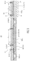
FIG. 2 illustrates anexemplary resistor 200.Exemplary resistor 200 may include n-well 202,P+ contact point 204, N+ contact point 206, p-sub area 208, stacked n-well resistor 210, stacked n-well resistor 212,contact A 214,contact C 216,depletion region 218 and p-sub 220. - In exemplary stacked n-well resistor 210 a n-well 202 may be in polysilicon substrate p-
sub area 208. Stacked n-well resistor 210 may have two contacts, 214 A and 216 C respectively. Contact A 214 may also be connected to the p-sub area 208. When a voltage is applied to contactC 216, a depletion region may be formed as indicated bydepletion region 218. Thedepletion region 218 effectively may make the n-well 202 less deep and thereby more highly resistive. The resistance may be dependent on the applied voltage over the resistor.P+ contact point 204 may connectcontact A 214 to p-sub area 208. Similarly, N+ contact point 206 may connectcontact A 214 to n-well 202. Stacked n-well resistor 212 may be similar to stacked n-well resistor 210. - In some embodiments, a stacked n-
well resistor 210 may include separate resistors on different substrates. P-sub 208 and p-sub 220 may be biased at the taps between the stacked n-well resistors -
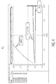
FIG. 3 includes a cross section of a poly resistor on n-well and a poly resistor on p-well that may be used in certain embodiments. The resistor structure may include twostacks stack 302 may have a poly resistor on n-well under the STI. The poly resistor on n-wells ofstack 302 may be biased at a positive voltage compared to the average voltage over the resistor stack. Theother stack 304 may have poly resistor on p-well under the STI. The poly resistor on p-wells understack 304 may be biased at a negative voltage compared to the average voltage over the resistor stack. -
FIG. 4 illustrates exemplary resistance values 400. Exemplary resistance values 400, demonstrates resistor values as a function of the applied voltage over the resistor for various resistors in the used IC technology. Exemplary resistance values 400 demonstrates that poly resistors tend to be the most linear resistors. The IC technology in which embodiments may be applied, include for example a 140nm CMOS process completed with high voltage high power transistors on a SiO2 isolated substrate (SOI). Some of the poly-resistors in this technology may be the most linear resistors available. - Two poly resistor structures may be available in the process such as n-well 302 and p-well 304. Both may be on top of a shallow trench isolator (STI) and thus are galvanic separated from the substrate/well below. Both resistors may have small voltage dependence.
- The maximum allowable voltage between the poly resistor and the well beneath may be 17V above which, there may be be voltage breakdown through an STI. A stack of three resistors may cope with the 40V input voltage of the converter, or output voltage of the digital amplifier. The three wells may be isolated from each other by applying sufficient lateral spacing in combination with deep trench isolation. By stacking three resistors in series the max allowable voltage may be tripled compared to a single resistor.
- In a simulated resistor test using three resistors in series, a Total Harmonic Distortion (THD) of -86dB was achieved, far below the desired 100dB. The used device models were confirmed to model non-linearity. Results were for a poly resistor on n-well alone such as
stack 302. Poly resistor on p-well, such asstack 304 performs the same. Further simulations demonstrated that 24 stacked resistors change the THD by only 4dB. More than 200 stacked resistors result in 100dB THD performance. - The stack of poly resistor on n-well resistors where the n-wells are biased by the voltage at the top of the individual resistors may have a small but not neglectable voltage coefficient. Each resistor in this stack may have a n-well potential which is positive compared to the average potential of the poly resistor itself. Vn-well-poly is positive. Through accumulation, such as for example more electrons in the poly, the resistance of the poly in the resistor may be reduced slightly. This reduction of the resistance may be dependent on Vn-well-poly and thus in the end may be dependent on the applied voltage over the stack. The poly resistor on n-well may have a negative voltage coefficient.
- For the poly resistor on p-well a similar effect may take place. The bias of the p-well may be chosen negative as compared to the average potential of the poly resistor on top. This may be done by connecting the p-well to the bottom of the individual resistors in the stack. Vp-well-poly may be negative, which may cause depletion, or fewer electrons in the poly which may result in an increase of the poly resistance. The poly resistor on p-well may have a positive voltage coefficient.
- Because both resistor types may be of the same poly-silicon, such as using the same doping, for example, and may be on the same STI layer, their voltage dependency may be equal except for the sign. A parallel circuit of two stacks of both types with the above described well biasing, may cancel the residual voltage dependency. The voltage coefficient may be equal to zero.
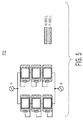
-
FIG. 5 illustrates an exemplary embodiment of a linearhigh voltage resistor 500. An embodiment of a linear high voltage resistor's structure may include: 2 resistors, or 2 strings of resistors in parallel. The number of resistors in each string may be one, two, three etc. In an exemplary embodiment of a linear high voltage resistor 500 a stack of three is used. Both strings may be made of poly resistors on top of STI with one string, for example, with poly resistor on n-well under the STI and the other string with poly resistor on p-well under the STI. The poly resistor on n-wells may be biased by the voltage on the top of the individual resistors. The poly resistor on p-well's may similarly be biased by the voltage at the bottom of the individual resistor. The result of a circuit simulation using compact models showed the change in THD, -100dB and -102dB was achieved. - This cancelling of the voltage coefficient was verified with measurements on existing silicon. In this silicon, there was access to both resistor terminals, as well the n-well or p-well beneath the resistor.
-
FIG. 6 illustrates measured resistance versus voltage for an embodiment of the linear highvoltage resistor graph 600.Graph 600 demonstrates the normalized resistance versus the applied voltage over the resistor both for measured data as well the result of circuit simulations using a compact model. Also in measurements the voltage dependency of both type resistors with the appropriate well-biasing may cancel each other. This cancelling may be proven for voltages over a single resistor up to 25V. TheGraph 600 also shows that the models are a bit too optimistic underlining the desire for some embodiments. - The resistors have some matching recommendations as well. The amplifier output voltage offset recommendation is Voffs <12.5mV (1□) when the DC output voltage is 7.2V.

- The □□R/R may be dependent on the active area of the resistor and some constants belonging to the particular IC-technology.
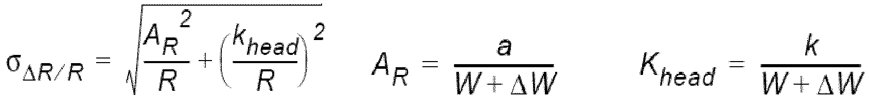
- Since the resistance may be a given, the W/L ratio may be fixed. The offset voltage may be expressed as a function of the Width of the resistor. A plot of this equation indicates a width of the resistor that is at least 10um to satisfy the offset recommendation. Some embodiments may use 11 um, 12um, 13um etc. With a structure of parallel resistor strings on top of apoly resistor on n-well and a poly resistor on p-well both strings may have a minium width of 5. The area of the complete solution may be dominated by the matching requirement. The extra spacing between the two resistor strings may only mildy increase the area for the complete resistor structure.
- Under a self-heating effect, a change in resistance due to the heating up of the resistor may be caused by dissipation in the resistor from the current through, and/or the voltage over the resistor. This may be due to the temperature coefficient of the resistor. Self heating may spoil the linearity of a resistor. The poly resistor may be thermally isolated from the bulk of the IC by the STI.
-
FIG. 7 illustrates an exemplary resistor using a first orderthermal model 700. A first order thermal model may be used to determinate the increase of temperature in the poly as result of dissipation in the poly. The temperature change, □□□□is defined as:

- The temperature rise may depend on W and L of resistor. An increase of the area of the resistor may reduce the self-heating effect. For example, if


- The resistors with, for example, W=12um, are already large enough not to suffer too much from the self heating effect.
- Although the various exemplary embodiments have been described in detail with particular reference to certain exemplary aspects thereof, it should be understood that the idea is capable of other embodiments and its details are capable of modifications in various obvious respects. As is readily apparent to those skilled in the art, variations and modifications can be affected while remaining within the spirit and scope of the embodiments. Accordingly, the foregoing disclosure, description, and figures are for illustrative purposes only and do not in any way limit the invention, which is defined only by the claims.
Claims (15)
- A resistor comprising:a poly resistor on n-well connected to a first shallow trench isolator; anda poly resistor on p-well connected in parallel to a second shallow trench isolator, wherein the poly resistor on n-well and poly resistor on p-well are biased oppositely.
- The resistor of claim 1, wherein the resistor creates a linear voltage output.
- The resistor of claim 1 wherein a resistor circuit is made up of three poly resistors on n-well connected in series in parallel with three poly resistors on p-well connected in series.
- The resistor of claim 1 wherein the resistor is made using a poly-Silicon substrate.
- The resistor of claim 1 wherein the resistor is used in an audio sigma delta conversion process.
- The resistor of claim 1 wherein the poly resistor on n-well is biased at a positive voltage compared to the voltage over the resistor and the poly resistor on p-well is biased at a negative voltage compared to the voltage over the resistor.
- The resistor of claim 1 wherein a resistor circuit is made up of two poly resistors on n-well connected in series in parallel with two poly resistors on p-well connected in series.
- The resistor of claim 1 wherein the resistor is connected to a low-latency analaog to digital converter.
- The resistor of claim 1 wherein the width of the resistor is at least 10um.
- The resistor of claim 1 wherein the poly resistor on n-well is biased at the top of the resistor, and the poly resistor on p-well is biased at the top of the resistor.
- An audio system comprising:an analog to digital converter (ADC);a resistor connected to the ADC comprising:a poly resistor on n-well connected to a first shallow trench isolator;a poly resistor on p-well connected in parallel to a second shallow trench isolator, wherein the poly resistor on n-well and poly resistor on p-well are biased oppositely; anda digital amplifier connected to the ADC.
- The audio system of claim 11, wherein the resistor creates a linear voltage output.
- An analaog to digital converter comprising:a low-latency analog to digital converter (LL-ADC), wherein the LL-ADC outputs current into a resistor comprising:a poly resistor on n-well connected to a first shallow trench isolator; anda poly resistor on p-well connected in parallel to a second shallow trench isolator, wherein the poly resistor on n-well and poly resistor on p-well are biased oppositely.
- The analaog to digital converter of claim 0 wherein the LL-ADC is configured using low voltage components.
- The analaog to digital converter of claim 0 wherein a resistor circuit is made up of three poly resistors on n-well connected in series in parallel with three poly resistors on p-well connected in series.
Applications Claiming Priority (1)
| Application Number | Priority Date | Filing Date | Title |
|---|---|---|---|
| US14/591,087 US9825028B2 (en) | 2015-01-07 | 2015-01-07 | Ultra linear high voltage resistors |
Publications (3)
| Publication Number | Publication Date |
|---|---|
| EP3043384A2 true EP3043384A2 (en) | 2016-07-13 |
| EP3043384A3 EP3043384A3 (en) | 2016-10-26 |
| EP3043384B1 EP3043384B1 (en) | 2024-11-06 |
Family
ID=55027415
Family Applications (1)
| Application Number | Title | Priority Date | Filing Date |
|---|---|---|---|
| EP15201893.3A Active EP3043384B1 (en) | 2015-01-07 | 2015-12-22 | Ultra linear high voltage resistors |
Country Status (2)
| Country | Link |
|---|---|
| US (1) | US9825028B2 (en) |
| EP (1) | EP3043384B1 (en) |
Families Citing this family (4)
| Publication number | Priority date | Publication date | Assignee | Title |
|---|---|---|---|---|
| EP3451398A1 (en) * | 2017-09-01 | 2019-03-06 | MediaTek Inc. | Impedance circuit with poly-resistor |
| JP7027176B2 (en) * | 2018-01-22 | 2022-03-01 | ラピスセミコンダクタ株式会社 | Semiconductor device |
| US10892771B1 (en) * | 2019-09-25 | 2021-01-12 | Texas Instruments Incorporated | Segmented resistor digital-to-analog converter |
| US12328883B2 (en) | 2022-06-07 | 2025-06-10 | Nxp Usa, Inc. | Polycrystalline semiconductor resistor |
Family Cites Families (16)
| Publication number | Priority date | Publication date | Assignee | Title |
|---|---|---|---|---|
| US4164668A (en) | 1977-05-12 | 1979-08-14 | International Business Machines Corporation | Method of correcting the voltage coefficient of resistors implanted or diffused in a semiconductor substrate |
| US6291306B1 (en) | 1999-07-19 | 2001-09-18 | Taiwan Semiconductor Manufacturing Company | Method of improving the voltage coefficient of resistance of high polysilicon resistors |
| JP2001320019A (en) * | 2000-05-08 | 2001-11-16 | Seiko Instruments Inc | Method for manufacturing semiconductor device |
| US20040070050A1 (en) * | 2002-10-10 | 2004-04-15 | Taiwan Semiconductor Manufacturing Company | Structures of vertical resistors and FETs as controlled by electrical field penetration and a band-gap voltage reference using vertical FETs operating in accumulation through the field penetration effect |
| US7498657B2 (en) * | 2002-10-10 | 2009-03-03 | Taiwan Semiconductor Manufacturing Co., Ltd. | Vertical resistors and band-gap voltage reference circuits |
| US6759729B1 (en) * | 2002-10-16 | 2004-07-06 | Newport Fab, Llc | Temperature insensitive resistor in an IC chip |
| US7242074B2 (en) * | 2004-12-06 | 2007-07-10 | Lsi Corporation | Reduced capacitance resistors |
| US7241663B2 (en) * | 2005-04-19 | 2007-07-10 | Texas Instruments Incorporated | Maskless multiple sheet polysilicon resistor |
| JP2010109233A (en) * | 2008-10-31 | 2010-05-13 | Renesas Technology Corp | Semiconductor device |
| KR101770585B1 (en) * | 2010-09-03 | 2017-08-24 | 삼성전자주식회사 | Resistor array and Semiconductor memory device including the same |
| JP2012119383A (en) | 2010-11-29 | 2012-06-21 | Renesas Electronics Corp | Semiconductor device and manufacturing method thereof |
| US20120292740A1 (en) * | 2011-05-19 | 2012-11-22 | Macronix International Co., Ltd. | High voltage resistance semiconductor device and method of manufacturing a high voltage resistance semiconductor device |
| US9373619B2 (en) * | 2011-08-01 | 2016-06-21 | Taiwan Semiconductor Manufacturing Company, Ltd. | High voltage resistor with high voltage junction termination |
| US8624322B1 (en) * | 2012-07-17 | 2014-01-07 | Taiwan Semiconductor Manufacturing Company, Ltd. | High voltage device with a parallel resistor |
| US8716827B2 (en) | 2012-09-11 | 2014-05-06 | Texas Instruments Incorporated | Diffusion resistor with reduced voltage coefficient of resistance and increased breakdown voltage using CMOS wells |
| US9602126B2 (en) * | 2012-12-21 | 2017-03-21 | Teledyne Dalsa B.V. | Sigma-delta analog-to-digital converter |
-
2015
- 2015-01-07 US US14/591,087 patent/US9825028B2/en active Active
- 2015-12-22 EP EP15201893.3A patent/EP3043384B1/en active Active
Also Published As
| Publication number | Publication date |
|---|---|
| EP3043384A3 (en) | 2016-10-26 |
| US20160197592A1 (en) | 2016-07-07 |
| US9825028B2 (en) | 2017-11-21 |
| EP3043384B1 (en) | 2024-11-06 |
Similar Documents
| Publication | Publication Date | Title |
|---|---|---|
| US10658987B2 (en) | Amplifier circuit for cryogenic applications | |
| CN102084489B (en) | Dynamically-driven deep N-well circuit | |
| EP3043384B1 (en) | Ultra linear high voltage resistors | |
| US7724077B2 (en) | Stacked cascode current source | |
| US20220390493A1 (en) | Power Detector with Wide Dynamic Range | |
| US10535651B2 (en) | Impedance circuit with poly-resistor | |
| US10510823B2 (en) | Impedance circuit with poly-resistor | |
| US8482099B2 (en) | Poly-resistor, and linear amplifier | |
| Huijsing | Instrumentation amplifiers: A comparative study on behalf of monolithic integration | |
| US11948967B2 (en) | Polysilicon resistor | |
| JP5454366B2 (en) | Power amplifier module and portable information terminal | |
| US8686744B2 (en) | Precision measurement of capacitor mismatch | |
| US7705678B2 (en) | Amplifier using impedance circuit for canceling cutoff | |
| US8723294B2 (en) | Resistance element and inverting buffer circuit | |
| US10461702B2 (en) | Amplifier circuit having poly resistor with biased depletion region | |
| JP2013197487A (en) | Inverting buffer circuit and electronic volume circuit | |
| US20060119430A1 (en) | Adaptive bias scheme for high-voltage compliance in serial links | |
| JP2006078204A (en) | Current detection circuit | |
| JP2013207217A (en) | Non-inverting buffer circuit | |
| JP7074398B2 (en) | Voltage amplifier circuit device and voltage application circuit | |
| JP5420230B2 (en) | Overvoltage protection element | |
| Chava | A low input-current chopper amplifier | |
| Yeom | Temperature Compensated, High Common Mode Range, Cu-Trace Based Current Shunt Monitors Design and Analysis | |
| CN111418061A (en) | Single capacitor used as RC filter | |
| JP2014212475A (en) | Semiconductor integrated circuit device |
Legal Events
| Date | Code | Title | Description |
|---|---|---|---|
| PUAI | Public reference made under article 153(3) epc to a published international application that has entered the european phase |
Free format text: ORIGINAL CODE: 0009012 |
|
| AK | Designated contracting states |
Kind code of ref document: A2 Designated state(s): AL AT BE BG CH CY CZ DE DK EE ES FI FR GB GR HR HU IE IS IT LI LT LU LV MC MK MT NL NO PL PT RO RS SE SI SK SM TR |
|
| AX | Request for extension of the european patent |
Extension state: BA ME |
|
| PUAL | Search report despatched |
Free format text: ORIGINAL CODE: 0009013 |
|
| AK | Designated contracting states |
Kind code of ref document: A3 Designated state(s): AL AT BE BG CH CY CZ DE DK EE ES FI FR GB GR HR HU IE IS IT LI LT LU LV MC MK MT NL NO PL PT RO RS SE SI SK SM TR |
|
| AX | Request for extension of the european patent |
Extension state: BA ME |
|
| RIC1 | Information provided on ipc code assigned before grant |
Ipc: H01L 27/08 20060101AFI20160922BHEP Ipc: H01L 49/02 20060101ALI20160922BHEP |
|
| 17P | Request for examination filed |
Effective date: 20170426 |
|
| RBV | Designated contracting states (corrected) |
Designated state(s): AL AT BE BG CH CY CZ DE DK EE ES FI FR GB GR HR HU IE IS IT LI LT LU LV MC MK MT NL NO PL PT RO RS SE SI SK SM TR |
|
| STAA | Information on the status of an ep patent application or granted ep patent |
Free format text: STATUS: THE APPLICATION HAS BEEN PUBLISHED |
|
| STAA | Information on the status of an ep patent application or granted ep patent |
Free format text: STATUS: REQUEST FOR EXAMINATION WAS MADE |
|
| STAA | Information on the status of an ep patent application or granted ep patent |
Free format text: STATUS: EXAMINATION IS IN PROGRESS |
|
| 17Q | First examination report despatched |
Effective date: 20190423 |
|
| GRAP | Despatch of communication of intention to grant a patent |
Free format text: ORIGINAL CODE: EPIDOSNIGR1 |
|
| STAA | Information on the status of an ep patent application or granted ep patent |
Free format text: STATUS: GRANT OF PATENT IS INTENDED |
|
| RIC1 | Information provided on ipc code assigned before grant |
Ipc: H03M 1/12 20060101ALN20240516BHEP Ipc: H03F 3/217 20060101ALI20240516BHEP Ipc: H10N 97/00 20230101ALI20240516BHEP Ipc: H01L 27/08 20060101AFI20240516BHEP |
|
| INTG | Intention to grant announced |
Effective date: 20240607 |
|
| RIC1 | Information provided on ipc code assigned before grant |
Ipc: H03M 1/12 20060101ALN20240524BHEP Ipc: H03F 3/217 20060101ALI20240524BHEP Ipc: H10N 97/00 20230101ALI20240524BHEP Ipc: H01L 27/08 20060101AFI20240524BHEP |
|
| RIN1 | Information on inventor provided before grant (corrected) |
Inventor name: VAN LERSEL, HENDRIKUS Inventor name: KOERTS, MATTHEUS JOHAN |
|
| GRAS | Grant fee paid |
Free format text: ORIGINAL CODE: EPIDOSNIGR3 |
|
| GRAA | (expected) grant |
Free format text: ORIGINAL CODE: 0009210 |
|
| STAA | Information on the status of an ep patent application or granted ep patent |
Free format text: STATUS: THE PATENT HAS BEEN GRANTED |
|
| AK | Designated contracting states |
Kind code of ref document: B1 Designated state(s): AL AT BE BG CH CY CZ DE DK EE ES FI FR GB GR HR HU IE IS IT LI LT LU LV MC MK MT NL NO PL PT RO RS SE SI SK SM TR |
|
| REG | Reference to a national code |
Ref country code: GB Ref legal event code: FG4D |
|
| REG | Reference to a national code |
Ref country code: CH Ref legal event code: EP |
|
| REG | Reference to a national code |
Ref country code: DE Ref legal event code: R096 Ref document number: 602015090314 Country of ref document: DE |
|
| REG | Reference to a national code |
Ref country code: DE Ref legal event code: R079 Ref document number: 602015090314 Country of ref document: DE Free format text: PREVIOUS MAIN CLASS: H01L0027080000 Ipc: H10D0001000000 |
|
| REG | Reference to a national code |
Ref country code: IE Ref legal event code: FG4D |
|
| REG | Reference to a national code |
Ref country code: LT Ref legal event code: MG9D |
|
| REG | Reference to a national code |
Ref country code: NL Ref legal event code: MP Effective date: 20241106 |
|
| PG25 | Lapsed in a contracting state [announced via postgrant information from national office to epo] |
Ref country code: HR Free format text: LAPSE BECAUSE OF FAILURE TO SUBMIT A TRANSLATION OF THE DESCRIPTION OR TO PAY THE FEE WITHIN THE PRESCRIBED TIME-LIMIT Effective date: 20241106 Ref country code: IS Free format text: LAPSE BECAUSE OF FAILURE TO SUBMIT A TRANSLATION OF THE DESCRIPTION OR TO PAY THE FEE WITHIN THE PRESCRIBED TIME-LIMIT Effective date: 20250306 Ref country code: PT Free format text: LAPSE BECAUSE OF FAILURE TO SUBMIT A TRANSLATION OF THE DESCRIPTION OR TO PAY THE FEE WITHIN THE PRESCRIBED TIME-LIMIT Effective date: 20250306 |
|
| PG25 | Lapsed in a contracting state [announced via postgrant information from national office to epo] |
Ref country code: FI Free format text: LAPSE BECAUSE OF FAILURE TO SUBMIT A TRANSLATION OF THE DESCRIPTION OR TO PAY THE FEE WITHIN THE PRESCRIBED TIME-LIMIT Effective date: 20241106 Ref country code: NL Free format text: LAPSE BECAUSE OF FAILURE TO SUBMIT A TRANSLATION OF THE DESCRIPTION OR TO PAY THE FEE WITHIN THE PRESCRIBED TIME-LIMIT Effective date: 20241106 |
|
| REG | Reference to a national code |
Ref country code: AT Ref legal event code: MK05 Ref document number: 1740376 Country of ref document: AT Kind code of ref document: T Effective date: 20241106 |
|
| PG25 | Lapsed in a contracting state [announced via postgrant information from national office to epo] |
Ref country code: BG Free format text: LAPSE BECAUSE OF FAILURE TO SUBMIT A TRANSLATION OF THE DESCRIPTION OR TO PAY THE FEE WITHIN THE PRESCRIBED TIME-LIMIT Effective date: 20241106 |
|
| PG25 | Lapsed in a contracting state [announced via postgrant information from national office to epo] |
Ref country code: ES Free format text: LAPSE BECAUSE OF FAILURE TO SUBMIT A TRANSLATION OF THE DESCRIPTION OR TO PAY THE FEE WITHIN THE PRESCRIBED TIME-LIMIT Effective date: 20241106 |
|
| PG25 | Lapsed in a contracting state [announced via postgrant information from national office to epo] |
Ref country code: NO Free format text: LAPSE BECAUSE OF FAILURE TO SUBMIT A TRANSLATION OF THE DESCRIPTION OR TO PAY THE FEE WITHIN THE PRESCRIBED TIME-LIMIT Effective date: 20250206 |
|
| PG25 | Lapsed in a contracting state [announced via postgrant information from national office to epo] |
Ref country code: LV Free format text: LAPSE BECAUSE OF FAILURE TO SUBMIT A TRANSLATION OF THE DESCRIPTION OR TO PAY THE FEE WITHIN THE PRESCRIBED TIME-LIMIT Effective date: 20241106 Ref country code: GR Free format text: LAPSE BECAUSE OF FAILURE TO SUBMIT A TRANSLATION OF THE DESCRIPTION OR TO PAY THE FEE WITHIN THE PRESCRIBED TIME-LIMIT Effective date: 20250207 Ref country code: AT Free format text: LAPSE BECAUSE OF FAILURE TO SUBMIT A TRANSLATION OF THE DESCRIPTION OR TO PAY THE FEE WITHIN THE PRESCRIBED TIME-LIMIT Effective date: 20241106 |
|
| PG25 | Lapsed in a contracting state [announced via postgrant information from national office to epo] |
Ref country code: PL Free format text: LAPSE BECAUSE OF FAILURE TO SUBMIT A TRANSLATION OF THE DESCRIPTION OR TO PAY THE FEE WITHIN THE PRESCRIBED TIME-LIMIT Effective date: 20241106 |
|
| PG25 | Lapsed in a contracting state [announced via postgrant information from national office to epo] |
Ref country code: RS Free format text: LAPSE BECAUSE OF FAILURE TO SUBMIT A TRANSLATION OF THE DESCRIPTION OR TO PAY THE FEE WITHIN THE PRESCRIBED TIME-LIMIT Effective date: 20250206 |
|
| PG25 | Lapsed in a contracting state [announced via postgrant information from national office to epo] |
Ref country code: SM Free format text: LAPSE BECAUSE OF FAILURE TO SUBMIT A TRANSLATION OF THE DESCRIPTION OR TO PAY THE FEE WITHIN THE PRESCRIBED TIME-LIMIT Effective date: 20241106 |
|
| PG25 | Lapsed in a contracting state [announced via postgrant information from national office to epo] |
Ref country code: DK Free format text: LAPSE BECAUSE OF FAILURE TO SUBMIT A TRANSLATION OF THE DESCRIPTION OR TO PAY THE FEE WITHIN THE PRESCRIBED TIME-LIMIT Effective date: 20241106 |
|
| PG25 | Lapsed in a contracting state [announced via postgrant information from national office to epo] |
Ref country code: EE Free format text: LAPSE BECAUSE OF FAILURE TO SUBMIT A TRANSLATION OF THE DESCRIPTION OR TO PAY THE FEE WITHIN THE PRESCRIBED TIME-LIMIT Effective date: 20241106 |
|
| PG25 | Lapsed in a contracting state [announced via postgrant information from national office to epo] |
Ref country code: RO Free format text: LAPSE BECAUSE OF FAILURE TO SUBMIT A TRANSLATION OF THE DESCRIPTION OR TO PAY THE FEE WITHIN THE PRESCRIBED TIME-LIMIT Effective date: 20241106 |
|
| PG25 | Lapsed in a contracting state [announced via postgrant information from national office to epo] |
Ref country code: SK Free format text: LAPSE BECAUSE OF FAILURE TO SUBMIT A TRANSLATION OF THE DESCRIPTION OR TO PAY THE FEE WITHIN THE PRESCRIBED TIME-LIMIT Effective date: 20241106 |
|
| PG25 | Lapsed in a contracting state [announced via postgrant information from national office to epo] |
Ref country code: CZ Free format text: LAPSE BECAUSE OF FAILURE TO SUBMIT A TRANSLATION OF THE DESCRIPTION OR TO PAY THE FEE WITHIN THE PRESCRIBED TIME-LIMIT Effective date: 20241106 |
|
| PG25 | Lapsed in a contracting state [announced via postgrant information from national office to epo] |
Ref country code: IT Free format text: LAPSE BECAUSE OF FAILURE TO SUBMIT A TRANSLATION OF THE DESCRIPTION OR TO PAY THE FEE WITHIN THE PRESCRIBED TIME-LIMIT Effective date: 20241106 |
|
| P01 | Opt-out of the competence of the unified patent court (upc) registered |
Free format text: CASE NUMBER: APP_29782/2025 Effective date: 20250623 |
|
| REG | Reference to a national code |
Ref country code: CH Ref legal event code: PL |
|
| REG | Reference to a national code |
Ref country code: DE Ref legal event code: R097 Ref document number: 602015090314 Country of ref document: DE |
|
| PG25 | Lapsed in a contracting state [announced via postgrant information from national office to epo] |
Ref country code: LU Free format text: LAPSE BECAUSE OF NON-PAYMENT OF DUE FEES Effective date: 20241222 |
|
| PG25 | Lapsed in a contracting state [announced via postgrant information from national office to epo] |
Ref country code: SE Free format text: LAPSE BECAUSE OF FAILURE TO SUBMIT A TRANSLATION OF THE DESCRIPTION OR TO PAY THE FEE WITHIN THE PRESCRIBED TIME-LIMIT Effective date: 20241106 |
|
| PLBE | No opposition filed within time limit |
Free format text: ORIGINAL CODE: 0009261 |
|
| STAA | Information on the status of an ep patent application or granted ep patent |
Free format text: STATUS: NO OPPOSITION FILED WITHIN TIME LIMIT |
|
| PG25 | Lapsed in a contracting state [announced via postgrant information from national office to epo] |
Ref country code: MC Free format text: LAPSE BECAUSE OF FAILURE TO SUBMIT A TRANSLATION OF THE DESCRIPTION OR TO PAY THE FEE WITHIN THE PRESCRIBED TIME-LIMIT Effective date: 20241106 |
|
| REG | Reference to a national code |
Ref country code: BE Ref legal event code: MM Effective date: 20241231 |
|
| 26N | No opposition filed |
Effective date: 20250807 |
|
| PG25 | Lapsed in a contracting state [announced via postgrant information from national office to epo] |
Ref country code: BE Free format text: LAPSE BECAUSE OF NON-PAYMENT OF DUE FEES Effective date: 20241231 |
|
| PG25 | Lapsed in a contracting state [announced via postgrant information from national office to epo] |
Ref country code: CH Free format text: LAPSE BECAUSE OF NON-PAYMENT OF DUE FEES Effective date: 20241231 |
|
| PG25 | Lapsed in a contracting state [announced via postgrant information from national office to epo] |
Ref country code: IE Free format text: LAPSE BECAUSE OF NON-PAYMENT OF DUE FEES Effective date: 20241222 |
|
| GBPC | Gb: european patent ceased through non-payment of renewal fee |
Effective date: 20250206 |
|
| PGFP | Annual fee paid to national office [announced via postgrant information from national office to epo] |
Ref country code: DE Payment date: 20251126 Year of fee payment: 11 |
|
| PG25 | Lapsed in a contracting state [announced via postgrant information from national office to epo] |
Ref country code: GB Free format text: LAPSE BECAUSE OF NON-PAYMENT OF DUE FEES Effective date: 20250206 |
|
| PGFP | Annual fee paid to national office [announced via postgrant information from national office to epo] |
Ref country code: FR Payment date: 20251119 Year of fee payment: 11 |