EP3043382A1 - Circuit board assembly with high and low frequency substrates - Google Patents
Circuit board assembly with high and low frequency substrates Download PDFInfo
- Publication number
- EP3043382A1 EP3043382A1 EP15200529.4A EP15200529A EP3043382A1 EP 3043382 A1 EP3043382 A1 EP 3043382A1 EP 15200529 A EP15200529 A EP 15200529A EP 3043382 A1 EP3043382 A1 EP 3043382A1
- Authority
- EP
- European Patent Office
- Prior art keywords
- substrate
- mmic
- frequency signal
- radio
- frequency
- Prior art date
- Legal status (The legal status is an assumption and is not a legal conclusion. Google has not performed a legal analysis and makes no representation as to the accuracy of the status listed.)
- Granted
Links
Images


Classifications
-
- H—ELECTRICITY
- H05—ELECTRIC TECHNIQUES NOT OTHERWISE PROVIDED FOR
- H05K—PRINTED CIRCUITS; CASINGS OR CONSTRUCTIONAL DETAILS OF ELECTRIC APPARATUS; MANUFACTURE OF ASSEMBLAGES OF ELECTRICAL COMPONENTS
- H05K1/00—Printed circuits
- H05K1/02—Details
- H05K1/14—Structural association of two or more printed circuits
- H05K1/141—One or more single auxiliary printed circuits mounted on a main printed circuit, e.g. modules, adapters
-
- H—ELECTRICITY
- H01—ELECTRIC ELEMENTS
- H01Q—ANTENNAS, i.e. RADIO AERIALS
- H01Q1/00—Details of, or arrangements associated with, antennas
- H01Q1/50—Structural association of antennas with earthing switches, lead-in devices or lightning protectors
-
- H—ELECTRICITY
- H01—ELECTRIC ELEMENTS
- H01Q—ANTENNAS, i.e. RADIO AERIALS
- H01Q1/00—Details of, or arrangements associated with, antennas
- H01Q1/12—Supports; Mounting means
- H01Q1/22—Supports; Mounting means by structural association with other equipment or articles
- H01Q1/225—Supports; Mounting means by structural association with other equipment or articles used in level-measurement devices, e.g. for level gauge measurement
-
- H—ELECTRICITY
- H01—ELECTRIC ELEMENTS
- H01Q—ANTENNAS, i.e. RADIO AERIALS
- H01Q21/00—Antenna arrays or systems
- H01Q21/06—Arrays of individually energised antenna units similarly polarised and spaced apart
- H01Q21/061—Two dimensional planar arrays
- H01Q21/065—Patch antenna array
-
- H—ELECTRICITY
- H05—ELECTRIC TECHNIQUES NOT OTHERWISE PROVIDED FOR
- H05K—PRINTED CIRCUITS; CASINGS OR CONSTRUCTIONAL DETAILS OF ELECTRIC APPARATUS; MANUFACTURE OF ASSEMBLAGES OF ELECTRICAL COMPONENTS
- H05K1/00—Printed circuits
- H05K1/02—Details
-
- H—ELECTRICITY
- H05—ELECTRIC TECHNIQUES NOT OTHERWISE PROVIDED FOR
- H05K—PRINTED CIRCUITS; CASINGS OR CONSTRUCTIONAL DETAILS OF ELECTRIC APPARATUS; MANUFACTURE OF ASSEMBLAGES OF ELECTRICAL COMPONENTS
- H05K1/00—Printed circuits
- H05K1/02—Details
- H05K1/0213—Electrical arrangements not otherwise provided for
- H05K1/0237—High frequency adaptations
- H05K1/0243—Printed circuits associated with mounted high frequency components
-
- H—ELECTRICITY
- H10—SEMICONDUCTOR DEVICES; ELECTRIC SOLID-STATE DEVICES NOT OTHERWISE PROVIDED FOR
- H10W—GENERIC PACKAGES, INTERCONNECTIONS, CONNECTORS OR OTHER CONSTRUCTIONAL DETAILS OF DEVICES COVERED BY CLASS H10
- H10W44/00—Electrical arrangements for controlling or matching impedance
- H10W44/20—Electrical arrangements for controlling or matching impedance at high-frequency [HF] or radio frequency [RF]
-
- H—ELECTRICITY
- H01—ELECTRIC ELEMENTS
- H01P—WAVEGUIDES; RESONATORS, LINES, OR OTHER DEVICES OF THE WAVEGUIDE TYPE
- H01P5/00—Coupling devices of the waveguide type
- H01P5/02—Coupling devices of the waveguide type with invariable factor of coupling
- H01P5/022—Transitions between lines of the same kind and shape, but with different dimensions
- H01P5/028—Transitions between lines of the same kind and shape, but with different dimensions between strip lines
-
- H—ELECTRICITY
- H05—ELECTRIC TECHNIQUES NOT OTHERWISE PROVIDED FOR
- H05K—PRINTED CIRCUITS; CASINGS OR CONSTRUCTIONAL DETAILS OF ELECTRIC APPARATUS; MANUFACTURE OF ASSEMBLAGES OF ELECTRICAL COMPONENTS
- H05K1/00—Printed circuits
- H05K1/18—Printed circuits structurally associated with non-printed electric components
- H05K1/182—Printed circuits structurally associated with non-printed electric components associated with components mounted in printed circuit boards [PCB], e.g. insert-mounted components [IMC]
- H05K1/184—Printed circuits structurally associated with non-printed electric components associated with components mounted in printed circuit boards [PCB], e.g. insert-mounted components [IMC] associated with components inserted in holes through the PCBs and wherein terminals of the components are connected to printed contacts on the walls of the holes or at the edges thereof or protruding over or into the holes
-
- H—ELECTRICITY
- H05—ELECTRIC TECHNIQUES NOT OTHERWISE PROVIDED FOR
- H05K—PRINTED CIRCUITS; CASINGS OR CONSTRUCTIONAL DETAILS OF ELECTRIC APPARATUS; MANUFACTURE OF ASSEMBLAGES OF ELECTRICAL COMPONENTS
- H05K2201/00—Indexing scheme relating to printed circuits covered by H05K1/00
- H05K2201/04—Assemblies of printed circuits
- H05K2201/041—Stacked PCBs, i.e. having neither an empty space nor mounted components in between
-
- H—ELECTRICITY
- H05—ELECTRIC TECHNIQUES NOT OTHERWISE PROVIDED FOR
- H05K—PRINTED CIRCUITS; CASINGS OR CONSTRUCTIONAL DETAILS OF ELECTRIC APPARATUS; MANUFACTURE OF ASSEMBLAGES OF ELECTRICAL COMPONENTS
- H05K2201/00—Indexing scheme relating to printed circuits covered by H05K1/00
- H05K2201/10—Details of components or other objects attached to or integrated in a printed circuit board
- H05K2201/10007—Types of components
-
- H—ELECTRICITY
- H05—ELECTRIC TECHNIQUES NOT OTHERWISE PROVIDED FOR
- H05K—PRINTED CIRCUITS; CASINGS OR CONSTRUCTIONAL DETAILS OF ELECTRIC APPARATUS; MANUFACTURE OF ASSEMBLAGES OF ELECTRICAL COMPONENTS
- H05K2201/00—Indexing scheme relating to printed circuits covered by H05K1/00
- H05K2201/10—Details of components or other objects attached to or integrated in a printed circuit board
- H05K2201/10007—Types of components
- H05K2201/10098—Components for radio transmission, e.g. radio frequency identification [RFID] tag, printed or non-printed antennas
-
- H—ELECTRICITY
- H05—ELECTRIC TECHNIQUES NOT OTHERWISE PROVIDED FOR
- H05K—PRINTED CIRCUITS; CASINGS OR CONSTRUCTIONAL DETAILS OF ELECTRIC APPARATUS; MANUFACTURE OF ASSEMBLAGES OF ELECTRICAL COMPONENTS
- H05K2203/00—Indexing scheme relating to apparatus or processes for manufacturing printed circuits covered by H05K3/00
- H05K2203/04—Soldering or other types of metallurgic bonding
- H05K2203/049—Wire bonding
-
- H—ELECTRICITY
- H05—ELECTRIC TECHNIQUES NOT OTHERWISE PROVIDED FOR
- H05K—PRINTED CIRCUITS; CASINGS OR CONSTRUCTIONAL DETAILS OF ELECTRIC APPARATUS; MANUFACTURE OF ASSEMBLAGES OF ELECTRICAL COMPONENTS
- H05K3/00—Apparatus or processes for manufacturing printed circuits
- H05K3/36—Assembling printed circuits with other printed circuits
- H05K3/368—Assembling printed circuits with other printed circuits parallel to each other
-
- H—ELECTRICITY
- H10—SEMICONDUCTOR DEVICES; ELECTRIC SOLID-STATE DEVICES NOT OTHERWISE PROVIDED FOR
- H10W—GENERIC PACKAGES, INTERCONNECTIONS, CONNECTORS OR OTHER CONSTRUCTIONAL DETAILS OF DEVICES COVERED BY CLASS H10
- H10W44/00—Electrical arrangements for controlling or matching impedance
- H10W44/20—Electrical arrangements for controlling or matching impedance at high-frequency [HF] or radio frequency [RF]
- H10W44/251—Electrical arrangements for controlling or matching impedance at high-frequency [HF] or radio frequency [RF] for monolithic microwave integrated circuits [MMIC]
-
- H—ELECTRICITY
- H10—SEMICONDUCTOR DEVICES; ELECTRIC SOLID-STATE DEVICES NOT OTHERWISE PROVIDED FOR
- H10W—GENERIC PACKAGES, INTERCONNECTIONS, CONNECTORS OR OTHER CONSTRUCTIONAL DETAILS OF DEVICES COVERED BY CLASS H10
- H10W72/00—Interconnections or connectors in packages
- H10W72/50—Bond wires
- H10W72/531—Shapes of wire connectors
- H10W72/5363—Shapes of wire connectors the connected ends being wedge-shaped
-
- H—ELECTRICITY
- H10—SEMICONDUCTOR DEVICES; ELECTRIC SOLID-STATE DEVICES NOT OTHERWISE PROVIDED FOR
- H10W—GENERIC PACKAGES, INTERCONNECTIONS, CONNECTORS OR OTHER CONSTRUCTIONAL DETAILS OF DEVICES COVERED BY CLASS H10
- H10W72/00—Interconnections or connectors in packages
- H10W72/50—Bond wires
- H10W72/541—Dispositions of bond wires
- H10W72/5445—Dispositions of bond wires being orthogonal to a side surface of the chip, e.g. parallel arrangements
Definitions
- This disclosure generally relates to a circuit board assembly, and more particularly relates to a cost efficient interconnection of substrates, electrical devices, and an antenna for transmitting and/or receiving a radio-frequency signal.
- MMIC Monolithic Microwave Integrated Circuit
- Standard packages such as a Quad Flat No-leads (QFN) package are not preferred for mm-wave devices as such packages do not provide suitable performance for quality RF interfaces.
- High-frequency substrates are generally more expensive than low-frequency (e.g. FR-4) substrates, so building an entire circuit board assembly using only a high-frequency substrate undesirably increases cost.
- a packaging solution for a MMIC requires efficient transfer of radio-frequency (RF) signals via a suitable substrate interface; as well as necessary low frequency signals for power, control signals, and baseband interfaces.
- RF radio-frequency
- a circuit board assembly includes a low-frequency (LF) substrate, a monolithic microwave integrated circuit (MMIC), a plurality of electrical components, a high-frequency (HF) substrate, a plurality of wire bonds, and an antenna.
- the LF substrate is formed of FR-4 type material.
- the LF substrate defines a top-side, a bottom-side, and a waveguide through the LF substrate configured to guide a radio-frequency signal from the top-side to the bottom-side.
- the MMIC is attached to the top-side and configured to output the radio-frequency signal.
- the plurality of electrical components are electrically attached to the LF substrate and configured to process a low-frequency signal.
- the HF substrate is attached to the top-side.
- the HF substrate is configured to define a solder pad configured to couple the low-frequency signal from the LF substrate to the HF substrate.
- the HF substrate is also configured to an opening through the HF substrate configured to surround the MMIC.
- the HF substrate is also configured to a vertical transition configured to guide the radio-frequency signal output by the MMIC to the waveguide.
- the plurality of wire bonds electrically connects the MMIC to the HF substrate and couple the radio-frequency signal from the MMIC to the vertical transition.
- the antenna is attached to the LF substrate and configured to radiate the radio-frequency signal from the waveguide.
- circuit board assembly that provides an economical assembly for electrical systems that have or process both relatively low-frequency signals with frequency spectrums less than 100MHz, including DC power, and relatively high frequency signals, i.e. radio-frequency signals with frequency spectrums greater than 1GHz.
- the circuit board assembly described herein would be well suited for an automotive radar system operating with a radar signal frequency of 76.5GHz. While the description presented herein is generally directed to the transmission of a radio-frequency signal, it is recognized that the teachings are applicable to circuit board assemblies that only receive a radio-frequency signal, and both transmit and receive a radio-frequency signal as would be the case for a radar system.
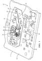
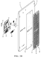
- Figs. 1 , 2A , 2B , and 2C cooperatively illustrate a non-limiting example of a circuit board assembly, hereafter referred to as the assembly 10.
- the assembly 10 is generally built upon or around a low-frequency substrate, hereafter the LF substrate 12.
- the LF substrate 12 is advantageously formed of FR-4 type material as it is relatively low in cost and readily available.
- the LF substrate defines a top-side 14, a bottom-side 16, and a waveguide 18 through the LF substrate 12 configured to guide a radio-frequency signal 20 ( Fig. 2A ) from the top-side 14 to the bottom-side 16.
- the waveguide 18 may be plated in a manner similar to a plated through-hole in order to better conduct or propagate the radio-frequency signal 20 through the LF substrate.
- the assembly 10 includes a monolithic microwave integrated circuit, hereafter the MMIC 22, attached to the top-side 14 and configured to output the radio-frequency signal 20. Additional features described below conduct or propagate the radio-frequency signal 20 from the MMIC 22 to the waveguide 18.
- the LF substrate 12 may be configured to include a heat sink 24 proximate to (e.g. underneath) the MMIC 22 to better dissipate heat emitted by the MMIC 22.
- the heat sink 24 may include an one or more vias or plated through-holes in the LF substrate 12, and/or one or layers of conductor such as copper foil that cooperate to spread and/or conduct heat away from the MMIC 22.
- the MMIC 22 may be attached to the LF substrate 12 by solder or an adhesive 32. If the heat sink 24 is needed, the adhesive 32 may be, for example, a thermally conductive epoxy.
- the assembly 10 includes a plurality of electrical components 26 electrically attached to the LF substrate 12.
- the electrical components 26 are configured to route, conduct, and/or process a low-frequency signal 28.
- the electrical components may include a capacitor, a resistor, or a processor such as a microprocessor.
- the low-frequency signal 28 is generally less than 100MHz because the FR-4 material used to form the LF substrate 12 is not well suited to higher frequency signals such as the radio-frequency signal 20.
- the assembly 10 includes a high-frequency substrate, hereafter the HF substrate 30 attached to the top-side 14 of the LF substrate 12.
- a suitable material for the HF substrate 30 is 0.5mm thick RO5880 manufactured by Rogers Corp.
- the HF substrate 30 is configured to define a solder pad 34 ( Fig. 2B ) used to couple the low-frequency signal 28 from a corresponding solder pad 36 ( Fig. 2A ) on the LF substrate 12 to the HF substrate 30.
- the MMIC 22 can be supplied with DC power and control signals from the lower cost FR-4 substrate, i.e. the LF substrate 12.
- the HF substrate 30 may include or define an opening 38 through the HF substrate 30 that surrounds the MMIC 22.
- a plurality of wire bonds 40 can then be used to electrically connect the MMIC 22 to the HF substrate 30 and thereby couple the radio-frequency signal 20 from the MMIC 22 to a microstrip 42 on the HF substrate 30.
- the length of the wire bonds 40 can be minimized which is advantageous for high frequency signals such as the radio-frequency signal 20.
- the thicknesses of the various parts that make up the assembly 10 are such that wire bond pads on the MMIC 22 are co-planar, or as close to co-planar as feasible, with wire bond pads on the HF substrate 30 so the length of the wire bonds 40 is minimized.
- the HF substrate 30 may include or define a vertical transition 44 configured to guide the radio-frequency signal 20 output by the MMIC 22 to the waveguide 18.
- the vertical transition 44 redirects the radio-frequency signal 20 propagating horizontally across the surface of the HF substrate 30 to propagate in a vertical direction through the waveguide 18 and to an antenna 46 attached to the bottom side 16 of the LF substrate 12.
- the antenna 46 is configured to radiate the radio-frequency signal 20 from the waveguide 18. While the explanation thus far has been directed to the radio-frequency signal 20 being output by the MMIC 22 and radiated by the antenna 46, it is contemplated that signals may be received by the antenna 46 and detected by the MMIC, as would be the case for a radar system using the assembly 10 described herein.
- solder pad 34 of the HF substrate 30, the solder pad 36 of the LF substrate 12, and solder material 48 cooperate to form a solder joint 50 to attached the HF substrate 30 to the LF substrate 12 and thereby provide a means to couple the low-frequency signal 28 between the HF substrate 30 to the LF substrate 12.
- the solder joint 50 has a thickness selected to optimize coupling of the radio-frequency signal 20 between the vertical transition 44 and the waveguide 18, but still provide adequate strength. In general, the thinner the solder joint 50, the better the coupling of the radio-frequency signal 20. However, if the solder joint 50 is too thin, the solder joint may have poor reliability.
- a suitable thickness of the solder material 48 after reflow is fifty micrometers (50um).
- the antenna 46 may include a support substrate 52 attached to the bottom-side 16 by an adhesive 54. If the operating frequency of the antenna 46 is 76.5 GHz, the support substrate 52 may be a 0.38 millimeter (mm) thick PTFE substrate. Elements 56 of the antenna 46 may have a patch size of 1.07mm square and a patch pitch of 2.98mm.
- a suitable material for the adhesive 54 is a silicone based adhesive with a suitable thickness of fifty micrometers (50um).
- a circuit board assembly (the assembly 10) suitable for applications such as an automotive radar system is provided.
- the assembly 10 uses a small RF substrate (the HF substrate 30) suitable for surface mount attachment to the LF substrate 12.
- the low frequency signal 28 interconnects through attachment of the substrates by the solder joint 50.
- Enhanced RF performance of the transition from the HF substrate 30 to the LF substrate is provided by a low profile solder connect that is relatively low when compared to typical BGA package techniques.
- the assembly 10 enables MMIC packaging with low and high frequency interconnects to generic FR4 substrate which is generally not suitable for efficient high frequency microstrip/stripline routing.
- the assembly 10 described herein is particularly useful as commercial products are increasingly using Monolithic Microwave Integrated Circuits (MMICs) to support mm-wave products that require both low and high frequency RF interfaces.
- MMICs Monolithic Microwave Integrated Circuits
- Standard packages e.g. QFN
- QFN Quality of Service
- a packaging solution for a MMIC requires the ability to efficiently transfer RF signals via a suitable substrate interface; as well as necessary low frequency signals for power, control, and baseband interfaces.
- suitable high-frequency substrate materials are typically significantly more expensive than standard (i.e. low-frequency) substrate materials, resulting in a strong commercial incentive to minimize the area of use.
Landscapes
- Engineering & Computer Science (AREA)
- Microelectronics & Electronic Packaging (AREA)
- Radar Systems Or Details Thereof (AREA)
- Waveguide Aerials (AREA)
- Structure Of Printed Boards (AREA)
Abstract
Description
- This disclosure generally relates to a circuit board assembly, and more particularly relates to a cost efficient interconnection of substrates, electrical devices, and an antenna for transmitting and/or receiving a radio-frequency signal.
- It is known to include a Monolithic Microwave Integrated Circuit (MMIC) in a circuit board assembly of a cost sensitive millimeter-wavelength product such as an automotive radar system. Standard packages such as a Quad Flat No-leads (QFN) package are not preferred for mm-wave devices as such packages do not provide suitable performance for quality RF interfaces. High-frequency substrates are generally more expensive than low-frequency (e.g. FR-4) substrates, so building an entire circuit board assembly using only a high-frequency substrate undesirably increases cost. However, a packaging solution for a MMIC requires efficient transfer of radio-frequency (RF) signals via a suitable substrate interface; as well as necessary low frequency signals for power, control signals, and baseband interfaces.
- In accordance with one embodiment, a circuit board assembly is provided. The circuit board assembly includes a low-frequency (LF) substrate, a monolithic microwave integrated circuit (MMIC), a plurality of electrical components, a high-frequency (HF) substrate, a plurality of wire bonds, and an antenna. The LF substrate is formed of FR-4 type material. The LF substrate defines a top-side, a bottom-side, and a waveguide through the LF substrate configured to guide a radio-frequency signal from the top-side to the bottom-side. The MMIC is attached to the top-side and configured to output the radio-frequency signal. The plurality of electrical components are electrically attached to the LF substrate and configured to process a low-frequency signal. The HF substrate is attached to the top-side. The HF substrate is configured to define a solder pad configured to couple the low-frequency signal from the LF substrate to the HF substrate. The HF substrate is also configured to an opening through the HF substrate configured to surround the MMIC. The HF substrate is also configured to a vertical transition configured to guide the radio-frequency signal output by the MMIC to the waveguide. The plurality of wire bonds electrically connects the MMIC to the HF substrate and couple the radio-frequency signal from the MMIC to the vertical transition. The antenna is attached to the LF substrate and configured to radiate the radio-frequency signal from the waveguide.
- Further features and advantages will appear more clearly on a reading of the following detailed description of the preferred embodiment, which is given by way of non-limiting example only and with reference to the accompanying drawings.
- The present invention will now be described, by way of example with reference to the accompanying drawings, in which:
-
Fig. 1 is an isometric view of a circuit board assembly in accordance with one embodiment; and -
Figs. 2A ,2B , and2C are exploded views of the assembly ofFig. 1 from different perspectives in accordance with one embodiment. - Described herein is a circuit board assembly that provides an economical assembly for electrical systems that have or process both relatively low-frequency signals with frequency spectrums less than 100MHz, including DC power, and relatively high frequency signals, i.e. radio-frequency signals with frequency spectrums greater than 1GHz. By way of example and not limitation, the circuit board assembly described herein would be well suited for an automotive radar system operating with a radar signal frequency of 76.5GHz. While the description presented herein is generally directed to the transmission of a radio-frequency signal, it is recognized that the teachings are applicable to circuit board assemblies that only receive a radio-frequency signal, and both transmit and receive a radio-frequency signal as would be the case for a radar system.
-
Figs. 1 ,2A ,2B , and2C cooperatively illustrate a non-limiting example of a circuit board assembly, hereafter referred to as theassembly 10. Theassembly 10 is generally built upon or around a low-frequency substrate, hereafter theLF substrate 12. TheLF substrate 12 is advantageously formed of FR-4 type material as it is relatively low in cost and readily available. The LF substrate defines a top-side 14, a bottom-side 16, and awaveguide 18 through theLF substrate 12 configured to guide a radio-frequency signal 20 (Fig. 2A ) from the top-side 14 to the bottom-side 16. Thewaveguide 18 may be plated in a manner similar to a plated through-hole in order to better conduct or propagate the radio-frequency signal 20 through the LF substrate. - The
assembly 10 includes a monolithic microwave integrated circuit, hereafter theMMIC 22, attached to the top-side 14 and configured to output the radio-frequency signal 20. Additional features described below conduct or propagate the radio-frequency signal 20 from theMMIC 22 to thewaveguide 18. If the MMIC produces an excessive amount of heat, theLF substrate 12 may be configured to include aheat sink 24 proximate to (e.g. underneath) theMMIC 22 to better dissipate heat emitted by theMMIC 22. Theheat sink 24 may include an one or more vias or plated through-holes in theLF substrate 12, and/or one or layers of conductor such as copper foil that cooperate to spread and/or conduct heat away from theMMIC 22. TheMMIC 22 may be attached to theLF substrate 12 by solder or anadhesive 32. If theheat sink 24 is needed, theadhesive 32 may be, for example, a thermally conductive epoxy. - The
assembly 10 includes a plurality ofelectrical components 26 electrically attached to theLF substrate 12. In general, theelectrical components 26 are configured to route, conduct, and/or process a low-frequency signal 28. The electrical components may include a capacitor, a resistor, or a processor such as a microprocessor. As suggested above, the low-frequency signal 28 is generally less than 100MHz because the FR-4 material used to form theLF substrate 12 is not well suited to higher frequency signals such as the radio-frequency signal 20. - In order to route the radio-
frequency signal 20 from theMMIC 22 to thewaveguide 18, theassembly 10 includes a high-frequency substrate, hereafter theHF substrate 30 attached to the top-side 14 of theLF substrate 12. A suitable material for theHF substrate 30 is 0.5mm thick RO5880 manufactured by Rogers Corp. TheHF substrate 30 is configured to define a solder pad 34 (Fig. 2B ) used to couple the low-frequency signal 28 from a corresponding solder pad 36 (Fig. 2A ) on theLF substrate 12 to theHF substrate 30. In this way, the MMIC 22 can be supplied with DC power and control signals from the lower cost FR-4 substrate, i.e. theLF substrate 12. - The
HF substrate 30 may include or define anopening 38 through theHF substrate 30 that surrounds theMMIC 22. A plurality ofwire bonds 40 can then be used to electrically connect theMMIC 22 to theHF substrate 30 and thereby couple the radio-frequency signal 20 from theMMIC 22 to amicrostrip 42 on theHF substrate 30. By placing the MMIC 22 into theopening 38, the length of thewire bonds 40 can be minimized which is advantageous for high frequency signals such as the radio-frequency signal 20. Preferably, the thicknesses of the various parts that make up theassembly 10 are such that wire bond pads on theMMIC 22 are co-planar, or as close to co-planar as feasible, with wire bond pads on theHF substrate 30 so the length of thewire bonds 40 is minimized. - The
HF substrate 30 may include or define avertical transition 44 configured to guide the radio-frequency signal 20 output by theMMIC 22 to thewaveguide 18. As will be recognized by those in the art, thevertical transition 44 redirects the radio-frequency signal 20 propagating horizontally across the surface of theHF substrate 30 to propagate in a vertical direction through thewaveguide 18 and to anantenna 46 attached to thebottom side 16 of theLF substrate 12. In general, theantenna 46 is configured to radiate the radio-frequency signal 20 from thewaveguide 18. While the explanation thus far has been directed to the radio-frequency signal 20 being output by theMMIC 22 and radiated by theantenna 46, it is contemplated that signals may be received by theantenna 46 and detected by the MMIC, as would be the case for a radar system using theassembly 10 described herein. - The
solder pad 34 of theHF substrate 30, thesolder pad 36 of theLF substrate 12, andsolder material 48 cooperate to form asolder joint 50 to attached theHF substrate 30 to theLF substrate 12 and thereby provide a means to couple the low-frequency signal 28 between theHF substrate 30 to theLF substrate 12. Preferably, thesolder joint 50 has a thickness selected to optimize coupling of the radio-frequency signal 20 between thevertical transition 44 and thewaveguide 18, but still provide adequate strength. In general, the thinner thesolder joint 50, the better the coupling of the radio-frequency signal 20. However, if thesolder joint 50 is too thin, the solder joint may have poor reliability. By way of example and not limitation, a suitable thickness of thesolder material 48 after reflow is fifty micrometers (50um). - The
antenna 46 may include asupport substrate 52 attached to the bottom-side 16 by an adhesive 54. If the operating frequency of theantenna 46 is 76.5 GHz, thesupport substrate 52 may be a 0.38 millimeter (mm) thick PTFE substrate.Elements 56 of theantenna 46 may have a patch size of 1.07mm square and a patch pitch of 2.98mm. A suitable material for the adhesive 54 is a silicone based adhesive with a suitable thickness of fifty micrometers (50um). - Accordingly, a circuit board assembly (the assembly 10) suitable for applications such as an automotive radar system is provided. The
assembly 10 uses a small RF substrate (the HF substrate 30) suitable for surface mount attachment to theLF substrate 12. Thelow frequency signal 28 interconnects through attachment of the substrates by thesolder joint 50. Enhanced RF performance of the transition from theHF substrate 30 to the LF substrate is provided by a low profile solder connect that is relatively low when compared to typical BGA package techniques. Theassembly 10 enables MMIC packaging with low and high frequency interconnects to generic FR4 substrate which is generally not suitable for efficient high frequency microstrip/stripline routing. Theassembly 10 described herein is particularly useful as commercial products are increasingly using Monolithic Microwave Integrated Circuits (MMICs) to support mm-wave products that require both low and high frequency RF interfaces. Standard packages (e.g. QFN) are generally not effective for mm-wave devices as they do not provide suitable performance for quality RF interfaces. A packaging solution for a MMIC requires the ability to efficiently transfer RF signals via a suitable substrate interface; as well as necessary low frequency signals for power, control, and baseband interfaces. However, suitable high-frequency substrate materials are typically significantly more expensive than standard (i.e. low-frequency) substrate materials, resulting in a strong commercial incentive to minimize the area of use. - While this invention has been described in terms of the preferred embodiments thereof, it is not intended to be so limited, but rather only to the extent set forth in the claims that follow.
Claims (6)
- A circuit board assembly (10) comprising:a low-frequency (LF) substrate formed of FR-4 type material, wherein the lf substrate (12) defines a top-side (14), a bottom-side (16), and a waveguide (18) through the lf substrate (12) configured to guide a radio-frequency signal (20) from the top-side (14) to the bottom-side (16);a monolithic microwave integrated circuit (MMIC (22)) attached to the top-side (14) and configured to output the radio-frequency signal (20);a plurality of electrical components (26) electrically attached to the lf substrate (12) and configured to process a low-frequency signal (28);a high-frequency (HF) substrate attached to the top-side (14), wherein the HF substrate (30) is configured to define a solder pad (34) configured to couple the low-frequency signal (28) from the lf substrate (12) to the HF substrate (30), an opening (38) through the HF substrate (30) configured to surround the MMIC (22), and a vertical transition (44) configured to guide the radio-frequency signal (20) output by the MMIC (22) to the waveguide (18);a plurality of wire bonds (40) to electrically connect the MMIC (22) to the HF substrate (30) and couple the radio-frequency signal (20) from the MMIC (22) to the vertical transition (44); andan antenna (46) attached to the lf substrate (12) and configured to radiate the radio-frequency signal (20) from the waveguide (18).
- The assembly (10) in accordance with claim 1, wherein wire bond pads on the MMIC (22) are co-planar with wire bond pads on the HF substrate (30).
- The assembly (10) in accordance with claim 1, wherein the solder pad (34) of the HF substrate (30) is part of a solder joint (50) that attaches the HF substrate (30) to the lf substrate (12), and couples the low-frequency signal (28) therebetween.
- The assembly (10) in accordance with claim 3, wherein the solder joint (50) has a thickness selected to optimize coupling of the radio frequency signal between the vertical transition (44) and the waveguide (18).
- The assembly (10) in accordance with claim 1, wherein the lf substrate (12) includes a heat sink (24) proximate to the MMIC (22) configured to dissipate heat emitted by the MMIC (22).
- The assembly (10) in accordance with claim 1, wherein the antenna (46) includes a support substrate (52) attached to the bottom-side (16) by an adhesive (32).
Applications Claiming Priority (1)
| Application Number | Priority Date | Filing Date | Title |
|---|---|---|---|
| US14/591,120 US20160197400A1 (en) | 2015-01-07 | 2015-01-07 | Circuit board assembly with high and low frequency substrates |
Publications (2)
| Publication Number | Publication Date |
|---|---|
| EP3043382A1 true EP3043382A1 (en) | 2016-07-13 |
| EP3043382B1 EP3043382B1 (en) | 2017-08-02 |
Family
ID=55079946
Family Applications (1)
| Application Number | Title | Priority Date | Filing Date |
|---|---|---|---|
| EP15200529.4A Active EP3043382B1 (en) | 2015-01-07 | 2015-12-16 | Circuit board assembly with high and low frequency substrates |
Country Status (3)
| Country | Link |
|---|---|
| US (1) | US20160197400A1 (en) |
| EP (1) | EP3043382B1 (en) |
| CN (1) | CN105764253B (en) |
Cited By (1)
| Publication number | Priority date | Publication date | Assignee | Title |
|---|---|---|---|---|
| US10756446B2 (en) | 2018-07-19 | 2020-08-25 | Veoneer Us, Inc. | Planar antenna structure with reduced coupling between antenna arrays |
Families Citing this family (10)
| Publication number | Priority date | Publication date | Assignee | Title |
|---|---|---|---|---|
| US20170365574A1 (en) * | 2016-06-16 | 2017-12-21 | International Business Machines Corporation | Microwave connectors for semiconductor wafers |
| CN106876346A (en) * | 2017-04-17 | 2017-06-20 | 成都雷电微力科技有限公司 | One kind layering encapsulated circuit structure and a kind of layering encapsulation T/R module |
| CN107643510A (en) * | 2017-09-22 | 2018-01-30 | 上海航天测控通信研究所 | A kind of sandwich structure radar integrated signal pinboard |
| US10727391B2 (en) | 2017-09-29 | 2020-07-28 | International Business Machines Corporation | Bump bonded cryogenic chip carrier |
| WO2019153122A1 (en) * | 2018-02-06 | 2019-08-15 | 深圳市傲科光电子有限公司 | Hybrid printed circuit board |
| CN108470729A (en) * | 2018-02-06 | 2018-08-31 | 深圳市傲科光电子有限公司 | Mixed printing circuit board |
| US10897076B2 (en) | 2018-08-07 | 2021-01-19 | Veoneer Us, Inc. | Modular antenna systems for automotive radar sensors |
| US11251516B2 (en) | 2018-08-31 | 2022-02-15 | Micron Technology, Inc. | Semiconductor device with tunable antenna using wire bonds |
| US20230268666A1 (en) * | 2020-07-28 | 2023-08-24 | Sensata Technologies, Inc. | Modular waveguide to printed circuit board interconnected radar design |
| EP4016620A1 (en) | 2020-12-16 | 2022-06-22 | Nxp B.V. | Package with an integrated circuit die and a waveguide launcher |
Citations (5)
| Publication number | Priority date | Publication date | Assignee | Title |
|---|---|---|---|---|
| EP1094541A2 (en) * | 1999-10-21 | 2001-04-25 | Hughes Electronics Corporation | Millimeter wave multilayer assembly |
| EP1307078A2 (en) * | 2001-10-25 | 2003-05-02 | Hitachi, Ltd. | High frequency circuit module |
| EP1480264A1 (en) * | 2003-05-21 | 2004-11-24 | Alps Electric Technology Centre (UK) Ltd. | Electrical circuit device |
| EP1515389A1 (en) * | 2003-09-10 | 2005-03-16 | TDK Corporation | Multilayer high frequency device with planar antenna thereon and manufacturing method thereof |
| US20140063754A1 (en) * | 2011-03-04 | 2014-03-06 | Rohde & Schwarz Gmbh & Co. Kg | Printed-circuit board arrangement for millimeter-wave scanners |
Family Cites Families (4)
| Publication number | Priority date | Publication date | Assignee | Title |
|---|---|---|---|---|
| JP4101814B2 (en) * | 2005-03-15 | 2008-06-18 | 富士通株式会社 | High frequency module |
| JP2006304113A (en) * | 2005-04-22 | 2006-11-02 | Sony Corp | RF probe board |
| EP2189765B1 (en) * | 2008-10-29 | 2018-04-11 | VEGA Grieshaber KG | High frequency module for measuring fill levels in the W band |
| US9601819B2 (en) * | 2013-02-27 | 2017-03-21 | Texas Instruments Incorporated | Dielectric waveguide with extending connector and affixed deformable material |
-
2015
- 2015-01-07 US US14/591,120 patent/US20160197400A1/en not_active Abandoned
- 2015-11-18 CN CN201511028370.7A patent/CN105764253B/en active Active
- 2015-12-16 EP EP15200529.4A patent/EP3043382B1/en active Active
Patent Citations (5)
| Publication number | Priority date | Publication date | Assignee | Title |
|---|---|---|---|---|
| EP1094541A2 (en) * | 1999-10-21 | 2001-04-25 | Hughes Electronics Corporation | Millimeter wave multilayer assembly |
| EP1307078A2 (en) * | 2001-10-25 | 2003-05-02 | Hitachi, Ltd. | High frequency circuit module |
| EP1480264A1 (en) * | 2003-05-21 | 2004-11-24 | Alps Electric Technology Centre (UK) Ltd. | Electrical circuit device |
| EP1515389A1 (en) * | 2003-09-10 | 2005-03-16 | TDK Corporation | Multilayer high frequency device with planar antenna thereon and manufacturing method thereof |
| US20140063754A1 (en) * | 2011-03-04 | 2014-03-06 | Rohde & Schwarz Gmbh & Co. Kg | Printed-circuit board arrangement for millimeter-wave scanners |
Cited By (1)
| Publication number | Priority date | Publication date | Assignee | Title |
|---|---|---|---|---|
| US10756446B2 (en) | 2018-07-19 | 2020-08-25 | Veoneer Us, Inc. | Planar antenna structure with reduced coupling between antenna arrays |
Also Published As
| Publication number | Publication date |
|---|---|
| CN105764253B (en) | 2019-09-06 |
| US20160197400A1 (en) | 2016-07-07 |
| CN105764253A (en) | 2016-07-13 |
| EP3043382B1 (en) | 2017-08-02 |
Similar Documents
| Publication | Publication Date | Title |
|---|---|---|
| EP3043382B1 (en) | Circuit board assembly with high and low frequency substrates | |
| KR100723635B1 (en) | Conversion circuit for transmitting high frequency signal and transmitting / receiving module having same | |
| US9647313B2 (en) | Surface mount microwave system including a transition between a multilayer arrangement and a hollow waveguide | |
| US8179306B2 (en) | High-frequency circuit board, high-frequency circuit module, and radar apparatus | |
| JP6058144B2 (en) | High frequency module | |
| US11658135B2 (en) | Semiconductor devices comprising a radar semiconductor chip and associated production methods | |
| JP2003133801A (en) | High frequency circuit module | |
| EP3712640A1 (en) | Radar sensor in transparent package | |
| CN116581520A (en) | Antenna arrangement, radar sensor arrangement and method for producing the antenna arrangement | |
| CN103809172B (en) | Radar device for vehicle | |
| Liu et al. | Design considerations for millimeter wave antennas within a chip package | |
| US11417615B2 (en) | Transition circuitry for integrated circuit die | |
| EP2469592A1 (en) | Integrated circuit chip package device | |
| CN1797760A (en) | Connection arrangement structure for micro lead frame plastic packages | |
| Göttel et al. | Ultra wideband D-band antenna integrated in a LTCC based QFN package using a flip-chip interconnect | |
| JP2019029396A (en) | Electronic equipment | |
| WO2020200458A1 (en) | Antenna device and method of its fabrication | |
| JP2001244409A (en) | High frequency module | |
| JPH0936617A (en) | High frequency module | |
| CN103597658B (en) | Module and Coupling Arrangement | |
| EP4312470A1 (en) | Component carrier with signal conductive element and shielding conductive structure | |
| KR20240051801A (en) | Antenna substrate and antenna in package comprising the same | |
| JP6882951B2 (en) | Circuit boards, wireless devices, and methods for manufacturing circuit boards | |
| JP4768292B2 (en) | Package substrate | |
| CN120834129A (en) | Radio frequency device and semiconductor device |
Legal Events
| Date | Code | Title | Description |
|---|---|---|---|
| PUAI | Public reference made under article 153(3) epc to a published international application that has entered the european phase |
Free format text: ORIGINAL CODE: 0009012 |
|
| AK | Designated contracting states |
Kind code of ref document: A1 Designated state(s): AL AT BE BG CH CY CZ DE DK EE ES FI FR GB GR HR HU IE IS IT LI LT LU LV MC MK MT NL NO PL PT RO RS SE SI SK SM TR |
|
| AX | Request for extension of the european patent |
Extension state: BA ME |
|
| REG | Reference to a national code |
Ref country code: DE Ref legal event code: R079 Ref document number: 602015003882 Country of ref document: DE Free format text: PREVIOUS MAIN CLASS: H01L0023660000 Ipc: H05K0001140000 |
|
| 17P | Request for examination filed |
Effective date: 20170113 |
|
| RBV | Designated contracting states (corrected) |
Designated state(s): AL AT BE BG CH CY CZ DE DK EE ES FI FR GB GR HR HU IE IS IT LI LT LU LV MC MK MT NL NO PL PT RO RS SE SI SK SM TR |
|
| GRAP | Despatch of communication of intention to grant a patent |
Free format text: ORIGINAL CODE: EPIDOSNIGR1 |
|
| RIC1 | Information provided on ipc code assigned before grant |
Ipc: H05K 1/14 20060101AFI20170217BHEP Ipc: H01P 5/02 20060101ALN20170217BHEP Ipc: H05K 3/36 20060101ALN20170217BHEP Ipc: H01Q 21/06 20060101ALI20170217BHEP Ipc: H05K 1/18 20060101ALN20170217BHEP Ipc: H05K 1/02 20060101ALI20170217BHEP Ipc: H01L 23/66 20060101ALI20170217BHEP |
|
| INTG | Intention to grant announced |
Effective date: 20170313 |
|
| GRAS | Grant fee paid |
Free format text: ORIGINAL CODE: EPIDOSNIGR3 |
|
| GRAA | (expected) grant |
Free format text: ORIGINAL CODE: 0009210 |
|
| AK | Designated contracting states |
Kind code of ref document: B1 Designated state(s): AL AT BE BG CH CY CZ DE DK EE ES FI FR GB GR HR HU IE IS IT LI LT LU LV MC MK MT NL NO PL PT RO RS SE SI SK SM TR |
|
| REG | Reference to a national code |
Ref country code: CH Ref legal event code: EP Ref country code: AT Ref legal event code: REF Ref document number: 915753 Country of ref document: AT Kind code of ref document: T Effective date: 20170815 |
|
| REG | Reference to a national code |
Ref country code: IE Ref legal event code: FG4D |
|
| REG | Reference to a national code |
Ref country code: DE Ref legal event code: R096 Ref document number: 602015003882 Country of ref document: DE |
|
| REG | Reference to a national code |
Ref country code: NL Ref legal event code: MP Effective date: 20170802 |
|
| REG | Reference to a national code |
Ref country code: AT Ref legal event code: MK05 Ref document number: 915753 Country of ref document: AT Kind code of ref document: T Effective date: 20170802 |
|
| REG | Reference to a national code |
Ref country code: LT Ref legal event code: MG4D Ref country code: FR Ref legal event code: PLFP Year of fee payment: 3 |
|
| PG25 | Lapsed in a contracting state [announced via postgrant information from national office to epo] |
Ref country code: LT Free format text: LAPSE BECAUSE OF FAILURE TO SUBMIT A TRANSLATION OF THE DESCRIPTION OR TO PAY THE FEE WITHIN THE PRESCRIBED TIME-LIMIT Effective date: 20170802 Ref country code: SE Free format text: LAPSE BECAUSE OF FAILURE TO SUBMIT A TRANSLATION OF THE DESCRIPTION OR TO PAY THE FEE WITHIN THE PRESCRIBED TIME-LIMIT Effective date: 20170802 Ref country code: HR Free format text: LAPSE BECAUSE OF FAILURE TO SUBMIT A TRANSLATION OF THE DESCRIPTION OR TO PAY THE FEE WITHIN THE PRESCRIBED TIME-LIMIT Effective date: 20170802 Ref country code: NL Free format text: LAPSE BECAUSE OF FAILURE TO SUBMIT A TRANSLATION OF THE DESCRIPTION OR TO PAY THE FEE WITHIN THE PRESCRIBED TIME-LIMIT Effective date: 20170802 Ref country code: AT Free format text: LAPSE BECAUSE OF FAILURE TO SUBMIT A TRANSLATION OF THE DESCRIPTION OR TO PAY THE FEE WITHIN THE PRESCRIBED TIME-LIMIT Effective date: 20170802 Ref country code: NO Free format text: LAPSE BECAUSE OF FAILURE TO SUBMIT A TRANSLATION OF THE DESCRIPTION OR TO PAY THE FEE WITHIN THE PRESCRIBED TIME-LIMIT Effective date: 20171102 Ref country code: FI Free format text: LAPSE BECAUSE OF FAILURE TO SUBMIT A TRANSLATION OF THE DESCRIPTION OR TO PAY THE FEE WITHIN THE PRESCRIBED TIME-LIMIT Effective date: 20170802 |
|
| PG25 | Lapsed in a contracting state [announced via postgrant information from national office to epo] |
Ref country code: GR Free format text: LAPSE BECAUSE OF FAILURE TO SUBMIT A TRANSLATION OF THE DESCRIPTION OR TO PAY THE FEE WITHIN THE PRESCRIBED TIME-LIMIT Effective date: 20171103 Ref country code: IS Free format text: LAPSE BECAUSE OF FAILURE TO SUBMIT A TRANSLATION OF THE DESCRIPTION OR TO PAY THE FEE WITHIN THE PRESCRIBED TIME-LIMIT Effective date: 20171202 Ref country code: ES Free format text: LAPSE BECAUSE OF FAILURE TO SUBMIT A TRANSLATION OF THE DESCRIPTION OR TO PAY THE FEE WITHIN THE PRESCRIBED TIME-LIMIT Effective date: 20170802 Ref country code: PL Free format text: LAPSE BECAUSE OF FAILURE TO SUBMIT A TRANSLATION OF THE DESCRIPTION OR TO PAY THE FEE WITHIN THE PRESCRIBED TIME-LIMIT Effective date: 20170802 Ref country code: BG Free format text: LAPSE BECAUSE OF FAILURE TO SUBMIT A TRANSLATION OF THE DESCRIPTION OR TO PAY THE FEE WITHIN THE PRESCRIBED TIME-LIMIT Effective date: 20171102 Ref country code: LV Free format text: LAPSE BECAUSE OF FAILURE TO SUBMIT A TRANSLATION OF THE DESCRIPTION OR TO PAY THE FEE WITHIN THE PRESCRIBED TIME-LIMIT Effective date: 20170802 Ref country code: RS Free format text: LAPSE BECAUSE OF FAILURE TO SUBMIT A TRANSLATION OF THE DESCRIPTION OR TO PAY THE FEE WITHIN THE PRESCRIBED TIME-LIMIT Effective date: 20170802 |
|
| PG25 | Lapsed in a contracting state [announced via postgrant information from national office to epo] |
Ref country code: CZ Free format text: LAPSE BECAUSE OF FAILURE TO SUBMIT A TRANSLATION OF THE DESCRIPTION OR TO PAY THE FEE WITHIN THE PRESCRIBED TIME-LIMIT Effective date: 20170802 Ref country code: RO Free format text: LAPSE BECAUSE OF FAILURE TO SUBMIT A TRANSLATION OF THE DESCRIPTION OR TO PAY THE FEE WITHIN THE PRESCRIBED TIME-LIMIT Effective date: 20170802 Ref country code: DK Free format text: LAPSE BECAUSE OF FAILURE TO SUBMIT A TRANSLATION OF THE DESCRIPTION OR TO PAY THE FEE WITHIN THE PRESCRIBED TIME-LIMIT Effective date: 20170802 |
|
| REG | Reference to a national code |
Ref country code: DE Ref legal event code: R097 Ref document number: 602015003882 Country of ref document: DE |
|
| PG25 | Lapsed in a contracting state [announced via postgrant information from national office to epo] |
Ref country code: EE Free format text: LAPSE BECAUSE OF FAILURE TO SUBMIT A TRANSLATION OF THE DESCRIPTION OR TO PAY THE FEE WITHIN THE PRESCRIBED TIME-LIMIT Effective date: 20170802 Ref country code: SM Free format text: LAPSE BECAUSE OF FAILURE TO SUBMIT A TRANSLATION OF THE DESCRIPTION OR TO PAY THE FEE WITHIN THE PRESCRIBED TIME-LIMIT Effective date: 20170802 Ref country code: SK Free format text: LAPSE BECAUSE OF FAILURE TO SUBMIT A TRANSLATION OF THE DESCRIPTION OR TO PAY THE FEE WITHIN THE PRESCRIBED TIME-LIMIT Effective date: 20170802 Ref country code: IT Free format text: LAPSE BECAUSE OF FAILURE TO SUBMIT A TRANSLATION OF THE DESCRIPTION OR TO PAY THE FEE WITHIN THE PRESCRIBED TIME-LIMIT Effective date: 20170802 |
|
| PLBE | No opposition filed within time limit |
Free format text: ORIGINAL CODE: 0009261 |
|
| STAA | Information on the status of an ep patent application or granted ep patent |
Free format text: STATUS: NO OPPOSITION FILED WITHIN TIME LIMIT |
|
| 26N | No opposition filed |
Effective date: 20180503 |
|
| PG25 | Lapsed in a contracting state [announced via postgrant information from national office to epo] |
Ref country code: SI Free format text: LAPSE BECAUSE OF FAILURE TO SUBMIT A TRANSLATION OF THE DESCRIPTION OR TO PAY THE FEE WITHIN THE PRESCRIBED TIME-LIMIT Effective date: 20170802 |
|
| REG | Reference to a national code |
Ref country code: IE Ref legal event code: MM4A |
|
| PG25 | Lapsed in a contracting state [announced via postgrant information from national office to epo] |
Ref country code: LU Free format text: LAPSE BECAUSE OF NON-PAYMENT OF DUE FEES Effective date: 20171216 Ref country code: MT Free format text: LAPSE BECAUSE OF NON-PAYMENT OF DUE FEES Effective date: 20171216 |
|
| REG | Reference to a national code |
Ref country code: BE Ref legal event code: MM Effective date: 20171231 |
|
| PG25 | Lapsed in a contracting state [announced via postgrant information from national office to epo] |
Ref country code: IE Free format text: LAPSE BECAUSE OF NON-PAYMENT OF DUE FEES Effective date: 20171216 |
|
| PG25 | Lapsed in a contracting state [announced via postgrant information from national office to epo] |
Ref country code: BE Free format text: LAPSE BECAUSE OF NON-PAYMENT OF DUE FEES Effective date: 20171231 |
|
| REG | Reference to a national code |
Ref country code: DE Ref legal event code: R081 Ref document number: 602015003882 Country of ref document: DE Owner name: APTIV TECHNOLOGIES LIMITED, BB Free format text: FORMER OWNER: DELPHI TECHNOLOGIES, INC., TROY, MICH., US |
|
| REG | Reference to a national code |
Ref country code: GB Ref legal event code: 732E Free format text: REGISTERED BETWEEN 20190117 AND 20190123 |
|
| REG | Reference to a national code |
Ref country code: GB Ref legal event code: 732E Free format text: REGISTERED BETWEEN 20190124 AND 20190130 |
|
| PG25 | Lapsed in a contracting state [announced via postgrant information from national office to epo] |
Ref country code: HU Free format text: LAPSE BECAUSE OF FAILURE TO SUBMIT A TRANSLATION OF THE DESCRIPTION OR TO PAY THE FEE WITHIN THE PRESCRIBED TIME-LIMIT; INVALID AB INITIO Effective date: 20151216 Ref country code: MC Free format text: LAPSE BECAUSE OF FAILURE TO SUBMIT A TRANSLATION OF THE DESCRIPTION OR TO PAY THE FEE WITHIN THE PRESCRIBED TIME-LIMIT Effective date: 20170802 |
|
| REG | Reference to a national code |
Ref country code: CH Ref legal event code: PL |
|
| PG25 | Lapsed in a contracting state [announced via postgrant information from national office to epo] |
Ref country code: CY Free format text: LAPSE BECAUSE OF FAILURE TO SUBMIT A TRANSLATION OF THE DESCRIPTION OR TO PAY THE FEE WITHIN THE PRESCRIBED TIME-LIMIT Effective date: 20170802 |
|
| PG25 | Lapsed in a contracting state [announced via postgrant information from national office to epo] |
Ref country code: MK Free format text: LAPSE BECAUSE OF FAILURE TO SUBMIT A TRANSLATION OF THE DESCRIPTION OR TO PAY THE FEE WITHIN THE PRESCRIBED TIME-LIMIT Effective date: 20170802 |
|
| PG25 | Lapsed in a contracting state [announced via postgrant information from national office to epo] |
Ref country code: CH Free format text: LAPSE BECAUSE OF NON-PAYMENT OF DUE FEES Effective date: 20181231 Ref country code: LI Free format text: LAPSE BECAUSE OF NON-PAYMENT OF DUE FEES Effective date: 20181231 |
|
| PG25 | Lapsed in a contracting state [announced via postgrant information from national office to epo] |
Ref country code: TR Free format text: LAPSE BECAUSE OF FAILURE TO SUBMIT A TRANSLATION OF THE DESCRIPTION OR TO PAY THE FEE WITHIN THE PRESCRIBED TIME-LIMIT Effective date: 20170802 |
|
| PG25 | Lapsed in a contracting state [announced via postgrant information from national office to epo] |
Ref country code: PT Free format text: LAPSE BECAUSE OF FAILURE TO SUBMIT A TRANSLATION OF THE DESCRIPTION OR TO PAY THE FEE WITHIN THE PRESCRIBED TIME-LIMIT Effective date: 20170802 |
|
| PG25 | Lapsed in a contracting state [announced via postgrant information from national office to epo] |
Ref country code: AL Free format text: LAPSE BECAUSE OF FAILURE TO SUBMIT A TRANSLATION OF THE DESCRIPTION OR TO PAY THE FEE WITHIN THE PRESCRIBED TIME-LIMIT Effective date: 20170802 |
|
| P01 | Opt-out of the competence of the unified patent court (upc) registered |
Effective date: 20230425 |
|
| REG | Reference to a national code |
Ref country code: DE Ref legal event code: R081 Ref document number: 602015003882 Country of ref document: DE Owner name: APTIV TECHNOLOGIES AG, CH Free format text: FORMER OWNER: APTIV TECHNOLOGIES LIMITED, ST. MICHAEL, BB |
|
| PGFP | Annual fee paid to national office [announced via postgrant information from national office to epo] |
Ref country code: DE Payment date: 20251117 Year of fee payment: 11 |
|
| PGFP | Annual fee paid to national office [announced via postgrant information from national office to epo] |
Ref country code: GB Payment date: 20251210 Year of fee payment: 11 |
|
| PGFP | Annual fee paid to national office [announced via postgrant information from national office to epo] |
Ref country code: FR Payment date: 20251202 Year of fee payment: 11 |