EP3041059A1 - Multilayer actuator and display device comprising the same - Google Patents
Multilayer actuator and display device comprising the same Download PDFInfo
- Publication number
- EP3041059A1 EP3041059A1 EP15197808.7A EP15197808A EP3041059A1 EP 3041059 A1 EP3041059 A1 EP 3041059A1 EP 15197808 A EP15197808 A EP 15197808A EP 3041059 A1 EP3041059 A1 EP 3041059A1
- Authority
- EP
- European Patent Office
- Prior art keywords
- multilayer actuator
- actuator
- electroactive
- layers
- multilayer
- Prior art date
- Legal status (The legal status is an assumption and is not a legal conclusion. Google has not performed a legal analysis and makes no representation as to the accuracy of the status listed.)
- Granted
Links
Images




Classifications
-
- G—PHYSICS
- G06—COMPUTING OR CALCULATING; COUNTING
- G06F—ELECTRIC DIGITAL DATA PROCESSING
- G06F1/00—Details not covered by groups G06F3/00 - G06F13/00 and G06F21/00
- G06F1/16—Constructional details or arrangements
- G06F1/1613—Constructional details or arrangements for portable computers
- G06F1/1633—Constructional details or arrangements of portable computers not specific to the type of enclosures covered by groups G06F1/1615 - G06F1/1626
- G06F1/1637—Details related to the display arrangement, including those related to the mounting of the display in the housing
- G06F1/1652—Details related to the display arrangement, including those related to the mounting of the display in the housing the display being flexible, e.g. mimicking a sheet of paper, or rollable
-
- G—PHYSICS
- G06—COMPUTING OR CALCULATING; COUNTING
- G06F—ELECTRIC DIGITAL DATA PROCESSING
- G06F3/00—Input arrangements for transferring data to be processed into a form capable of being handled by the computer; Output arrangements for transferring data from processing unit to output unit, e.g. interface arrangements
- G06F3/01—Input arrangements or combined input and output arrangements for interaction between user and computer
- G06F3/016—Input arrangements with force or tactile feedback as computer generated output to the user
-
- H—ELECTRICITY
- H05—ELECTRIC TECHNIQUES NOT OTHERWISE PROVIDED FOR
- H05K—PRINTED CIRCUITS; CASINGS OR CONSTRUCTIONAL DETAILS OF ELECTRIC APPARATUS; MANUFACTURE OF ASSEMBLAGES OF ELECTRICAL COMPONENTS
- H05K1/00—Printed circuits
- H05K1/02—Details
- H05K1/0277—Bendability or stretchability details
- H05K1/028—Bending or folding regions of flexible printed circuits
-
- H—ELECTRICITY
- H05—ELECTRIC TECHNIQUES NOT OTHERWISE PROVIDED FOR
- H05K—PRINTED CIRCUITS; CASINGS OR CONSTRUCTIONAL DETAILS OF ELECTRIC APPARATUS; MANUFACTURE OF ASSEMBLAGES OF ELECTRICAL COMPONENTS
- H05K5/00—Casings, cabinets or drawers for electric apparatus
- H05K5/0017—Casings, cabinets or drawers for electric apparatus with operator interface units
-
- H—ELECTRICITY
- H10—SEMICONDUCTOR DEVICES; ELECTRIC SOLID-STATE DEVICES NOT OTHERWISE PROVIDED FOR
- H10N—ELECTRIC SOLID-STATE DEVICES NOT OTHERWISE PROVIDED FOR
- H10N30/00—Piezoelectric or electrostrictive devices
- H10N30/50—Piezoelectric or electrostrictive devices having a stacked or multilayer structure
-
- H—ELECTRICITY
- H10—SEMICONDUCTOR DEVICES; ELECTRIC SOLID-STATE DEVICES NOT OTHERWISE PROVIDED FOR
- H10N—ELECTRIC SOLID-STATE DEVICES NOT OTHERWISE PROVIDED FOR
- H10N30/00—Piezoelectric or electrostrictive devices
- H10N30/80—Constructional details
- H10N30/802—Circuitry or processes for operating piezoelectric or electrostrictive devices not otherwise provided for, e.g. drive circuits
-
- H—ELECTRICITY
- H10—SEMICONDUCTOR DEVICES; ELECTRIC SOLID-STATE DEVICES NOT OTHERWISE PROVIDED FOR
- H10N—ELECTRIC SOLID-STATE DEVICES NOT OTHERWISE PROVIDED FOR
- H10N30/00—Piezoelectric or electrostrictive devices
- H10N30/80—Constructional details
- H10N30/85—Piezoelectric or electrostrictive active materials
- H10N30/857—Macromolecular compositions
-
- G—PHYSICS
- G09—EDUCATION; CRYPTOGRAPHY; DISPLAY; ADVERTISING; SEALS
- G09F—DISPLAYING; ADVERTISING; SIGNS; LABELS OR NAME-PLATES; SEALS
- G09F9/00—Indicating arrangements for variable information in which the information is built-up on a support by selection or combination of individual elements
- G09F9/30—Indicating arrangements for variable information in which the information is built-up on a support by selection or combination of individual elements in which the desired character or characters are formed by combining individual elements
- G09F9/301—Indicating arrangements for variable information in which the information is built-up on a support by selection or combination of individual elements in which the desired character or characters are formed by combining individual elements flexible foldable or roll-able electronic displays, e.g. thin LCD, OLED
-
- H—ELECTRICITY
- H05—ELECTRIC TECHNIQUES NOT OTHERWISE PROVIDED FOR
- H05K—PRINTED CIRCUITS; CASINGS OR CONSTRUCTIONAL DETAILS OF ELECTRIC APPARATUS; MANUFACTURE OF ASSEMBLAGES OF ELECTRICAL COMPONENTS
- H05K2201/00—Indexing scheme relating to printed circuits covered by H05K1/00
- H05K2201/05—Flexible printed circuits [FPCs]
-
- H—ELECTRICITY
- H10—SEMICONDUCTOR DEVICES; ELECTRIC SOLID-STATE DEVICES NOT OTHERWISE PROVIDED FOR
- H10N—ELECTRIC SOLID-STATE DEVICES NOT OTHERWISE PROVIDED FOR
- H10N30/00—Piezoelectric or electrostrictive devices
- H10N30/01—Manufacture or treatment
- H10N30/05—Manufacture of multilayered piezoelectric or electrostrictive devices, or parts thereof, e.g. by stacking piezoelectric bodies and electrodes
- H10N30/057—Manufacture of multilayered piezoelectric or electrostrictive devices, or parts thereof, e.g. by stacking piezoelectric bodies and electrodes by stacking bulk piezoelectric or electrostrictive bodies and electrodes
-
- H—ELECTRICITY
- H10—SEMICONDUCTOR DEVICES; ELECTRIC SOLID-STATE DEVICES NOT OTHERWISE PROVIDED FOR
- H10N—ELECTRIC SOLID-STATE DEVICES NOT OTHERWISE PROVIDED FOR
- H10N30/00—Piezoelectric or electrostrictive devices
- H10N30/20—Piezoelectric or electrostrictive devices with electrical input and mechanical output, e.g. functioning as actuators or vibrators
- H10N30/204—Piezoelectric or electrostrictive devices with electrical input and mechanical output, e.g. functioning as actuators or vibrators using bending displacement, e.g. unimorph, bimorph or multimorph cantilever or membrane benders
Definitions
- the present disclosure relates to a multilayer actuator and a display device comprising the same and, more specifically, to a multilayer actuator that can be more greatly displaced at a constant voltage and a display device comprising the same.
- a conventional display device has employed a vibration motor such as an eccentric rotating mass vibration motor (ERM) or a linear resonance actuator (LRA) as an actuator.
- the vibration motor is designed to vibrate the whole display device, and thus has a problem that a mass body needs to be increased in size to increase vibration power.
- the vibration motor has disadvantages in that frequency modulation for adjusting a level of vibration is difficult, a response speed is significantly low, and the vibration motor is not suitably used for the flexible display device.
- SMA shape memory alloy
- EAC electro-active ceramics
- an actuator technology using an electro-active polymer has been attracting attention of many people.
- the EAP refers to a polymer that can be deformed by electrical stimulation, and refers to a polymer that can repeatedly expand, contract and bend by electrical stimulation.
- Research has been conducted such that an actuator comprising the EAP as an electroactive layer is manufactured, and the actuator is attached to the flexible display panel, thereby implementing diverse bending of the display.
- bending ability of an actuator comprising only one electroactive layer is restricted due to a thickness thereof, and the actuator has a problem of a high driving voltage.
- a multilayer actuator configured by stacking a plurality of unit actuators, each of which comprises one electroactive layer, has been introduced. It has been proved that the multilayer actuator comprising the plurality of electroactive layers can implement a higher driving displacement at the same thickness when compared to the actuator comprising only one electroactive layer.
- an electroactive layer of a unit actuator in a conventional multilayer actuator comprises a dielectric elastomer.
- the dielectric elastomer does not have polarization in a natural state, and thus former researchers have not considered polarizations of a plurality of electroactive layers. As a result, the former researchers have not considered a form of arrangement of polarization directions of the plurality of electroactive layers.
- a ferroelectric polymer which can ensure a higher driving displacement when compared to the dielectric elastomer, is implemented as an electroactive layer.
- the ferroelectric polymer has a natural polarization in a particular direction, and thus there is a need for considering a form of arrangement of polarization directions of a plurality of electroactive layers comprising the ferroelectric polymer in a multilayer actuator.
- significant effectiveness has not been achieved so far.
- a driving displacement of the multilayer actuator may be maximized irrespective of a direction of an applied electric field when all of the three or more electroactive layers have the same polarization direction.
- an object to be solved by the present disclosure is to provide a multilayer actuator which comprises a plurality of electroactive layers comprising a ferroelectric polymer and has a driving displacement that can be maximized when a constant voltage is applied, and a display device comprising the multilayer actuator.
- Another object to be solved by the present disclosure is to provide a multilayer actuator in which polarization directions of a plurality of electroactive layers are arranged to be optimized in terms of voltage and displacement, and a display device comprising the multilayer actuator.
- Another object to be solved by the present disclosure is to provide a multilayer actuator that can be driven at a low voltage, and a display device comprising the multilayer actuator.
- an aspect of the present disclosure provides a multilayer actuator comprising a plurality of electroactive layers disposed on each other, each comprising a ferroelectric polymer, wherein the polarization directions of all electroactive layers are the same.
- the number of electro-active layers is at least three. It has turned out that in an arrangement with three or more electro-active layers, a driving displacement of the multilayer actuator is greatly effected by a form of arrangement of polarization directions of the electro-active layers rather than by the direction of an electric field applied to the electro-active layers.
- the electroactive layers are made of the same material.
- the electroactive layers may comprise a polyvinylidene fluoride (PVDF)-based polymer.
- PVDF polyvinylidene fluoride
- the electro-active layers have a natural polarization applied by a stretching process or polling process.
- the polarization direction of the electroactive layers is perpendicular to the extension direction of the electroactive layers.
- the multilayer actuator comprises a plurality of unit actuators disposed on each other, each of these unit actuators comprising one of the electroactive layers, a lower electrode and an upper electrode facing each other with the electro-active layer interposed therebetween.
- the number of unit actuators is at least three.
- the multilayer actuator is configured to generate an electric field between the lower electrode and the upper electrode of each unit actuator, wherein the direction of the electric field generated in all unit actuators is the same.
- the multilayer actuator further comprises a plurality of adhesive layers, with each one adhesive layer disposed between two adjacent unit actuators.
- the adhesive layers comprise a dielectric elastomer and a high-dielectric filler.
- the present invention is further related to a display device, comprising a display panel and a multilayer actuator as described above, which is disposed under a display panel.
- this display device comprises and upper cover, disposed over the display panel and the multilayer actuator and a lower cover disposed to face the upper cover and disposed below the display panel and the multilayer actuator, wherein the lower cover and the upper cover consist of a material having flexibility.
- the display panel comprises a flexible substrate.
- the present invention is further related to a method for operating a multilayer actuator as described above, said method comprising the generation of an electric field between the lower electrode and the upper electrode of each unit actuator, wherein the direction of the electric field generated in all unit actuators is the same.
- the element or layer When an element or layer is described to be "on" another element or layer, the element or layer may be disposed directly on the other element or layer or disposed on the other element or layer with a still another element or layer interposed therebetween.
- first, second, and the like are used to describe various components, the components are not limited by the terms. The terms are merely used to distinguish one component from another component. Thus, a first component mentioned below may correspond to a second component within the spirit of the present disclosure.
- a size and a thickness of each configuration illustrated in the drawings are for convenience of description, and the present disclosure is not necessarily limited to the size and thickness of the illustrated configuration.
- Respective features of several embodiments of the present disclosure may be wholly or partially combined or united with each other, and interlocking and driving can be technically configured in various manners.
- Respective embodiments may be implemented independently of each other or implemented together by being linked to each other.
- FIG. 1 is a schematic exploded perspective view illustrating a configuration of a display device according to an embodiment of the present disclosure.
- the display device 10 comprises an upper cover 100, a lower cover 200, a flexible display panel 300, and a multilayer actuator 400.
- the upper cover 100 is disposed over the flexible display panel 300 and the multilayer actuator 400 to cover the flexible display panel 300 and the multilayer actuator 400.
- the upper cover 100 protects internal components of the display device 10 from external shock and permeation of water or a foreign material.
- the upper cover 100 may be made of a material having a high flexibility, for example, plastic so as to be displaced when the multilayer actuator 400 is displaced by an electric field.
- the lower cover 200 is disposed to face the upper cover 100, and disposed below the flexible display panel 300 and the multilayer actuator 400 to cover the flexible display panel 300 and the multilayer actuator 400.
- the lower cover 200 similarly protects internal components of the display device 10 from external shock and permeation of water or a foreign material.
- the lower cover 200 may be similarly made of a material having a high flexibility, for example, plastic so as to be displaced when the multilayer actuator 400 is displaced.
- the flexible display panel 300 is disposed between the upper cover 100 and the lower cover 200.
- the flexible display panel 300 is a panel having flexibility so as to be bent as paper, and refers to a panel in which a display element for displaying an image is disposed.
- the flexible display panel 300 has flexibility, and thus may be displaced together with the multilayer actuator 400 when the multilayer actuator 400 is displaced by an electric field.
- the flexible display panel 300 may comprise at least a flexible substrate to ensure flexibility.
- the flexible display panel 300 may be an organic light-emitting display panel.
- the organic light-emitting display panel is a display panel in which an organic light-emitting layer emits light when a current is allowed to flow through the organic light-emitting layer.
- the organic light-emitting display panel emits light having a particular wavelength using the organic light-emitting layer.
- the organic light-emitting display panel comprises at least a cathode, the organic light-emitting layer, and an anode.
- the multilayer actuator 400 is disposed between the upper cover 100 and the lower cover 200.
- the multilayer actuator 400 is disposed below the flexible display panel 300, and is attached to the flexible display panel 300 by an adhesive such as an optical clear adhesive (OCA) or an optical clear resin (OCR).
- OCA optical clear adhesive
- OCR optical clear resin
- the multilayer actuator 400 may be displaced in response to expansion or contraction to its electroactive layers. This displacement includes a bending of the multilayer actuator 400.
- the upper cover 100, the lower cover 200, and the flexible display panel 300 may be displaced, and thus the whole display device 10 may be displaced.
- FIG. 2 is a schematic cross-sectional view of the multilayer actuator of the display device according to an embodiment of the present disclosure.
- the multilayer actuator 400 comprises a first unit actuator 410, a first adhesive layer 420, a second unit actuator 430, a second adhesive layer 440, a third unit actuator 450, a third adhesive layer 460, and a fourth unit actuator 470.
- the first unit actuator 410 is one unit actuator comprised in the multilayer actuator 400, and configured to be displaced by an electric field. As illustrated in FIG. 2 , the first unit actuator 410 comprises a first lower electrode 412, a first upper electrode 414, and a first electroactive layer 416 disposed between the first lower electrode 412 and the first upper electrode 414.
- the first unit actuator 410, the second unit actuator 430, the third unit actuator 450 and the fourth unit actuator 470 are disposed on each other in a stacking direction vertical to their extension directions, which correspond to the extension directions of the respective electro-active layers 416,436,456,476 comprised within the unit actuators 410,430,450,470.
- the first lower electrode 412 and the first upper electrode 414 perform a function of forming an electric field in the first electroactive layer 416 by receiving a voltage applied from outside. There should be a potential difference between the first lower electrode 412 and the first upper electrode 414 to form the electric field in the first electroactive layer 416. Therefore, voltages having different levels are applied to the first lower electrode 412 and the first upper electrode 414. For example, while a positive voltage is applied to the first lower electrode 412, a ground voltage may be applied to the first upper electrode 414. Alternatively, while a negative voltage is applied to the first lower electrode 412, a ground voltage may be applied to the first upper electrode 414.
- the electric field may be formed in the first electroactive layer 416 in a different direction according to a level of a voltage applied to each of the first lower electrode 412 and the first upper electrode 414. For example, when a voltage applied to the first lower electrode 412 is lower than a voltage applied to the first upper electrode 414, an electric field may be formed upward in the first electroactive layer 416. On the other hand, when a voltage applied to the first upper electrode 414 is higher than a voltage applied to the first lower electrode 412, an electric field may be formed downward in the first electroactive layer 416.
- An alternating current (AC) voltage or a direct current (DC) voltage may be applied to the first lower electrode 412 and the first upper electrode 414.
- AC voltage When the AC voltage is applied to the first lower electrode 412 and the first upper electrode 414, the first unit actuator 410 may be periodically displaced.
- DC voltage When the DC voltage is applied to the first lower electrode 412 and the first upper electrode 414, the first unit actuator 410 may be maintained in a bent state.
- the first lower electrode 412 and the first upper electrode 414 may be made of a conductive material.
- the first lower electrode 412 and the first upper electrode 414 may be made of a metal material such as gold (Au), copper (Cu), titanium (Ti), chrome (Cr), molybdenum (Mo), aluminum (Al), an Al-Cu alloy, or a conductive polymer such as PEDOT[Poly(3,4-EthyleneDiOxyThiophene)]:PSS [Poly(4-StyreneSulfonic acid)], polypyrrole, polyaniline.
- the present disclosure is not limited thereto.
- the first lower electrode 412 and the first upper electrode 414 may be made of the same material or different materials.
- the number of electroactive layers comprised in a multilayer actuator having a constant thickness decreases.
- the thicknesses of the electrodes disposed on the lower surface and the upper surface of the electroactive layer are as thin as possible in order to dispose as many electroactive layers as possible in the multilayer actuator having the constant thickness.
- thickness of the first lower electrode 412 and the first upper electrode 414 disposed on a lower surface and an upper surface of the first electroactive layer 416 is in a range of 50 nm to 100 nm.
- the first lower electrode 412 and the first upper electrode 414 When the same voltage is applied to the first lower electrode 412 and the first upper electrode 414, strength of an electric field formed in the first electroactive layer 416 increases as sheet resistances of the first lower electrode 412 and the first upper electrode 414 decrease. Therefore, it is preferable that the first lower electrode 412 and the first upper electrode 414 have as low sheet resistance as possible, for example, a sheet resistance of 200 ⁇ /sq or less.
- the first lower electrode 412 and the first upper electrode 414 may be disposed on both surfaces of the first electroactive layer 416 using various processes.
- the first lower electrode 412 and the first upper electrode 414 may be disposed on both surfaces of the first electroactive layer 416 using a process such as sputtering, printing, and slit coating.
- the first lower electrode 412 and the first upper electrode 414 may be simultaneously disposed in the same process.
- the first electroactive layer 416 may be disposed between the first lower electrode 412 and the first upper electrode 414 and displaced by an electric field formed by the first lower electrode 412 and the first upper electrode 414.
- the first electroactive layer 416 comprises a ferroelectric polymer which has a polarization in a natural state.
- the first electroactive layer 416 comprises a polyvinylidene fluoride (PVDF)-based polymer such as a PVDF homopolymer or a PVDF copolymer.
- PVDF polyvinylidene fluoride
- a displacement of the first electroactive layer 416 may be induced by applying an electric field to the first electroactive layer 416 which has a polarization in a particular direction, for example, upward or downward.
- upward and “downward” refer to directions perpendicular to the extension direction of the respective electro-active layer, i.e. a direction parallel to the stacking direction of the electro-active layers disposed on each other.
- a polarization direction of the first electroactive layer 416 may be determined according to an arrangement of atoms comprised in the first electroactive layer 416. In FIGS. 3A and 3B , the polarization direction of the first electroactive layer 416 will be covered on the assumption that the first electroactive layer 416 comprises the polyvinylidene fluoride-based polymer.
- FIGS. 3A and 3B are diagrams illustrating polarization directions of the first electroactive layer comprising the polyvinylidene fluoride-based polymer.
- the polarization direction of the first electroactive layer 416 corresponds to an upward direction since fluorine (F) atoms comprising a lot of electrons are disposed in a lower part and hydrogen (H) atoms comprising few electrons are disposed in an upper part in the first electroactive layer 416.
- the polarization direction may be defined as a direction from the F atoms to the H atoms.
- the polarization direction of the first electroactive layer 416 corresponds to a downward direction since F atoms comprising a lot of electrons are disposed in an upper part and H atoms comprising few electrons are disposed in a lower part in the first electroactive layer 416.
- the first electroactive layer 416 may be manufactured using co-extrusion process rather than a solution casting process.
- a dielectric elastomer such as polydimethyl siloxane (PDMS)
- the solution casting process is generally used to apply a solution to a substrate and dry the solution. This is because the dielectric elastomer may ensure a permittivity of a certain level using a simple solution casting process.
- the ferroelectric polymer such as the polyvinylidene fluoride-based polymer may not ensure a high permittivity using the solution casting process, and thus ensures a high permittivity using co-extrusion process and furthermore using a stretching process or a polling process.
- the first electroactive layer 416 may be a film subjected to the stretching process or the polling process.
- the stretching process refers to a process of pulling and orienting a polymer chain in a heated state
- the polling process refers to a process of arranging atoms having particular charges in one direction by applying a high DC voltage to a polymer.
- the first electroactive layer 416 may function as an electroactive layer by ensuring a high permittivity.
- PVDF corresponding to the PVDF homopolymer may function as an electroactive layer by being stretched and polled
- P(VDF-TrFE)(Poly(VinyliDene Fluoride)-trifluoroethylene corresponding to the PVDF copolymer may function as an electroactive layer by being polled.
- configuring the first unit actuator 410 as the first lower electrode 412, the first upper electrode 414, and the first electroactive layer 416 as illustrated in FIG. 2 may be advantageous in terms of a driving displacement when compared to configuring the first unit actuator 410 merely as one electrode and a first electroactive layer. As a distance between two electrodes decreases, strength of an electric field generated by the same driving voltage increases.
- first electroactive layer 416 While only the first electroactive layer 416 is present between two electrodes, that is, the first lower electrode 412 and the first upper electrode 414 in the former case, an adhesive layer that bonds two unit actuators together is further present in addition to the first electroactive layer between the two electrodes in the latter case.
- the distance between the two electrodes is shorter in the former case than in the latter case.
- a thickness of the first electroactive layer 416 may be freely selected by those skilled in the art based on power consumption and a driving voltage necessary to operate as the first unit actuator 410 and whether a normal operation as the first unit actuator 410 can be performed.
- the thickness of the first electroactive layer 416 may be preferably 50 ⁇ m to 400 ⁇ m.
- the thickness of the first electroactive layer 416 may be more preferably 100 ⁇ m to 300 ⁇ m.
- the thickness of the first electroactive layer 416 is less than 50 ⁇ m, a sufficient voltage necessary for a normal operation of the first unit actuator 410 may not be applied. Therefore, the first unit actuator 410 may not normally operate.
- the thickness of the first electroactive layer 416 is greater than 400 ⁇ m, a high driving voltage is required to generate Maxwell stress necessary for the normal operation of the first unit actuator 410, and thus power consumption may excessively increase.
- the first adhesive layer 420 is disposed between the first unit actuator 410 and the second unit actuator 430 to perform a function of bonding the first unit actuator 410 and the second unit actuator 430 together.
- An OCA or an OCR may be used as the first adhesive layer 420.
- a high dielectric adhesive layer obtained by adding a high dielectric filler to a dielectric elastomer may be preferably used.
- the dielectric elastomer may correspond to at least one material selected from the group consisting of an acrylic-based polymer, a urethane-based polymer, and a silicone-based polymer, and preferably correspond to polydimethyl siloxane (PDMS).
- the high dielectric filler may correspond to at least one material selected from the group consisting of piezoelectric ceramics, carbon nanoparticles, metal nanoparticles, and a conductive polymer, and preferably correspond to piezoelectric ceramics such as barium titanate (BaTiO 3 ).
- the high dielectric adhesive layer has a high permittivity, and thus may perform a function as another electroactive layer in addition to a function as an adhesive layer.
- the high dielectric adhesive layer may perform a function as another electroactive layer that is deformed by an electric field applied by adjacent electrodes, that is, the first lower electrode 412 of the first unit actuator 410 and a second upper electrode 434 of the second unit actuator 430 in addition to a function as an adhesive layer that bonds the first unit actuator 410 and the second unit actuator 430 together.
- the high dielectric adhesive layer obtained by adding the high dielectric filler to the dielectric elastomer is employed as the first adhesive layer 420, a driving displacement of the multilayer actuator 400 in the same electric field may be enhanced, and a total permittivity of the multilayer actuator 400 may increase.
- Each of the second unit actuator 430, the third unit actuator 450, and the fourth unit actuator 470 is one unit actuator comprised in the multilayer actuator 400, and configured to be displaced by an electric field.
- the second unit actuator 430 comprises a second lower electrode 432, the second upper electrode 434, and a second electroactive layer 436
- the third unit actuator 450 comprises a third lower electrode 453, a third upper electrode 454, and a third electroactive layer 456
- the fourth unit actuator 470 comprises a fourth lower electrode 472, a fourth upper electrode 474, and a fourth electroactive layer 476.
- each of the second electroactive layer 436, the third electroactive layer 456, and the fourth electroactive layer 476 comprises a ferroelectric polymer which has polarization in a natural state, and configured to be displaced by an electric field. Further, all of the first electroactive layer 416, the second electroactive layer 436, the third electroactive layer 456, and the fourth electroactive layer 476 have the same polarization direction. For example, as illustrated in FIG. 2 , all polarization directions of the first electroactive layer 416, the second electroactive layer 436, the third electroactive layer 456, and the fourth electroactive layer 476 correspond to the upward direction.
- a driving displacement of the multilayer actuator is greatly affected by a direction of an electric field applied to each of the plurality of electroactive layers rather than a form of arrangement of polarization directions of the plurality of electroactive layers.
- a driving displacement of the multilayer actuator is greatly affected by a form of arrangement of polarization directions of the electroactive layers rather than an electric field applied to the electroactive layers.
- a driving displacement of the multilayer actuator 400 is maximized by setting all the polarization directions of the first electroactive layer 416, the second electroactive layer 436, the third electroactive layer 456, and the fourth electroactive layer 476 to the same direction.
- the multilayer actuator 400 comprises three or more electroactive layers 416, 436, 456, and 476
- a higher driving displacement is obtained at a constant voltage by setting all polarization directions of the plurality of electroactive layers 416, 436, 456, and 476 to the same direction than by setting the polarization directions of the plurality of electroactive layers 416, 436, 456, and 476 to different directions.
- This result is obtained irrespective of a scheme of adjusting a direction of an electric field applied to each of the plurality of electro-active layers 416, 436, 456, and 476.
- the driving displacement of the multilayer actuator 400 is partially affected by the direction of the electric field. Specifically, even when the polarization directions of all of the electroactive layers 416, 436, 456, and 476 are set to the same direction, a higher driving displacement is obtained at a constant voltage by setting directions of electric fields applied to the electroactive layers 416, 436, 456, and 476 to the same direction than by setting directions of electric fields applied to the electroactive layers 416, 436, 456, and 476 to different directions. This will be further described below with reference to Table 1 and FIGS. 4A, 4B , 4C, and 4D .
- the first electroactive layer 416, the second electroactive layer 436, the third electroactive layer 456, and the fourth electroactive layer 476 may be made of the same material, for example, the polyvinylidene fluoride-based polymer.
- the first electroactive layer 416, the second electroactive layer 436, the third electroactive layer 456, and the fourth electroactive layer 476 are made of the same material, co-extrusion process, the stretching process, and the polling process may be performed at one time, and thus it is possible to attempt simplification of a manufacturing process of the multilayer actuator 400.
- the first electroactive layer 416, the second electroactive layer 436, the third electroactive layer 456, and the fourth electroactive layer 476 similarly behave at a constant voltage, and thus it has an advantage in predicting a driving displacement of the multilayer actuator 400.
- the above description related to the first electroactive layer 416 may be adopted without change for thicknesses, formation methods, and the like of the second electroactive layer 436, the third electroactive layer 456, and the fourth electroactive layer 476, and thus repeated description will be omitted.
- the second lower electrode 432, the third lower electrode 452, and the fourth lower electrode 472 may be configured to be substantially the same as the first lower electrode 412.
- the second upper electrode 434, the third upper electrode 454, and the fourth upper electrode 474 may be configured to be substantially the same as the first upper electrode 414. Thus, repeated description will be omitted.
- the second adhesive layer 440 is disposed between the second unit actuator 430 and the third unit actuator 450, and the third adhesive layer 460 is disposed between the third unit actuator 450 and the fourth unit actuator 470.
- the second adhesive layer 440 and the third adhesive layer 460 may be configured to be substantially the same as the first adhesive layer 420, and thus repeated description will be omitted.
- the multilayer actuator 400 of FIG. 2 is described to comprise the four unit actuators 410, 430, 450, and 470 and the three adhesive layers 420, 440, and 460 disposed among the four unit actuators 410, 430, 450, and 470, i.e. each one adhesive layer being disposed between two adjacent unit actuators 410, 430, 450 und 470.
- a radius curvature and a vibratory acceleration of a multilayer actuator comprising four electroactive layers disposed in the same polarization direction as illustrated in FIG. 2 were measured by varying directions of electric fields applied to the four electroactive layers in a state in which the multilayer actuator is attached to a flexible display panel in order to examine an effect of the present disclosure.
- a radius curvature and a vibratory acceleration of a multilayer actuator comprising four electroactive layers disposed in different polarization directions were measured by varying directions of electric fields applied to the four electroactive layers in a state in which the multilayer actuator is attached to a flexible display panel.
- Example 1 an experiment was conducted such that a multilayer actuator in which all polarization directions of four electroactive layers are disposed upward is attached to a flexible display panel, downward electric fields are applied to a first electroactive layer and a third electroactive layer, and upward electric fields are applied to a second electroactive layer and a fourth electroactive layer.
- positive voltages were applied to a first upper electrode, a second lower electrode, a third upper electrode, and a fourth lower electrode, and negative voltages were applied to a first lower electrode, a second upper electrode, a third lower electrode, and a fourth upper electrode.
- Example 2 an experiment was conducted such that downward electric fields are applied to all a first electroactive layer, a second electroactive layer, a third electroactive layer, and a fourth electroactive layer in a state in which a multilayer actuator in which all polarization directions of the four electroactive layers are arranged upward is attached to a flexible display panel.
- positive voltages were applied to a first upper electrode, a second upper electrode, a third upper electrode, and a fourth upper electrode
- negative voltages were applied to a first lower electrode, a second lower electrode, a third lower electrode, and a fourth lower electrode.
- a multilayer actuator in which polarization directions of four electroactive layers are arranged such that different polarization directions are alternately arranged, was prepared. Specifically, in the prepared multilayer actuator, polarization directions of a first electroactive layer and a third electroactive layer were arranged upward, and polarization directions of a second electroactive layer and a fourth electroactive layer were arranged downward. Then, an experiment was conducted such that downward electric fields are applied to the first electroactive layer and the third electroactive layer and upward electric fields are applied to the second electroactive layer and the fourth electroactive layer in a state in which the multilayer actuator is attached to a flexible display panel.
- Comparative Example 2 an experiment was conducted such that downward electric fields are applied to all of a first electroactive layer, a second electroactive layer, a third electroactive layer, and a fourth electroactive layer in a station in which the multilayer actuator as in Comparative Example 1 is attached to a flexible display panel.
- Example 1 Example 2, Comparative Example 1, and Comparative Example 2, the same condition was applied except for polarization directions of four electroactive layer and directions of electric fields applied to the four electroactive layer. Specifically, in each of Example 1, Example 2, Comparative Example 1, and Comparative Example 2, a PVDF homopolymer was subject to a stretching process and a polling process, and then the PVDF homopolymer was laminated to prepare four electroactive layers, and metal electrodes were deposited on both surfaces of each of the electroactive layers, thereby manufacturing four unit actuators.
- Polarization directions of the four electroactive layers were measured using polarization direction measuring equipment (APC International, Ltd., 90-2030), a maximum radius curvature and a minimum radius curvature were measured under a condition of 4.2 kVpp, and a vibratory acceleration was measured under a condition of 100 kHz and 1.4 kVpp.
- Table 1 below lists a maximum radius curvature, a minimum radius curvature, and a radius curvature change value of each of Example 1, Example 2, Comparative Example 1, and Comparative Example 2.
- Minimum radius curvature(mm) Maximum radius curvature(mm) Radius curvature change value
- Example 1 938 1682 744
- Example 2 741 1755 1014
- Comparative Example 1 983 1563 580 Comparative Example 2 1303 1617 314
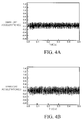
- FIGS. 4A, 4B , 4C, and 4D are graphs obtained by measuring vibratory accelerations of multilayer actuators of Example 1, Example 2, Comparative Example 1, and Comparative Example 2.
- FIGS. 4A, 4B , 4C, and 4D illustrate that Example 1 indicates a vibratory acceleration of about 0.19 G, Example 2 indicates a vibratory acceleration of about 0.27 G, Comparative Example 1 indicates a vibratory acceleration of about 0.10 G, and Comparative Example 2 indicates a vibratory acceleration of about 0.06 G.
- Results of Table 1 and FIGS. 4A, 4B , 4C, and 4D indicate that a driving displacement of a multilayer actuator can be maximized at a constant voltage when disposition and driving as in Example 2 are employed, that is, when electric fields of the same direction are applied to four electroactive layers in a state in which polarization directions of the four electroactive layers are the same.
- results of Table 1 and FIGS. 4A, 4B , 4C, and 4D indicate that a driving displacement of a multilayer actuator can be increased at a constant voltage in a case of disposition and driving as in Example 1, that is, in a case in which electric fields of different directions are applied to four electroactive layers in a state in which displacement directions of the four electroactive layers are the same rather than in a case of disposition and driving as in Example 3, that is, in a case in which electric fields of the same direction are applied to four electroactive layers in a state in which displacement directions of the four electroactive layers are different.
- the results indicate that a driving displacement of a multilayer actuator can be effectively increased when directions of the electroactive layers are the same irrespective of a direction of an electric field applied to each of four electroactive layers.
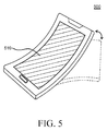
- FIG. 5 is a diagram illustrating a state of a display device 500 to describe variously deformed shapes of the display device 500 according to an embodiment of the present disclosure.
- a description will be given on the assumption that the display device 500 is a smartphone for convenience of description.
- a portion of the display device 500 may be bent upward or downward.
- a multilayer actuator is fixed to a rear surface of a display screen 510, and the multilayer actuator and the whole display device 500 are deformed when the multilayer actuator is driven.
- a portion of the display device 500 may be bent upward or downward.
- the portion of the multilayer actuator is periodically bent upward or downward, the portion of the display device 500 may be bent upward or downward.
- the portion of the multilayer actuator remains bent upward or downward, the portion of the display device 500 may remain bent upward or downward.
- the portion of the display device 500 may be bent upward or downward. That is, when the display device 500 receives a message or a voice call, the portion of the display device 500 may be bent upward or downward as an output in response to the received message or voice call.
- a bent portion, a bending direction, a bending time, a period of change of a bending direction, and the like of the display device 500 may be variously set through the display device 500.
- change of a shape of the display device 500 by the multilayer actuator may be variously set by the user, and is not limited to the above-mentioned example of shape change.
- the multilayer actuator is deformed into different shapes in response to various inputs. Specifically, a bent portion, a bending direction, a bending time, a period of change of a bending direction, and the like may be differently set for each input to the display device 500. Therefore, the display device 500 may be deformed into various shapes by the multilayer actuator, thereby providing the user with various types of outputs.
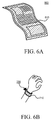
- FIGS. 6A, 6B , and 6C are diagrams illustrating examples in which multilayer actuators according to embodiments of the present disclosure can be advantageously used.
- FIG. 6A is a diagram illustrating an appearance of an electronic newspaper 600 comprising a multilayer actuator according to an embodiment of the present disclosure.
- the electronic newspaper 600 comprises a display panel 610 and the multilayer actuator which is attached to a rear surface of the display panel 610.
- the electronic newspaper 600 comprising the multilayer actuator according to the present embodiment may provide a feeling of actually reading a newspaper by the multilayer actuator.
- the multilayer actuator in a portion receiving the input of the signal may be deformed.
- a portion of the electronic newspaper 600 may be temporarily bent in response to the multilayer actuator being deformed, and thus a feeling of turning a page as a newspaper may be provided.
- a portion of the electronic newspaper 600 is deformed, thereby providing the fact that the article is uploaded.
- the multilayer actuator in a portion comprising the uploaded article is deformed, thereby immediately displaying the fact that the article is uploaded.
- FIG. 6B is a diagram illustrating a watch 700 comprising a multilayer actuator according to an embodiment of the present disclosure.
- the watch 700 comprises a display panel 710 and the multilayer actuator which is attached to a lower portion of the display panel 710.
- the multilayer actuator which is attached to a lower portion of the display panel 710.
- various functions of the watch 700 may be implemented by the multilayer actuator.
- General time information is displayed through the display panel 710 of the watch 700.
- weather, news, and the like may be displayed through the display panel 710 of the watch 700.
- the watch 700 may comprise a simple call function, and determine heart rate of the user wearing the watch 700.
- the multilayer actuator in the watch 700 may be contracted to tell time every hour on the hour or at a designated alarm time. In this way, time information may be provided by pressing a wrist of the user.
- the multilayer actuator in the watch 700 may be contracted when new weather information or a news is displayed, or a protrusion may be formed on a portion of the display panel 710 of the watch 700 when a call is received, thereby providing information. Further, when heart rate of the user measured through a portion of the watch 700 reaches a dangerous level, the multilayer actuator in the watch 700 may be contracted or deformed, thereby a warning alarm to the user.
- FIG. 6C is a diagram illustrating a curtain 800 that comprises a multilayer actuator according to an embodiment of the present disclosure.
- the curtain 800 comprises a display panel 810 and the multilayer actuator which is attached to a lower portion of the display panel 810.
- information about an external environment may be expressed in various manners by the multilayer actuator.
- outside weather may be displayed as a predetermined image through the display panel 810 of the curtain 800, and a specific state of weather may be expressed by changing a shape of the curtain 800.
- a cloud may be displayed through the display panel 810 of the curtain 800, a portion of the curtain 800 may be bent by the multilayer actuator according to a wind direction and a wind speed, and an area of the bent portion may vary.
- a direction in which the curtain 800 may be actually folded or swing according to the wind direction may be expressed as a bending direction of the curtain 800, and the area of the bent portion of the curtain 800 may increase as wind strength increases.
- the curtain 800 may be automatically rolled up or folded in a left or right direction.
- the present disclosure is effective in that a multilayer actuator comprising a plurality of electroactive layers comprising a ferroelectric polymer is allowed to implement a maximum vibratory acceleration at a constant voltage.
- the number of electro-active layers is at least three.
- the present disclosure is effective in that it is possible to provide a clear criterion for a form of arrangement of polarization directions of a plurality of electroactive layers comprised in a multilayer actuator.
- the present disclosure is effective in that it is possible to provide a multilayer actuator having a low driving voltage and suitable for a mobile device.
Landscapes
- Engineering & Computer Science (AREA)
- Theoretical Computer Science (AREA)
- General Engineering & Computer Science (AREA)
- Physics & Mathematics (AREA)
- Computer Hardware Design (AREA)
- Human Computer Interaction (AREA)
- General Physics & Mathematics (AREA)
- Spectroscopy & Molecular Physics (AREA)
- Microelectronics & Electronic Packaging (AREA)
- Devices For Indicating Variable Information By Combining Individual Elements (AREA)
- Electrochromic Elements, Electrophoresis, Or Variable Reflection Or Absorption Elements (AREA)
- Micromachines (AREA)
Abstract
Description
- This application claims the priorities of
Korean Patent Application No. 2014-0195977 filed on December 31, 2014 Korean Patent Application No. 2015-0085104 filed on June 16, 2015 - The present disclosure relates to a multilayer actuator and a display device comprising the same and, more specifically, to a multilayer actuator that can be more greatly displaced at a constant voltage and a display device comprising the same.
- Recently, as users desire to conveniently use various display devices comprising a liquid crystal display (LCD) and an organic light emitting diode (OELD), the use of touch-type display devices, which are touched when receiving inputs, has become common. In this regard, research has been continuously conducted into using an actuator in order to provide direct and various touch feedbacks to users. In addition, research has been conducted into implementing various displacements of a flexible display panel, which has been actively developed, by attaching the actuator to the flexible display panel.
- In general, a conventional display device has employed a vibration motor such as an eccentric rotating mass vibration motor (ERM) or a linear resonance actuator (LRA) as an actuator. The vibration motor is designed to vibrate the whole display device, and thus has a problem that a mass body needs to be increased in size to increase vibration power. In addition, the vibration motor has disadvantages in that frequency modulation for adjusting a level of vibration is difficult, a response speed is significantly low, and the vibration motor is not suitably used for the flexible display device.
- To resolve the above-mentioned issues, a shape memory alloy (SMA) and electro-active ceramics (EAC) have been developed as materials of the actuator. However, the SMA has a low response speed and a short lifespan, and is opaque, and the EAC is fragile. Thus, there has been a difficulty in applying the SMA and the EAC to the display device, in particular, the flexible display device.
- In this regard, an actuator technology using an electro-active polymer (EAP) has been attracting attention of many people. The EAP refers to a polymer that can be deformed by electrical stimulation, and refers to a polymer that can repeatedly expand, contract and bend by electrical stimulation. Research has been conducted such that an actuator comprising the EAP as an electroactive layer is manufactured, and the actuator is attached to the flexible display panel, thereby implementing diverse bending of the display.
- However, bending ability of an actuator comprising only one electroactive layer is restricted due to a thickness thereof, and the actuator has a problem of a high driving voltage. To solve this problem, a multilayer actuator configured by stacking a plurality of unit actuators, each of which comprises one electroactive layer, has been introduced. It has been proved that the multilayer actuator comprising the plurality of electroactive layers can implement a higher driving displacement at the same thickness when compared to the actuator comprising only one electroactive layer.
- In general, an electroactive layer of a unit actuator in a conventional multilayer actuator comprises a dielectric elastomer. The dielectric elastomer does not have polarization in a natural state, and thus former researchers have not considered polarizations of a plurality of electroactive layers. As a result, the former researchers have not considered a form of arrangement of polarization directions of the plurality of electroactive layers.
- However, recently, a ferroelectric polymer, which can ensure a higher driving displacement when compared to the dielectric elastomer, is implemented as an electroactive layer. In essence, the ferroelectric polymer has a natural polarization in a particular direction, and thus there is a need for considering a form of arrangement of polarization directions of a plurality of electroactive layers comprising the ferroelectric polymer in a multilayer actuator. In this regard, there has been introduced scheme of adjusting a direction of an applied electric field for each of the plurality of electroactive layers based on expansion and contraction of the electroactive layers according to the direction of the applied electric field. However, significant effectiveness has not been achieved so far.
- The inventors of the present disclosure has found that, in a multilayer actuator comprising a plurality of electroactive layers comprising a ferroelectric polymer, a driving displacement of the multilayer actuator may be maximized irrespective of a direction of an applied electric field when all of the three or more electroactive layers have the same polarization direction.
- In this regard, an object to be solved by the present disclosure is to provide a multilayer actuator which comprises a plurality of electroactive layers comprising a ferroelectric polymer and has a driving displacement that can be maximized when a constant voltage is applied, and a display device comprising the multilayer actuator.
- Another object to be solved by the present disclosure is to provide a multilayer actuator in which polarization directions of a plurality of electroactive layers are arranged to be optimized in terms of voltage and displacement, and a display device comprising the multilayer actuator.
- Another object to be solved by the present disclosure is to provide a multilayer actuator that can be driven at a low voltage, and a display device comprising the multilayer actuator.
- Technical problems of the present disclosure are not limited to the above-mentioned technical problems, and other technical problems not mentioned herein may be clearly understood by those skilled in the art from description below.
- In order to achieve the above-described object, an aspect of the present disclosure provides a multilayer actuator comprising a plurality of electroactive layers disposed on each other, each comprising a ferroelectric polymer, wherein the polarization directions of all electroactive layers are the same. According to the preferred embodiment of the present invention, the number of electro-active layers is at least three. It has turned out that in an arrangement with three or more electro-active layers, a driving displacement of the multilayer actuator is greatly effected by a form of arrangement of polarization directions of the electro-active layers rather than by the direction of an electric field applied to the electro-active layers.
- According to another feature of the present disclosure, the electroactive layers are made of the same material.
- According to yet another feature of the present disclosure, the electroactive layers may comprise a polyvinylidene fluoride (PVDF)-based polymer.
- According to still another feature of the present disclosure, the electro-active layers have a natural polarization applied by a stretching process or polling process.
- According to still another feature of the present disclosure, the polarization direction of the electroactive layers is perpendicular to the extension direction of the electroactive layers.
- According to still another feature of the present disclosure, the multilayer actuator comprises a plurality of unit actuators disposed on each other, each of these unit actuators comprising one of the electroactive layers, a lower electrode and an upper electrode facing each other with the electro-active layer interposed therebetween. According to another preferred embodiment of the present invention, the number of unit actuators is at least three.
- According to still another feature of the present disclosure, the multilayer actuator is configured to generate an electric field between the lower electrode and the upper electrode of each unit actuator, wherein the direction of the electric field generated in all unit actuators is the same.
- According to still another feature of the present disclosure, the multilayer actuator further comprises a plurality of adhesive layers, with each one adhesive layer disposed between two adjacent unit actuators. According to still another feature of the present disclosure, the adhesive layers comprise a dielectric elastomer and a high-dielectric filler.
- The present invention is further related to a display device, comprising a display panel and a multilayer actuator as described above, which is disposed under a display panel.
- Preferably this display device comprises and upper cover, disposed over the display panel and the multilayer actuator and a lower cover disposed to face the upper cover and disposed below the display panel and the multilayer actuator, wherein the lower cover and the upper cover consist of a material having flexibility.
- According to another preferred embodiment of the present invention, the display panel comprises a flexible substrate.
- The present invention is further related to a method for operating a multilayer actuator as described above, said method comprising the generation of an electric field between the lower electrode and the upper electrode of each unit actuator, wherein the direction of the electric field generated in all unit actuators is the same.
- The above and other aspects, features and other advantages of the present disclosure will be more clearly understood from the following detailed description taken in conjunction with the accompanying drawings, in which:
-
FIG. 1 is a schematic exploded perspective view illustrating a configuration of a display device according to an embodiment of the present disclosure; -
FIG. 2 is a schematic cross-sectional view of a multilayer actuator of the display device according to an embodiment of the present disclosure; -
FIGS. 3A and 3B are diagrams illustrating polarization directions of a first electro-active layer comprising a polyvinylidene fluoride-based polymer; -
FIGS. 4A, 4B ,4C, and 4D are graphs obtained by measuring vibratory accelerations of multilayer actuators of Example 1, Example 2, Comparative Example 1, and Comparative Example 2; -
FIG. 5 is a diagram illustrating a state of the display device to describe variously deformed shapes of the display device according to an embodiment of the present disclosure; and -
FIGS. 6A, 6B , and6C are diagrams illustrating examples in which multilayer actuators according to embodiments of the present disclosure can be advantageously used. - Advantages and features of the present disclosure and methods of accomplishing the same may be understood more readily with reference to the following detailed description of exemplary embodiments and the accompanying drawings. However, the present disclosure will be embodied in many different forms and is not limited to the embodiments set forth herein. Rather, these embodiments make the present disclosure complete, and are provided such that those skilled in the art fully understand the scope of the present disclosure. The present disclosure will be merely defined by the appended claims.
- When an element or layer is described to be "on" another element or layer, the element or layer may be disposed directly on the other element or layer or disposed on the other element or layer with a still another element or layer interposed therebetween.
- Although the terms "first", "second", and the like are used to describe various components, the components are not limited by the terms. The terms are merely used to distinguish one component from another component. Thus, a first component mentioned below may correspond to a second component within the spirit of the present disclosure.
- The same reference numeral refers to the same component throughout the specification.
- A size and a thickness of each configuration illustrated in the drawings are for convenience of description, and the present disclosure is not necessarily limited to the size and thickness of the illustrated configuration.
- Respective features of several embodiments of the present disclosure may be wholly or partially combined or united with each other, and interlocking and driving can be technically configured in various manners. Respective embodiments may be implemented independently of each other or implemented together by being linked to each other.
- Hereinafter, various embodiments of the present disclosure will be described in detail with reference to accompanying drawings.
-
FIG. 1 is a schematic exploded perspective view illustrating a configuration of a display device according to an embodiment of the present disclosure. - Referring to
FIG. 1 , thedisplay device 10 according to the present embodiment comprises anupper cover 100, alower cover 200, aflexible display panel 300, and amultilayer actuator 400. - The
upper cover 100 is disposed over theflexible display panel 300 and themultilayer actuator 400 to cover theflexible display panel 300 and themultilayer actuator 400. Theupper cover 100 protects internal components of thedisplay device 10 from external shock and permeation of water or a foreign material. Theupper cover 100 may be made of a material having a high flexibility, for example, plastic so as to be displaced when themultilayer actuator 400 is displaced by an electric field. - The
lower cover 200 is disposed to face theupper cover 100, and disposed below theflexible display panel 300 and themultilayer actuator 400 to cover theflexible display panel 300 and themultilayer actuator 400. Thelower cover 200 similarly protects internal components of thedisplay device 10 from external shock and permeation of water or a foreign material. Thelower cover 200 may be similarly made of a material having a high flexibility, for example, plastic so as to be displaced when themultilayer actuator 400 is displaced. - The
flexible display panel 300 is disposed between theupper cover 100 and thelower cover 200. Theflexible display panel 300 is a panel having flexibility so as to be bent as paper, and refers to a panel in which a display element for displaying an image is disposed. Theflexible display panel 300 has flexibility, and thus may be displaced together with themultilayer actuator 400 when themultilayer actuator 400 is displaced by an electric field. Theflexible display panel 300 may comprise at least a flexible substrate to ensure flexibility. For example, theflexible display panel 300 may be an organic light-emitting display panel. The organic light-emitting display panel is a display panel in which an organic light-emitting layer emits light when a current is allowed to flow through the organic light-emitting layer. The organic light-emitting display panel emits light having a particular wavelength using the organic light-emitting layer. The organic light-emitting display panel comprises at least a cathode, the organic light-emitting layer, and an anode. - The
multilayer actuator 400 is disposed between theupper cover 100 and thelower cover 200. Themultilayer actuator 400 is disposed below theflexible display panel 300, and is attached to theflexible display panel 300 by an adhesive such as an optical clear adhesive (OCA) or an optical clear resin (OCR). Themultilayer actuator 400 may be displaced in response to expansion or contraction to its electroactive layers. This displacement includes a bending of themultilayer actuator 400. In response to themultilayer actuator 400 being displaced, theupper cover 100, thelower cover 200, and theflexible display panel 300 may be displaced, and thus thewhole display device 10 may be displaced. -
FIG. 2 is a schematic cross-sectional view of the multilayer actuator of the display device according to an embodiment of the present disclosure. - Referring to
FIG. 2 , themultilayer actuator 400 according to the present embodiment comprises afirst unit actuator 410, a firstadhesive layer 420, asecond unit actuator 430, a secondadhesive layer 440, a third unit actuator 450, a third adhesive layer 460, and afourth unit actuator 470. - The
first unit actuator 410 is one unit actuator comprised in themultilayer actuator 400, and configured to be displaced by an electric field. As illustrated inFIG. 2 , thefirst unit actuator 410 comprises a firstlower electrode 412, a first upper electrode 414, and a firstelectroactive layer 416 disposed between the firstlower electrode 412 and the first upper electrode 414. - As shown in
Fig. 2 , thefirst unit actuator 410, thesecond unit actuator 430, the third unit actuator 450 and thefourth unit actuator 470 are disposed on each other in a stacking direction vertical to their extension directions, which correspond to the extension directions of the respective electro-active layers 416,436,456,476 comprised within the unit actuators 410,430,450,470. - The first
lower electrode 412 and the first upper electrode 414 perform a function of forming an electric field in the firstelectroactive layer 416 by receiving a voltage applied from outside. There should be a potential difference between the firstlower electrode 412 and the first upper electrode 414 to form the electric field in the firstelectroactive layer 416. Therefore, voltages having different levels are applied to the firstlower electrode 412 and the first upper electrode 414. For example, while a positive voltage is applied to the firstlower electrode 412, a ground voltage may be applied to the first upper electrode 414. Alternatively, while a negative voltage is applied to the firstlower electrode 412, a ground voltage may be applied to the first upper electrode 414. - The electric field may be formed in the first
electroactive layer 416 in a different direction according to a level of a voltage applied to each of the firstlower electrode 412 and the first upper electrode 414. For example, when a voltage applied to the firstlower electrode 412 is lower than a voltage applied to the first upper electrode 414, an electric field may be formed upward in the firstelectroactive layer 416. On the other hand, when a voltage applied to the first upper electrode 414 is higher than a voltage applied to the firstlower electrode 412, an electric field may be formed downward in the firstelectroactive layer 416. - An alternating current (AC) voltage or a direct current (DC) voltage may be applied to the first
lower electrode 412 and the first upper electrode 414. When the AC voltage is applied to the firstlower electrode 412 and the first upper electrode 414, thefirst unit actuator 410 may be periodically displaced. When the DC voltage is applied to the firstlower electrode 412 and the first upper electrode 414, thefirst unit actuator 410 may be maintained in a bent state. - The first
lower electrode 412 and the first upper electrode 414 may be made of a conductive material. For example, the firstlower electrode 412 and the first upper electrode 414 may be made of a metal material such as gold (Au), copper (Cu), titanium (Ti), chrome (Cr), molybdenum (Mo), aluminum (Al), an Al-Cu alloy, or a conductive polymer such as PEDOT[Poly(3,4-EthyleneDiOxyThiophene)]:PSS [Poly(4-StyreneSulfonic acid)], polypyrrole, polyaniline. However, the present disclosure is not limited thereto. The firstlower electrode 412 and the first upper electrode 414 may be made of the same material or different materials. - As thicknesses of electrodes disposed on a lower surface and an upper surface of an electroactive layer increase, the number of electroactive layers comprised in a multilayer actuator having a constant thickness decreases. considering that a driving displacement of the multilayer actuator increases as the number of electroactive layers increases, it is preferable that the thicknesses of the electrodes disposed on the lower surface and the upper surface of the electroactive layer are as thin as possible in order to dispose as many electroactive layers as possible in the multilayer actuator having the constant thickness. For example, it is preferable that thickness of the first
lower electrode 412 and the first upper electrode 414 disposed on a lower surface and an upper surface of the firstelectroactive layer 416 is in a range of 50 nm to 100 nm. - When the same voltage is applied to the first
lower electrode 412 and the first upper electrode 414, strength of an electric field formed in the firstelectroactive layer 416 increases as sheet resistances of the firstlower electrode 412 and the first upper electrode 414 decrease. Therefore, it is preferable that the firstlower electrode 412 and the first upper electrode 414 have as low sheet resistance as possible, for example, a sheet resistance of 200 Ω/sq or less. - The first
lower electrode 412 and the first upper electrode 414 may be disposed on both surfaces of the firstelectroactive layer 416 using various processes. For example, the firstlower electrode 412 and the first upper electrode 414 may be disposed on both surfaces of the firstelectroactive layer 416 using a process such as sputtering, printing, and slit coating. In particular, when the firstlower electrode 412 and the first upper electrode 414 are made of the same material, the firstlower electrode 412 and the first upper electrode 414 may be simultaneously disposed in the same process. - The first
electroactive layer 416 may be disposed between the firstlower electrode 412 and the first upper electrode 414 and displaced by an electric field formed by the firstlower electrode 412 and the first upper electrode 414. - The first
electroactive layer 416 comprises a ferroelectric polymer which has a polarization in a natural state. For example, the firstelectroactive layer 416 comprises a polyvinylidene fluoride (PVDF)-based polymer such as a PVDF homopolymer or a PVDF copolymer. A displacement of the firstelectroactive layer 416 may be induced by applying an electric field to the firstelectroactive layer 416 which has a polarization in a particular direction, for example, upward or downward. The terms "upward" and "downward" refer to directions perpendicular to the extension direction of the respective electro-active layer, i.e. a direction parallel to the stacking direction of the electro-active layers disposed on each other. - A polarization direction of the first
electroactive layer 416 may be determined according to an arrangement of atoms comprised in the firstelectroactive layer 416. InFIGS. 3A and 3B , the polarization direction of the firstelectroactive layer 416 will be covered on the assumption that the firstelectroactive layer 416 comprises the polyvinylidene fluoride-based polymer. -
FIGS. 3A and 3B are diagrams illustrating polarization directions of the first electroactive layer comprising the polyvinylidene fluoride-based polymer. - Referring to
FIG. 3A , it can be understood that the polarization direction of the firstelectroactive layer 416 corresponds to an upward direction since fluorine (F) atoms comprising a lot of electrons are disposed in a lower part and hydrogen (H) atoms comprising few electrons are disposed in an upper part in the firstelectroactive layer 416. In the polyvinylidene fluoride-based polymer, the polarization direction may be defined as a direction from the F atoms to the H atoms. - Referring to
FIG. 3B , it can be understood that the polarization direction of the firstelectroactive layer 416 corresponds to a downward direction since F atoms comprising a lot of electrons are disposed in an upper part and H atoms comprising few electrons are disposed in a lower part in the firstelectroactive layer 416. - The first
electroactive layer 416 may be manufactured using co-extrusion process rather than a solution casting process. When an electroactive layer is manufactured using a dielectric elastomer such as polydimethyl siloxane (PDMS), the solution casting process is generally used to apply a solution to a substrate and dry the solution. This is because the dielectric elastomer may ensure a permittivity of a certain level using a simple solution casting process. However, the ferroelectric polymer such as the polyvinylidene fluoride-based polymer may not ensure a high permittivity using the solution casting process, and thus ensures a high permittivity using co-extrusion process and furthermore using a stretching process or a polling process. - In this regard, the first
electroactive layer 416 may be a film subjected to the stretching process or the polling process. The stretching process refers to a process of pulling and orienting a polymer chain in a heated state, and the polling process refers to a process of arranging atoms having particular charges in one direction by applying a high DC voltage to a polymer. When the stretching process or the polling process is applied to the firstelectroactive layer 416, the firstelectroactive layer 416 may function as an electroactive layer by ensuring a high permittivity. For example, PVDF corresponding to the PVDF homopolymer may function as an electroactive layer by being stretched and polled, and P(VDF-TrFE)(Poly(VinyliDene Fluoride)-trifluoroethylene corresponding to the PVDF copolymer may function as an electroactive layer by being polled. - When the first
electroactive layer 416 is manufactured using co-extrusion process and furthermore using the stretching process or the polling process, configuring thefirst unit actuator 410 as the firstlower electrode 412, the first upper electrode 414, and the firstelectroactive layer 416 as illustrated inFIG. 2 may be advantageous in terms of a driving displacement when compared to configuring thefirst unit actuator 410 merely as one electrode and a first electroactive layer. As a distance between two electrodes decreases, strength of an electric field generated by the same driving voltage increases. While only the firstelectroactive layer 416 is present between two electrodes, that is, the firstlower electrode 412 and the first upper electrode 414 in the former case, an adhesive layer that bonds two unit actuators together is further present in addition to the first electroactive layer between the two electrodes in the latter case. Thus, the distance between the two electrodes is shorter in the former case than in the latter case. - A thickness of the first
electroactive layer 416 may be freely selected by those skilled in the art based on power consumption and a driving voltage necessary to operate as thefirst unit actuator 410 and whether a normal operation as thefirst unit actuator 410 can be performed. The thickness of the firstelectroactive layer 416 may be preferably 50 µm to 400 µm. The thickness of the firstelectroactive layer 416 may be more preferably 100 µm to 300 µm. Here, when the thickness of the firstelectroactive layer 416 is less than 50 µm, a sufficient voltage necessary for a normal operation of thefirst unit actuator 410 may not be applied. Therefore, thefirst unit actuator 410 may not normally operate. In addition, when the thickness of the firstelectroactive layer 416 is greater than 400 µm, a high driving voltage is required to generate Maxwell stress necessary for the normal operation of thefirst unit actuator 410, and thus power consumption may excessively increase. - The first
adhesive layer 420 is disposed between thefirst unit actuator 410 and thesecond unit actuator 430 to perform a function of bonding thefirst unit actuator 410 and thesecond unit actuator 430 together. An OCA or an OCR may be used as the firstadhesive layer 420. A high dielectric adhesive layer obtained by adding a high dielectric filler to a dielectric elastomer may be preferably used. Here, the dielectric elastomer may correspond to at least one material selected from the group consisting of an acrylic-based polymer, a urethane-based polymer, and a silicone-based polymer, and preferably correspond to polydimethyl siloxane (PDMS). The high dielectric filler may correspond to at least one material selected from the group consisting of piezoelectric ceramics, carbon nanoparticles, metal nanoparticles, and a conductive polymer, and preferably correspond to piezoelectric ceramics such as barium titanate (BaTiO3). - The high dielectric adhesive layer has a high permittivity, and thus may perform a function as another electroactive layer in addition to a function as an adhesive layer. Specifically, the high dielectric adhesive layer may perform a function as another electroactive layer that is deformed by an electric field applied by adjacent electrodes, that is, the first
lower electrode 412 of thefirst unit actuator 410 and a second upper electrode 434 of thesecond unit actuator 430 in addition to a function as an adhesive layer that bonds thefirst unit actuator 410 and thesecond unit actuator 430 together. Therefore, when the high dielectric adhesive layer obtained by adding the high dielectric filler to the dielectric elastomer is employed as the firstadhesive layer 420, a driving displacement of themultilayer actuator 400 in the same electric field may be enhanced, and a total permittivity of themultilayer actuator 400 may increase. - Each of the
second unit actuator 430, the third unit actuator 450, and thefourth unit actuator 470 is one unit actuator comprised in themultilayer actuator 400, and configured to be displaced by an electric field. - As illustrated in
FIG. 2 , thesecond unit actuator 430 comprises a secondlower electrode 432, the second upper electrode 434, and a secondelectroactive layer 436, the third unit actuator 450 comprises a third lower electrode 453, a third upper electrode 454, and a third electroactive layer 456, and thefourth unit actuator 470 comprises a fourthlower electrode 472, a fourth upper electrode 474, and a fourthelectroactive layer 476. - Here, each of the second
electroactive layer 436, the third electroactive layer 456, and the fourthelectroactive layer 476 comprises a ferroelectric polymer which has polarization in a natural state, and configured to be displaced by an electric field. Further, all of the firstelectroactive layer 416, the secondelectroactive layer 436, the third electroactive layer 456, and the fourthelectroactive layer 476 have the same polarization direction. For example, as illustrated inFIG. 2 , all polarization directions of the firstelectroactive layer 416, the secondelectroactive layer 436, the third electroactive layer 456, and the fourthelectroactive layer 476 correspond to the upward direction. - When a multilayer actuator comprises only two electroactive layers, a driving displacement of the multilayer actuator is greatly affected by a direction of an electric field applied to each of the plurality of electroactive layers rather than a form of arrangement of polarization directions of the plurality of electroactive layers. However, when a multilayer actuator comprises three or more electroactive layers, a driving displacement of the multilayer actuator is greatly affected by a form of arrangement of polarization directions of the electroactive layers rather than an electric field applied to the electroactive layers.
- In this regard, in the
multilayer actuator 400 according to the present embodiment, a driving displacement of themultilayer actuator 400 is maximized by setting all the polarization directions of the firstelectroactive layer 416, the secondelectroactive layer 436, the third electroactive layer 456, and the fourthelectroactive layer 476 to the same direction. When themultilayer actuator 400 comprises three or moreelectroactive layers electroactive layers electroactive layers active layers - Even when the polarization directions of all
electroactive layers multilayer actuator 400 is partially affected by the direction of the electric field. Specifically, even when the polarization directions of all of theelectroactive layers electroactive layers electroactive layers FIGS. 4A, 4B ,4C, and 4D . - The first
electroactive layer 416, the secondelectroactive layer 436, the third electroactive layer 456, and the fourthelectroactive layer 476 may be made of the same material, for example, the polyvinylidene fluoride-based polymer. When the firstelectroactive layer 416, the secondelectroactive layer 436, the third electroactive layer 456, and the fourthelectroactive layer 476 are made of the same material, co-extrusion process, the stretching process, and the polling process may be performed at one time, and thus it is possible to attempt simplification of a manufacturing process of themultilayer actuator 400. In addition, the firstelectroactive layer 416, the secondelectroactive layer 436, the third electroactive layer 456, and the fourthelectroactive layer 476 similarly behave at a constant voltage, and thus it has an advantage in predicting a driving displacement of themultilayer actuator 400. - The above description related to the first
electroactive layer 416 may be adopted without change for thicknesses, formation methods, and the like of the secondelectroactive layer 436, the third electroactive layer 456, and the fourthelectroactive layer 476, and thus repeated description will be omitted. In addition, the secondlower electrode 432, the thirdlower electrode 452, and the fourthlower electrode 472 may be configured to be substantially the same as the firstlower electrode 412. Further, the second upper electrode 434, the third upper electrode 454, and the fourth upper electrode 474 may be configured to be substantially the same as the first upper electrode 414. Thus, repeated description will be omitted. - The second
adhesive layer 440 is disposed between thesecond unit actuator 430 and the third unit actuator 450, and the third adhesive layer 460 is disposed between the third unit actuator 450 and thefourth unit actuator 470. The secondadhesive layer 440 and the third adhesive layer 460 may be configured to be substantially the same as the firstadhesive layer 420, and thus repeated description will be omitted. - For convenience of description, the
multilayer actuator 400 ofFIG. 2 is described to comprise the fourunit actuators adhesive layers unit actuators adjacent unit actuators und 470. A radius curvature and a vibratory acceleration of a multilayer actuator comprising four electroactive layers disposed in the same polarization direction as illustrated inFIG. 2 were measured by varying directions of electric fields applied to the four electroactive layers in a state in which the multilayer actuator is attached to a flexible display panel in order to examine an effect of the present disclosure. Furthermore, a radius curvature and a vibratory acceleration of a multilayer actuator comprising four electroactive layers disposed in different polarization directions were measured by varying directions of electric fields applied to the four electroactive layers in a state in which the multilayer actuator is attached to a flexible display panel. - In Example 1, an experiment was conducted such that a multilayer actuator in which all polarization directions of four electroactive layers are disposed upward is attached to a flexible display panel, downward electric fields are applied to a first electroactive layer and a third electroactive layer, and upward electric fields are applied to a second electroactive layer and a fourth electroactive layer. To this end, positive voltages were applied to a first upper electrode, a second lower electrode, a third upper electrode, and a fourth lower electrode, and negative voltages were applied to a first lower electrode, a second upper electrode, a third lower electrode, and a fourth upper electrode.
- In Example 2, an experiment was conducted such that downward electric fields are applied to all a first electroactive layer, a second electroactive layer, a third electroactive layer, and a fourth electroactive layer in a state in which a multilayer actuator in which all polarization directions of the four electroactive layers are arranged upward is attached to a flexible display panel. To this end, positive voltages were applied to a first upper electrode, a second upper electrode, a third upper electrode, and a fourth upper electrode, and negative voltages were applied to a first lower electrode, a second lower electrode, a third lower electrode, and a fourth lower electrode.
- In Comparative Example 1, a multilayer actuator, in which polarization directions of four electroactive layers are arranged such that different polarization directions are alternately arranged, was prepared. Specifically, in the prepared multilayer actuator, polarization directions of a first electroactive layer and a third electroactive layer were arranged upward, and polarization directions of a second electroactive layer and a fourth electroactive layer were arranged downward. Then, an experiment was conducted such that downward electric fields are applied to the first electroactive layer and the third electroactive layer and upward electric fields are applied to the second electroactive layer and the fourth electroactive layer in a state in which the multilayer actuator is attached to a flexible display panel.
- In Comparative Example 2, an experiment was conducted such that downward electric fields are applied to all of a first electroactive layer, a second electroactive layer, a third electroactive layer, and a fourth electroactive layer in a station in which the multilayer actuator as in Comparative Example 1 is attached to a flexible display panel.
- In Example 1, Example 2, Comparative Example 1, and Comparative Example 2, the same condition was applied except for polarization directions of four electroactive layer and directions of electric fields applied to the four electroactive layer. Specifically, in each of Example 1, Example 2, Comparative Example 1, and Comparative Example 2, a PVDF homopolymer was subject to a stretching process and a polling process, and then the PVDF homopolymer was laminated to prepare four electroactive layers, and metal electrodes were deposited on both surfaces of each of the electroactive layers, thereby manufacturing four unit actuators. Polarization directions of the four electroactive layers were measured using polarization direction measuring equipment (APC International, Ltd., 90-2030), a maximum radius curvature and a minimum radius curvature were measured under a condition of 4.2 kVpp, and a vibratory acceleration was measured under a condition of 100 kHz and 1.4 kVpp.
- Table 1 below lists a maximum radius curvature, a minimum radius curvature, and a radius curvature change value of each of Example 1, Example 2, Comparative Example 1, and Comparative Example 2.
[Table 1] Minimum radius curvature(mm) Maximum radius curvature(mm) Radius curvature change value Example 1 938 1682 744 Example 2 741 1755 1014 Comparative Example 1 983 1563 580 Comparative Example 2 1303 1617 314 -
FIGS. 4A, 4B ,4C, and 4D are graphs obtained by measuring vibratory accelerations of multilayer actuators of Example 1, Example 2, Comparative Example 1, and Comparative Example 2. -
FIGS. 4A, 4B ,4C, and 4D illustrate that Example 1 indicates a vibratory acceleration of about 0.19 G, Example 2 indicates a vibratory acceleration of about 0.27 G, Comparative Example 1 indicates a vibratory acceleration of about 0.10 G, and Comparative Example 2 indicates a vibratory acceleration of about 0.06 G. - Results of Table 1 and
FIGS. 4A, 4B ,4C, and 4D indicate that a driving displacement of a multilayer actuator can be maximized at a constant voltage when disposition and driving as in Example 2 are employed, that is, when electric fields of the same direction are applied to four electroactive layers in a state in which polarization directions of the four electroactive layers are the same. - In addition, results of Table 1 and
FIGS. 4A, 4B ,4C, and 4D indicate that a driving displacement of a multilayer actuator can be increased at a constant voltage in a case of disposition and driving as in Example 1, that is, in a case in which electric fields of different directions are applied to four electroactive layers in a state in which displacement directions of the four electroactive layers are the same rather than in a case of disposition and driving as in Example 3, that is, in a case in which electric fields of the same direction are applied to four electroactive layers in a state in which displacement directions of the four electroactive layers are different. The results indicate that a driving displacement of a multilayer actuator can be effectively increased when directions of the electroactive layers are the same irrespective of a direction of an electric field applied to each of four electroactive layers. -
FIG. 5 is a diagram illustrating a state of adisplay device 500 to describe variously deformed shapes of thedisplay device 500 according to an embodiment of the present disclosure. InFIG. 5 , a description will be given on the assumption that thedisplay device 500 is a smartphone for convenience of description. - Referring to
FIG. 5 , a portion of thedisplay device 500 may be bent upward or downward. Specifically, a multilayer actuator is fixed to a rear surface of adisplay screen 510, and the multilayer actuator and thewhole display device 500 are deformed when the multilayer actuator is driven. In other words, when a portion of the multilayer actuator is bent upward or downward, a portion of thedisplay device 500 may be bent upward or downward. Here, when the portion of the multilayer actuator is periodically bent upward or downward, the portion of thedisplay device 500 may be bent upward or downward. In addition, when the portion of the multilayer actuator remains bent upward or downward, the portion of thedisplay device 500 may remain bent upward or downward. - For example, as an output in response to a touch input to the
display device 500 by a user, the portion of thedisplay device 500 may be bent upward or downward. That is, when thedisplay device 500 receives a message or a voice call, the portion of thedisplay device 500 may be bent upward or downward as an output in response to the received message or voice call. - A bent portion, a bending direction, a bending time, a period of change of a bending direction, and the like of the
display device 500 may be variously set through thedisplay device 500. In other words, change of a shape of thedisplay device 500 by the multilayer actuator may be variously set by the user, and is not limited to the above-mentioned example of shape change. - In the
display device 500 comprising the multilayer actuator according to the present embodiment, the multilayer actuator is deformed into different shapes in response to various inputs. Specifically, a bent portion, a bending direction, a bending time, a period of change of a bending direction, and the like may be differently set for each input to thedisplay device 500. Therefore, thedisplay device 500 may be deformed into various shapes by the multilayer actuator, thereby providing the user with various types of outputs. -
FIGS. 6A, 6B , and6C are diagrams illustrating examples in which multilayer actuators according to embodiments of the present disclosure can be advantageously used. -
FIG. 6A is a diagram illustrating an appearance of anelectronic newspaper 600 comprising a multilayer actuator according to an embodiment of the present disclosure. Referring toFIG. 6A , theelectronic newspaper 600 comprises adisplay panel 610 and the multilayer actuator which is attached to a rear surface of thedisplay panel 610. - The
electronic newspaper 600 comprising the multilayer actuator according to the present embodiment may provide a feeling of actually reading a newspaper by the multilayer actuator. When a signal for turning a page is input through thedisplay panel 610 of theelectronic newspaper 600, the multilayer actuator in a portion receiving the input of the signal may be deformed. In this way, a portion of theelectronic newspaper 600 may be temporarily bent in response to the multilayer actuator being deformed, and thus a feeling of turning a page as a newspaper may be provided. - In addition, when a new article is uploaded and displayed on the
electronic newspaper 600 that comprises the multilayer actuator according to the present embodiment, a portion of theelectronic newspaper 600 is deformed, thereby providing the fact that the article is uploaded. For example, when an article having a new headline is uploaded, the multilayer actuator in a portion comprising the uploaded article is deformed, thereby immediately displaying the fact that the article is uploaded. -
FIG. 6B is a diagram illustrating awatch 700 comprising a multilayer actuator according to an embodiment of the present disclosure. Referring toFIG. 6B , thewatch 700 comprises adisplay panel 710 and the multilayer actuator which is attached to a lower portion of thedisplay panel 710. Here, a description will be given on the assumption that thewatch 700 is a smart watch for convenience of description. - In the
watch 700 comprising the multilayer actuator according to the present embodiment, various functions of thewatch 700 may be implemented by the multilayer actuator. General time information is displayed through thedisplay panel 710 of thewatch 700. In addition, weather, news, and the like may be displayed through thedisplay panel 710 of thewatch 700. Further, thewatch 700 may comprise a simple call function, and determine heart rate of the user wearing thewatch 700. Here, the multilayer actuator in thewatch 700 may be contracted to tell time every hour on the hour or at a designated alarm time. In this way, time information may be provided by pressing a wrist of the user. In addition, the multilayer actuator in thewatch 700 may be contracted when new weather information or a news is displayed, or a protrusion may be formed on a portion of thedisplay panel 710 of thewatch 700 when a call is received, thereby providing information. Further, when heart rate of the user measured through a portion of thewatch 700 reaches a dangerous level, the multilayer actuator in thewatch 700 may be contracted or deformed, thereby a warning alarm to the user. -
FIG. 6C is a diagram illustrating acurtain 800 that comprises a multilayer actuator according to an embodiment of the present disclosure. Referring toFIG. 6C , thecurtain 800 comprises adisplay panel 810 and the multilayer actuator which is attached to a lower portion of thedisplay panel 810. - In the
curtain 800 comprising the multilayer actuator according to present embodiment, information about an external environment may be expressed in various manners by the multilayer actuator. Specifically, outside weather may be displayed as a predetermined image through thedisplay panel 810 of thecurtain 800, and a specific state of weather may be expressed by changing a shape of thecurtain 800. For example, when a wind blows in a cloudy weather, a cloud may be displayed through thedisplay panel 810 of thecurtain 800, a portion of thecurtain 800 may be bent by the multilayer actuator according to a wind direction and a wind speed, and an area of the bent portion may vary. In other words, a direction in which thecurtain 800 may be actually folded or swing according to the wind direction may be expressed as a bending direction of thecurtain 800, and the area of the bent portion of thecurtain 800 may increase as wind strength increases. In addition, when intensity of light entering through a window becomes less than or equal to a certain level, thecurtain 800 may be automatically rolled up or folded in a left or right direction. - The present disclosure is effective in that a multilayer actuator comprising a plurality of electroactive layers comprising a ferroelectric polymer is allowed to implement a maximum vibratory acceleration at a constant voltage. According to a preferred embodiment, the number of electro-active layers is at least three.
- The present disclosure is effective in that it is possible to provide a clear criterion for a form of arrangement of polarization directions of a plurality of electroactive layers comprised in a multilayer actuator.
- The present disclosure is effective in that it is possible to provide a multilayer actuator having a low driving voltage and suitable for a mobile device.
- Effects that may be obtained from the present disclosure are not limited to the above-mentioned effects, and other effects not mentioned herein may be clearly understood by those skilled in the art from the above description.
- Embodiments of the present disclosure have been described in more detail with reference to the accompanying drawings. However, the present disclosure is not restricted to the embodiments, and may be variously changed and implemented within the scope of the technical spirit of the present disclosure. Thus, the embodiments are disclosed to describe the technical spirit of the present disclosure rather than to restrict the technical spirit. The scope of the technical spirit of the present disclosure is not restricted by the embodiments. Therefore, the above-described embodiments should be understood illustratively rather than restrictively in all aspects. The scope of the present disclosure should be interpreted by claims below, and all technical spirits within an equivalent range thereof should be construed as being comprised in the scope of the present disclosure.
Claims (15)
- Multilayer actuator (400), comprising a plurality of electroactive layers (416, 436, 456, 476) disposed on each other, each comprising a ferroelectric polymer (416, 436, 456, 476), wherein the polarization directions of all electroactive layers (416, 436, 456, 476) are the same.
- Multilayer actuator (400) according to claim 1, wherein the number of electroactive layers (416, 436, 456, 476) is at least three.
- Multilayer actuator (400) according to claim 1 or 2, wherein the electroactive layers (416, 436, 456, 476) are made of the same material.
- Multilayer actuator (400) according to one of the preceding claims, wherein the electroactive layers (416, 436, 456, 476) comprise a polyvinyldene fluoride (PVDF)-based polymer.
- Multilayer actuator (400) according to one of the preceding claims, wherein the electroactive layers (416, 436, 456, 476) have a natural polarization applied by a stretching process or polling process.
- Multilayer actuator (400) according to one of the preceding claims, wherein the polarization direction of the electroactive layers (416, 436, 456, 476) is perpendicular to the extension direction of the electroactive layers (416,436, 456,476).
- Multilayer actuator (400) according to one of the preceding claims, comprising a plurality of unit actuators (410, 430, 450, 470) disposed on each other, each of these unit actuators (410, 430, 450, 470) comprising one of the electroactive layers (416, 436, 456, 476), a lower electrode (412, 432, 452, 472) and an upper electrode (414, 434, 454, 474) facing each other with the electroactive layer interposed therebetween.
- Multilayer actuator (400) according to claim 7, wherein the number of unit actuators (410, 430, 450, 470) is at least three.
- Multilayer actuator (400) according to claim 7 or 8, which is configured to generate an electric field between the lower electrode (412, 432, 452, 472) and the upper electrode (414, 434, 454, 474) of each unit actuator (410, 430, 450, 470), wherein the direction of the electric field generated in all unit actuators (410, 430, 450, 470) is the same.
- Multilayer actuator (400) according to one of claims 7 to 9, comprising a plurality of adhesive layers (420, 440, 460), with each one adhesive layer (420, 440, 460), disposed between two adjacent unit actuators (410, 430, 450, 470).
- Multilayer actuator (400) according to claim 10, wherein the adhesive layers (420, 440, 460) comprise a dielectric elastomer and a high-dielectric filler.
- Display device (10), comprising a display panel (300) and a multilayer actuator (400) according to one of the preceding claims, which is disposed under the display panel (300).
- Display device (10) according to claim 1, comprising an upper cover (100) disposed over the display panel (300) and the multilayer actuator (400) and a lower cover (200) disposed to face the upper cover (100) and disposed below the display panel (300) and the multilayer actuator (400), wherein the lower cover (200) and the upper cover (100) consist of a material having flexibility.
- Display device (10) according to claim 12 or 13, wherein the display panel (300) comprises a flexible substrate.
- Method for operating a multilayer actuator (400) according to one of claims 1 to 11, comprising the generation of an electric field between the lower electrode (412, 432, 452, 472) and upper electrode (414, 434, 454, 474) of each unit actuator (410, 430, 450, 470), wherein the direction of the electric field generated in all unit actuators (410, 430, 450, 470) is the same.
Applications Claiming Priority (2)
| Application Number | Priority Date | Filing Date | Title |
|---|---|---|---|
| KR20140195977 | 2014-12-31 | ||
| KR1020150085104A KR102381743B1 (en) | 2014-12-31 | 2015-06-16 | Multilayer actuator and display device comprising the same |
Publications (2)
| Publication Number | Publication Date |
|---|---|
| EP3041059A1 true EP3041059A1 (en) | 2016-07-06 |
| EP3041059B1 EP3041059B1 (en) | 2019-09-11 |
Family
ID=54783430
Family Applications (1)
| Application Number | Title | Priority Date | Filing Date |
|---|---|---|---|
| EP15197808.7A Not-in-force EP3041059B1 (en) | 2014-12-31 | 2015-12-03 | Multilayer actuator and display device comprising the same |
Country Status (4)
| Country | Link |
|---|---|
| US (1) | US9748469B2 (en) |
| EP (1) | EP3041059B1 (en) |
| JP (1) | JP6231542B2 (en) |
| CN (1) | CN105810814B (en) |
Cited By (1)
| Publication number | Priority date | Publication date | Assignee | Title |
|---|---|---|---|---|
| EP4276575A4 (en) * | 2021-03-05 | 2024-11-13 | Samsung Electronics Co., Ltd. | DISPLAY STRUCTURE COMPRISING A DIELECTRIC LAYER AND ELECTRONIC DEVICE COMPRISING SAME |
Families Citing this family (14)
| Publication number | Priority date | Publication date | Assignee | Title |
|---|---|---|---|---|
| CN105138076B (en) * | 2015-08-03 | 2020-01-31 | 联想(北京)有限公司 | Control method of electronic devices and electronic device |
| KR20170073149A (en) * | 2015-12-18 | 2017-06-28 | 삼성전자주식회사 | Performing task and electronic device supporting the same |
| KR102483412B1 (en) * | 2015-12-31 | 2022-12-29 | 엘지디스플레이 주식회사 | Touch sensitive device and display device comprising the same |
| EP3463091B1 (en) * | 2016-08-25 | 2019-10-09 | Koninklijke Philips N.V. | Variable focus x-ray anti scatter device |
| US10396272B2 (en) * | 2017-05-04 | 2019-08-27 | International Business Machines Corporation | Display distortion for alignment with a user gaze direction |
| US10901510B2 (en) * | 2018-10-09 | 2021-01-26 | Microsoft Technology Licensing, Llc | Haptic feedback system having two independent actuators |
| US11632063B1 (en) * | 2019-08-27 | 2023-04-18 | Meta Platforms Technologies, Llc | Structured actuators |
| WO2021070809A1 (en) * | 2019-10-08 | 2021-04-15 | ソニー株式会社 | Actuator, method of manufacturing same, driving device, and electronic equipment |
| CN111152210B (en) * | 2020-01-17 | 2021-05-07 | 浙江大学 | A Flexible Electrohydrodynamic Actuator |
| CN115244720A (en) * | 2020-03-19 | 2022-10-25 | 富士胶片株式会社 | Laminated piezoelectric element and electroacoustic transducer |
| DE102020112725A1 (en) | 2020-05-11 | 2021-11-11 | Technische Universität Dresden | FLEXIBLE DISPLAY DEVICE, METHOD FOR STABILIZING AT LEAST ONE GEOMETRIC CONFIGURATION OF A FLEXIBLE DISPLAY DEVICE, ROLLABLE PROJECTION SCREEN, AND METHOD FOR STABILIZING A ROLLED CONFIGURATION OF A ROLLED PROJECTION WALL |
| US12047721B2 (en) * | 2020-08-31 | 2024-07-23 | Lg Display Co., Ltd. | Vibration apparatus and apparatus including the same |
| KR102787617B1 (en) * | 2020-10-21 | 2025-03-26 | 엘지디스플레이 주식회사 | Vibration apparatus and apparatus comprising the same |
| KR20230094707A (en) * | 2021-12-21 | 2023-06-28 | 엘지디스플레이 주식회사 | Apparatus |
Citations (3)
| Publication number | Priority date | Publication date | Assignee | Title |
|---|---|---|---|---|
| DE2742977A1 (en) * | 1976-09-24 | 1978-03-30 | Pennwalt Corp | METHOD FOR POLARIZING A MULTI-LAYER STACK OF INDIVIDUAL PIEZOELECTRIC-FORMING RESIN MEMBRANES OR - FILMS |
| US5700359A (en) * | 1995-02-17 | 1997-12-23 | Institut Franco Allemand De Recherches De Saint-Louis | Method of polarizing at least one large area sheet of ferroelectric material |
| US5703425A (en) * | 1993-01-29 | 1997-12-30 | Thomson-Csf | Process for manufacturing a piezoelectric component |
Family Cites Families (49)
| Publication number | Priority date | Publication date | Assignee | Title |
|---|---|---|---|---|
| US4245172A (en) * | 1976-11-02 | 1981-01-13 | The United States Of America As Represented By The Secretary Of The Navy | Transducer for generation and detection of shear waves |
| US4330730A (en) * | 1980-03-27 | 1982-05-18 | Eastman Kodak Company | Wound piezoelectric polymer flexure devices |
| JPS5931078A (en) * | 1982-08-13 | 1984-02-18 | Omron Tateisi Electronics Co | Piezoelectric bimorph |
| JPS59211291A (en) * | 1983-05-17 | 1984-11-30 | Kureha Chem Ind Co Ltd | Electrical-mechanical converter |
| JPS59222977A (en) * | 1983-06-01 | 1984-12-14 | Nippon Soken Inc | Piezoelectric body actuator |
| US4833659A (en) * | 1984-12-27 | 1989-05-23 | Westinghouse Electric Corp. | Sonar apparatus |
| US4868447A (en) * | 1987-09-11 | 1989-09-19 | Cornell Research Foundation, Inc. | Piezoelectric polymer laminates for torsional and bending modal control |
| JPH02197183A (en) * | 1988-03-29 | 1990-08-03 | Pennwalt Corp | Laminated piezoelectric structure and its forming method |
| US5166573A (en) * | 1989-09-26 | 1992-11-24 | Atochem North America, Inc. | Ultrasonic contact transducer and array |
| EP0441438B1 (en) * | 1990-02-07 | 1995-06-28 | Koninklijke Philips Electronics N.V. | Method of producing a multilayer piezoelectric element as well as multilayer piezoelectric element |
| US5285551A (en) * | 1992-02-06 | 1994-02-15 | Prince Corporation | Assist strap |
| FR2691596B1 (en) * | 1992-05-22 | 1995-04-28 | Thomson Csf | Acoustic underwater antenna with area sensor. |
| US5367500A (en) * | 1992-09-30 | 1994-11-22 | The United States Of America As Represented By The Secretary Of The Navy | Transducer structure |
| US5835453A (en) * | 1993-07-20 | 1998-11-10 | The United States Of America As Represented By The Secretary Of The Navy | Electrostrictive acoustic projector and polymers used therein |
| US5608692A (en) * | 1994-02-08 | 1997-03-04 | The Whitaker Corporation | Multi-layer polymer electroacoustic transducer assembly |
| US5559387A (en) * | 1994-05-13 | 1996-09-24 | Beurrier; Henry R. | Piezoelectric actuators |
| US5440194A (en) * | 1994-05-13 | 1995-08-08 | Beurrier; Henry R. | Piezoelectric actuators |
| US6812624B1 (en) * | 1999-07-20 | 2004-11-02 | Sri International | Electroactive polymers |
| JP2002513514A (en) * | 1997-11-18 | 2002-05-08 | ザ ペンステート リサーチファウンデーション | Ferroelectric relaxor polymer |
| US6184608B1 (en) * | 1998-12-29 | 2001-02-06 | Honeywell International Inc. | Polymer microactuator array with macroscopic force and displacement |
| WO2001006575A1 (en) * | 1999-07-20 | 2001-01-25 | Sri International | Improved electroactive polymers |
| JP4035948B2 (en) * | 2000-10-06 | 2008-01-23 | 株式会社タイカ | Thermoelectric module and manufacturing method thereof |
| US8181338B2 (en) * | 2000-11-02 | 2012-05-22 | Danfoss A/S | Method of making a multilayer composite |
| JP2002150585A (en) * | 2000-11-10 | 2002-05-24 | Ricoh Co Ltd | Optical disk drive actuator |
| US6671230B1 (en) * | 2002-06-10 | 2003-12-30 | The United States Of America As Represented By The Secretary Of The Navy | Piezoelectric volumetric array |
| JP4057977B2 (en) * | 2003-08-08 | 2008-03-05 | 株式会社巴川製紙所 | Electrode sheet for electrostatic chuck device, electrostatic chuck device and adsorption method |
| US7492076B2 (en) * | 2006-12-29 | 2009-02-17 | Artificial Muscle, Inc. | Electroactive polymer transducers biased for increased output |
| US8432057B2 (en) * | 2007-05-01 | 2013-04-30 | Pliant Energy Systems Llc | Pliant or compliant elements for harnessing the forces of moving fluid to transport fluid or generate electricity |
| US9370640B2 (en) * | 2007-09-12 | 2016-06-21 | Novasentis, Inc. | Steerable medical guide wire device |
| CN102047459B (en) * | 2008-05-29 | 2013-10-16 | 株式会社村田制作所 | Sheet-type vibrating body and acoustic equipment |
| CN101615650A (en) * | 2008-06-23 | 2009-12-30 | 新科实业有限公司 | Thin film piezoelectric element and manufacturing method thereof, magnetic head folding sheet combination and disk drive unit |
| JP5291551B2 (en) * | 2009-06-26 | 2013-09-18 | 株式会社クレハ | Polymer composition and polymer piezoelectric film |
| WO2011008940A1 (en) * | 2009-07-15 | 2011-01-20 | The Penn State Research Foundation | Polymer blends of electrostrictive terpolymer with other polymers |
| KR101133296B1 (en) * | 2009-10-12 | 2012-04-04 | 삼성전기주식회사 | Haptic feedback actuator, haptic feedback device and electronic device |
| JP5588702B2 (en) * | 2010-03-11 | 2014-09-10 | 株式会社クレハ | Non-stretched piezoelectric body and PV sensor containing PVDF |
| US8421311B2 (en) * | 2010-04-30 | 2013-04-16 | Southern Taiwan University Of Technology | Flexible piezoelectric tactile sensor |
| KR20130101833A (en) | 2012-03-06 | 2013-09-16 | 삼성전자주식회사 | Manufacturing method of pvdf-based polymer and manufacturing method of multilayered polymer actuator using the same |
| WO2013142552A1 (en) | 2012-03-21 | 2013-09-26 | Bayer Materialscience Ag | Roll-to-roll manufacturing processes for producing self-healing electroactive polymer devices |
| JP6186354B2 (en) | 2012-06-05 | 2017-08-23 | 三井化学株式会社 | Piezoelectric device and method for manufacturing piezoelectric device |
| KR101915064B1 (en) * | 2012-08-23 | 2018-11-05 | 삼성전자주식회사 | Flexible device and operating methods thereof |
| US9207134B2 (en) * | 2013-04-04 | 2015-12-08 | Chung-Yuan Christian University | Electronic device and quad-axial force and torque measurement sensor thereof |
| US20140355387A1 (en) * | 2013-06-03 | 2014-12-04 | Qualcomm Incorporated | Ultrasonic receiver with coated piezoelectric layer |
| CN104238790A (en) | 2013-06-18 | 2014-12-24 | 宸鸿科技(厦门)有限公司 | Touch display device |
| KR101515030B1 (en) * | 2013-12-31 | 2015-04-24 | 연세대학교 산학협력단 | Piezoelectric structure and method for manufacturing the same |
| KR101539050B1 (en) * | 2014-05-12 | 2015-07-23 | 울산대학교 산학협력단 | Ultrasonic transducer using ferroelectric polymer |
| US20160016369A1 (en) * | 2014-05-21 | 2016-01-21 | University Of South Carolina | Novel Additive Manufacturing-Based Electric Poling Process of PVDF Polymer for Piezoelectric Device Applications |
| JP6467809B2 (en) * | 2014-08-13 | 2019-02-13 | セイコーエプソン株式会社 | Piezoelectric driving device and driving method thereof, robot and driving method thereof |
| KR102158482B1 (en) * | 2014-08-18 | 2020-09-23 | 현대모비스 주식회사 | Detecting extended current method for controlling three-phase motor in event of emergency brake |
| EP3041058B1 (en) * | 2014-12-31 | 2019-09-11 | LG Display Co., Ltd. | Multilayer transformable device and display device comprising the same |
-
2015
- 2015-12-03 EP EP15197808.7A patent/EP3041059B1/en not_active Not-in-force
- 2015-12-22 JP JP2015249292A patent/JP6231542B2/en not_active Expired - Fee Related
- 2015-12-28 US US14/979,769 patent/US9748469B2/en not_active Expired - Fee Related
- 2015-12-30 CN CN201511036106.8A patent/CN105810814B/en not_active Expired - Fee Related
Patent Citations (4)
| Publication number | Priority date | Publication date | Assignee | Title |
|---|---|---|---|---|
| DE2742977A1 (en) * | 1976-09-24 | 1978-03-30 | Pennwalt Corp | METHOD FOR POLARIZING A MULTI-LAYER STACK OF INDIVIDUAL PIEZOELECTRIC-FORMING RESIN MEMBRANES OR - FILMS |
| US4675959A (en) * | 1976-09-24 | 1987-06-30 | Pennwalt Corporation | Production of piezoelectric dielectric films by poling in stack form |
| US5703425A (en) * | 1993-01-29 | 1997-12-30 | Thomson-Csf | Process for manufacturing a piezoelectric component |
| US5700359A (en) * | 1995-02-17 | 1997-12-23 | Institut Franco Allemand De Recherches De Saint-Louis | Method of polarizing at least one large area sheet of ferroelectric material |
Cited By (2)
| Publication number | Priority date | Publication date | Assignee | Title |
|---|---|---|---|---|
| EP4276575A4 (en) * | 2021-03-05 | 2024-11-13 | Samsung Electronics Co., Ltd. | DISPLAY STRUCTURE COMPRISING A DIELECTRIC LAYER AND ELECTRONIC DEVICE COMPRISING SAME |
| US12394886B2 (en) | 2021-03-05 | 2025-08-19 | Samsung Electronics Co., Ltd. | Display structure including dielectric layer and electronic device including same |
Also Published As
| Publication number | Publication date |
|---|---|
| JP2016127282A (en) | 2016-07-11 |
| US9748469B2 (en) | 2017-08-29 |
| CN105810814B (en) | 2019-01-25 |
| US20160190428A1 (en) | 2016-06-30 |
| CN105810814A (en) | 2016-07-27 |
| EP3041059B1 (en) | 2019-09-11 |
| JP6231542B2 (en) | 2017-11-15 |
Similar Documents
| Publication | Publication Date | Title |
|---|---|---|
| EP3041059B1 (en) | Multilayer actuator and display device comprising the same | |
| US9836125B2 (en) | Multilayer transformable device and display device comprising the same | |
| US10877590B2 (en) | Contact sensitive device, display apparatus including the same and method of manufacturing the same | |
| JP6123944B2 (en) | Piezoelectric element and bending sensor | |
| US20230007400A1 (en) | Laminated piezoelectric element | |
| CN114697834B (en) | Vibration device and equipment including the vibration device | |
| KR20150129544A (en) | Multilayered actuators, sensors with piezoelectric polymers and electrodes and manufacturing method thereof | |
| US10963052B2 (en) | Touch sensitive element and display device comprising the same | |
| JP6296567B2 (en) | Variable element and display device | |
| KR102381748B1 (en) | Multilayer transformable device and display device comprising the same | |
| EP3187973B1 (en) | Touch sensitive device and display device including the same | |
| JP5134431B2 (en) | Pronunciation | |
| KR102381743B1 (en) | Multilayer actuator and display device comprising the same | |
| KR102720400B1 (en) | Touch sensitive device and display device comprising the same | |
| TWI619277B (en) | Transformable device, method of manufacturing the same and display including the same | |
| KR20170079965A (en) | Contact sensitive device and display device including the same |
Legal Events
| Date | Code | Title | Description |
|---|---|---|---|
| PUAI | Public reference made under article 153(3) epc to a published international application that has entered the european phase |
Free format text: ORIGINAL CODE: 0009012 |
|
| 17P | Request for examination filed |
Effective date: 20151216 |
|
| AK | Designated contracting states |
Kind code of ref document: A1 Designated state(s): AL AT BE BG CH CY CZ DE DK EE ES FI FR GB GR HR HU IE IS IT LI LT LU LV MC MK MT NL NO PL PT RO RS SE SI SK SM TR |
|
| AX | Request for extension of the european patent |
Extension state: BA ME |
|
| RBV | Designated contracting states (corrected) |
Designated state(s): AL AT BE BG CH CY CZ DE DK EE ES FI FR GB GR HR HU IE IS IT LI LT LU LV MC MK MT NL NO PL PT RO RS SE SI SK SM TR |
|
| STAA | Information on the status of an ep patent application or granted ep patent |
Free format text: STATUS: EXAMINATION IS IN PROGRESS |
|
| 17Q | First examination report despatched |
Effective date: 20180625 |
|
| REG | Reference to a national code |
Ref country code: DE Ref legal event code: R079 Ref document number: 602015037680 Country of ref document: DE Free format text: PREVIOUS MAIN CLASS: H01L0041277000 Ipc: H01L0041270000 |
|
| GRAP | Despatch of communication of intention to grant a patent |
Free format text: ORIGINAL CODE: EPIDOSNIGR1 |
|
| STAA | Information on the status of an ep patent application or granted ep patent |
Free format text: STATUS: GRANT OF PATENT IS INTENDED |
|
| RIC1 | Information provided on ipc code assigned before grant |
Ipc: H01L 41/27 20130101AFI20190212BHEP Ipc: G06F 1/16 20060101ALI20190212BHEP Ipc: H01L 41/193 20060101ALI20190212BHEP Ipc: H01L 41/083 20060101ALI20190212BHEP |
|
| INTG | Intention to grant announced |
Effective date: 20190306 |
|
| GRAS | Grant fee paid |
Free format text: ORIGINAL CODE: EPIDOSNIGR3 |
|
| GRAJ | Information related to disapproval of communication of intention to grant by the applicant or resumption of examination proceedings by the epo deleted |
Free format text: ORIGINAL CODE: EPIDOSDIGR1 |
|
| GRAL | Information related to payment of fee for publishing/printing deleted |
Free format text: ORIGINAL CODE: EPIDOSDIGR3 |
|
| STAA | Information on the status of an ep patent application or granted ep patent |
Free format text: STATUS: EXAMINATION IS IN PROGRESS |
|
| GRAR | Information related to intention to grant a patent recorded |
Free format text: ORIGINAL CODE: EPIDOSNIGR71 |
|
| STAA | Information on the status of an ep patent application or granted ep patent |
Free format text: STATUS: GRANT OF PATENT IS INTENDED |
|
| GRAA | (expected) grant |
Free format text: ORIGINAL CODE: 0009210 |
|
| STAA | Information on the status of an ep patent application or granted ep patent |
Free format text: STATUS: THE PATENT HAS BEEN GRANTED |
|
| INTC | Intention to grant announced (deleted) | ||
| INTG | Intention to grant announced |
Effective date: 20190801 |
|
| AK | Designated contracting states |
Kind code of ref document: B1 Designated state(s): AL AT BE BG CH CY CZ DE DK EE ES FI FR GB GR HR HU IE IS IT LI LT LU LV MC MK MT NL NO PL PT RO RS SE SI SK SM TR |
|
| REG | Reference to a national code |
Ref country code: GB Ref legal event code: FG4D |
|
| REG | Reference to a national code |
Ref country code: CH Ref legal event code: EP |
|
| REG | Reference to a national code |
Ref country code: AT Ref legal event code: REF Ref document number: 1179616 Country of ref document: AT Kind code of ref document: T Effective date: 20190915 |
|
| REG | Reference to a national code |
Ref country code: DE Ref legal event code: R096 Ref document number: 602015037680 Country of ref document: DE Ref country code: IE Ref legal event code: FG4D |
|
| REG | Reference to a national code |
Ref country code: NL Ref legal event code: MP Effective date: 20190911 |
|
| REG | Reference to a national code |
Ref country code: LT Ref legal event code: MG4D |
|
| PG25 | Lapsed in a contracting state [announced via postgrant information from national office to epo] |
Ref country code: HR Free format text: LAPSE BECAUSE OF FAILURE TO SUBMIT A TRANSLATION OF THE DESCRIPTION OR TO PAY THE FEE WITHIN THE PRESCRIBED TIME-LIMIT Effective date: 20190911 Ref country code: SE Free format text: LAPSE BECAUSE OF FAILURE TO SUBMIT A TRANSLATION OF THE DESCRIPTION OR TO PAY THE FEE WITHIN THE PRESCRIBED TIME-LIMIT Effective date: 20190911 Ref country code: FI Free format text: LAPSE BECAUSE OF FAILURE TO SUBMIT A TRANSLATION OF THE DESCRIPTION OR TO PAY THE FEE WITHIN THE PRESCRIBED TIME-LIMIT Effective date: 20190911 Ref country code: NO Free format text: LAPSE BECAUSE OF FAILURE TO SUBMIT A TRANSLATION OF THE DESCRIPTION OR TO PAY THE FEE WITHIN THE PRESCRIBED TIME-LIMIT Effective date: 20191211 Ref country code: BG Free format text: LAPSE BECAUSE OF FAILURE TO SUBMIT A TRANSLATION OF THE DESCRIPTION OR TO PAY THE FEE WITHIN THE PRESCRIBED TIME-LIMIT Effective date: 20191211 Ref country code: LT Free format text: LAPSE BECAUSE OF FAILURE TO SUBMIT A TRANSLATION OF THE DESCRIPTION OR TO PAY THE FEE WITHIN THE PRESCRIBED TIME-LIMIT Effective date: 20190911 |
|
| PG25 | Lapsed in a contracting state [announced via postgrant information from national office to epo] |
Ref country code: RS Free format text: LAPSE BECAUSE OF FAILURE TO SUBMIT A TRANSLATION OF THE DESCRIPTION OR TO PAY THE FEE WITHIN THE PRESCRIBED TIME-LIMIT Effective date: 20190911 Ref country code: LV Free format text: LAPSE BECAUSE OF FAILURE TO SUBMIT A TRANSLATION OF THE DESCRIPTION OR TO PAY THE FEE WITHIN THE PRESCRIBED TIME-LIMIT Effective date: 20190911 Ref country code: AL Free format text: LAPSE BECAUSE OF FAILURE TO SUBMIT A TRANSLATION OF THE DESCRIPTION OR TO PAY THE FEE WITHIN THE PRESCRIBED TIME-LIMIT Effective date: 20190911 Ref country code: ES Free format text: LAPSE BECAUSE OF FAILURE TO SUBMIT A TRANSLATION OF THE DESCRIPTION OR TO PAY THE FEE WITHIN THE PRESCRIBED TIME-LIMIT Effective date: 20190911 Ref country code: GR Free format text: LAPSE BECAUSE OF FAILURE TO SUBMIT A TRANSLATION OF THE DESCRIPTION OR TO PAY THE FEE WITHIN THE PRESCRIBED TIME-LIMIT Effective date: 20191212 |
|
| PGFP | Annual fee paid to national office [announced via postgrant information from national office to epo] |
Ref country code: FR Payment date: 20191218 Year of fee payment: 5 |
|
| REG | Reference to a national code |
Ref country code: AT Ref legal event code: MK05 Ref document number: 1179616 Country of ref document: AT Kind code of ref document: T Effective date: 20190911 |
|
| PG25 | Lapsed in a contracting state [announced via postgrant information from national office to epo] |
Ref country code: PL Free format text: LAPSE BECAUSE OF FAILURE TO SUBMIT A TRANSLATION OF THE DESCRIPTION OR TO PAY THE FEE WITHIN THE PRESCRIBED TIME-LIMIT Effective date: 20190911 Ref country code: EE Free format text: LAPSE BECAUSE OF FAILURE TO SUBMIT A TRANSLATION OF THE DESCRIPTION OR TO PAY THE FEE WITHIN THE PRESCRIBED TIME-LIMIT Effective date: 20190911 Ref country code: NL Free format text: LAPSE BECAUSE OF FAILURE TO SUBMIT A TRANSLATION OF THE DESCRIPTION OR TO PAY THE FEE WITHIN THE PRESCRIBED TIME-LIMIT Effective date: 20190911 Ref country code: PT Free format text: LAPSE BECAUSE OF FAILURE TO SUBMIT A TRANSLATION OF THE DESCRIPTION OR TO PAY THE FEE WITHIN THE PRESCRIBED TIME-LIMIT Effective date: 20200113 Ref country code: RO Free format text: LAPSE BECAUSE OF FAILURE TO SUBMIT A TRANSLATION OF THE DESCRIPTION OR TO PAY THE FEE WITHIN THE PRESCRIBED TIME-LIMIT Effective date: 20190911 Ref country code: AT Free format text: LAPSE BECAUSE OF FAILURE TO SUBMIT A TRANSLATION OF THE DESCRIPTION OR TO PAY THE FEE WITHIN THE PRESCRIBED TIME-LIMIT Effective date: 20190911 Ref country code: IT Free format text: LAPSE BECAUSE OF FAILURE TO SUBMIT A TRANSLATION OF THE DESCRIPTION OR TO PAY THE FEE WITHIN THE PRESCRIBED TIME-LIMIT Effective date: 20190911 |
|
| PGFP | Annual fee paid to national office [announced via postgrant information from national office to epo] |
Ref country code: GB Payment date: 20191220 Year of fee payment: 5 Ref country code: DE Payment date: 20191227 Year of fee payment: 5 |
|
| PG25 | Lapsed in a contracting state [announced via postgrant information from national office to epo] |
Ref country code: SM Free format text: LAPSE BECAUSE OF FAILURE TO SUBMIT A TRANSLATION OF THE DESCRIPTION OR TO PAY THE FEE WITHIN THE PRESCRIBED TIME-LIMIT Effective date: 20190911 Ref country code: CZ Free format text: LAPSE BECAUSE OF FAILURE TO SUBMIT A TRANSLATION OF THE DESCRIPTION OR TO PAY THE FEE WITHIN THE PRESCRIBED TIME-LIMIT Effective date: 20190911 Ref country code: SK Free format text: LAPSE BECAUSE OF FAILURE TO SUBMIT A TRANSLATION OF THE DESCRIPTION OR TO PAY THE FEE WITHIN THE PRESCRIBED TIME-LIMIT Effective date: 20190911 Ref country code: IS Free format text: LAPSE BECAUSE OF FAILURE TO SUBMIT A TRANSLATION OF THE DESCRIPTION OR TO PAY THE FEE WITHIN THE PRESCRIBED TIME-LIMIT Effective date: 20200224 |
|
| REG | Reference to a national code |
Ref country code: DE Ref legal event code: R097 Ref document number: 602015037680 Country of ref document: DE |
|
| PLBE | No opposition filed within time limit |
Free format text: ORIGINAL CODE: 0009261 |
|
| STAA | Information on the status of an ep patent application or granted ep patent |
Free format text: STATUS: NO OPPOSITION FILED WITHIN TIME LIMIT |
|
| PG2D | Information on lapse in contracting state deleted |
Ref country code: IS |
|
| PG25 | Lapsed in a contracting state [announced via postgrant information from national office to epo] |
Ref country code: DK Free format text: LAPSE BECAUSE OF FAILURE TO SUBMIT A TRANSLATION OF THE DESCRIPTION OR TO PAY THE FEE WITHIN THE PRESCRIBED TIME-LIMIT Effective date: 20190911 Ref country code: IS Free format text: LAPSE BECAUSE OF FAILURE TO SUBMIT A TRANSLATION OF THE DESCRIPTION OR TO PAY THE FEE WITHIN THE PRESCRIBED TIME-LIMIT Effective date: 20200112 |
|
| REG | Reference to a national code |
Ref country code: CH Ref legal event code: PL |
|
| 26N | No opposition filed |
Effective date: 20200615 |
|
| REG | Reference to a national code |
Ref country code: BE Ref legal event code: MM Effective date: 20191231 |
|
| PG25 | Lapsed in a contracting state [announced via postgrant information from national office to epo] |
Ref country code: SI Free format text: LAPSE BECAUSE OF FAILURE TO SUBMIT A TRANSLATION OF THE DESCRIPTION OR TO PAY THE FEE WITHIN THE PRESCRIBED TIME-LIMIT Effective date: 20190911 Ref country code: MC Free format text: LAPSE BECAUSE OF FAILURE TO SUBMIT A TRANSLATION OF THE DESCRIPTION OR TO PAY THE FEE WITHIN THE PRESCRIBED TIME-LIMIT Effective date: 20190911 |
|
| PG25 | Lapsed in a contracting state [announced via postgrant information from national office to epo] |
Ref country code: IE Free format text: LAPSE BECAUSE OF NON-PAYMENT OF DUE FEES Effective date: 20191203 Ref country code: LU Free format text: LAPSE BECAUSE OF NON-PAYMENT OF DUE FEES Effective date: 20191203 |
|
| PG25 | Lapsed in a contracting state [announced via postgrant information from national office to epo] |
Ref country code: BE Free format text: LAPSE BECAUSE OF NON-PAYMENT OF DUE FEES Effective date: 20191231 Ref country code: LI Free format text: LAPSE BECAUSE OF NON-PAYMENT OF DUE FEES Effective date: 20191231 Ref country code: CH Free format text: LAPSE BECAUSE OF NON-PAYMENT OF DUE FEES Effective date: 20191231 |
|
| PG25 | Lapsed in a contracting state [announced via postgrant information from national office to epo] |
Ref country code: CY Free format text: LAPSE BECAUSE OF FAILURE TO SUBMIT A TRANSLATION OF THE DESCRIPTION OR TO PAY THE FEE WITHIN THE PRESCRIBED TIME-LIMIT Effective date: 20190911 |
|
| REG | Reference to a national code |
Ref country code: DE Ref legal event code: R119 Ref document number: 602015037680 Country of ref document: DE |
|
| PG25 | Lapsed in a contracting state [announced via postgrant information from national office to epo] |
Ref country code: MT Free format text: LAPSE BECAUSE OF FAILURE TO SUBMIT A TRANSLATION OF THE DESCRIPTION OR TO PAY THE FEE WITHIN THE PRESCRIBED TIME-LIMIT Effective date: 20190911 Ref country code: HU Free format text: LAPSE BECAUSE OF FAILURE TO SUBMIT A TRANSLATION OF THE DESCRIPTION OR TO PAY THE FEE WITHIN THE PRESCRIBED TIME-LIMIT; INVALID AB INITIO Effective date: 20151203 |
|
| GBPC | Gb: european patent ceased through non-payment of renewal fee |
Effective date: 20201203 |
|
| PG25 | Lapsed in a contracting state [announced via postgrant information from national office to epo] |
Ref country code: FR Free format text: LAPSE BECAUSE OF NON-PAYMENT OF DUE FEES Effective date: 20201231 |
|
| PG25 | Lapsed in a contracting state [announced via postgrant information from national office to epo] |
Ref country code: GB Free format text: LAPSE BECAUSE OF NON-PAYMENT OF DUE FEES Effective date: 20201203 Ref country code: DE Free format text: LAPSE BECAUSE OF NON-PAYMENT OF DUE FEES Effective date: 20210701 |
|
| PG25 | Lapsed in a contracting state [announced via postgrant information from national office to epo] |
Ref country code: TR Free format text: LAPSE BECAUSE OF FAILURE TO SUBMIT A TRANSLATION OF THE DESCRIPTION OR TO PAY THE FEE WITHIN THE PRESCRIBED TIME-LIMIT Effective date: 20190911 |
|
| PG25 | Lapsed in a contracting state [announced via postgrant information from national office to epo] |
Ref country code: MK Free format text: LAPSE BECAUSE OF FAILURE TO SUBMIT A TRANSLATION OF THE DESCRIPTION OR TO PAY THE FEE WITHIN THE PRESCRIBED TIME-LIMIT Effective date: 20190911 |