EP3040872A1 - Electronic device and data transmission system - Google Patents
Electronic device and data transmission system Download PDFInfo
- Publication number
- EP3040872A1 EP3040872A1 EP15200802.5A EP15200802A EP3040872A1 EP 3040872 A1 EP3040872 A1 EP 3040872A1 EP 15200802 A EP15200802 A EP 15200802A EP 3040872 A1 EP3040872 A1 EP 3040872A1
- Authority
- EP
- European Patent Office
- Prior art keywords
- pin
- usb interface
- electronic device
- cpu
- micro usb
- Prior art date
- Legal status (The legal status is an assumption and is not a legal conclusion. Google has not performed a legal analysis and makes no representation as to the accuracy of the status listed.)
- Granted
Links
Images


Classifications
-
- G—PHYSICS
- G06—COMPUTING OR CALCULATING; COUNTING
- G06F—ELECTRIC DIGITAL DATA PROCESSING
- G06F13/00—Interconnection of, or transfer of information or other signals between, memories, input/output devices or central processing units
- G06F13/38—Information transfer, e.g. on bus
- G06F13/40—Bus structure
- G06F13/4063—Device-to-bus coupling
- G06F13/4068—Electrical coupling
-
- G—PHYSICS
- G06—COMPUTING OR CALCULATING; COUNTING
- G06F—ELECTRIC DIGITAL DATA PROCESSING
- G06F13/00—Interconnection of, or transfer of information or other signals between, memories, input/output devices or central processing units
- G06F13/38—Information transfer, e.g. on bus
- G06F13/40—Bus structure
- G06F13/4063—Device-to-bus coupling
- G06F13/4068—Electrical coupling
- G06F13/4072—Drivers or receivers
-
- G—PHYSICS
- G06—COMPUTING OR CALCULATING; COUNTING
- G06F—ELECTRIC DIGITAL DATA PROCESSING
- G06F2213/00—Indexing scheme relating to interconnection of, or transfer of information or other signals between, memories, input/output devices or central processing units
- G06F2213/0042—Universal serial bus [USB]
Definitions
- the present invention relates to the field of computer technologies, and more particularly, to an electronic device and a data transmission system.
- USB Universal Serial Bus
- USB interfaces among which a micro USB interface, applied in a mobile device such as a cellphone, a tablet PC or the like in particular.
- a micro USB interface is a very common type of USB interface
- a Type C USB interface is a most recently-formulated USB interface and will replace the micro USB interface in the future.
- Conversion lines for the Type C USB interface and the micro USB interface may provide data connection for the devices having the two different interfaces.
- an Identity (ID) pin of the micro USB interface is generally connected to a CC1 pin (a pin in the Type C USB interface) and a CC2 pin (a pin in the Type C USB interface) of the Type C USB interface.
- the CC1 pin and the VBUS are connected to each other via a resistor, a voltage of the VBUS is generally 5V, and a normal working voltage of the ID pin of the micro USB interface should be 1.8V.
- a voltage of the VBUS is generally 5V
- a normal working voltage of the ID pin of the micro USB interface should be 1.8V.
- embodiments of the present invention provide an electronic device and a data transmission system.
- Technical solutions are as follows.
- the invention relates to a first electronic device, the first electronic device comprising a micro universal serial bus (USB) interface, a central processing unit (CPU) and a diode, wherein:
- USB micro universal serial bus
- CPU central processing unit
- the diode may isolate a voltage of the VBUS from a voltage at the ID pin of the CPU. Consequently, the first electronic device may be prevented from being damaged.
- a first resistor is connected in series in the line between the ID pin of the micro USB interface and the ID pin of the CPU.
- the ID pin of the CPU may be further protected, and in a case where a voltage at the ID pin of the micro USB interface is relatively large, the first resistor can further decrease the reverse current.
- the first resistor is provided in a line between the pull-up circuit and the ID pin of the CPU.
- the pull-up circuit comprises a pull-up power supply and a second resistor.
- the resistance value of the second resistor may be set such that the resistance value is greater than a specified lower limit of resistance value to guarantee the amplitude of changes in the voltage at the ID pin of the CPU when this type of device having the Type C USB interface is connected to the first electronic device, and thereby the recognition rate is increased.
- a resistance value of the second resistor is greater than a lower limit of a preset resistance value.
- a voltage of the pull-up power supply is 1.8V.
- the diode comprises a Schottky diode.
- a Schottky diode has an extremely strong forward (i.e., a conducting direction) conducting capability and reverse (i.e., a direction opposite to the conducting direction) protective capability. So the Schottky diode can protects the line between the ID pin of the CPU and the ID pin of the micro USB interface.
- the invention relates to a data transmission system, the data transmission system comprising a second electronic device and the first electronic device as described above, the second electronic device comprising a Type C USB interface, wherein:
- a first electronic device comprises a micro USB interface, a CPU and a diode, wherein a pull-up circuit of an ID pin of the CPU is connected to a line between the ID pin of the CPU and an ID pin of the micro USB interface, the diode is provided in the line between the ID pin of the CPU and the ID pin of the micro USB interface, and is positioned between the pull-up circuit and the ID pin of the micro USB interface, and the diode has a conducting direction pointing from the ID pin of the CPU to the ID pin of the micro USB interface.
- the diode may isolate a voltage of the VBUS from a voltage at the ID pin of the CPU. Consequently, the electronic device may be prevented from being damaged.
- an embodiment of the present invention provides an electronic device (hereinafter referred to as a first electronic device 100).
- the first electronic device 100 includes a micro universal serial bus (USB) interface 1, a central processing unit (CPU) 2 and a diode 3.
- USB micro universal serial bus
- CPU central processing unit
- diode 3 diode 3.
- a pull-up circuit of an identity (ID) pin 21 of the CPU is connected to a line between the ID pin 21 of the CPU and an ID pin 11 of the micro USB interface.
- the diode 3 is provided in the line between the ID pin 21 of the CPU and the ID pin 11 of the micro USB interface, and is positioned between the pull-up circuit and the ID pin 11 of the micro USB interface.
- a conducting direction of the diode 3 is a direction pointing from the ID pin 21 of the CPU to the ID pin 11 of the micro USB interface.
- a first electronic device includes a micro USB interface, a CPU and a diode, wherein a pull-up circuit of an ID pin of the CPU is connected to a line between the ID pin of the CPU and an ID pin of the micro USB interface, the diode is provided in the line between the ID pin of the CPU and the ID pin of the micro USB interface, and is positioned between the pull-up circuit and the ID pin of the micro USB interface, and the diode has a conducting direction pointing from the ID pin of the CPU to the ID pin of the micro USB interface.
- the diode may isolate a voltage of the VBUS from a voltage at the ID pin of the CPU. Consequently, the electronic device may be prevented from being damaged.
- the first electronic device 100 includes a micro USB interface 1, a central processing unit (CPU) 2 and a diode 3.
- a pull-up circuit 4 of an ID pin 21 of the CPU is connected to a line between the ID pin 21 of the CPU and an ID pin 11 of the micro USB interface.
- the diode 3 is provided in the line between the ID pin 21 of the CPU and the ID pin 11 of the micro USB interface, and is positioned between the pull-up circuit 4 and the ID pin 11 of the micro USB interface.
- the diode 3 has a conducting direction pointing from the ID pin 21 of the CPU to the ID pin 11 of the micro USB interface.
- the diode 3 is an electronic device having characteristics of unidirectional conducting of current.
- the diode 3 may be a Schottky diode which has extremely strong forward (i.e., a conducting direction) conducting capability and reverse (i.e., a direction opposite to the conducting direction) protective capability.
- the first electronic device 100 may be a device having a micro USB interface, such as a cellphone, a Tablet PC or the like.
- the first electronic device 100 is provided with the micro USB interface 1, and the ID pin 11 of the micro USB interface is connected to the ID pin 21 of the CPU.
- the pull-up circuit 4 is provided for the ID pin 21 of the CPU in the first electronic device 100 to pull up a voltage at the ID pin 21 of the CPU.
- the pull-up circuit 4 may be provided outside or inside of the CPU 2.
- a connection point of the pull-up circuit 4 on the line between the ID pin 11 of the micro USB interface and the ID pin 21 of the CPU may be referred to as a point H, and the diode 3 may be provided between the ID pin 11 of the micro USB interface and the point H.
- the diode 3 may isolate a voltage of the VBUS from the voltage at the ID pin 21 of the CPU, and the voltage at the ID pin 21 of the CPU will not be influenced by the voltage of the VBUS, and will not be elevated to 5V. Thus, the first electronic device 100 will not be damaged.
- a first resistor 5 may be connected in series in the line between the ID pin 11 of the micro USB interface and the ID pin 21 of the CPU.
- the first resistor 5 may be provided at an arbitrary position in the line between the ID pin 11 of the micro USB interface and the ID pin 21 of the CPU, or may be provided between the diode 3 and the ID pin 21 of the CPU, or may be provided between the diode 3 and the ID pin 11 of the micro USB interface.
- the ID pin 21 of the CPU may be further protected, and in a case where a voltage at the ID pin 11 of the micro USB interface is relatively large and the diode 3 fails to block a reverse current, the first resistor 5 can further decrease the reverse current.
- the pull-up circuit 4 includes a pull-up power supply 41 and a second resistor 42.
- a voltage of the pull-up power supply 41 (referred to as a pull-up voltage) may be 1.8V.
- the second resistor 42 may be connected in series between the pull-up power supply 41 and the point H.
- a resistance value of the second resistor 42 may be set to be greater than a lower limit of a preset resistance value.
- the ID pin 21 of the CPU plays an important role in recognizing an external electronic device that is connected through the micro USB interface 1, that is, when an electronic device is connected, the connection of the electronic device is found by a change in the voltage at the ID pin 21 of the CPU.
- a CC1 pin 71 of the device is grounded via a resistor (hereinafter referred to as a third resistor 6) and, in order to increase the recognition rate when this type of device having the Type C USB interface is connected to the micro USB interface 1 of the first electronic device 100 via the conversion line 8, the resistance value of the second resistor 42 may be set such that the resistance value is greater than a specified lower limit of resistance value to guarantee the amplitude of changes in the voltage at the ID pin 21 of the CPU when this type of device having the Type C USB interface is connected to the first electronic device 100, and thereby the recognition rate is increased.
- a voltage detected by the ID pin 21 of the CPU is the voltage of the pull-up power supply 41, for example 1.8V.
- the micro USB interface 1 of the first electronic device 100 is connected to the above type of device having the Type C USB interface via the conversion line 8, as shown in Fig. 2 , total resistance of the diode 3 and the third resistor 6 and a resistance of the second resistor 42 form a voltage division to the pull-up voltage, and the ID pin 21 of the CPU detects a voltage divided by the total resistance of the diode 3 and the third resistor 6.
- the resistance value of the second resistor 42 is large enough, the voltage detected by the ID pin 21 of the CPU may be controlled within 30% of the pull-up voltage.
- the first electronic device 100 may detect the connection of the device having the Type C USB interface. Thereby, the lower limit of the resistance value may be set based on this principle.
- the first resistor 5 may be provided in a line between the pull-up circuit 4 and the ID pin 21 of the CPU.
- the first resistor 5 may be provided in the line between the pull-up circuit 4 and the ID pin of the CPU, that is, provided in the line between the point H and the ID pin of the CPU.
- a voltage detected by the ID pin 21 of the CPU is the voltage of the pull-up power supply 41 in the pull-up circuit 4, for example 1.8V.
- the micro USB interface 1 of the first electronic device 100 When the micro USB interface 1 of the first electronic device 100 is connected to the above type of device having the Type C USB interface via the conversion line 8, as shown in Fig. 4 , if the first resistor 5 is provided in the line between the point H and the ID pin 21 of the CPU, the ID pin 21 of the CPU detects a voltage divided by the total resistance of the diode 3 and the third resistor 6. However, if the first resistor 5 is provided in the line between the point H and the ID pin 11 of the micro USB interface, the first resistor 5 together with the diode 3 and the third resistor 6 performs voltage division with the second resistor 42, and the ID pin 21 of the CPU detects a voltage divided by total resistance of the diode 3, the first resistor 5 and the third resistor 6.
- providing the first resistor 5 in the line between the point H and the ID pin 21 of the CPU is more beneficial for decreasing the voltage detected by the ID pin 21 of the CPU at this time.
- the first electronic device 100 more easily detects the connection of the device having the Type C USB interface.
- a first electronic device includes a micro USB interface, a CPU and a diode.
- a pull-up circuit of an ID pin of the CPU is connected to a line between the ID pin of the CPU and an ID pin of the micro USB interface.
- the diode is provided in the line between the ID pin of the CPU and the ID pin of the micro USB interface, and is positioned between the pull-up circuit and the ID pin of the micro USB interface.
- the diode has a conducting direction pointing from the ID pin of the CPU to the ID pin of the micro USB interface.
- the diode may isolate a voltage of the VBUS from a voltage at the ID pin of the CPU. Consequently, the electronic device may be prevented from being damaged.
- An embodiment of the present invention further provides a data transmission system.
- the data transmission system includes a second electronic device 200 and the first electronic device 100 as described in above embodiments.
- the second electronic device 200 includes a Type C USB interface 7, and the Type C USB interface 7 of the second electronic device 200 is connected to the micro USB interface 1 of the first electronic device 100 via a conversion line 8.
- the conversion line 8 may be a conversion line providing conversion between the Type C USB interface and the micro USB interface.
- the second electronic device 200 may be a device having a Type C USB interface, such as a U-disk, a USB speaker or the like.
- the second electronic device 200 may be any type of device having a Type C USB interface, it may be the above-described type of device having the Type C USB interface whose CC1 pin 71 is connected to the VBUS via a resistor, as shown in Fig. 5 , or may be the above-described type of device having the Type C USB interface whose CC1 pin 71 is grounded via a resistor, as shown in Fig. 6 .
- the CC1 pin 71 and a CC2 pin 72 of the Type C USB interface are connected to the ID pin 11 of the micro USB interface via the conversion line 8; a VBUS pin 73 of the Type C USB interface is connected to a VBUS pin 12 of the micro USB interface via the conversion line 8; a D- pin 74 of the Type C USB interface is connected to a D- pin 13 of the micro USB interface via the conversion line 8; a D+ pin 75 of the Type C USB interface is connected to a D+ pin 14 of the micro USB interface via the conversion line 8; and a GND pin 76 of the Type C USB interface is connected to a GND pin 15 of the micro USB interface via the conversion line 8.
- the first electronic device includes a micro USB interface, a CPU and a diode, wherein a pull-up circuit of an ID pin of the CPU is connected to a line between the ID pin of the CPU and an ID pin of the micro USB interface, the diode is provided in the line between the ID pin of the CPU and the ID pin of the micro USB interface, and is positioned between the pull-up circuit and the ID pin of the micro USB interface, and the diode has a conducting direction pointing from the ID pin of the CPU to the ID pin of the micro USB interface.
- the diode may isolate a voltage of the VBUS from a voltage at the ID pin of the CPU. Consequently, the electronic device may be prevented from being damaged.
- the program may be stored in a computer readable storage medium, and the storage medium may be an ROM, a magnetic disk or an optical disk, etc.
Landscapes
- Engineering & Computer Science (AREA)
- Theoretical Computer Science (AREA)
- General Engineering & Computer Science (AREA)
- Physics & Mathematics (AREA)
- General Physics & Mathematics (AREA)
- Computer Hardware Design (AREA)
- Power Sources (AREA)
- Information Transfer Systems (AREA)
Abstract
Description
- The present invention relates to the field of computer technologies, and more particularly, to an electronic device and a data transmission system.
- With rapid developments of computer technologies, a variety of electronic devices have been widely applied, and have become important tools in people's daily work and life. In order to facilitate data transmission among the electronic devices, people have designed for the electronic devices various types of data transmission interfaces, among which a USB (Universal Serial Bus) interface, which is very common data transmission interface.
- As technologies develop, there have been diverse types of USB interfaces, among which a micro USB interface, applied in a mobile device such as a cellphone, a tablet PC or the like in particular. A micro USB interface is a very common type of USB interface, and a Type C USB interface is a most recently-formulated USB interface and will replace the micro USB interface in the future. In the coming days, devices having a Type C USB interface and devices having a micro USB interface will exist in the market concurrently. Conversion lines for the Type C USB interface and the micro USB interface may provide data connection for the devices having the two different interfaces. In such a conversion line, an Identity (ID) pin of the micro USB interface is generally connected to a CC1 pin (a pin in the Type C USB interface) and a CC2 pin (a pin in the Type C USB interface) of the Type C USB interface.
- In some devices having the Type C USB interface, the CC1 pin and the VBUS (power supply) are connected to each other via a resistor, a voltage of the VBUS is generally 5V, and a normal working voltage of the ID pin of the micro USB interface should be 1.8V. Thus, for such a device having a Type C USB interface, when the device is connected to a device having a micro USB interface via a conversion line, the device having the micro USB interface may be damaged.
- In order to overcome the problems existing in the related arts, embodiments of the present invention provide an electronic device and a data transmission system. Technical solutions are as follows.
- According to a first aspect, the invention relates to a first electronic device, the first electronic device comprising a micro universal serial bus (USB) interface, a central processing unit (CPU) and a diode, wherein:
- a pull-up circuit of an Identity (ID) pin of the CPU is connected to a line between the ID pin of the CPU and an ID pin of the micro USB interface;
- the diode is provided in the line between the ID pin of the CPU and the ID pin of the micro USB interface, and is positioned between the pull-up circuit and the ID pin of the micro USB interface; and
- the diode has a conducting direction pointing from the ID pin of the CPU to the ID pin of the micro USB interface.
- When the first electronic device is connected to a device having a Type C USB interface via a conversion line, and a CC1 pin and a VBUS are connected in the device having the Type C USB interface, then the diode may isolate a voltage of the VBUS from a voltage at the ID pin of the CPU. Consequently, the first electronic device may be prevented from being damaged.
- Optionally, a first resistor is connected in series in the line between the ID pin of the micro USB interface and the ID pin of the CPU.
- By providing the first resistor, the ID pin of the CPU may be further protected, and in a case where a voltage at the ID pin of the micro USB interface is relatively large, the first resistor can further decrease the reverse current.
- Optionally, the first resistor is provided in a line between the pull-up circuit and the ID pin of the CPU.
- Optionally, the pull-up circuit comprises a pull-up power supply and a second resistor.
- The resistance value of the second resistor may be set such that the resistance value is greater than a specified lower limit of resistance value to guarantee the amplitude of changes in the voltage at the ID pin of the CPU when this type of device having the Type C USB interface is connected to the first electronic device, and thereby the recognition rate is increased.
- Optionally, a resistance value of the second resistor is greater than a lower limit of a preset resistance value.
- Optionally, a voltage of the pull-up power supply is 1.8V.
- Optionally, the diode comprises a Schottky diode.
- A Schottky diode has an extremely strong forward (i.e., a conducting direction) conducting capability and reverse (i.e., a direction opposite to the conducting direction) protective capability. So the Schottky diode can protects the line between the ID pin of the CPU and the ID pin of the micro USB interface.
- According to a second aspect, the invention relates to a data transmission system, the data transmission system comprising a second electronic device and the first electronic device as described above, the second electronic device comprising a Type C USB interface, wherein:
- the Type C USB interface of the second electronic device is connected to the micro USB interface of the first electronic device via a conversion line.
- Optionally, a CC1 pin and a CC2 pin of the Type C USB interface are connected to the ID pin of the micro USB interface via the conversion line;
- a power supply VBUS pin of the Type C USB interface is connected to a VBUS pin of the micro USB interface via the conversion line;
- a D- pin of the Type C USB interface is connected to a D- pin of the micro USB interface via the conversion line;
- a D+ pin of the Type C USB interface is connected to a D+ pin of the micro USB interface via the conversion line;
- a ground GND pin of the Type C USB interface is connected to a GND pin of the micro USB interface via the conversion line.
- Advantageous effects brought by the technical solutions provided by the embodiments of the present invention may include:
- In embodiments of the present invention, a first electronic device comprises a micro USB interface, a CPU and a diode, wherein a pull-up circuit of an ID pin of the CPU is connected to a line between the ID pin of the CPU and an ID pin of the micro USB interface, the diode is provided in the line between the ID pin of the CPU and the ID pin of the micro USB interface, and is positioned between the pull-up circuit and the ID pin of the micro USB interface, and the diode has a conducting direction pointing from the ID pin of the CPU to the ID pin of the micro USB interface. Thus, if the first electronic device is connected to a device having a Type C USB interface via a conversion line and a CC1 pin and a VBUS are connected in the device having the Type C USB interface, then the diode may isolate a voltage of the VBUS from a voltage at the ID pin of the CPU. Consequently, the electronic device may be prevented from being damaged.
- In order to more clearly explain the technical solutions in the embodiments of the present invention, hereinafter, the brief introduction to the drawings required to be used in the depiction of the embodiments will be given. It is apparent that the following drawings only illustrate some of the embodiments in the present invention, and those skilled in the art could obtain other drawings based on these drawings without inventive labor.
-
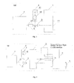
Fig. 1 is a structure diagram illustrating an electronic device provided by an embodiment of the present invention; -
Fig. 2 is a structure diagram illustrating a data transmission system provided by an embodiment of the present embodiment; -
Fig. 3 is a structure diagram illustrating an electronic device provided by an embodiment of the present invention; -
Fig. 4 is a structure diagram illustrating a data transmission system provided by an embodiment of the present invention; -
Fig. 5 is a structure diagram illustrating a data transmission system provided by an embodiment of the present invention; and -
Fig. 6 is a structure diagram illustrating a data transmission system provided by an embodiment of the present invention. - In order to make objects, the technical solutions and advantages of the present invention more clear, hereinafter, the embodiments of the present invention will be described in further detail in conjunction with the accompanying drawings.
- An embodiment of the present invention provides an electronic device (hereinafter referred to as a first electronic device 100). As shown in
Fig. 1 , the firstelectronic device 100 includes a micro universal serial bus (USB)interface 1, a central processing unit (CPU) 2 and adiode 3. - A pull-up circuit of an identity (ID)
pin 21 of the CPU is connected to a line between theID pin 21 of the CPU and anID pin 11 of the micro USB interface. Thediode 3 is provided in the line between theID pin 21 of the CPU and theID pin 11 of the micro USB interface, and is positioned between the pull-up circuit and theID pin 11 of the micro USB interface. A conducting direction of thediode 3 is a direction pointing from theID pin 21 of the CPU to theID pin 11 of the micro USB interface. - In an embodiment of the present invention, a first electronic device includes a micro USB interface, a CPU and a diode, wherein a pull-up circuit of an ID pin of the CPU is connected to a line between the ID pin of the CPU and an ID pin of the micro USB interface, the diode is provided in the line between the ID pin of the CPU and the ID pin of the micro USB interface, and is positioned between the pull-up circuit and the ID pin of the micro USB interface, and the diode has a conducting direction pointing from the ID pin of the CPU to the ID pin of the micro USB interface. Thus, if the first electronic device is connected to a device having a Type C USB interface via a conversion line and a CC1 pin and a VBUS are connected in the device having the Type C USB interface, then the diode may isolate a voltage of the VBUS from a voltage at the ID pin of the CPU. Consequently, the electronic device may be prevented from being damaged.
- An embodiment of the present invention provides a first
electronic device 100. As shown inFig. 1 , the firstelectronic device 100 includes amicro USB interface 1, a central processing unit (CPU) 2 and adiode 3. A pull-up circuit 4 of anID pin 21 of the CPU is connected to a line between theID pin 21 of the CPU and anID pin 11 of the micro USB interface. Thediode 3 is provided in the line between theID pin 21 of the CPU and theID pin 11 of the micro USB interface, and is positioned between the pull-up circuit 4 and theID pin 11 of the micro USB interface. Thediode 3 has a conducting direction pointing from theID pin 21 of the CPU to theID pin 11 of the micro USB interface. - The
diode 3 is an electronic device having characteristics of unidirectional conducting of current. In the present embodiment, thediode 3 may be a Schottky diode which has extremely strong forward (i.e., a conducting direction) conducting capability and reverse (i.e., a direction opposite to the conducting direction) protective capability. - In an embodiment, the first
electronic device 100 may be a device having a micro USB interface, such as a cellphone, a Tablet PC or the like. The firstelectronic device 100 is provided with themicro USB interface 1, and theID pin 11 of the micro USB interface is connected to theID pin 21 of the CPU. The pull-upcircuit 4 is provided for theID pin 21 of the CPU in the firstelectronic device 100 to pull up a voltage at theID pin 21 of the CPU. The pull-upcircuit 4 may be provided outside or inside of theCPU 2. A connection point of the pull-upcircuit 4 on the line between theID pin 11 of the micro USB interface and theID pin 21 of the CPU may be referred to as a point H, and thediode 3 may be provided between theID pin 11 of the micro USB interface and the point H. Thus, when the firstelectronic device 100 is connected to a device having a Type C USB interface via aconversion line 8 and a CC1 pin is connected to a VBUS via a resistor in the device having the Type C USB interface, thediode 3 may isolate a voltage of the VBUS from the voltage at theID pin 21 of the CPU, and the voltage at theID pin 21 of the CPU will not be influenced by the voltage of the VBUS, and will not be elevated to 5V. Thus, the firstelectronic device 100 will not be damaged. - Alternatively, a
first resistor 5 may be connected in series in the line between theID pin 11 of the micro USB interface and theID pin 21 of the CPU. - In an embodiment, the
first resistor 5 may be provided at an arbitrary position in the line between theID pin 11 of the micro USB interface and theID pin 21 of the CPU, or may be provided between thediode 3 and theID pin 21 of the CPU, or may be provided between thediode 3 and theID pin 11 of the micro USB interface. By providing thefirst resistor 5, theID pin 21 of the CPU may be further protected, and in a case where a voltage at theID pin 11 of the micro USB interface is relatively large and thediode 3 fails to block a reverse current, thefirst resistor 5 can further decrease the reverse current. - Optionally, as shown in
Fig. 1 , the pull-upcircuit 4 includes a pull-uppower supply 41 and asecond resistor 42. A voltage of the pull-up power supply 41 (referred to as a pull-up voltage) may be 1.8V. Thesecond resistor 42 may be connected in series between the pull-uppower supply 41 and the point H. - Optionally, a resistance value of the
second resistor 42 may be set to be greater than a lower limit of a preset resistance value. - In an embodiment, the
ID pin 21 of the CPU plays an important role in recognizing an external electronic device that is connected through themicro USB interface 1, that is, when an electronic device is connected, the connection of the electronic device is found by a change in the voltage at theID pin 21 of the CPU. For a type of device having a Type C USB interface, aCC1 pin 71 of the device is grounded via a resistor (hereinafter referred to as a third resistor 6) and, in order to increase the recognition rate when this type of device having the Type C USB interface is connected to themicro USB interface 1 of the firstelectronic device 100 via theconversion line 8, the resistance value of thesecond resistor 42 may be set such that the resistance value is greater than a specified lower limit of resistance value to guarantee the amplitude of changes in the voltage at theID pin 21 of the CPU when this type of device having the Type C USB interface is connected to the firstelectronic device 100, and thereby the recognition rate is increased. By setting the resistance value of thesecond resistor 42, when themicro USB interface 1 of the firstelectronic device 100 is not connected to other electronic devices, a voltage detected by theID pin 21 of the CPU is the voltage of the pull-uppower supply 41, for example 1.8V. When themicro USB interface 1 of the firstelectronic device 100 is connected to the above type of device having the Type C USB interface via theconversion line 8, as shown inFig. 2 , total resistance of thediode 3 and thethird resistor 6 and a resistance of thesecond resistor 42 form a voltage division to the pull-up voltage, and theID pin 21 of the CPU detects a voltage divided by the total resistance of thediode 3 and thethird resistor 6. If the resistance value of thesecond resistor 42 is large enough, the voltage detected by theID pin 21 of the CPU may be controlled within 30% of the pull-up voltage. Thus, the firstelectronic device 100 may detect the connection of the device having the Type C USB interface. Thereby, the lower limit of the resistance value may be set based on this principle. - Alternatively, as shown in
Fig. 3 , thefirst resistor 5 may be provided in a line between the pull-upcircuit 4 and theID pin 21 of the CPU. - In an embodiment, for the above type of device having the Type C USB interface whose CC1 pin is grounded via the resistor, in order to increase the recognition rate when this type of device having the Type C USB interface is connected to the
micro USB interface 1 of the firstelectronic device 100 via theconversion line 8, thefirst resistor 5 may be provided in the line between the pull-upcircuit 4 and the ID pin of the CPU, that is, provided in the line between the point H and the ID pin of the CPU. Thus, when themicro USB interface 1 of the firstelectronic device 100 is not connected to other electronic devices, a voltage detected by theID pin 21 of the CPU is the voltage of the pull-uppower supply 41 in the pull-upcircuit 4, for example 1.8V. When themicro USB interface 1 of the firstelectronic device 100 is connected to the above type of device having the Type C USB interface via theconversion line 8, as shown inFig. 4 , if thefirst resistor 5 is provided in the line between the point H and theID pin 21 of the CPU, theID pin 21 of the CPU detects a voltage divided by the total resistance of thediode 3 and thethird resistor 6. However, if thefirst resistor 5 is provided in the line between the point H and theID pin 11 of the micro USB interface, thefirst resistor 5 together with thediode 3 and thethird resistor 6 performs voltage division with thesecond resistor 42, and theID pin 21 of the CPU detects a voltage divided by total resistance of thediode 3, thefirst resistor 5 and thethird resistor 6. Thus, providing thefirst resistor 5 in the line between the point H and theID pin 21 of the CPU is more beneficial for decreasing the voltage detected by theID pin 21 of the CPU at this time. Thus, the firstelectronic device 100 more easily detects the connection of the device having the Type C USB interface. - In an embodiment of the present invention, a first electronic device includes a micro USB interface, a CPU and a diode. A pull-up circuit of an ID pin of the CPU is connected to a line between the ID pin of the CPU and an ID pin of the micro USB interface. The diode is provided in the line between the ID pin of the CPU and the ID pin of the micro USB interface, and is positioned between the pull-up circuit and the ID pin of the micro USB interface. The diode has a conducting direction pointing from the ID pin of the CPU to the ID pin of the micro USB interface. Thus, if the first electronic device is connected to a device having a Type C USB interface via a conversion line and a CC1 pin and a VBUS are connected in the device having the Type C USB interface, then the diode may isolate a voltage of the VBUS from a voltage at the ID pin of the CPU. Consequently, the electronic device may be prevented from being damaged.
- An embodiment of the present invention further provides a data transmission system. The data transmission system includes a second
electronic device 200 and the firstelectronic device 100 as described in above embodiments. The secondelectronic device 200 includes a TypeC USB interface 7, and the TypeC USB interface 7 of the secondelectronic device 200 is connected to themicro USB interface 1 of the firstelectronic device 100 via aconversion line 8. - The
conversion line 8 may be a conversion line providing conversion between the Type C USB interface and the micro USB interface. - In an embodiment, the second
electronic device 200 may be a device having a Type C USB interface, such as a U-disk, a USB speaker or the like. The secondelectronic device 200 may be any type of device having a Type C USB interface, it may be the above-described type of device having the Type C USB interface whoseCC1 pin 71 is connected to the VBUS via a resistor, as shown inFig. 5 , or may be the above-described type of device having the Type C USB interface whoseCC1 pin 71 is grounded via a resistor, as shown inFig. 6 . - Alternatively, as shown in
Figs. 5 and 6 , theCC1 pin 71 and aCC2 pin 72 of the Type C USB interface are connected to theID pin 11 of the micro USB interface via theconversion line 8; aVBUS pin 73 of the Type C USB interface is connected to aVBUS pin 12 of the micro USB interface via theconversion line 8; a D-pin 74 of the Type C USB interface is connected to a D-pin 13 of the micro USB interface via theconversion line 8; aD+ pin 75 of the Type C USB interface is connected to aD+ pin 14 of the micro USB interface via theconversion line 8; and aGND pin 76 of the Type C USB interface is connected to aGND pin 15 of the micro USB interface via theconversion line 8. - In an embodiment of the present invention, the first electronic device includes a micro USB interface, a CPU and a diode, wherein a pull-up circuit of an ID pin of the CPU is connected to a line between the ID pin of the CPU and an ID pin of the micro USB interface, the diode is provided in the line between the ID pin of the CPU and the ID pin of the micro USB interface, and is positioned between the pull-up circuit and the ID pin of the micro USB interface, and the diode has a conducting direction pointing from the ID pin of the CPU to the ID pin of the micro USB interface. Thus, if the first electronic device is connected to a device having a Type C USB interface via a
conversion line 8 and a CC1 pin and a VBUS are connected in the device having the Type C USB interface, then the diode may isolate a voltage of the VBUS from a voltage at the ID pin of the CPU. Consequently, the electronic device may be prevented from being damaged. - Those skilled in the art may understand, the whole or part of the steps in the above embodiments may be achieved by hardware, or may be achieved by relevant hardware which is instructed by using program. The program may be stored in a computer readable storage medium, and the storage medium may be an ROM, a magnetic disk or an optical disk, etc.
- The above contents are only the preferable embodiments of the present invention, which are not used to limit the present invention. Any changes, equal substitution and modifications, etc. within the spirit and principle of the present invention should be included in the protection scope of the present invention.
| 100 | First | 200 | Second |
| 1 | | 2 | |
| 3 | | 4 | Pull- |
| 5 | | 6 | |
| 7 | Type | 8 | |
| 11 | ID pin of the | 12 | VBUS pin of the micro USB interface |
| 13 | D- pin of the | 14 | D+ pin of the |
| 15 | GND pin of the | 21 | ID pin of the |
| 41 | Pull-up | 42 | |
| 71 | CC1 pin of the Type | 72 | CC2 pin of the Type |
| 73 | VBUS pin of the Type C USB interface | 74 | D- pin of the Type |
| 75 | D+ pin of the Type | 76 | GND pin of the Type C USB interface |
Claims (9)
- A first electronic device (100), characterized in that the first electronic device comprises a micro USB interface (1), a CPU (2) and a diode (3), wherein:a pull-up circuit (4) of an ID pin (21) of the CPU (2) is connected to a line between the ID pin (21) of the CPU and an ID pin (11) of the micro USB interface (1);the diode (3) is provided in the line between the ID pin (21) of the CPU (2) and the ID pin (11) of the micro USB interface (1), and is positioned between the pull-up circuit (4) and the ID pin (11) of the micro USB interface (1); andthe diode (3) has a conducting direction pointing from the ID pin (21) of the CPU (2) to the ID pin (11) of the micro USB interface (1).
- The first electronic device (100) according to claim 1, characterized in that a first resistor (5) is connected in series in the line between the ID pin (11) of the micro USB interface (1) and the ID pin (21) of the CPU (2).
- The first electronic device (100) according to claim 2, characterized in that the first resistor (5) is provided in a line between the pull-up circuit (4) and the ID pin (21) of the CPU (2).
- The first electronic device (100) according to any one of claims 1 to 3, characterized in that the pull-up circuit (4) comprises a pull-up power supply (41) and a second resistor (42).
- The first electronic device (100) according to claim 4, characterized in that a resistance value of the second resistor (42) is greater than a lower limit of a preset resistance value.
- The first electronic device according to claim 4 or 5, characterized in that a voltage of the pull-up power supply is 1.8V.
- The first electronic device according to any one of claims 1 to 6, characterized in that the diode (3) comprises a Schottky diode.
- A data transmission system, characterized in that the system comprises a second electronic device (200) and the first electronic device (100) according to any one of claims 1 to 7, the second electronic device (200) comprising a Type C USB interface (7), wherein:the Type C USB interface (7) of the second electronic device is connected to the micro USB interface (1) of the first electronic device via a conversion line (8).
- The data transmission system according to claim 8, characterized in that a CC1 pin (71) and a CC2 pin (72) of the Type C USB interface (7) are connected to the ID pin (11) of the micro USB interface (1) via the conversion line (8);
a power supply VBUS pin (73) of the Type C USB interface (7) is connected to a VBUS pin (12) of the micro USB interface (1) via the conversion line (8);
a D- pin (74) of the Type C USB interface (7) is connected to a D -pin (13) of the micro USB interface (1) via the conversion line (8);
a D+ pin (75) of the Type C USB interface (7) is connected to a D+ pin (14) of the micro USB interface (1) via the conversion line (8); and
a ground GND pin (76) of the Type C USB interface (7) is connected to a GND pin (15) of the micro USB interface (1) via the conversion line (8).
Applications Claiming Priority (1)
| Application Number | Priority Date | Filing Date | Title |
|---|---|---|---|
| CN201410851029.0A CN104615569A (en) | 2014-12-31 | 2014-12-31 | Electronic equipment and data transmission system |
Publications (2)
| Publication Number | Publication Date |
|---|---|
| EP3040872A1 true EP3040872A1 (en) | 2016-07-06 |
| EP3040872B1 EP3040872B1 (en) | 2018-07-04 |
Family
ID=53150021
Family Applications (1)
| Application Number | Title | Priority Date | Filing Date |
|---|---|---|---|
| EP15200802.5A Active EP3040872B1 (en) | 2014-12-31 | 2015-12-17 | Electronic device and data transmission system |
Country Status (8)
| Country | Link |
|---|---|
| EP (1) | EP3040872B1 (en) |
| JP (1) | JP6149173B2 (en) |
| KR (1) | KR20160092481A (en) |
| CN (1) | CN104615569A (en) |
| BR (1) | BR112015016821A2 (en) |
| MX (1) | MX353667B (en) |
| RU (1) | RU2625442C2 (en) |
| WO (1) | WO2016107033A1 (en) |
Cited By (1)
| Publication number | Priority date | Publication date | Assignee | Title |
|---|---|---|---|---|
| WO2021208291A1 (en) * | 2020-04-13 | 2021-10-21 | 深圳慧能泰半导体科技有限公司 | Charging cable, charging apparatus and charging cable protection system |
Families Citing this family (7)
| Publication number | Priority date | Publication date | Assignee | Title |
|---|---|---|---|---|
| CN104881391B (en) * | 2015-06-10 | 2017-09-19 | 赛尔康技术(深圳)有限公司 | An identification circuit for a USB Type-C interface |
| CN106887832B (en) * | 2015-12-16 | 2019-10-22 | 中兴通讯股份有限公司 | A circuit for protecting the USB interface of a terminal chip |
| CN105630724B (en) * | 2016-01-27 | 2017-03-15 | 深圳慧能泰半导体科技有限公司 | A kind of USB Type C system control circuits |
| CN106502939B (en) * | 2016-09-23 | 2020-01-10 | 北京小米移动软件有限公司 | USB adapter and data transmission equipment |
| CN106774596B (en) * | 2017-01-20 | 2019-04-23 | 深圳市金立通信设备有限公司 | A kind of electric power management circuit, electronic equipment and control method of electronic device |
| TWI662740B (en) * | 2018-01-09 | 2019-06-11 | 和碩聯合科技股份有限公司 | External antenna and wireless coummunication system |
| CN110825682B (en) * | 2019-11-05 | 2022-08-02 | 维沃移动通信有限公司 | USB control method and electronic equipment |
Citations (2)
| Publication number | Priority date | Publication date | Assignee | Title |
|---|---|---|---|---|
| US20080133802A1 (en) * | 2006-12-05 | 2008-06-05 | Nikon Corporation | Electronic device and interface system |
| US20080150512A1 (en) * | 2006-12-25 | 2008-06-26 | Nikon Corporation | Electronic device |
Family Cites Families (11)
| Publication number | Priority date | Publication date | Assignee | Title |
|---|---|---|---|---|
| US6813650B1 (en) * | 1999-10-26 | 2004-11-02 | International Business Machines Corporation | Multimode non-standard universal serial bus computer input device |
| TWI381276B (en) * | 2009-02-19 | 2013-01-01 | Inventec Corp | Computer apparatus |
| CN201638203U (en) * | 2010-04-30 | 2010-11-17 | 青岛海信移动通信技术股份有限公司 | Universal data line |
| CN201733438U (en) * | 2010-07-15 | 2011-02-02 | 广东欧珀移动通信有限公司 | A headphone plug-in detection circuit |
| CN102065160A (en) * | 2010-12-02 | 2011-05-18 | 惠州Tcl移动通信有限公司 | Circuit for being externally connected with loudspeaker by utilizing mobile phone |
| JP5742406B2 (en) * | 2011-04-08 | 2015-07-01 | 富士通株式会社 | Information processing apparatus, connection method, and program |
| CN102778918B (en) * | 2011-05-09 | 2016-08-24 | 国家电网公司 | Portable electron device |
| CN103138071A (en) * | 2011-12-02 | 2013-06-05 | 联想(北京)有限公司 | Universal serial bus (USB) interface socket |
| CN202798652U (en) * | 2012-06-27 | 2013-03-13 | 青岛海信移动通信技术股份有限公司 | Signal conversion circuit and interface switching equipment |
| CN103237189B (en) * | 2013-03-26 | 2016-01-13 | 小米科技有限责任公司 | Electronic equipment, MHL connector, MHL system and connector detection method |
| KR102048222B1 (en) * | 2013-05-21 | 2019-11-25 | 삼성전자주식회사 | Apparatus and method for recognizing an external device in a communication system |
-
2014
- 2014-12-31 CN CN201410851029.0A patent/CN104615569A/en active Pending
-
2015
- 2015-04-30 RU RU2015129478A patent/RU2625442C2/en active
- 2015-04-30 KR KR1020157017517A patent/KR20160092481A/en not_active Ceased
- 2015-04-30 JP JP2016567114A patent/JP6149173B2/en not_active Expired - Fee Related
- 2015-04-30 BR BR112015016821A patent/BR112015016821A2/en active Search and Examination
- 2015-04-30 MX MX2015009296A patent/MX353667B/en active IP Right Grant
- 2015-04-30 WO PCT/CN2015/077960 patent/WO2016107033A1/en not_active Ceased
- 2015-12-17 EP EP15200802.5A patent/EP3040872B1/en active Active
Patent Citations (2)
| Publication number | Priority date | Publication date | Assignee | Title |
|---|---|---|---|---|
| US20080133802A1 (en) * | 2006-12-05 | 2008-06-05 | Nikon Corporation | Electronic device and interface system |
| US20080150512A1 (en) * | 2006-12-25 | 2008-06-26 | Nikon Corporation | Electronic device |
Cited By (1)
| Publication number | Priority date | Publication date | Assignee | Title |
|---|---|---|---|---|
| WO2021208291A1 (en) * | 2020-04-13 | 2021-10-21 | 深圳慧能泰半导体科技有限公司 | Charging cable, charging apparatus and charging cable protection system |
Also Published As
| Publication number | Publication date |
|---|---|
| RU2625442C2 (en) | 2017-07-13 |
| JP2017505502A (en) | 2017-02-16 |
| RU2015129478A (en) | 2017-01-23 |
| MX2015009296A (en) | 2016-08-26 |
| MX353667B (en) | 2018-01-22 |
| KR20160092481A (en) | 2016-08-04 |
| WO2016107033A1 (en) | 2016-07-07 |
| CN104615569A (en) | 2015-05-13 |
| EP3040872B1 (en) | 2018-07-04 |
| JP6149173B2 (en) | 2017-06-14 |
| BR112015016821A2 (en) | 2017-07-11 |
Similar Documents
| Publication | Publication Date | Title |
|---|---|---|
| EP3040872B1 (en) | Electronic device and data transmission system | |
| KR102786096B1 (en) | USB Type-C/PD controller with integrated VBUS to CC short-circuit protection | |
| US9984030B2 (en) | Electronic device and data transmission system | |
| US20150002296A1 (en) | Connector identification through proximity sensing | |
| US10938200B2 (en) | Back power protection circuit | |
| CN105591355A (en) | USB-C control chip, USB-C control chip protection circuit, and USB-C system | |
| WO2015176621A1 (en) | Interface detection circuit, apparatus and method | |
| EP3242368A3 (en) | Over-voltage and ground fault protection for bus connectors | |
| US9606614B2 (en) | Load device and electronic device assembly with load device | |
| US9627901B2 (en) | Charging circuit | |
| US9722444B2 (en) | Electronic device and charging interface | |
| CN105006814B (en) | A kind of surge-proof method and system of two-way computing board | |
| US8351173B2 (en) | Power supply circuit | |
| EP3345097B1 (en) | Serial port pin voltages | |
| US20130271109A1 (en) | Electronic device with universal serial bus port | |
| CN108054722B (en) | Protective circuit | |
| US20160335213A1 (en) | Motherboard with multiple interfaces | |
| CN107610734B (en) | Power supply circuit of EEPROM and EEPROM | |
| AU2016200277B2 (en) | A power supply device and a system programming tool including the power supply device | |
| EP2637282A1 (en) | Discharge circuit | |
| CN107784347A (en) | The foldable USB flash disk of interface | |
| CN105207027A (en) | USB with external equipment protection circuit | |
| CN105204666A (en) | Mouse with wrist pad |
Legal Events
| Date | Code | Title | Description |
|---|---|---|---|
| PUAI | Public reference made under article 153(3) epc to a published international application that has entered the european phase |
Free format text: ORIGINAL CODE: 0009012 |
|
| AK | Designated contracting states |
Kind code of ref document: A1 Designated state(s): AL AT BE BG CH CY CZ DE DK EE ES FI FR GB GR HR HU IE IS IT LI LT LU LV MC MK MT NL NO PL PT RO RS SE SI SK SM TR |
|
| AX | Request for extension of the european patent |
Extension state: BA ME |
|
| 17P | Request for examination filed |
Effective date: 20161207 |
|
| RBV | Designated contracting states (corrected) |
Designated state(s): AL AT BE BG CH CY CZ DE DK EE ES FI FR GB GR HR HU IE IS IT LI LT LU LV MC MK MT NL NO PL PT RO RS SE SI SK SM TR |
|
| GRAP | Despatch of communication of intention to grant a patent |
Free format text: ORIGINAL CODE: EPIDOSNIGR1 |
|
| INTG | Intention to grant announced |
Effective date: 20180130 |
|
| GRAS | Grant fee paid |
Free format text: ORIGINAL CODE: EPIDOSNIGR3 |
|
| GRAA | (expected) grant |
Free format text: ORIGINAL CODE: 0009210 |
|
| AK | Designated contracting states |
Kind code of ref document: B1 Designated state(s): AL AT BE BG CH CY CZ DE DK EE ES FI FR GB GR HR HU IE IS IT LI LT LU LV MC MK MT NL NO PL PT RO RS SE SI SK SM TR |
|
| REG | Reference to a national code |
Ref country code: GB Ref legal event code: FG4D |
|
| REG | Reference to a national code |
Ref country code: CH Ref legal event code: EP |
|
| REG | Reference to a national code |
Ref country code: AT Ref legal event code: REF Ref document number: 1015261 Country of ref document: AT Kind code of ref document: T Effective date: 20180715 |
|
| REG | Reference to a national code |
Ref country code: IE Ref legal event code: FG4D |
|
| REG | Reference to a national code |
Ref country code: DE Ref legal event code: R096 Ref document number: 602015012969 Country of ref document: DE |
|
| REG | Reference to a national code |
Ref country code: NL Ref legal event code: MP Effective date: 20180704 |
|
| REG | Reference to a national code |
Ref country code: LT Ref legal event code: MG4D |
|
| REG | Reference to a national code |
Ref country code: AT Ref legal event code: MK05 Ref document number: 1015261 Country of ref document: AT Kind code of ref document: T Effective date: 20180704 |
|
| PG25 | Lapsed in a contracting state [announced via postgrant information from national office to epo] |
Ref country code: NL Free format text: LAPSE BECAUSE OF FAILURE TO SUBMIT A TRANSLATION OF THE DESCRIPTION OR TO PAY THE FEE WITHIN THE PRESCRIBED TIME-LIMIT Effective date: 20180704 |
|
| PG25 | Lapsed in a contracting state [announced via postgrant information from national office to epo] |
Ref country code: PL Free format text: LAPSE BECAUSE OF FAILURE TO SUBMIT A TRANSLATION OF THE DESCRIPTION OR TO PAY THE FEE WITHIN THE PRESCRIBED TIME-LIMIT Effective date: 20180704 Ref country code: RS Free format text: LAPSE BECAUSE OF FAILURE TO SUBMIT A TRANSLATION OF THE DESCRIPTION OR TO PAY THE FEE WITHIN THE PRESCRIBED TIME-LIMIT Effective date: 20180704 Ref country code: IS Free format text: LAPSE BECAUSE OF FAILURE TO SUBMIT A TRANSLATION OF THE DESCRIPTION OR TO PAY THE FEE WITHIN THE PRESCRIBED TIME-LIMIT Effective date: 20181104 Ref country code: LT Free format text: LAPSE BECAUSE OF FAILURE TO SUBMIT A TRANSLATION OF THE DESCRIPTION OR TO PAY THE FEE WITHIN THE PRESCRIBED TIME-LIMIT Effective date: 20180704 Ref country code: BG Free format text: LAPSE BECAUSE OF FAILURE TO SUBMIT A TRANSLATION OF THE DESCRIPTION OR TO PAY THE FEE WITHIN THE PRESCRIBED TIME-LIMIT Effective date: 20181004 Ref country code: SE Free format text: LAPSE BECAUSE OF FAILURE TO SUBMIT A TRANSLATION OF THE DESCRIPTION OR TO PAY THE FEE WITHIN THE PRESCRIBED TIME-LIMIT Effective date: 20180704 Ref country code: CZ Free format text: LAPSE BECAUSE OF FAILURE TO SUBMIT A TRANSLATION OF THE DESCRIPTION OR TO PAY THE FEE WITHIN THE PRESCRIBED TIME-LIMIT Effective date: 20180704 Ref country code: GR Free format text: LAPSE BECAUSE OF FAILURE TO SUBMIT A TRANSLATION OF THE DESCRIPTION OR TO PAY THE FEE WITHIN THE PRESCRIBED TIME-LIMIT Effective date: 20181005 Ref country code: FI Free format text: LAPSE BECAUSE OF FAILURE TO SUBMIT A TRANSLATION OF THE DESCRIPTION OR TO PAY THE FEE WITHIN THE PRESCRIBED TIME-LIMIT Effective date: 20180704 Ref country code: AT Free format text: LAPSE BECAUSE OF FAILURE TO SUBMIT A TRANSLATION OF THE DESCRIPTION OR TO PAY THE FEE WITHIN THE PRESCRIBED TIME-LIMIT Effective date: 20180704 Ref country code: NO Free format text: LAPSE BECAUSE OF FAILURE TO SUBMIT A TRANSLATION OF THE DESCRIPTION OR TO PAY THE FEE WITHIN THE PRESCRIBED TIME-LIMIT Effective date: 20181004 |
|
| PG25 | Lapsed in a contracting state [announced via postgrant information from national office to epo] |
Ref country code: HR Free format text: LAPSE BECAUSE OF FAILURE TO SUBMIT A TRANSLATION OF THE DESCRIPTION OR TO PAY THE FEE WITHIN THE PRESCRIBED TIME-LIMIT Effective date: 20180704 Ref country code: ES Free format text: LAPSE BECAUSE OF FAILURE TO SUBMIT A TRANSLATION OF THE DESCRIPTION OR TO PAY THE FEE WITHIN THE PRESCRIBED TIME-LIMIT Effective date: 20180704 Ref country code: LV Free format text: LAPSE BECAUSE OF FAILURE TO SUBMIT A TRANSLATION OF THE DESCRIPTION OR TO PAY THE FEE WITHIN THE PRESCRIBED TIME-LIMIT Effective date: 20180704 Ref country code: AL Free format text: LAPSE BECAUSE OF FAILURE TO SUBMIT A TRANSLATION OF THE DESCRIPTION OR TO PAY THE FEE WITHIN THE PRESCRIBED TIME-LIMIT Effective date: 20180704 |
|
| REG | Reference to a national code |
Ref country code: DE Ref legal event code: R097 Ref document number: 602015012969 Country of ref document: DE |
|
| PG25 | Lapsed in a contracting state [announced via postgrant information from national office to epo] |
Ref country code: IT Free format text: LAPSE BECAUSE OF FAILURE TO SUBMIT A TRANSLATION OF THE DESCRIPTION OR TO PAY THE FEE WITHIN THE PRESCRIBED TIME-LIMIT Effective date: 20180704 Ref country code: RO Free format text: LAPSE BECAUSE OF FAILURE TO SUBMIT A TRANSLATION OF THE DESCRIPTION OR TO PAY THE FEE WITHIN THE PRESCRIBED TIME-LIMIT Effective date: 20180704 Ref country code: EE Free format text: LAPSE BECAUSE OF FAILURE TO SUBMIT A TRANSLATION OF THE DESCRIPTION OR TO PAY THE FEE WITHIN THE PRESCRIBED TIME-LIMIT Effective date: 20180704 |
|
| PLBE | No opposition filed within time limit |
Free format text: ORIGINAL CODE: 0009261 |
|
| STAA | Information on the status of an ep patent application or granted ep patent |
Free format text: STATUS: NO OPPOSITION FILED WITHIN TIME LIMIT |
|
| PG25 | Lapsed in a contracting state [announced via postgrant information from national office to epo] |
Ref country code: SK Free format text: LAPSE BECAUSE OF FAILURE TO SUBMIT A TRANSLATION OF THE DESCRIPTION OR TO PAY THE FEE WITHIN THE PRESCRIBED TIME-LIMIT Effective date: 20180704 Ref country code: DK Free format text: LAPSE BECAUSE OF FAILURE TO SUBMIT A TRANSLATION OF THE DESCRIPTION OR TO PAY THE FEE WITHIN THE PRESCRIBED TIME-LIMIT Effective date: 20180704 Ref country code: SM Free format text: LAPSE BECAUSE OF FAILURE TO SUBMIT A TRANSLATION OF THE DESCRIPTION OR TO PAY THE FEE WITHIN THE PRESCRIBED TIME-LIMIT Effective date: 20180704 |
|
| 26N | No opposition filed |
Effective date: 20190405 |
|
| REG | Reference to a national code |
Ref country code: CH Ref legal event code: PL |
|
| PG25 | Lapsed in a contracting state [announced via postgrant information from national office to epo] |
Ref country code: SI Free format text: LAPSE BECAUSE OF FAILURE TO SUBMIT A TRANSLATION OF THE DESCRIPTION OR TO PAY THE FEE WITHIN THE PRESCRIBED TIME-LIMIT Effective date: 20180704 Ref country code: LU Free format text: LAPSE BECAUSE OF NON-PAYMENT OF DUE FEES Effective date: 20181217 Ref country code: MC Free format text: LAPSE BECAUSE OF FAILURE TO SUBMIT A TRANSLATION OF THE DESCRIPTION OR TO PAY THE FEE WITHIN THE PRESCRIBED TIME-LIMIT Effective date: 20180704 |
|
| REG | Reference to a national code |
Ref country code: IE Ref legal event code: MM4A |
|
| REG | Reference to a national code |
Ref country code: BE Ref legal event code: MM Effective date: 20181231 |
|
| PG25 | Lapsed in a contracting state [announced via postgrant information from national office to epo] |
Ref country code: IE Free format text: LAPSE BECAUSE OF NON-PAYMENT OF DUE FEES Effective date: 20181217 |
|
| PG25 | Lapsed in a contracting state [announced via postgrant information from national office to epo] |
Ref country code: BE Free format text: LAPSE BECAUSE OF NON-PAYMENT OF DUE FEES Effective date: 20181231 |
|
| PG25 | Lapsed in a contracting state [announced via postgrant information from national office to epo] |
Ref country code: CH Free format text: LAPSE BECAUSE OF NON-PAYMENT OF DUE FEES Effective date: 20181231 Ref country code: LI Free format text: LAPSE BECAUSE OF NON-PAYMENT OF DUE FEES Effective date: 20181231 |
|
| PG25 | Lapsed in a contracting state [announced via postgrant information from national office to epo] |
Ref country code: MT Free format text: LAPSE BECAUSE OF NON-PAYMENT OF DUE FEES Effective date: 20181217 |
|
| PG25 | Lapsed in a contracting state [announced via postgrant information from national office to epo] |
Ref country code: TR Free format text: LAPSE BECAUSE OF FAILURE TO SUBMIT A TRANSLATION OF THE DESCRIPTION OR TO PAY THE FEE WITHIN THE PRESCRIBED TIME-LIMIT Effective date: 20180704 |
|
| PG25 | Lapsed in a contracting state [announced via postgrant information from national office to epo] |
Ref country code: PT Free format text: LAPSE BECAUSE OF FAILURE TO SUBMIT A TRANSLATION OF THE DESCRIPTION OR TO PAY THE FEE WITHIN THE PRESCRIBED TIME-LIMIT Effective date: 20180704 |
|
| PG25 | Lapsed in a contracting state [announced via postgrant information from national office to epo] |
Ref country code: MK Free format text: LAPSE BECAUSE OF NON-PAYMENT OF DUE FEES Effective date: 20180704 Ref country code: HU Free format text: LAPSE BECAUSE OF FAILURE TO SUBMIT A TRANSLATION OF THE DESCRIPTION OR TO PAY THE FEE WITHIN THE PRESCRIBED TIME-LIMIT; INVALID AB INITIO Effective date: 20151217 Ref country code: CY Free format text: LAPSE BECAUSE OF FAILURE TO SUBMIT A TRANSLATION OF THE DESCRIPTION OR TO PAY THE FEE WITHIN THE PRESCRIBED TIME-LIMIT Effective date: 20180704 |
|
| REG | Reference to a national code |
Ref country code: DE Ref legal event code: R082 Ref document number: 602015012969 Country of ref document: DE Representative=s name: CBDL PATENTANWAELTE GBR, DE Ref country code: DE Ref legal event code: R082 Ref document number: 602015012969 Country of ref document: DE Representative=s name: CBDL PATENTANWAELTE EGBR, DE |
|
| P01 | Opt-out of the competence of the unified patent court (upc) registered |
Effective date: 20230523 |
|
| PGFP | Annual fee paid to national office [announced via postgrant information from national office to epo] |
Ref country code: GB Payment date: 20231220 Year of fee payment: 9 |
|
| PGFP | Annual fee paid to national office [announced via postgrant information from national office to epo] |
Ref country code: FR Payment date: 20231221 Year of fee payment: 9 |
|
| GBPC | Gb: european patent ceased through non-payment of renewal fee |
Effective date: 20241217 |
|
| PG25 | Lapsed in a contracting state [announced via postgrant information from national office to epo] |
Ref country code: GB Free format text: LAPSE BECAUSE OF NON-PAYMENT OF DUE FEES Effective date: 20241217 |
|
| PG25 | Lapsed in a contracting state [announced via postgrant information from national office to epo] |
Ref country code: FR Free format text: LAPSE BECAUSE OF NON-PAYMENT OF DUE FEES Effective date: 20241231 |
|
| PGFP | Annual fee paid to national office [announced via postgrant information from national office to epo] |
Ref country code: DE Payment date: 20251212 Year of fee payment: 11 |