EP3040824A1 - Touch sensor integrated type display device - Google Patents
Touch sensor integrated type display device Download PDFInfo
- Publication number
- EP3040824A1 EP3040824A1 EP15198202.2A EP15198202A EP3040824A1 EP 3040824 A1 EP3040824 A1 EP 3040824A1 EP 15198202 A EP15198202 A EP 15198202A EP 3040824 A1 EP3040824 A1 EP 3040824A1
- Authority
- EP
- European Patent Office
- Prior art keywords
- voltage
- data
- driving block
- switch
- touch
- Prior art date
- Legal status (The legal status is an assumption and is not a legal conclusion. Google has not performed a legal analysis and makes no representation as to the accuracy of the status listed.)
- Granted
Links
- 239000004973 liquid crystal related substance Substances 0.000 description 11
- 238000011084 recovery Methods 0.000 description 11
- 239000000758 substrate Substances 0.000 description 8
- 210000002858 crystal cell Anatomy 0.000 description 7
- 238000010586 diagram Methods 0.000 description 5
- 230000004044 response Effects 0.000 description 4
- 239000004020 conductor Substances 0.000 description 3
- 238000001514 detection method Methods 0.000 description 3
- 238000012986 modification Methods 0.000 description 3
- 230000004048 modification Effects 0.000 description 3
- 230000001360 synchronised effect Effects 0.000 description 3
- 238000004891 communication Methods 0.000 description 2
- 239000010949 copper Substances 0.000 description 2
- 238000009413 insulation Methods 0.000 description 2
- 239000011159 matrix material Substances 0.000 description 2
- 229910052751 metal Inorganic materials 0.000 description 2
- 239000002184 metal Substances 0.000 description 2
- 238000000034 method Methods 0.000 description 2
- VYZAMTAEIAYCRO-UHFFFAOYSA-N Chromium Chemical compound [Cr] VYZAMTAEIAYCRO-UHFFFAOYSA-N 0.000 description 1
- RYGMFSIKBFXOCR-UHFFFAOYSA-N Copper Chemical compound [Cu] RYGMFSIKBFXOCR-UHFFFAOYSA-N 0.000 description 1
- ZOKXTWBITQBERF-UHFFFAOYSA-N Molybdenum Chemical compound [Mo] ZOKXTWBITQBERF-UHFFFAOYSA-N 0.000 description 1
- 241000699670 Mus sp. Species 0.000 description 1
- BQCADISMDOOEFD-UHFFFAOYSA-N Silver Chemical compound [Ag] BQCADISMDOOEFD-UHFFFAOYSA-N 0.000 description 1
- 229910052782 aluminium Inorganic materials 0.000 description 1
- XAGFODPZIPBFFR-UHFFFAOYSA-N aluminium Chemical compound [Al] XAGFODPZIPBFFR-UHFFFAOYSA-N 0.000 description 1
- 230000008901 benefit Effects 0.000 description 1
- 230000005540 biological transmission Effects 0.000 description 1
- 239000003990 capacitor Substances 0.000 description 1
- 210000004027 cell Anatomy 0.000 description 1
- 230000008859 change Effects 0.000 description 1
- 229910052802 copper Inorganic materials 0.000 description 1
- 230000000694 effects Effects 0.000 description 1
- 230000005684 electric field Effects 0.000 description 1
- 230000005611 electricity Effects 0.000 description 1
- 238000005516 engineering process Methods 0.000 description 1
- 239000010408 film Substances 0.000 description 1
- AMGQUBHHOARCQH-UHFFFAOYSA-N indium;oxotin Chemical compound [In].[Sn]=O AMGQUBHHOARCQH-UHFFFAOYSA-N 0.000 description 1
- 229910052750 molybdenum Inorganic materials 0.000 description 1
- 239000011733 molybdenum Substances 0.000 description 1
- 230000008569 process Effects 0.000 description 1
- 230000000630 rising effect Effects 0.000 description 1
- 238000005070 sampling Methods 0.000 description 1
- 230000035945 sensitivity Effects 0.000 description 1
- 229910052709 silver Inorganic materials 0.000 description 1
- 239000004332 silver Substances 0.000 description 1
- 125000006850 spacer group Chemical group 0.000 description 1
- 239000010409 thin film Substances 0.000 description 1
- 230000007704 transition Effects 0.000 description 1
- 239000002699 waste material Substances 0.000 description 1
Images


Classifications
-
- G—PHYSICS
- G09—EDUCATION; CRYPTOGRAPHY; DISPLAY; ADVERTISING; SEALS
- G09G—ARRANGEMENTS OR CIRCUITS FOR CONTROL OF INDICATING DEVICES USING STATIC MEANS TO PRESENT VARIABLE INFORMATION
- G09G3/00—Control arrangements or circuits, of interest only in connection with visual indicators other than cathode-ray tubes
- G09G3/20—Control arrangements or circuits, of interest only in connection with visual indicators other than cathode-ray tubes for presentation of an assembly of a number of characters, e.g. a page, by composing the assembly by combination of individual elements arranged in a matrix no fixed position being assigned to or needed to be assigned to the individual characters or partial characters
- G09G3/34—Control arrangements or circuits, of interest only in connection with visual indicators other than cathode-ray tubes for presentation of an assembly of a number of characters, e.g. a page, by composing the assembly by combination of individual elements arranged in a matrix no fixed position being assigned to or needed to be assigned to the individual characters or partial characters by control of light from an independent source
- G09G3/36—Control arrangements or circuits, of interest only in connection with visual indicators other than cathode-ray tubes for presentation of an assembly of a number of characters, e.g. a page, by composing the assembly by combination of individual elements arranged in a matrix no fixed position being assigned to or needed to be assigned to the individual characters or partial characters by control of light from an independent source using liquid crystals
-
- G—PHYSICS
- G06—COMPUTING; CALCULATING OR COUNTING
- G06F—ELECTRIC DIGITAL DATA PROCESSING
- G06F3/00—Input arrangements for transferring data to be processed into a form capable of being handled by the computer; Output arrangements for transferring data from processing unit to output unit, e.g. interface arrangements
- G06F3/01—Input arrangements or combined input and output arrangements for interaction between user and computer
- G06F3/03—Arrangements for converting the position or the displacement of a member into a coded form
- G06F3/041—Digitisers, e.g. for touch screens or touch pads, characterised by the transducing means
- G06F3/0412—Digitisers structurally integrated in a display
-
- G—PHYSICS
- G02—OPTICS
- G02F—OPTICAL DEVICES OR ARRANGEMENTS FOR THE CONTROL OF LIGHT BY MODIFICATION OF THE OPTICAL PROPERTIES OF THE MEDIA OF THE ELEMENTS INVOLVED THEREIN; NON-LINEAR OPTICS; FREQUENCY-CHANGING OF LIGHT; OPTICAL LOGIC ELEMENTS; OPTICAL ANALOGUE/DIGITAL CONVERTERS
- G02F1/00—Devices or arrangements for the control of the intensity, colour, phase, polarisation or direction of light arriving from an independent light source, e.g. switching, gating or modulating; Non-linear optics
- G02F1/01—Devices or arrangements for the control of the intensity, colour, phase, polarisation or direction of light arriving from an independent light source, e.g. switching, gating or modulating; Non-linear optics for the control of the intensity, phase, polarisation or colour
- G02F1/13—Devices or arrangements for the control of the intensity, colour, phase, polarisation or direction of light arriving from an independent light source, e.g. switching, gating or modulating; Non-linear optics for the control of the intensity, phase, polarisation or colour based on liquid crystals, e.g. single liquid crystal display cells
- G02F1/133—Constructional arrangements; Operation of liquid crystal cells; Circuit arrangements
- G02F1/1333—Constructional arrangements; Manufacturing methods
- G02F1/13338—Input devices, e.g. touch panels
-
- G—PHYSICS
- G06—COMPUTING; CALCULATING OR COUNTING
- G06F—ELECTRIC DIGITAL DATA PROCESSING
- G06F1/00—Details not covered by groups G06F3/00 - G06F13/00 and G06F21/00
- G06F1/26—Power supply means, e.g. regulation thereof
- G06F1/32—Means for saving power
- G06F1/3203—Power management, i.e. event-based initiation of a power-saving mode
- G06F1/3206—Monitoring of events, devices or parameters that trigger a change in power modality
-
- G—PHYSICS
- G06—COMPUTING; CALCULATING OR COUNTING
- G06F—ELECTRIC DIGITAL DATA PROCESSING
- G06F1/00—Details not covered by groups G06F3/00 - G06F13/00 and G06F21/00
- G06F1/26—Power supply means, e.g. regulation thereof
- G06F1/32—Means for saving power
- G06F1/3203—Power management, i.e. event-based initiation of a power-saving mode
- G06F1/3234—Power saving characterised by the action undertaken
- G06F1/325—Power saving in peripheral device
- G06F1/3262—Power saving in digitizer or tablet
-
- G—PHYSICS
- G06—COMPUTING; CALCULATING OR COUNTING
- G06F—ELECTRIC DIGITAL DATA PROCESSING
- G06F1/00—Details not covered by groups G06F3/00 - G06F13/00 and G06F21/00
- G06F1/26—Power supply means, e.g. regulation thereof
- G06F1/32—Means for saving power
- G06F1/3203—Power management, i.e. event-based initiation of a power-saving mode
- G06F1/3234—Power saving characterised by the action undertaken
- G06F1/325—Power saving in peripheral device
- G06F1/3265—Power saving in display device
-
- G—PHYSICS
- G06—COMPUTING; CALCULATING OR COUNTING
- G06F—ELECTRIC DIGITAL DATA PROCESSING
- G06F1/00—Details not covered by groups G06F3/00 - G06F13/00 and G06F21/00
- G06F1/26—Power supply means, e.g. regulation thereof
- G06F1/32—Means for saving power
- G06F1/3203—Power management, i.e. event-based initiation of a power-saving mode
- G06F1/3234—Power saving characterised by the action undertaken
- G06F1/3287—Power saving characterised by the action undertaken by switching off individual functional units in the computer system
-
- G—PHYSICS
- G06—COMPUTING; CALCULATING OR COUNTING
- G06F—ELECTRIC DIGITAL DATA PROCESSING
- G06F3/00—Input arrangements for transferring data to be processed into a form capable of being handled by the computer; Output arrangements for transferring data from processing unit to output unit, e.g. interface arrangements
- G06F3/01—Input arrangements or combined input and output arrangements for interaction between user and computer
- G06F3/03—Arrangements for converting the position or the displacement of a member into a coded form
- G06F3/041—Digitisers, e.g. for touch screens or touch pads, characterised by the transducing means
- G06F3/0416—Control or interface arrangements specially adapted for digitisers
- G06F3/04166—Details of scanning methods, e.g. sampling time, grouping of sub areas or time sharing with display driving
-
- G—PHYSICS
- G06—COMPUTING; CALCULATING OR COUNTING
- G06F—ELECTRIC DIGITAL DATA PROCESSING
- G06F3/00—Input arrangements for transferring data to be processed into a form capable of being handled by the computer; Output arrangements for transferring data from processing unit to output unit, e.g. interface arrangements
- G06F3/01—Input arrangements or combined input and output arrangements for interaction between user and computer
- G06F3/03—Arrangements for converting the position or the displacement of a member into a coded form
- G06F3/041—Digitisers, e.g. for touch screens or touch pads, characterised by the transducing means
- G06F3/0416—Control or interface arrangements specially adapted for digitisers
- G06F3/0418—Control or interface arrangements specially adapted for digitisers for error correction or compensation, e.g. based on parallax, calibration or alignment
- G06F3/04184—Synchronisation with the driving of the display or the backlighting unit to avoid interferences generated internally
-
- G—PHYSICS
- G06—COMPUTING; CALCULATING OR COUNTING
- G06F—ELECTRIC DIGITAL DATA PROCESSING
- G06F3/00—Input arrangements for transferring data to be processed into a form capable of being handled by the computer; Output arrangements for transferring data from processing unit to output unit, e.g. interface arrangements
- G06F3/01—Input arrangements or combined input and output arrangements for interaction between user and computer
- G06F3/03—Arrangements for converting the position or the displacement of a member into a coded form
- G06F3/041—Digitisers, e.g. for touch screens or touch pads, characterised by the transducing means
- G06F3/044—Digitisers, e.g. for touch screens or touch pads, characterised by the transducing means by capacitive means
- G06F3/0446—Digitisers, e.g. for touch screens or touch pads, characterised by the transducing means by capacitive means using a grid-like structure of electrodes in at least two directions, e.g. using row and column electrodes
-
- G—PHYSICS
- G09—EDUCATION; CRYPTOGRAPHY; DISPLAY; ADVERTISING; SEALS
- G09G—ARRANGEMENTS OR CIRCUITS FOR CONTROL OF INDICATING DEVICES USING STATIC MEANS TO PRESENT VARIABLE INFORMATION
- G09G3/00—Control arrangements or circuits, of interest only in connection with visual indicators other than cathode-ray tubes
- G09G3/20—Control arrangements or circuits, of interest only in connection with visual indicators other than cathode-ray tubes for presentation of an assembly of a number of characters, e.g. a page, by composing the assembly by combination of individual elements arranged in a matrix no fixed position being assigned to or needed to be assigned to the individual characters or partial characters
- G09G3/34—Control arrangements or circuits, of interest only in connection with visual indicators other than cathode-ray tubes for presentation of an assembly of a number of characters, e.g. a page, by composing the assembly by combination of individual elements arranged in a matrix no fixed position being assigned to or needed to be assigned to the individual characters or partial characters by control of light from an independent source
- G09G3/36—Control arrangements or circuits, of interest only in connection with visual indicators other than cathode-ray tubes for presentation of an assembly of a number of characters, e.g. a page, by composing the assembly by combination of individual elements arranged in a matrix no fixed position being assigned to or needed to be assigned to the individual characters or partial characters by control of light from an independent source using liquid crystals
- G09G3/3603—Control arrangements or circuits, of interest only in connection with visual indicators other than cathode-ray tubes for presentation of an assembly of a number of characters, e.g. a page, by composing the assembly by combination of individual elements arranged in a matrix no fixed position being assigned to or needed to be assigned to the individual characters or partial characters by control of light from an independent source using liquid crystals with thermally addressed liquid crystals
-
- G—PHYSICS
- G09—EDUCATION; CRYPTOGRAPHY; DISPLAY; ADVERTISING; SEALS
- G09G—ARRANGEMENTS OR CIRCUITS FOR CONTROL OF INDICATING DEVICES USING STATIC MEANS TO PRESENT VARIABLE INFORMATION
- G09G3/00—Control arrangements or circuits, of interest only in connection with visual indicators other than cathode-ray tubes
- G09G3/20—Control arrangements or circuits, of interest only in connection with visual indicators other than cathode-ray tubes for presentation of an assembly of a number of characters, e.g. a page, by composing the assembly by combination of individual elements arranged in a matrix no fixed position being assigned to or needed to be assigned to the individual characters or partial characters
- G09G3/34—Control arrangements or circuits, of interest only in connection with visual indicators other than cathode-ray tubes for presentation of an assembly of a number of characters, e.g. a page, by composing the assembly by combination of individual elements arranged in a matrix no fixed position being assigned to or needed to be assigned to the individual characters or partial characters by control of light from an independent source
- G09G3/36—Control arrangements or circuits, of interest only in connection with visual indicators other than cathode-ray tubes for presentation of an assembly of a number of characters, e.g. a page, by composing the assembly by combination of individual elements arranged in a matrix no fixed position being assigned to or needed to be assigned to the individual characters or partial characters by control of light from an independent source using liquid crystals
- G09G3/3611—Control of matrices with row and column drivers
- G09G3/3648—Control of matrices with row and column drivers using an active matrix
-
- G—PHYSICS
- G09—EDUCATION; CRYPTOGRAPHY; DISPLAY; ADVERTISING; SEALS
- G09G—ARRANGEMENTS OR CIRCUITS FOR CONTROL OF INDICATING DEVICES USING STATIC MEANS TO PRESENT VARIABLE INFORMATION
- G09G3/00—Control arrangements or circuits, of interest only in connection with visual indicators other than cathode-ray tubes
- G09G3/20—Control arrangements or circuits, of interest only in connection with visual indicators other than cathode-ray tubes for presentation of an assembly of a number of characters, e.g. a page, by composing the assembly by combination of individual elements arranged in a matrix no fixed position being assigned to or needed to be assigned to the individual characters or partial characters
- G09G3/34—Control arrangements or circuits, of interest only in connection with visual indicators other than cathode-ray tubes for presentation of an assembly of a number of characters, e.g. a page, by composing the assembly by combination of individual elements arranged in a matrix no fixed position being assigned to or needed to be assigned to the individual characters or partial characters by control of light from an independent source
- G09G3/36—Control arrangements or circuits, of interest only in connection with visual indicators other than cathode-ray tubes for presentation of an assembly of a number of characters, e.g. a page, by composing the assembly by combination of individual elements arranged in a matrix no fixed position being assigned to or needed to be assigned to the individual characters or partial characters by control of light from an independent source using liquid crystals
- G09G3/3611—Control of matrices with row and column drivers
- G09G3/3685—Details of drivers for data electrodes
- G09G3/3688—Details of drivers for data electrodes suitable for active matrices only
-
- G—PHYSICS
- G09—EDUCATION; CRYPTOGRAPHY; DISPLAY; ADVERTISING; SEALS
- G09G—ARRANGEMENTS OR CIRCUITS FOR CONTROL OF INDICATING DEVICES USING STATIC MEANS TO PRESENT VARIABLE INFORMATION
- G09G2310/00—Command of the display device
- G09G2310/08—Details of timing specific for flat panels, other than clock recovery
-
- G—PHYSICS
- G09—EDUCATION; CRYPTOGRAPHY; DISPLAY; ADVERTISING; SEALS
- G09G—ARRANGEMENTS OR CIRCUITS FOR CONTROL OF INDICATING DEVICES USING STATIC MEANS TO PRESENT VARIABLE INFORMATION
- G09G2330/00—Aspects of power supply; Aspects of display protection and defect management
- G09G2330/02—Details of power systems and of start or stop of display operation
- G09G2330/021—Power management, e.g. power saving
-
- Y—GENERAL TAGGING OF NEW TECHNOLOGICAL DEVELOPMENTS; GENERAL TAGGING OF CROSS-SECTIONAL TECHNOLOGIES SPANNING OVER SEVERAL SECTIONS OF THE IPC; TECHNICAL SUBJECTS COVERED BY FORMER USPC CROSS-REFERENCE ART COLLECTIONS [XRACs] AND DIGESTS
- Y02—TECHNOLOGIES OR APPLICATIONS FOR MITIGATION OR ADAPTATION AGAINST CLIMATE CHANGE
- Y02D—CLIMATE CHANGE MITIGATION TECHNOLOGIES IN INFORMATION AND COMMUNICATION TECHNOLOGIES [ICT], I.E. INFORMATION AND COMMUNICATION TECHNOLOGIES AIMING AT THE REDUCTION OF THEIR OWN ENERGY USE
- Y02D10/00—Energy efficient computing, e.g. low power processors, power management or thermal management
-
- Y—GENERAL TAGGING OF NEW TECHNOLOGICAL DEVELOPMENTS; GENERAL TAGGING OF CROSS-SECTIONAL TECHNOLOGIES SPANNING OVER SEVERAL SECTIONS OF THE IPC; TECHNICAL SUBJECTS COVERED BY FORMER USPC CROSS-REFERENCE ART COLLECTIONS [XRACs] AND DIGESTS
- Y02—TECHNOLOGIES OR APPLICATIONS FOR MITIGATION OR ADAPTATION AGAINST CLIMATE CHANGE
- Y02D—CLIMATE CHANGE MITIGATION TECHNOLOGIES IN INFORMATION AND COMMUNICATION TECHNOLOGIES [ICT], I.E. INFORMATION AND COMMUNICATION TECHNOLOGIES AIMING AT THE REDUCTION OF THEIR OWN ENERGY USE
- Y02D30/00—Reducing energy consumption in communication networks
- Y02D30/50—Reducing energy consumption in communication networks in wire-line communication networks, e.g. low power modes or reduced link rate
Definitions
- This document relates to a touch sensor integrated type display device.
- UI User interfaces
- Typical examples of the user interfaces include keypads, keyboards, mice, on-screen displays (OSD), and remote controllers with an infrared communication capability or radio frequency (RF) communication capability.
- OSD on-screen displays
- RF radio frequency
- the user interface technology is continuing make progress toward increasing user sensitivity and ease of operation.
- user interfaces have been evolving into touch UI, voice recognition UI, 3D UI, etc.
- touch UIs for portable information devices is becoming essential, and moreover, the touch UIs are expanding its range of application to home appliances.
- Capacitive touchscreens can be used in a variety of applications since they have higher durability and better contrast than conventional resistive touchscreens and allow for multi-touch sensing and proximity-touch sensing.
- in-cell type touch screen integrated-type display devices incorporating elements constituting a touchscreen to make portable terminals such as smartphones, tablet PCs, etc slimmer.
- in-cell touchscreen integrated type display devices common electrodes for display are segmented into those for a plurality of touch driving periods and those for a plurality of touch sensing periods so that mutual capacitance occurs between the touch driving periods and the touch sensing periods. Therefore, the in-cell touchscreen integrated type display devices can detect a touch by measuring a change in mutual capacitance made by the touch.
- a touch sensor integrated type display device may comprise: a display panel; a low-voltage driving block, a high-voltage driving block, a first switch, a second switch, and a switch control part.
- the low-voltage driving block receives image data for display on the display panel and implements digital signal processing on the image data.
- the high-voltage driving block generates a data voltage corresponding to the image data and outputs the data voltage to data lines.
- the first switch connects a power supply voltage source and the low-voltage driving block, and the second switch connects a high voltage source and the high-voltage driving block.
- the switch control part controls operations of the first and second switches.
- the switch control part may control the first and second switches by using an off signal for distinguishing between active mode and sleep mode; and a touch synchronization signal for distinguishing between image display periods and touch sensing periods during the active mode.
- the switch control part may turn off both the first and second switches during the sleep mode.
- the switch control part may turn on the first switch and turn off the second switch during the touch sensing periods.
- the low-voltage driving block may comprise a CDR circuit that performs clock synchronization and generates internal clocks.
- FIG. 1 is a view showing a touch sensor integrated type display device according to an exemplary embodiment of the present invention.
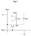
- FIG. 2 is an equivalent circuit diagram of a pixel of the display panel of FIG. 1 .
- FIG. 3 is an equivalent circuit diagram of a touchscreen.
- a display device comprises a display panel DIS, a display drive circuit, a touchscreen TSP, a touchscreen drive circuit, and so on.
- the display panel DIS comprises a liquid crystal layer formed between two substrates.
- On the lower substrate of the display panel DIS formed are a plurality of data lines D1 to Dm (m is a natural number), a plurality of gate lines G1 to Gn (n is a natural number) crossing the data lines D1 to Dm, a plurality of thin film transistors (TFTs) formed at the crossings of the data lines D1 to Dm and the gate lines G1 to Gn, a plurality of pixel electrodes 1 for charging liquid crystal cells with a data voltage, and storage capacitors Cst connected to the pixel electrodes 1 to hold the voltage of the liquid crystal cells.
- TFTs thin film transistors
- a pixel array on the display panel DIS comprises pixels that are formed in pixel regions defined by the data lines D1 to Dm and the gate lines G1 to Gm.
- Each pixel may comprise a liquid crystal cell as shown in FIG. 2 .
- the liquid crystal cell of each pixel is driven by an electric field applied by a voltage difference between a data voltage applied to the pixel electrode 1 and a common voltage Vcom applied to a common electrode 2 to adjust the amount of transmission of incident light.
- the TFTs are turned on by a gate pulse from the gate lines G1 to Gn to supply a data voltage from the data lines D1 to Dm to the pixel electrodes 1 of the liquid crystal cells.
- a black matrix, color filters, etc may be formed on the upper substrate of the display panel DIS.
- the lower substrate of the display panel DIS may be implemented in a COT (color filter on TFT) structure.
- the black matrix and the color filters may be formed on the lower substrate of the display panel DIS.
- the common electrode 2 may be formed on either the upper or lower substrate of the display panel DIS.
- Polarizers are respectively attached to the upper and lower substrates of the display panel DIS, and an alignment film for setting a pre-tilt angle of liquid crystals is formed on an inner surface contacting the liquid crystals.
- a column spacer for maintaining a cell gap of the liquid crystal cells is formed between the upper and lower substrates of the display panel DIS.
- a backlight unit may be disposed under the back of the display panel DIS.
- the backlight unit is an edge-type or direct-type backlight unit which illuminates the display panel DIS.
- the display panel DIS may be implemented in any well-known liquid crystal mode, such as a TN (Twisted Nematic) mode, a VA (Vertical Alignment) mode, an IPS (In-Plane Switching) mode, and an FFS (Fringe Field Switching) mode.
- TN Transmission Nematic
- VA Very Alignment
- IPS In-Plane Switching
- FFS Frringe Field Switching
- the display drive circuit comprises a data drive circuit 12, a scan drive circuit 14, and a display timing controller 20, and writes a video data voltage for an input image to the pixels on the display panel DIS.
- the data drive circuit 12 converts digital video data RGB input from the display timing controller 20 to an analog positive/negative gamma compensation voltage to output a data voltage.
- the data voltage output from the data drive circuit 12 is supplied to the data lines D1 to Dm.
- the scan drive circuit 14 sequentially supplies a gate pulse (or scan pulse) synchronous with the data voltage to select lines on the display panel DIS to which the data voltage is written.
- the pixels on the display panel DIS are charged with the data voltage input from the data drive circuit 12 during a high logic period of a horizontal synchronization signal Hsync, and the data voltage is held during a low logic period of the horizontal synchronization signal Hsync.
- the display timing controller 20 receives timing signals such as a vertical synchronization signal Vsync, a horizontal synchronization signal Hsync, a data enable signal DE, and a main clock MCLK from a host system 40 to synchronize the operation timings of the data drive circuit 12 and scan drive circuit 14 with each other.
- the vertical synchronization signal Vsync is a signal for defining 1 frame period.
- the horizontal synchronization signal Hsync defines 1 horizontal period required to write data to the pixels of one line in the pixel array of the display panel DIS. 1 horizontal period may be calculated by dividing 1 frame period by the number of lines on the display panel DIS.
- One cycle of the horizontal synchronization signal Hsync is set to 1 horizontal period.
- the data enable signal DE defines an effective data input period, and one cycle of the data enable signal DE is set to 1 horizontal period, like the horizontal synchronization signal Hsync. Pulses of the data enable signal DE are generated in synchronization with one line of data, not during a vertical blank VB, but only when effective data is input.
- the vertical blank VB is the time between an Ith frame period (I is a positive integer) and an (I+1)th frame period, during which no data is input.
- the main clock signal MCLK is synchronized with each bit of digital video data.
- the display timing controller 20 generates scan timing control signals for controlling the operation timing of the scan drive circuit 14 and data timing control signals for controlling the operation timing of the data drive circuit 12.
- the scan timing control signals comprise a gate start pulse GSP, a gate shift clock, a gate output enable signal GOE, etc.
- the data timing control signals comprise a source sampling clock SSC, a polarity control signal POL, a source output enable signal SOE, etc.
- the touchscreen TSP comprises Tx lines T1 to TN (N is a positive integer less than n), Rx lines R1 to RM (M is a positive integer less than m) crossing the Tx lines T1 to TN, and (M ⁇ N) touch sensors Cts formed at the crossings of the Tx lines T1 to TN and the Rx lines R1 to RM.
- Each touch sensor Cts comprises mutual capacitance.
- FIG. 4 is an enlarged top plan view of Tx electrodes and Rx electrodes on an in-cell type touchscreen TSP.
- the in-cell type touchscreen TSP will be described in more detail with reference to FIG. 4 .
- Each Tx line comprises transparent Tx channel electrodes T11 to T13 and T21 to T23 that are connected in a transverse direction (x-axis of FIG. 1 ) of the display panel DIS via link patterns L11 to L22.
- the first Tx line T1 comprises the transparent Tx channel electrodes T11 to T13 connected in the transverse direction via the link patterns L11 and L12.
- the second Tx line T2 comprises the transparent Tx channel electrodes T21 to T23 connected in the transverse direction via the link patterns L21 and L22.
- Each of the transparent Tx channel electrodes T11 to T23 is larger in size than the pixels, and overlaps multiple pixels.
- Each of the transparent Tx channel electrodes T11 to T23 overlaps the pixel electrodes 1, with an insulation layer between them.
- Each of the transparent Tx channel electrodes T11 to T23 may be formed of a transparent conductive material such as indium tin oxide (ITO).
- the link patterns L11 to L22 run across the Rx lines R1 and R2, and electrically connect the transparent Tx channel electrodes T11 to T23 neighboring in the transverse direction (or horizontal direction).
- the link patterns L11 to L22 may overlap the Rx lines R1 and R2, with the insulation layer between them.
- the link patterns L11 to L22 may be formed of a metal with high electrical conductivity, for example, aluminum (Al) metal, molybdenum (Mo), chrome (Cr), copper (Cu), or silver (Ag), or a transparent conductive material.
- the Rx lines R1 and R2 are formed in a longitudinal direction (y-axis of FIG. 1 ) of the display panel DIS to cross the Tx lines at right angles.
- the Rx lines R1 and R2 may be formed of a transparent conductive material such as ITO.
- Each of the Rx lines R1 and R2 may overlap multiple pixels (not shown).
- the touchscreen drive circuit 30 applies a Tx drive signal to the Tx lines T1 to TN in every low logic period of the horizontal synchronization signal Hsync and senses the voltage of the touch sensors Cts through the Rx lines R1 to RM.
- a low logic period of the horizontal synchronization signal Hsync comprises a vertical blank VB and a horizontal blank HB.
- the vertical blank VB is the time between neighboring frame periods, during which no data is input.
- the horizontal blank HB is the time between neighboring lines on the pixel array of the display panel DIS, during which no data is written to the pixels.
- the horizontal blank HB equals the time between consecutive gate pulses.
- the touchscreen drive circuit 30 comprises a Tx drive circuit 32, an Rx drive circuit 34, and a touchscreen controller 36 (hereinafter, 'TSP controller').
- the Tx drive circuit 32 selects a Tx channel through which it outputs a Tx drive signal, in response to a Tx setup signal input from the TSP controller 36, and applies the Tx drive signal to the Tx lines T1 to TN connected to the selected Tx channel.
- the Tx lines T1 to TN are charged during a high voltage period of the Tx drive signal to supply electric charges to the touch sensors Cts, and are discharged during a low voltage period of the Tx drive signal.
- the Tx drive signal may be continually supplied N times (N is a positive integer equal to or greater than 2) to the Tx lines T1 to TN through the Rx lines R1 to RM so that a voltage value of the touch sensors Cts is accumulated in an integrator within the Rx drive circuit 34.
- the Rx drive circuit 34 selects an Rx channel through which it receives the voltage of the touch sensors Cts, in response to an Rx setup signal input from the TSP controller 36.
- the Rx drive circuit 34 samples the voltage of the touch sensors Cts received through the Rx lines R1 to RM, and accumulates its value in the integrator. Then, the Rx drive circuit 34 converts the voltage value accumulated in the integrator into digital data using an analog-to-digital converter (hereinafter, 'ADC') connected to an output of the integrator, and outputs touch raw data.
- 'ADC' analog-to-digital converter
- the TSP controller 36 generates a Tx setup signal for setting a Tx channel through which the Tx drive circuit 32 outputs a Tx drive signal, and an Rx setup signal for setting an Rx channel through which the Rx drive circuit 34 receives the voltage of the touch sensors Cts, and synchronizes the sensing operation of the Tx drive circuit 32 and the sensing operation of the Rx drive circuit 34 with each other. Also, the TSP controller 36 generates timing control signals for controlling the operation timing of the sampler and integrator of the Rx drive circuit 34 and the operation timing of the ADC.
- the TSP controller 36 receives a horizontal synchronization signal Hsync from the host system 40, and drives the Tx drive circuit 32 and the Rx drive circuit 34 during touch sensing periods Ts into which the horizontal synchronization signal Hsync is time-divided.
- the Tx drive circuit 32 and the Rx drive circuit 34 sense the voltage of the touch sensors during the touch sensing periods Ts allocated within a low logic period of the horizontal synchronization signal Hsync, under control of the TSP controller 36.
- the TSP controller 36 executes a predetermined touch detection algorithm to compare touch raw data received from the Rx drive circuit 34 with a predetermined threshold value. If the touch raw data is above the threshold value, the touch detection algorithm judges that the touch raw data is data input from touch sensors at touch (or proximity) locations, and calculates the coordinates of each touch (or proximity) location. Then, the TST controller 36 transmits touch report data TR to the host system 40 at a touch report rate higher than a display frame rate.
- the touch report data is created after a touch detection processor 70 detects the presence or absence of a touch on every touch sensor within the touchscreen, and comprises coordinate information of each touch (or proximity) location.
- the host system 40 may be implemented as one of the following: a navigation system, a set-top box, a DVD player, a Blu-ray player, a personal computer (PC), a home theater system, a broadcast receiver, and a phone system.
- FIGS. 5 and 6 are views showing a configuration of a source drive IC SD-IC.
- a source drive IC SD-IC comprises a low-voltage driving block LV_B, a high-voltage driving block HV_B, a first switch LV_SW, a second switch HV_SW, and a switch control part 100.
- the low-voltage driving block LV_B implements digital signal processing by using a power supply voltage VCC.
- the power supply voltage VCC is a voltage of about 3.3 V for operating a logic circuit.
- the low-voltage driving block LV_B comprises a CDR circuit CDR, a shift register S/R, and a latch Latch.
- the shift register S/R samples RGB digital video data bits of an input image using data control signals SSC and SSP received from the timing controller 20, and provides the sampled bits to the latch Latch.
- the latch Latch outputs samples and latches digital video data bits according to clocks sequentially received from the shift register S/R, and outputs the latched data simultaneously, in synchronization with the latches Latch of the other source drive ICs, in response to a source output enable signal SOE.
- the high-voltage driving block HV_B outputs an analog voltage by using a high voltage VDD.
- the high-voltage driving block HV_B comprises a digital-to-analog converter DAC and an output part Amp_CH.
- the digital-to-analog converter DAC converts video data input from the latch Latch into a gamma compensation voltage Gamma to generate an analog video data voltage.
- the output part Amp_CH provides the data lines with an analog data voltage ADATA output from the digital-to-analog converter DAC during a low logic period of the source output enable signal SOE.
- the output part Amp_CH may be implemented as an output buffer for outputting a data voltage using a low voltage GND and a high voltage VDD.
- the second switch HV_SW selectively switches a current path between a high voltage source S_VDD and a high voltage input I_VDD of the high-voltage driving block HV_B.
- a gate electrode of the first switch LV_SW is connected to the switch control part 100, its first electrode is connected to the high voltage source S_VDD, and its second electrode is connected to the high voltage input I_VDD of the high-voltage driving block HV_B.
- the first switch LV_SW selectively switches a current path between a power supply voltage source S_VCC and a power supply voltage input I_VCC of the low-voltage driving block LV_B.
- a gate electrode of the second switch HV_SW is connected to the switch control part 100, its first electrode is connected to the power supply voltage source S_VCC, and its second electrode is connected to the power supply voltage input I_VCC of the low-voltage driving block LV_B.
- the switch control part 100 receives an OFF signal SD_OFF and a touch synchronization signal TSYNC to control the first switch LV_SW and the second switch HV_SW.
- the switch control part 100 controls the first switch LV_SW and the second switch HV_SW under the conditions shown in the following Table 1.
- Table 1 SD_OFF TSYNCN LV_SW HV_SW SD-IC Status 0 0 ON OFF HV_B OFF 0 1 ON ON Normal Operating 1 0 OFF OFF LV_B OFF, HV_B OFF 1 1 OFF OFF LV_B OFF, HV_B OFF
- FIG. 7 is a timing diagram showing an operation of a source drive IC SD-IC based on Table 1. Referring to Table 1 and FIG. 7 , the operation of the source drive IC SD-IC based on the OFF signal SD_OFF and the touch synchronization signal TSYNC will be discussed below.
- the timing controller 20 outputs an OFF signal SD_OFF with a phase opposite to that of an ON signal LCD_ON to the source drive IC SD-IC. That is, the timing controller 20 outputs the OFF signal SD_OFF to the source drive IC SD-IC during active mode. Also, during the active mode, the timing controller 20 outputs, to the source drive IC SD-IC, a touch synchronization signal TSYNC for distinguishing between image display periods Display and touch sensing periods Touch.
- the touch synchronization signal TSYNC is held at low level during the touch sensing periods Touch and at high level during the image display periods Display.
- the switch control part 100 turns off the first switch LV_SW and the second switch HV_SW.
- the first switch LV_SW is turned off, the low-voltage driving block LV_B is disconnected from the power supply voltage source I_VCC.
- the second switch HV_SW is turned off, the high-voltage driving block HV_B is disconnected from the high voltage source S_VDD. That is, neither the low-voltage driving block LV_B nor the high-voltage driving block HV_B operates during sleep mode.
- the exemplary embodiment of the present invention can reduce power consumption since the operation of the source drive IC SD-IC is interrupted during the sleep mode.
- the switch control part 100 turns on the first switch LV_SW and turns off the second switch HV_SW. That is, the high-voltage driving block HV_B is interrupted during the touch sensing periods Touch of the active mode.
- the high-voltage driving block HV_B is not operating, no voltage is output from a channel to the data lines.
- high-impedance mode (Hi-Z mode) effect can be expected, and sensing operations can be performed stably during the touch sensing periods Touch. Consequently, the exemplary embodiment of the present invention allows for an increase in power consumption and stable sensing operations by interrupting the operation of the high-voltage driving block HV_B that consumes large amounts of power during the touch sensing periods Touch.
- the normal operation of the low-voltage driving block LV_B during the touch sensing periods Touch without interruption is related to the recovery time of the source drive IC SD-IC.
- the recovery time of the source drive IC SD-IC is the time required for the source drive IC SD-IC resumes normal operation from interrupted state.
- the CDR circuit CDR generates (number of RGB bits of video data ⁇ 2) internal clocks by inputting an EPI clock into a clock recovery circuit.
- the clock recovery circuit uses a phase locked loop (hereinafter, 'PLL') or a delay locked loop (hereinafter, 'DLL') to output internal clocks and a mask signal and generate a lock signal LOCK.
- 'PLL' phase locked loop
- 'DLL' delay locked loop
- a certain amount of time is needed for clock synchronization, which is defined as Tlock (Power on to DLL Lock Time), as shown in FIG. 8 .
- Tlock Power on to DLL Lock Time
- the low-voltage driving block LV_B comprising the CDR circuit CDR is turned off during the touch sensing periods Touch of the active mode in which the image display periods Display and the touch sensing periods Touch keep alternating, transitions to the image display periods become slow due to the recovery time of the CDR circuit CDR. Accordingly, in the present invention, the low-voltage driving block LV_B, which requires a relatively long period of recovery time, operates normally during the active mode in which images are displayed at intervals.
- the high-voltage driving block HV_B requires a relatively short period of recovery time because only rising and falling times of a buffer's analog voltage are needed as the recovery time in the process of analog voltage output. Accordingly, power consumption can be reduced by not operating the high-voltage driving block HV_B during the touch sensing periods Touch.
- the switch control part 100 turns on the first switch LV_SW and the second switch HV_SW. That is, both the low-voltage driving block LV_B and the high-voltage driving block HV_B operate normally during the image display periods Display, thereby displaying an image.
Landscapes
- Engineering & Computer Science (AREA)
- Theoretical Computer Science (AREA)
- General Engineering & Computer Science (AREA)
- Physics & Mathematics (AREA)
- General Physics & Mathematics (AREA)
- Human Computer Interaction (AREA)
- Computer Hardware Design (AREA)
- Chemical & Material Sciences (AREA)
- Crystallography & Structural Chemistry (AREA)
- Nonlinear Science (AREA)
- Computing Systems (AREA)
- Mathematical Physics (AREA)
- Optics & Photonics (AREA)
- Control Of Indicators Other Than Cathode Ray Tubes (AREA)
- Liquid Crystal Display Device Control (AREA)
Abstract
Description
- This application claims the benefit of
Korean Patent Application No. 10-2014-0195728 filed on December 31, 2014 - This document relates to a touch sensor integrated type display device.
- User interfaces (UI) enable humans (users) to interact with various types of electric or electronic devices so that they can easily control the devices as they want. Typical examples of the user interfaces include keypads, keyboards, mice, on-screen displays (OSD), and remote controllers with an infrared communication capability or radio frequency (RF) communication capability. The user interface technology is continuing make progress toward increasing user sensitivity and ease of operation. Recently, user interfaces have been evolving into touch UI, voice recognition UI, 3D UI, etc. The adoption of touch UIs for portable information devices is becoming essential, and moreover, the touch UIs are expanding its range of application to home appliances. Capacitive touchscreens can be used in a variety of applications since they have higher durability and better contrast than conventional resistive touchscreens and allow for multi-touch sensing and proximity-touch sensing.
- In recent years, there has been a growing demand for in-cell type (hereinafter, in-cell) touch screen integrated-type display devices incorporating elements constituting a touchscreen to make portable terminals such as smartphones, tablet PCs, etc slimmer. In the in-cell touchscreen integrated type display devices, common electrodes for display are segmented into those for a plurality of touch driving periods and those for a plurality of touch sensing periods so that mutual capacitance occurs between the touch driving periods and the touch sensing periods. Therefore, the in-cell touchscreen integrated type display devices can detect a touch by measuring a change in mutual capacitance made by the touch.
- In the touch sensing periods, the electric potential of other electrodes or signal lines than sensor electrodes must not be changed. Accordingly, during the touch sensing periods, data lines remain at a specific voltage value or their current path to a channel is blocked. A data driver keeps operating when the current path between the channel and the data lines is blocked, as well as when a specific voltage is applied to the data lines. That is, electric power is constantly consumed while the data driver is not actually operating, which results in unnecessary waste of electricity.
- A touch sensor integrated type display device according to the present invention may comprise: a display panel; a low-voltage driving block, a high-voltage driving block, a first switch, a second switch, and a switch control part. The low-voltage driving block receives image data for display on the display panel and implements digital signal processing on the image data. The high-voltage driving block generates a data voltage corresponding to the image data and outputs the data voltage to data lines. The first switch connects a power supply voltage source and the low-voltage driving block, and the second switch connects a high voltage source and the high-voltage driving block. The switch control part controls operations of the first and second switches.
- The switch control part may control the first and second switches by using an off signal for distinguishing between active mode and sleep mode; and a touch synchronization signal for distinguishing between image display periods and touch sensing periods during the active mode.
- Further, the switch control part may turn off both the first and second switches during the sleep mode.
- In addition, the switch control part may turn on the first switch and turn off the second switch during the touch sensing periods.
- Finally, the low-voltage driving block may comprise a CDR circuit that performs clock synchronization and generates internal clocks.
- The accompanying drawings, which are included to provide a further understanding of the invention and are incorporated in and constitute a part of this specification, illustrate embodiments of the invention and together with the description serve to explain the principles of the invention. In the drawings:
-
FIG. 1 is a view showing a touch sensor integrated type display device according to an exemplary embodiment of the present invention; -
FIG. 2 is an equivalent circuit diagram of a liquid crystal cell; -
FIG. 3 is an equivalent circuit diagram of a touchscreen; -
FIG. 4 is a view showing a driving electrode array structure of an in-cell type touchscreen; -
FIGS. 5 and6 are views showing a source drive IC according to an exemplary embodiment of the present invention; -
FIG. 7 is a view showing a control method for a source drive IC according to an exemplary embodiment of the present invention; and -
FIG. 8 is a view showing an example of a clock recovery sequence. - Hereinafter, exemplary embodiments of the present invention will be described in detail with reference to the attached drawings.
-
FIG. 1 is a view showing a touch sensor integrated type display device according to an exemplary embodiment of the present invention.FIG. 2 is an equivalent circuit diagram of a pixel of the display panel ofFIG. 1 .FIG. 3 is an equivalent circuit diagram of a touchscreen. - A display device according to an exemplary embodiment of the present invention comprises a display panel DIS, a display drive circuit, a touchscreen TSP, a touchscreen drive circuit, and so on.
- Referring to
FIGS. 1 and2 , the display panel DIS comprises a liquid crystal layer formed between two substrates. On the lower substrate of the display panel DIS formed are a plurality of data lines D1 to Dm (m is a natural number), a plurality of gate lines G1 to Gn (n is a natural number) crossing the data lines D1 to Dm, a plurality of thin film transistors (TFTs) formed at the crossings of the data lines D1 to Dm and the gate lines G1 to Gn, a plurality ofpixel electrodes 1 for charging liquid crystal cells with a data voltage, and storage capacitors Cst connected to thepixel electrodes 1 to hold the voltage of the liquid crystal cells. - A pixel array on the display panel DIS comprises pixels that are formed in pixel regions defined by the data lines D1 to Dm and the gate lines G1 to Gm. Each pixel may comprise a liquid crystal cell as shown in
FIG. 2 . The liquid crystal cell of each pixel is driven by an electric field applied by a voltage difference between a data voltage applied to thepixel electrode 1 and a common voltage Vcom applied to acommon electrode 2 to adjust the amount of transmission of incident light. The TFTs are turned on by a gate pulse from the gate lines G1 to Gn to supply a data voltage from the data lines D1 to Dm to thepixel electrodes 1 of the liquid crystal cells. - On the upper substrate of the display panel DIS, a black matrix, color filters, etc may be formed. The lower substrate of the display panel DIS may be implemented in a COT (color filter on TFT) structure. In this case, the black matrix and the color filters may be formed on the lower substrate of the display panel DIS. The
common electrode 2 may be formed on either the upper or lower substrate of the display panel DIS. - Polarizers are respectively attached to the upper and lower substrates of the display panel DIS, and an alignment film for setting a pre-tilt angle of liquid crystals is formed on an inner surface contacting the liquid crystals. A column spacer for maintaining a cell gap of the liquid crystal cells is formed between the upper and lower substrates of the display panel DIS.
- A backlight unit may be disposed under the back of the display panel DIS. The backlight unit is an edge-type or direct-type backlight unit which illuminates the display panel DIS. The display panel DIS may be implemented in any well-known liquid crystal mode, such as a TN (Twisted Nematic) mode, a VA (Vertical Alignment) mode, an IPS (In-Plane Switching) mode, and an FFS (Fringe Field Switching) mode.
- The display drive circuit comprises a
data drive circuit 12, ascan drive circuit 14, and adisplay timing controller 20, and writes a video data voltage for an input image to the pixels on the display panel DIS. Thedata drive circuit 12 converts digital video data RGB input from thedisplay timing controller 20 to an analog positive/negative gamma compensation voltage to output a data voltage. The data voltage output from thedata drive circuit 12 is supplied to the data lines D1 to Dm. Thescan drive circuit 14 sequentially supplies a gate pulse (or scan pulse) synchronous with the data voltage to select lines on the display panel DIS to which the data voltage is written. In response to the scan pulse, the pixels on the display panel DIS are charged with the data voltage input from thedata drive circuit 12 during a high logic period of a horizontal synchronization signal Hsync, and the data voltage is held during a low logic period of the horizontal synchronization signal Hsync. - The
display timing controller 20 receives timing signals such as a vertical synchronization signal Vsync, a horizontal synchronization signal Hsync, a data enable signal DE, and a main clock MCLK from ahost system 40 to synchronize the operation timings of thedata drive circuit 12 and scandrive circuit 14 with each other. The vertical synchronization signal Vsync is a signal for defining 1 frame period. The horizontal synchronization signal Hsync defines 1 horizontal period required to write data to the pixels of one line in the pixel array of the display panel DIS. 1 horizontal period may be calculated by dividing 1 frame period by the number of lines on the display panel DIS. One cycle of the horizontal synchronization signal Hsync is set to 1 horizontal period. The data enable signal DE defines an effective data input period, and one cycle of the data enable signal DE is set to 1 horizontal period, like the horizontal synchronization signal Hsync. Pulses of the data enable signal DE are generated in synchronization with one line of data, not during a vertical blank VB, but only when effective data is input. The vertical blank VB is the time between an Ith frame period (I is a positive integer) and an (I+1)th frame period, during which no data is input. The main clock signal MCLK is synchronized with each bit of digital video data. - The
display timing controller 20 generates scan timing control signals for controlling the operation timing of thescan drive circuit 14 and data timing control signals for controlling the operation timing of the data drivecircuit 12. The scan timing control signals comprise a gate start pulse GSP, a gate shift clock, a gate output enable signal GOE, etc. The data timing control signals comprise a source sampling clock SSC, a polarity control signal POL, a source output enable signal SOE, etc. - As shown in
FIG. 3 , the touchscreen TSP comprises Tx lines T1 to TN (N is a positive integer less than n), Rx lines R1 to RM (M is a positive integer less than m) crossing the Tx lines T1 to TN, and (M×N) touch sensors Cts formed at the crossings of the Tx lines T1 to TN and the Rx lines R1 to RM. Each touch sensor Cts comprises mutual capacitance. -
FIG. 4 is an enlarged top plan view of Tx electrodes and Rx electrodes on an in-cell type touchscreen TSP. The in-cell type touchscreen TSP will be described in more detail with reference toFIG. 4 . - Each Tx line comprises transparent Tx channel electrodes T11 to T13 and T21 to T23 that are connected in a transverse direction (x-axis of
FIG. 1 ) of the display panel DIS via link patterns L11 to L22. The first Tx line T1 comprises the transparent Tx channel electrodes T11 to T13 connected in the transverse direction via the link patterns L11 and L12. The second Tx line T2 comprises the transparent Tx channel electrodes T21 to T23 connected in the transverse direction via the link patterns L21 and L22. Each of the transparent Tx channel electrodes T11 to T23 is larger in size than the pixels, and overlaps multiple pixels. Each of the transparent Tx channel electrodes T11 to T23 overlaps thepixel electrodes 1, with an insulation layer between them. Each of the transparent Tx channel electrodes T11 to T23 may be formed of a transparent conductive material such as indium tin oxide (ITO). The link patterns L11 to L22 run across the Rx lines R1 and R2, and electrically connect the transparent Tx channel electrodes T11 to T23 neighboring in the transverse direction (or horizontal direction). The link patterns L11 to L22 may overlap the Rx lines R1 and R2, with the insulation layer between them. The link patterns L11 to L22 may be formed of a metal with high electrical conductivity, for example, aluminum (Al) metal, molybdenum (Mo), chrome (Cr), copper (Cu), or silver (Ag), or a transparent conductive material. - The Rx lines R1 and R2 are formed in a longitudinal direction (y-axis of
FIG. 1 ) of the display panel DIS to cross the Tx lines at right angles. The Rx lines R1 and R2 may be formed of a transparent conductive material such as ITO. Each of the Rx lines R1 and R2 may overlap multiple pixels (not shown). - The
touchscreen drive circuit 30 applies a Tx drive signal to the Tx lines T1 to TN in every low logic period of the horizontal synchronization signal Hsync and senses the voltage of the touch sensors Cts through the Rx lines R1 to RM. As shown inFIG. 7 , a low logic period of the horizontal synchronization signal Hsync comprises a vertical blank VB and a horizontal blank HB. As stated above, the vertical blank VB is the time between neighboring frame periods, during which no data is input. The horizontal blank HB is the time between neighboring lines on the pixel array of the display panel DIS, during which no data is written to the pixels. The horizontal blank HB equals the time between consecutive gate pulses. - The
touchscreen drive circuit 30 comprises a Tx drive circuit 32, anRx drive circuit 34, and a touchscreen controller 36 (hereinafter, 'TSP controller'). - The Tx drive circuit 32 selects a Tx channel through which it outputs a Tx drive signal, in response to a Tx setup signal input from the
TSP controller 36, and applies the Tx drive signal to the Tx lines T1 to TN connected to the selected Tx channel. The Tx lines T1 to TN are charged during a high voltage period of the Tx drive signal to supply electric charges to the touch sensors Cts, and are discharged during a low voltage period of the Tx drive signal. The Tx drive signal may be continually supplied N times (N is a positive integer equal to or greater than 2) to the Tx lines T1 to TN through the Rx lines R1 to RM so that a voltage value of the touch sensors Cts is accumulated in an integrator within theRx drive circuit 34. - The
Rx drive circuit 34 selects an Rx channel through which it receives the voltage of the touch sensors Cts, in response to an Rx setup signal input from theTSP controller 36. TheRx drive circuit 34 samples the voltage of the touch sensors Cts received through the Rx lines R1 to RM, and accumulates its value in the integrator. Then, theRx drive circuit 34 converts the voltage value accumulated in the integrator into digital data using an analog-to-digital converter (hereinafter, 'ADC') connected to an output of the integrator, and outputs touch raw data. - The
TSP controller 36 generates a Tx setup signal for setting a Tx channel through which the Tx drive circuit 32 outputs a Tx drive signal, and an Rx setup signal for setting an Rx channel through which theRx drive circuit 34 receives the voltage of the touch sensors Cts, and synchronizes the sensing operation of the Tx drive circuit 32 and the sensing operation of theRx drive circuit 34 with each other. Also, theTSP controller 36 generates timing control signals for controlling the operation timing of the sampler and integrator of theRx drive circuit 34 and the operation timing of the ADC. - The
TSP controller 36 receives a horizontal synchronization signal Hsync from thehost system 40, and drives the Tx drive circuit 32 and theRx drive circuit 34 during touch sensing periods Ts into which the horizontal synchronization signal Hsync is time-divided. The Tx drive circuit 32 and theRx drive circuit 34 sense the voltage of the touch sensors during the touch sensing periods Ts allocated within a low logic period of the horizontal synchronization signal Hsync, under control of theTSP controller 36. - The
TSP controller 36 executes a predetermined touch detection algorithm to compare touch raw data received from theRx drive circuit 34 with a predetermined threshold value. If the touch raw data is above the threshold value, the touch detection algorithm judges that the touch raw data is data input from touch sensors at touch (or proximity) locations, and calculates the coordinates of each touch (or proximity) location. Then, theTST controller 36 transmits touch report data TR to thehost system 40 at a touch report rate higher than a display frame rate. The touch report data is created after a touch detection processor 70 detects the presence or absence of a touch on every touch sensor within the touchscreen, and comprises coordinate information of each touch (or proximity) location. - The
host system 40 may be implemented as one of the following: a navigation system, a set-top box, a DVD player, a Blu-ray player, a personal computer (PC), a home theater system, a broadcast receiver, and a phone system. -
FIGS. 5 and6 are views showing a configuration of a source drive IC SD-IC. - Referring to
FIGS. 5 and6 , a source drive IC SD-IC according to the present invention comprises a low-voltage driving block LV_B, a high-voltage driving block HV_B, a first switch LV_SW, a second switch HV_SW, and aswitch control part 100. - The low-voltage driving block LV_B implements digital signal processing by using a power supply voltage VCC. The power supply voltage VCC is a voltage of about 3.3 V for operating a logic circuit. The low-voltage driving block LV_B comprises a CDR circuit CDR, a shift register S/R, and a latch Latch. The shift register S/R samples RGB digital video data bits of an input image using data control signals SSC and SSP received from the
timing controller 20, and provides the sampled bits to the latch Latch. The latch Latch outputs samples and latches digital video data bits according to clocks sequentially received from the shift register S/R, and outputs the latched data simultaneously, in synchronization with the latches Latch of the other source drive ICs, in response to a source output enable signal SOE. - The high-voltage driving block HV_B outputs an analog voltage by using a high voltage VDD. The high-voltage driving block HV_B comprises a digital-to-analog converter DAC and an output part Amp_CH. The digital-to-analog converter DAC converts video data input from the latch Latch into a gamma compensation voltage Gamma to generate an analog video data voltage. The output part Amp_CH provides the data lines with an analog data voltage ADATA output from the digital-to-analog converter DAC during a low logic period of the source output enable signal SOE. The output part Amp_CH may be implemented as an output buffer for outputting a data voltage using a low voltage GND and a high voltage VDD.
- The second switch HV_SW selectively switches a current path between a high voltage source S_VDD and a high voltage input I_VDD of the high-voltage driving block HV_B. A gate electrode of the first switch LV_SW is connected to the
switch control part 100, its first electrode is connected to the high voltage source S_VDD, and its second electrode is connected to the high voltage input I_VDD of the high-voltage driving block HV_B. - The first switch LV_SW selectively switches a current path between a power supply voltage source S_VCC and a power supply voltage input I_VCC of the low-voltage driving block LV_B. A gate electrode of the second switch HV_SW is connected to the
switch control part 100, its first electrode is connected to the power supply voltage source S_VCC, and its second electrode is connected to the power supply voltage input I_VCC of the low-voltage driving block LV_B. - The
switch control part 100 receives an OFF signal SD_OFF and a touch synchronization signal TSYNC to control the first switch LV_SW and the second switch HV_SW. - The
switch control part 100 controls the first switch LV_SW and the second switch HV_SW under the conditions shown in the following Table 1.[Table 1] SD_OFF TSYNCN LV_SW HV_SW SD-IC Status 0 0 ON OFF HV_B OFF 0 1 ON ON Normal Operating 1 0 OFF OFF LV_B OFF, HV_B OFF 1 1 OFF OFF LV_B OFF, HV_B OFF -
FIG. 7 is a timing diagram showing an operation of a source drive IC SD-IC based on Table 1. Referring to Table 1 andFIG. 7 , the operation of the source drive IC SD-IC based on the OFF signal SD_OFF and the touch synchronization signal TSYNC will be discussed below. - The
timing controller 20 outputs an OFF signal SD_OFF with a phase opposite to that of an ON signal LCD_ON to the source drive IC SD-IC. That is, thetiming controller 20 outputs the OFF signal SD_OFF to the source drive IC SD-IC during active mode. Also, during the active mode, thetiming controller 20 outputs, to the source drive IC SD-IC, a touch synchronization signal TSYNC for distinguishing between image display periods Display and touch sensing periods Touch. The touch synchronization signal TSYNC is held at low level during the touch sensing periods Touch and at high level during the image display periods Display. - If the OFF signal SD_OFF is at high level, the
switch control part 100 turns off the first switch LV_SW and the second switch HV_SW. When the first switch LV_SW is turned off, the low-voltage driving block LV_B is disconnected from the power supply voltage source I_VCC. When the second switch HV_SW is turned off, the high-voltage driving block HV_B is disconnected from the high voltage source S_VDD. That is, neither the low-voltage driving block LV_B nor the high-voltage driving block HV_B operates during sleep mode. As such, the exemplary embodiment of the present invention can reduce power consumption since the operation of the source drive IC SD-IC is interrupted during the sleep mode. - While the OFF signal SD_OFF is at low level, if the touch synchronization signal TSYNC is low level, the
switch control part 100 turns on the first switch LV_SW and turns off the second switch HV_SW. That is, the high-voltage driving block HV_B is interrupted during the touch sensing periods Touch of the active mode. When the high-voltage driving block HV_B is not operating, no voltage is output from a channel to the data lines. By interrupting the operation of the high-voltage driving block HV_B, high-impedance mode (Hi-Z mode) effect can be expected, and sensing operations can be performed stably during the touch sensing periods Touch. Consequently, the exemplary embodiment of the present invention allows for an increase in power consumption and stable sensing operations by interrupting the operation of the high-voltage driving block HV_B that consumes large amounts of power during the touch sensing periods Touch. - The normal operation of the low-voltage driving block LV_B during the touch sensing periods Touch without interruption is related to the recovery time of the source drive IC SD-IC.
- The recovery time of the source drive IC SD-IC is the time required for the source drive IC SD-IC resumes normal operation from interrupted state.
- The recovery time will be explained below.
- The CDR circuit CDR generates (number of RGB bits of video data ×2) internal clocks by inputting an EPI clock into a clock recovery circuit. The clock recovery circuit uses a phase locked loop (hereinafter, 'PLL') or a delay locked loop (hereinafter, 'DLL') to output internal clocks and a mask signal and generate a lock signal LOCK. In the operation of the clock recovery circuit of the CDR circuit CDR, a certain amount of time is needed for clock synchronization, which is defined as Tlock (Power on to DLL Lock Time), as shown in
FIG. 8 . During the 'Tlock' period, the CDR circuit CDR of the source drive IC SD-IC checks whether it is synchronized with an input clock, transmits feedback signal to thetiming controller 20, and then receives normal data RGB data from thetiming controller 20. - As stated above, a signal feedback time is needed for the CDR circuit CDR to perform clock synchronization and check whether clock synchronization is done. Thus, it takes a relatively long time before normal operation is resumed. When the low-voltage driving block LV_B comprising the CDR circuit CDR is turned off during the touch sensing periods Touch of the active mode in which the image display periods Display and the touch sensing periods Touch keep alternating, transitions to the image display periods become slow due to the recovery time of the CDR circuit CDR. Accordingly, in the present invention, the low-voltage driving block LV_B, which requires a relatively long period of recovery time, operates normally during the active mode in which images are displayed at intervals.
- In contrast, the high-voltage driving block HV_B requires a relatively short period of recovery time because only rising and falling times of a buffer's analog voltage are needed as the recovery time in the process of analog voltage output. Accordingly, power consumption can be reduced by not operating the high-voltage driving block HV_B during the touch sensing periods Touch.
- While the OFF signal SD_OFF is at low level, if the touch synchronization signal TSYNC is high level, the
switch control part 100 turns on the first switch LV_SW and the second switch HV_SW. That is, both the low-voltage driving block LV_B and the high-voltage driving block HV_B operate normally during the image display periods Display, thereby displaying an image. - Although embodiments have been described with reference to a number of illustrative embodiments thereof, it should be understood that numerous other modifications and embodiments can be devised by those skilled in the art that will fall within the spirit and scope of the principles of this disclosure. More particularly, various variations and modifications are possible in the component parts and/or arrangements of the subject combination arrangement within the scope of the disclosure, the drawings and the appended claims. In addition to variations and modifications in the component parts and/or arrangements, alternative uses will also be apparent to those skilled in the art.
Claims (5)
- A touch sensor integrated type display device comprising:a display panel with data lines (D1 to Dm) arranged thereon;a low-voltage driving block (LV_B) that receives image data for display on the display panel and implements digital signal processing on the image data;a high-voltage driving block (HV_B) that generates a data voltage corresponding to the image data and outputs the data voltage to the data lines (D1 to Dm) ;a first switch (LV_SW) that connects a power supply voltage source (S_VCC) and the low-voltage driving block (LV_B);a second switch (HV_SW) that connects a high voltage source (S_VDD) and the high-voltage driving block (HV_B); anda switch control part (100) that controls operations of the first (LV_SW) and second switches (HV_SW).
- The touch sensor integrated type display device of claim 1, wherein the switch control part (100) controls the first (LV_SW) and second (HV_SW) switches by using:an off signal for distinguishing between active mode and sleep mode; anda touch synchronization signal for distinguishing between image display periods and touch sensing periods during the active mode.
- The touch sensor integrated type display device of claim 2, wherein the switch control part (100) turns off both the first (LV_SW) and second (HV_SW) switches during the sleep mode.
- The touch sensor integrated type display device of claim 2 or 3, wherein the switch control part (100) turns on the first switch (LV_SW) and turns off the second switch (HV_SW) during the touch sensing periods.
- The touch sensor integrated type display device of any one of the claims 1 to 4, wherein the low-voltage driving block (LV_B) comprises a CDR circuit that performs clock synchronization and generates internal clocks.
Priority Applications (1)
| Application Number | Priority Date | Filing Date | Title |
|---|---|---|---|
| PL15198202T PL3040824T3 (en) | 2014-12-31 | 2015-12-07 | Touch sensor integrated type display device |
Applications Claiming Priority (1)
| Application Number | Priority Date | Filing Date | Title |
|---|---|---|---|
| KR1020140195728A KR102285910B1 (en) | 2014-12-31 | 2014-12-31 | Touch sensor intergrated display devive |
Publications (2)
| Publication Number | Publication Date |
|---|---|
| EP3040824A1 true EP3040824A1 (en) | 2016-07-06 |
| EP3040824B1 EP3040824B1 (en) | 2017-08-16 |
Family
ID=54834690
Family Applications (1)
| Application Number | Title | Priority Date | Filing Date |
|---|---|---|---|
| EP15198202.2A Active EP3040824B1 (en) | 2014-12-31 | 2015-12-07 | Touch sensor integrated type display device |
Country Status (6)
| Country | Link |
|---|---|
| US (1) | US9946382B2 (en) |
| EP (1) | EP3040824B1 (en) |
| KR (1) | KR102285910B1 (en) |
| CN (1) | CN105739738B (en) |
| ES (1) | ES2647123T3 (en) |
| PL (1) | PL3040824T3 (en) |
Families Citing this family (9)
| Publication number | Priority date | Publication date | Assignee | Title |
|---|---|---|---|---|
| US9940865B2 (en) * | 2015-06-18 | 2018-04-10 | Panasonic Liquid Crystal Display Co., Ltd. | Liquid crystal display device |
| CN105243991B (en) * | 2015-10-27 | 2018-01-26 | 深圳市华星光电技术有限公司 | AMOLED drive devices |
| CN107515689B (en) * | 2017-06-29 | 2020-11-03 | 成都天马微电子有限公司 | Display panel, display device, and driving method of display panel |
| KR102385631B1 (en) * | 2017-10-24 | 2022-04-11 | 엘지디스플레이 주식회사 | Touch display device |
| US10832632B2 (en) | 2018-03-14 | 2020-11-10 | Samsung Display Co., Ltd. | Low power architecture for mobile displays |
| US10885871B2 (en) * | 2018-03-14 | 2021-01-05 | Samsung Display Co., Ltd. | Scalable driving architecture for large size displays |
| CN110346955B (en) * | 2019-06-24 | 2021-01-01 | 武汉华星光电技术有限公司 | Touch array substrate and touch screen |
| US11625939B2 (en) * | 2019-08-01 | 2023-04-11 | Novatek Microelectronics Corp. | Electronic circuit having display driving function, touch sensing function and fingerprint sensing function |
| CN112581894B (en) * | 2019-09-30 | 2022-08-26 | 京东方科技集团股份有限公司 | Display device and power supply method thereof |
Citations (4)
| Publication number | Priority date | Publication date | Assignee | Title |
|---|---|---|---|---|
| EP2056282A2 (en) * | 2007-10-29 | 2009-05-06 | Samsung Mobile Display Co., Ltd. | Organic light emitting display and power supply method thereof |
| US20100110040A1 (en) * | 2008-10-30 | 2010-05-06 | Samsung Electronics Co., Ltd. | Touch controller having increased sensing sensitivity, and display driving circuit and display device and system having the touch controller |
| EP2503435A2 (en) * | 2011-03-25 | 2012-09-26 | LG Display Co., Ltd. | Display with integrated touch sensor and driving method thereof |
| US20140204041A1 (en) * | 2013-01-24 | 2014-07-24 | Renesas Sp Drivers Inc. | Semiconductor device |
Family Cites Families (5)
| Publication number | Priority date | Publication date | Assignee | Title |
|---|---|---|---|---|
| KR101716781B1 (en) * | 2010-08-20 | 2017-03-16 | 삼성디스플레이 주식회사 | Display apparatus and method of providing power thereof |
| US9201540B2 (en) * | 2011-09-07 | 2015-12-01 | Apple Inc. | Charge recycling system and method |
| KR101992904B1 (en) * | 2012-12-21 | 2019-06-26 | 엘지디스플레이 주식회사 | Organic light emitting diode display device and driving method the same |
| KR101528459B1 (en) * | 2013-03-26 | 2015-06-12 | 주식회사 실리콘웍스 | Source driver for display apparatus |
| CN103413523B (en) * | 2013-07-31 | 2015-05-27 | 京东方科技集团股份有限公司 | Pixel circuit, organic electroluminescence display panel and display device |
-
2014
- 2014-12-31 KR KR1020140195728A patent/KR102285910B1/en active IP Right Grant
-
2015
- 2015-11-10 CN CN201510762759.8A patent/CN105739738B/en active Active
- 2015-12-07 EP EP15198202.2A patent/EP3040824B1/en active Active
- 2015-12-07 PL PL15198202T patent/PL3040824T3/en unknown
- 2015-12-07 ES ES15198202.2T patent/ES2647123T3/en active Active
- 2015-12-21 US US14/977,519 patent/US9946382B2/en active Active
Patent Citations (4)
| Publication number | Priority date | Publication date | Assignee | Title |
|---|---|---|---|---|
| EP2056282A2 (en) * | 2007-10-29 | 2009-05-06 | Samsung Mobile Display Co., Ltd. | Organic light emitting display and power supply method thereof |
| US20100110040A1 (en) * | 2008-10-30 | 2010-05-06 | Samsung Electronics Co., Ltd. | Touch controller having increased sensing sensitivity, and display driving circuit and display device and system having the touch controller |
| EP2503435A2 (en) * | 2011-03-25 | 2012-09-26 | LG Display Co., Ltd. | Display with integrated touch sensor and driving method thereof |
| US20140204041A1 (en) * | 2013-01-24 | 2014-07-24 | Renesas Sp Drivers Inc. | Semiconductor device |
Also Published As
| Publication number | Publication date |
|---|---|
| KR20160083559A (en) | 2016-07-12 |
| US20160188062A1 (en) | 2016-06-30 |
| CN105739738A (en) | 2016-07-06 |
| KR102285910B1 (en) | 2021-08-06 |
| PL3040824T3 (en) | 2018-01-31 |
| CN105739738B (en) | 2018-12-14 |
| US9946382B2 (en) | 2018-04-17 |
| EP3040824B1 (en) | 2017-08-16 |
| ES2647123T3 (en) | 2017-12-19 |
Similar Documents
| Publication | Publication Date | Title |
|---|---|---|
| EP3040824B1 (en) | Touch sensor integrated type display device | |
| US10175803B2 (en) | Touch sensing device and method for driving the same | |
| US10282018B2 (en) | Display device | |
| US9024913B1 (en) | Touch sensing device and driving method thereof | |
| KR102305323B1 (en) | Touch sensing device | |
| US9058072B2 (en) | Touch sensing apparatus and driving method thereof | |
| KR101615813B1 (en) | Touch sensing apparatus for time division driving type | |
| US9245490B1 (en) | Display device and data driving circuit thereof | |
| US9513742B2 (en) | Touch sensing system | |
| US9910333B2 (en) | Display device | |
| US9430088B1 (en) | Touch sensor driving device and display device comprising the same | |
| KR101731174B1 (en) | Touch sensor integrated type display device | |
| KR102285909B1 (en) | Touch sensor intergrated type display device | |
| KR101798662B1 (en) | Apparatus and method for driving touch screen |
Legal Events
| Date | Code | Title | Description |
|---|---|---|---|
| PUAI | Public reference made under article 153(3) epc to a published international application that has entered the european phase |
Free format text: ORIGINAL CODE: 0009012 |
|
| 17P | Request for examination filed |
Effective date: 20151207 |
|
| AK | Designated contracting states |
Kind code of ref document: A1 Designated state(s): AL AT BE BG CH CY CZ DE DK EE ES FI FR GB GR HR HU IE IS IT LI LT LU LV MC MK MT NL NO PL PT RO RS SE SI SK SM TR |
|
| AX | Request for extension of the european patent |
Extension state: BA ME |
|
| REG | Reference to a national code |
Ref country code: DE Ref legal event code: R079 Ref document number: 602015004157 Country of ref document: DE Free format text: PREVIOUS MAIN CLASS: G06F0003041000 Ipc: G06F0001320000 |
|
| RBV | Designated contracting states (corrected) |
Designated state(s): AL AT BE BG CH CY CZ DE DK EE ES FI FR GB GR HR HU IE IS IT LI LT LU LV MC MK MT NL NO PL PT RO RS SE SI SK SM TR |
|
| GRAP | Despatch of communication of intention to grant a patent |
Free format text: ORIGINAL CODE: EPIDOSNIGR1 |
|
| RIC1 | Information provided on ipc code assigned before grant |
Ipc: G09G 3/36 20060101ALI20170221BHEP Ipc: G02F 1/1333 20060101ALI20170221BHEP Ipc: G06F 1/32 20060101AFI20170221BHEP Ipc: G06F 3/044 20060101ALI20170221BHEP Ipc: G06F 3/041 20060101ALI20170221BHEP |
|
| INTG | Intention to grant announced |
Effective date: 20170307 |
|
| GRAS | Grant fee paid |
Free format text: ORIGINAL CODE: EPIDOSNIGR3 |
|
| GRAA | (expected) grant |
Free format text: ORIGINAL CODE: 0009210 |
|
| AK | Designated contracting states |
Kind code of ref document: B1 Designated state(s): AL AT BE BG CH CY CZ DE DK EE ES FI FR GB GR HR HU IE IS IT LI LT LU LV MC MK MT NL NO PL PT RO RS SE SI SK SM TR |
|
| REG | Reference to a national code |
Ref country code: GB Ref legal event code: FG4D |
|
| REG | Reference to a national code |
Ref country code: CH Ref legal event code: EP |
|
| REG | Reference to a national code |
Ref country code: IE Ref legal event code: FG4D |
|
| REG | Reference to a national code |
Ref country code: AT Ref legal event code: REF Ref document number: 919669 Country of ref document: AT Kind code of ref document: T Effective date: 20170915 |
|
| REG | Reference to a national code |
Ref country code: DE Ref legal event code: R096 Ref document number: 602015004157 Country of ref document: DE |
|
| REG | Reference to a national code |
Ref country code: NL Ref legal event code: FP |
|
| REG | Reference to a national code |
Ref country code: ES Ref legal event code: FG2A Ref document number: 2647123 Country of ref document: ES Kind code of ref document: T3 Effective date: 20171219 Ref country code: FR Ref legal event code: PLFP Year of fee payment: 3 |
|
| REG | Reference to a national code |
Ref country code: LT Ref legal event code: MG4D |
|
| REG | Reference to a national code |
Ref country code: AT Ref legal event code: MK05 Ref document number: 919669 Country of ref document: AT Kind code of ref document: T Effective date: 20170816 |
|
| PG25 | Lapsed in a contracting state [announced via postgrant information from national office to epo] |
Ref country code: LT Free format text: LAPSE BECAUSE OF FAILURE TO SUBMIT A TRANSLATION OF THE DESCRIPTION OR TO PAY THE FEE WITHIN THE PRESCRIBED TIME-LIMIT Effective date: 20170816 Ref country code: AT Free format text: LAPSE BECAUSE OF FAILURE TO SUBMIT A TRANSLATION OF THE DESCRIPTION OR TO PAY THE FEE WITHIN THE PRESCRIBED TIME-LIMIT Effective date: 20170816 Ref country code: NO Free format text: LAPSE BECAUSE OF FAILURE TO SUBMIT A TRANSLATION OF THE DESCRIPTION OR TO PAY THE FEE WITHIN THE PRESCRIBED TIME-LIMIT Effective date: 20171116 Ref country code: FI Free format text: LAPSE BECAUSE OF FAILURE TO SUBMIT A TRANSLATION OF THE DESCRIPTION OR TO PAY THE FEE WITHIN THE PRESCRIBED TIME-LIMIT Effective date: 20170816 Ref country code: SE Free format text: LAPSE BECAUSE OF FAILURE TO SUBMIT A TRANSLATION OF THE DESCRIPTION OR TO PAY THE FEE WITHIN THE PRESCRIBED TIME-LIMIT Effective date: 20170816 |
|
| PG25 | Lapsed in a contracting state [announced via postgrant information from national office to epo] |
Ref country code: RS Free format text: LAPSE BECAUSE OF FAILURE TO SUBMIT A TRANSLATION OF THE DESCRIPTION OR TO PAY THE FEE WITHIN THE PRESCRIBED TIME-LIMIT Effective date: 20170816 Ref country code: GR Free format text: LAPSE BECAUSE OF FAILURE TO SUBMIT A TRANSLATION OF THE DESCRIPTION OR TO PAY THE FEE WITHIN THE PRESCRIBED TIME-LIMIT Effective date: 20171117 Ref country code: IS Free format text: LAPSE BECAUSE OF FAILURE TO SUBMIT A TRANSLATION OF THE DESCRIPTION OR TO PAY THE FEE WITHIN THE PRESCRIBED TIME-LIMIT Effective date: 20171216 Ref country code: LV Free format text: LAPSE BECAUSE OF FAILURE TO SUBMIT A TRANSLATION OF THE DESCRIPTION OR TO PAY THE FEE WITHIN THE PRESCRIBED TIME-LIMIT Effective date: 20170816 Ref country code: BG Free format text: LAPSE BECAUSE OF FAILURE TO SUBMIT A TRANSLATION OF THE DESCRIPTION OR TO PAY THE FEE WITHIN THE PRESCRIBED TIME-LIMIT Effective date: 20171116 |
|
| PG25 | Lapsed in a contracting state [announced via postgrant information from national office to epo] |
Ref country code: CZ Free format text: LAPSE BECAUSE OF FAILURE TO SUBMIT A TRANSLATION OF THE DESCRIPTION OR TO PAY THE FEE WITHIN THE PRESCRIBED TIME-LIMIT Effective date: 20170816 Ref country code: RO Free format text: LAPSE BECAUSE OF FAILURE TO SUBMIT A TRANSLATION OF THE DESCRIPTION OR TO PAY THE FEE WITHIN THE PRESCRIBED TIME-LIMIT Effective date: 20170816 Ref country code: DK Free format text: LAPSE BECAUSE OF FAILURE TO SUBMIT A TRANSLATION OF THE DESCRIPTION OR TO PAY THE FEE WITHIN THE PRESCRIBED TIME-LIMIT Effective date: 20170816 |
|
| REG | Reference to a national code |
Ref country code: DE Ref legal event code: R097 Ref document number: 602015004157 Country of ref document: DE |
|
| PG25 | Lapsed in a contracting state [announced via postgrant information from national office to epo] |
Ref country code: EE Free format text: LAPSE BECAUSE OF FAILURE TO SUBMIT A TRANSLATION OF THE DESCRIPTION OR TO PAY THE FEE WITHIN THE PRESCRIBED TIME-LIMIT Effective date: 20170816 Ref country code: SK Free format text: LAPSE BECAUSE OF FAILURE TO SUBMIT A TRANSLATION OF THE DESCRIPTION OR TO PAY THE FEE WITHIN THE PRESCRIBED TIME-LIMIT Effective date: 20170816 Ref country code: SM Free format text: LAPSE BECAUSE OF FAILURE TO SUBMIT A TRANSLATION OF THE DESCRIPTION OR TO PAY THE FEE WITHIN THE PRESCRIBED TIME-LIMIT Effective date: 20170816 Ref country code: IT Free format text: LAPSE BECAUSE OF FAILURE TO SUBMIT A TRANSLATION OF THE DESCRIPTION OR TO PAY THE FEE WITHIN THE PRESCRIBED TIME-LIMIT Effective date: 20170816 |
|
| PLBE | No opposition filed within time limit |
Free format text: ORIGINAL CODE: 0009261 |
|
| STAA | Information on the status of an ep patent application or granted ep patent |
Free format text: STATUS: NO OPPOSITION FILED WITHIN TIME LIMIT |
|
| 26N | No opposition filed |
Effective date: 20180517 |
|
| PG25 | Lapsed in a contracting state [announced via postgrant information from national office to epo] |
Ref country code: SI Free format text: LAPSE BECAUSE OF FAILURE TO SUBMIT A TRANSLATION OF THE DESCRIPTION OR TO PAY THE FEE WITHIN THE PRESCRIBED TIME-LIMIT Effective date: 20170816 |
|
| REG | Reference to a national code |
Ref country code: IE Ref legal event code: MM4A |
|
| PG25 | Lapsed in a contracting state [announced via postgrant information from national office to epo] |
Ref country code: LU Free format text: LAPSE BECAUSE OF NON-PAYMENT OF DUE FEES Effective date: 20171207 Ref country code: MT Free format text: LAPSE BECAUSE OF NON-PAYMENT OF DUE FEES Effective date: 20171207 |
|
| REG | Reference to a national code |
Ref country code: BE Ref legal event code: MM Effective date: 20171231 |
|
| REG | Reference to a national code |
Ref country code: FR Ref legal event code: PLFP Year of fee payment: 4 |
|
| PG25 | Lapsed in a contracting state [announced via postgrant information from national office to epo] |
Ref country code: IE Free format text: LAPSE BECAUSE OF NON-PAYMENT OF DUE FEES Effective date: 20171207 |
|
| PG25 | Lapsed in a contracting state [announced via postgrant information from national office to epo] |
Ref country code: BE Free format text: LAPSE BECAUSE OF NON-PAYMENT OF DUE FEES Effective date: 20171231 |
|
| PG25 | Lapsed in a contracting state [announced via postgrant information from national office to epo] |
Ref country code: MC Free format text: LAPSE BECAUSE OF FAILURE TO SUBMIT A TRANSLATION OF THE DESCRIPTION OR TO PAY THE FEE WITHIN THE PRESCRIBED TIME-LIMIT Effective date: 20170816 Ref country code: HU Free format text: LAPSE BECAUSE OF FAILURE TO SUBMIT A TRANSLATION OF THE DESCRIPTION OR TO PAY THE FEE WITHIN THE PRESCRIBED TIME-LIMIT; INVALID AB INITIO Effective date: 20151207 |
|
| REG | Reference to a national code |
Ref country code: CH Ref legal event code: PL |
|
| PG25 | Lapsed in a contracting state [announced via postgrant information from national office to epo] |
Ref country code: CY Free format text: LAPSE BECAUSE OF FAILURE TO SUBMIT A TRANSLATION OF THE DESCRIPTION OR TO PAY THE FEE WITHIN THE PRESCRIBED TIME-LIMIT Effective date: 20170816 |
|
| PG25 | Lapsed in a contracting state [announced via postgrant information from national office to epo] |
Ref country code: MK Free format text: LAPSE BECAUSE OF FAILURE TO SUBMIT A TRANSLATION OF THE DESCRIPTION OR TO PAY THE FEE WITHIN THE PRESCRIBED TIME-LIMIT Effective date: 20170816 |
|
| PG25 | Lapsed in a contracting state [announced via postgrant information from national office to epo] |
Ref country code: CH Free format text: LAPSE BECAUSE OF NON-PAYMENT OF DUE FEES Effective date: 20181231 Ref country code: LI Free format text: LAPSE BECAUSE OF NON-PAYMENT OF DUE FEES Effective date: 20181231 |
|
| PG25 | Lapsed in a contracting state [announced via postgrant information from national office to epo] |
Ref country code: TR Free format text: LAPSE BECAUSE OF FAILURE TO SUBMIT A TRANSLATION OF THE DESCRIPTION OR TO PAY THE FEE WITHIN THE PRESCRIBED TIME-LIMIT Effective date: 20170816 |
|
| PG25 | Lapsed in a contracting state [announced via postgrant information from national office to epo] |
Ref country code: PT Free format text: LAPSE BECAUSE OF FAILURE TO SUBMIT A TRANSLATION OF THE DESCRIPTION OR TO PAY THE FEE WITHIN THE PRESCRIBED TIME-LIMIT Effective date: 20170816 |
|
| PG25 | Lapsed in a contracting state [announced via postgrant information from national office to epo] |
Ref country code: HR Free format text: LAPSE BECAUSE OF FAILURE TO SUBMIT A TRANSLATION OF THE DESCRIPTION OR TO PAY THE FEE WITHIN THE PRESCRIBED TIME-LIMIT Effective date: 20170816 |
|
| PG25 | Lapsed in a contracting state [announced via postgrant information from national office to epo] |
Ref country code: AL Free format text: LAPSE BECAUSE OF FAILURE TO SUBMIT A TRANSLATION OF THE DESCRIPTION OR TO PAY THE FEE WITHIN THE PRESCRIBED TIME-LIMIT Effective date: 20170816 |
|
| PGFP | Annual fee paid to national office [announced via postgrant information from national office to epo] |
Ref country code: NL Payment date: 20231024 Year of fee payment: 9 |
|
| PGFP | Annual fee paid to national office [announced via postgrant information from national office to epo] |
Ref country code: GB Payment date: 20231023 Year of fee payment: 9 |
|
| REG | Reference to a national code |
Ref country code: DE Ref legal event code: R082 Ref document number: 602015004157 Country of ref document: DE Representative=s name: TER MEER STEINMEISTER & PARTNER PATENTANWAELTE, DE |
|
| PGFP | Annual fee paid to national office [announced via postgrant information from national office to epo] |
Ref country code: FR Payment date: 20231024 Year of fee payment: 9 Ref country code: DE Payment date: 20231023 Year of fee payment: 9 |
|
| PGFP | Annual fee paid to national office [announced via postgrant information from national office to epo] |
Ref country code: PL Payment date: 20231024 Year of fee payment: 9 |
|
| PGFP | Annual fee paid to national office [announced via postgrant information from national office to epo] |
Ref country code: ES Payment date: 20240118 Year of fee payment: 9 |