EP3039722B1 - Erfassung von terahertzstrahlung - Google Patents
Erfassung von terahertzstrahlung Download PDFInfo
- Publication number
- EP3039722B1 EP3039722B1 EP14761567.8A EP14761567A EP3039722B1 EP 3039722 B1 EP3039722 B1 EP 3039722B1 EP 14761567 A EP14761567 A EP 14761567A EP 3039722 B1 EP3039722 B1 EP 3039722B1
- Authority
- EP
- European Patent Office
- Prior art keywords
- terahertz radiation
- terahertz
- metallic layer
- electrons
- metal
- Prior art date
- Legal status (The legal status is an assumption and is not a legal conclusion. Google has not performed a legal analysis and makes no representation as to the accuracy of the status listed.)
- Active
Links
Images



Classifications
-
- G—PHYSICS
- G01—MEASURING; TESTING
- G01N—INVESTIGATING OR ANALYSING MATERIALS BY DETERMINING THEIR CHEMICAL OR PHYSICAL PROPERTIES
- G01N21/00—Investigating or analysing materials by the use of optical means, i.e. using sub-millimetre waves, infrared, visible or ultraviolet light
- G01N21/17—Systems in which incident light is modified in accordance with the properties of the material investigated
- G01N21/25—Colour; Spectral properties, i.e. comparison of effect of material on the light at two or more different wavelengths or wavelength bands
- G01N21/31—Investigating relative effect of material at wavelengths characteristic of specific elements or molecules, e.g. atomic absorption spectrometry
- G01N21/35—Investigating relative effect of material at wavelengths characteristic of specific elements or molecules, e.g. atomic absorption spectrometry using infrared light
- G01N21/3581—Investigating relative effect of material at wavelengths characteristic of specific elements or molecules, e.g. atomic absorption spectrometry using infrared light using far infrared light; using Terahertz radiation
-
- G—PHYSICS
- G01—MEASURING; TESTING
- G01J—MEASUREMENT OF INTENSITY, VELOCITY, SPECTRAL CONTENT, POLARISATION, PHASE OR PULSE CHARACTERISTICS OF INFRARED, VISIBLE OR ULTRAVIOLET LIGHT; COLORIMETRY; RADIATION PYROMETRY
- G01J3/00—Spectrometry; Spectrophotometry; Monochromators; Measuring colours
- G01J3/28—Investigating the spectrum
-
- H—ELECTRICITY
- H10—SEMICONDUCTOR DEVICES; ELECTRIC SOLID-STATE DEVICES NOT OTHERWISE PROVIDED FOR
- H10F—INORGANIC SEMICONDUCTOR DEVICES SENSITIVE TO INFRARED RADIATION, LIGHT, ELECTROMAGNETIC RADIATION OF SHORTER WAVELENGTH OR CORPUSCULAR RADIATION
- H10F77/00—Constructional details of devices covered by this subclass
- H10F77/40—Optical elements or arrangements
-
- H—ELECTRICITY
- H10—SEMICONDUCTOR DEVICES; ELECTRIC SOLID-STATE DEVICES NOT OTHERWISE PROVIDED FOR
- H10F—INORGANIC SEMICONDUCTOR DEVICES SENSITIVE TO INFRARED RADIATION, LIGHT, ELECTROMAGNETIC RADIATION OF SHORTER WAVELENGTH OR CORPUSCULAR RADIATION
- H10F77/00—Constructional details of devices covered by this subclass
- H10F77/40—Optical elements or arrangements
- H10F77/496—Luminescent members, e.g. fluorescent sheets
-
- G—PHYSICS
- G01—MEASURING; TESTING
- G01N—INVESTIGATING OR ANALYSING MATERIALS BY DETERMINING THEIR CHEMICAL OR PHYSICAL PROPERTIES
- G01N2201/00—Features of devices classified in G01N21/00
- G01N2201/06—Illumination; Optics
- G01N2201/063—Illuminating optical parts
- G01N2201/0633—Directed, collimated illumination
Definitions
- the present invention relates to a method and device for detection of terahertz rad iation.
- Terahertz waves which are electromagnetic waves with frequencies of around 100 GHz up to around 30 THz.
- Terahertz waves can be used in various forms of measurement and non-destructive testing such as imaging and spectroscopy.
- Terahertz waves can be generated by many various methods, for example: thermal emitters, molecular lasers, free electron lasers, backward wave oscillators, Schottky diodes, photoconductive switches driven by sub-picosecond optical pulses and nonlinear optical sources based on wave-mixing in nonlinear crystals.
- an item for converting terahertz waves to heat can be used, specifically, an item that converts terahertz waves to heat, and detects the energy, i.e. intensity, of the terahertz waves.
- detection units include pyroelectric sensors, bolomoters, Golay cells and the like. Such a system is e.g. described in US 2013/0153765 .
- Other commonly used detection schemes include: Schottky diodes, high electron mobility transistors, photoconductive switches driven by sub-picosecond optical pulses and electro-optic sampling.
- a terahertz wave detection device includes a wavelength filter transmitting terahertz waves having a predetermined wavelength, and a detection portion detecting the terahertz waves having the predetermined wavelength that have passed through the wavelength filter by converting the terahertz waves into heat, wherein the wavelength filter includes a metal layer having a plurality of holes communicating with an incident surface onto which the terahertz waves are incident and an emission surface from which the terahertz waves having the predetermined wavelength are emitted, and a dielectric portion filling in the plurality of holes and made of a dielectric, wherein the plurality of holes are formed with a predetermined pitch along a direction that is perpendicular to a normal line of the incident surface.
- a strong THz pulse can generate ultrafast field emission of electrons from a surface of a metallic layer via nonperturbative nonlinear interactions.
- the electrons may be accelerated to multi-10-eV kinetic energies by the same enhanced THz field near the metal, and can be used to initiate collision-induced physical processes on an ultrafast time scale, such as formation of a nitrogen plasma.
- this mechanism may form the basis for compact THz detectors that measure the intensity of THz-induced emission at optical wavelengths, e.g. in the ultra violet (UV), visible (VIS), or near-infrared (NIR) spectrum.
- Such a detector unlike those currently known in the art, will be sensitive to the peak THz field in an ungated manner and thus offer new detection capabilities akin to nonlinear optical detectors in the visible and near-infrared.
- the metallic layer By designing the metallic layer to the desired properties, such as resonance frequency, and bandwidth, the optical signal may be optimized for the application, as will be exemplified below.
- UV-VIS-NIR ultraviolet, visible and near-infrared
- Detection of the UV-VIS-NIR light may be performed in a very simple manner, using either single pixel devices, such as in photomultiplier tubes, phototubes, photodiodes, avalanche photodiodes, electron multipliers or the like, further the system may be incorporated in multipixel devices, such as CCD and CMOS image sensors, microchannel plates and the like.
- the present method does not measure average terahertz power. Instead, the generated light is related to the peak electric field of the incoming terahertz radiation.
- the resonant properties of the structured metallic layer or layers in the terahertz range narrowband and broadband detection of terahertz radiation is possible.
- the field enhancement properties of the structured metallic layer the sensitivity range of the terahertz detector may be changed.
- the resonant properties of the structured metallic layer is achieved by structuring the metallic layer so as to form an array of micro-antennas, which antennas are configured to have a resonance frequency falling within a frequency range of the incident terahertz radiation.
- the inventors have experimentally verified that optical radiation is emitted from regions near the antenna tips, where electromagnetic field enhancement of the antennas are highest.
- the micro-antennas have a symmetric I-shape. In this way, symmetric emission from the two ends of an antenna is achieved.
- the micro-antennas have a T-shape.
- the cross-bar of the "T" is selected to approximately half the length of the vertical bar.
- the resonant properties of the structured metallic layer is achieved by a random deposition of metal on a carrying surface, so as to form nano- to micrometer-scale islands separated by apertures.
- a second aspect of the present invention relates to a camera device comprising a receiver receiving an incident terahertz beam, a detector having a metallic layer arranged for receiving the terahertz beam from the receiver and wherein the metallic layer comprises an arrangement of metallic structures or apertures in a metallic film , the metallic layer emitting an optical signal in response to the terahertz radiation, and an optical sensor arranged to detect the emitted optical signal and to provide a signal indicating a property of the terahertz radiation.
- the camera device may then be used to detect terahertz radiation, in 2D or even 3D if needed.
- the camera may record still images and/or sequences for use as video/moving pictures with or without audio.
- a third aspect of the present invention relates to a method for detecting terahertz radiation as described in claim 9.
- a fourth aspect relates to the use of a terahertz radiation detector as a gas composition sensor, where the gas detection method is based on spectral analysis of ultraviolet, visible and near-infrared (UV-VIS-NIR) light generated after irradiation of the terahertz radiation detector with the terahertz wave.
- UV-VIS-NIR ultraviolet, visible and near-infrared
- the presence of the gas surrounding the metallic structures can alter the spectrum of the generated UV-VIS-NIR light.
- the response from the sensor then undergoes spectral analysis which enables the identification of compounds in the gas.
- Advantageously identification of compounds in the gas may be performed with the use of algorithms from other spectroscopy methods, and may include comparison with libraries of spectra of known compounds.
- the THz frequency range lays on the borderline of the electronic world, where radio and microwave radiation is easily generated using electron based devices, and the photonic world, where optical techniques are successfully applicable.
- THz waves have low photon energies, 4.14 meV for 1 THz, which is approximately a million times weaker than characteristic photon energies of X-rays, and do not cause harmful photoionization or other damage due to linear interactions in biological tissues. For that reason THz radiation is considered completely safe for potential sensing and imaging techniques. THz waves can penetrate, and pass through, many optically opaque nonpolar dielectrics, such as paper, textile, plastic or ceramics with low attenuation.
- the THz frequency range hosts low frequency crystalline lattice vibrations - phonon modes, hydrogen-bonding stretches and other intermolecular vibrations and rotational transitions of molecules in many chemical and biological materials, including many explosives and drugs.
- terahertz radiation There are several ways to detect terahertz radiation. Historically the oldest detection methods are based on thermal effects. Terahertz light is absorbed in the material and lead to an increase of temperature, which can then be sensed by devices such as bolometers, Golay cells and pyro-detectors. In such devices the temperature change is proportional to the absorbed energy, and thus directly related to the intensity of the terahertz wave.
- a newer class of detectors comes from an electronic approach and include Schottky diode mixers, high electron mobility transistors and many others. At least one limitation of the electronic approach is a low upper limit on bandwidth the devices, typically few hundred GHz.
- terahertz transients is by using photoconductive switches, electro-optic sampling and air-biased coherent detection. Magneto-optic sampling, terahertz enhanced fluorescence and terahertz enhanced acoustics can also be used. These methods allow mapping of the temporal profile of the terahertz electromagnetic wave, but all require at least one optical probe beam, which is synchronized and phase locked to the terahertz wave.
- Fig. 1 schematic illustrates a system 10 for THz wave 20 detection through THz induced luminescence of structured metallic layers 30.
- the system 10 for detecting terahertz radiation comprises an input configured for receiving the terahertz radiation 20.
- the input is not illustrated in Fig 1 but may be a lens or other device focusing and/or directing the terahertz wave onto a metallic layer 30 arranged for receiving the terahertz radiation 20 from the input.
- the metallic layer 30 comprises an arrangement of metallic structures or apertures in a metallic film.
- An optical signal 40 is emitted from the metallic layer 30.
- the optical signal is illustrated by the arrow 40 but emission may be more distributed, e.g. more omnidirectional or spherically distributed than illustrated here.
- the metallic layer 30 is free-standing or may be supported by a substrate 35.
- the substrate 35 is positioned at the side of the incident THz field, but the substrate may be positioned at the opposite side as well, either alone or in combination so as to have substrate at both sides. Positioning the substrate at the side opposite the incident THz wave requires an opening for the generated optical signal to pass through or that the substrate is transparent to this generated optical signal, alternatively a detector may be placed at the incident/reflection side.
- metallic structures may be of the types as illustrated in Figures 3 and 4 .
- the layer is formed by a process where metal is deposited on a surface, whereby more or less random structures are formed.
- the thickness of the metallic layer may be as small as 1 nm. In the process inevitably small areas will be formed where no metal is deposited thus forming openings or apertures.
- any type of metal may be used for this layer, and experiments have shown that especially gold has advantageous luminescence properties in this setup.
- the terahertz radiation starts series of nonlinear physical processes involving conduction electrons of the metal that as a result lead to photon emission, illustrated as optical signal 40.
- At least part of the emitted light or optical signal 40 is directed at an optical sensor 50 arranged to detect the emitted optical signal and to provide a signal indicating a property of the terahertz radiation.
- Reflectors and lenses may be incorporated into the system to enhance the focus and detection of the optical signal 40.
- the signal outputted from the detector or optical sensor 50 may be an electrical signal and may be fed to a signal processor for analysis of the electrical signal.
- characteristics of the terahertz may be determined.
- the metallic layer 30 may be composed of several layers, e.g. with spacing layers of substrate in between or formed in direct contact. Having several metallic layers also allows for different metals to be used in the different layers.
- Random structures like the one presented on Fig. 3
- resonant metamaterial structures like the one presented on Fig. 4
- the resonant properties central frequency, the bandwidth and strength
- the sensitivity range of the terahertz detector can be changed.
- polarization sensitive as well as polarization insensitive detection can be easily achieved.
- random structures like the one presented on Fig. 3
- resonant metamaterial structures like the one presented on Fig. 4
- THz detector Through intentional design of the metamaterial structure, its symmetry, shape, length, width, thickness, detection of linearly, elliptically and circularly polarized THz waves can be achieved.
- the temporal response of the proposed method is significantly faster than the oscillation period of the detected THz wave.
- the detection time is shorter than 1 picosecond.
- the main limitation of the detection time is thus the response time of the light detector 50.
- Another advantage of the present invention is that the method is background free, meaning that no optical signal, i.e. no UV-VIS-NIR, is emitted in the absence of a terahertz field, and thus high sensitivities and high signal-to-noise ratio can be reached. In a method relying on thermal radiation, any background heat will cause a varying background noise signal to be detected.
- Fig. 2 is a graph illustrating the intensity of UV light generated in 7.6 nm-thick layer of percolated gold as function of the peak field of the incident THz wave. The intensity scales approximately with the 7 th power of the peak THz electric field.
- Fig. 3 is a SEM image of a gold surface at the percolation threshold, with an average thickness of gold of 7.6 nm and gold coverage of 62% of the surface. As can be seen in the image, several areas exist where there is no metal. This results in inhomogeneity in the metal surface which in turn results in local areas with extreme enhancement of the incoming terahertz electric field. This field enhancement strongly magnifies the nonlinear processes at the surface, as described above, so that an optical signal may be emitted. This is referred to as terahertz induced luminescence.
- Fig. 4 is an image of a surface where metal structures are intentionally designed and arranged into a metallic layer.
- Each of the structures is an approximately 100 ⁇ m long, 4 ⁇ m wide and 0.2 ⁇ m thick gold bar.
- the sample has been manufactured by UV lithography on a high-resistivity silicon wafer.
- Each of the structures forms a terahertz antenna, which emits UV-VIS-NIR light in a strongly nonlinear response to a terahertz signal being applied.
- Fig.3 and Fig. 4 it is possible to engineer the resonant properties of the metallic layer or layers in the terahertz range so as to obtain desired narrowband and/or broadband detection of terahertz radiation. This could be done by varying shape, size, thickness, spacing between structures, type of metal used of manufacturing and properties of the substrate. Also, by engineering field enhancement properties of the metallic layer the sensitivity range of the Terahertz detector may be changed.
- the metallic layer can be seen as structured, either purposefully laid out as in Fig. 4 or randomly as in Fig. 3 . The randomness of the structure in fig. 3 may be at least partly controlled in the deposition and/or evaporation process, depending on the chosen manufacturing process.
- the inventors have shown that it is possible to detect terahertz radiation through terahertz induced luminescence. Also, they have shown that the spectrum of the generated light extends from UV, through VIS to NIR and that it depends on the properties of the metallic structured layer.
- the experiments carried out by the inventors prove that the physical mechanism underlying the invention is a three-step process which involves terahertz-induced field emission of electrons from the metal, acceleration of the electrons in the THz field, and collision of the electrons either with gas molecules in the atmosphere above the metal (nitrogen and oxygen) or collision between the electrons and the metal surface when the electrons return to the metal after the acceleration period.
- UV-VIS-NIR light is emitted as a result of subsequent deexcitation of the gas molecules or deexcitation of localized surface plasmons of the metal surface.
- the inventors have also experimentally shown that the emitted spectrum is strongly affected by gas composition surrounding metallic layer. That effect can allow the proposed invention to be used as a gas sensor. Analysing the emitted spectrum then allows detection of which gas is present at the sensor. The data from the emitted spectrum may be analysed using a computer or other data analysis apparatus with information on different spectrum for different gasses.
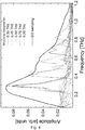
- Fig. 6 illustrates that a desired bandwidth may then be obtained by a properly designed resonant property.
- Fig. 6 illustrates the spectral response of various metallic structures designed for several THz frequencies compared with a spectrum of a THz pulse obtained using electro-optic sampling. The figure illustrates spectral response for metallic structures designed for 0.30, 0.45, 0.60, 0.75 and 0.90 THz.
- Figures 7a and 7b show further optimization of micro-antenna designs.
- Figure 7a examines the case of a dipole antenna, or in other words an I-shaped antenna, and shows calculated length dimensions and spacings or periods for a given desired resonance frequency of the terahertz radiation, and optimized to yield the highest field enhancement.
- a gold antenna having a fixed width of 5 ⁇ m and a fixed thickness of 200nm was assumed.
- the gold forming the antenna was considered to be deposited onto a high resistivity Silicon (HR-SI) substrate.
- HR-SI high resistivity Silicon
- the calculations shown in Figure 7b are performed on a similar system as in Figure 7a , except that a T-shaped antenna was studied. As illustrated, the length of the T top-bar was fixed in the calculations as half the length of the antenna. While these calculations show promising starting points for optimization of antenna layouts for a desired application, micro-antennas of other shapes, dimensions and/or metals may be advantageous for certain applications, e.g. for
- the inventors demonstrated that the response time of the detector is faster than half of the oscillation period of the incoming THz wave. This is advantageous in obtaining an accurate and reliable detector.
- the device does not require cooling. This enables less bulky and less expensive equipment. Also, not requiring cooling provides a more energy efficient apparatus.
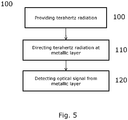
- Fig. 5 is a schematic illustration of steps of a method for detecting terahertz radiation.
- the method comprises a step 100 of providing the terahertz radiation at an input.
- the method comprises a step 110 of directing the terahertz radiation at a metallic layer from the input, wherein metallic layer comprises an arrangement of metallic structures or apertures in the metallic film, the metallic layer emits an optical signal in response to the terahertz radiation.
- the method comprises a step of detecting the emitted optical signal at an optical sensor to provide a signal indicating a property of the terahertz radiation.
- the method may be implemented as software and at least some of the steps executed on a digital processor or the like.
- the invention can be implemented by means of hardware, software, firmware or any combination of these.
- the invention or some of the features thereof can also be implemented as software running on one or more data processors and/or digital signal processors.
- the individual elements of an embodiment of the invention may be physically, functionally and logically implemented in any suitable way such as in a single unit, in a plurality of units or as part of separate functional units.
- the invention may be implemented in a single unit, or be both physically and functionally distributed between different units and processors.
Landscapes
- Physics & Mathematics (AREA)
- Spectroscopy & Molecular Physics (AREA)
- Health & Medical Sciences (AREA)
- General Physics & Mathematics (AREA)
- Life Sciences & Earth Sciences (AREA)
- Chemical & Material Sciences (AREA)
- Analytical Chemistry (AREA)
- Biochemistry (AREA)
- General Health & Medical Sciences (AREA)
- Toxicology (AREA)
- Immunology (AREA)
- Pathology (AREA)
- Investigating Or Analysing Materials By Optical Means (AREA)
Claims (11)
- System (10) zum Erfassen von Terahertzstrahlung, umfassend:einen Eingang, der zum Empfangen der Terahertzstrahlung (20) konfiguriert ist,eine metallische Schicht (30), die zum Empfangen der Terahertzstrahlung von dem Eingang angeordnet ist, und wobei die metallische Schicht eine Anordnung von metallischen Strukturen oder Öffnungen in einem metallischen Film umfasst, wobei die metallische Schicht dazu konfiguriert ist, elektromagnetische Feldverstärkung der Terahertzstrahlung bereitzustellen und somit ein optisches Signal (40) als Reaktion auf die Terahertzstrahlung (20) über einen Prozess aus drei Schritten auszustrahlen, der Terahertz-induzierte Feldemission von Elektronen aus dem Metall, Beschleunigung der Elektronen in dem THz-Feld und Kollision der Elektronen entweder mit Gasmolekülen in der Atmosphäre über dem Metall oder Kollision zwischen den Elektronen und der Metalloberfläche, wenn die Elektronen nach dem Beschleunigungszeitraum zu dem Metall zurückkehren, enthält, wobei UV-VIS-NIR-Licht als ein Ergebnis von nachfolgender Entregung der Gasmoleküle oder Entregung von lokalisierten Oberflächenplasmonen der Metalloberfläche ausgestrahlt wird, undeinen optischen Sensor (50), der dazu angeordnet ist, das ausgestrahlte optische Signal (40) zu erfassen und ein Signal bereitzustellen, das eine Eigenschaft der Terahertzstrahlung (20) angibt.
- System nach Anspruch 1, wobei die metallische Schicht (30) auf einem Substrat (35) angeordnet ist.
- System nach Anspruch 1 oder 2, wobei die metallische Schicht (30) eine Vielzahl von Strukturen oder Öffnungen beinhaltet.
- System nach Anspruch 3, wobei jede der Strukturen eine rechtwinklige Geometrie oder eine T-förmige Geometrie aufweist.
- System nach Anspruch 2, wobei die metallische Schicht (30) auf dem Substrat (35) abgelagert ist und die Struktur während eines Ablagerungsprozesses zufällig gebildet ist.
- System nach einem der Ansprüche 1-5, wobei der Detektor (50) ein Signal ausgibt, das mit der Spitzenfeldstärke des THz-Feldes korreliert.
- Kameravorrichtung, umfassend das System (10) zum Erfassen von Terahertzstrahlung nach einem der vorhergehenden Ansprüche.
- Kameravorrichtung nach Anspruch 7, umfassend eine 2D-Anordnung von Detektoren und optischen Sensoren zum Herstellen einer Reihe von Signalen, die ein 2D-Bild darstellen.
- Verfahren zum Erfassen von Terahertzstrahlung, umfassend die folgenden Schritte:Bereitstellen (100) der Terahertzstrahlung an einem Eingang,Leiten (110) der Terahertzstrahlung an eine metallische Schicht von dem Eingang, wobei die metallische Schicht eine Anordnung von metallischen Strukturen oder Öffnungen in dem metallischen Film umfasst, wobei die metallische Schicht dazu konfiguriert ist, elektromagnetische Feldverstärkung der Terahertzstrahlung bereitzustellen und somit ein optisches Signal als Reaktion auf die Terahertzstrahlung über einen Prozess aus drei Schritten auszustrahlen, der Terahertz-induzierte Feldemission von Elektronen aus dem Metall, Beschleunigung der Elektronen in dem THz-Feld und Kollision der Elektronen entweder mit Gasmolekülen in der Atmosphäre über dem Metall oder Kollision zwischen den Elektronen und der Metalloberfläche, wenn die Elektronen nach dem Beschleunigungszeitraum zu dem Metall zurückkehren, enthält, wobei UV-VIS-NIR-Licht als ein Ergebnis von nachfolgender Entregung der Gasmoleküle oder Entregung von lokalisierten Oberflächenplasmonen der Metalloberfläche ausgestrahlt wird, undErfassen (120) des ausgestrahlten optischen Signals an einem optischen Sensor, um ein Signal bereitzustellen, das eine Eigenschaft der Terahertzstrahlung angibt.
- Verfahren nach Anspruch 9, wobei das Verfahren als ein rechnerimplementiertes Verfahren auf einer Rechenvorrichtung durchgeführt wird.
- Verwendung eines Terahertzstrahlungsdetektors (10) nach einem der Ansprüche 1-8 als ein Gaszusammensetzungssensor, wobei sich das Gaserfassungsverfahren auf Spektralanalyse von ultraviolettem, sichtbarem und Nah-Infrarot (ultraviolet, visible and near-infrared - UV-VIS-NIR)-Licht basiert, das nach Bestrahlung des Terahertzstrahlungsdetektors mit der Terahertzwelle erzeugt wird.
Priority Applications (3)
| Application Number | Priority Date | Filing Date | Title |
|---|---|---|---|
| EP20163305.4A EP3683848B1 (de) | 2013-08-29 | 2014-08-29 | Detektion einer terahertzstrahlung |
| EP14761567.8A EP3039722B1 (de) | 2013-08-29 | 2014-08-29 | Erfassung von terahertzstrahlung |
| DK20163305.4T DK3683848T3 (da) | 2013-08-29 | 2014-08-29 | Detektion af terahertz-stråling |
Applications Claiming Priority (3)
| Application Number | Priority Date | Filing Date | Title |
|---|---|---|---|
| EP13182239 | 2013-08-29 | ||
| PCT/DK2014/050259 WO2015028029A1 (en) | 2013-08-29 | 2014-08-29 | Detection of terahertz radiation |
| EP14761567.8A EP3039722B1 (de) | 2013-08-29 | 2014-08-29 | Erfassung von terahertzstrahlung |
Related Child Applications (1)
| Application Number | Title | Priority Date | Filing Date |
|---|---|---|---|
| EP20163305.4A Division EP3683848B1 (de) | 2013-08-29 | 2014-08-29 | Detektion einer terahertzstrahlung |
Publications (2)
| Publication Number | Publication Date |
|---|---|
| EP3039722A1 EP3039722A1 (de) | 2016-07-06 |
| EP3039722B1 true EP3039722B1 (de) | 2020-03-18 |
Family
ID=49083535
Family Applications (2)
| Application Number | Title | Priority Date | Filing Date |
|---|---|---|---|
| EP14761567.8A Active EP3039722B1 (de) | 2013-08-29 | 2014-08-29 | Erfassung von terahertzstrahlung |
| EP20163305.4A Active EP3683848B1 (de) | 2013-08-29 | 2014-08-29 | Detektion einer terahertzstrahlung |
Family Applications After (1)
| Application Number | Title | Priority Date | Filing Date |
|---|---|---|---|
| EP20163305.4A Active EP3683848B1 (de) | 2013-08-29 | 2014-08-29 | Detektion einer terahertzstrahlung |
Country Status (4)
| Country | Link |
|---|---|
| US (1) | US9983125B2 (de) |
| EP (2) | EP3039722B1 (de) |
| DK (2) | DK3683848T3 (de) |
| WO (1) | WO2015028029A1 (de) |
Families Citing this family (10)
| Publication number | Priority date | Publication date | Assignee | Title |
|---|---|---|---|---|
| US9810578B2 (en) | 2015-03-06 | 2017-11-07 | Massachusetts Institute Of Technology | Systems, methods, and apparatus for radiation detection |
| EP3758040A1 (de) | 2019-06-26 | 2020-12-30 | Technical University of Denmark | Photokathode für ein vakuumsystem |
| EP3758041A1 (de) * | 2019-06-26 | 2020-12-30 | Hamamatsu Photonics K.K. | Elektronenröhre und bildgebungsvorrichtung |
| US11199649B2 (en) * | 2019-08-21 | 2021-12-14 | The United States Of America, As Represented By The Secretary Of The Navy | Metamaterial, focal plane array for broad spectrum imaging |
| DK3863038T3 (da) * | 2020-02-07 | 2022-04-11 | Hamamatsu Photonics Kk | Elektronrør, billeddannelsesindretning og elektromagnetisk bølgedetektionsindretning |
| EP4002418A1 (de) | 2020-11-12 | 2022-05-25 | Hamamatsu Photonics K.K. | Metaflächenelement, elektronenröhre und verfahren zur herstellung einer elektronenröhre |
| US11243161B1 (en) * | 2020-11-20 | 2022-02-08 | Industrial Technology Research Institute | Gas measurement device and gas measurement method |
| EP4135001B1 (de) | 2021-08-10 | 2024-02-28 | Hamamatsu Photonics K.K. | Vorrichtung zur photoelektrischen umwandlung, vorrichtung zur detektion elektromagnetischer wellen, verfahren zur photoelektrischen umwandlung und verfahren zur detektion elektromagnetischer wellen |
| DK4135003T3 (da) | 2021-08-10 | 2025-01-02 | Hamamatsu Photonics Kk | Fotoelektrisk konverteringsindretning, elektromagnetisk bølgedetektionsindretning, fotoelektrisk konverteringsfremgangsmåde og elektromagnetisk bølgedetektionsfremgangsmåde |
| EP4135002B1 (de) | 2021-08-10 | 2024-12-04 | Hamamatsu Photonics K.K. | Photoelektrische umwandlungsvorrichtung und photoelektrisches umwandlungsverfahren |
Family Cites Families (5)
| Publication number | Priority date | Publication date | Assignee | Title |
|---|---|---|---|---|
| WO2000079248A1 (fr) * | 1999-06-21 | 2000-12-28 | Hamamatsu Photonics K.K. | Spectrometre a ondes terahertz |
| JP4476462B2 (ja) * | 2000-03-27 | 2010-06-09 | 株式会社栃木ニコン | 半導体の電気特性評価装置 |
| JP5768429B2 (ja) | 2011-03-23 | 2015-08-26 | セイコーエプソン株式会社 | テラヘルツ波検出装置、テラヘルツ波長フィルター、イメージング装置および計測装置 |
| US9106342B2 (en) * | 2011-05-03 | 2015-08-11 | William Marsh Rice University | Device and method for modulating transmission of terahertz waves |
| JP5910064B2 (ja) | 2011-12-20 | 2016-04-27 | セイコーエプソン株式会社 | 光伝導アンテナ、テラヘルツ波発生装置、カメラ、イメージング装置および計測装置 |
-
2014
- 2014-08-29 DK DK20163305.4T patent/DK3683848T3/da active
- 2014-08-29 WO PCT/DK2014/050259 patent/WO2015028029A1/en not_active Ceased
- 2014-08-29 EP EP14761567.8A patent/EP3039722B1/de active Active
- 2014-08-29 EP EP20163305.4A patent/EP3683848B1/de active Active
- 2014-08-29 US US14/915,473 patent/US9983125B2/en active Active
- 2014-08-29 DK DK14761567.8T patent/DK3039722T3/da active
Non-Patent Citations (1)
| Title |
|---|
| None * |
Also Published As
| Publication number | Publication date |
|---|---|
| US9983125B2 (en) | 2018-05-29 |
| EP3039722A1 (de) | 2016-07-06 |
| DK3683848T3 (da) | 2022-09-05 |
| US20160216201A1 (en) | 2016-07-28 |
| EP3683848A1 (de) | 2020-07-22 |
| EP3683848B1 (de) | 2022-06-29 |
| WO2015028029A1 (en) | 2015-03-05 |
| DK3039722T3 (da) | 2020-05-11 |
Similar Documents
| Publication | Publication Date | Title |
|---|---|---|
| EP3039722B1 (de) | Erfassung von terahertzstrahlung | |
| Malhotra et al. | Terahertz antenna technology for imaging applications: A technical review | |
| US10753867B2 (en) | System and method for identifying materials using a THz spectral fingerprint in a media with high water content | |
| Baker et al. | Detection of concealed explosives at a distance using terahertz technology | |
| Zhou et al. | Multicolor T‐ray imaging using multispectral metamaterials | |
| US9494464B2 (en) | Terahertz imaging devices and systems, and related methods, for detection of materials | |
| US10024723B2 (en) | Detection of electromagnetic radiation using nonlinear materials | |
| Grant et al. | A monolithic resonant terahertz sensor element comprising a metamaterial absorber and micro‐bolometer | |
| NL2005856C2 (en) | Terahertz radiation detection using micro-plasma. | |
| US9071776B2 (en) | Reflective imaging device and image acquisition method | |
| JP2008145289A (ja) | 電磁波センサ、撮像素子及び撮像装置 | |
| Stenger et al. | Thin film lithium tantalate (TFLT) pyroelectric detectors | |
| EP3106858B1 (de) | Ferninfrarot-bildgebungsvorrichtung und ferninfrarot-bildgebungsverfahren | |
| Angrisani et al. | THz measurement systems | |
| Smith et al. | Enhanced performance of VOx-based bolometer using patterned gold black absorber | |
| Lucyszyn et al. | Technology demonstrators for low-cost terahertz engineering | |
| JP2007316044A (ja) | フォトキャパシタンス法を用いたテラヘルツ光センシングシステム | |
| Jokubauskis | Development and applications of compact spectroscopic terahertz imaging systems using principles of optical beam engineering | |
| Malhotra et al. | Analysis, design and characterization of small-gap photoconductive dipole antenna for terahertz imaging applications | |
| Aji | Study on Terahertz Bolometer with High-Impedance Antenna | |
| Simoens et al. | Development of uncooled antenna-coupled microbolometer arrays for explosive detection and identification | |
| Dégardin et al. | Fast thermal detectors: migrating from the NIR to the terahertz waves | |
| Henri et al. | 8 x 8 Terahertz Photoconductive Antenna Array and Parallelized Signal Acquisition System for Fast Spatially Resolved Time Domain Spectroscopy | |
| Henri | Characterization of an 8 x 8 Terahertz Photoconductive Antenna Array for Spatially Resolved Time-domain Spectroscopy and Imaging Applications | |
| Gritz et al. | Direct detection antenna-coupled mmW sensors for the detection of explosive vapors |
Legal Events
| Date | Code | Title | Description |
|---|---|---|---|
| PUAI | Public reference made under article 153(3) epc to a published international application that has entered the european phase |
Free format text: ORIGINAL CODE: 0009012 |
|
| 17P | Request for examination filed |
Effective date: 20160329 |
|
| AK | Designated contracting states |
Kind code of ref document: A1 Designated state(s): AL AT BE BG CH CY CZ DE DK EE ES FI FR GB GR HR HU IE IS IT LI LT LU LV MC MK MT NL NO PL PT RO RS SE SI SK SM TR |
|
| AX | Request for extension of the european patent |
Extension state: BA ME |
|
| DAX | Request for extension of the european patent (deleted) | ||
| STAA | Information on the status of an ep patent application or granted ep patent |
Free format text: STATUS: EXAMINATION IS IN PROGRESS |
|
| 17Q | First examination report despatched |
Effective date: 20180621 |
|
| GRAP | Despatch of communication of intention to grant a patent |
Free format text: ORIGINAL CODE: EPIDOSNIGR1 |
|
| STAA | Information on the status of an ep patent application or granted ep patent |
Free format text: STATUS: GRANT OF PATENT IS INTENDED |
|
| INTG | Intention to grant announced |
Effective date: 20191001 |
|
| RIN1 | Information on inventor provided before grant (corrected) |
Inventor name: JEPSEN, PETER UHD Inventor name: IWASZCZUK, KRZYSZTOF |
|
| RAP1 | Party data changed (applicant data changed or rights of an application transferred) |
Owner name: HAMAMATSU PHOTONICS K.K. |
|
| GRAS | Grant fee paid |
Free format text: ORIGINAL CODE: EPIDOSNIGR3 |
|
| GRAA | (expected) grant |
Free format text: ORIGINAL CODE: 0009210 |
|
| STAA | Information on the status of an ep patent application or granted ep patent |
Free format text: STATUS: THE PATENT HAS BEEN GRANTED |
|
| AK | Designated contracting states |
Kind code of ref document: B1 Designated state(s): AL AT BE BG CH CY CZ DE DK EE ES FI FR GB GR HR HU IE IS IT LI LT LU LV MC MK MT NL NO PL PT RO RS SE SI SK SM TR |
|
| REG | Reference to a national code |
Ref country code: GB Ref legal event code: FG4D |
|
| REG | Reference to a national code |
Ref country code: DE Ref legal event code: R096 Ref document number: 602014062529 Country of ref document: DE |
|
| REG | Reference to a national code |
Ref country code: AT Ref legal event code: REF Ref document number: 1246920 Country of ref document: AT Kind code of ref document: T Effective date: 20200415 Ref country code: IE Ref legal event code: FG4D |
|
| REG | Reference to a national code |
Ref country code: DK Ref legal event code: T3 Effective date: 20200507 |
|
| PG25 | Lapsed in a contracting state [announced via postgrant information from national office to epo] |
Ref country code: NO Free format text: LAPSE BECAUSE OF FAILURE TO SUBMIT A TRANSLATION OF THE DESCRIPTION OR TO PAY THE FEE WITHIN THE PRESCRIBED TIME-LIMIT Effective date: 20200618 Ref country code: FI Free format text: LAPSE BECAUSE OF FAILURE TO SUBMIT A TRANSLATION OF THE DESCRIPTION OR TO PAY THE FEE WITHIN THE PRESCRIBED TIME-LIMIT Effective date: 20200318 Ref country code: RS Free format text: LAPSE BECAUSE OF FAILURE TO SUBMIT A TRANSLATION OF THE DESCRIPTION OR TO PAY THE FEE WITHIN THE PRESCRIBED TIME-LIMIT Effective date: 20200318 |
|
| REG | Reference to a national code |
Ref country code: NL Ref legal event code: MP Effective date: 20200318 |
|
| PG25 | Lapsed in a contracting state [announced via postgrant information from national office to epo] |
Ref country code: LV Free format text: LAPSE BECAUSE OF FAILURE TO SUBMIT A TRANSLATION OF THE DESCRIPTION OR TO PAY THE FEE WITHIN THE PRESCRIBED TIME-LIMIT Effective date: 20200318 Ref country code: SE Free format text: LAPSE BECAUSE OF FAILURE TO SUBMIT A TRANSLATION OF THE DESCRIPTION OR TO PAY THE FEE WITHIN THE PRESCRIBED TIME-LIMIT Effective date: 20200318 Ref country code: HR Free format text: LAPSE BECAUSE OF FAILURE TO SUBMIT A TRANSLATION OF THE DESCRIPTION OR TO PAY THE FEE WITHIN THE PRESCRIBED TIME-LIMIT Effective date: 20200318 Ref country code: BG Free format text: LAPSE BECAUSE OF FAILURE TO SUBMIT A TRANSLATION OF THE DESCRIPTION OR TO PAY THE FEE WITHIN THE PRESCRIBED TIME-LIMIT Effective date: 20200618 Ref country code: GR Free format text: LAPSE BECAUSE OF FAILURE TO SUBMIT A TRANSLATION OF THE DESCRIPTION OR TO PAY THE FEE WITHIN THE PRESCRIBED TIME-LIMIT Effective date: 20200619 |
|
| REG | Reference to a national code |
Ref country code: LT Ref legal event code: MG4D |
|
| PG25 | Lapsed in a contracting state [announced via postgrant information from national office to epo] |
Ref country code: NL Free format text: LAPSE BECAUSE OF FAILURE TO SUBMIT A TRANSLATION OF THE DESCRIPTION OR TO PAY THE FEE WITHIN THE PRESCRIBED TIME-LIMIT Effective date: 20200318 |
|
| PG25 | Lapsed in a contracting state [announced via postgrant information from national office to epo] |
Ref country code: SK Free format text: LAPSE BECAUSE OF FAILURE TO SUBMIT A TRANSLATION OF THE DESCRIPTION OR TO PAY THE FEE WITHIN THE PRESCRIBED TIME-LIMIT Effective date: 20200318 Ref country code: SM Free format text: LAPSE BECAUSE OF FAILURE TO SUBMIT A TRANSLATION OF THE DESCRIPTION OR TO PAY THE FEE WITHIN THE PRESCRIBED TIME-LIMIT Effective date: 20200318 Ref country code: EE Free format text: LAPSE BECAUSE OF FAILURE TO SUBMIT A TRANSLATION OF THE DESCRIPTION OR TO PAY THE FEE WITHIN THE PRESCRIBED TIME-LIMIT Effective date: 20200318 Ref country code: PT Free format text: LAPSE BECAUSE OF FAILURE TO SUBMIT A TRANSLATION OF THE DESCRIPTION OR TO PAY THE FEE WITHIN THE PRESCRIBED TIME-LIMIT Effective date: 20200812 Ref country code: LT Free format text: LAPSE BECAUSE OF FAILURE TO SUBMIT A TRANSLATION OF THE DESCRIPTION OR TO PAY THE FEE WITHIN THE PRESCRIBED TIME-LIMIT Effective date: 20200318 Ref country code: RO Free format text: LAPSE BECAUSE OF FAILURE TO SUBMIT A TRANSLATION OF THE DESCRIPTION OR TO PAY THE FEE WITHIN THE PRESCRIBED TIME-LIMIT Effective date: 20200318 Ref country code: CZ Free format text: LAPSE BECAUSE OF FAILURE TO SUBMIT A TRANSLATION OF THE DESCRIPTION OR TO PAY THE FEE WITHIN THE PRESCRIBED TIME-LIMIT Effective date: 20200318 Ref country code: IS Free format text: LAPSE BECAUSE OF FAILURE TO SUBMIT A TRANSLATION OF THE DESCRIPTION OR TO PAY THE FEE WITHIN THE PRESCRIBED TIME-LIMIT Effective date: 20200718 |
|
| REG | Reference to a national code |
Ref country code: AT Ref legal event code: MK05 Ref document number: 1246920 Country of ref document: AT Kind code of ref document: T Effective date: 20200318 |
|
| REG | Reference to a national code |
Ref country code: DE Ref legal event code: R097 Ref document number: 602014062529 Country of ref document: DE |
|
| PLBE | No opposition filed within time limit |
Free format text: ORIGINAL CODE: 0009261 |
|
| STAA | Information on the status of an ep patent application or granted ep patent |
Free format text: STATUS: NO OPPOSITION FILED WITHIN TIME LIMIT |
|
| PG25 | Lapsed in a contracting state [announced via postgrant information from national office to epo] |
Ref country code: ES Free format text: LAPSE BECAUSE OF FAILURE TO SUBMIT A TRANSLATION OF THE DESCRIPTION OR TO PAY THE FEE WITHIN THE PRESCRIBED TIME-LIMIT Effective date: 20200318 Ref country code: AT Free format text: LAPSE BECAUSE OF FAILURE TO SUBMIT A TRANSLATION OF THE DESCRIPTION OR TO PAY THE FEE WITHIN THE PRESCRIBED TIME-LIMIT Effective date: 20200318 Ref country code: IT Free format text: LAPSE BECAUSE OF FAILURE TO SUBMIT A TRANSLATION OF THE DESCRIPTION OR TO PAY THE FEE WITHIN THE PRESCRIBED TIME-LIMIT Effective date: 20200318 |
|
| 26N | No opposition filed |
Effective date: 20201221 |
|
| PG25 | Lapsed in a contracting state [announced via postgrant information from national office to epo] |
Ref country code: PL Free format text: LAPSE BECAUSE OF FAILURE TO SUBMIT A TRANSLATION OF THE DESCRIPTION OR TO PAY THE FEE WITHIN THE PRESCRIBED TIME-LIMIT Effective date: 20200318 |
|
| PG25 | Lapsed in a contracting state [announced via postgrant information from national office to epo] |
Ref country code: MC Free format text: LAPSE BECAUSE OF FAILURE TO SUBMIT A TRANSLATION OF THE DESCRIPTION OR TO PAY THE FEE WITHIN THE PRESCRIBED TIME-LIMIT Effective date: 20200318 |
|
| PG25 | Lapsed in a contracting state [announced via postgrant information from national office to epo] |
Ref country code: LU Free format text: LAPSE BECAUSE OF NON-PAYMENT OF DUE FEES Effective date: 20200829 |
|
| REG | Reference to a national code |
Ref country code: BE Ref legal event code: MM Effective date: 20200831 |
|
| PG25 | Lapsed in a contracting state [announced via postgrant information from national office to epo] |
Ref country code: SI Free format text: LAPSE BECAUSE OF FAILURE TO SUBMIT A TRANSLATION OF THE DESCRIPTION OR TO PAY THE FEE WITHIN THE PRESCRIBED TIME-LIMIT Effective date: 20200318 |
|
| PG25 | Lapsed in a contracting state [announced via postgrant information from national office to epo] |
Ref country code: BE Free format text: LAPSE BECAUSE OF NON-PAYMENT OF DUE FEES Effective date: 20200831 Ref country code: IE Free format text: LAPSE BECAUSE OF NON-PAYMENT OF DUE FEES Effective date: 20200829 |
|
| PG25 | Lapsed in a contracting state [announced via postgrant information from national office to epo] |
Ref country code: TR Free format text: LAPSE BECAUSE OF FAILURE TO SUBMIT A TRANSLATION OF THE DESCRIPTION OR TO PAY THE FEE WITHIN THE PRESCRIBED TIME-LIMIT Effective date: 20200318 Ref country code: MT Free format text: LAPSE BECAUSE OF FAILURE TO SUBMIT A TRANSLATION OF THE DESCRIPTION OR TO PAY THE FEE WITHIN THE PRESCRIBED TIME-LIMIT Effective date: 20200318 Ref country code: CY Free format text: LAPSE BECAUSE OF FAILURE TO SUBMIT A TRANSLATION OF THE DESCRIPTION OR TO PAY THE FEE WITHIN THE PRESCRIBED TIME-LIMIT Effective date: 20200318 |
|
| PG25 | Lapsed in a contracting state [announced via postgrant information from national office to epo] |
Ref country code: MK Free format text: LAPSE BECAUSE OF FAILURE TO SUBMIT A TRANSLATION OF THE DESCRIPTION OR TO PAY THE FEE WITHIN THE PRESCRIBED TIME-LIMIT Effective date: 20200318 Ref country code: AL Free format text: LAPSE BECAUSE OF FAILURE TO SUBMIT A TRANSLATION OF THE DESCRIPTION OR TO PAY THE FEE WITHIN THE PRESCRIBED TIME-LIMIT Effective date: 20200318 |
|
| P01 | Opt-out of the competence of the unified patent court (upc) registered |
Effective date: 20230509 |
|
| REG | Reference to a national code |
Ref country code: DE Ref legal event code: R079 Ref document number: 602014062529 Country of ref document: DE Free format text: PREVIOUS MAIN CLASS: H01L0031023200 Ipc: H10F0077400000 |
|
| PGFP | Annual fee paid to national office [announced via postgrant information from national office to epo] |
Ref country code: DK Payment date: 20250814 Year of fee payment: 12 Ref country code: DE Payment date: 20250702 Year of fee payment: 12 |
|
| PGFP | Annual fee paid to national office [announced via postgrant information from national office to epo] |
Ref country code: GB Payment date: 20250703 Year of fee payment: 12 |
|
| PGFP | Annual fee paid to national office [announced via postgrant information from national office to epo] |
Ref country code: FR Payment date: 20250703 Year of fee payment: 12 |
|
| PGFP | Annual fee paid to national office [announced via postgrant information from national office to epo] |
Ref country code: CH Payment date: 20250901 Year of fee payment: 12 |