EP3039718B1 - Partly-transparent thin-film solar module - Google Patents
Partly-transparent thin-film solar module Download PDFInfo
- Publication number
- EP3039718B1 EP3039718B1 EP14777014.3A EP14777014A EP3039718B1 EP 3039718 B1 EP3039718 B1 EP 3039718B1 EP 14777014 A EP14777014 A EP 14777014A EP 3039718 B1 EP3039718 B1 EP 3039718B1
- Authority
- EP
- European Patent Office
- Prior art keywords
- transparent
- solar cell
- contact layer
- surface regions
- structuring
- Prior art date
- Legal status (The legal status is an assumption and is not a legal conclusion. Google has not performed a legal analysis and makes no representation as to the accuracy of the status listed.)
- Active
Links
- 239000010409 thin film Substances 0.000 title description 31
- 238000000034 method Methods 0.000 claims description 28
- 239000004065 semiconductor Substances 0.000 claims description 9
- 239000000758 substrate Substances 0.000 claims description 8
- 229920003023 plastic Polymers 0.000 claims description 5
- 238000000151 deposition Methods 0.000 claims description 3
- 238000004519 manufacturing process Methods 0.000 claims description 3
- 239000011248 coating agent Substances 0.000 claims description 2
- 238000000576 coating method Methods 0.000 claims description 2
- 238000005488 sandblasting Methods 0.000 claims description 2
- 238000005530 etching Methods 0.000 claims 1
- 239000010410 layer Substances 0.000 description 51
- 230000000694 effects Effects 0.000 description 6
- 239000011521 glass Substances 0.000 description 6
- 239000000463 material Substances 0.000 description 4
- 229910004613 CdTe Inorganic materials 0.000 description 3
- 239000004033 plastic Substances 0.000 description 3
- 230000000717 retained effect Effects 0.000 description 3
- XLOMVQKBTHCTTD-UHFFFAOYSA-N Zinc monoxide Chemical compound [Zn]=O XLOMVQKBTHCTTD-UHFFFAOYSA-N 0.000 description 2
- 229910021417 amorphous silicon Inorganic materials 0.000 description 2
- 238000005253 cladding Methods 0.000 description 2
- 230000008021 deposition Effects 0.000 description 2
- 238000010297 mechanical methods and process Methods 0.000 description 2
- 230000005226 mechanical processes and functions Effects 0.000 description 2
- KTSFMFGEAAANTF-UHFFFAOYSA-N [Cu].[Se].[Se].[In] Chemical compound [Cu].[Se].[Se].[In] KTSFMFGEAAANTF-UHFFFAOYSA-N 0.000 description 1
- 230000005540 biological transmission Effects 0.000 description 1
- 229910052793 cadmium Inorganic materials 0.000 description 1
- FJZMJOPKABSQOK-UHFFFAOYSA-N cadmium(2+) disulfide Chemical compound [S--].[S--].[Cd++].[Cd++] FJZMJOPKABSQOK-UHFFFAOYSA-N 0.000 description 1
- 238000004364 calculation method Methods 0.000 description 1
- 238000006243 chemical reaction Methods 0.000 description 1
- 150000001875 compounds Chemical class 0.000 description 1
- 239000004020 conductor Substances 0.000 description 1
- 229910003437 indium oxide Inorganic materials 0.000 description 1
- PJXISJQVUVHSOJ-UHFFFAOYSA-N indium(iii) oxide Chemical compound [O-2].[O-2].[O-2].[In+3].[In+3] PJXISJQVUVHSOJ-UHFFFAOYSA-N 0.000 description 1
- 239000011810 insulating material Substances 0.000 description 1
- 230000010354 integration Effects 0.000 description 1
- 238000003475 lamination Methods 0.000 description 1
- 230000007246 mechanism Effects 0.000 description 1
- 229910052751 metal Inorganic materials 0.000 description 1
- 239000002184 metal Substances 0.000 description 1
- 230000035699 permeability Effects 0.000 description 1
- 229920003229 poly(methyl methacrylate) Polymers 0.000 description 1
- 239000004926 polymethyl methacrylate Substances 0.000 description 1
- 239000011241 protective layer Substances 0.000 description 1
- 230000003595 spectral effect Effects 0.000 description 1
- 229940071182 stannate Drugs 0.000 description 1
- XOLBLPGZBRYERU-UHFFFAOYSA-N tin dioxide Chemical compound O=[Sn]=O XOLBLPGZBRYERU-UHFFFAOYSA-N 0.000 description 1
- 229910001887 tin oxide Inorganic materials 0.000 description 1
- 230000000007 visual effect Effects 0.000 description 1
- 239000011787 zinc oxide Substances 0.000 description 1
Images


Classifications
-
- H—ELECTRICITY
- H01—ELECTRIC ELEMENTS
- H01L—SEMICONDUCTOR DEVICES NOT COVERED BY CLASS H10
- H01L31/00—Semiconductor devices sensitive to infrared radiation, light, electromagnetic radiation of shorter wavelength or corpuscular radiation and specially adapted either for the conversion of the energy of such radiation into electrical energy or for the control of electrical energy by such radiation; Processes or apparatus specially adapted for the manufacture or treatment thereof or of parts thereof; Details thereof
- H01L31/04—Semiconductor devices sensitive to infrared radiation, light, electromagnetic radiation of shorter wavelength or corpuscular radiation and specially adapted either for the conversion of the energy of such radiation into electrical energy or for the control of electrical energy by such radiation; Processes or apparatus specially adapted for the manufacture or treatment thereof or of parts thereof; Details thereof adapted as photovoltaic [PV] conversion devices
- H01L31/042—PV modules or arrays of single PV cells
- H01L31/0445—PV modules or arrays of single PV cells including thin film solar cells, e.g. single thin film a-Si, CIS or CdTe solar cells
- H01L31/046—PV modules composed of a plurality of thin film solar cells deposited on the same substrate
- H01L31/0468—PV modules composed of a plurality of thin film solar cells deposited on the same substrate comprising specific means for obtaining partial light transmission through the module, e.g. partially transparent thin film solar modules for windows
-
- H—ELECTRICITY
- H01—ELECTRIC ELEMENTS
- H01L—SEMICONDUCTOR DEVICES NOT COVERED BY CLASS H10
- H01L31/00—Semiconductor devices sensitive to infrared radiation, light, electromagnetic radiation of shorter wavelength or corpuscular radiation and specially adapted either for the conversion of the energy of such radiation into electrical energy or for the control of electrical energy by such radiation; Processes or apparatus specially adapted for the manufacture or treatment thereof or of parts thereof; Details thereof
- H01L31/0248—Semiconductor devices sensitive to infrared radiation, light, electromagnetic radiation of shorter wavelength or corpuscular radiation and specially adapted either for the conversion of the energy of such radiation into electrical energy or for the control of electrical energy by such radiation; Processes or apparatus specially adapted for the manufacture or treatment thereof or of parts thereof; Details thereof characterised by their semiconductor bodies
- H01L31/0352—Semiconductor devices sensitive to infrared radiation, light, electromagnetic radiation of shorter wavelength or corpuscular radiation and specially adapted either for the conversion of the energy of such radiation into electrical energy or for the control of electrical energy by such radiation; Processes or apparatus specially adapted for the manufacture or treatment thereof or of parts thereof; Details thereof characterised by their semiconductor bodies characterised by their shape or by the shapes, relative sizes or disposition of the semiconductor regions
-
- H—ELECTRICITY
- H01—ELECTRIC ELEMENTS
- H01L—SEMICONDUCTOR DEVICES NOT COVERED BY CLASS H10
- H01L31/00—Semiconductor devices sensitive to infrared radiation, light, electromagnetic radiation of shorter wavelength or corpuscular radiation and specially adapted either for the conversion of the energy of such radiation into electrical energy or for the control of electrical energy by such radiation; Processes or apparatus specially adapted for the manufacture or treatment thereof or of parts thereof; Details thereof
- H01L31/04—Semiconductor devices sensitive to infrared radiation, light, electromagnetic radiation of shorter wavelength or corpuscular radiation and specially adapted either for the conversion of the energy of such radiation into electrical energy or for the control of electrical energy by such radiation; Processes or apparatus specially adapted for the manufacture or treatment thereof or of parts thereof; Details thereof adapted as photovoltaic [PV] conversion devices
- H01L31/042—PV modules or arrays of single PV cells
- H01L31/0445—PV modules or arrays of single PV cells including thin film solar cells, e.g. single thin film a-Si, CIS or CdTe solar cells
- H01L31/046—PV modules composed of a plurality of thin film solar cells deposited on the same substrate
- H01L31/0463—PV modules composed of a plurality of thin film solar cells deposited on the same substrate characterised by special patterning methods to connect the PV cells in a module, e.g. laser cutting of the conductive or active layers
-
- H—ELECTRICITY
- H01—ELECTRIC ELEMENTS
- H01L—SEMICONDUCTOR DEVICES NOT COVERED BY CLASS H10
- H01L31/00—Semiconductor devices sensitive to infrared radiation, light, electromagnetic radiation of shorter wavelength or corpuscular radiation and specially adapted either for the conversion of the energy of such radiation into electrical energy or for the control of electrical energy by such radiation; Processes or apparatus specially adapted for the manufacture or treatment thereof or of parts thereof; Details thereof
- H01L31/02—Details
- H01L31/0224—Electrodes
- H01L31/022408—Electrodes for devices characterised by at least one potential jump barrier or surface barrier
- H01L31/022425—Electrodes for devices characterised by at least one potential jump barrier or surface barrier for solar cells
- H01L31/022441—Electrode arrangements specially adapted for back-contact solar cells
-
- H—ELECTRICITY
- H01—ELECTRIC ELEMENTS
- H01L—SEMICONDUCTOR DEVICES NOT COVERED BY CLASS H10
- H01L31/00—Semiconductor devices sensitive to infrared radiation, light, electromagnetic radiation of shorter wavelength or corpuscular radiation and specially adapted either for the conversion of the energy of such radiation into electrical energy or for the control of electrical energy by such radiation; Processes or apparatus specially adapted for the manufacture or treatment thereof or of parts thereof; Details thereof
- H01L31/04—Semiconductor devices sensitive to infrared radiation, light, electromagnetic radiation of shorter wavelength or corpuscular radiation and specially adapted either for the conversion of the energy of such radiation into electrical energy or for the control of electrical energy by such radiation; Processes or apparatus specially adapted for the manufacture or treatment thereof or of parts thereof; Details thereof adapted as photovoltaic [PV] conversion devices
- H01L31/042—PV modules or arrays of single PV cells
- H01L31/048—Encapsulation of modules
- H01L31/0481—Encapsulation of modules characterised by the composition of the encapsulation material
-
- H—ELECTRICITY
- H01—ELECTRIC ELEMENTS
- H01L—SEMICONDUCTOR DEVICES NOT COVERED BY CLASS H10
- H01L31/00—Semiconductor devices sensitive to infrared radiation, light, electromagnetic radiation of shorter wavelength or corpuscular radiation and specially adapted either for the conversion of the energy of such radiation into electrical energy or for the control of electrical energy by such radiation; Processes or apparatus specially adapted for the manufacture or treatment thereof or of parts thereof; Details thereof
- H01L31/04—Semiconductor devices sensitive to infrared radiation, light, electromagnetic radiation of shorter wavelength or corpuscular radiation and specially adapted either for the conversion of the energy of such radiation into electrical energy or for the control of electrical energy by such radiation; Processes or apparatus specially adapted for the manufacture or treatment thereof or of parts thereof; Details thereof adapted as photovoltaic [PV] conversion devices
- H01L31/042—PV modules or arrays of single PV cells
- H01L31/048—Encapsulation of modules
- H01L31/0488—Double glass encapsulation, e.g. photovoltaic cells arranged between front and rear glass sheets
-
- H—ELECTRICITY
- H01—ELECTRIC ELEMENTS
- H01L—SEMICONDUCTOR DEVICES NOT COVERED BY CLASS H10
- H01L31/00—Semiconductor devices sensitive to infrared radiation, light, electromagnetic radiation of shorter wavelength or corpuscular radiation and specially adapted either for the conversion of the energy of such radiation into electrical energy or for the control of electrical energy by such radiation; Processes or apparatus specially adapted for the manufacture or treatment thereof or of parts thereof; Details thereof
- H01L31/04—Semiconductor devices sensitive to infrared radiation, light, electromagnetic radiation of shorter wavelength or corpuscular radiation and specially adapted either for the conversion of the energy of such radiation into electrical energy or for the control of electrical energy by such radiation; Processes or apparatus specially adapted for the manufacture or treatment thereof or of parts thereof; Details thereof adapted as photovoltaic [PV] conversion devices
- H01L31/042—PV modules or arrays of single PV cells
- H01L31/05—Electrical interconnection means between PV cells inside the PV module, e.g. series connection of PV cells
- H01L31/0504—Electrical interconnection means between PV cells inside the PV module, e.g. series connection of PV cells specially adapted for series or parallel connection of solar cells in a module
- H01L31/0516—Electrical interconnection means between PV cells inside the PV module, e.g. series connection of PV cells specially adapted for series or parallel connection of solar cells in a module specially adapted for interconnection of back-contact solar cells
-
- H—ELECTRICITY
- H01—ELECTRIC ELEMENTS
- H01L—SEMICONDUCTOR DEVICES NOT COVERED BY CLASS H10
- H01L31/00—Semiconductor devices sensitive to infrared radiation, light, electromagnetic radiation of shorter wavelength or corpuscular radiation and specially adapted either for the conversion of the energy of such radiation into electrical energy or for the control of electrical energy by such radiation; Processes or apparatus specially adapted for the manufacture or treatment thereof or of parts thereof; Details thereof
- H01L31/18—Processes or apparatus specially adapted for the manufacture or treatment of these devices or of parts thereof
-
- Y—GENERAL TAGGING OF NEW TECHNOLOGICAL DEVELOPMENTS; GENERAL TAGGING OF CROSS-SECTIONAL TECHNOLOGIES SPANNING OVER SEVERAL SECTIONS OF THE IPC; TECHNICAL SUBJECTS COVERED BY FORMER USPC CROSS-REFERENCE ART COLLECTIONS [XRACs] AND DIGESTS
- Y02—TECHNOLOGIES OR APPLICATIONS FOR MITIGATION OR ADAPTATION AGAINST CLIMATE CHANGE
- Y02E—REDUCTION OF GREENHOUSE GAS [GHG] EMISSIONS, RELATED TO ENERGY GENERATION, TRANSMISSION OR DISTRIBUTION
- Y02E10/00—Energy generation through renewable energy sources
- Y02E10/50—Photovoltaic [PV] energy
Definitions
- the invention relates to thin-film solar modules in which a desired partial transparency for the incident light is achieved by deliberately removing certain parts of the non-or only very weakly transparent, photovoltaically active surface.
- transparency is understood to mean the permeability to light in the visible spectral range (380 nm to 780 nm), based on the entire area examined. This means explicitly that the area examined (e.g. a solar module) can have areas that are highly opaque or even completely opaque and more translucent. In this context, partial transparency means that the surface under consideration is transparent to part of the incident light.
- Solar cells will play an important role in future energy generation.
- Thin-film solar modules in particular have advantages in terms of low material consumption and easier mass production.
- Such solar modules are constructed from amorphous or polycrystalline semiconductor materials which can be deposited inexpensively on large-area substrates, in particular glass substrates.
- the most important representatives are solar modules based on cadmium sulfide-cadmium telluride (CdS / CdTe), copper indium diselenide (CIS-CIGS) or amorphous silicon (a-Si).
- Thin-film solar modules consist of several layers that are successively deposited on the substrate and possibly further treated.
- the transparent front contact layer, the non-or only very weakly transparent, photovoltaically active semiconductor layers and the back contact layer are deposited from the substrate (usually glass).
- the back contact layer is not transparent.
- designs with transparent back contact layers are also known.
- the generally non-transparent back contact layer, the non-transparent, photovoltaically active semiconductor layers and the transparent front contact layer are deposited from the substrate.
- the front contact layer usually contains transparent conductive oxides (TCO, transparent conductive oxide), e.g. tin-doped indium oxide (ITO), fluorine-doped tin oxide (FTO) or aluminum-doped zinc oxide (AZO) as well as stannate-like compounds, e.g. cadmium stannate (Cd 2 (SnO 4 )), to use.
- TCO transparent conductive oxides
- ITO tin-doped indium oxide
- FTO fluorine-doped tin oxide
- AZO aluminum-doped zinc oxide
- stannate-like compounds e.g. cadmium stannate (Cd 2 (SnO 4 )
- the photovoltaic conversion of solar energy into electrical energy typically causes voltages of less than 1 volt in the state of the art solar cells.
- several individual solar cells must therefore be connected in series.
- this is preferably done by dividing the active area of the solar module into individual, strip-shaped solar cells. The division is made by so-called structuring strips, each structuring strip preferably consisting of three closely adjacent structuring cuts.
- each partial section cuts through only certain individual layers of the layer sequence of the solar module.
- a suitable arrangement of the partial cuts with respect to one another and, if appropriate, suitable filling of the structuring cuts with conductive or insulating material ensures that the back contact of the one solar cell comes into contact with the front contact layer of the subsequent solar cell and the front and back contacts are cut in front of or behind the contact point , which results in the serial connection of these solar cells.
- This process is also called structuring.
- a thin-film solar module according to the prior art has a plurality of individual solar cells, which preferably extend from one edge to the other edge of the solar module (or to the stripped edges of the solar module).
- the individual strip-shaped solar cells are separated from one another by the structuring strips and connected in series with one another.
- Various methods for structuring are known from the prior art, in which the coating in the area of the structuring strips in the form of individual structuring cuts is generally removed in whole or in part. These are, for example, mechanical processes, laser processing processes, paste writing methods or lift-off techniques (cf. DE 37 12 589 A1 and DE 43 24 318 C1 ).
- the structuring strips preferably run parallel to one another.
- An essential aspect of photovoltaic energy generation is the space required to set up the solar modules. From an economic-ecological point of view, the elevation of the solar modules on roofs and the integration of the solar modules in building facades, especially high-rise facades, are particularly desirable.
- solar modules are designed so that they can perform the function of a typical facade cladding.
- they advantageously produce electrical energy that can be used in the home or fed into the public electrical network.
- Facades especially high-rise facades, are generally subject to special architectural requirements.
- areas of the facade cladding are to be made partially transparent. Even if the facade area does not contain a window, but only in front of a functional room that does not require direct daylight, a certain amount of light may still be desirable.
- Partially transparent facade elements can be advantageous here.
- the US 4,795,500 A. describes a thin film solar module made in the Superstrat configuration described above. After the deposition of the metal back electrode, holes are etched in the back electrode or in the back electrode and the photovoltaically active semiconductor layers in order to increase the transparency of the solar module. The back of the solar module is then closed with a transparent protective layer, for example made of plastic.
- the object is achieved by producing a partial transparency of the solar module by deliberately removing freely definable surface areas (transparent surface areas) of the layer stack of the thin-film solar cell of such a module in a thin-film solar module using a suitable method, preferably before lamination.
- the freely definable surface areas are preferably designed in such a way that the free areas extend at least through all non-transparent layers, so that a type of window is created in the layer stack of the solar cell through which the light can pass.
- the solar module produced by the method according to the invention has a plurality of freely definable surface areas which do not contain a layer stack or only light-permeable layers of the layer stack.
- the area proportion of the freely definable area areas is preferably between 70% and 5%, particularly preferably between 50% and 10% and very particularly preferably between 40% and 20% of the total area of the solar module. An area share of 30% + -5% has proven to be particularly advantageous.
- the freely definable surface areas are formed by removing all layers of the layer stack, but at least the opaque layers of the layer stack, at each location provided for a surface area.
- the subsequent removal of the layer stack of the thin-film solar cell in the defined surface areas is preferably carried out using a laser method, as is also used in the structuring task of the thin-film module. Also preferred are the mechanical processes mentioned above using gravers and sandblasting effects or special lift-off mechanisms and adapted photolithographic processes.
- the freely definable surface areas are formed by restricting the deposition of all layers of the layer stack, but at least of the opaque layers, to the regions outside the freely definable surface areas.
- Technical precautions from the prior art, such as masks, are suitable for this. With this procedure, the layers are deposited in such a way that defined surface areas (the freely definable surface areas) remain uncoated and partial transparency is achieved in this way.
- the shape of the freely definable surface areas can be arbitrary. However, simple geometric shapes such as rectangles, trapezoids, triangles, polygons or circles will preferably be used. The shapes are chosen so that they can be arranged as symmetrically as possible along a solar cell strip specified by the structuring. The wider the solar cell strips are, the more possibilities there are for the shapes.
- the area proportion of the freely definable area areas in each solar cell strip of a solar cell module is preferably of the same size.
- the transparency is generated by making the structuring cuts wider.
- the freely definable surface areas are filled with a colorless or colored transparent plastic, so that a flat surface is created at the end of the back contact layer.
- a colored plastic advantageous aesthetic embodiments of the solar cell module can be achieved.
- This freely definable surface areas are preferably filled using a photolithographic process according to the prior art.
- PMMA is used as the plastic material.
- the efficiency of the thin-film solar module is ideally reduced only in the ratio of the removed surface to the entire photovoltaically active surface.
- the shapes of the surfaces are preferably selected so that the photovoltaic surfaces obtained have a rectangular shape between the removed surfaces. This ensures that the photovoltaically active residual areas between two adjacent structuring cuts have a constant width b and a rectangular shape. A current path of constant width b of the rectangle is thus available for the photovoltaic current generated in the area regions ⁇ x * b rectangle ( ⁇ x length) along the rectangular photovoltaic residual areas, as in the case of the original solar cell strips.
- Photovoltaically ideal transparent surface areas are therefore rectangles that extend over the entire solar cell strip and are arranged in such a way that the photovoltaically active residual area per solar cell strip is the same for all solar cell strips of the thin-film solar module.
- the dimensions of the freely definable surface areas are selected depending on the intended area of application of the solar cell modules. If the surface equipped with the solar cell modules is to give a smooth and homogeneous impression, the freely definable surface areas are very small, so that the viewer can no longer perceive them individually from a certain distance. In a further preferred embodiment, the freely definable surface areas form their own design elements for the surface to be equipped with the solar cell modules. Here the dimensions are so large that the surface areas are visible to the viewer.
- the photovoltaically active residual areas can be parallelogram-like with the width b of the parallelogram and not meet at the structuring sections over their width b of the parallelogram, but can be arranged laterally offset as desired.
- Circular and elliptical shapes as transparent, photovoltaically inactive surface areas are also preferred.
- transparent trapezoidal and triangular shapes can lead to different widths of photovoltaically active residual areas, depending on the arrangement. Under such circumstances, considerable additional series resistance effects are generated because the current paths become longer than in the original thin-film module and the constrictions of the current paths lead to locally higher current densities with a varying width of the photovoltaically active residual areas. In individual cases, it must be examined or determined by calculation whether the current densities that occur are acceptable or can be compensated for, for example, by increasing the material thickness (layer thickness).
- the process sequence is designed in such a way that the conductive, transparent front contact layer is retained. Because the original current paths of the thin-film solar module are completely preserved for the photovoltaic current generated in the photovoltaically active residual areas in the area of the front contact layer, negative series resistance effects are avoided because no extensions of the current path or undesired local increases in the current density of the photovoltaically generated Current occur.
- the advantageous effect described is particularly important in the case of the front contact layer, because the surface resistance R Square, front of the front contact layer is generally up to a factor of 10 greater than the surface resistance of the back contact R Square, gutter , which is therefore only in the area of photovoltaics active remaining area must be preserved.
- the thickness of the back contact layer can also be increased slightly if series resistance effects occur.
- the thickness of the front contact layer is optimized for photovoltaic effectiveness (transmission of the incident light) and could only be made thicker with additional losses in efficiency.
Description
Die Erfindung betrifft Dünnschichtsolarmodule, bei denen durch gezielte Entfernung bestimmter Teile der nicht bzw. nur sehr schwach transparenten, photovoltaisch aktiven Fläche eine gewollte Teiltransparenz für das auffallende Licht erreicht wird.The invention relates to thin-film solar modules in which a desired partial transparency for the incident light is achieved by deliberately removing certain parts of the non-or only very weakly transparent, photovoltaically active surface.
Unter Transparenz wird im Folgenden die Durchlässigkeit für Licht im sichtbaren Spektralbereich (380 nm bis 780 nm), bezogen auf die gesamte untersuchte Fläche, verstanden. Explizit heißt dies, dass die untersuchte Fläche (bspw. ein Solarmodul) stark lichtundurchlässige oder sogar völlig lichtundurchlässige und stärker lichtdurchlässige Bereiche aufweisen kann. Teiltransparenz bedeutet in diesem Zusammenhang, dass die betrachtete Fläche für einen Teil des einfallenden Lichtes transparent ist.In the following, transparency is understood to mean the permeability to light in the visible spectral range (380 nm to 780 nm), based on the entire area examined. This means explicitly that the area examined (e.g. a solar module) can have areas that are highly opaque or even completely opaque and more translucent. In this context, partial transparency means that the surface under consideration is transparent to part of the incident light.
Bei der zukünftigen Energieerzeugung werden Solarzellen eine bedeutende Rolle spielen. Insbesondere Dünnschichtsolarmodule haben dabei Vorteile im Hinblick auf geringen Materialverbrauch und erleichterte Massenproduktion. Derartige Solarmodule sind aus amorphen oder polykristallinen Halbleitermaterialien aufgebaut, die sich auf großflächigen Substraten, insbesondere Glassubstraten, kostengünstig abscheiden lassen. Die wichtigsten Vertreter sind Solarmodule auf der Basis von Cadmiumsulfid-Cadmiumtellurid (CdS/CdTe), Kupfer-Indium-Diselenid (CIS-CIGS) oder amorphem Silizium (a-Si).Solar cells will play an important role in future energy generation. Thin-film solar modules in particular have advantages in terms of low material consumption and easier mass production. Such solar modules are constructed from amorphous or polycrystalline semiconductor materials which can be deposited inexpensively on large-area substrates, in particular glass substrates. The most important representatives are solar modules based on cadmium sulfide-cadmium telluride (CdS / CdTe), copper indium diselenide (CIS-CIGS) or amorphous silicon (a-Si).
Dünnschichtsolarmodule bestehen aus mehreren, auf dem Substrat sukzessive abgeschiedenen und ggf. weiterbehandelten Schichten.Thin-film solar modules consist of several layers that are successively deposited on the substrate and possibly further treated.
Bei den Dünnschichtmodulen mit sog. "Superstrat"-Konfiguration werden vom Substrat (meist Glas) aus beginnend die transparente Frontkontaktschicht, die nicht oder nur sehr schwach transparenten, photovoltaisch aktiven Halbleiterschichten und die Rückkontaktschicht abgeschieden. Bei der überwiegenden Mehrheit der Solarzellen nach dem Stand der Technik ist die Rückkontaktschicht nicht transparent. Es sind jedoch auch Bauweisen mit transparenten Rückkontaktschichten bekannt.In the case of the thin-film modules with the so-called "superstrat" configuration, the transparent front contact layer, the non-or only very weakly transparent, photovoltaically active semiconductor layers and the back contact layer are deposited from the substrate (usually glass). In the vast majority of state-of-the-art solar cells, the back contact layer is not transparent. However, designs with transparent back contact layers are also known.
Bei den Dünnschichtmodulen mit sog. "Substrat"-Konfiguration werden vom Substrat aus beginnend die generell nicht transparente Rückkontaktschicht, die nicht transparenten, photovoltaisch aktiven Halbleiterschichten und die transparente Frontkontaktschicht abgeschieden. Bei der Frontkontaktschicht kommen in der Regel transparente leitfähige Oxide (TCO, transparent conductive oxide), z.B. zinndotiertes Indiumoxid (ITO), fluordotiertes Zinnoxid (FTO) oder aluminiumdotiertes Zinkoxid (AZO) sowie stannatartige Verbindungen, z.B. Cadmiumstannat (Cd2(SnO4), zur Anwendung.In the thin-film modules with the so-called “substrate” configuration, the generally non-transparent back contact layer, the non-transparent, photovoltaically active semiconductor layers and the transparent front contact layer are deposited from the substrate. The front contact layer usually contains transparent conductive oxides (TCO, transparent conductive oxide), e.g. tin-doped indium oxide (ITO), fluorine-doped tin oxide (FTO) or aluminum-doped zinc oxide (AZO) as well as stannate-like compounds, e.g. cadmium stannate (Cd 2 (SnO 4 )), to use.
Die photovoltaische Umwandlung von Sonnenenergie in elektrische Energie bewirkt bei den Solarzellen nach dem Stand der Technik typischerweise Spannungen von unter 1 Volt. Um technisch verwertbare Spannungen zu erhalten, müssen daher mehrere einzelne Solarzellen in Reihe geschaltet werden. Dies erfolgt bei Dünnschichtsolarmodulen vorzugsweise dadurch, dass die aktive Fläche des Solarmoduls in einzelne, streifenförmige Solarzellen unterteilt wird. Die Unterteilung erfolgt durch sogenannte Strukturierungsstreifen, wobei ein jeder Strukturierungsstreifen vorzugsweise aus drei eng benachbarten Strukturierungsschnitten besteht. In einer bevorzugten Ausführungsform durchtrennt jeder Teilschnitt jeweils nur bestimmte Einzelschichten der Schichtfolge des Solarmoduls. Durch geeignete Anordnung der Teilschnitte zueinander und ggf. geeignete Füllung der Strukturierungsschnitte mit leitfähigem oder isolierendem Material wird erreicht, dass der Rückkontakt der einen Solarzelle in Kontakt mit der Frontkontaktschicht der nachfolgenden Solarzelle kommt und Front- und Rückkontakt jeweils vor bzw. hinter der Kontaktstelle durchtrennt sind, woraus sich die serielle Verschaltung dieser Solarzellen ergibt. Man spricht bei diesem Prozess auch von Strukturierung. Entsprechend weist ein Dünnschichtsolarmodul gemäß dem Stand der Technik mehrere einzelne Solarzellen auf, die sich vorzugsweise von einem Rand zum anderen Rand des Solarmoduls (bzw. bis zu den entschichteten Rändern des Solarmoduls) erstrecken. Die einzelnen streifenförmigen Solarzellen sind durch die Strukturierungsstreifen voneinander getrennt und seriell miteinander verschaltet. Zur Strukturierung sind aus dem Stand der Technik verschiedene Verfahren bekannt, bei denen in der Regel im Bereich der Strukturierungsstreifen in Form einzelner strukturierungsschnitte die Beschichtung ganz oder teilweise entfernt wird. Es handelt sich dabei z.B. um mechanische Verfahren, Laserbearbeitungsverfahren, Pastenschreibmethoden oder Lift-off-Techniken (vgl.
Ein wesentlicher Aspekt bei der photovoltaischen Energieerzeugung ist der Flächenbedarf zum Aufstellen der Solarmodule. Aus ökonomisch-ökologischer Sicht sind besonders die Aufständerungen der Solarmodule auf Dächern anzustreben sowie zunehmend die Integration der Solarmodule in Gebäudefassaden, insbesondere Hochhausfassaden.An essential aspect of photovoltaic energy generation is the space required to set up the solar modules. From an economic-ecological point of view, the elevation of the solar modules on roofs and the integration of the solar modules in building facades, especially high-rise facades, are particularly desirable.
Für die Anwendung der Solarmodule in Hausfassaden werden diese so konstruiert, dass sie die Funktion einer typischen Fassadenverkleidung erfüllen können. Zusätzlich erzeugen sie vorteilhaft elektrische Energie, die im Haus verwendet oder in das öffentliche elektrische Netz eingespeist werden kann.For the use of solar modules in house facades, they are designed so that they can perform the function of a typical facade cladding. In addition, they advantageously produce electrical energy that can be used in the home or fed into the public electrical network.
Hausfassaden, insbesondere Hochhausfassaden unterliegen im Allgemeinen besonderen architektonischen Anforderungen. Insbesondere sind Bereiche der Fassadenverkleidung teiltransparent zu gestalten. Selbst wenn der Fassadenbereich kein Fenster beinhaltet, sondern lediglich vor einem Funktionsraum, der keinen direkten Tageslichteinfall benötigt, liegt, kann dennoch ein gewisser Lichteinfall wünschenswert sein.Facades, especially high-rise facades, are generally subject to special architectural requirements. In particular, areas of the facade cladding are to be made partially transparent. Even if the facade area does not contain a window, but only in front of a functional room that does not require direct daylight, a certain amount of light may still be desirable.
Hier können teiltransparente Fassadenelemente vorteilhaft sein.Partially transparent facade elements can be advantageous here.
Bei herkömmlichen Dünnschicht-Solarmodulen aus dem Stand der Technik ist keine bzw. eine bei weitem zu geringe Teiltransparenz gegeben. Auch die Dünnschichtsolarmodule mit ihrem speziellen Strukturierungsmuster zur seriellen Verschaltung der einzelnen Solarzellenstreifen zeigen keine wesentliche Transparenz, weil die transparenten Strukturschnitte nur eine Breite von zusammen deutlich weniger als 0,1 mm aufweisen und die Strukturierungsbereiche typische Abstände von mehr als 5 mm haben. Die Transparenz der Dünnschichtsolarmodule nach dem Stand der Technik beläuft sich deshalb in der Regel auf deutlich unter 2% des einfallenden Lichtes.In conventional thin-film solar modules from the prior art, there is no or far too little partial transparency. Even the thin-film solar modules with their special structuring pattern for the serial connection of the individual solar cell strips do not show any significant transparency, because the transparent structural sections only have a width of significantly less than 0.1 mm and the structuring areas have typical distances of more than 5 mm. The transparency of the thin-film solar modules according to the prior art is therefore usually well below 2% of the incident light.
Die
Es stellt sich somit die Aufgabe, teiltransparente Dünnschicht-Solarmodule vorzuschlagen, die neben der Energieerzeugung einen Lichteinfall in den der Lichteinfallseite abgewandten Bereich ermöglichen. Insbesondere soll dabei der optische Eindruck einer geschlossenen, gleichmäßigen und homogenen Fläche möglichst nahe kommen, da die Solarmodule häufig, insbesondere beim Einsatz als Fassadenelemente, auch ästhetischen Anforderungen genügen müssen.It is therefore the task to propose partially transparent thin-film solar modules which, in addition to generating energy, allow light to enter the area facing away from the light incidence side. In particular, the visual impression of a closed, uniform and homogeneous surface should come as close as possible, since the solar modules often have to meet aesthetic requirements, particularly when used as facade elements.
Die Aufgabe wird erfindungsgemäß mit dem Verfahren nach Anspruch 1 gelöst. Vorteilhafte Verfahrensweisen sind in den auf Anspruch 1 rückbezogenen Unteransprüchen offenbart.The object is achieved with the method according to
Erfindungsgemäß wird die Aufgabe gelöst, indem eine Teiltransparenz des Solarmodul hergestellt wird, indem bei einem Dünnschichtsolarmodul mit einem geeigneten Verfahren frei definierbare Flächenbereiche (transparente Flächenbereiche) des Schichtstapels der Dünnschichtsolarzelle eines solchen Modules, bevorzugt vor der Lamination, gezielt entfernt werden. Die frei definierbaren Flächenbereiche sind bevorzugt derart gestaltet, dass die freien Bereiche mindestens durch alle nicht transparenten Schichten reichen, so dass eine Art Fenster in dem Schichtstapel der Solarzelle entstehen, durch die das Licht hindurchtreten kann.According to the invention, the object is achieved by producing a partial transparency of the solar module by deliberately removing freely definable surface areas (transparent surface areas) of the layer stack of the thin-film solar cell of such a module in a thin-film solar module using a suitable method, preferably before lamination. The freely definable surface areas are preferably designed in such a way that the free areas extend at least through all non-transparent layers, so that a type of window is created in the layer stack of the solar cell through which the light can pass.
Das mit dem erfindungsgemäßen Verfahren erzeugte Solarmodul weist eine Mehrzahl frei definierbarer Flächenbereiche auf, die keinen Schichtstapel oder aber nur lichtdurchlässige Schichten des Schichtstapels beinhalten. Der Flächenanteil der frei definierbaren Flächenbereiche liegt bevorzugt zwischen 70% und 5%, besonders bevorzugt zwischen 50% und 10 % und ganz besonders bevorzugt zwischen 40% und 20% der Gesamtfläche des Solarmoduls. Als ganz besonders vorteilhaft hat sich ein Flächenanteil von 30% +-5% erwiesen.The solar module produced by the method according to the invention has a plurality of freely definable surface areas which do not contain a layer stack or only light-permeable layers of the layer stack. The area proportion of the freely definable area areas is preferably between 70% and 5%, particularly preferably between 50% and 10% and very particularly preferably between 40% and 20% of the total area of the solar module. An area share of 30% + -5% has proven to be particularly advantageous.
In einer bevorzugten Ausführungsform erfolgt die Ausbildung der frei definierbaren Flächenbereiche, indem an jeder Stelle, die für einen Flächenbereich vorgesehen ist, alle Schichten des Schichtstapels, mindestens aber die lichtundurchlässigen Schichten des Schichtstapels, entfernt werden.In a preferred embodiment, the freely definable surface areas are formed by removing all layers of the layer stack, but at least the opaque layers of the layer stack, at each location provided for a surface area.
Die nachträgliche Entfernung des Schichtstapels der Dünnschichtsolarzelle in den definierten Flächenbereichen geschieht vorzugsweise mit einem Laserverfahren, wie es auch bei der Strukturierungsaufgabe des Dünnschichtmodules zur Anwendung kommt. Weiterhin bevorzugt sind auch die oben erwähnten mechanischen Verfahren unter Verwendung von Sticheln und Sandstrahleffekten oder speziellen Lift-off-Mechanismen sowie angepassten photolithographischen Verfahren.The subsequent removal of the layer stack of the thin-film solar cell in the defined surface areas is preferably carried out using a laser method, as is also used in the structuring task of the thin-film module. Also preferred are the mechanical processes mentioned above using gravers and sandblasting effects or special lift-off mechanisms and adapted photolithographic processes.
In einer weiteren bevorzugten Ausführungsform erfolgt die Ausbildung der frei definierbaren Flächenbereiche, indem die Abscheidung aller Schichten des Schichtstapels, mindestens aber der lichtundurchlässigen Schichten auf die Bereiche außerhalb der frei definierbaren Flächenbereiche beschränkt wird. Geeignet dazu sind technische Vorkehrungen aus dem Stand der Technik, wie bspw. Masken. Bei diesem Vorgehen erfolgt die Abscheidung der Schichten so, dass definierte Flächenbereiche (die frei definierbaren Flächenbereiche) unbeschichtet bleiben und die Teiltransparenz auf diese Weise erzielt wird.In a further preferred embodiment, the freely definable surface areas are formed by restricting the deposition of all layers of the layer stack, but at least of the opaque layers, to the regions outside the freely definable surface areas. Technical precautions from the prior art, such as masks, are suitable for this. With this procedure, the layers are deposited in such a way that defined surface areas (the freely definable surface areas) remain uncoated and partial transparency is achieved in this way.
Die Form der frei definierbaren Flächenbereiche kann prinzipiell beliebig sein. Vorzugsweise werden aber einfache geometrische Formen wie Rechtecke, Trapeze, Dreiecke, Polygone oder Kreise zur Anwendung kommen. Die Formen werden so gewählt, dass sie sich möglichst symmetrisch entlang eines durch die Strukturierung vorgegebenen Solarzellenstreifens anordnen lassen. Je breiter die Solarzellenstreifen sind, desto mehr Variationsmöglichkeiten für die Formen ergeben sich. Bevorzugt ist der Flächenanteil der frei definierbaren Flächenbereiche in jedem Solarzellenstreifen eines Solarzellenmoduls gleich groß.In principle, the shape of the freely definable surface areas can be arbitrary. However, simple geometric shapes such as rectangles, trapezoids, triangles, polygons or circles will preferably be used. The shapes are chosen so that they can be arranged as symmetrically as possible along a solar cell strip specified by the structuring. The wider the solar cell strips are, the more possibilities there are for the shapes. The area proportion of the freely definable area areas in each solar cell strip of a solar cell module is preferably of the same size.
In einer bevorzugten Ausführungsform wird die Transparenz erzeugt, indem die Strukturierungsschnitte breiter ausgeführt werden.In a preferred embodiment, the transparency is generated by making the structuring cuts wider.
Die frei definierbaren Flächenbereiche sind mit einem farblosen oder farbigen transparenten Kunststoff ausgefüllt, so dass eine zum Abschluss der Rückkontaktschicht ebene Oberfläche entsteht. Durch die Nutzung eines farbigen Kunststoffes können vorteilhafte ästhetische Ausführungsformen des Solarzellenmoduls erreicht werden. Dieses Auffüllen der frei definierbaren Flächenbereiche erfolgt bevorzugt mittels eines photolithografischen Prozesses nach dem Stand der Technik. Als Kunststoffmaterial kommt bspw. PMMA zum Einsatz.The freely definable surface areas are filled with a colorless or colored transparent plastic, so that a flat surface is created at the end of the back contact layer. By using a colored plastic, advantageous aesthetic embodiments of the solar cell module can be achieved. This freely definable surface areas are preferably filled using a photolithographic process according to the prior art. For example, PMMA is used as the plastic material.
Durch die Entfernung der photovoltaisch aktiven Schichten in den definierten Flächenbereichen wird der Wirkungsgrad des Dünnschichtsolarmodules im idealen Fall nur im Verhältnis der entfernten Fläche zur gesamten photovoltaisch aktiven Fläche reduziert. In diesem Falle werden die Formen der Flächen vorzugsweise so gewählt, dass die erhaltenen photovoltaischen Flächen zwischen den entfernten Flächen eine Rechteckform aufweisen. Dadurch ist gewährleistet, dass die erhaltenen photovoltaisch aktiven Restflächen zwischen zwei benachbarten Strukturierungsschnitten gleich bleibende Breite b und eine Rechteckform haben. Für den in den Flächenbereichen Δx* b Rechteck (Δx - Länge) entlang der rechteckförmigen photovoltaischen Restflächen generierten photovoltaischen Strom steht damit, wie analog schon bei den ursprünglichen Solarzellenstreifen, ein Strompfad konstanter Breite b des Rechteck s zur Verfügung. Treffen alle rechteckförmigen photovoltaisch aktiven Restflächen an den Strukturierungsschnitten immer mit ihrer Breite b des Rechtecks aufeinander, dann entsprechen die elektrischen Gegebenheiten bzgl. Serienwiderstand und Stromdichte dem seriellen Verschaltungsprinzip des ursprünglichen Dünnschichtsolarmodules. Nur der gelieferte Gesamtstrom und damit der Wirkungsgrad sind gemäß dem Verhältnis der entfernten Flächenbereiche zur gesamten photovoltaisch aktiven Fläche reduziert.By removing the photovoltaically active layers in the defined surface areas, the efficiency of the thin-film solar module is ideally reduced only in the ratio of the removed surface to the entire photovoltaically active surface. In this case, the shapes of the surfaces are preferably selected so that the photovoltaic surfaces obtained have a rectangular shape between the removed surfaces. This ensures that the photovoltaically active residual areas between two adjacent structuring cuts have a constant width b and a rectangular shape. A current path of constant width b of the rectangle is thus available for the photovoltaic current generated in the area regions Δx * b rectangle (Δx length) along the rectangular photovoltaic residual areas, as in the case of the original solar cell strips. If all rectangular photovoltaically active residual areas always meet at the structuring cuts with their width b of the rectangle, then the electrical conditions with regard to series resistance and current density correspond to the serial connection principle of the original thin-film solar module. Only the total current supplied and thus the efficiency are reduced in accordance with the ratio of the removed surface areas to the total photovoltaically active area.
Photovoltaisch ideale transparente Flächenbereiche sind daher Rechtecke, die sich über den gesamten Solarzellenstreifen erstrecken und die derart angeordnet sind, dass die photovoltaisch aktive Restfläche pro Solarzellenstreifen für alle Solarzellenstreifen des Dünnschichtsolarmodules gleich ist.Photovoltaically ideal transparent surface areas are therefore rectangles that extend over the entire solar cell strip and are arranged in such a way that the photovoltaically active residual area per solar cell strip is the same for all solar cell strips of the thin-film solar module.
Die Abmessungen der frei definierbaren Flächenbereiche werden abhängig vom vorgesehenen Einsatzbereich der Solarzellenmodule gewählt. Wenn die mit den Solarzellenmodulen bestückte Fläche einen glatten und homogenen Eindruck erwecken soll, sind die frei definierbaren Flächenbereiche sehr klein, so dass sie vom Betrachter aus einer gewissen Entfernung nicht mehr einzeln wahrgenommen werden können. In einer weiteren bevorzugten Ausführungsform bilden die frei definierbaren Flächenbereiche eigene Gestaltungselemente der mit den Solarzellenmodulen zu bestückenden Fläche. Hier sind die Abmessungen dann so groß, dass die Flächenbereiche für den Betrachter sichtbar sind.The dimensions of the freely definable surface areas are selected depending on the intended area of application of the solar cell modules. If the surface equipped with the solar cell modules is to give a smooth and homogeneous impression, the freely definable surface areas are very small, so that the viewer can no longer perceive them individually from a certain distance. In a further preferred embodiment, the freely definable surface areas form their own design elements for the surface to be equipped with the solar cell modules. Here the dimensions are so large that the surface areas are visible to the viewer.
Um weitergehende ästhetische und architektonische Bedürfnisse zu erfüllen, sind jedoch komplexere Muster notwendig. So können die photovoltaisch aktiven Restflächen in einer weiteren bevorzugten Ausführungsform parallelogrammartig mit der Breite b des Parallelogramms sein und an den Strukturierungsschnitten nicht über ihre Breite b des Parallelogramms zusammentreffen, sondern seitlich beliebig versetzt angeordnet sein. Kreis- und Ellipsenformen als transparente, photovoltaisch nicht aktive Flächenbereiche sind ebenfalls bevorzugt. Aber auch transparente Trapez- und Dreickformen können je nach Anordnung zu unterschiedlich breiten photovoltaisch aktiven Restflächen führen. Unter solchen Gegebenheiten werden erhebliche zusätzliche Serienwiderstandseffekte generiert, weil die Strompfade länger werden als im ursprünglichen Dünnschichtmodul und die Einschnürungen der Strompfade bei variierender Breite der photovoltaisch aktiven Restflächen zu lokal höheren Stromdichten führen. Im Einzelfall ist zu untersuchen oder rechnerisch zu ermitteln, ob die auftretenden Stromdichten akzeptabel sind oder bspw. durch eine Erhöhung der Materialdicke (Schichtdicke) kompensiert werden können.However, more complex patterns are necessary to meet further aesthetic and architectural needs. Thus, in a further preferred embodiment, the photovoltaically active residual areas can be parallelogram-like with the width b of the parallelogram and not meet at the structuring sections over their width b of the parallelogram, but can be arranged laterally offset as desired. Circular and elliptical shapes as transparent, photovoltaically inactive surface areas are also preferred. But also transparent trapezoidal and triangular shapes can lead to different widths of photovoltaically active residual areas, depending on the arrangement. Under such circumstances, considerable additional series resistance effects are generated because the current paths become longer than in the original thin-film module and the constrictions of the current paths lead to locally higher current densities with a varying width of the photovoltaically active residual areas. In individual cases, it must be examined or determined by calculation whether the current densities that occur are acceptable or can be compensated for, for example, by increasing the material thickness (layer thickness).
Um die oben beschriebenen beeinträchtigenden Serienwiderstandseffekte weitgehend zu vermeiden, wird in einer besonders bevorzugten Verfahrensweise beim Entfernen des Schichtstapels der Dünnschichtsolarzelle der Prozessablauf so gestaltet, dass die leitfähige, transparente Frontkontaktschicht erhalten bleibt. Dadurch, dass auf diese Weise für den, in den photovoltaisch aktiven Restflächen erzeugten photovoltaischen Strom im Bereich der Frontkontaktschicht die ursprünglichen Strompfade des Dünnschichtsolarmodules komplett erhalten werden, werden negative Serienwiderstandseffekte vermieden, weil keinerlei Verlängerungen des Strompfades bzw. unerwünschte lokale Zunahmen der Stromdichte des photovoltaisch erzeugten Stromes auftreten.In order to largely avoid the impairing series resistance effects described above, in a particularly preferred procedure when removing the layer stack of the thin-film solar cell, the process sequence is designed in such a way that the conductive, transparent front contact layer is retained. Because the original current paths of the thin-film solar module are completely preserved for the photovoltaic current generated in the photovoltaically active residual areas in the area of the front contact layer, negative series resistance effects are avoided because no extensions of the current path or undesired local increases in the current density of the photovoltaically generated Current occur.
Der beschriebene vorteilhafte Effekt ist insbesondere bei der Frontkontaktschicht von Bedeutung, weil der Flächenwiderstand RSquare,Front der Frontkontaktschicht in der Regel um bis zu einem Faktor 10 größer ist als der Flächenwiderstand des Rückkontaktes RSquare,Rück, der deshalb auch nur im Bereich der photovoltaisch aktiven Restfläche erhalten bleiben muss. Andererseits kann die Dicke der Rückkontaktschicht auch leicht erhöht werden, falls Serienwiderstandseffekte auftreten. Dagegen ist die Dicke der Frontkontaktschicht auf photovoltaische Wirksamkeit optimiert (Transmission des einfallenden Lichtes) und könnte nur unter zusätzlichen Wirkungsgradverlusten dicker ausgeführt werden.The advantageous effect described is particularly important in the case of the front contact layer, because the surface resistance R Square, front of the front contact layer is generally up to a factor of 10 greater than the surface resistance of the back contact R Square, Rück , which is therefore only in the area of photovoltaics active remaining area must be preserved. On the other hand, the thickness of the back contact layer can also be increased slightly if series resistance effects occur. In contrast, the thickness of the front contact layer is optimized for photovoltaic effectiveness (transmission of the incident light) and could only be made thicker with additional losses in efficiency.
Die Erfindung wird anhand mehrerer Ausführungsbeispiele erläutert.The invention is explained using several exemplary embodiments.
Die beigefügten Figuren dienen der Erläuterung des Ausführungsbeispiels:
-
Fig. 1 zeigt schematisch das erfindungsgemäße Prinzip der Realisierung der Teiltransparenz eines Dünnschichtsolarmoduls 10 im Querschnitt.Die Solarzelle 11 besteht aus dem Schichtstapel der die Schichtentransparenter Frontkontakt 14,- nicht transparenter CdS/CdTe-
Schicht 15 und - nicht transparenter Rückkontaktschicht 16 aufweist.
Die Solarzelle wird aufdem Frontglas 17 abgeschieden. Durch die Entfernung definierter transparenter Bereiche 19 der nicht transparenten Schichten 15 und 16 ergibt sich die gewünschte Teiltransparenz. Der Prozess des Entfernens der definierten, nicht transparenten Schichten 15 und 16 wird bei der hier vorliegenden "Superstrat"- Konfiguration des Dünnschichtsolarmodules 10 so ausgeführt, dass die transparente Frontkontaktschicht 14 erhalten bleibt (Vermeidung zusätzlichen Serienwiderstandes). Anschließendwird das Rückglas 18 wie beim normalen Herstellen des Dünnschichtsolarmodules 10 auflaminiert. -
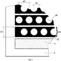
Fig. 2 zeigt schematisch einen Ausschnitt eines Dünnschichtsolarmodules 10, bei dem aus den Flächen der nicht transparenten Schichten 15 und 16der Solarzellenstreifen 20 Rechtecke so entfernt werden, dass photovoltaisch aktive Restflächen 21 der Breite bRechteck erhalten bleiben, deren Länge bStreifen sich überden ganzen Solarzellenstreifen 20 erstreckt.Die photovoltaischen Restflächen 21 stoßen im Bereich der Srukturierungsschnitte benachbarter Solarzellenstreifen 20 über die Breite bRechteck zusammen. -
Fig. 3 : Aus den nicht transparenten Flächen 21der Solarzellenstreifen 20 des Dünnschichtsolarmodules 10sind Kreise 22 mit festem Abstand aKreise und definiertem Durchmesser dKreise entlang der Mittellinie des Solarzellenstreifens 20 entfernt, wobei gilt: dKreise < bstreifen . Die Mittelpunkte der Kreise 22benachbarter Solarzellenstreifen 20 sind jeweils um den halben Abstand aversatz des Mittelpunktabstandes aKreise zweier Kreise 22eines Solarzellenstreifens 20 gegeneinander versetzt. -
Fig. 4 zeigt schematisch eine Ausführungsform mit einer Vielzahl kreisförmiger transparenter Flächenbereiche 22, die stochastisch indem Solarzellenstreifen 20 verteilt sind. Bei dieser Ausführungsform sind die Abmessungen der kreisförmigen transparenten Flächenbereiche 22 sehr viel kleiner, als die Breite bStreifen der Solarzellenstreifen. -
Fig. 5 zeigt die Realisierung einer "Rechtecktransparenz" von ca. 30% auf der Basis des Dünnschichtmodules 10 des deutschen Geschmacksmusters DM 073 637. -
Fig. 6 zeigt die Realisierung einer "Kreistransparenz" von ca. 30% auf der Basis des Dünnschichtmodules des deutschen Geschmacksmusters DM 073 637. Diese Ausführungsform unterscheidet sich von der inFig. 4 gezeigten durch eine regelmäßige Anordnung der der kreisförmigen transparenten Flächenbereiche in den Solarzellenstreifen.
-
Fig. 1 schematically shows the principle according to the invention of realizing the partial transparency of a thin-filmsolar module 10 in cross section. Thesolar cell 11 consists of the layer stack of the layers- transparent
front contact 14, - non-transparent CdS /
CdTe layer 15 and - has non-transparent
back contact layer 16.
The solar cell is deposited on thefront glass 17. The desired partial transparency results from the removal of definedtransparent areas 19 of thenon-transparent layers non-transparent layers solar module 10 in such a way that the transparentfront contact layer 14 is retained (avoidance of additional series resistance). Therear glass 18 is then laminated on as in the normal manufacture of the thin-filmsolar module 10. - transparent
-
Fig. 2 schematically shows a section of a thin-filmsolar module 10, in which rectangles are removed from the areas of thenon-transparent layers solar cell strips 20 in such a way that photovoltaically activeresidual areas 21 of width b rectangle are retained, the length b strips of which extend over the entiresolar cell strip 20 extends. The photovoltaicresidual areas 21 collide in the area of the structuring cuts of adjacent solar cell strips 20 over the width b rectangle . -
Fig. 3 :Circles 22 with a fixed spacing a circles and a defined diameter d circles along the center line of thesolar cell strip 20 are removed from thenon-transparent areas 21 of the solar cell strips 20 of the thin-filmsolar module 10, where the following applies: d circles <strips. The center points of thecircles 22 of adjacent solar cell strips 20 are offset from one another by half the distance apart from the center point distance a circles of twocircles 22 of asolar cell strip 20. -
Fig. 4 schematically shows an embodiment with a plurality of circulartransparent surface areas 22, which are distributed stochastically in thesolar cell strip 20. In this embodiment, the dimensions of the circulartransparent surface areas 22 are very much smaller than the width b strips of the solar cell strips . -
Fig. 5 shows the realization of a "rectangle transparency" of approx. 30% on the basis of the thin-film module 10 of the German design DM 073 637. -
Fig. 6 shows the realization of a "circular transparency" of approx. 30% on the basis of the thin-film module of the German design DM 073 637. This Embodiment differs from that in FIGFig. 4 shown by a regular arrangement of the circular transparent surface areas in the solar cell strips.
- 11
- einfallendes Lichtincident light
- 22nd
- durch die frei definierbaren Flächenbereiche hindurchtretendes Lichtlight passing through the freely definable surface areas
- 33rd
- entschichteter Rand des Solarzellenmodulsstripped edge of the solar cell module
- 44th
- Solarzellenstreifen mit KontaktbusSolar cell strips with contact bus
- 1010th
- DünnschichtsolarzellenmodulThin-film solar cell module
- 1111
- SolarzelleSolar cell
- 1414
- FrontkontaktschichtFront contact layer
- 1515
- nicht transparenter CdS/CdTe-Schichtnon-transparent CdS / CdTe layer
- 1616
- nicht transparenter Rückkontaktschichtnon-transparent back contact layer
- 1717th
- FrontglasFront glass
- 1818th
- RückglasBack glass
- 1919th
- transparenter Bereich mit entfernter Schichtstruktur (Flächenbereich)transparent area with removed layer structure (surface area)
- 2020th
- SolarzellenstreifenSolar cell strips
- 2121
- nicht transparente Flächen (photovoltaisch aktive Bereiche)non-transparent surfaces (photovoltaically active areas)
- 2222
- kreisförmige Flächenbereiche (Kreise)circular surface areas (circles)
- bRbR
- Breite bRechteck der rechteckigen aktiven RestflächenWidth b rectangle of the rectangular active remaining areas
- bSbS
- Länge bstreifen der rechteckigen aktiven RestflächenLength of the rectangular active residual areas
- aKaK
- Abstand aKreise der kreisförmigen Flächenbereiche (Kreise)Distance a circles of the circular surface areas (circles)
- dKdK
- Durchmesser dKreise der kreisförmigen Flächenbereiche (Kreise)Diameter d circles of the circular surface areas (circles)
- vKvK
- Abstand aVersatz der Mittelpunkte der kreisförmigen Flächenbereiche (Kreise) in benachbarten StreifenDistance a Offset of the center points of the circular surface areas (circles) in adjacent strips
Claims (6)
- A method for the manufacture of a partially transparent thin-layer solar module (10) in a substrate configuration, comprising at least the following steps:- providing a substrate (18)- applying a transparent or opaque back contact layer (16)- applying a photovoltaically active semiconductor layer (15) which is opaque or only very slightly transparent- applying a transparent front contact layer (14)- structuring the layers by means of parallel structuring strips and dividing the coating into individual solar cell strips (20) which are connected in series,characterized in that- defined surface regions (19, 22) are removed from the back contact layer (16) and the semiconductor layer (15) prior to depositing the front contact layer (14)- the removed surface regions (19, 22) are filled in with a transparent or coloured transparent plastic and then the transparent front contact layer (14) is deposited over the transparent and opaque surface regions (19, 22; 21).
- The method as claimed in claim 1, characterized in that the transparent surface regions (19, 22) are disposed on the module surface in a random or regular manner.
- The method as claimed in one of the preceding claims, characterized in that the transparent surface regions (19, 22) preferably:- are disposed symmetrically along the solar cell strips (20),- do not exceed the width of the solar cell strip (20),- have the same total area of the transparent surface regions (19, 22) for all of the solar cell strips (20).
- The method as claimed in one of the preceding claims, characterized in that the defined surface regions (19, 22) with the removed semiconductor layer (15) and back contact layer (16) are produced by widening the structuring lines to any extent to produce the desired partial transparency.
- The method as claimed in one of the preceding claims, characterized in that the defined surface regions (19, 22) with the removed semiconductor layer (15) and back contact layer (16) are in the region of the solar cell strips (20) and have the following shape:- rectangular- parallelogram- circular- triangular- trapezoidal- polygonal.
- The method as claimed in one of the preceding claims, characterized in that the defined surface regions (19, 22) in the semiconductor layer (15) and back contact layer (16) are removed by means of a:- laser process,- mechanical scoring process,- lift-off process,- etching process,- sandblasting process.
Applications Claiming Priority (2)
| Application Number | Priority Date | Filing Date | Title |
|---|---|---|---|
| CN201310613095.XA CN104425637A (en) | 2013-08-30 | 2013-08-30 | Partially transparent thin solar module |
| PCT/EP2014/068192 WO2015028519A1 (en) | 2013-08-30 | 2014-08-27 | Partly-transparent thin-film solar module |
Publications (2)
| Publication Number | Publication Date |
|---|---|
| EP3039718A1 EP3039718A1 (en) | 2016-07-06 |
| EP3039718B1 true EP3039718B1 (en) | 2020-04-22 |
Family
ID=51627258
Family Applications (1)
| Application Number | Title | Priority Date | Filing Date |
|---|---|---|---|
| EP14777014.3A Active EP3039718B1 (en) | 2013-08-30 | 2014-08-27 | Partly-transparent thin-film solar module |
Country Status (5)
| Country | Link |
|---|---|
| US (1) | US20160276510A1 (en) |
| EP (1) | EP3039718B1 (en) |
| CN (1) | CN104425637A (en) |
| ES (1) | ES2804303T3 (en) |
| WO (1) | WO2015028519A1 (en) |
Families Citing this family (3)
| Publication number | Priority date | Publication date | Assignee | Title |
|---|---|---|---|---|
| FR3045945B1 (en) * | 2015-12-16 | 2017-12-15 | Sunpartner Technologies | OPTICAL DEVICE FOR DECREASING THE VISIBILITY OF ELECTRICAL INTERCONNECTIONS IN THIN-FILM SEMI-TRANSPARENT PHOTOVOLTAIC MODULES |
| WO2018119680A1 (en) * | 2016-12-27 | 2018-07-05 | China Triumph International Engineering Co., Ltd. | Method and system for monitoring laser scribing process for forming isolation trenches in solar module |
| DE202022000302U1 (en) | 2022-02-05 | 2022-02-22 | Rudi Danz | Semi-transparent solar modules and their applications |
Citations (1)
| Publication number | Priority date | Publication date | Assignee | Title |
|---|---|---|---|---|
| US20110017280A1 (en) * | 2008-02-07 | 2011-01-27 | Philip Thomas Rumsby | Partially transparent solar panel |
Family Cites Families (17)
| Publication number | Priority date | Publication date | Assignee | Title |
|---|---|---|---|---|
| US4795500A (en) * | 1985-07-02 | 1989-01-03 | Sanyo Electric Co., Ltd. | Photovoltaic device |
| DE3712589A1 (en) | 1987-04-14 | 1988-11-03 | Nukem Gmbh | METHOD FOR THE PRODUCTION OF SERIES LAYERED SOLAR CELLS |
| GB2260220B (en) * | 1991-09-10 | 1996-01-03 | Sanyo Electric Co | An amorphous silicon solar cell and method of the solar cell manufacture |
| DE4324318C1 (en) | 1993-07-20 | 1995-01-12 | Siemens Ag | Method for series connection of an integrated thin-film solar cell arrangement |
| JP2000223727A (en) * | 1999-01-28 | 2000-08-11 | Fuji Electric Co Ltd | Thin film solar battery and its manufacture |
| JP2003305577A (en) * | 2002-04-11 | 2003-10-28 | Sharp Corp | Laser beam machining device, manufacturing method of semiconductor element using the same, and manufacturing method of solar battery element using the same |
| KR20050094406A (en) * | 2003-01-10 | 2005-09-27 | 가부시키가이샤 가네카 | Transparent thin-film solar cell module and its manufacturing method |
| JP4448371B2 (en) * | 2004-04-19 | 2010-04-07 | シャープ株式会社 | Light source integrated solar cell module and power generation light emitting unit using the same |
| DE102004057663B4 (en) * | 2004-09-15 | 2015-08-20 | Sunways Ag | Solar module with regularly arranged holes semitransparent crystalline solar cells and method of preparation |
| GB2446838A (en) * | 2007-02-20 | 2008-08-27 | David John Ruchat | Photovoltaic device and manufacturing method |
| TWI379425B (en) * | 2007-12-13 | 2012-12-11 | Nexpower Technology Corp | Translucent solar cell and manufacturing method thereof |
| KR101161378B1 (en) * | 2008-09-09 | 2012-07-02 | 엘지전자 주식회사 | Thin-film type solar cell having white reflective media layer and fabricating method thereof |
| DE102009022378B4 (en) * | 2009-05-23 | 2013-02-07 | Solarion Ag Photovoltaik | Process for the preparation of semi-transparent flexible thin-film solar cells and semi-transparent flexible thin-film solar cell |
| CN101958361A (en) * | 2009-07-13 | 2011-01-26 | 无锡尚德太阳能电力有限公司 | Method for etching transparent thin-film solar cell component |
| GB2472608B (en) * | 2009-08-12 | 2013-09-04 | M Solv Ltd | Method and Apparatus for making a solar panel that is partially transparent |
| JP5325139B2 (en) * | 2010-02-19 | 2013-10-23 | 東レエンジニアリング株式会社 | Solar cell module |
| TW201248876A (en) * | 2011-05-17 | 2012-12-01 | Axuntek Solar Energy | See-through solar battery module and manufacturing method thereof |
-
2013
- 2013-08-30 CN CN201310613095.XA patent/CN104425637A/en active Pending
-
2014
- 2014-08-27 EP EP14777014.3A patent/EP3039718B1/en active Active
- 2014-08-27 US US14/915,104 patent/US20160276510A1/en not_active Abandoned
- 2014-08-27 WO PCT/EP2014/068192 patent/WO2015028519A1/en active Application Filing
- 2014-08-27 ES ES14777014T patent/ES2804303T3/en active Active
Patent Citations (1)
| Publication number | Priority date | Publication date | Assignee | Title |
|---|---|---|---|---|
| US20110017280A1 (en) * | 2008-02-07 | 2011-01-27 | Philip Thomas Rumsby | Partially transparent solar panel |
Also Published As
| Publication number | Publication date |
|---|---|
| US20160276510A1 (en) | 2016-09-22 |
| ES2804303T3 (en) | 2021-02-05 |
| CN104425637A (en) | 2015-03-18 |
| EP3039718A1 (en) | 2016-07-06 |
| WO2015028519A1 (en) | 2015-03-05 |
Similar Documents
| Publication | Publication Date | Title |
|---|---|---|
| DE60222004T2 (en) | TRANSPARENT SUBSTRATE COATED WITH AN ELECTRODE | |
| DE69730337T2 (en) | PHOTOVOLTAIC FILM AND METHOD FOR THE PRODUCTION THEREOF | |
| DE10017610C2 (en) | Process for producing a solar module with integrated series-connected thin-film solar cells and use thereof | |
| EP2537065B1 (en) | Electrochromic glazing with cells connected in series and method for producing same | |
| EP2179426B1 (en) | Multilayer system comprising contact elements, and method for the production of a contact element for a multilayer system | |
| DE102017203105B4 (en) | Glazing unit, process for their preparation and their use | |
| DE102009041941A1 (en) | Thin-film type solar cell and method for producing the same | |
| EP2758993B1 (en) | Thin film solar module having series connection and method for the series connection of thin film solar cells | |
| DE19713215A1 (en) | Solar cell with textured transparent conductive oxide layer | |
| DE102013220802A1 (en) | Solar module and method for producing a solar module | |
| DE102014200956A1 (en) | Photovoltaic cell, photovoltaic module and its manufacture and use | |
| EP1638150A2 (en) | Solar module | |
| EP3039718B1 (en) | Partly-transparent thin-film solar module | |
| DE112009001438B4 (en) | Photoelectric thin-film converter and method for its production | |
| DE102011010131A1 (en) | Raw module for the production of a thin-film solar module and thin-film solar module | |
| DE102008050332A1 (en) | Photovoltaic cell comprises a photovoltaic conversion layer, a lower electrode layer applied on a lower surface of the photovoltaic conversion layer, and a multilayer foil applied on an upper surface of the photovoltaic conversion layer | |
| DE4201571C2 (en) | Method for producing a solar cell that is partially transparent to light and a corresponding solar module | |
| DE102016125637A1 (en) | Photovoltaic module and method for producing a photovoltaic module | |
| DE202021003960U1 (en) | A thin film solar cell | |
| DE202010013136U1 (en) | Thin-film photovoltaic module | |
| AT512678B1 (en) | Photovoltaic window and / or façade element | |
| DE102010017246A1 (en) | Solar cell module and manufacturing method therefor | |
| DE102014216792A1 (en) | Method for producing a transparent electrode of an optoelectronic component | |
| EP2590230A2 (en) | Open air photovoltaic assembly | |
| WO2013045147A1 (en) | Semitransparent solar module and glazing element |
Legal Events
| Date | Code | Title | Description |
|---|---|---|---|
| PUAI | Public reference made under article 153(3) epc to a published international application that has entered the european phase |
Free format text: ORIGINAL CODE: 0009012 |
|
| 17P | Request for examination filed |
Effective date: 20160226 |
|
| AK | Designated contracting states |
Kind code of ref document: A1 Designated state(s): AL AT BE BG CH CY CZ DE DK EE ES FI FR GB GR HR HU IE IS IT LI LT LU LV MC MK MT NL NO PL PT RO RS SE SI SK SM TR |
|
| AX | Request for extension of the european patent |
Extension state: BA ME |
|
| DAX | Request for extension of the european patent (deleted) | ||
| STAA | Information on the status of an ep patent application or granted ep patent |
Free format text: STATUS: EXAMINATION IS IN PROGRESS |
|
| 17Q | First examination report despatched |
Effective date: 20181106 |
|
| GRAP | Despatch of communication of intention to grant a patent |
Free format text: ORIGINAL CODE: EPIDOSNIGR1 |
|
| STAA | Information on the status of an ep patent application or granted ep patent |
Free format text: STATUS: GRANT OF PATENT IS INTENDED |
|
| INTG | Intention to grant announced |
Effective date: 20191119 |
|
| GRAS | Grant fee paid |
Free format text: ORIGINAL CODE: EPIDOSNIGR3 |
|
| GRAA | (expected) grant |
Free format text: ORIGINAL CODE: 0009210 |
|
| STAA | Information on the status of an ep patent application or granted ep patent |
Free format text: STATUS: THE PATENT HAS BEEN GRANTED |
|
| AK | Designated contracting states |
Kind code of ref document: B1 Designated state(s): AL AT BE BG CH CY CZ DE DK EE ES FI FR GB GR HR HU IE IS IT LI LT LU LV MC MK MT NL NO PL PT RO RS SE SI SK SM TR |
|
| REG | Reference to a national code |
Ref country code: CH Ref legal event code: EP |
|
| REG | Reference to a national code |
Ref country code: IE Ref legal event code: FG4D Free format text: LANGUAGE OF EP DOCUMENT: GERMAN |
|
| REG | Reference to a national code |
Ref country code: DE Ref legal event code: R096 Ref document number: 502014014048 Country of ref document: DE |
|
| REG | Reference to a national code |
Ref country code: AT Ref legal event code: REF Ref document number: 1261273 Country of ref document: AT Kind code of ref document: T Effective date: 20200515 |
|
| RAP2 | Party data changed (patent owner data changed or rights of a patent transferred) |
Owner name: CTF SOLAR GMBH Owner name: CHINA TRIUMPH INTERNATIONAL ENGINEERING CO., LTD. |
|
| REG | Reference to a national code |
Ref country code: NL Ref legal event code: FP |
|
| REG | Reference to a national code |
Ref country code: LT Ref legal event code: MG4D |
|
| RAP2 | Party data changed (patent owner data changed or rights of a patent transferred) |
Owner name: CTF SOLAR GMBH Owner name: CHINA TRIUMPH INTERNATIONAL ENGINEERING CO., LTD. |
|
| PG25 | Lapsed in a contracting state [announced via postgrant information from national office to epo] |
Ref country code: LT Free format text: LAPSE BECAUSE OF FAILURE TO SUBMIT A TRANSLATION OF THE DESCRIPTION OR TO PAY THE FEE WITHIN THE PRESCRIBED TIME-LIMIT Effective date: 20200422 Ref country code: NO Free format text: LAPSE BECAUSE OF FAILURE TO SUBMIT A TRANSLATION OF THE DESCRIPTION OR TO PAY THE FEE WITHIN THE PRESCRIBED TIME-LIMIT Effective date: 20200722 Ref country code: GR Free format text: LAPSE BECAUSE OF FAILURE TO SUBMIT A TRANSLATION OF THE DESCRIPTION OR TO PAY THE FEE WITHIN THE PRESCRIBED TIME-LIMIT Effective date: 20200723 Ref country code: PT Free format text: LAPSE BECAUSE OF FAILURE TO SUBMIT A TRANSLATION OF THE DESCRIPTION OR TO PAY THE FEE WITHIN THE PRESCRIBED TIME-LIMIT Effective date: 20200824 Ref country code: FI Free format text: LAPSE BECAUSE OF FAILURE TO SUBMIT A TRANSLATION OF THE DESCRIPTION OR TO PAY THE FEE WITHIN THE PRESCRIBED TIME-LIMIT Effective date: 20200422 Ref country code: IS Free format text: LAPSE BECAUSE OF FAILURE TO SUBMIT A TRANSLATION OF THE DESCRIPTION OR TO PAY THE FEE WITHIN THE PRESCRIBED TIME-LIMIT Effective date: 20200822 Ref country code: SE Free format text: LAPSE BECAUSE OF FAILURE TO SUBMIT A TRANSLATION OF THE DESCRIPTION OR TO PAY THE FEE WITHIN THE PRESCRIBED TIME-LIMIT Effective date: 20200422 |
|
| PG25 | Lapsed in a contracting state [announced via postgrant information from national office to epo] |
Ref country code: HR Free format text: LAPSE BECAUSE OF FAILURE TO SUBMIT A TRANSLATION OF THE DESCRIPTION OR TO PAY THE FEE WITHIN THE PRESCRIBED TIME-LIMIT Effective date: 20200422 Ref country code: RS Free format text: LAPSE BECAUSE OF FAILURE TO SUBMIT A TRANSLATION OF THE DESCRIPTION OR TO PAY THE FEE WITHIN THE PRESCRIBED TIME-LIMIT Effective date: 20200422 Ref country code: LV Free format text: LAPSE BECAUSE OF FAILURE TO SUBMIT A TRANSLATION OF THE DESCRIPTION OR TO PAY THE FEE WITHIN THE PRESCRIBED TIME-LIMIT Effective date: 20200422 Ref country code: BG Free format text: LAPSE BECAUSE OF FAILURE TO SUBMIT A TRANSLATION OF THE DESCRIPTION OR TO PAY THE FEE WITHIN THE PRESCRIBED TIME-LIMIT Effective date: 20200722 |
|
| PG25 | Lapsed in a contracting state [announced via postgrant information from national office to epo] |
Ref country code: AL Free format text: LAPSE BECAUSE OF FAILURE TO SUBMIT A TRANSLATION OF THE DESCRIPTION OR TO PAY THE FEE WITHIN THE PRESCRIBED TIME-LIMIT Effective date: 20200422 |
|
| REG | Reference to a national code |
Ref country code: DE Ref legal event code: R097 Ref document number: 502014014048 Country of ref document: DE |
|
| PG25 | Lapsed in a contracting state [announced via postgrant information from national office to epo] |
Ref country code: CZ Free format text: LAPSE BECAUSE OF FAILURE TO SUBMIT A TRANSLATION OF THE DESCRIPTION OR TO PAY THE FEE WITHIN THE PRESCRIBED TIME-LIMIT Effective date: 20200422 Ref country code: RO Free format text: LAPSE BECAUSE OF FAILURE TO SUBMIT A TRANSLATION OF THE DESCRIPTION OR TO PAY THE FEE WITHIN THE PRESCRIBED TIME-LIMIT Effective date: 20200422 Ref country code: DK Free format text: LAPSE BECAUSE OF FAILURE TO SUBMIT A TRANSLATION OF THE DESCRIPTION OR TO PAY THE FEE WITHIN THE PRESCRIBED TIME-LIMIT Effective date: 20200422 Ref country code: EE Free format text: LAPSE BECAUSE OF FAILURE TO SUBMIT A TRANSLATION OF THE DESCRIPTION OR TO PAY THE FEE WITHIN THE PRESCRIBED TIME-LIMIT Effective date: 20200422 Ref country code: SM Free format text: LAPSE BECAUSE OF FAILURE TO SUBMIT A TRANSLATION OF THE DESCRIPTION OR TO PAY THE FEE WITHIN THE PRESCRIBED TIME-LIMIT Effective date: 20200422 |
|
| REG | Reference to a national code |
Ref country code: ES Ref legal event code: FG2A Ref document number: 2804303 Country of ref document: ES Kind code of ref document: T3 Effective date: 20210205 |
|
| PG25 | Lapsed in a contracting state [announced via postgrant information from national office to epo] |
Ref country code: SK Free format text: LAPSE BECAUSE OF FAILURE TO SUBMIT A TRANSLATION OF THE DESCRIPTION OR TO PAY THE FEE WITHIN THE PRESCRIBED TIME-LIMIT Effective date: 20200422 Ref country code: PL Free format text: LAPSE BECAUSE OF FAILURE TO SUBMIT A TRANSLATION OF THE DESCRIPTION OR TO PAY THE FEE WITHIN THE PRESCRIBED TIME-LIMIT Effective date: 20200422 |
|
| PLBE | No opposition filed within time limit |
Free format text: ORIGINAL CODE: 0009261 |
|
| STAA | Information on the status of an ep patent application or granted ep patent |
Free format text: STATUS: NO OPPOSITION FILED WITHIN TIME LIMIT |
|
| 26N | No opposition filed |
Effective date: 20210125 |
|
| PG25 | Lapsed in a contracting state [announced via postgrant information from national office to epo] |
Ref country code: MC Free format text: LAPSE BECAUSE OF FAILURE TO SUBMIT A TRANSLATION OF THE DESCRIPTION OR TO PAY THE FEE WITHIN THE PRESCRIBED TIME-LIMIT Effective date: 20200422 |
|
| REG | Reference to a national code |
Ref country code: CH Ref legal event code: PL |
|
| PG25 | Lapsed in a contracting state [announced via postgrant information from national office to epo] |
Ref country code: LU Free format text: LAPSE BECAUSE OF NON-PAYMENT OF DUE FEES Effective date: 20200827 Ref country code: LI Free format text: LAPSE BECAUSE OF NON-PAYMENT OF DUE FEES Effective date: 20200831 Ref country code: CH Free format text: LAPSE BECAUSE OF NON-PAYMENT OF DUE FEES Effective date: 20200831 |
|
| REG | Reference to a national code |
Ref country code: BE Ref legal event code: MM Effective date: 20200831 |
|
| PG25 | Lapsed in a contracting state [announced via postgrant information from national office to epo] |
Ref country code: SI Free format text: LAPSE BECAUSE OF FAILURE TO SUBMIT A TRANSLATION OF THE DESCRIPTION OR TO PAY THE FEE WITHIN THE PRESCRIBED TIME-LIMIT Effective date: 20200422 |
|
| PG25 | Lapsed in a contracting state [announced via postgrant information from national office to epo] |
Ref country code: BE Free format text: LAPSE BECAUSE OF NON-PAYMENT OF DUE FEES Effective date: 20200831 Ref country code: IE Free format text: LAPSE BECAUSE OF NON-PAYMENT OF DUE FEES Effective date: 20200827 |
|
| REG | Reference to a national code |
Ref country code: AT Ref legal event code: MM01 Ref document number: 1261273 Country of ref document: AT Kind code of ref document: T Effective date: 20200827 |
|
| PG25 | Lapsed in a contracting state [announced via postgrant information from national office to epo] |
Ref country code: AT Free format text: LAPSE BECAUSE OF NON-PAYMENT OF DUE FEES Effective date: 20200827 |
|
| PG25 | Lapsed in a contracting state [announced via postgrant information from national office to epo] |
Ref country code: TR Free format text: LAPSE BECAUSE OF FAILURE TO SUBMIT A TRANSLATION OF THE DESCRIPTION OR TO PAY THE FEE WITHIN THE PRESCRIBED TIME-LIMIT Effective date: 20200422 Ref country code: MT Free format text: LAPSE BECAUSE OF FAILURE TO SUBMIT A TRANSLATION OF THE DESCRIPTION OR TO PAY THE FEE WITHIN THE PRESCRIBED TIME-LIMIT Effective date: 20200422 Ref country code: CY Free format text: LAPSE BECAUSE OF FAILURE TO SUBMIT A TRANSLATION OF THE DESCRIPTION OR TO PAY THE FEE WITHIN THE PRESCRIBED TIME-LIMIT Effective date: 20200422 |
|
| PG25 | Lapsed in a contracting state [announced via postgrant information from national office to epo] |
Ref country code: MK Free format text: LAPSE BECAUSE OF FAILURE TO SUBMIT A TRANSLATION OF THE DESCRIPTION OR TO PAY THE FEE WITHIN THE PRESCRIBED TIME-LIMIT Effective date: 20200422 |
|
| PGFP | Annual fee paid to national office [announced via postgrant information from national office to epo] |
Ref country code: NL Payment date: 20230822 Year of fee payment: 10 |
|
| PGFP | Annual fee paid to national office [announced via postgrant information from national office to epo] |
Ref country code: IT Payment date: 20230823 Year of fee payment: 10 Ref country code: GB Payment date: 20230823 Year of fee payment: 10 Ref country code: ES Payment date: 20230918 Year of fee payment: 10 |
|
| PGFP | Annual fee paid to national office [announced via postgrant information from national office to epo] |
Ref country code: FR Payment date: 20230822 Year of fee payment: 10 Ref country code: DE Payment date: 20230822 Year of fee payment: 10 |