EP3035779A1 - Integrated system of an electronic module and conductive fabric and method of making the same - Google Patents
Integrated system of an electronic module and conductive fabric and method of making the same Download PDFInfo
- Publication number
- EP3035779A1 EP3035779A1 EP15201038.5A EP15201038A EP3035779A1 EP 3035779 A1 EP3035779 A1 EP 3035779A1 EP 15201038 A EP15201038 A EP 15201038A EP 3035779 A1 EP3035779 A1 EP 3035779A1
- Authority
- EP
- European Patent Office
- Prior art keywords
- conductive fabric
- module
- conductive
- fastener
- electronics module
- Prior art date
- Legal status (The legal status is an assumption and is not a legal conclusion. Google has not performed a legal analysis and makes no representation as to the accuracy of the status listed.)
- Withdrawn
Links
Images


Classifications
-
- H—ELECTRICITY
- H05—ELECTRIC TECHNIQUES NOT OTHERWISE PROVIDED FOR
- H05K—PRINTED CIRCUITS; CASINGS OR CONSTRUCTIONAL DETAILS OF ELECTRIC APPARATUS; MANUFACTURE OF ASSEMBLAGES OF ELECTRICAL COMPONENTS
- H05K1/00—Printed circuits
- H05K1/02—Details
- H05K1/03—Use of materials for the substrate
- H05K1/038—Textiles
-
- H—ELECTRICITY
- H10—SEMICONDUCTOR DEVICES; ELECTRIC SOLID-STATE DEVICES NOT OTHERWISE PROVIDED FOR
- H10W—GENERIC PACKAGES, INTERCONNECTIONS, CONNECTORS OR OTHER CONSTRUCTIONAL DETAILS OF DEVICES COVERED BY CLASS H10
- H10W90/00—Package configurations
-
- D—TEXTILES; PAPER
- D03—WEAVING
- D03D—WOVEN FABRICS; METHODS OF WEAVING; LOOMS
- D03D1/00—Woven fabrics designed to make specified articles
- D03D1/0088—Fabrics having an electronic function
-
- H—ELECTRICITY
- H05—ELECTRIC TECHNIQUES NOT OTHERWISE PROVIDED FOR
- H05K—PRINTED CIRCUITS; CASINGS OR CONSTRUCTIONAL DETAILS OF ELECTRIC APPARATUS; MANUFACTURE OF ASSEMBLAGES OF ELECTRICAL COMPONENTS
- H05K1/00—Printed circuits
- H05K1/02—Details
- H05K1/09—Use of materials for the conductive, e.g. metallic pattern
-
- H—ELECTRICITY
- H05—ELECTRIC TECHNIQUES NOT OTHERWISE PROVIDED FOR
- H05K—PRINTED CIRCUITS; CASINGS OR CONSTRUCTIONAL DETAILS OF ELECTRIC APPARATUS; MANUFACTURE OF ASSEMBLAGES OF ELECTRICAL COMPONENTS
- H05K1/00—Printed circuits
- H05K1/02—Details
- H05K1/11—Printed elements for providing electric connections to or between printed circuits
- H05K1/115—Via connections; Lands around holes or via connections
-
- H—ELECTRICITY
- H05—ELECTRIC TECHNIQUES NOT OTHERWISE PROVIDED FOR
- H05K—PRINTED CIRCUITS; CASINGS OR CONSTRUCTIONAL DETAILS OF ELECTRIC APPARATUS; MANUFACTURE OF ASSEMBLAGES OF ELECTRICAL COMPONENTS
- H05K1/00—Printed circuits
- H05K1/18—Printed circuits structurally associated with non-printed electric components
- H05K1/181—Printed circuits structurally associated with non-printed electric components associated with surface mounted components
-
- H—ELECTRICITY
- H05—ELECTRIC TECHNIQUES NOT OTHERWISE PROVIDED FOR
- H05K—PRINTED CIRCUITS; CASINGS OR CONSTRUCTIONAL DETAILS OF ELECTRIC APPARATUS; MANUFACTURE OF ASSEMBLAGES OF ELECTRICAL COMPONENTS
- H05K3/00—Apparatus or processes for manufacturing printed circuits
- H05K3/10—Apparatus or processes for manufacturing printed circuits in which conductive material is applied to the insulating support in such a manner as to form the desired conductive pattern
-
- H—ELECTRICITY
- H05—ELECTRIC TECHNIQUES NOT OTHERWISE PROVIDED FOR
- H05K—PRINTED CIRCUITS; CASINGS OR CONSTRUCTIONAL DETAILS OF ELECTRIC APPARATUS; MANUFACTURE OF ASSEMBLAGES OF ELECTRICAL COMPONENTS
- H05K3/00—Apparatus or processes for manufacturing printed circuits
- H05K3/30—Assembling printed circuits with electric components, e.g. with resistors
- H05K3/32—Assembling printed circuits with electric components, e.g. with resistors electrically connecting electric components or wires to printed circuits
-
- H—ELECTRICITY
- H10—SEMICONDUCTOR DEVICES; ELECTRIC SOLID-STATE DEVICES NOT OTHERWISE PROVIDED FOR
- H10W—GENERIC PACKAGES, INTERCONNECTIONS, CONNECTORS OR OTHER CONSTRUCTIONAL DETAILS OF DEVICES COVERED BY CLASS H10
- H10W72/00—Interconnections or connectors in packages
-
- H—ELECTRICITY
- H10—SEMICONDUCTOR DEVICES; ELECTRIC SOLID-STATE DEVICES NOT OTHERWISE PROVIDED FOR
- H10W—GENERIC PACKAGES, INTERCONNECTIONS, CONNECTORS OR OTHER CONSTRUCTIONAL DETAILS OF DEVICES COVERED BY CLASS H10
- H10W95/00—Packaging processes not covered by the other groups of this subclass
-
- H—ELECTRICITY
- H05—ELECTRIC TECHNIQUES NOT OTHERWISE PROVIDED FOR
- H05K—PRINTED CIRCUITS; CASINGS OR CONSTRUCTIONAL DETAILS OF ELECTRIC APPARATUS; MANUFACTURE OF ASSEMBLAGES OF ELECTRICAL COMPONENTS
- H05K1/00—Printed circuits
- H05K1/02—Details
- H05K1/0277—Bendability or stretchability details
- H05K1/0283—Stretchable printed circuits
-
- H—ELECTRICITY
- H05—ELECTRIC TECHNIQUES NOT OTHERWISE PROVIDED FOR
- H05K—PRINTED CIRCUITS; CASINGS OR CONSTRUCTIONAL DETAILS OF ELECTRIC APPARATUS; MANUFACTURE OF ASSEMBLAGES OF ELECTRICAL COMPONENTS
- H05K1/00—Printed circuits
- H05K1/02—Details
- H05K1/03—Use of materials for the substrate
- H05K1/0313—Organic insulating material
- H05K1/0353—Organic insulating material consisting of two or more materials, e.g. two or more polymers, polymer + filler, + reinforcement
- H05K1/0366—Organic insulating material consisting of two or more materials, e.g. two or more polymers, polymer + filler, + reinforcement reinforced, e.g. by fibres, fabrics
-
- H—ELECTRICITY
- H05—ELECTRIC TECHNIQUES NOT OTHERWISE PROVIDED FOR
- H05K—PRINTED CIRCUITS; CASINGS OR CONSTRUCTIONAL DETAILS OF ELECTRIC APPARATUS; MANUFACTURE OF ASSEMBLAGES OF ELECTRICAL COMPONENTS
- H05K1/00—Printed circuits
- H05K1/02—Details
- H05K1/03—Use of materials for the substrate
- H05K1/0313—Organic insulating material
- H05K1/0353—Organic insulating material consisting of two or more materials, e.g. two or more polymers, polymer + filler, + reinforcement
- H05K1/0373—Organic insulating material consisting of two or more materials, e.g. two or more polymers, polymer + filler, + reinforcement containing additives, e.g. fillers
-
- H—ELECTRICITY
- H05—ELECTRIC TECHNIQUES NOT OTHERWISE PROVIDED FOR
- H05K—PRINTED CIRCUITS; CASINGS OR CONSTRUCTIONAL DETAILS OF ELECTRIC APPARATUS; MANUFACTURE OF ASSEMBLAGES OF ELECTRICAL COMPONENTS
- H05K1/00—Printed circuits
- H05K1/02—Details
- H05K1/11—Printed elements for providing electric connections to or between printed circuits
- H05K1/111—Pads for surface mounting, e.g. lay-out
- H05K1/112—Pads for surface mounting, e.g. lay-out directly combined with via connections
- H05K1/113—Via provided in pad; Pad over filled via
-
- H—ELECTRICITY
- H05—ELECTRIC TECHNIQUES NOT OTHERWISE PROVIDED FOR
- H05K—PRINTED CIRCUITS; CASINGS OR CONSTRUCTIONAL DETAILS OF ELECTRIC APPARATUS; MANUFACTURE OF ASSEMBLAGES OF ELECTRICAL COMPONENTS
- H05K2201/00—Indexing scheme relating to printed circuits covered by H05K1/00
- H05K2201/05—Flexible printed circuits [FPCs]
-
- H—ELECTRICITY
- H05—ELECTRIC TECHNIQUES NOT OTHERWISE PROVIDED FOR
- H05K—PRINTED CIRCUITS; CASINGS OR CONSTRUCTIONAL DETAILS OF ELECTRIC APPARATUS; MANUFACTURE OF ASSEMBLAGES OF ELECTRICAL COMPONENTS
- H05K2201/00—Indexing scheme relating to printed circuits covered by H05K1/00
- H05K2201/09—Shape and layout
- H05K2201/09209—Shape and layout details of conductors
- H05K2201/095—Conductive through-holes or vias
- H05K2201/0959—Plated through-holes or plated blind vias filled with insulating material
-
- H—ELECTRICITY
- H05—ELECTRIC TECHNIQUES NOT OTHERWISE PROVIDED FOR
- H05K—PRINTED CIRCUITS; CASINGS OR CONSTRUCTIONAL DETAILS OF ELECTRIC APPARATUS; MANUFACTURE OF ASSEMBLAGES OF ELECTRICAL COMPONENTS
- H05K2201/00—Indexing scheme relating to printed circuits covered by H05K1/00
- H05K2201/10—Details of components or other objects attached to or integrated in a printed circuit board
- H05K2201/10227—Other objects, e.g. metallic pieces
- H05K2201/10242—Metallic cylinders
-
- H—ELECTRICITY
- H05—ELECTRIC TECHNIQUES NOT OTHERWISE PROVIDED FOR
- H05K—PRINTED CIRCUITS; CASINGS OR CONSTRUCTIONAL DETAILS OF ELECTRIC APPARATUS; MANUFACTURE OF ASSEMBLAGES OF ELECTRICAL COMPONENTS
- H05K2201/00—Indexing scheme relating to printed circuits covered by H05K1/00
- H05K2201/10—Details of components or other objects attached to or integrated in a printed circuit board
- H05K2201/10227—Other objects, e.g. metallic pieces
- H05K2201/10295—Metallic connector elements partly mounted in a hole of the PCB
-
- H—ELECTRICITY
- H05—ELECTRIC TECHNIQUES NOT OTHERWISE PROVIDED FOR
- H05K—PRINTED CIRCUITS; CASINGS OR CONSTRUCTIONAL DETAILS OF ELECTRIC APPARATUS; MANUFACTURE OF ASSEMBLAGES OF ELECTRICAL COMPONENTS
- H05K2201/00—Indexing scheme relating to printed circuits covered by H05K1/00
- H05K2201/10—Details of components or other objects attached to or integrated in a printed circuit board
- H05K2201/10227—Other objects, e.g. metallic pieces
- H05K2201/10295—Metallic connector elements partly mounted in a hole of the PCB
- H05K2201/10303—Pin-in-hole mounted pins
-
- H—ELECTRICITY
- H05—ELECTRIC TECHNIQUES NOT OTHERWISE PROVIDED FOR
- H05K—PRINTED CIRCUITS; CASINGS OR CONSTRUCTIONAL DETAILS OF ELECTRIC APPARATUS; MANUFACTURE OF ASSEMBLAGES OF ELECTRICAL COMPONENTS
- H05K3/00—Apparatus or processes for manufacturing printed circuits
- H05K3/40—Forming printed elements for providing electric connections to or between printed circuits
- H05K3/42—Plated through-holes or plated via connections
-
- H—ELECTRICITY
- H05—ELECTRIC TECHNIQUES NOT OTHERWISE PROVIDED FOR
- H05K—PRINTED CIRCUITS; CASINGS OR CONSTRUCTIONAL DETAILS OF ELECTRIC APPARATUS; MANUFACTURE OF ASSEMBLAGES OF ELECTRICAL COMPONENTS
- H05K9/00—Screening of apparatus or components against electric or magnetic fields
- H05K9/0073—Shielding materials
- H05K9/0081—Electromagnetic shielding materials, e.g. EMI, RFI shielding
- H05K9/009—Electromagnetic shielding materials, e.g. EMI, RFI shielding comprising electro-conductive fibres, e.g. metal fibres, carbon fibres, metallised textile fibres, electro-conductive mesh, woven, non-woven mat, fleece, cross-linked
Definitions
- Embodiments of the present disclosure generally relate to an electronic module assembled to a conductive fabric, and a method of assembling an electronic module to a conductive fabric.
- an assembly of an electronic module on a conductive fabric may be desirable to form an integrated system.
- Conventional assemblies include modules stitched to a conductive fabric using conductive wire. Stitching is an intensive manual process not suitable for high volume or automation. In some stitched assemblies, the stitches become loose as the fabric flexes. It has also been noted that some conductive fabrics are not well suited for joining techniques requiring elevated temperatures.
- an electronic module assembly comprises a non-conductive fabric and a conductive fabric covering at least part of a first side of the non-conductive fabric.
- An electronics module is disposed on the conductive fabric, and a portion of the electronics module includes a wall defining a through hole. A fastener passing through the through hole and passing through the conductive fabric is configured to electronically couple the electronics module to the conductive fabric.
- a method of making an electronics assembly comprising an electronics module and a conductive fabric.
- the method comprises forming a substrate including a conductive fabric covering at least part of a first side of a non-conductive fabric; disposing an electronics module having one or more through holes on the substrate with the through holes aligned with a portion of the conductive fabric; inserting a fastener to pass through the through hole and through the substrate; and clamping the module to the substrate to form an electrical connection using the fastener.
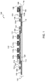
- Figure 1 depicts a side sectional view of an electronics module assembly 100 comprising a substrate 102 including a non-conductive fabric 104, a conductive fabric 110, and an electronics module 116 (one electronics module and a partial are shown in Fog. 1).
- the non-conductive fabric 104 has a first side 106 and a second side 108 opposite and generally parallel with the first side 106.
- the conductive fabric 110 covers at least a part of the first side 106 and may be attached to the non-conductive fabric 104 using one or more of stitching or gluing.
- the thread used to attach the conductive fabric 110 to the non-conductive fabric 104 is preferably a non-conductive thread 112, for example a thread formed from, in non-limiting examples, natural fibers such as cotton, or synthetic fibers such as polyester or nylon. If gluing is used, the glue 114, or adhesive, is preferably non-conductive.
- An electronics module 116 is positioned on the substrate 102 so that a portion of the module 116 is disposed on the conductive fabric 110 with a bottom surface 126 of the module 116 adjacent to the conductive fabric 110 and a top surface 128 spaced apart from the conductive fabric 110.
- the portion 118 disposed on the conductive fabric 110 includes an interior wall 120 that defines a through hole 122 formed through the portion 118.
- the wall 120 is plated with a conductive material 124 which may include, in non-limiting examples, silver, gold over nickel, or tin.
- the bottom surface 126 and the top surface 128 at least partially surrounding the through hole 122 is preferably includes conductive elements 130a, 130b, for example copper pads which may be plated with silver, gold, or nickel.
- the electronics module 116 may include, in non-limiting examples, sensors 116a, light sources such as light emitting diodes (LEDs) 116b, recording devices 116c, displays 116d, and the like. Other electronic devices can be included in the electronics module 116 within the scope and spirit of this disclosure.
- a fastener 202 is used to clamp the electronics module 116 to the substrate 102 to form an electrical connection between the module and the substrate.
- a stem 204 of fastener 202 passes through the through hole 122, penetrates and passes through the conductive fabric 110 and the non-conductive fabric 104 and exits through the second side 108 of the non-conductive fabric 104.
- the conductive and non-conductive fabrics 110, 104 may have preformed holes to allow passage of the fastener 202.
- the fastener 202 may pierce one or both of the conductive and non-conductive fabrics 110, 104, forming an opening therein.
- a first end of the fastener 202 has a head 206 larger than the through hole 122 formed in the electronics module 116.
- the head 206 is configured to contact the conductive elements 130a formed on the top surface 128 of the electronics module 116.
- the second end of the fastener 202 is adapted to accept a mating element 208 to facilitate the clamping.
- the second end of the fastener 202 may include an external thread and the mating element 208 may have a corresponding internal thread to engage the external thread and advance along the length of the stem 204 when rotated.
- the second end of the fastener 202 may be subjected to a compressive load to facilitate clamping. During application of the compressive load, the second end of the fastener 202 may be deformed by the pressure and expand so that the second end becomes larger than the through hole 122.
- the fastener 202 is a conductive element formed from an electrically conductive material, for example metal, or from a non-conductive material that is plated with a conductive material.
- the fastener 202 forms an electrical connection between the electronics module 116 and the conductive fabric 110.
- the fastener 202 forms a gas-tight connection between the electronics module 116 and the conductive fabric 110.
- the disclosed electronics module assembly 100 may provide a durable electrical connection between an electronics module 116, which may be flexible or rigid, and a flexible substrate 102 formed from a conductive fabric 110 and a non-conductive fabric 104.
- the disclosed assembly may be well-suited for manual or automated assembly, for example using the method 300 of Fig. 3 .
- a substrate 102 is formed from a conductive fabric 110 covering at least part of a first side of a non-conductive fabric 104.
- the conductive fabric 110 may be attached to the non-conductive fabric using one or more of stitching or gluing. The attachment may be accomplished using non-conductive thread for stitching or a non-conductive glue or adhesive for gluing.
- an electronics module 116 is disposed on the substrate 102.
- the module 116 includes one or more through holes 122 formed though a portion of the module 116.
- the through hole 122 is placed upon, or aligned with, a portion of the conductive fabric 110.
- a fastener is inserted to pass through the through hole 122 in the electronics module 116 and to pass through the substrate 102.
- One or both of the conductive fabric 110 and the non-conductive fabric 104 may have a preformed hole formed therein to accept the fastener 202.
- the electronics module 116 is clamped to the substrate 102 to form an electrical connection using the fastener 202.
- the inventive module may advantageously provide a durable electrical connection between an electronics module and a substrate.
- the inventive method may facilitate manual or automated assembly of an electronics module to a substrate with increased reliability, thereby improving production throughput.
Landscapes
- Engineering & Computer Science (AREA)
- Microelectronics & Electronic Packaging (AREA)
- Textile Engineering (AREA)
- Manufacturing & Machinery (AREA)
- Printing Elements For Providing Electric Connections Between Printed Circuits (AREA)
- Combinations Of Printed Boards (AREA)
- Electric Connection Of Electric Components To Printed Circuits (AREA)
Abstract
Description
- Embodiments of the present disclosure generally relate to an electronic module assembled to a conductive fabric, and a method of assembling an electronic module to a conductive fabric.
- In some applications, it may be desirable to form an assembly of an electronic module on a conductive fabric to form an integrated system. Conventional assemblies include modules stitched to a conductive fabric using conductive wire. Stitching is an intensive manual process not suitable for high volume or automation. In some stitched assemblies, the stitches become loose as the fabric flexes. It has also been noted that some conductive fabrics are not well suited for joining techniques requiring elevated temperatures.
- Accordingly, a need exists for an improved electronic module assembly and method of assembling an electronic module to a conductive fabric.
- Embodiments of an electronic module assembly and method of assembling an electronic module to a conductive fabric are provided herein. In an embodiment, an electronic module assembly comprises a non-conductive fabric and a conductive fabric covering at least part of a first side of the non-conductive fabric. An electronics module is disposed on the conductive fabric, and a portion of the electronics module includes a wall defining a through hole. A fastener passing through the through hole and passing through the conductive fabric is configured to electronically couple the electronics module to the conductive fabric.
- In an embodiment, a method of making an electronics assembly comprising an electronics module and a conductive fabric is disclosed. The method comprises forming a substrate including a conductive fabric covering at least part of a first side of a non-conductive fabric; disposing an electronics module having one or more through holes on the substrate with the through holes aligned with a portion of the conductive fabric; inserting a fastener to pass through the through hole and through the substrate; and clamping the module to the substrate to form an electrical connection using the fastener.
- Other and further embodiments of the present invention are described below.
- Embodiments of the present invention, briefly summarized above and discussed in greater detail below, can be understood by reference to the illustrative embodiments of the invention depicted in the appended drawings. It is to be noted, however, that the appended drawings illustrate only typical embodiments of this invention and are therefore not to be considered limiting of its scope, for the invention may admit to other equally effective embodiments.
-
Figure 1 depicts a side sectional view of an electronics module assembly in accordance with an embodiment of this disclosure. -
Figure 2 is a side sectional view of an electronics module assembly in accordance with an embodiment of this disclosure. -
Figure 3 is a flow diagram in accordance with an embodiment of a method of this disclosure. - Certain terminology is used in the following description for convenience only and is not limiting. "Conductive" is used to mean "electrically conductive" unless the context clearly calls for a different definition. Conversely, "non-conductive" means resistant to electrical conduction, or an electrical insulator. The words "front," "rear," "upper" and "lower" designate directions in the drawings to which reference is made. A reference to a list of items that are cited as "at least one of a, b, or c" (where a, b, and c represent the items being listed) means any single one of the items a, b, or c, or combinations thereof. The terminology includes the words specifically noted above, derivatives thereof and words of similar import.
-
Figure 1 depicts a side sectional view of anelectronics module assembly 100 comprising asubstrate 102 including anon-conductive fabric 104, aconductive fabric 110, and an electronics module 116 (one electronics module and a partial are shown in Fog. 1). Thenon-conductive fabric 104 has afirst side 106 and asecond side 108 opposite and generally parallel with thefirst side 106. Theconductive fabric 110 covers at least a part of thefirst side 106 and may be attached to thenon-conductive fabric 104 using one or more of stitching or gluing. If stitching is used, the thread used to attach theconductive fabric 110 to thenon-conductive fabric 104 is preferably anon-conductive thread 112, for example a thread formed from, in non-limiting examples, natural fibers such as cotton, or synthetic fibers such as polyester or nylon. If gluing is used, theglue 114, or adhesive, is preferably non-conductive. - An
electronics module 116 is positioned on thesubstrate 102 so that a portion of themodule 116 is disposed on theconductive fabric 110 with abottom surface 126 of themodule 116 adjacent to theconductive fabric 110 and atop surface 128 spaced apart from theconductive fabric 110. Theportion 118 disposed on theconductive fabric 110 includes aninterior wall 120 that defines a throughhole 122 formed through theportion 118. In some embodiments, thewall 120 is plated with aconductive material 124 which may include, in non-limiting examples, silver, gold over nickel, or tin. Thebottom surface 126 and thetop surface 128 at least partially surrounding thethrough hole 122 is preferably includesconductive elements - The
electronics module 116 may include, in non-limiting examples,sensors 116a, light sources such as light emitting diodes (LEDs) 116b,recording devices 116c,displays 116d, and the like. Other electronic devices can be included in theelectronics module 116 within the scope and spirit of this disclosure. - As shown in
Fig. 2 , afastener 202 is used to clamp theelectronics module 116 to thesubstrate 102 to form an electrical connection between the module and the substrate. In the non-limiting embodiment ofFig. 2 , astem 204 offastener 202 passes through thethrough hole 122, penetrates and passes through theconductive fabric 110 and thenon-conductive fabric 104 and exits through thesecond side 108 of thenon-conductive fabric 104. In an embodiment, the conductive and non-conductivefabrics fastener 202. In another embodiment, thefastener 202 may pierce one or both of the conductive and non-conductivefabrics - As shown in
Fig. 2 , a first end of thefastener 202 has ahead 206 larger than the throughhole 122 formed in theelectronics module 116. Thehead 206 is configured to contact theconductive elements 130a formed on thetop surface 128 of theelectronics module 116. In an embodiment, the second end of thefastener 202 is adapted to accept amating element 208 to facilitate the clamping. For example, the second end of thefastener 202 may include an external thread and themating element 208 may have a corresponding internal thread to engage the external thread and advance along the length of thestem 204 when rotated. - In another embodiment, the second end of the
fastener 202 may be subjected to a compressive load to facilitate clamping. During application of the compressive load, the second end of thefastener 202 may be deformed by the pressure and expand so that the second end becomes larger than the throughhole 122. - The
fastener 202 is a conductive element formed from an electrically conductive material, for example metal, or from a non-conductive material that is plated with a conductive material. When theelectronics module 116 is clamped to thesubstrate 102, thefastener 202 forms an electrical connection between theelectronics module 116 and theconductive fabric 110. Thefastener 202 forms a gas-tight connection between theelectronics module 116 and theconductive fabric 110. - The inventors have noted that the disclosed
electronics module assembly 100 may provide a durable electrical connection between anelectronics module 116, which may be flexible or rigid, and aflexible substrate 102 formed from aconductive fabric 110 and anon-conductive fabric 104. The disclosed assembly may be well-suited for manual or automated assembly, for example using themethod 300 ofFig. 3 . - At 302, a
substrate 102 is formed from aconductive fabric 110 covering at least part of a first side of anon-conductive fabric 104. Theconductive fabric 110 may be attached to the non-conductive fabric using one or more of stitching or gluing. The attachment may be accomplished using non-conductive thread for stitching or a non-conductive glue or adhesive for gluing. - At 304, an
electronics module 116 is disposed on thesubstrate 102. Themodule 116 includes one or more throughholes 122 formed though a portion of themodule 116. Whenelectronics module 116 is disposed on thesubstrate 102, the throughhole 122 is placed upon, or aligned with, a portion of theconductive fabric 110. - At 306, a fastener is inserted to pass through the through
hole 122 in theelectronics module 116 and to pass through thesubstrate 102. One or both of theconductive fabric 110 and thenon-conductive fabric 104 may have a preformed hole formed therein to accept thefastener 202. - At 208, the
electronics module 116 is clamped to thesubstrate 102 to form an electrical connection using thefastener 202. - Thus an electronics module assembly and method of assembling an electronic module to a conductive fabric are provided herein. The inventive module may advantageously provide a durable electrical connection between an electronics module and a substrate. The inventive method may facilitate manual or automated assembly of an electronics module to a substrate with increased reliability, thereby improving production throughput.
- Having thus described the present invention in detail, it is to be appreciated and will be apparent to those skilled in the art that many physical changes, only a few of which are exemplified in the detailed description of the invention, could be made without altering the inventive concepts and principles embodied therein. It is also to be appreciated that numerous embodiments incorporating only part of the preferred embodiment are possible which do not alter, with respect to those parts, the inventive concepts and principles embodied therein. The present embodiment and optional configurations are therefore to be considered in all respects as exemplary and/or illustrative and not restrictive, the scope of the invention being indicated by the appended claims rather than by the foregoing description, and all alternate embodiments and changes to this embodiment which come within the meaning and range of equivalency of said claims are therefore to be embraced therein.
Claims (10)
- An electronic module assembly comprising:a non-conductive fabric;a conductive fabric covering at least part of a first side of the non-conductive fabric;an electronics module disposed on the conductive fabric, a portion of the electronics module includes a wall defining a through hole; anda fastener passing through the through hole and passing through the conductive fabric,wherein the fastener is configured to electronically couple the electronics module to the conductive fabric.
- The module of claim 1, wherein the wall is plated with a conductive material.
- The module of claim 1 or 2, wherein the portion of the electronics module comprises a top surface and a bottom surface surrounding the through hole, a portion of the top surface and bottom surface is plated with a conductive material.
- The module of any one of claims 1 to 3, wherein the conductive fabric is attached to the non-conductive fabric substrate using one or more of stitching or gluing.
- The module of any one of claims 1 to 4, wherein the fastener is a metal fastener.
- The module of any one of claims 1 to 5, wherein the fastener includes a metal coating.
- The module of any one of claims 1 to 6, wherein the conductive fabric is formed from a metal plated yarn.
- A method of making an electronics assembly comprising an electronics module and a conductive fabric, comprising:forming a substrate including a conductive fabric covering at least part of a first side of a non-conductive fabric;disposing an electronics module having one or more through holes on the substrate with the through holes aligned with a portion of the conductive fabric;inserting a fastener to pass through the through hole and through the substrate; andclamping the module to the substrate to form an electrical connection using the fastener.
- The method of claim 8, wherein forming the substrate includes:attaching the conductive fabric to the non-conductive fabric using one or more of stitching or gluing.
- The method of claim 8 or 9, wherein the clamping forms a gas tight connection between the module and the conductive fabric.
Applications Claiming Priority (1)
| Application Number | Priority Date | Filing Date | Title |
|---|---|---|---|
| US14/574,944 US10201080B2 (en) | 2014-12-18 | 2014-12-18 | Integrated system of an electronic module and conductive fabric and method of making the same |
Publications (1)
| Publication Number | Publication Date |
|---|---|
| EP3035779A1 true EP3035779A1 (en) | 2016-06-22 |
Family
ID=55070721
Family Applications (1)
| Application Number | Title | Priority Date | Filing Date |
|---|---|---|---|
| EP15201038.5A Withdrawn EP3035779A1 (en) | 2014-12-18 | 2015-12-18 | Integrated system of an electronic module and conductive fabric and method of making the same |
Country Status (3)
| Country | Link |
|---|---|
| US (2) | US10201080B2 (en) |
| EP (1) | EP3035779A1 (en) |
| CN (1) | CN105720045A (en) |
Cited By (1)
| Publication number | Priority date | Publication date | Assignee | Title |
|---|---|---|---|---|
| EP3364731A1 (en) * | 2017-02-20 | 2018-08-22 | IMEC vzw | A system including a conductive textile and an electronic circuit unit and a method |
Families Citing this family (2)
| Publication number | Priority date | Publication date | Assignee | Title |
|---|---|---|---|---|
| US9860982B1 (en) * | 2017-02-26 | 2018-01-02 | Xsensor Technology Corporation | Electrical connection of electrical wires to flexible conductive elements |
| WO2018164732A1 (en) * | 2017-03-09 | 2018-09-13 | Google Llc | Interactive object with multiple electronics modules |
Citations (9)
| Publication number | Priority date | Publication date | Assignee | Title |
|---|---|---|---|---|
| US5991922A (en) * | 1996-12-26 | 1999-11-30 | Banks; David L. | Monitored static electricity dissipation garment |
| US20020173175A1 (en) * | 2001-05-15 | 2002-11-21 | International Business Machines Corporation | Interposer member having apertures for relieving stress and increasing contact compliancy |
| EP2107642A2 (en) * | 2008-04-04 | 2009-10-07 | AMPHENOL-TUCHEL ELECTRONICS GmbH | Connection assembly and method for contacting conducting textile semi-manufactures |
| US20100147562A1 (en) * | 2006-07-10 | 2010-06-17 | Chu Andrew W | Fabric Circuits and Method of Manufacturing Fabric Circuits |
| US20110290544A1 (en) * | 1998-05-19 | 2011-12-01 | Ibiden Co., Ltd. | Printed wiring board and manufacturing method of printed wiring board |
| DE102010060222A1 (en) * | 2010-10-28 | 2012-05-03 | Kunert Fashion Gmbh & Co. Kg | Textile product with at least one electrical or electronic component |
| US20140069704A1 (en) * | 2012-09-07 | 2014-03-13 | R&D Circuits, Inc. | Method and structure for forming contact pads on a printed circuit board using zero under cut technology |
| DE202013002601U1 (en) * | 2013-03-18 | 2014-06-23 | Alpha-Fit Gmbh | Connecting device for textile product |
| US20140313743A1 (en) * | 2011-07-28 | 2014-10-23 | Pole Europeen De Plasturgie | Method for Assembling a Microelectronic Chip Device in a Fabric, Chip Device, and Fabric Incorporating a Crimped Chip Device |
Family Cites Families (11)
| Publication number | Priority date | Publication date | Assignee | Title |
|---|---|---|---|---|
| US4967038A (en) * | 1986-12-16 | 1990-10-30 | Sam Techology Inc. | Dry electrode brain wave recording system |
| CA2426110C (en) * | 2000-10-16 | 2010-06-29 | Foster-Miller, Inc. | A method of manufacturing a fabric article to include electronic circuitry and an electrically active textile article |
| US7461444B2 (en) * | 2004-03-29 | 2008-12-09 | Deaett Michael A | Method for constructing antennas from textile fabrics and components |
| US7191803B2 (en) * | 2004-12-13 | 2007-03-20 | Woven Electronics Corporation | Elastic fabric with sinusoidally disposed wires |
| US7308294B2 (en) * | 2005-03-16 | 2007-12-11 | Textronics Inc. | Textile-based electrode system |
| DE102006027213A1 (en) * | 2006-06-12 | 2007-12-13 | Future-Shape Gmbh | Textile layer arrangement, textile layer array and method for producing a textile layer arrangement |
| KR101549414B1 (en) | 2007-03-29 | 2015-09-02 | 코닌클리케 필립스 엔.브이. | Electronic assembly for attachment to a fabric substrate electronic textile and method of manufacturing such an electronic textile |
| JP5417984B2 (en) * | 2009-05-18 | 2014-02-19 | 株式会社デンソー | Electronic equipment |
| TWM372014U (en) * | 2009-05-26 | 2010-01-01 | Fu-Biau Hsu | Lead frame with stitching-assisting structures, electronic device having such laed frame and apparatus having such electronic devicelead frame illuminating textile article |
| JP5854617B2 (en) * | 2010-03-16 | 2016-02-09 | 韓國電子通信研究院Electronics and Telecommunications Research Institute | Woven type electronic element package, method for manufacturing the same, and method for mounting textile type electronic element package |
| US9521751B2 (en) * | 2013-11-20 | 2016-12-13 | Intel Corporation | Weaved electrical components in a substrate package core |
-
2014
- 2014-12-18 US US14/574,944 patent/US10201080B2/en active Active
-
2015
- 2015-12-18 CN CN201510959097.3A patent/CN105720045A/en active Pending
- 2015-12-18 EP EP15201038.5A patent/EP3035779A1/en not_active Withdrawn
-
2018
- 2018-11-27 US US16/201,116 patent/US11051401B2/en not_active Expired - Fee Related
Patent Citations (9)
| Publication number | Priority date | Publication date | Assignee | Title |
|---|---|---|---|---|
| US5991922A (en) * | 1996-12-26 | 1999-11-30 | Banks; David L. | Monitored static electricity dissipation garment |
| US20110290544A1 (en) * | 1998-05-19 | 2011-12-01 | Ibiden Co., Ltd. | Printed wiring board and manufacturing method of printed wiring board |
| US20020173175A1 (en) * | 2001-05-15 | 2002-11-21 | International Business Machines Corporation | Interposer member having apertures for relieving stress and increasing contact compliancy |
| US20100147562A1 (en) * | 2006-07-10 | 2010-06-17 | Chu Andrew W | Fabric Circuits and Method of Manufacturing Fabric Circuits |
| EP2107642A2 (en) * | 2008-04-04 | 2009-10-07 | AMPHENOL-TUCHEL ELECTRONICS GmbH | Connection assembly and method for contacting conducting textile semi-manufactures |
| DE102010060222A1 (en) * | 2010-10-28 | 2012-05-03 | Kunert Fashion Gmbh & Co. Kg | Textile product with at least one electrical or electronic component |
| US20140313743A1 (en) * | 2011-07-28 | 2014-10-23 | Pole Europeen De Plasturgie | Method for Assembling a Microelectronic Chip Device in a Fabric, Chip Device, and Fabric Incorporating a Crimped Chip Device |
| US20140069704A1 (en) * | 2012-09-07 | 2014-03-13 | R&D Circuits, Inc. | Method and structure for forming contact pads on a printed circuit board using zero under cut technology |
| DE202013002601U1 (en) * | 2013-03-18 | 2014-06-23 | Alpha-Fit Gmbh | Connecting device for textile product |
Cited By (2)
| Publication number | Priority date | Publication date | Assignee | Title |
|---|---|---|---|---|
| EP3364731A1 (en) * | 2017-02-20 | 2018-08-22 | IMEC vzw | A system including a conductive textile and an electronic circuit unit and a method |
| US10412830B2 (en) * | 2017-02-20 | 2019-09-10 | Imec Vzw | System including a conductive textile and an electronic circuit unit and a method |
Also Published As
| Publication number | Publication date |
|---|---|
| US10201080B2 (en) | 2019-02-05 |
| CN105720045A (en) | 2016-06-29 |
| US20160183367A1 (en) | 2016-06-23 |
| US11051401B2 (en) | 2021-06-29 |
| US20190098753A1 (en) | 2019-03-28 |
Similar Documents
| Publication | Publication Date | Title |
|---|---|---|
| US11051401B2 (en) | Method of integrating an electronic module with conductive fabric | |
| CN101467503B (en) | Submount for electronic components | |
| JP4780058B2 (en) | Pressure sensor | |
| US9474151B2 (en) | Electronic textile with means for facilitating waste sorting | |
| JP2009105027A (en) | Connector that can be electrically connected to conductive fibers | |
| CN106051846A (en) | Induction hob and flexible support for an induction hob | |
| US9510649B1 (en) | Using a snap button to make disconnectable connection of electronic devices to fabrics | |
| WO2010058360A1 (en) | Textile electronic arrangement | |
| US9624951B2 (en) | Connection terminal structure | |
| US11258211B2 (en) | Method of mounting an electrical connector to flexible planar material and apparatus therefor | |
| US20150117037A1 (en) | Lamp structure | |
| EP2418739A1 (en) | Electrical connection structure and light emitting diode module, fabric circuits, and signal textile having the same | |
| CN114746599A (en) | Method for electrically connecting an electronic component to a flexible flat structure, and electronic device | |
| US11470718B2 (en) | Electrical connecting element | |
| WO2016044494A1 (en) | Wearable electrical connectors | |
| KR102713367B1 (en) | Contact and seperator module | |
| US9515398B2 (en) | Mechanical spacer with non-spring electrical connections for a multiple printed circuit board assembly | |
| US9418929B1 (en) | Integrated circuit with sewn interconnects | |
| WO2017091153A1 (en) | Interconnection arrangement | |
| US9761968B1 (en) | Electronic device package box | |
| US9681548B2 (en) | Electrical connecting device | |
| US9139143B2 (en) | Robust wires-to-meter connection | |
| US10412830B2 (en) | System including a conductive textile and an electronic circuit unit and a method | |
| CN102386303A (en) | Electric connection structure, light-emitting diode module applying same, weaving circuit and signal fabric | |
| JPH07176649A (en) | Stem for semiconductor device and manufacturing method thereof |
Legal Events
| Date | Code | Title | Description |
|---|---|---|---|
| PUAI | Public reference made under article 153(3) epc to a published international application that has entered the european phase |
Free format text: ORIGINAL CODE: 0009012 |
|
| AK | Designated contracting states |
Kind code of ref document: A1 Designated state(s): AL AT BE BG CH CY CZ DE DK EE ES FI FR GB GR HR HU IE IS IT LI LT LU LV MC MK MT NL NO PL PT RO RS SE SI SK SM TR |
|
| AX | Request for extension of the european patent |
Extension state: BA ME |
|
| STAA | Information on the status of an ep patent application or granted ep patent |
Free format text: STATUS: REQUEST FOR EXAMINATION WAS MADE |
|
| 17P | Request for examination filed |
Effective date: 20161212 |
|
| RBV | Designated contracting states (corrected) |
Designated state(s): AL AT BE BG CH CY CZ DE DK EE ES FI FR GB GR HR HU IE IS IT LI LT LU LV MC MK MT NL NO PL PT RO RS SE SI SK SM TR |
|
| STAA | Information on the status of an ep patent application or granted ep patent |
Free format text: STATUS: EXAMINATION IS IN PROGRESS |
|
| 17Q | First examination report despatched |
Effective date: 20201207 |
|
| STAA | Information on the status of an ep patent application or granted ep patent |
Free format text: STATUS: THE APPLICATION IS DEEMED TO BE WITHDRAWN |
|
| 18D | Application deemed to be withdrawn |
Effective date: 20250701 |