EP3034581A1 - Composition, organic optoelectronic element, and display device - Google Patents
Composition, organic optoelectronic element, and display device Download PDFInfo
- Publication number
- EP3034581A1 EP3034581A1 EP14836457.3A EP14836457A EP3034581A1 EP 3034581 A1 EP3034581 A1 EP 3034581A1 EP 14836457 A EP14836457 A EP 14836457A EP 3034581 A1 EP3034581 A1 EP 3034581A1
- Authority
- EP
- European Patent Office
- Prior art keywords
- group
- substituted
- unsubstituted
- composition
- chemical formula
- Prior art date
- Legal status (The legal status is an assumption and is not a legal conclusion. Google has not performed a legal analysis and makes no representation as to the accuracy of the status listed.)
- Granted
Links
- 0 CCCC1*=C=CC(*)C1C Chemical compound CCCC1*=C=CC(*)C1C 0.000 description 8
- ZWYNHXMZWYVAJS-UHFFFAOYSA-N C1C2=CNCC12 Chemical compound C1C2=CNCC12 ZWYNHXMZWYVAJS-UHFFFAOYSA-N 0.000 description 1
- HTGDGYIDLFBJOP-UHFFFAOYSA-N Cc1nc2ccccc2c(-c2ccccc2)n1 Chemical compound Cc1nc2ccccc2c(-c2ccccc2)n1 HTGDGYIDLFBJOP-UHFFFAOYSA-N 0.000 description 1
Images
Classifications
-
- H—ELECTRICITY
- H10—SEMICONDUCTOR DEVICES; ELECTRIC SOLID-STATE DEVICES NOT OTHERWISE PROVIDED FOR
- H10K—ORGANIC ELECTRIC SOLID-STATE DEVICES
- H10K85/00—Organic materials used in the body or electrodes of devices covered by this subclass
- H10K85/60—Organic compounds having low molecular weight
- H10K85/649—Aromatic compounds comprising a hetero atom
- H10K85/654—Aromatic compounds comprising a hetero atom comprising only nitrogen as heteroatom
-
- H—ELECTRICITY
- H10—SEMICONDUCTOR DEVICES; ELECTRIC SOLID-STATE DEVICES NOT OTHERWISE PROVIDED FOR
- H10K—ORGANIC ELECTRIC SOLID-STATE DEVICES
- H10K85/00—Organic materials used in the body or electrodes of devices covered by this subclass
- H10K85/60—Organic compounds having low molecular weight
- H10K85/649—Aromatic compounds comprising a hetero atom
- H10K85/657—Polycyclic condensed heteroaromatic hydrocarbons
-
- C—CHEMISTRY; METALLURGY
- C07—ORGANIC CHEMISTRY
- C07D—HETEROCYCLIC COMPOUNDS
- C07D405/00—Heterocyclic compounds containing both one or more hetero rings having oxygen atoms as the only ring hetero atoms, and one or more rings having nitrogen as the only ring hetero atom
- C07D405/02—Heterocyclic compounds containing both one or more hetero rings having oxygen atoms as the only ring hetero atoms, and one or more rings having nitrogen as the only ring hetero atom containing two hetero rings
- C07D405/04—Heterocyclic compounds containing both one or more hetero rings having oxygen atoms as the only ring hetero atoms, and one or more rings having nitrogen as the only ring hetero atom containing two hetero rings directly linked by a ring-member-to-ring-member bond
-
- C—CHEMISTRY; METALLURGY
- C07—ORGANIC CHEMISTRY
- C07D—HETEROCYCLIC COMPOUNDS
- C07D409/00—Heterocyclic compounds containing two or more hetero rings, at least one ring having sulfur atoms as the only ring hetero atoms
- C07D409/02—Heterocyclic compounds containing two or more hetero rings, at least one ring having sulfur atoms as the only ring hetero atoms containing two hetero rings
- C07D409/04—Heterocyclic compounds containing two or more hetero rings, at least one ring having sulfur atoms as the only ring hetero atoms containing two hetero rings directly linked by a ring-member-to-ring-member bond
-
- C—CHEMISTRY; METALLURGY
- C09—DYES; PAINTS; POLISHES; NATURAL RESINS; ADHESIVES; COMPOSITIONS NOT OTHERWISE PROVIDED FOR; APPLICATIONS OF MATERIALS NOT OTHERWISE PROVIDED FOR
- C09K—MATERIALS FOR MISCELLANEOUS APPLICATIONS, NOT PROVIDED FOR ELSEWHERE
- C09K11/00—Luminescent materials, e.g. electroluminescent or chemiluminescent
- C09K11/02—Use of particular materials as binders, particle coatings or suspension media therefor
- C09K11/025—Use of particular materials as binders, particle coatings or suspension media therefor non-luminescent particle coatings or suspension media
-
- H—ELECTRICITY
- H10—SEMICONDUCTOR DEVICES; ELECTRIC SOLID-STATE DEVICES NOT OTHERWISE PROVIDED FOR
- H10K—ORGANIC ELECTRIC SOLID-STATE DEVICES
- H10K50/00—Organic light-emitting devices
- H10K50/10—OLEDs or polymer light-emitting diodes [PLED]
- H10K50/11—OLEDs or polymer light-emitting diodes [PLED] characterised by the electroluminescent [EL] layers
-
- H—ELECTRICITY
- H10—SEMICONDUCTOR DEVICES; ELECTRIC SOLID-STATE DEVICES NOT OTHERWISE PROVIDED FOR
- H10K—ORGANIC ELECTRIC SOLID-STATE DEVICES
- H10K59/00—Integrated devices, or assemblies of multiple devices, comprising at least one organic light-emitting element covered by group H10K50/00
- H10K59/30—Devices specially adapted for multicolour light emission
- H10K59/32—Stacked devices having two or more layers, each emitting at different wavelengths
-
- H—ELECTRICITY
- H10—SEMICONDUCTOR DEVICES; ELECTRIC SOLID-STATE DEVICES NOT OTHERWISE PROVIDED FOR
- H10K—ORGANIC ELECTRIC SOLID-STATE DEVICES
- H10K85/00—Organic materials used in the body or electrodes of devices covered by this subclass
- H10K85/60—Organic compounds having low molecular weight
- H10K85/615—Polycyclic condensed aromatic hydrocarbons, e.g. anthracene
- H10K85/622—Polycyclic condensed aromatic hydrocarbons, e.g. anthracene containing four rings, e.g. pyrene
-
- H—ELECTRICITY
- H10—SEMICONDUCTOR DEVICES; ELECTRIC SOLID-STATE DEVICES NOT OTHERWISE PROVIDED FOR
- H10K—ORGANIC ELECTRIC SOLID-STATE DEVICES
- H10K85/00—Organic materials used in the body or electrodes of devices covered by this subclass
- H10K85/60—Organic compounds having low molecular weight
- H10K85/615—Polycyclic condensed aromatic hydrocarbons, e.g. anthracene
- H10K85/623—Polycyclic condensed aromatic hydrocarbons, e.g. anthracene containing five rings, e.g. pentacene
-
- H—ELECTRICITY
- H10—SEMICONDUCTOR DEVICES; ELECTRIC SOLID-STATE DEVICES NOT OTHERWISE PROVIDED FOR
- H10K—ORGANIC ELECTRIC SOLID-STATE DEVICES
- H10K85/00—Organic materials used in the body or electrodes of devices covered by this subclass
- H10K85/60—Organic compounds having low molecular weight
- H10K85/631—Amine compounds having at least two aryl rest on at least one amine-nitrogen atom, e.g. triphenylamine
-
- H—ELECTRICITY
- H10—SEMICONDUCTOR DEVICES; ELECTRIC SOLID-STATE DEVICES NOT OTHERWISE PROVIDED FOR
- H10K—ORGANIC ELECTRIC SOLID-STATE DEVICES
- H10K85/00—Organic materials used in the body or electrodes of devices covered by this subclass
- H10K85/60—Organic compounds having low molecular weight
- H10K85/649—Aromatic compounds comprising a hetero atom
-
- H—ELECTRICITY
- H10—SEMICONDUCTOR DEVICES; ELECTRIC SOLID-STATE DEVICES NOT OTHERWISE PROVIDED FOR
- H10K—ORGANIC ELECTRIC SOLID-STATE DEVICES
- H10K85/00—Organic materials used in the body or electrodes of devices covered by this subclass
- H10K85/60—Organic compounds having low molecular weight
- H10K85/649—Aromatic compounds comprising a hetero atom
- H10K85/657—Polycyclic condensed heteroaromatic hydrocarbons
- H10K85/6572—Polycyclic condensed heteroaromatic hydrocarbons comprising only nitrogen in the heteroaromatic polycondensed ring system, e.g. phenanthroline or carbazole
-
- H—ELECTRICITY
- H10—SEMICONDUCTOR DEVICES; ELECTRIC SOLID-STATE DEVICES NOT OTHERWISE PROVIDED FOR
- H10K—ORGANIC ELECTRIC SOLID-STATE DEVICES
- H10K85/00—Organic materials used in the body or electrodes of devices covered by this subclass
- H10K85/60—Organic compounds having low molecular weight
- H10K85/649—Aromatic compounds comprising a hetero atom
- H10K85/657—Polycyclic condensed heteroaromatic hydrocarbons
- H10K85/6574—Polycyclic condensed heteroaromatic hydrocarbons comprising only oxygen in the heteroaromatic polycondensed ring system, e.g. cumarine dyes
-
- H—ELECTRICITY
- H10—SEMICONDUCTOR DEVICES; ELECTRIC SOLID-STATE DEVICES NOT OTHERWISE PROVIDED FOR
- H10K—ORGANIC ELECTRIC SOLID-STATE DEVICES
- H10K85/00—Organic materials used in the body or electrodes of devices covered by this subclass
- H10K85/60—Organic compounds having low molecular weight
- H10K85/649—Aromatic compounds comprising a hetero atom
- H10K85/657—Polycyclic condensed heteroaromatic hydrocarbons
- H10K85/6576—Polycyclic condensed heteroaromatic hydrocarbons comprising only sulfur in the heteroaromatic polycondensed ring system, e.g. benzothiophene
-
- H—ELECTRICITY
- H10—SEMICONDUCTOR DEVICES; ELECTRIC SOLID-STATE DEVICES NOT OTHERWISE PROVIDED FOR
- H10K—ORGANIC ELECTRIC SOLID-STATE DEVICES
- H10K2101/00—Properties of the organic materials covered by group H10K85/00
- H10K2101/10—Triplet emission
-
- H—ELECTRICITY
- H10—SEMICONDUCTOR DEVICES; ELECTRIC SOLID-STATE DEVICES NOT OTHERWISE PROVIDED FOR
- H10K—ORGANIC ELECTRIC SOLID-STATE DEVICES
- H10K2101/00—Properties of the organic materials covered by group H10K85/00
- H10K2101/90—Multiple hosts in the emissive layer
Definitions
- a composition, an organic optoelectronic device and a display device are disclosed.
- An organic optoelectronic device is a device that converts electrical energy into photoenergy, and vice versa.
- An organic optoelectronic device may be classified as follows in accordance with its driving principles.
- One is an optoelectronic device where excitons are generated by photoenergy, separated into electrons and holes, and are transferred to different electrodes to generate electrical energy
- the other is a light emitting device where a voltage or a current is supplied to an electrode to generate photoenergy from electrical energy.
- Examples of the organic optoelectronic device may be an organic photoelectric device, an organic light emitting diode, an organic solar cell, and an organic photo conductor drum.
- an organic light emitting diode (OLED) has recently drawn attention due to an increase in demand for flat panel displays.
- Such an organic light emitting diode converts electrical energy into light by applying current to an organic light emitting material. It has a structure in which an organic layer is interposed between an anode and a cathode.
- the organic layer may include an emission layer and optionally an auxiliary layer, and the auxiliary layer may be, for example at least one selected from a hole injection layer, a hole transport layer, an electron blocking layer, an electron transport layer, an electron injection layer, and a hole blocking layer for improving efficiency and stability of an organic light emitting diode.
- Performance of an organic light emitting diode may be affected by characteristics of the organic layer, and among them, may be mainly affected by characteristics of an organic material of the organic layer.
- One embodiment provides a composition for an organic optoelectronic device being capable of realizing an organic optoelectronic device having high efficiency and long life-span.
- Another embodiment provides an organic optoelectronic device including the composition.
- Yet another embodiment provides a display device including the organic optoelectronic device.
- a composition includes a first host compound represented by Chemical Formula I and a second host compound represented by Chemical Formula II.
- X 1 is O, Se, S, SO, SO 2 , PO, or CO
- X 2 is CR a R b or SiRcR d
- R 1 to R 5 and R a to R d are each independently hydrogen, deuterium, a substituted or unsubstituted C1 to C30 alkyl group, a substituted or unsubstituted C3 to C30 cycloalkyl group, a substituted or unsubstituted C3 to C30 heterocycloalkyl group, a substituted or unsubstituted C6 to C30 aryl group, a substituted or unsubstituted C3 to C30 heteroaryl group, a substituted or unsubstituted amine group, a substituted or unsubstituted C6 to C30 arylamine group, a substituted or unsubstituted or unsub
- X 3 is O, S, CR u R v , SiR w R x , or NR y
- HTU is a substituted or unsubstituted carbazolyl group or a substituted or unsubstituted triphenylenyl group
- R 11 to R 13 and R u to R y are each independently hydrogen, deuterium, a substituted or unsubstituted C1 to C20 alkyl group, a substituted or unsubstituted C6 to C30 aryl group, a substituted or unsubstituted C3 to C30 heteroaryl group, or a combination thereof.
- an organic optoelectronic device includes an anode and a cathode facing each other, at least one organic layer between the anode and the cathode, wherein the organic layer includes the composition.
- a display device including the organic optoelectronic device is provided.
- An organic optoelectronic device having high efficiency and long life-span may be realized.
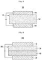
- FIGS. 1 and 2 are cross-sectional views showing organic light emitting diodes according to one embodiment, respectively.
- substituted refers to one substituted with a deuterium, a halogen, a hydroxy group, an amino group, a substituted or unsubstituted C1 to C30 amine group, a nitro group, a substituted or unsubstituted C1 to C40 silyl group, C1 to C30 alkyl group, a C1 to C10 alkylsilyl group, a C3 to C30 cycloalkyl group, a C3 to C30 heterocycloalkyl group, a C6 to C30 aryl group, a C6 to C30 heteroaryl group, a C1 to C20 alkoxy group, a fluoro group, a C1 to C10 trifluoroalkyl group such as a trifluoromethyl group, or a cyano group, instead of at least one hydrogen of a substituent or a compound.
- the substituted C6 to C30 aryl group may be fused with another adjacent substituted C6 to C30 aryl group to form a substituted or unsubstituted fluorene ring.
- hetero refers to one including 1 to 3 hetero atoms selected from the group consisting of N, O, S, P, and Si, and remaining carbons in one compound or substituent.
- alkyl group refers to an aliphatic hydrocarbon group.
- the alkyl group may be "a saturated alkyl group” without any double bond or triple bond.
- the alkyl group may be a C1 to C30 alkyl group. More specifically, the alkyl group may be a C1 to C20 alkyl group or a C1 to C10 alkyl group.
- a C1 to C4 alkyl group may have 1 to 4 carbon atoms in an alkyl chain which may be selected from methyl, ethyl, propyl, iso-propyl, n-butyl, iso-butyl, sec-butyl, and t-butyl.
- alkyl group may be a methyl group, an ethyl group, a propyl group, an isopropyl group, a butyl group, an isobutyl group, a t-butyl group, a pentyl group, a hexyl group, a cyclopropyl group, a cyclobutyl group, a cyclopentyl group, a cyclohexyl group, and the like.
- aryl group refers to a cyclic substituent where all elements have p-orbitals, and these p-orbitals forms conjugation, and includes a monocyclic, polycyclic or fused ring polycyclic (i.e., rings sharing adjacent pairs of carbon atoms) functional group.
- heteroaryl group refers to aryl group including 1 to 3 hetero atoms selected from N, O, S, P and Si, and remaining carbons.
- heteroaryl group is a fused ring, each ring may include 1 to 3 hetero atoms.
- the substituted or unsubstituted C6 to C30 aryl group and/or the substituted or unsubstituted C2 to C30 heteroaryl group refer to a substituted or unsubstituted phenyl group, a substituted or unsubstituted naphthyl group, a substituted or unsubstituted anthracenyl group, a substituted or unsubstituted phenanthryl group, a substituted or unsubstituted naphthacenyl group, a substituted or unsubstituted pyrenyl group, a substituted or unsubstituted biphenyl group, a substituted or unsubstituted p-terphenyl group, a substituted or unsubstituted m-terphenyl group, a substituted or unsubstituted chrysenyl group, a substituted or unsubstituted triphenylenyl group, a
- hole characteristics refer to characteristics to donate an electron and to form a hole when an electric field is applied, and characteristics that holes formed in the anode is easily injected into the emission layer and transported in the emission layer due to conductive characteristics according to HOMO level.
- Electron characteristics refer to characteristics to accept an electron when an electric field is applied, and characteristics that electron formed in the cathode is easily injected into the emission layer and transported in the emission layer due to conductive characteristics according to LUMO level.
- the composition according to one embodiment includes at least two kinds of hosts and dopant, wherein the hosts include a first host compound having bipolar characteristics and a second host compound having hole characteristics and at least two fused rings.
- the first host compound is represented by Chemical Formula I.
- X 1 is O, Se, S, SO, SO 2 , PO, or CO
- X 2 is CR a R b or SiR c R d
- R 1 to R 5 and R a to R d are each independently hydrogen, deuterium, a substituted or unsubstituted C1 to C30 alkyl group, a substituted or unsubstituted C3 to C30 cycloalkyl group, a substituted or unsubstituted C3 to C30 heterocycloalkyl group, a substituted or unsubstituted C6 to C30 aryl group, a substituted or unsubstituted C3 to C30 heteroaryl group, a substituted or unsubstituted amine group, a substituted or unsubstituted C6 to C30 arylamine group, a substituted or unsubstituted C3 to C30 heteroarylamine group, a substituted or un
- the first host compound may be for example represented by one of Chemical Formulae 1 a to 1 c according to a bonding position of a substituent.
- the first host compound may be for example represented by one of Chemical Formulae 1-1 to 1-6.
- R 1 to R 5 are the same as described above, for example R 1 to R 5 are each independently hydrogen, deuterium, a substituted or unsubstituted C1 to C20 alkyl group, a substituted or unsubstituted C6 to C30 aryl group, a substituted or unsubstituted C3 to C30 heteroaryl group, or a combination thereof.
- At least one of R 1 to R 5 and R a to R d of In Chemical Formula I, Chemical Formulae 1 a to 1c and Chemical Formulae 1-1 to 1-6 may be a substituent having hole characteristics or electron characteristics, and may be, for example selected from a substituted or unsubstituted functional group listed in Group 1.
- Y is N, O, S, SO 2 , NRj, CR k , SiR l , CR m R n or SiR o R p
- Z is N, CR q , CR r R s , or NR t
- R j to R t are each independently hydrogen, deuterium, a substituted or unsubstituted C1 to C20 alkyl group, a substituted or unsubstituted C6 to C30 aryl group, a substituted or unsubstituted C3 to C30 heteroaryl group, or a combination thereof
- Ar5 is a single bond, a substituted or unsubstituted C1 to C20 alkylene group, a substituted or unsubstituted C2 to C20 alkenylene group, a substituted or unsubstituted C6 to C30 arylene group, a substituted or unsubstituted C2 to C30 heteroarylene group,
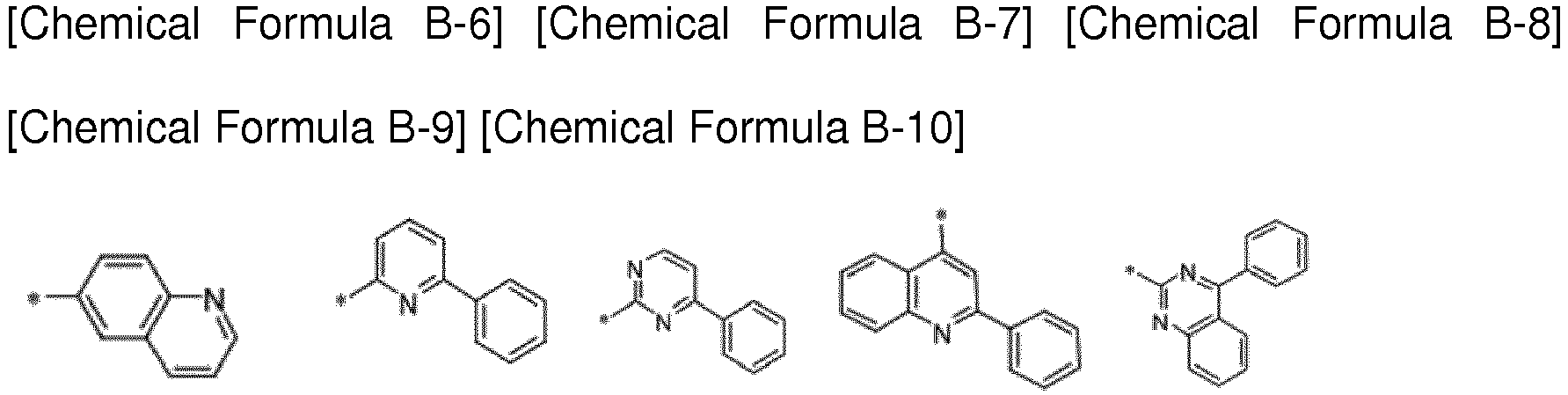
- the substituted or unsubstituted functional group of Group 1 may be, for example selected from Chemical Formulae B-1 to B-35.
- the first host compound may be for example represented in [Table 1] and [Table 2], and herein, the substituent indicates R 1 when a core moiety is 1-1 and 1-2 and the substituent indicates R 3 when the core moiety is 1-3 to 1-6, and particularly, other non-mentioned substituents are all hydrogen.
- Table 1 Compound Nos. Core moiety Substituent Compound Nos. Core moiety Substituent Compound Nos.
- the first host compound may be, for example, represented by one of Chemical Formulae 1-A to 1-P.
- the second host compound may be represented by Chemical Formula II.
- X 3 is O, S, CR u R v , SiR w R x , or NR y
- HTU is a substituted or unsubstituted carbazolyl group or a substituted or unsubstituted triphenylenyl group
- R 11 to R 13 and R u to R y are each independently hydrogen, deuterium, a substituted or unsubstituted C1 to C20 alkyl group, a substituted or unsubstituted C6 to C30 aryl group, a substituted or unsubstituted C3 to C30 heteroaryl group, or a combination thereof.
- the second host compound may be, for example a compound including two carbazole groups represented by Chemical Formula 2.
- Ar 1 , Ar 2 , and R 11 to R 16 are the same as R 1 to R 5 , for example Ar 1 , Ar 2 and R 11 to R 16 are each independently hydrogen, deuterium, a substituted or unsubstituted C1 to C20 alkyl group, a substituted or unsubstituted C6 to C30 aryl group, a substituted or unsubstituted C3 to C30 heteroaryl group, or a combination thereof.
- the compound represented by Chemical Formula 2 may be for example represented by one of Chemical Formulae 2-1 to 2-3 according to a bonding position of a substituent.
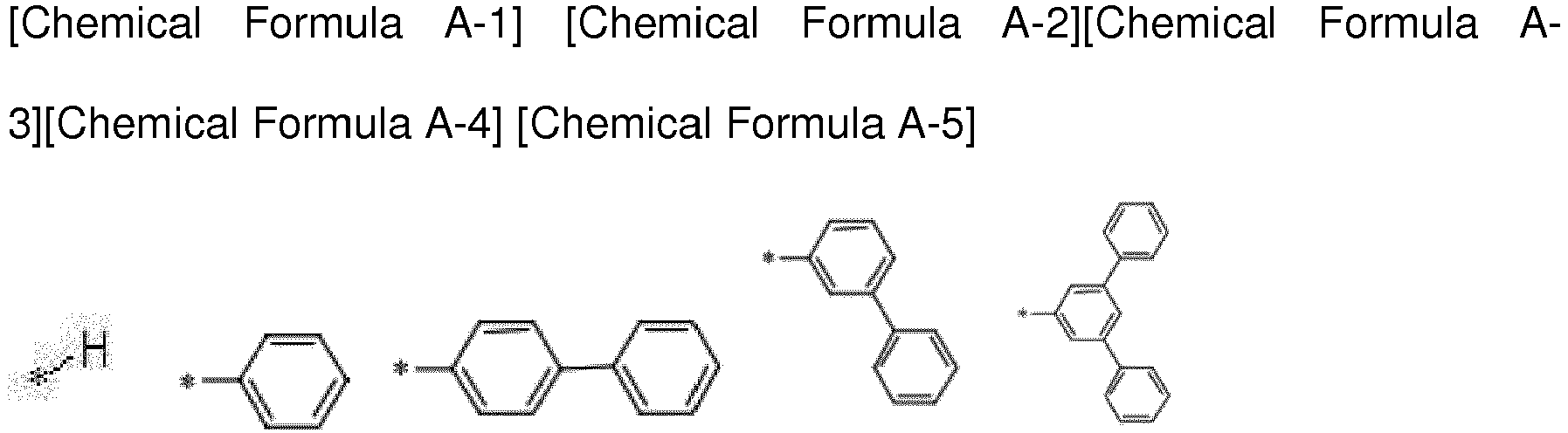
- At least one of Ar 1 , Ar 2 , and R 11 to R 16 of Chemical Formula 2 and Chemical Formulae 2-1 to 2-3 may be a substituent having hole characteristics, for example a substituent selected from Chemical Formulae A-1 to A-15.
- the compound represented by Chemical Formula 2 may be, for example represented in [Table 3] to [Table 5], wherein substituents that is not mentioned, R 11 to R 16 are all hydrogen. (Table 3) Comp -ound Nos. Core Substit -uent Ar1 Substit -uent Ar2 Comp -ound Nos. Core Substit -uent Ar1 Substit -uent Ar2 Comp -ound Nos.
- Core Substituent Ar1 Substituent Ar2 Compound Nos. Core Substituent Ar1 Substituent Ar2 441 2-3 A-4 A-7 481 2-3 A-8 A-9 442 2-3 A-4 A-8 482 2-3 A-8 A-10 443 2-3 A-4 A-9 483 2-3 A-8 A-11 444 2-3 A-4 A-10 484 2-3 A-8 A-12 445 2-3 A-4 A-11 485 2-3 A-8 A-13 446 2-3 A-4 A-12 486 2-3 A-8 A-14 447 2-3 A-4 A-13 487 2-3 A-8 A-15 448 2-3 A-4 A-14 488 2-3 A-9 A-9 449 2-3 A-4 A-15 489 2-3 A-9 A-10 450 2-3 A-5 A-5 490 2-3 A-9 A-11 451 2-3 A-5 A-6 491 2-3 A-9 A-12 452 2-3 A-5 A-7 492 2-3 A-9 A-13 453 2-3 A-5 A-8 493 2-3 A-9 A-14 454 2-3 A-5 A-9 494 2-3 A-9 A-15 455 2-3 A-5 A-10 495 2-3 A-10 A-10 456 2-3 A-5 A-11 496
- the compound represented by Chemical Formula 2 may be, for example represented by Chemical Formula 2-A to 2-C.
- the second host compound may be, for example a compound represented by Chemical Formula 3.
- X 3 is O, S, CR e R f , SiR g R h , or NR i
- L is a single bond, a substituted or unsubstituted C1 to C20 alkylene group, a substituted or unsubstituted C2 to C20 alkenylene group, a substituted or unsubstituted C6 to C30 arylene group, a substituted or unsubstituted C2 to C30 heteroarylene group, or a combination thereof
- R 11 to R 13 , R 17 to R 21 , and R e to R i are each independently hydrogen, deuterium, a substituted or unsubstituted C1 to C20 alkyl group, a substituted or unsubstituted C6 to C30 aryl group, a substituted or unsubstituted C3 to C30 heteroaryl group, or a combination thereof.
- the compound represented by Chemical Formula 3 may be, for example represented by Chemical Formula 3a according to a bonding position.
- the compound represented by Chemical Formula 3 may be, for example represented by one of Chemical Formulae 3-1 to 3-10.
- R 11 to R 13 , R 17 to R 21 , and R i are the same as described above.
- At least one among R 11 to R 13 , R 17 to R 21 , and R e to R i in Chemical Formulae 3, 3a, and 3-1 to 3-10 may be a substituent having one hole, for example, a substituent selected from Chemical Formulae A-1 to A-15.
- the compound represented by Chemical Formula 3 may be, for example, represented in [Table 6] and [Table 7], wherein the substituent indicates R 11 when a core moiety is 3-1 to 3-8 and the substituent indicates R i when the core moiety is 3-9 and 3-10, and particularly, other non-mentioned substituents are all hydrogen.
- Table 6 Compound Nos. Core moiety Substituent Compound Nos. Core moiety Substituent Compound Nos.
- the compound represented by Chemical Formula 3 may be for example represented by one of Chemical Formulae 3-A to 3-E.
- the first and second host compounds may be variously mixed to prepare various compositions.
- the composition may include the first host compound and the second host compound represented by Chemical Formula 2
- another composition may include the first host compound and the third host compound represented by Chemical Formula 3.
- the composition may include a compound selected from compounds shown in Chemical Formula I in Tables 1 and 2 as a first host compound and a compound represented by Chemical Formula 2 in Tables 3 to 5 or a compound represented by Chemical Formula 3 in Tables 6 and 7 as a second host compound.
- the compounds listed in Tables 1 to 7 show various first host and second host compounds, but are not limited thereto.
- the first host compound simultaneously has electron characteristics, and the second host compound has hole characteristics, these two compouns may be included together to realize bipolar characteristics. Accordingly, when the composition is used to form an emission layer for an organic optoelectronic device, satisfactory interface characteristics and hole and electron-transporting capability may be improved.
- the first and second host compounds may be, for example, included in a weight ratio of about 1:10 to about 10:1.
- bipolar characteristics and improve efficiency and a life-span may be realized by suing electron transport capability of the first host compound and hole transport capability of the second host compound in an appropriate ratio to form an emission layer.
- composition may further include at least one host compound in addition to the first host compound and the second host compound.
- the composition may further include a dopant.
- the dopant may be a red, green, or blue dopant, for example, a phosphorescent dopant.
- the dopant is mixed with the first host compound and the second host compound in a small amount to cause light emission, and may be generally a material such as a metal complex that emits light by multiple excitation into a triplet or more.
- the dopant may be, for example an inorganic, organic, or organic/inorganic compound, and one or more kinds thereof may be used.
- Examples of the phosphorescent dopant may be an organic metal compound including Ir, Pt, Os, Ti, Zr, Hf, Eu, Tb, Tm, Fe, Co, Ni, Ru, Rh, Pd or a combination thereof.
- the phosphorescent dopant may be, for example compounds represented by Chemical Formulae A to C, but is not limited thereto.
- the composition may form a film using a dry film-forming method such as chemical vapor deposition.
- the organic optoelectronic device may be any device to convert electrical energy into photoenergy and vice versa without particular limitation, and may be, for example an organic photoelectric device, an organic light emitting diode, an organic solar cell, and an organic photo-conductor drum.
- FIGS. 1 and 2 are cross-sectional views of each organic light emitting diode according to one embodiment.
- an organic optoelectronic device 100 includes an anode 120 and a cathode 110 facing each other and an organic layer 105 interposed between the anode 120 and cathode 110.
- the anode 120 may be made of a conductor having a high work function to help hole injection, and may be for example metal, metal oxide and/or a conductive polymer.
- the anode 120 may be, for example a metal nickel, platinum, vanadium, chromium, copper, zinc, gold, and the like or an alloy thereof; metal oxide such as zinc oxide, indium oxide, indium tin oxide (ITO), indium zinc oxide (IZO), and the like; a combination of metal and oxide such as ZnO and Al or SnO2 and Sb; a conductive polymer such as poly(3-methylthiophene), poly(3,4-(ethylene-1,2-dioxy)thiophene) (PEDT), polypyrrole, and polyaniline, but is not limited thereto.
- the cathode 110 may be made of a conductor having a low work function to help electron injection, and may be for example metal, metal oxide and/or a conductive polymer.
- the cathode 110 may be for example a metal or an alloy thereof such as magnesium, calcium, sodium, potassium, titanium, indium, yttrium, lithium, gadolinium, aluminum silver, tin, lead, cesium, barium, and the like; a multi-layer structure material such as LiF/AL, LiO 2 /Al, LiF/Ca, LiF/Al and BaF 2 /Ca, but is not limited thereto.
- the organic layer 105 includes an emission layer 130 including the above-mentioned composition.
- the emission layer 130 may include for example the above-mentioned composition.
- an organic light emitting diode 200 further includes a hole auxiliary layer 140 as well as an emission layer 130.
- the hole auxiliary layer 140 may further increase hole injection and/or hole mobility between the anode 120 and emission layer 130 and block electrons.
- the hole auxiliary layer 140 may be, for example a hole transport layer, a hole injection layer, and/or an electron blocking layer, and may include at least one layer.
- an organic light emitting diode may further include an electron transport layer, an electron injection layer (EIL), a hole injection layer, and the like, as an organic thin layer 105 in FIG. 1 or FIG. 2 .
- EIL electron injection layer
- hole injection layer hole injection layer
- the organic light emitting diodes 100 and 200 may be manufactured by forming an anode or a cathode on a substrate, forming an organic layer in accordance with a dry coating method such as evaporation, sputtering, plasma plating, and ion plating; and forming a cathode or an anode thereon.
- a dry coating method such as evaporation, sputtering, plasma plating, and ion plating
- the organic light emitting diode may be applied to an organic light emitting diode (OLED) display.
- OLED organic light emitting diode
- the intermediate (B) was dissolved in 250 ml of dichloromethane, and the solution was cooled down to 0 °C and agitated. Then, borontrifluoride dissolved in 20 mL of dichloromethane and 12.84 g (47.5 mmol) of diethyl ether complex were slowly added thereto, and the mixture was agitated at room temperature for 5 hours. When the reaction was complete, the resultant was extracted with ethylacetate, an extract was dried with magnesium sulfate, filtered, and concentrated under a reduced pressure. Then, a product therefrom was purified with n-Hexane through silica gel column chromatography, obtaining 22 g (yield of 71.9 %) of a desired compound, an intermediate (C) as a white solid.
- reaction solution was cooled down to -78 °C, 68.17 mL (295.41 mmol) of triisopropyl borate was slowly added thereto, and the mixture was agitated at room temperature for 12 hours.
- the reaction was completed with a 3N HCl aqueous solution, the resultant was extracted with ethylacetate, and an extracted was dried with magnesium sulfate, dried, filtered, and concentrated under a reduced pressure. Then, a product therefrom was purified with a silica gel filter, obtaining 62.5 g (a yield of 77 %) of a desired compound, an intermediate 1-1.
- the resultant was concentrated under a reduced pressure to remove a solvent therein and extracted with distilled water and dichloromethane, an extract was dried with magnesium sulfate and filtered, and the filtered solution was concentrated under a reduced pressure, obtaining a desired compound, an intermediate (E) as a liquid having high viscosity.
- the intermediate (E) was dissolved in 250 ml of dichloromethane, and the solution was cooled down to 0 °C and agitated. Then, borontrifluoride dissolved in 20 mL of dichloromethane and 12.6 g (47.1 mmol) of a diethyl ether complex were slowly added thereto, and the mixture was agitated at room temperature for 5 hours. When the reaction was complete, the resultant was extracted with ethylacetate, an extract was dried with magnesium sulfate and filtered, and a filtered solution was concentrated under a reduced pressure. Then, a product therefrom was purified with n-hexane through silica gel column chromatography, obtaining 10.5 g (a yield of 74.3 %) of a desired compound, an intermediate (F) as a white solid.
- reaction solution was cooled down to -78 °C, 8.8 mL (38.15 mmol) of triisopropyl borate was slowly added thereto, and the mixture was agitated at room temperature for 12 hours.
- the reaction was completed with a 3N HCl aqueous solution, the resultant was extracted with ethylacetate, and an extract was dried with magnesium sulfate, filtered, and concentracted under a reduced pressure. Then, a product therefrom was purified with a silica gel filter, obtaining 8.47 g (a yield of 77 %) of a desired compound, an intermediate 1-2.
- the solution was concentrated under a reduced pressure to remove a solvent therefrom and then, extracted with distilled water and dichloromethane, and an extract obtained therefrom was dried with anhydrous magnesium sulfate, filtered, and concentrated under a reduced pressure, obtaining a desired compound, an intermediate (H) as a liquid having high viscosity.
- the intermediate (H) was dissolved in 250 ml of dichloromethane, and the solution was cooled down to 0 °C and agitated. Then, borontrifluoride dissolved in 20 mL of dichloromethane and 15.18 g (56.7 mmol) of a diethyl ether complex were slowly added thereto, and the mixture was agitated at room temperature for 5 hours. When the reaction was complete, the resultant was extracted with ethylacetate, an extract was dried with magnesium sulfate, filtered, and concentrated under a reduced pressure. Then, a product therefrom was purified with n-hexane through silica gel column chromatography, obtaining 29 g (a yield of 80 %) of a desired compound, an intermediate (I) as a white solid.
- reaction solution was cooled down to -78 °C, 7.61 mL (109.16 mmol) of trimethyl borate was slowly added thereto, and the mixture was agitated at room temperature for 12 hours.
- the reaction was completed by a 3N HCl aqueous solution and extracted with ethylacetate, and an extract was dried with magnesium sulfate, filtered, and concentrated under a reduced pressure. Then, a product therefrom was purified with a silica gel filter, obtaining 23 g (a yield of 77 %) of a desired compound, an intermediate 1-3.
- An intermediate 1-4 was synthesized by using (4-dibenzothienyl)boronic acid as a synthesis starting material through the same steps in Reaction Scheme 4 as the intermediate 1-3.
- An intermediate 1-5 was synthesized by using methyl-2-bromo-4-chlorobenzoate as a synthesis starting material through the same steps in Reaction Scheme 4 as the intermediate 1-3.
- An intermediate 1-6 was synthesized by using (4-dibenzothienyl)boronic acid as a synthesis starting material through the same steps in Reaction Scheme 6 as the intermediate 1-5.
- a compound was prepared according to the same method as above except for using two starting materials provided in the following Table instead of Phenylcarbazolylbromide (corresponding to a starting material 1 in Table 9) and phenylcarbazolylboronic acid (corresponding to a starting material 2 in Table 9) of Example 17.
- Table 9 Ex Starting material 1 Starting material 2 Product Yield (%) LC-Mass (H+H + ) 18 90 % 561.23 19 85 % 637.27
- the anode As for an anode, 1000 ⁇ -thick ITO was used, and as for a cathode, 1000 ⁇ -thick aluminum (Al) was used.
- the anode is manufactured by cutting an ITO glass substrate having 15 ⁇ /cm 2 of sheet resistance into a size of 50 mm ⁇ 50 mm ⁇ 0.7 mm, ultrasonic wave-cleaning them in acetone, isopropylalcohol, and pure water for 15 minutes respectively, and UV ozone cleaning them for 30 minutes.
- an 800 ⁇ -thick hole transport layer (HTL) was formed by depositing N4,N4'-di(naphthalen-1-yl)-N4,N4'-diphenylbiphenyl-4,4'-diamine (NPB) under a vacuum degree 650 ⁇ 10 -7 Pa at a deposit speed of 0.1 to 0.3 nm/s.
- a 300 ⁇ -thick emission layer was formed through a vacuum depositon by mixing the compound 1-F of Example 1 and the compound 2-A of Example 17 which are obtained under the same vacuum deposit conditio in a weight ratio of 1:1 as a host and simultaneously, doping the mixture with a phosphorescent dopant of Ir(ppy)3.
- the phosphorescent dopant was deposited in an amount of 10 wt% based on 100 wt% of the total amount of the emission layer by adjusting its deposit speed.
- a 50 ⁇ -thick hole blocking layer was formed by depositing bis(2-methyl-8-quinolinolate)-4-(phenylphenolato)aluminium (BAIq) under the same vacuum deposit condition.
- BAIq bis(2-methyl-8-quinolinolate)-4-(phenylphenolato)aluminium
- a 250 ⁇ -thick electron transport layer was formed by depositing Alq3 under the same vacuum deposit condition.
- a cathode was formed by sequentially depositing LiF and Al, manufacturing an organic photoelectric device.
- the organic photoelectric device had a structure of ITO/ NPB (80 nm)/ EML (compound 1-F (45 wt%) + compound 2-A (45 wt%) + Ir(PPy)3 (10 wt%), 30 nm)/ Balq (5 nm)/ Alq3 (25 nm)/ LiF (1 nm) / Al (100 nm).
- An organic light emitting diode was manufactured according to the same method as Example 25 except for using the compound 1-F and the compound 2-A in a ratio of 4:1 instead of mixing the compound 1-F and the compound 2-A in a weight ratio of 1:1.
- An organic light emitting diode was manufactured according to the same method as Example 25 except for using the compound 1-F and the compound 2-A in a ratio of 1:4 instead of mixing the compound 1-F and the compound 2-A in a weight ratio of 1:1.
- An organic light emitting diode was manufactured according to the same method as Example 25 except for depositing the compound 1-N according to Example 14 and the compound 2-A in a ratio of 1:1 instead of mixing the compound 1-F and the compound 2-A in a weight ratio of 1:1.
- An organic light emitting diode was manufactured according to the same method as Example 28 except for depositing the compound 1-N and the compound 2-A in a ratio of 4:1 instead of mixing the compound 1-N and the compound 2-A in a weight ratio of 1:1.
- An organic light emitting diode was manufactured according to the same method as Example 28 except for depositing the compound 1-N and the compound 2-A in a ratio of 1:4 instead of mixing the compound 1-N and the compound 2-A in a weight ratio of 1:1.
- An organic light emitting diode was manufactured according to the same method as Example 28 except for depositing the compound 1-N and the compound 3-A according to Example 22 in a ratio of 1:1 instead of mixing the compound 1-N and the compound 2-A in a weight ratio of 1:1.
- An organic light emitting diode was manufactured according to the same method as Example 31 except for depositing the compound 1-N and the compound 3-A in a ratio of 4:1 instead of mixing the compound 1-N and the compound 3-A in a weight ratio of 1:1.
- An organic light emitting diode was manufactured according to the same method as Example 31 except for depositing the compound 1-N and the compound 3-A in a ratio of 1:4 instead of mixing the compound 1-N and the compound 3-A in a weight ratio of 1:1.
- An organic light emitting diode was manufactured according to the same method as Example 25 except for depositing the compound 1-F as a single host instead of mixing the compound 1-F and the compound 2-A in a weight ratio of 1:1.
- An organic light emitting diode was manufactured according to the same method as Example 28 except for depositing the compound 1-N as a single host instead of mixing the compound 1-N and the compound 2-A in a weight ratio of 1:1.
- An organic light emitting diode was manufactured according to the same method as Example 28 except for depositing the compound 2-A as a single host instead of mixing the compound 1-N and the compound 2-A in a weight ratio of 1:1.
- An organic light emitting diode was manufactured according to the same method as Example 31 except for depositing the compound 3-A as a host instead of mixing the compound 1-N and the compound 2-A in a weight ratio of 1:1.
- Luminance of the manufactured organic light emitting diodes was measured for luminance, while increasing the voltage from 0 V to 10 V using a luminance meter (Minolta Cs-1000A).
- the organic light emitting diodes according to Examples 25 to 33 showed remarkably improved luminous efficiency or/ life-span compared with the organic light emitting diodes according to Comparative Examples 1 to 4.
- the organic light emitting diode according to Example 31 showed improved efficiency and superbly improved life-span compared with the organic light emitting diodes according to Comparative Examples 2 and 4. The reason is that the efficiency and the life-span were improved by bipolar characteristics of a hole-transporting host and an electron-transporting host.
Landscapes
- Chemical & Material Sciences (AREA)
- Organic Chemistry (AREA)
- Engineering & Computer Science (AREA)
- Materials Engineering (AREA)
- Physics & Mathematics (AREA)
- Spectroscopy & Molecular Physics (AREA)
- Optics & Photonics (AREA)
- Electroluminescent Light Sources (AREA)
- Plural Heterocyclic Compounds (AREA)
- Furan Compounds (AREA)
- Indole Compounds (AREA)
Abstract
Description
- A composition, an organic optoelectronic device and a display device are disclosed.
- An organic optoelectronic device is a device that converts electrical energy into photoenergy, and vice versa.
- An organic optoelectronic device may be classified as follows in accordance with its driving principles. One is an optoelectronic device where excitons are generated by photoenergy, separated into electrons and holes, and are transferred to different electrodes to generate electrical energy, and the other is a light emitting device where a voltage or a current is supplied to an electrode to generate photoenergy from electrical energy.
- Examples of the organic optoelectronic device may be an organic photoelectric device, an organic light emitting diode, an organic solar cell, and an organic photo conductor drum.
- Of these, an organic light emitting diode (OLED) has recently drawn attention due to an increase in demand for flat panel displays. Such an organic light emitting diode converts electrical energy into light by applying current to an organic light emitting material. It has a structure in which an organic layer is interposed between an anode and a cathode. Herein, the organic layer may include an emission layer and optionally an auxiliary layer, and the auxiliary layer may be, for example at least one selected from a hole injection layer, a hole transport layer, an electron blocking layer, an electron transport layer, an electron injection layer, and a hole blocking layer for improving efficiency and stability of an organic light emitting diode.
- Performance of an organic light emitting diode may be affected by characteristics of the organic layer, and among them, may be mainly affected by characteristics of an organic material of the organic layer.
- Particularly, development for an organic material being capable of increasing hole and electron mobility and simultaneously increasing electrochemical stability is needed so that the organic light emitting diode may be applied to a large-size flat panel display.
- One embodiment provides a composition for an organic optoelectronic device being capable of realizing an organic optoelectronic device having high efficiency and long life-span.
- Another embodiment provides an organic optoelectronic device including the composition.
- Yet another embodiment provides a display device including the organic optoelectronic device.
- According to one embodiment, a composition includes a first host compound represented by Chemical Formula I and a second host compound represented by Chemical Formula II.

X1 is O, Se, S, SO, SO2, PO, or CO,
X2 is CRaRb or SiRcRd, and
R1 to R5 and Ra to Rd are each independently hydrogen, deuterium, a substituted or unsubstituted C1 to C30 alkyl group, a substituted or unsubstituted C3 to C30 cycloalkyl group, a substituted or unsubstituted C3 to C30 heterocycloalkyl group, a substituted or unsubstituted C6 to C30 aryl group, a substituted or unsubstituted C3 to C30 heteroaryl group, a substituted or unsubstituted amine group, a substituted or unsubstituted C6 to C30 arylamine group, a substituted or unsubstituted C3 to C30 heteroarylamine group, a substituted or unsubstituted C1 to C30 alkoxy group, a substituted or unsubstituted C2 to C30 alkoxycarbonyl group, a substituted or unsubstituted C2 to C30 alkoxycarbonylamino group, a substituted or unsubstituted C7 to C30 aryloxycarbonylamino group, a substituted or unsubstituted C1 to C30 sulfamoylamino group, a substituted or unsubstituted C2 to C30 alkenyl group, a substituted or unsubstituted C2 to C30 alkynyl group, a substituted or unsubstituted silyl group, a substituted or unsubstituted silyloxy group, a substituted or unsubstituted C1 to C30 acyl group, a substituted or unsubstituted C1 to C20 acyloxy group, a substituted or unsubstituted C1 to C20 acylamino group, a substituted or unsubstituted C1 to C30 sulfonyl group, a substituted or unsubstituted C1 to C30 alkylthiol group, a substituted or unsubstituted C1 to C30 heterocyclothiol group, a substituted or unsubstituted C6 to C30 arylthiol group, a substituted or unsubstituted C1 to C30 heteroarylthiol group, a substituted or unsubstituted C1 to C30 ureide group, a halogen, a halogen-containing group, a cyano group, a hydroxyl group, an amino group, a nitro group, a carboxyl group, a ferrocenyl group, or a combination thereof.
X3 is O, S, CRuRv, SiRwRx, or NRy,
HTU is a substituted or unsubstituted carbazolyl group or a substituted or unsubstituted triphenylenyl group, and
R11 to R13 and Ru to Ry are each independently hydrogen, deuterium, a substituted or unsubstituted C1 to C20 alkyl group, a substituted or unsubstituted C6 to C30 aryl group, a substituted or unsubstituted C3 to C30 heteroaryl group, or a combination thereof. - According to another embodiment, an organic optoelectronic device includes an anode and a cathode facing each other, at least one organic layer between the anode and the cathode, wherein the organic layer includes the composition.
- According to yet another embodiment, a display device including the organic optoelectronic device is provided.
- An organic optoelectronic device having high efficiency and long life-span may be realized.
-
FIGS. 1 and 2 are cross-sectional views showing organic light emitting diodes according to one embodiment, respectively. - Hereinafter, embodiments of the present invention are described in detail. However, these embodiments are exemplary, the present invention is not limited thereto and the present invention is defined by the scope of claims.
- In the present specification, when a definition is not otherwise provided, the term "substituted" refers to one substituted with a deuterium, a halogen, a hydroxy group, an amino group, a substituted or unsubstituted C1 to C30 amine group, a nitro group, a substituted or unsubstituted C1 to C40 silyl group, C1 to C30 alkyl group, a C1 to C10 alkylsilyl group, a C3 to C30 cycloalkyl group, a C3 to C30 heterocycloalkyl group, a C6 to C30 aryl group, a C6 to C30 heteroaryl group, a C1 to C20 alkoxy group, a fluoro group, a C1 to C10 trifluoroalkyl group such as a trifluoromethyl group, or a cyano group, instead of at least one hydrogen of a substituent or a compound.
- In addition, two adjacent substituents of the halogen, hydroxy group, amino group, substituted or unsubstituted C1 to C20 amine group, nitro group, substituted or unsubstituted C3 to C40 silyl group, C1 to C30 alkyl group, C1 to C10 alkylsilyl group, C3 to C30 cycloalkyl group, C3 to C30 heterocycloalkyl group, C6 to C30 aryl group, C6 to C30 heteroaryl group, C1 to C20 alkoxy group, fluoro group, C1 to C10 trifluoroalkyl group such as trifluoromethyl group and the like, or cyano group may be fused with each other to form a ring. For example, the substituted C6 to C30 aryl group may be fused with another adjacent substituted C6 to C30 aryl group to form a substituted or unsubstituted fluorene ring.
- In the present specification, when specific definition is not otherwise provided, "hetero" refers to one including 1 to 3 hetero atoms selected from the group consisting of N, O, S, P, and Si, and remaining carbons in one compound or substituent.
- In the present specification, when a definition is not otherwise provided, "alkyl group" refers to an aliphatic hydrocarbon group. The alkyl group may be "a saturated alkyl group" without any double bond or triple bond.
- The alkyl group may be a C1 to C30 alkyl group. More specifically, the alkyl group may be a C1 to C20 alkyl group or a C1 to C10 alkyl group. For example, a C1 to C4 alkyl group may have 1 to 4 carbon atoms in an alkyl chain which may be selected from methyl, ethyl, propyl, iso-propyl, n-butyl, iso-butyl, sec-butyl, and t-butyl.
- Specific examples of the alkyl group may be a methyl group, an ethyl group, a propyl group, an isopropyl group, a butyl group, an isobutyl group, a t-butyl group, a pentyl group, a hexyl group, a cyclopropyl group, a cyclobutyl group, a cyclopentyl group, a cyclohexyl group, and the like.
- In the present specification, "aryl group" refers to a cyclic substituent where all elements have p-orbitals, and these p-orbitals forms conjugation, and includes a monocyclic, polycyclic or fused ring polycyclic (i.e., rings sharing adjacent pairs of carbon atoms) functional group.
- In the present specification, "heteroaryl group" refers to aryl group including 1 to 3 hetero atoms selected from N, O, S, P and Si, and remaining carbons. When the heteroaryl group is a fused ring, each ring may include 1 to 3 hetero atoms.
- More specifically, the substituted or unsubstituted C6 to C30 aryl group and/or the substituted or unsubstituted C2 to C30 heteroaryl group refer to a substituted or unsubstituted phenyl group, a substituted or unsubstituted naphthyl group, a substituted or unsubstituted anthracenyl group, a substituted or unsubstituted phenanthryl group, a substituted or unsubstituted naphthacenyl group, a substituted or unsubstituted pyrenyl group, a substituted or unsubstituted biphenyl group, a substituted or unsubstituted p-terphenyl group, a substituted or unsubstituted m-terphenyl group, a substituted or unsubstituted chrysenyl group, a substituted or unsubstituted triphenylenyl group, a substituted or unsubstituted perylenyl group, a substituted or unsubstituted indenyl group, a substituted or unsubstituted furanyl group, a substituted or unsubstituted thiophenyl group, a substituted or unsubstituted pyrrolyl group, a substituted or unsubstituted pyrazolyl group, a substituted or unsubstituted imidazolyl group, a substituted or unsubstituted triazolyl group, a substituted or unsubstituted oxazolyl group, a substituted or unsubstituted thiazolyl group, a substituted or unsubstituted oxadiazolyl group, a substituted or unsubstituted thiadiazolyl group, a substituted or unsubstituted pyridyl group, a substituted or unsubstituted pyrimidinyl group, a substituted or unsubstituted pyrazinyl group, a substituted or unsubstituted triazinyl group, a substituted or unsubstituted benzofuranyl group, a substituted or unsubstituted benzothiophenyl group, a substituted or unsubstituted benzimidazolyl group, a substituted or unsubstituted indolyl group, a substituted or unsubstituted quinolinyl group, a substituted or unsubstituted isoquinolinyl group, a substituted or unsubstituted quinazolinyl group, a substituted or unsubstituted quinoxalinyl group, a substituted or unsubstituted naphthyridinyl group, a substituted or unsubstituted benzoxazinyl group, a substituted or unsubstituted benzthiazinyl group, a substituted or unsubstituted acridinyl group, a substituted or unsubstituted phenazinyl group, a substituted or unsubstituted phenothiazinyl group, a substituted or unsubstituted phenoxazinyl group, a substituted or unsubstituted fluorenyl group, a substituted or unsubstituted dibenzofuranyl group, a substituted or unsubstituted dibenzothiophenyl group, a substituted or unsubstituted carbazolyl group, or a combination thereof, but is not limited thereto.
- In the present specification, hole characteristics refer to characteristics to donate an electron and to form a hole when an electric field is applied, and characteristics that holes formed in the anode is easily injected into the emission layer and transported in the emission layer due to conductive characteristics according to HOMO level.
- Electron characteristics refer to characteristics to accept an electron when an electric field is applied, and characteristics that electron formed in the cathode is easily injected into the emission layer and transported in the emission layer due to conductive characteristics according to LUMO level.
- Hereinafter, a composition according to one embodiment is described.
- The composition according to one embodiment includes at least two kinds of hosts and dopant, wherein the hosts include a first host compound having bipolar characteristics and a second host compound having hole characteristics and at least two fused rings.
- The first host compound is represented by Chemical Formula I.

X1 is O, Se, S, SO, SO2, PO, or CO,
X2 is CRaRb or SiRcRd, and
R1 to R5 and Ra to Rd are each independently hydrogen, deuterium, a substituted or unsubstituted C1 to C30 alkyl group, a substituted or unsubstituted C3 to C30 cycloalkyl group, a substituted or unsubstituted C3 to C30 heterocycloalkyl group, a substituted or unsubstituted C6 to C30 aryl group, a substituted or unsubstituted C3 to C30 heteroaryl group, a substituted or unsubstituted amine group, a substituted or unsubstituted C6 to C30 arylamine group, a substituted or unsubstituted C3 to C30 heteroarylamine group, a substituted or unsubstituted C1 to C30 alkoxy group, a substituted or unsubstituted C2 to C30 alkoxycarbonyl group, a substituted or unsubstituted C2 to C30 alkoxycarbonylamino group, a substituted or unsubstituted C7 to C30 aryloxycarbonylamino group, a substituted or unsubstituted C1 to C30 sulfamoylamino group, a substituted or unsubstituted C2 to C30 alkenyl group, a substituted or unsubstituted C2 to C30 alkynyl group, a substituted or unsubstituted silyl group, a substituted or unsubstituted silyloxy group, a substituted or unsubstituted C1 to C30 acyl group, a substituted or unsubstituted C1 to C20 acyloxy group, a substituted or unsubstituted C1 to C20 acylamino group, a substituted or unsubstituted C1 to C30 sulfonyl group, a substituted or unsubstituted C1 to C30 alkylthiol group, a substituted or unsubstituted C1 to C30 heterocyclothiol group, a substituted or unsubstituted C6 to C30 arylthiol group, a substituted or unsubstituted C1 to C30 heteroarylthiol group, a substituted or unsubstituted C1 to C30 ureide group, a halogen, a halogen-containing group, a cyano group, a hydroxyl group, an amino group, a nitro group, a carboxyl group, a ferrocenyl group or a combination thereof. - The first host compound may be for example represented by one of Chemical Formulae 1 a to 1 c according to a bonding position of a substituent.


- In Chemical Formulae 1 a to 1c, X1, X2, R1 to R5 and Ra to Rd are the same as described above.
- The first host compound may be for example represented by one of Chemical Formulae 1-1 to 1-6.


R1 to R5 are the same as described above, for example R1 to R5 are each independently hydrogen, deuterium, a substituted or unsubstituted C1 to C20 alkyl group, a substituted or unsubstituted C6 to C30 aryl group, a substituted or unsubstituted C3 to C30 heteroaryl group, or a combination thereof. - At least one of R1 to R5 and Ra to Rd of In Chemical Formula I, Chemical Formulae 1 a to 1c and Chemical Formulae 1-1 to 1-6 may be a substituent having hole characteristics or electron characteristics, and may be, for example selected from a substituted or unsubstituted functional group listed in Group 1.

Y is N, O, S, SO2, NRj, CRk, SiRl, CRmRn or SiRoRp,
Z is N, CRq, CRrRs, or NRt,
wherein Rj to Rt are each independently hydrogen, deuterium, a substituted or unsubstituted C1 to C20 alkyl group, a substituted or unsubstituted C6 to C30 aryl group, a substituted or unsubstituted C3 to C30 heteroaryl group, or a combination thereof,
Ar5 is a single bond, a substituted or unsubstituted C1 to C20 alkylene group, a substituted or unsubstituted C2 to C20 alkenylene group, a substituted or unsubstituted C6 to C30 arylene group, a substituted or unsubstituted C2 to C30 heteroarylene group, a substituted or unsubstituted C6 to C30 arylamine group, a substituted or unsubstituted C2 to C30 heteroarylamine group, or a combination thereof,
Ar6 and Ar7 are independently substituted or unsubstituted C6 to C30 aryl group, a substituted or unsubstituted C3 to C30 heteroaryl group, or a combination thereof,
n1 and n2 are each independently 0 or 1, and
* is a linking point to Chemical Formula 1 and may be positioned at one of elements of the functional group. - The substituted or unsubstituted functional group of Group 1 may be, for example selected from Chemical Formulae B-1 to B-35.



- The first host compound may be for example represented in [Table 1] and [Table 2], and herein, the substituent indicates R1 when a core moiety is 1-1 and 1-2 and the substituent indicates R3 when the core moiety is 1-3 to 1-6, and particularly, other non-mentioned substituents are all hydrogen.
(Table 1) Compound Nos. Core moiety Substituent Compound Nos. Core moiety Substituent Compound Nos. Core moiety Substituent 1 1-1 B-1 41 1-2 B-6 81 1-3 B-11 2 1-1 B-2 42 1-2 B-7 82 1-3 B-12 3 1-1 B-3 43 1-2 B-8 83 1-3 B-13 4 1-1 B-4 44 1-2 B-9 84 1-3 B-14 5 1-1 B-5 45 1-2 B-10 85 1-3 B-15 6 1-1 B-6 46 1-2 B-11 86 1-3 B-16 7 1-1 B-7 47 1-2 B-12 87 1-3 B-17 8 1-1 B-8 48 1-2 B-13 88 1-3 B-18 9 1-1 B-9 49 1-2 B-14 89 1-3 B-19 10 1-1 B-10 50 1-2 B-15 90 1-3 B-20 11 1-1 B-11 51 1-2 B-16 91 1-3 B-21 12 1-1 B-12 52 1-2 B-17 92 1-3 B-22 13 1-1 B-13 53 1-2 B-18 93 1-3 B-23 14 1-1 B-14 54 1-2 B-19 94 1-3 B-24 15 1-1 B-15 55 1-2 B-20 95 1-3 B-25 16 1-1 B-16 56 1-2 B-21 96 1-3 B-26 17 1-1 B-17 57 1-2 B-22 97 1-3 B-27 18 1-1 B-18 58 1-2 B-23 98 1-3 B-28 19 1-1 B-19 59 1-2 B-24 99 1-3 B-29 20 1-1 B-20 60 1-2 B-25 100 1-3 B-30 21 1-1 B-21 61 1-2 B-26 101 1-3 B-31 22 1-1 B-22 62 1-2 B-27 102 1-3 B-32 23 1-1 B-23 63 1-2 B-28 103 1-3 B-33 24 1-1 B-24 64 1-2 B-29 104 1-3 B-34 25 1-1 B-25 65 1-2 B-30 105 1-3 B-35 26 1-1 B-26 66 1-2 B-31 106 1-4 B-1 27 1-1 B-27 67 1-2 B-32 107 1-4 B-2 28 1-1 B-28 68 1-2 B-33 108 1-4 B-3 29 1-1 B-29 69 1-2 B-34 109 1-4 B-4 30 1-1 B-30 70 1-2 B-35 110 1-4 B-5 31 1-1 B-31 71 1-3 B-1 111 1-4 B-6 32 1-1 B-32 72 1-3 B-2 112 1-4 B-7 33 1-1 B-33 73 1-3 B-3 113 1-4 B-8 34 1-1 B-34 74 1-3 B-4 114 1-4 B-9 35 1-1 B-35 75 1-3 B-5 115 1-4 B-10 36 1-2 B-1 76 1-3 B-6 116 1-4 B-11 37 1-2 B-2 77 1-3 B-7 117 1-4 B-12 38 1-2 B-3 78 1-3 B-8 118 1-4 B-13 39 1-2 B-4 79 1-3 B-9 119 1-4 B-14 40 1-2 B-5 80 1-3 B-10 120 1-4 B-15 (Table 2) Compound Nos. Core Substituent Compound Nos. Core Substituent 121 1-4 B-16 161 1-5 B-21 122 1-4 B-17 162 1-5 B-22 123 1-4 B-18 163 1-5 B-23 124 1-4 B-19 164 1-5 B-24 125 1-4 B-20 165 1-5 B-25 126 1-4 B-21 166 1-5 B-26 127 1-4 B-22 167 1-5 B-27 128 1-4 B-23 168 1-5 B-28 129 1-4 B-24 169 1-5 B-29 130 1-4 B-25 170 1-5 B-30 131 1-4 B-26 171 1-5 B-31 132 1-4 B-27 172 1-5 B-32 133 1-4 B-28 173 1-5 B-33 134 1-4 B-29 174 1-5 B-34 135 1-4 B-30 175 1-5 B-35 136 1-4 B-31 176 1-6 B-1 137 1-4 B-32 177 1-6 B-2 138 1-4 B-33 178 1-6 B-3 139 1-4 B-34 179 1-6 B-4 140 1-4 B-35 180 1-6 B-5 141 1-5 B-1 181 1-6 B-6 142 1-5 B-2 182 1-6 B-7 143 1-5 B-3 183 1-6 B-8 144 1-5 B-4 184 1-6 B-9 145 1-5 B-5 185 1-6 B-10 146 1-5 B-6 186 1-6 B-11 147 1-5 B-7 187 1-6 B-12 148 1-5 B-8 188 1-6 B-13 149 1-5 B-9 189 1-6 B-14 150 1-5 B-10 190 1-6 B-15 151 1-5 B-11 191 1-6 B-16 152 1-5 B-12 192 1-6 B-17 153 1-5 B-13 193 1-6 B-18 154 1-5 B-14 194 1-6 B-19 155 1-5 B-15 195 1-6 B-20 156 1-5 B-16 196 1-6 B-21 157 1-5 B-17 197 1-6 B-22 158 1-5 B-18 198 1-6 B-23 159 1-5 B-19 199 1-6 B-24 160 1-5 B-20 200 1-6 B-25 - The first host compound may be, for example, represented by one of Chemical Formulae 1-A to 1-P.


- The second host compound may be represented by Chemical Formula II.


X3 is O, S, CRuRv, SiRwRx, or NRy,
HTU is a substituted or unsubstituted carbazolyl group or a substituted or unsubstituted triphenylenyl group, and
R11 to R13 and Ru to Ry are each independently hydrogen, deuterium, a substituted or unsubstituted C1 to C20 alkyl group, a substituted or unsubstituted C6 to C30 aryl group, a substituted or unsubstituted C3 to C30 heteroaryl group, or a combination thereof. - The second host compound may be, for example a compound including two carbazole groups represented by Chemical Formula 2.

Ar1, Ar2, and R11 to R16 are the same as R1 to R5, for example Ar1, Ar2 and R11 to R16 are each independently hydrogen, deuterium, a substituted or unsubstituted C1 to C20 alkyl group, a substituted or unsubstituted C6 to C30 aryl group, a substituted or unsubstituted C3 to C30 heteroaryl group, or a combination thereof. - The compound represented by Chemical Formula 2 may be for example represented by one of Chemical Formulae 2-1 to 2-3 according to a bonding position of a substituent.

- In Chemical Formulae 2-1 to 2-3, Ar1, Ar2, and R11 to R16 are the same as described above.
- At least one of Ar1, Ar2, and R11 to R16 of Chemical Formula 2 and Chemical Formulae 2-1 to 2-3 may be a substituent having hole characteristics, for example a substituent selected from Chemical Formulae A-1 to A-15.


- The compound represented by Chemical Formula 2 may be, for example represented in [Table 3] to [Table 5], wherein substituents that is not mentioned, R11 to R16 are all hydrogen.
(Table 3) Comp -ound Nos. Core Substit -uent Ar1 Substit -uent Ar2 Comp -ound Nos. Core Substit -uent Ar1 Substit -uent Ar2 Comp -ound Nos. Core Substit -uent Ar1 Substit -uent Ar2 201 2-1 A-2 A-2 241 2-1 A-5 A-6 281 2-1 A-9 A-12 202 2-1 A-2 A-3 242 2-1 A-5 A-7 282 2-1 A-9 A-13 203 2-1 A-2 A-4 243 2-1 A-5 A-8 283 2-1 A-9 A-14 204 2-1 A-2 A-5 244 2-1 A-5 A-9 284 2-1 A-9 A-15 205 2-1 A-2 A-6 245 2-1 A-5 A-10 285 2-1 A-10 A-10 206 2-1 A-2 A-7 246 2-1 A-5 A-11 286 2-1 A-10 A-11 207 2-1 A-2 A-8 247 2-1 A-5 A-12 287 2-1 A-10 A-12 208 2-1 A-2 A-9 248 2-1 A-5 A-13 288 2-1 A-10 A-13 209 2-1 A-2 A-10 249 2-1 A-5 A-14 289 2-1 A-10 A-14 210 2-1 A-2 A-11 250 2-1 A-5 A-15 290 2-1 A-10 A-15 211 2-1 A-2 A-12 251 2-1 A-6 A-6 291 2-1 A-11 A-11 212 2-1 A-2 A-13 252 2-1 A-6 A-7 292 2-1 A-11 A-12 213 2-1 A-2 A-14 253 2-1 A-6 A-8 293 2-1 A-11 A-13 214 2-1 A-2 A-15 254 2-1 A-6 A-9 294 2-1 A-11 A-14 215 2-1 A-3 A-3 255 2-1 A-6 A-10 295 2-1 A-11 A-15 216 2-1 A-3 A-4 256 2-1 A-6 A-11 296 2-1 A-12 A-12 217 2-1 A-3 A-5 257 2-1 A-6 A-12 297 2-1 A-12 A-13 218 2-1 A-3 A-6 258 2-1 A-6 A-13 298 2-1 A-12 A-14 219 2-1 A-3 A-7 259 2-1 A-6 A-14 299 2-1 A-12 A-15 220 2-1 A-3 A-8 260 2-1 A-6 A-15 300 2-1 A-13 A-13 221 2-1 A-3 A-9 261 2-1 A-7 A-7 301 2-1 A-13 A-14 222 2-1 A-3 A-10 262 2-1 A-7 A-8 302 2-1 A-13 A-15 223 2-1 A-3 A-11 263 2-1 A-7 A-9 303 2-1 A-14 A-14 224 2-1 A-3 A-12 264 2-1 A-7 A-10 304 2-1 A-14 A-15 225 2-1 A-3 A-13 265 2-1 A-7 A-11 305 2-1 A-15 A-15 226 2-1 A-3 A-14 266 2-1 A-7 A-12 306 2-2 A-2 A-2 227 2-1 A-3 A-15 267 2-1 A-7 A-13 307 2-2 A-2 A-3 228 2-1 A-4 A-4 268 2-1 A-7 A-14 308 2-2 A-2 A-4 229 2-1 A-4 A-5 269 2-1 A-7 A-15 309 2-2 A-2 A-5 230 2-1 A-4 A-6 270 2-1 A-8 A-8 310 2-2 A-2 A-6 231 2-1 A-4 A-7 271 2-1 A-8 A-9 311 2-2 A-2 A-7 232 2-1 A-4 A-8 272 2-1 A-8 A-10 312 2-2 A-2 A-8 233 2-1 A-4 A-9 273 2-1 A-8 A-11 313 2-2 A-2 A-9 234 2-1 A-4 A-10 274 2-1 A-8 A-12 314 2-2 A-2 A-10 235 2-1 A-4 A-11 275 2-1 A-8 A-13 315 2-2 A-2 A-11 236 2-1 A-4 A-12 276 2-1 A-8 A-14 316 2-2 A-2 A-12 237 2-1 A-4 A-13 277 2-1 A-8 A-15 317 2-2 A-2 A-13 238 2-1 A-4 A-14 278 2-1 A-9 A-9 318 2-2 A-2 A-14 239 2-1 A-4 A-15 279 2-1 A-9 A-10 319 2-2 A-2 A-15 240 2-1 A-5 A-5 280 2-1 A-9 A-11 320 2-2 A-3 A-3 (Table 4) Compo -und Nos. Co -re Substituent Ar1 Substituent Ar2 Compo -und Nos. Co -re Substituent Ar1 Substituent Ar2 Compo -und Nos. Core Substi -tuent Ar1 Substituent Ar2 321 2-2 A-3 A-4 361 2-2 A-6 A-11 401 2-2 A-12 A-12 322 2-2 A-3 A-5 362 2-2 A-6 A-12 402 2-2 A-12 A-13 323 2-2 A-3 A-6 363 2-2 A-6 A-13 403 2-2 A-12 A-14 324 2-2 A-3 A-7 364 2-2 A-6 A-14 404 2-2 A-12 A-15 325 2-2 A-3 A-8 365 2-2 A-6 A-15 405 2-2 A-13 A-13 326 2-2 A-3 A-9 366 2-2 A-7 A-7 406 2-2 A-13 A-14 327 2-2 A-3 A-10 367 2-2 A-7 A-8 407 2-2 A-13 A-15 328 2-2 A-3 A-11 368 2-2 A-7 A-9 408 2-2 A-14 A-14 329 2-2 A-3 A-12 369 2-2 A-7 A-10 409 2-2 A-14 A-15 330 2-2 A-3 A-13 370 2-2 A-7 A-11 410 2-2 A-15 A-15 331 2-2 A-3 A-14 371 2-2 A-7 A-12 411 2-3 A-2 A-2 332 2-2 A-3 A-15 372 2-2 A-7 A-13 412 2-3 A-2 A-3 333 2-2 A-4 A-4 373 2-2 A-7 A-14 413 2-3 A-2 A-4 334 2-2 A-4 A-5 374 2-2 A-7 A-15 414 2-3 A-2 A-5 335 2-2 A-4 A-6 375 2-2 A-8 A-8 415 2-3 A-2 A-6 336 2-2 A-4 A-7 376 2-2 A-8 A-9 416 2-3 A-2 A-7 337 2-2 A-4 A-8 377 2-2 A-8 A-10 417 2-3 A-2 A-8 338 2-2 A-4 A-9 378 2-2 A-8 A-11 418 2-3 A-2 A-9 339 2-2 A-4 A-10 379 2-2 A-8 A-12 419 2-3 A-2 A-10 340 2-2 A-4 A-11 380 2-2 A-8 A-13 420 2-3 A-2 A-11 341 2-2 A-4 A-12 381 2-2 A-8 A-14 421 2-3 A-2 A-12 342 2-2 A-4 A-13 382 2-2 A-8 A-15 422 2-3 A-2 A-13 343 2-2 A-4 A-14 383 2-2 A-9 A-9 423 2-3 A-2 A-14 344 2-2 A-4 A-15 384 2-2 A-9 A-10 424 2-3 A-2 A-15 345 2-2 A-5 A-5 385 2-2 A-9 A-11 425 2-3 A-3 A-3 346 2-2 A-5 A-6 386 2-2 A-9 A-12 426 2-3 A-3 A-4 347 2-2 A-5 A-7 387 2-2 A-9 A-13 427 2-3 A-3 A-5 348 2-2 A-5 A-8 388 2-2 A-9 A-14 428 2-3 A-3 A-6 349 2-2 A-5 A-9 389 2-2 A-9 A-15 429 2-3 A-3 A-7 350 2-2 A-5 A-10 390 2-2 A-10 A-10 430 2-3 A-3 A-8 351 2-2 A-5 A-11 391 2-2 A-10 A-11 431 2-3 A-3 A-9 352 2-2 A-5 A-12 392 2-2 A-10 A-12 432 2-3 A-3 A-10 353 2-2 A-5 A-13 393 2-2 A-10 A-13 433 2-3 A-3 A-11 354 2-2 A-5 A-14 394 2-2 A-10 A-14 434 2-3 A-3 A-12 355 2-2 A-5 A-15 395 2-2 A-10 A-15 435 2-3 A-3 A-13 356 2-2 A-6 A-6 396 2-2 A-11 A-11 436 2-3 A-3 A-14 357 2-2 A-6 A-7 397 2-2 A-11 A-12 437 2-3 A-3 A-15 358 2-2 A-6 A-8 398 2-2 A-11 A-13 438 2-3 A-4 A-4 359 2-2 A-6 A-9 399 2-2 A-11 A-14 439 2-3 A-4 A-5 360 2-2 A-6 A-10 400 2-2 A-11 A-15 440 2-3 A-4 A-6 (Table 5) Compound Nos. Core Substituent Ar1 Substituent Ar2 Compound Nos. Core Substituent Ar1 Substituent Ar2 441 2-3 A-4 A-7 481 2-3 A-8 A-9 442 2-3 A-4 A-8 482 2-3 A-8 A-10 443 2-3 A-4 A-9 483 2-3 A-8 A-11 444 2-3 A-4 A-10 484 2-3 A-8 A-12 445 2-3 A-4 A-11 485 2-3 A-8 A-13 446 2-3 A-4 A-12 486 2-3 A-8 A-14 447 2-3 A-4 A-13 487 2-3 A-8 A-15 448 2-3 A-4 A-14 488 2-3 A-9 A-9 449 2-3 A-4 A-15 489 2-3 A-9 A-10 450 2-3 A-5 A-5 490 2-3 A-9 A-11 451 2-3 A-5 A-6 491 2-3 A-9 A-12 452 2-3 A-5 A-7 492 2-3 A-9 A-13 453 2-3 A-5 A-8 493 2-3 A-9 A-14 454 2-3 A-5 A-9 494 2-3 A-9 A-15 455 2-3 A-5 A-10 495 2-3 A-10 A-10 456 2-3 A-5 A-11 496 2-3 A-10 A-11 457 2-3 A-5 A-12 497 2-3 A-10 A-12 458 2-3 A-5 A-13 498 2-3 A-10 A-13 459 2-3 A-5 A-14 499 2-3 A-10 A-14 460 2-3 A-5 A-15 500 2-3 A-10 A-15 461 2-3 A-6 A-6 501 2-3 A-11 A-11 462 2-3 A-6 A-7 502 2-3 A-11 A-12 463 2-3 A-6 A-8 503 2-3 A-11 A-13 464 2-3 A-6 A-9 504 2-3 A-11 A-14 465 2-3 A-6 A-10 505 2-3 A-11 A-15 466 2-3 A-6 A-11 506 2-3 A-12 A-12 467 2-3 A-6 A-12 507 2-3 A-12 A-13 468 2-3 A-6 A-13 508 2-3 A-12 A-14 469 2-3 A-6 A-14 509 2-3 A-12 A-15 470 2-3 A-6 A-15 510 2-3 A-13 A-13 471 2-3 A-7 A-7 511 2-3 A-13 A-14 472 2-3 A-7 A-8 512 2-3 A-13 A-15 473 2-3 A-7 A-9 513 2-3 A-14 A-14 474 2-3 A-7 A-10 514 2-3 A-14 A-15 475 2-3 A-7 A-11 515 2-3 A-15 A-15 476 2-3 A-7 A-12 477 2-3 A-7 A-13 478 2-3 A-7 A-14 479 2-3 A-7 A-15 480 2-3 A-8 A-8 - The compound represented by Chemical Formula 2 may be, for example represented by Chemical Formula 2-A to 2-C.

- The second host compound may be, for example a compound represented by Chemical Formula 3.


X3 is O, S, CReRf, SiRgRh, or NRi,
L is a single bond, a substituted or unsubstituted C1 to C20 alkylene group, a substituted or unsubstituted C2 to C20 alkenylene group, a substituted or unsubstituted C6 to C30 arylene group, a substituted or unsubstituted C2 to C30 heteroarylene group, or a combination thereof, and
R11 to R13, R17 to R21, and Re to Ri are each independently hydrogen, deuterium, a substituted or unsubstituted C1 to C20 alkyl group, a substituted or unsubstituted C6 to C30 aryl group, a substituted or unsubstituted C3 to C30 heteroaryl group, or a combination thereof. - The compound represented by Chemical Formula 3 may be, for example represented by Chemical Formula 3a according to a bonding position.

- In Chemical Formula 3a, X3, L, R11 to R13, R17 to R21, and Re to Ri are the same as described above.
- The compound represented by Chemical Formula 3 may be, for example represented by one of Chemical Formulae 3-1 to 3-10.


- In Chemical Formulae 3-1 to 3-10, R11 to R13, R17 to R21, and Ri are the same as described above.
- At least one among R11 to R13, R17 to R21, and Re to Ri in Chemical Formulae 3, 3a, and 3-1 to 3-10 may be a substituent having one hole, for example, a substituent selected from Chemical Formulae A-1 to A-15.
- The compound represented by Chemical Formula 3 may be, for example, represented in [Table 6] and [Table 7], wherein the substituent indicates R11 when a core moiety is 3-1 to 3-8 and the substituent indicates Ri when the core moiety is 3-9 and 3-10, and particularly, other non-mentioned substituents are all hydrogen.
(Table 6) Compound Nos. Core moiety Substituent Compound Nos. Core moiety Substituent Compound Nos. Core moie ty Substituent 516 3-1 A-1 556 3-3 A-12 596 3-6 A-8 517 3-1 A-2 557 3-3 A-13 597 3-6 A-9 518 3-1 A-3 558 3-3 A-14 598 3-6 A-10 519 3-1 A-4 559 3-3 A-15 599 3-6 A-11 520 3-1 A-5 560 3-4 A-2 600 3-6 A-12 521 3-1 A-6 561 3-4 A-3 601 3-6 A-13 522 3-1 A-7 562 3-4 A-4 602 3-6 A-14 523 3-1 A-8 563 3-4 A-5 603 3-6 A-15 524 3-1 A-9 564 3-4 A-6 604 3-7 A-2 525 3-1 A-10 565 3-4 A-7 605 3-7 A-3 526 3-1 A-11 566 3-4 A-8 606 3-7 A-4 527 3-1 A-12 567 3-4 A-9 607 3-7 A-5 528 3-1 A-13 568 3-4 A-10 608 3-7 A-6 529 3-1 A-14 569 3-4 A-11 609 3-7 A-7 530 3-1 A-15 570 3-4 A-12 610 3-7 A-8 531 3-2 A-1 571 3-4 A-13 611 3-7 A-9 532 3-2 A-2 572 3-4 A-14 612 3-7 A-10 533 3-2 A-3 573 3-4 A-15 613 3-7 A-11 534 3-2 A-4 574 3-5 A-1 614 3-7 A-12 535 3-2 A-5 575 3-5 A-2 615 3-7 A-13 536 3-2 A-6 576 3-5 A-3 616 3-7 A-14 537 3-2 A-7 577 3-5 A-4 617 3-7 A-15 538 3-2 A-8 578 3-5 A-5 618 3-8 A-2 539 3-2 A-9 579 3-5 A-6 619 3-8 A-3 540 3-2 A-10 580 3-5 A-7 620 3-8 A-4 541 3-2 A-11 581 3-5 A-8 621 3-8 A-5 542 3-2 A-12 582 3-5 A-9 622 3-8 A-6 543 3-2 A-13 583 3-5 A-10 623 3-8 A-7 544 3-2 A-14 584 3-5 A-11 624 3-8 A-8 545 3-2 A-15 585 3-5 A-12 625 3-8 A-9 546 3-3 A-2 586 3-5 A-13 626 3-8 A-10 547 3-3 A-3 587 3-5 A-14 627 3-8 A-11 548 3-3 A-4 588 3-5 A-15 628 3-8 A-12 549 3-3 A-5 589 3-6 A-1 629 3-8 A-13 550 3-3 A-6 590 3-6 A-2 630 3-8 A-14 551 3-3 A-7 591 3-6 A-3 631 3-8 A-15 552 3-3 A-8 592 3-6 A-4 632 3-9 A-2 553 3-3 A-9 593 3-6 A-5 633 3-9 A-3 554 3-3 A-10 594 3-6 A-6 634 3-9 A-4 555 3-3 A-11 595 3-6 A-7 635 3-9 A-5 (Table 7) Compound Nos. Core moiety Substituent Compound Nos. Core moiety Substituent Compound Nos. Core moiety substituent 636 3-9 A-6 644 3-9 A-14 652 3-10 A-8 637 3-9 A-7 645 3-9 A-15 653 3-10 A-9 638 3-9 A-8 646 3-10 A-2 654 3-10 A-10 639 3-9 A-9 647 3-10 A-3 655 3-10 A-11 640 3-9 A-10 648 3-10 A-4 656 3-10 A-12 641 3-9 A-11 649 3-10 A-5 657 3-10 A-13 642 3-9 A-12 650 3-10 A-6 658 3-10 A-14 643 3-9 A-13 651 3-10 A-7 659 3-10 A-15 - The compound represented by Chemical Formula 3 may be for example represented by one of Chemical Formulae 3-A to 3-E.


- The first and second host compounds may be variously mixed to prepare various compositions. For example, the composition may include the first host compound and the second host compound represented by Chemical Formula 2, and another composition may include the first host compound and the third host compound represented by Chemical Formula 3.
- For example, the composition may include a compound selected from compounds shown in Chemical Formula I in Tables 1 and 2 as a first host compound and a compound represented by Chemical Formula 2 in Tables 3 to 5 or a compound represented by Chemical Formula 3 in Tables 6 and 7 as a second host compound.
- The compounds listed in Tables 1 to 7 show various first host and second host compounds, but are not limited thereto.
- As described above, since the first host compound simultaneously has electron characteristics, and the second host compound has hole characteristics, these two compouns may be included together to realize bipolar characteristics. Accordingly, when the composition is used to form an emission layer for an organic optoelectronic device, satisfactory interface characteristics and hole and electron-transporting capability may be improved.
- The first and second host compounds may be, for example, included in a weight ratio of about 1:10 to about 10:1. When the first and second host compounds are included within the range, bipolar characteristics and improve efficiency and a life-span may be realized by suing electron transport capability of the first host compound and hole transport capability of the second host compound in an appropriate ratio to form an emission layer.
- The composition may further include at least one host compound in addition to the first host compound and the second host compound.
- The composition may further include a dopant. The dopant may be a red, green, or blue dopant, for example, a phosphorescent dopant.
- The dopant is mixed with the first host compound and the second host compound in a small amount to cause light emission, and may be generally a material such as a metal complex that emits light by multiple excitation into a triplet or more. The dopant may be, for example an inorganic, organic, or organic/inorganic compound, and one or more kinds thereof may be used.
- Examples of the phosphorescent dopant may be an organic metal compound including Ir, Pt, Os, Ti, Zr, Hf, Eu, Tb, Tm, Fe, Co, Ni, Ru, Rh, Pd or a combination thereof. The phosphorescent dopant may be, for example compounds represented by Chemical Formulae A to C, but is not limited thereto.

- The composition may form a film using a dry film-forming method such as chemical vapor deposition.
- Hereinafter, an organic optoelectronic device to which the composition is applied is described.
- The organic optoelectronic device may be any device to convert electrical energy into photoenergy and vice versa without particular limitation, and may be, for example an organic photoelectric device, an organic light emitting diode, an organic solar cell, and an organic photo-conductor drum.
- Herein, an organic light emitting diode as one example of an organic optoelectronic device is described referring to drawings.
-
FIGS. 1 and 2 are cross-sectional views of each organic light emitting diode according to one embodiment. - Referring to
FIG. 1 , an organicoptoelectronic device 100 according to one embodiment includes ananode 120 and acathode 110 facing each other and anorganic layer 105 interposed between theanode 120 andcathode 110. - The
anode 120 may be made of a conductor having a high work function to help hole injection, and may be for example metal, metal oxide and/or a conductive polymer. Theanode 120 may be, for example a metal nickel, platinum, vanadium, chromium, copper, zinc, gold, and the like or an alloy thereof; metal oxide such as zinc oxide, indium oxide, indium tin oxide (ITO), indium zinc oxide (IZO), and the like; a combination of metal and oxide such as ZnO and Al or SnO2 and Sb; a conductive polymer such as poly(3-methylthiophene), poly(3,4-(ethylene-1,2-dioxy)thiophene) (PEDT), polypyrrole, and polyaniline, but is not limited thereto. - The
cathode 110 may be made of a conductor having a low work function to help electron injection, and may be for example metal, metal oxide and/or a conductive polymer. Thecathode 110 may be for example a metal or an alloy thereof such as magnesium, calcium, sodium, potassium, titanium, indium, yttrium, lithium, gadolinium, aluminum silver, tin, lead, cesium, barium, and the like; a multi-layer structure material such as LiF/AL, LiO2/Al, LiF/Ca, LiF/Al and BaF2/Ca, but is not limited thereto. - The
organic layer 105 includes anemission layer 130 including the above-mentioned composition. - The
emission layer 130 may include for example the above-mentioned composition. - Referring to
FIG. 2 , an organiclight emitting diode 200 further includes a holeauxiliary layer 140 as well as anemission layer 130. The holeauxiliary layer 140 may further increase hole injection and/or hole mobility between theanode 120 andemission layer 130 and block electrons. The holeauxiliary layer 140 may be, for example a hole transport layer, a hole injection layer, and/or an electron blocking layer, and may include at least one layer. - In one embodiment of the present invention, an organic light emitting diode may further include an electron transport layer, an electron injection layer (EIL), a hole injection layer, and the like, as an organic
thin layer 105 inFIG. 1 or FIG. 2 . - The organic
light emitting diodes - The organic light emitting diode may be applied to an organic light emitting diode (OLED) display.
- Hereinafter, the embodiments are illustrated in more detail with reference to examples. However, these examples are exemplary, and the present disclosure is not limited thereto.
-

- 23g (108.5 mmol) of an intermediate, (4-dibenzofuranyl)boronic acid, 24.5 g (113.9 mmol) of methyl-2-bromo-benzoate, and 6.3 g (5.47 mmol) of tetrakistriphenylphosphine palladium were put in a flask and dissolved in 500 ml of toluene under a nitrogen atmosphere, 271.2 ml of an aqueous solution in which 79.9 g (542.4 mmol) of potassium carbonate was dissolved was added thereto, and the mixture was refluxed and agitated for 12 hours. When the reaction was complete, the resultant was extracted with ethylacetate, dried with magnesium sulfate, filtered, and concentrated under a reduced pressure. Then, a product therefrom was purified with n-hexane/dichloromethane (7:3 of a volume ratio) through silica gel column chromatography, obtaining 31 g (a yield of 94.5 %) of a desired compound, an intermediate A as a white solid.
- LC-Mass (Theoretical value: 302.32 g/mol, Measured value: M+1 = 302 g/mol)
- 29 g (95.92 mmol) of the intermediate A was put in a flask and dissolved in 400 ml of anhydrous tetrahydrofuran (THF) under a nitrogen atmosphere, and the solution was cooled down to 0 °C and agitated. Then, 95.9 mL (287.8 mmol) of 3M methyl magnesium bromide (in diethyl ether) was slowly added thereto, and the mixture was agitated at room temperature under a nitrogen atmosphere for 5 hours. When the reaction was complete, the solution was concentrated under a reduced pressure to remove a solvent therein, and an extract obtained by using distilled water and dichloromethane was dried with magnesium sulfate, filtered, and concentrated under a reduced pressure, obtaining a desired compound, an intermediate (B) as a liquid having high viscosity.
- The intermediate (B) was dissolved in 250 ml of dichloromethane, and the solution was cooled down to 0 °C and agitated. Then, borontrifluoride dissolved in 20 mL of dichloromethane and 12.84 g (47.5 mmol) of diethyl ether complex were slowly added thereto, and the mixture was agitated at room temperature for 5 hours. When the reaction was complete, the resultant was extracted with ethylacetate, an extract was dried with magnesium sulfate, filtered, and concentrated under a reduced pressure. Then, a product therefrom was purified with n-Hexane through silica gel column chromatography, obtaining 22 g (yield of 71.9 %) of a desired compound, an intermediate (C) as a white solid.
- LC-Mass (Theoretical value: 284.35 g/mol, Measured value: M+1 = 284 g/mol)
- 70 g (246.18 mmol) of the intermediate (C) was put in a thermally-dried two-necked round-bottomed flask under vacuum, 500 mL of anhydrous tetrahydrofuran was added thereto under a nitrogen atmosphere to dissolve it, and the solution was cooled down to - 78 °C and agitated. Herein, 118 mL (295.41 mmol) of 2.5 M n-butyllithium (in hexane) was slowly added thereto, and the mixture was agitated at room temperature under a nitrogen atmosphere for 6 hours. The reaction solution was cooled down to -78 °C, 68.17 mL (295.41 mmol) of triisopropyl borate was slowly added thereto, and the mixture was agitated at room temperature for 12 hours. The reaction was completed with a 3N HCl aqueous solution, the resultant was extracted with ethylacetate, and an extracted was dried with magnesium sulfate, dried, filtered, and concentrated under a reduced pressure. Then, a product therefrom was purified with a silica gel filter, obtaining 62.5 g (a yield of 77 %) of a desired compound, an intermediate 1-1.
- LC-Mass (Theoretical value: 328.17 g/mol, Measured value: M+1 = 328 g/mol)
-

- 25 g (109.62 mmol) of an intermediate, (4-dibenzothiophenyl)boronic acid, 24.8 g (115.1 mmol) of methyl-2-bromo-benzoate, and 6.3 g (5.48 mmol) of tetrakistriphenylphosphine palladium were put in a flask and dissolved in 500 ml of toluene under a nitrogen atmosphere, 274 ml of an aqueous solution in which 80.7 g (548.1 mmol) of potassium carbonate was dissolved was added thereto, and the mixture was refluxed and agitated for 12 hours. When the reaction was complete, the resultant was extracted with ethylacetate, and an extract was dreid with magnesium sulfate, filtered, and concentrated under a reduced pressure. Then, a product therefrom was purified with n-hexane/dichloromethane (7:3 of a volume ratio) through silica gel column chromatography, obtaining 31 g (a yield of 88.8 %) of a desired compound, an intermediate (D) as a white solid.
- GC-Mass (Theoretical value: 318.39 g/mol, Measured value: M+1 = 318 g/mol)
- 15.4 g (47.1 mmol) of the intermediate (D) was put in a flask and dissolved in 400 ml of anhydrous tetrahydrofuran under a nitrogen atmosphere, and the solution was cooled down to 0 °C and agitated. Then, 50 mL (141.34 mmol) of 3 M methyl magnesium bromide (in diethyl ether) was slowly added thereto, and the mixture was agitated at room temperature under a nitrogen atmosphere for 5 hours. When the reaction was complete, the resultant was concentrated under a reduced pressure to remove a solvent therein and extracted with distilled water and dichloromethane, an extract was dried with magnesium sulfate and filtered, and the filtered solution was concentrated under a reduced pressure, obtaining a desired compound, an intermediate (E) as a liquid having high viscosity.
- The intermediate (E) was dissolved in 250 ml of dichloromethane, and the solution was cooled down to 0 °C and agitated. Then, borontrifluoride dissolved in 20 mL of dichloromethane and 12.6 g (47.1 mmol) of a diethyl ether complex were slowly added thereto, and the mixture was agitated at room temperature for 5 hours. When the reaction was complete, the resultant was extracted with ethylacetate, an extract was dried with magnesium sulfate and filtered, and a filtered solution was concentrated under a reduced pressure. Then, a product therefrom was purified with n-hexane through silica gel column chromatography, obtaining 10.5 g (a yield of 74.3 %) of a desired compound, an intermediate (F) as a white solid.
- LC-Mass (Theoretical value: 300.42 g/mol, Measured value: M+1 = 300 g/mol)
- 9.6 g (31.79 mmol) of the intermediate (F) was put under a nitrogen atmosphere in a two-necked round-bottomed flask thermally dried under vacuum and dissolved in 100 mL of anhydrous tetrahydrofuran, and the solution was cooled down to -78 °C and agitated. Then, 20.7 mL (63.6 mmol) of 1.6 M n-butyllithium (in hexane) was slowly added thereto, and the mixture was agitated at room temperature under a nitrogen atmosphere for 6 hours. The reaction solution was cooled down to -78 °C, 8.8 mL (38.15 mmol) of triisopropyl borate was slowly added thereto, and the mixture was agitated at room temperature for 12 hours. The reaction was completed with a 3N HCl aqueous solution, the resultant was extracted with ethylacetate, and an extract was dried with magnesium sulfate, filtered, and concentracted under a reduced pressure. Then, a product therefrom was purified with a silica gel filter, obtaining 8.47 g (a yield of 77 %) of a desired compound, an intermediate 1-2.
- LC-Mass (Theoretical value: 344.23 g/mol, Measured value: M+1 = 344 g/mol)
-

- 30 g (141.5 mmol) of (4-dibenzofuranyl)boronic acid, 37.1 g (148.6 mmol) of methyl-2-bromo-5-chlorobenzoate, and 8.2 g (7.1 mmol) of tetrakistriphenylphosphine palladium were put in a flask and then, dissolved in 550 ml of toluene under a nitrogen atmosphere, 353.8 ml of an aqueous solution in which 104.2 g (707.51 mmol) of potassium carbonate was dissolved was added thereto, and the mixture was refluxed and agitated for 12 hours. When the reaction was complete, the resultant was extracted with ethylacetate, and an extract was dried with magnesium sulfate, filtered, and concentrated under reduced pressure. Then, a product therefrom was purified with n-hexane/dichloromethane (7: 3 of a volume ratio) through silica gel column chromatography, obtaining 38.2 g (a yield of 80 %) of a desired compound, an intermediate (G) as a white solid.
- LC-Mass (Theoretical value: 336.06 g/mol, Measured value: M+1 = 336 g/mol)
- 38.18 g (113.37 mmol) of the intermediate (G) was put in a flask and dissolved in 500 ml of anhydrous ether under a nitrogen atmosphere, and the solution was cooled down to 0 °C and agitated. Then, 110 mL (340.1 mmol) of 3 M methyl magnesium bromide (in diethyl ether) was slowly added thereto, and the mixture was agitated at room temperature under a nitrogen atmosphere for 5 hours. When the reaction was complete, the solution was concentrated under a reduced pressure to remove a solvent therefrom and then, extracted with distilled water and dichloromethane, and an extract obtained therefrom was dried with anhydrous magnesium sulfate, filtered, and concentrated under a reduced pressure, obtaining a desired compound, an intermediate (H) as a liquid having high viscosity.
- The intermediate (H) was dissolved in 250 ml of dichloromethane, and the solution was cooled down to 0 °C and agitated. Then, borontrifluoride dissolved in 20 mL of dichloromethane and 15.18 g (56.7 mmol) of a diethyl ether complex were slowly added thereto, and the mixture was agitated at room temperature for 5 hours. When the reaction was complete, the resultant was extracted with ethylacetate, an extract was dried with magnesium sulfate, filtered, and concentrated under a reduced pressure. Then, a product therefrom was purified with n-hexane through silica gel column chromatography, obtaining 29 g (a yield of 80 %) of a desired compound, an intermediate (I) as a white solid.
- GC-Mass (Theoretical value: 318.8 g/mol, Measured value: M+1 = 318 g/mol)
- 29 g (90.97 mmol) of the intermediate (I) was put under a nitrogen atmosphere in a two-necked round-bottomed flask thermally dried under vacuum and dissolved in 300 mL of anhydrous tetrahydrofuran, and the solution was cooled down to -78 °C and agitated. Then, 68.2 mL (109.16 mmol) of 1.6 M n-butyllithium (in hexane) was slowly thereto, and the mixture was agitated at room temperature under a nitrogen atmosphere for 6 hours. The reaction solution was cooled down to -78 °C, 7.61 mL (109.16 mmol) of trimethyl borate was slowly added thereto, and the mixture was agitated at room temperature for 12 hours. The reaction was completed by a 3N HCl aqueous solution and extracted with ethylacetate, and an extract was dried with magnesium sulfate, filtered, and concentrated under a reduced pressure. Then, a product therefrom was purified with a silica gel filter, obtaining 23 g (a yield of 77 %) of a desired compound, an intermediate 1-3.
- An intermediate 1-4 was synthesized by using (4-dibenzothienyl)boronic acid as a synthesis starting material through the same steps in Reaction Scheme 4 as the intermediate 1-3.

- An intermediate 1-5 was synthesized by using methyl-2-bromo-4-chlorobenzoate as a synthesis starting material through the same steps in Reaction Scheme 4 as the intermediate 1-3.

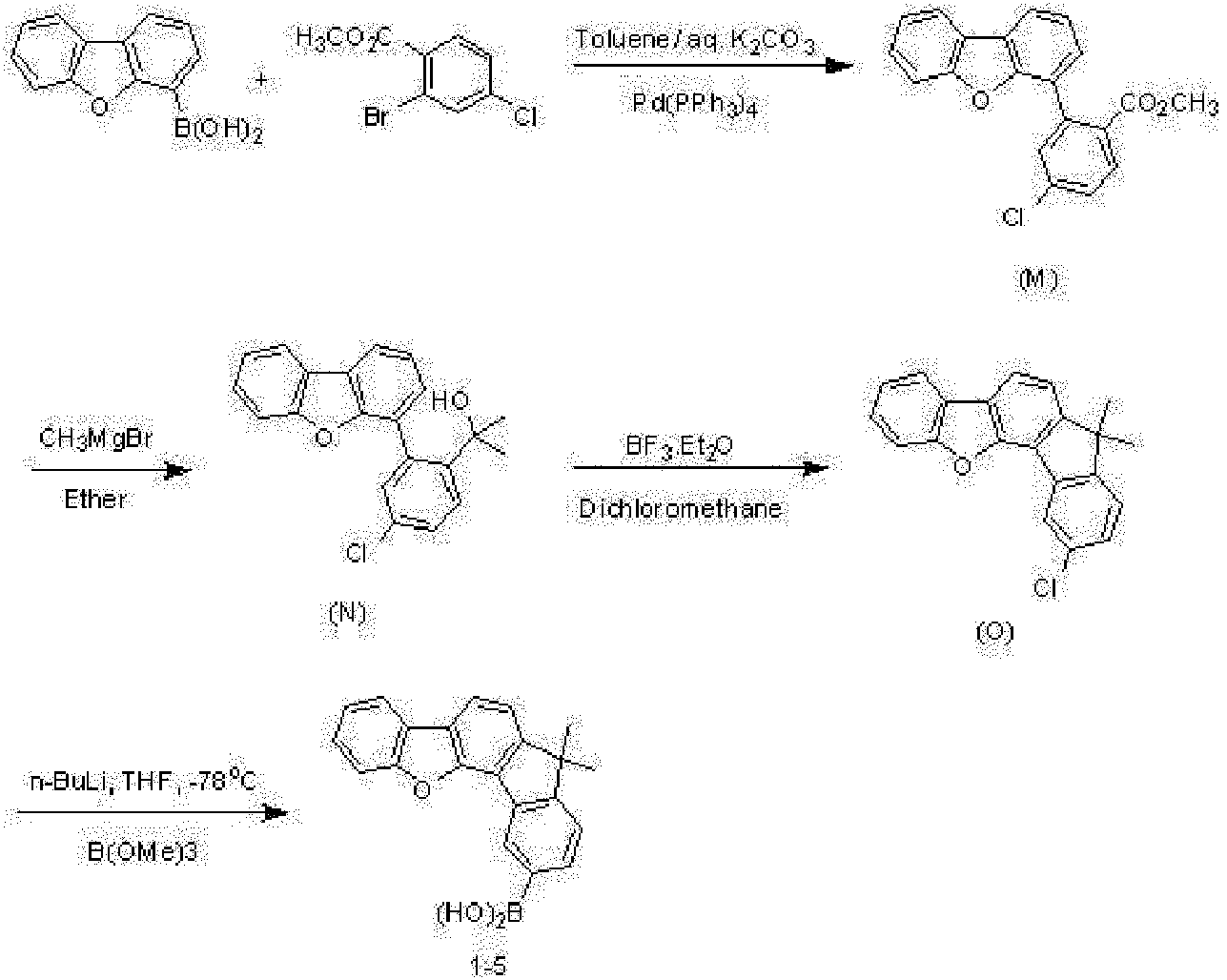
- An intermediate 1-6 was synthesized by using (4-dibenzothienyl)boronic acid as a synthesis starting material through the same steps in Reaction Scheme 6 as the intermediate 1-5.

-

- 10 g (29.1 mmol) of the intermediate 1-2, 10.3 g (26.4 mmol) of the compound B-23, 10.95 g (79.23 mmol) of potassium carbonate, and 0.61 g (0.53 mmmol) of tetrakis-(triphenylphosphine)palladium (0) were suspended in 100 ml of toluene and 40 ml of distilled water and then, refluxed and agitated for 12 hours. The resultant was extracted with dichloromethane and distilled water, and an organic layer was silica gel-filtered. Then, an organic solution was removed therefrom, its residue was silica gel columned with hexane:dichloromethane = 7 : 3 (v/v), and a solid product was recrystallized with dichloromethane and n-hexane, obtaining 14 g (a yield : 87 %) of a compound represented by Chemical Formula 1-F.
- Compounds respectively represented by Chemical Formula 1-A to 1-E and 1-G to 1-P were synthesized in the same method as Example 1 except for using the compounds arranged in Tables 8-1 to 8-3 instead of the intermediate 1-2 and the compound B-23 in Example 1.
[Table 8-1] Ex Starting material 1 Starting material 2 Product Yield (%) LC-Mass (M+H-) 2 


82 % 515.21 3 
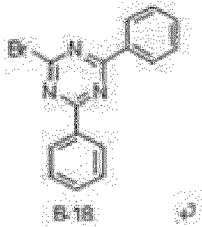

80 % 516.20 4 


78 % 592.23 5 


85 % 531.19 6 


79 % 608.21 7 


88 % 515.21 [Table 8-2] 8 


89 % 516.20 9 


82 % 592.23 10 


88 % 582.18 11 
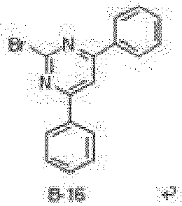

87 % 515.21 12 


85 % 516.20 13 


77 % 591.24 [Table 8-3] 14 


80 % 592.23 15 


84 % 531.19 16 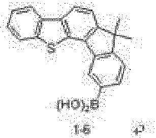


80 % 608.21 -

- 9.97 g (30.95 mmol) of penylcarbazolylbromide, 9.78 g (34.05 mmol) of phenylcarbazolylboronic acid, 12.83 g (92.86 mmol) of potassium carbonate, and 1.07 g (0.93 mmmol) of tetrakis-(triphenylphosphine)palladium (0) were suspended in 120 ml of toluene and 50 ml of distilled water and then, refluxed and agiated for 12 hours. The resultant was extracted with dichloromethane and distilled water, and an organic layer was silica gel-filtered. Then, an organic solution was removed therefrom, and a solid product therefrom was recrystallized with dichloromethane and n-hexane, obtaining 13.8 g (a yield: 92 %) of a compound represented by Chemical Formula 2-A.
- A compound was prepared according to the same method as above except for using two starting materials provided in the following Table instead of Phenylcarbazolylbromide (corresponding to a starting material 1 in Table 9) and phenylcarbazolylboronic acid (corresponding to a starting material 2 in Table 9) of Example 17.
[Table 9] Ex Starting material 1 Starting material 2 Product Yield (%) LC-Mass (H+H+) 18 


90 % 561.23 19 


85 % 637.27 -


- 10 g (34.83 mmol) of phenylcarbazolylboronic acid, 11.77 g (38.31 mmol) of the compound A-8, 14.44 g (104.49 mmol) of potassium carbonate, and 0.80 g (0.7 mmmol) of tetrakis-(triphenylphosphine)palladium (0) were suspended in 140 ml of toluene and 50 ml of distilled water and then, refluxed and agitated for 12 hours. The resultant was extracted with dichloromethane and distilled water, and an organic layer was silica gel-filtered. After removing an organic solution therefrom, its residue was silica gel columned with hexane : dichloromethane = 7 : 3 (v/v), and a solid product therefrom was recrystallized with dichloromethane and n-hexane, obtaining 14.4 g (a yield : 88 %) of a compound represented by Chemical Formula 3-A.
- Each compound respectively represented by Chemical Formulae 3-B to 3-E was synthesized according to the same method as Example 20 except for using compounds arranged in Table 10 instead of the phenylcarbazoleyl boronic acid and the compound A-8 of Example 20.
[Table 10] Ex Starting material 1 Starting material 2 Product Yield(%) LC-Mass (M+H+) 21 


89% 395.14 22 


90 % 411.12 23 


92 % 395.14 24 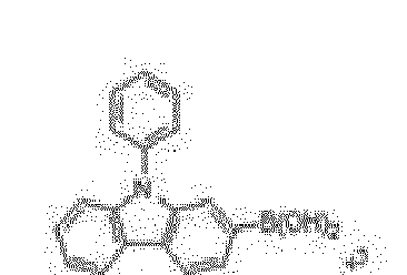


90 % 470.19 - As for an anode, 1000 Å-thick ITO was used, and as for a cathode, 1000 Å-thick aluminum (Al) was used. Specifically, illustrating a method of manufacturing the organic light emitting diode, the anode is manufactured by cutting an ITO glass substrate having 15 Ω/cm2 of sheet resistance into a size of 50 mm × 50 mm × 0.7 mm, ultrasonic wave-cleaning them in acetone, isopropylalcohol, and pure water for 15 minutes respectively, and UV ozone cleaning them for 30 minutes.
- On the substrate, an 800 Å-thick hole transport layer (HTL) was formed by depositing N4,N4'-di(naphthalen-1-yl)-N4,N4'-diphenylbiphenyl-4,4'-diamine (NPB) under a vacuum degree 650×10-7 Pa at a deposit speed of 0.1 to 0.3 nm/s. Subsequently, a 300 Å-thick emission layer was formed through a vacuum depositon by mixing the compound 1-F of Example 1 and the compound 2-A of Example 17 which are obtained under the same vacuum deposit conditio in a weight ratio of 1:1 as a host and simultaneously, doping the mixture with a phosphorescent dopant of Ir(ppy)3. Herein, the phosphorescent dopant was deposited in an amount of 10 wt% based on 100 wt% of the total amount of the emission layer by adjusting its deposit speed.
- On the emission layer, a 50 Å-thick hole blocking layer was formed by depositing bis(2-methyl-8-quinolinolate)-4-(phenylphenolato)aluminium (BAIq) under the same vacuum deposit condition. Subsequently, a 250 Å-thick electron transport layer was formed by depositing Alq3 under the same vacuum deposit condition. On the electron transport layer, a cathode was formed by sequentially depositing LiF and Al, manufacturing an organic photoelectric device.
- The organic photoelectric device had a structure of ITO/ NPB (80 nm)/ EML (compound 1-F (45 wt%) + compound 2-A (45 wt%) + Ir(PPy)3 (10 wt%), 30 nm)/ Balq (5 nm)/ Alq3 (25 nm)/ LiF (1 nm) / Al (100 nm).
- An organic light emitting diode was manufactured according to the same method as Example 25 except for using the compound 1-F and the compound 2-A in a ratio of 4:1 instead of mixing the compound 1-F and the compound 2-A in a weight ratio of 1:1.
- An organic light emitting diode was manufactured according to the same method as Example 25 except for using the compound 1-F and the compound 2-A in a ratio of 1:4 instead of mixing the compound 1-F and the compound 2-A in a weight ratio of 1:1.
- An organic light emitting diode was manufactured according to the same method as Example 25 except for depositing the compound 1-N according to Example 14 and the compound 2-A in a ratio of 1:1 instead of mixing the compound 1-F and the compound 2-A in a weight ratio of 1:1.
- An organic light emitting diode was manufactured according to the same method as Example 28 except for depositing the compound 1-N and the compound 2-A in a ratio of 4:1 instead of mixing the compound 1-N and the compound 2-A in a weight ratio of 1:1.
- An organic light emitting diode was manufactured according to the same method as Example 28 except for depositing the compound 1-N and the compound 2-A in a ratio of 1:4 instead of mixing the compound 1-N and the compound 2-A in a weight ratio of 1:1.
- An organic light emitting diode was manufactured according to the same method as Example 28 except for depositing the compound 1-N and the compound 3-A according to Example 22 in a ratio of 1:1 instead of mixing the compound 1-N and the compound 2-A in a weight ratio of 1:1.
- An organic light emitting diode was manufactured according to the same method as Example 31 except for depositing the compound 1-N and the compound 3-A in a ratio of 4:1 instead of mixing the compound 1-N and the compound 3-A in a weight ratio of 1:1.
- An organic light emitting diode was manufactured according to the same method as Example 31 except for depositing the compound 1-N and the compound 3-A in a ratio of 1:4 instead of mixing the compound 1-N and the compound 3-A in a weight ratio of 1:1.
- An organic light emitting diode was manufactured according to the same method as Example 25 except for depositing the compound 1-F as a single host instead of mixing the compound 1-F and the compound 2-A in a weight ratio of 1:1.
- An organic light emitting diode was manufactured according to the same method as Example 28 except for depositing the compound 1-N as a single host instead of mixing the compound 1-N and the compound 2-A in a weight ratio of 1:1.
- An organic light emitting diode was manufactured according to the same method as Example 28 except for depositing the compound 2-A as a single host instead of mixing the compound 1-N and the compound 2-A in a weight ratio of 1:1.
- An organic light emitting diode was manufactured according to the same method as Example 31 except for depositing the compound 3-A as a host instead of mixing the compound 1-N and the compound 2-A in a weight ratio of 1:1.
- Current density, luminance changes and luminous efficiency depending on a voltage of each organic light emitting diode according to Examples 25 to 33 and Comparative Examples 1 to 4 were measured.
- The measurements were specifically performed in the following method, and the results were provided in Table.
- Current values flowing in the unit device of the manufactured organic light emitting diodes were measured for, while increasing the voltage from 0V to 10V using a current-voltage meter (Keithley 2400), and the measured current values were divided by an area to provide the results.
- Luminance of the manufactured organic light emitting diodes was measured for luminance, while increasing the voltage from 0 V to 10 V using a luminance meter (Minolta Cs-1000A).
- Current efficiency (cd/A) at the same current density (10 mA/cm2) were calculated by using the luminance, current density, and voltages (V) from the items (1) and (2).
- Life-span was obtained by measuring time taken until current efficiency (cd/A) decreased down to 95 % while luminance (cd/m2) was maintained at 5000 cd/m2.
(Table 11) Compound of emission layer Driving voltage (V) Color (EL color) Efficie ncy (cd/A) 95 % life-span (h) @ 5000 cd/m2 Example 25 1-F + 2-A (1:1) 3.96 Green 53.3 300 Example 26 1-F + 2-A (4:1) 3.81 Green 38.2 220 Example 27 1-F + 2-A (1:4) 5.02 Green 39.4 80 Example 28 1-N + 2-A (1:1) 4.26 Green 53.4 240 Example 29 1-N + 2-A (4:1) 4.24 Green 36.9 260 Example 30 1-N + 2-A (1:4) 8.44 Green 25.0 - Example 31 1-N+3-A (1:1) 4.77 Green 38.8 380 Example 32 1-N+3-A (4:1) 4.56 Green 27.8 180 Example 33 1-N+3-A (1:4) 5.66 Green 47.3 200 Comparative Example 1 1-F 4.29 Green 23.6 170 Comparative Example 2 1-N 4.82 Green 21.0 90 Comparative Example 3 2-A 7.13 Green 1.7 - Comparative Example 4 3-A 8.68 Green 16.5 20 - Referring to Table 11, the organic light emitting diodes according to Examples 25 to 33 showed remarkably improved luminous efficiency or/life-span compared with the organic light emitting diodes according to Comparative Examples 1 to 4. Specifically, the organic light emitting diode according to Example 31 showed improved efficiency and superbly improved life-span compared with the organic light emitting diodes according to Comparative Examples 2 and 4. The reason is that the efficiency and the life-span were improved by bipolar characteristics of a hole-transporting host and an electron-transporting host.

- While this invention has been described in connection with what is presently considered to be practical exemplary embodiments, it is to be understood that the invention is not limited to the disclosed embodiments, but, on the contrary, is intended to cover various modifications and equivalent arrangements included within the spirit and scope of the appended claims. Therefore, the aforementioned embodiments should be understood to be exemplary but not limiting the present invention in any way.
Claims (20)
- A composition comprising a first host compound represented by Chemical Formula I and a second host compound represented by Chemical Formula II:

X1 is O, Se, S, SO, SO2, PO, or CO,
X2 is CRaRb or SircRd, and
R1 to R5 and Ra to Rd are each independently hydrogen, deuterium, a substituted or unsubstituted C1 to C30 alkyl group, a substituted or unsubstituted C3 to C30 cycloalkyl group, a substituted or unsubstituted C3 to C30 heterocycloalkyl group, a substituted or unsubstituted C6 to C30 aryl group, a substituted or unsubstituted C3 to C30 heteroaryl group, a substituted or unsubstituted amine group, a substituted or unsubstituted C6 to C30 arylamine group, a substituted or unsubstituted C3 to C30 heteroarylamine group, a substituted or unsubstituted C1 to C30 alkoxy group, a substituted or unsubstituted C2 to C30 alkoxycarbonyl group, a substituted or unsubstituted C2 to C30 alkoxycarbonylamino group, a substituted or unsubstituted C7 to C30 aryloxycarbonylamino group, a substituted or unsubstituted C1 to C30 sulfamoylamino group, a substituted or unsubstituted C2 to C30 alkenyl group, a substituted or unsubstituted C2 to C30 alkynyl group, a substituted or unsubstituted silyl group, a substituted or unsubstituted silyloxy group, a substituted or unsubstituted C1 to C30 acyl group, a substituted or unsubstituted C1 to C20 acyloxy group, a substituted or unsubstituted C1 to C20 acylamino group, a substituted or unsubstituted C1 to C30 sulfonyl group, a substituted or unsubstituted C1 to C30 alkylthiol group, a substituted or unsubstituted C1 to C30 heterocyclothiol group, a substituted or unsubstituted C6 to C30 arylthiol group, a substituted or unsubstituted C1 to C30 heteroarylthiol group, a substituted or unsubstituted C1 to C30 ureide group, a halogen, a halogen-containing group, a cyano group, a hydroxyl group, an amino group, a nitro group, a carboxyl group, a ferrocenyl group, or a combination thereof,
X3 is O, S, CRuRv, SiRwRx, or NRy,
HTU is a substituted or unsubstituted carbazolyl group or a substituted or unsubstituted triphenylenyl group, and
R11 to R13 and Ru to Ry are each independently hydrogen, deuterium, a substituted or unsubstituted C1 to C20 alkyl group, a substituted or unsubstituted C6 to C30 aryl group, a substituted or unsubstituted C3 to C30 heteroaryl group, or a combination thereof. - The composition of claim 1, wherein the first host compound is represented by one of Chemical Formulae 1 a to 1 c:
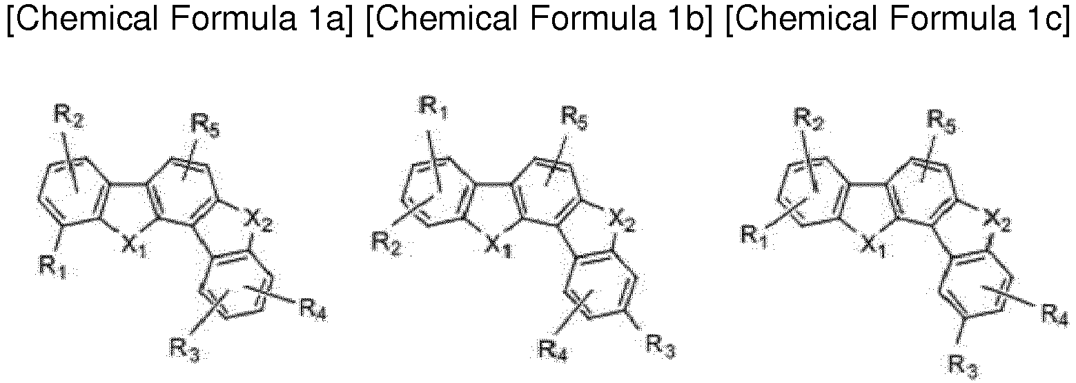
X1 is O, Se, S, SO, SO2, PO, or CO,
X2 is CRaRb or SiRcRd, and
R1 to R5 and Ra to Rd are each independently hydrogen, deuterium, a substituted or unsubstituted C1 to C30 alkyl group, a substituted or unsubstituted C3 to C30 cycloalkyl group, a substituted or unsubstituted C3 to C30 heterocycloalkyl group, a substituted or unsubstituted C6 to C30 aryl group, a substituted or unsubstituted C3 to C30 heteroaryl group, a substituted or unsubstituted amine group, a substituted or unsubstituted C6 to C30 arylamine group, a substituted or unsubstituted C3 to C30 heteroarylamine group, a substituted or unsubstituted C1 to C30 alkoxy group, a substituted or unsubstituted C2 to C30 alkoxycarbonyl group, a substituted or unsubstituted C2 to C30 alkoxycarbonylamino group, a substituted or unsubstituted C7 to C30 aryloxycarbonylamino group, a substituted or unsubstituted C1 to C30 sulfamoylamino group, a substituted or unsubstituted C2 to C30 alkenyl group, a substituted or unsubstituted C2 to C30 alkynyl group, a substituted or unsubstituted silyl group, a substituted or unsubstituted silyloxy group, a substituted or unsubstituted C1 to C30 acyl group, a substituted or unsubstituted C1 to C20 acyloxy group, a substituted or unsubstituted C1 to C20 acylamino group, a substituted or unsubstituted C1 to C30 sulfonyl group, a substituted or unsubstituted C1 to C30 alkylthiol group, a substituted or unsubstituted C1 to C30 heterocyclothiol group, a substituted or unsubstituted C6 to C30 arylthiol group, a substituted or unsubstituted C1 to C30 heteroarylthiol group, a substituted or unsubstituted C1 to C30 ureide group, a halogen, a halogen-containing group, a cyano group, a hydroxyl group, an amino group, a nitro group, a carboxyl group, a ferrocenyl group or a combination thereof. - The composition of claim 1, wherein the first host compound is represented by one of Chemical Formulae 1-1 to 1-6:


R1 to R5 are each independently hydrogen, deuterium, a substituted or unsubstituted C1 to C20 alkyl group, a substituted or unsubstituted C6 to C30 aryl group, a substituted or unsubstituted C3 to C30 heteroaryl group, or a combination thereof. - The composition of claim 1, wherein at least one of R1 to R5 and Ra to Rd is selected from substituted or unsubstituted functional groups of Group 1:

Y is N, O, S, SO2, NRj, CRk, SiRl, CRmRn or SiRoRp,
Z is N, CRq, CRrRs or NRt,
wherein Rj to Rt are each independently hydrogen, deuterium, a substituted or unsubstituted C1 to C20 alkyl group, a substituted or unsubstituted C6 to C30 aryl group, a substituted or unsubstituted C3 to C30 heteroaryl group, or a combination thereof,
Ar5 is a single bond, a substituted or unsubstituted C1 to C20 alkylene group, a substituted or unsubstituted C2 to C20 alkenylene group, a substituted or unsubstituted C6 to C30 arylene group, a substituted or unsubstituted C2 to C30 heteroarylene group, a substituted or unsubstituted C6 to C30 arylamine group, a substituted or unsubstituted C2 to C30 heteroarylamine group, or a combination thereof,
Ar6 and Ar7 are independently substituted or unsubstituted C6 to C30 aryl group, a substituted or unsubstituted C3 to C30 heteroaryl group, or a combination thereof,
n1 and n2 are each independently 0 or 1, and
* is a linking point to Chemical Formula 1 and may be positioned at one of elements of the functional group. - The composition of claim 4, wherein the substituted or unsubstituted functional group of Group 1 is selected from substituted or unsubstituted Chemical Formulae B-1 to B-35:


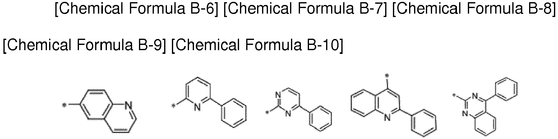


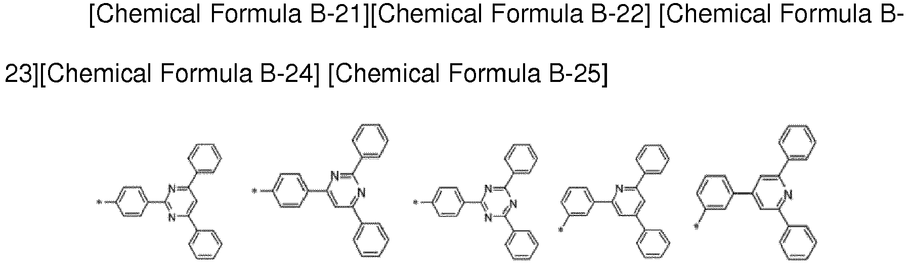

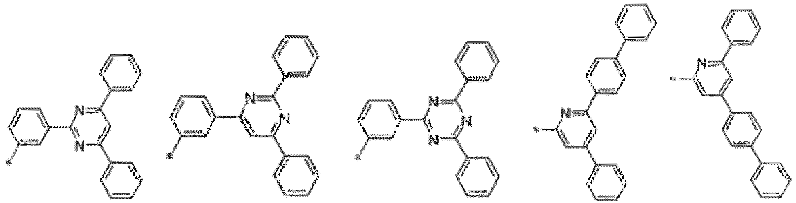
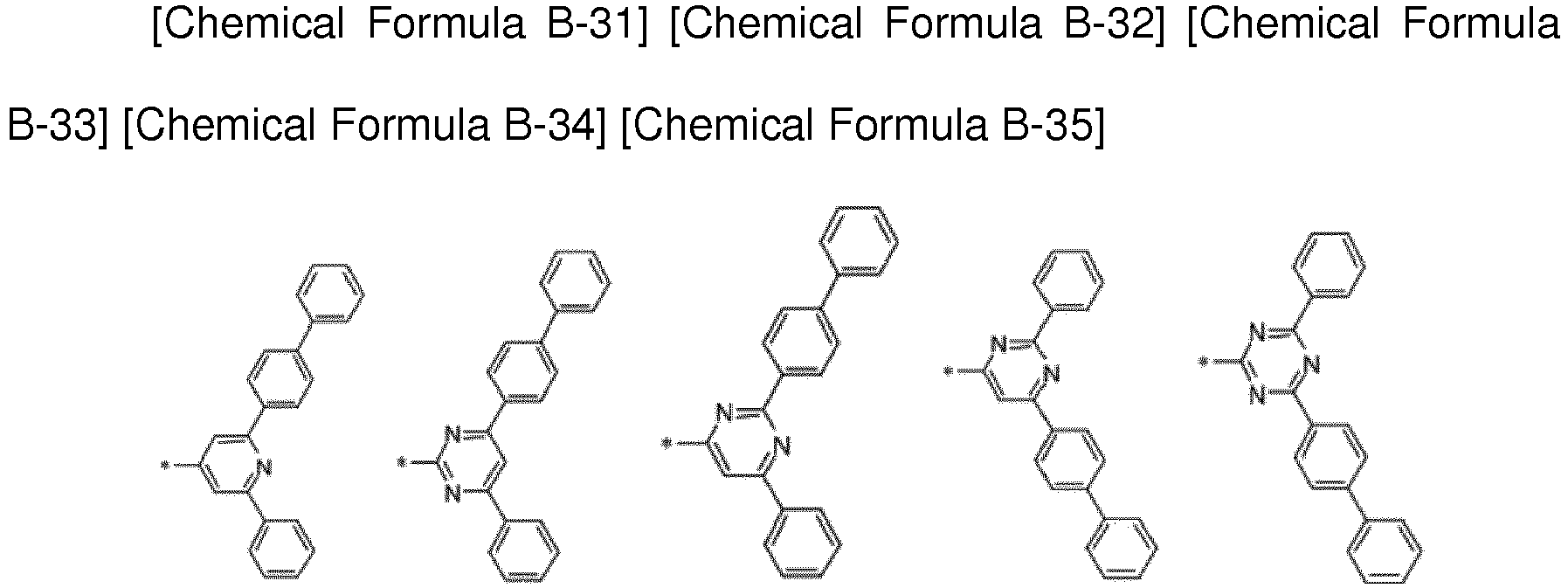
- The composition of claim 1, wherein the first host compound is selected from Chemical Formulae 1-A to 1-P:


- The composition of claim 1, wherein the second host compound is represented by Chemical Formula 2:

Ar1, Ar2 and R11 to R16 are each independently hydrogen, deuterium, a substituted or unsubstituted C1 to C20 alkyl group, a substituted or unsubstituted C6 to C30 aryl group, a substituted or unsubstituted C3 to C30 heteroaryl group, or a combination thereof. - The composition of claim 7, wherein the second host compound is represetnted by one of Chemical Formulae 2-1 to 2-3:

Ar1, Ar2 and R11 to R16 are each independently hydrogen, deuterium, a substituted or unsubstituted C1 to C20 alkyl group, a substituted or unsubstituted C6 to C30 aryl group, a substituted or unsubstituted C3 to C30 heteroaryl group, or a combination thereof. - The composition of claim 7, wherein Ar1 and Ar2 of Chemical Formula 2 are each independently selected from substituted or unsubstituted Chemical Formulae A-1 to A-15:


- The composition of claim 7, wherein the second host compound is represented by Chemical Formulae 2-A to 2-C:

- The composition of claim 1, wherein the second host compound is represented by Chemical Formula 3:


X3 is O, S, CReRf, SiRgRh or NRi,
L is a single bond, a substituted or unsubstituted C1 to C20 alkylene group, a substituted or unsubstituted C2 to C20 alkenylene group, a substituted or unsubstituted C6 to C30 arylene group, a substituted or unsubstituted C2 to C30 heteroarylene group, or a combination thereof, and
R11 to R13, R17 to R21, and Re to Ri are each independently hydrogen, deuterium, a substituted or unsubstituted C1 to C20 alkyl group, a substituted or unsubstituted C6 to C30 aryl group, a substituted or unsubstituted C3 to C30 heteroaryl group, or a combination thereof. - The composition of claim 11, wherein the second host compound is represented by Chemical Formula 3a:

X3 is O, S, CReRf, SiRgRh, or NRi,
L is a single bond, a substituted or unsubstituted C1 to C20 alkylene group, a substituted or unsubstituted C2 to C20 alkenylene group, a substituted or unsubstituted C6 to C30 arylene group, a substituted or unsubstituted C2 to C30 heteroarylene group, or a combination thereof, and
R11 to R13, R17 to R21, and Re to Ri are each independently hydrogen, deuterium, a substituted or unsubstituted C1 to C20 alkyl group, a substituted or unsubstituted C6 to C30 aryl group, a substituted or unsubstituted C3 to C30 heteroaryl group, or a combination thereof. - The composition of claim 11, wherein the second host compound is represented by one of Chemical Formulae 3-1 to 3-10:


R11 to R13, R17 to R21, and Ri are each independently hydrogen, deuterium, a substituted or unsubstituted C1 to C20 alkyl group, a substituted or unsubstituted C6 to C30 aryl group, a substituted or unsubstituted C3 to C30 heteroaryl group, or a combination thereof. - The composition of claim 11, wherein at least one of R11 to R13, R17 to R21, and Re to Ri is selected from substituted or unsubstituted Chemical Formulae A-1 to A-15.


- The composition of claim 11, wherein the second host compound is represented by one of Chemical Formulae 3-A to 3-E:


- The composition of claim 1, wherein the first host compound and the second host compound are included in a weight ratio of 1:10 to 10:1.
- The composition of claim 1, further comprising a phosphorescent dopant.
- An organic optoelectric device comprising
an anode and a cathode facing each other, and
at least one organic layer interposed between the anode and the cathode,
wherein the organic layer comprises the composition of any one of claim 1 to claim 16. - The organic optoelectric device of claim 18, wherein the organic layer comprises an emission layer, and
the emission layer comprises the composition - A display device comprising the organic optoelectric device of claim 18.
Applications Claiming Priority (2)
| Application Number | Priority Date | Filing Date | Title |
|---|---|---|---|
| KR1020130095619A KR101686078B1 (en) | 2013-08-12 | 2013-08-12 | Composition and organic optoelectric device and display device |
| PCT/KR2014/001390 WO2015023034A1 (en) | 2013-08-12 | 2014-02-20 | Composition, organic optoelectronic element, and display device |
Publications (3)
| Publication Number | Publication Date |
|---|---|
| EP3034581A1 true EP3034581A1 (en) | 2016-06-22 |
| EP3034581A4 EP3034581A4 (en) | 2017-03-29 |
| EP3034581B1 EP3034581B1 (en) | 2018-04-04 |
Family
ID=52468409
Family Applications (1)
| Application Number | Title | Priority Date | Filing Date |
|---|---|---|---|
| EP14836457.3A Active EP3034581B1 (en) | 2013-08-12 | 2014-02-20 | Composition and organic optoelectronic element |
Country Status (6)
| Country | Link |
|---|---|
| US (1) | US20160133851A1 (en) |
| EP (1) | EP3034581B1 (en) |
| JP (1) | JP6409065B2 (en) |
| KR (1) | KR101686078B1 (en) |
| CN (1) | CN105473684A (en) |
| WO (1) | WO2015023034A1 (en) |
Cited By (3)
| Publication number | Priority date | Publication date | Assignee | Title |
|---|---|---|---|---|
| WO2024177457A1 (en) | 2023-02-23 | 2024-08-29 | 삼성에스디아이 주식회사 | Compound for organic optoelectronic device, composition for organic optoelectronic device, organic optoelectronic device, and display device |
| WO2024177455A1 (en) | 2023-02-23 | 2024-08-29 | 삼성에스디아이 주식회사 | Compound for organic optoelectronic device, composition for organic optoelectronic device, organic optoelectronic device and display device |
| US12501829B2 (en) | 2020-11-04 | 2025-12-16 | Samsung Sdi Co., Ltd. | Compound for organic optoelectronic device, composition for organic optoelectronic device, organic optoelectronic device, and display device |
Families Citing this family (16)
| Publication number | Priority date | Publication date | Assignee | Title |
|---|---|---|---|---|
| KR102292768B1 (en) * | 2015-10-13 | 2021-08-25 | 롬엔드하스전자재료코리아유한회사 | Organic Electroluminescent Compounds and Organic Electroluminescent Devices Comprising the Same |
| CN108349923A (en) * | 2015-11-13 | 2018-07-31 | Sfc株式会社 | Novel heterocyclic compounds and organic illuminating element including this |
| KR101928934B1 (en) * | 2016-02-23 | 2018-12-13 | 주식회사 엘지화학 | Hetero-cyclic compound and organic light emitting device comprising the same |
| KR102054276B1 (en) | 2016-06-29 | 2019-12-10 | 삼성에스디아이 주식회사 | Compound for organic optoelectronic device, composition for organic optoelectronic device and organic optoelectronic device and display device |
| KR102027961B1 (en) | 2016-06-29 | 2019-10-02 | 삼성에스디아이 주식회사 | Compound for organic optoelectronic device, composition for organic optoelectronic device and organic optoelectronic device and display device |
| KR102050000B1 (en) | 2016-07-12 | 2019-11-28 | 삼성에스디아이 주식회사 | Compound for organic optoelectronic device, composition for organic optoelectronic device and organic optoelectronic device and display device |
| KR102049419B1 (en) * | 2016-07-19 | 2019-11-27 | 삼성에스디아이 주식회사 | Composition for organic optoelectronic device and organic optoelectronic device and display device |
| KR102054277B1 (en) * | 2016-07-29 | 2019-12-10 | 삼성에스디아이 주식회사 | Composition for organic optoelectronic device and organic optoelectronic device and display device |
| US11158817B2 (en) | 2017-01-05 | 2021-10-26 | Samsung Sdi Co., Ltd. | Compound for organic optoelectronic device, composition for organic optoelectronic device and organic optoelectronic device and display device |
| KR102506419B1 (en) * | 2017-07-13 | 2023-03-07 | 솔루스첨단소재 주식회사 | Organic compound and organic electroluminescent device comprising the same |
| KR102146792B1 (en) | 2017-08-01 | 2020-08-21 | 삼성에스디아이 주식회사 | Compound for organic optoelectronic device, and organic optoelectronic device and display device |
| CN108047235B (en) * | 2017-12-29 | 2019-10-18 | 西安瑞联新材料股份有限公司 | A kind of aromatic heterocyclic compounds and its application |
| KR102599003B1 (en) * | 2020-04-20 | 2023-11-03 | 삼성에스디아이 주식회사 | Composition for organic optoelectronic device, organic optoelectronic device and display device |
| KR102761654B1 (en) * | 2020-04-21 | 2025-01-31 | 삼성에스디아이 주식회사 | Compound for organic optoelectronic device, composition for organic optoelectronic device, organic optoelectronic device and display device |
| KR102832336B1 (en) * | 2021-05-10 | 2025-07-14 | 엘티소재주식회사 | Condensed multicyclic compound and organic light emitting device including same |
| CN115594705B (en) * | 2021-07-07 | 2025-03-25 | 三星Sdi株式会社 | Compound for organic photoelectric device, composition for organic photoelectric device, organic photoelectric device and display device |
Family Cites Families (17)
| Publication number | Priority date | Publication date | Assignee | Title |
|---|---|---|---|---|
| KR20160086983A (en) * | 2007-08-08 | 2016-07-20 | 유니버셜 디스플레이 코포레이션 | Benzo-fused thiophene or benzo-fused furan compounds comprising a triphenylene group |
| US8221905B2 (en) * | 2007-12-28 | 2012-07-17 | Universal Display Corporation | Carbazole-containing materials in phosphorescent light emitting diodes |
| DE102009005288A1 (en) * | 2009-01-20 | 2010-07-22 | Merck Patent Gmbh | Materials for organic electroluminescent devices |
| EP2403028B1 (en) * | 2009-02-27 | 2014-11-12 | Nippon Steel & Sumikin Chemical Co., Ltd. | Organic electroluminescent element |
| KR101212670B1 (en) * | 2009-11-03 | 2012-12-14 | 제일모직주식회사 | Composition for organic photoelectric device, organic photoelectric device using the same and display device comprising the same |
| US8227801B2 (en) * | 2010-04-26 | 2012-07-24 | Universal Display Corporation | Bicarbzole containing compounds for OLEDs |
| JP2012028634A (en) * | 2010-07-26 | 2012-02-09 | Idemitsu Kosan Co Ltd | Organic electroluminescent element |
| US9954180B2 (en) * | 2010-08-20 | 2018-04-24 | Universal Display Corporation | Bicarbazole compounds for OLEDs |
| KR101423173B1 (en) * | 2010-11-04 | 2014-07-25 | 제일모직 주식회사 | Compound for organic photoelectric device and organic photoelectric device including the same |
| KR101531612B1 (en) * | 2010-12-02 | 2015-06-25 | 제일모직 주식회사 | Compound for organic photoelectric device and organic photoelectric device including the same |
| KR101486561B1 (en) * | 2010-12-31 | 2015-01-26 | 제일모직 주식회사 | Compound for organic photoelectric device and organic photoelectric device including the same |
| WO2012111680A1 (en) * | 2011-02-16 | 2012-08-23 | Semiconductor Energy Laboratory Co., Ltd. | Light-emitting body, light-emitting layer, and light-emitting device |
| JP6197265B2 (en) * | 2011-03-28 | 2017-09-20 | 東レ株式会社 | Light emitting device material and light emitting device |
| WO2012153725A1 (en) * | 2011-05-12 | 2012-11-15 | 東レ株式会社 | Light-emitting element material and light-emitting element |
| KR101497124B1 (en) * | 2011-11-28 | 2015-03-06 | 덕산네오룩스 주식회사 | Compound for organic electronic element, organic electronic element using the same, and an electronic device thereof |
| KR101497133B1 (en) * | 2011-12-23 | 2015-02-27 | 제일모직 주식회사 | Compound for organic OPTOELECTRONIC device, ORGANIC LIGHT EMITTING DIODE INCLUDING THE SAME and DISPLAY INCLUDING THE organic LIGHT EMITTING DIODE |
| KR20130084093A (en) * | 2012-01-16 | 2013-07-24 | 롬엔드하스전자재료코리아유한회사 | Novel organic electroluminescence compounds and organic electroluminescence device using the same |
-
2013
- 2013-08-12 KR KR1020130095619A patent/KR101686078B1/en active Active
-
2014
- 2014-02-20 JP JP2016533229A patent/JP6409065B2/en active Active
- 2014-02-20 WO PCT/KR2014/001390 patent/WO2015023034A1/en not_active Ceased
- 2014-02-20 CN CN201480044784.6A patent/CN105473684A/en active Pending
- 2014-02-20 EP EP14836457.3A patent/EP3034581B1/en active Active
- 2014-02-20 US US14/896,547 patent/US20160133851A1/en not_active Abandoned
Cited By (5)
| Publication number | Priority date | Publication date | Assignee | Title |
|---|---|---|---|---|
| US12501829B2 (en) | 2020-11-04 | 2025-12-16 | Samsung Sdi Co., Ltd. | Compound for organic optoelectronic device, composition for organic optoelectronic device, organic optoelectronic device, and display device |
| WO2024177457A1 (en) | 2023-02-23 | 2024-08-29 | 삼성에스디아이 주식회사 | Compound for organic optoelectronic device, composition for organic optoelectronic device, organic optoelectronic device, and display device |
| WO2024177455A1 (en) | 2023-02-23 | 2024-08-29 | 삼성에스디아이 주식회사 | Compound for organic optoelectronic device, composition for organic optoelectronic device, organic optoelectronic device and display device |
| EP4672948A1 (en) | 2023-02-23 | 2025-12-31 | Samsung Sdi Co., Ltd. | Connection for organic optoelectronic device, assembly for organic optoelectronic device, organic optoelectronic device and display device |
| EP4672947A1 (en) | 2023-02-23 | 2025-12-31 | Samsung Sdi Co., Ltd. | Connection for organic optoelectronic device, assembly for organic optoelectronic device, organic optoelectronic device and display device |
Also Published As
| Publication number | Publication date |
|---|---|
| CN105473684A (en) | 2016-04-06 |
| WO2015023034A1 (en) | 2015-02-19 |
| KR20150019154A (en) | 2015-02-25 |
| US20160133851A1 (en) | 2016-05-12 |
| JP2016534555A (en) | 2016-11-04 |
| JP6409065B2 (en) | 2018-10-17 |
| EP3034581A4 (en) | 2017-03-29 |
| KR101686078B1 (en) | 2016-12-13 |
| EP3034581B1 (en) | 2018-04-04 |
Similar Documents
| Publication | Publication Date | Title |
|---|---|---|
| EP3034581B1 (en) | Composition and organic optoelectronic element | |
| EP3575296B1 (en) | Triazine compound, composition and organic optoelectronic device and display device | |
| EP3901148B1 (en) | Compound for organic optoelectronic element, composition for organic optoelectronic element and organic optoelectronic element and display device | |
| EP3492553B1 (en) | Composition for organic optoelectronic element, organic optoelectronic element, and display device | |
| EP3032606B1 (en) | Organic optoelectric device and display device | |
| EP2860783B1 (en) | Organic optoelectric device and display device | |
| EP3042943B1 (en) | Composition for organic optoelectronic device, organic optoelectronic device, and display device | |
| EP2952511B1 (en) | Organic compound, organic optoelectronic device and display device | |
| EP3486299B1 (en) | Compound for organic optoelectronic device, composition for organic optoelectronic device, organic optoelectronic device, and display device | |
| EP3168221B1 (en) | Compound, organic optoelectronic diode comprising same, and display | |
| TWI641607B (en) | Compound for organic optoelectric device, composition for organic optoelectric device, and organic optoelectric device and display device | |
| EP2998300A1 (en) | Organic compound, organic optoelectronic element, and display device | |
| EP3530653A1 (en) | Organic compound, organic optoelectronic element, and display device | |
| EP4458822A1 (en) | Compound for organic optoelectronic device, composition for organic optoelectronic device, organic optoelectronic device, and display device | |
| EP4369901A2 (en) | Composition for organic optoelectronic diode, organic optoelectronic diode, and display device | |
| KR20160012028A (en) | Condensed cyclic compound and organic light emitting device including the same | |
| KR20160019747A (en) | Compound, organic optoelectric device and display device | |
| EP3992190A1 (en) | Compound for organic optoelectronic diode, composition for organic optoelectronic diode, organic optoelectronic diode, and display device | |
| EP2876104A1 (en) | Polycyclic compound and organic electronic device comprising same | |
| KR101627743B1 (en) | Compound, light emitting diode, organic optoelectric device, and display device | |
| EP3023425B1 (en) | Compound, organic optoelectronic element comprising same, and display device | |
| CN112592333B (en) | Compound for organic photoelectric device, organic photoelectric device and display device | |
| EP3660012B1 (en) | Compound for organic optoelectronic device and organic optoelectronic device and display device | |
| CN107880045A (en) | Compound for organic photoelectric device, the composition for organic photoelectric device and organic photoelectric device and display device | |
| KR101648141B1 (en) | Compound, organic optoelectric device, and display device |
Legal Events
| Date | Code | Title | Description |
|---|---|---|---|
| PUAI | Public reference made under article 153(3) epc to a published international application that has entered the european phase |
Free format text: ORIGINAL CODE: 0009012 |
|
| 17P | Request for examination filed |
Effective date: 20160127 |
|
| AK | Designated contracting states |
Kind code of ref document: A1 Designated state(s): AL AT BE BG CH CY CZ DE DK EE ES FI FR GB GR HR HU IE IS IT LI LT LU LV MC MK MT NL NO PL PT RO RS SE SI SK SM TR |
|
| AX | Request for extension of the european patent |
Extension state: BA ME |
|
| DAX | Request for extension of the european patent (deleted) | ||
| A4 | Supplementary search report drawn up and despatched |
Effective date: 20170224 |
|
| RIC1 | Information provided on ipc code assigned before grant |
Ipc: C07D 409/04 20060101ALI20170220BHEP Ipc: C09K 11/06 20060101ALI20170220BHEP Ipc: H01L 51/50 20060101AFI20170220BHEP Ipc: C07D 405/04 20060101ALI20170220BHEP |
|
| REG | Reference to a national code |
Ref country code: DE Ref legal event code: R079 Ref document number: 602014023497 Country of ref document: DE Free format text: PREVIOUS MAIN CLASS: C09K0011060000 Ipc: H01L0051540000 |
|
| GRAP | Despatch of communication of intention to grant a patent |
Free format text: ORIGINAL CODE: EPIDOSNIGR1 |
|
| STAA | Information on the status of an ep patent application or granted ep patent |
Free format text: STATUS: GRANT OF PATENT IS INTENDED |
|
| RIC1 | Information provided on ipc code assigned before grant |
Ipc: C07D 405/04 20060101ALI20170928BHEP Ipc: H01L 51/54 20060101AFI20170928BHEP Ipc: C09K 11/06 20060101ALI20170928BHEP Ipc: C07D 409/04 20060101ALI20170928BHEP |
|
| INTG | Intention to grant announced |
Effective date: 20171017 |
|
| GRAS | Grant fee paid |
Free format text: ORIGINAL CODE: EPIDOSNIGR3 |
|
| GRAA | (expected) grant |
Free format text: ORIGINAL CODE: 0009210 |
|
| STAA | Information on the status of an ep patent application or granted ep patent |
Free format text: STATUS: THE PATENT HAS BEEN GRANTED |
|
| AK | Designated contracting states |
Kind code of ref document: B1 Designated state(s): AL AT BE BG CH CY CZ DE DK EE ES FI FR GB GR HR HU IE IS IT LI LT LU LV MC MK MT NL NO PL PT RO RS SE SI SK SM TR |
|
| REG | Reference to a national code |
Ref country code: GB Ref legal event code: FG4D |
|
| REG | Reference to a national code |
Ref country code: CH Ref legal event code: EP |
|
| REG | Reference to a national code |
Ref country code: AT Ref legal event code: REF Ref document number: 986507 Country of ref document: AT Kind code of ref document: T Effective date: 20180415 |
|
| REG | Reference to a national code |
Ref country code: IE Ref legal event code: FG4D |
|
| REG | Reference to a national code |
Ref country code: DE Ref legal event code: R096 Ref document number: 602014023497 Country of ref document: DE |
|
| REG | Reference to a national code |
Ref country code: NL Ref legal event code: MP Effective date: 20180404 |
|
| REG | Reference to a national code |
Ref country code: LT Ref legal event code: MG4D |
|
| PG25 | Lapsed in a contracting state [announced via postgrant information from national office to epo] |
Ref country code: NL Free format text: LAPSE BECAUSE OF FAILURE TO SUBMIT A TRANSLATION OF THE DESCRIPTION OR TO PAY THE FEE WITHIN THE PRESCRIBED TIME-LIMIT Effective date: 20180404 |
|
| PG25 | Lapsed in a contracting state [announced via postgrant information from national office to epo] |
Ref country code: AL Free format text: LAPSE BECAUSE OF FAILURE TO SUBMIT A TRANSLATION OF THE DESCRIPTION OR TO PAY THE FEE WITHIN THE PRESCRIBED TIME-LIMIT Effective date: 20180404 Ref country code: BG Free format text: LAPSE BECAUSE OF FAILURE TO SUBMIT A TRANSLATION OF THE DESCRIPTION OR TO PAY THE FEE WITHIN THE PRESCRIBED TIME-LIMIT Effective date: 20180704 Ref country code: SE Free format text: LAPSE BECAUSE OF FAILURE TO SUBMIT A TRANSLATION OF THE DESCRIPTION OR TO PAY THE FEE WITHIN THE PRESCRIBED TIME-LIMIT Effective date: 20180404 Ref country code: FI Free format text: LAPSE BECAUSE OF FAILURE TO SUBMIT A TRANSLATION OF THE DESCRIPTION OR TO PAY THE FEE WITHIN THE PRESCRIBED TIME-LIMIT Effective date: 20180404 Ref country code: PL Free format text: LAPSE BECAUSE OF FAILURE TO SUBMIT A TRANSLATION OF THE DESCRIPTION OR TO PAY THE FEE WITHIN THE PRESCRIBED TIME-LIMIT Effective date: 20180404 Ref country code: NO Free format text: LAPSE BECAUSE OF FAILURE TO SUBMIT A TRANSLATION OF THE DESCRIPTION OR TO PAY THE FEE WITHIN THE PRESCRIBED TIME-LIMIT Effective date: 20180704 Ref country code: LT Free format text: LAPSE BECAUSE OF FAILURE TO SUBMIT A TRANSLATION OF THE DESCRIPTION OR TO PAY THE FEE WITHIN THE PRESCRIBED TIME-LIMIT Effective date: 20180404 Ref country code: ES Free format text: LAPSE BECAUSE OF FAILURE TO SUBMIT A TRANSLATION OF THE DESCRIPTION OR TO PAY THE FEE WITHIN THE PRESCRIBED TIME-LIMIT Effective date: 20180404 |
|
| PG25 | Lapsed in a contracting state [announced via postgrant information from national office to epo] |
Ref country code: GR Free format text: LAPSE BECAUSE OF FAILURE TO SUBMIT A TRANSLATION OF THE DESCRIPTION OR TO PAY THE FEE WITHIN THE PRESCRIBED TIME-LIMIT Effective date: 20180705 Ref country code: HR Free format text: LAPSE BECAUSE OF FAILURE TO SUBMIT A TRANSLATION OF THE DESCRIPTION OR TO PAY THE FEE WITHIN THE PRESCRIBED TIME-LIMIT Effective date: 20180404 Ref country code: LV Free format text: LAPSE BECAUSE OF FAILURE TO SUBMIT A TRANSLATION OF THE DESCRIPTION OR TO PAY THE FEE WITHIN THE PRESCRIBED TIME-LIMIT Effective date: 20180404 Ref country code: RS Free format text: LAPSE BECAUSE OF FAILURE TO SUBMIT A TRANSLATION OF THE DESCRIPTION OR TO PAY THE FEE WITHIN THE PRESCRIBED TIME-LIMIT Effective date: 20180404 |
|
| REG | Reference to a national code |
Ref country code: AT Ref legal event code: MK05 Ref document number: 986507 Country of ref document: AT Kind code of ref document: T Effective date: 20180404 |
|
| PG25 | Lapsed in a contracting state [announced via postgrant information from national office to epo] |
Ref country code: PT Free format text: LAPSE BECAUSE OF FAILURE TO SUBMIT A TRANSLATION OF THE DESCRIPTION OR TO PAY THE FEE WITHIN THE PRESCRIBED TIME-LIMIT Effective date: 20180806 |
|
| REG | Reference to a national code |
Ref country code: DE Ref legal event code: R097 Ref document number: 602014023497 Country of ref document: DE |
|
| PG25 | Lapsed in a contracting state [announced via postgrant information from national office to epo] |
Ref country code: RO Free format text: LAPSE BECAUSE OF FAILURE TO SUBMIT A TRANSLATION OF THE DESCRIPTION OR TO PAY THE FEE WITHIN THE PRESCRIBED TIME-LIMIT Effective date: 20180404 Ref country code: EE Free format text: LAPSE BECAUSE OF FAILURE TO SUBMIT A TRANSLATION OF THE DESCRIPTION OR TO PAY THE FEE WITHIN THE PRESCRIBED TIME-LIMIT Effective date: 20180404 Ref country code: CZ Free format text: LAPSE BECAUSE OF FAILURE TO SUBMIT A TRANSLATION OF THE DESCRIPTION OR TO PAY THE FEE WITHIN THE PRESCRIBED TIME-LIMIT Effective date: 20180404 Ref country code: AT Free format text: LAPSE BECAUSE OF FAILURE TO SUBMIT A TRANSLATION OF THE DESCRIPTION OR TO PAY THE FEE WITHIN THE PRESCRIBED TIME-LIMIT Effective date: 20180404 Ref country code: DK Free format text: LAPSE BECAUSE OF FAILURE TO SUBMIT A TRANSLATION OF THE DESCRIPTION OR TO PAY THE FEE WITHIN THE PRESCRIBED TIME-LIMIT Effective date: 20180404 Ref country code: SK Free format text: LAPSE BECAUSE OF FAILURE TO SUBMIT A TRANSLATION OF THE DESCRIPTION OR TO PAY THE FEE WITHIN THE PRESCRIBED TIME-LIMIT Effective date: 20180404 |
|
| PLBE | No opposition filed within time limit |
Free format text: ORIGINAL CODE: 0009261 |
|
| STAA | Information on the status of an ep patent application or granted ep patent |
Free format text: STATUS: NO OPPOSITION FILED WITHIN TIME LIMIT |
|
| PG25 | Lapsed in a contracting state [announced via postgrant information from national office to epo] |
Ref country code: SM Free format text: LAPSE BECAUSE OF FAILURE TO SUBMIT A TRANSLATION OF THE DESCRIPTION OR TO PAY THE FEE WITHIN THE PRESCRIBED TIME-LIMIT Effective date: 20180404 Ref country code: IT Free format text: LAPSE BECAUSE OF FAILURE TO SUBMIT A TRANSLATION OF THE DESCRIPTION OR TO PAY THE FEE WITHIN THE PRESCRIBED TIME-LIMIT Effective date: 20180404 |
|
| 26N | No opposition filed |
Effective date: 20190107 |
|
| PG25 | Lapsed in a contracting state [announced via postgrant information from national office to epo] |
Ref country code: SI Free format text: LAPSE BECAUSE OF FAILURE TO SUBMIT A TRANSLATION OF THE DESCRIPTION OR TO PAY THE FEE WITHIN THE PRESCRIBED TIME-LIMIT Effective date: 20180404 |
|
| REG | Reference to a national code |
Ref country code: CH Ref legal event code: PL |
|
| GBPC | Gb: european patent ceased through non-payment of renewal fee |
Effective date: 20190220 |
|
| PG25 | Lapsed in a contracting state [announced via postgrant information from national office to epo] |
Ref country code: MC Free format text: LAPSE BECAUSE OF FAILURE TO SUBMIT A TRANSLATION OF THE DESCRIPTION OR TO PAY THE FEE WITHIN THE PRESCRIBED TIME-LIMIT Effective date: 20180404 Ref country code: LU Free format text: LAPSE BECAUSE OF NON-PAYMENT OF DUE FEES Effective date: 20190220 |
|
| REG | Reference to a national code |
Ref country code: BE Ref legal event code: MM Effective date: 20190228 |
|
| REG | Reference to a national code |
Ref country code: IE Ref legal event code: MM4A |
|
| PG25 | Lapsed in a contracting state [announced via postgrant information from national office to epo] |
Ref country code: CH Free format text: LAPSE BECAUSE OF NON-PAYMENT OF DUE FEES Effective date: 20190228 Ref country code: LI Free format text: LAPSE BECAUSE OF NON-PAYMENT OF DUE FEES Effective date: 20190228 |
|
| PG25 | Lapsed in a contracting state [announced via postgrant information from national office to epo] |
Ref country code: IE Free format text: LAPSE BECAUSE OF NON-PAYMENT OF DUE FEES Effective date: 20190220 Ref country code: GB Free format text: LAPSE BECAUSE OF NON-PAYMENT OF DUE FEES Effective date: 20190220 |
|
| PG25 | Lapsed in a contracting state [announced via postgrant information from national office to epo] |
Ref country code: BE Free format text: LAPSE BECAUSE OF NON-PAYMENT OF DUE FEES Effective date: 20190228 Ref country code: FR Free format text: LAPSE BECAUSE OF NON-PAYMENT OF DUE FEES Effective date: 20190228 |
|
| PG25 | Lapsed in a contracting state [announced via postgrant information from national office to epo] |
Ref country code: TR Free format text: LAPSE BECAUSE OF FAILURE TO SUBMIT A TRANSLATION OF THE DESCRIPTION OR TO PAY THE FEE WITHIN THE PRESCRIBED TIME-LIMIT Effective date: 20180404 |
|
| PG25 | Lapsed in a contracting state [announced via postgrant information from national office to epo] |
Ref country code: MT Free format text: LAPSE BECAUSE OF NON-PAYMENT OF DUE FEES Effective date: 20190220 |
|
| PG25 | Lapsed in a contracting state [announced via postgrant information from national office to epo] |
Ref country code: CY Free format text: LAPSE BECAUSE OF FAILURE TO SUBMIT A TRANSLATION OF THE DESCRIPTION OR TO PAY THE FEE WITHIN THE PRESCRIBED TIME-LIMIT Effective date: 20180404 |
|
| PG25 | Lapsed in a contracting state [announced via postgrant information from national office to epo] |
Ref country code: IS Free format text: LAPSE BECAUSE OF FAILURE TO SUBMIT A TRANSLATION OF THE DESCRIPTION OR TO PAY THE FEE WITHIN THE PRESCRIBED TIME-LIMIT Effective date: 20180804 |
|
| PG25 | Lapsed in a contracting state [announced via postgrant information from national office to epo] |
Ref country code: HU Free format text: LAPSE BECAUSE OF FAILURE TO SUBMIT A TRANSLATION OF THE DESCRIPTION OR TO PAY THE FEE WITHIN THE PRESCRIBED TIME-LIMIT; INVALID AB INITIO Effective date: 20140220 |
|
| PG25 | Lapsed in a contracting state [announced via postgrant information from national office to epo] |
Ref country code: MK Free format text: LAPSE BECAUSE OF FAILURE TO SUBMIT A TRANSLATION OF THE DESCRIPTION OR TO PAY THE FEE WITHIN THE PRESCRIBED TIME-LIMIT Effective date: 20180404 |
|
| REG | Reference to a national code |
Ref country code: DE Ref legal event code: R079 Ref document number: 602014023497 Country of ref document: DE Free format text: PREVIOUS MAIN CLASS: H01L0051540000 Ipc: H10K0085000000 |
|
| P01 | Opt-out of the competence of the unified patent court (upc) registered |
Effective date: 20230528 |
|
| PGFP | Annual fee paid to national office [announced via postgrant information from national office to epo] |
Ref country code: DE Payment date: 20260128 Year of fee payment: 13 |