EP3032551A1 - Signal transfer device - Google Patents
Signal transfer device Download PDFInfo
- Publication number
- EP3032551A1 EP3032551A1 EP15194544.1A EP15194544A EP3032551A1 EP 3032551 A1 EP3032551 A1 EP 3032551A1 EP 15194544 A EP15194544 A EP 15194544A EP 3032551 A1 EP3032551 A1 EP 3032551A1
- Authority
- EP
- European Patent Office
- Prior art keywords
- transformer
- transfer device
- signal transfer
- signal
- receiving circuit
- Prior art date
- Legal status (The legal status is an assumption and is not a legal conclusion. Google has not performed a legal analysis and makes no representation as to the accuracy of the status listed.)
- Granted
Links
Images


Classifications
-
- H—ELECTRICITY
- H01—ELECTRIC ELEMENTS
- H01F—MAGNETS; INDUCTANCES; TRANSFORMERS; SELECTION OF MATERIALS FOR THEIR MAGNETIC PROPERTIES
- H01F38/00—Adaptations of transformers or inductances for specific applications or functions
- H01F38/14—Inductive couplings
-
- H—ELECTRICITY
- H01—ELECTRIC ELEMENTS
- H01F—MAGNETS; INDUCTANCES; TRANSFORMERS; SELECTION OF MATERIALS FOR THEIR MAGNETIC PROPERTIES
- H01F19/00—Fixed transformers or mutual inductances of the signal type
- H01F19/04—Transformers or mutual inductances suitable for handling frequencies considerably beyond the audio range
- H01F19/08—Transformers having magnetic bias, e.g. for handling pulses
-
- H—ELECTRICITY
- H01—ELECTRIC ELEMENTS
- H01F—MAGNETS; INDUCTANCES; TRANSFORMERS; SELECTION OF MATERIALS FOR THEIR MAGNETIC PROPERTIES
- H01F27/00—Details of transformers or inductances, in general
- H01F27/28—Coils; Windings; Conductive connections
-
- H—ELECTRICITY
- H01—ELECTRIC ELEMENTS
- H01F—MAGNETS; INDUCTANCES; TRANSFORMERS; SELECTION OF MATERIALS FOR THEIR MAGNETIC PROPERTIES
- H01F27/00—Details of transformers or inductances, in general
- H01F27/28—Coils; Windings; Conductive connections
- H01F27/29—Terminals; Tapping arrangements for signal inductances
-
- H—ELECTRICITY
- H01—ELECTRIC ELEMENTS
- H01F—MAGNETS; INDUCTANCES; TRANSFORMERS; SELECTION OF MATERIALS FOR THEIR MAGNETIC PROPERTIES
- H01F19/00—Fixed transformers or mutual inductances of the signal type
- H01F19/04—Transformers or mutual inductances suitable for handling frequencies considerably beyond the audio range
- H01F19/08—Transformers having magnetic bias, e.g. for handling pulses
- H01F2019/085—Transformer for galvanic isolation
-
- H—ELECTRICITY
- H01—ELECTRIC ELEMENTS
- H01F—MAGNETS; INDUCTANCES; TRANSFORMERS; SELECTION OF MATERIALS FOR THEIR MAGNETIC PROPERTIES
- H01F27/00—Details of transformers or inductances, in general
- H01F27/28—Coils; Windings; Conductive connections
- H01F27/2804—Printed windings
- H01F2027/2809—Printed windings on stacked layers
-
- H—ELECTRICITY
- H01—ELECTRIC ELEMENTS
- H01F—MAGNETS; INDUCTANCES; TRANSFORMERS; SELECTION OF MATERIALS FOR THEIR MAGNETIC PROPERTIES
- H01F38/00—Adaptations of transformers or inductances for specific applications or functions
- H01F38/14—Inductive couplings
- H01F2038/143—Inductive couplings for signals
Definitions
- the present invention relates to a signal transfer device for driving a semiconductor power switch such as an IGBT (Insulated Gate Bipolar Transistor) provided on a high side of a switching power supply, an inverter or any of various drive circuits including a semiconductor switching element.
- a semiconductor power switch such as an IGBT (Insulated Gate Bipolar Transistor) provided on a high side of a switching power supply, an inverter or any of various drive circuits including a semiconductor switching element.
- Fig. 11 is a view showing a configuration example of a typical switching power supply constituted by semiconductor power switches one of which includes a signal transfer device transferring a signal through an insulating transformer.
- semiconductor power switches one of which includes a signal transfer device transferring a signal through an insulating transformer.
- an IGBT, an MOSFET (Metal Oxide Field-Effect Transistor) etc. can be used as each of the semiconductor power switches.
- a high-side semiconductor power switch MH is driven to turn ON/OFF in accordance with an output from the signal transfer device through the insulating transformer.
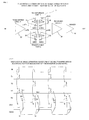
- Fig. 12 is a view showing the configuration of a background-art signal transfer device.
- the background-art signal transfer device is constituted by a transmitting circuit 200, a receiving circuit 300, and an insulating transformer 100 provided between the transmitting circuit 200 and the receiving circuit 300.
- a driver 400 is connected to a rear end of the receiving circuit 300.
- the insulating transformer 100 has a configuration in which two transformer parts, i.e.
- a transformer part 1 and a transformer part 2 are used so that a signal (set signal) indicating a turn-ON timing of the semiconductor power switch MH can be transmitted to an R1 terminal of the receiving circuit 300 through the transformer part 1 and a signal (reset signal) indicating a turn-OFF timing of the semiconductor power switch MH can be transmitted to an R2 terminal of the receiving circuit 300 through the transformer part 2.
- configuration is made so that output terminals of secondary-side windings of the transformer part 1 and the transformer part 2 can have the same magnetic polarity (voltages in the output terminals can change in the same direction when a magnetic flux changes in one and the same direction).
- the background-art signal transfer device in Fig. 12 drives the semiconductor power switch MH on the high side of the switching circuit shown in Fig. 11 , through the driver 400.
- Fig. 13 is a view showing an ideal operation waveform of the background-art signal transfer device shown in Fig. 12 .
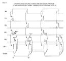
- Fig. 14 is an operation waveform view for explaining a problem of the background-art signal transfer device shown in Fig. 12 . Since Fig. 14 partially overlaps with Fig. 13 , operation of the background-art signal transfer device will be described with reference to Fig. 11 and Fig. 14 .
- a GND2 potential in Fig. 12 and Fig. 14 fluctuates in accordance with ON/OFF operations of power switches MH and ML.
- the GND2 potential drops from a high-side power supply voltage to GND1, as shown in Fig. 14 . Due to the fluctuation of the GND2, plus common-mode noises (N1 + and N2 + ) occur in the signal terminals R1 and R2 of the receiving circuit 300 side through parasitic capacitances (not shown).
- the GND2 potential rises from the GND1 to the high-side power supply voltage. Due to the fluctuation of the GND2, minus common-mode noises (N1 - and N2 - ) occur in the signal terminals R1 and R2 of the receiving circuit 300 side through the parasitic capacitances (not shown).
- the high-side power switch MH shown in Fig. 11 may turn ON/OFF by mistake due to any of the aforementioned common-mode noises.
- a circuit (not shown) for detecting the common-mode noise and suppressing generation of a false pulse is usually mounted inside the receiving circuit 300.
- JP-A-2013-51547 discloses a configuration in which a detection circuit for preventing malfunction from being caused by common-mode noise is mounted (see Paragraph [0058], Fig. 5 ).
- JP-A-3-44507 discloses a circuit configuration for preventing malfunction from being caused by common-mode noise (see Fig. 1 ).
- JP-A-2013-51547 has a problem that a receiving circuit becomes complicated and a malfunction preventing effect deteriorates as the fluctuation width of GND2 increases.
- JP-A-3-44507 also has a problem that a receiving circuit becomes complicated because a device such as a differential amplifier for canceling common-mode noise by subtraction of a common-mode voltage signal is required on the side of the receiving circuit.
- an object of the invention is to provide a signal transfer device for transferring a signal through an insulating transformer, in which occurrence of common-mode noise can be suppressed and a countermeasure circuit against the noise can be simplified.
- a signal transfer device which transfers a signal through a transformer, wherein: a secondary-side winding of one transformer part of the transformer connected to a set-side input terminal of a receiving circuit and a secondary-side winding of another transformer part of the transformer connected to a reset-side input terminal of the receiving circuit are magnetically coupled to each other so densely that a magnetic flux interlinking with one of the secondary-side windings can also interlink with the other; and the two secondary-side windings are connected to the receiving circuit so that the set-side input terminal and the reset-side input terminal of the receiving circuit can have magnetic polarities reverse to each other.
- a signal transfer device according to the first configuration of the invention, wherein: the two secondary-side windings are wound in one and the same direction but signal terminals and ground terminals of the two secondary-side windings are reversed to each other so that the set-side input terminal and the reset-side input terminal of the receiving circuit can have magnetic polarities reverse to each other.
- a signal transfer device according to the second configuration of the invention, wherein: the transformer is made up of rectangular, circular, elliptical or polygonal spiral coils.
- a signal transfer device according to the second configuration of the invention, wherein: the transformer is made up of rectangular, circular, elliptical or polygonal solenoid coils.
- a signal transfer device according to the second configuration of the invention, wherein: the transformer is made up of solenoid coils in which rectangular, circular, elliptical or polygonal spiral coils are laminated.
- a signal transfer device according to the first configuration of the invention, wherein: the two secondary-side windings are wound in reverse directions so that the set-side input terminal and the reset-side input terminal of the receiving circuit can have magnetic polarities reverse to each other.
- a signal transfer device according to the sixth configuration of the invention, wherein: the transformer is made up of rectangular, circular, elliptical or polygonal spiral coils.
- the transformer is made up of rectangular, circular, elliptical or polygonal solenoid coils.
- a ninth configuration of the invention there is provided a signal transfer device according to the sixth configuration of the invention, wherein: the transformer is made up of solenoid coils in which rectangular, circular, elliptical or polygonal spiral coils are laminated.
- a signal transfer device according to the second or sixth configuration of the invention, wherein: a primary-side winding is formed out of a single coil or out of a plurality of coils connected in series or in parallel.
- the transformer is made up of rectangular, circular, elliptical or polygonal spiral coils.
- a signal transfer device according to the tenth configuration of the invention, wherein: the transformer is made up of rectangular, circular, elliptical or polygonal solenoid coils.
- the transformer is made up of solenoid coils in which rectangular, circular, elliptical or polygonal spiral coils are laminated.
- a fourteenth configuration of the invention there is provided a signal transfer device according to the first configuration of the invention, wherein: a primary-side winding is formed out of one coil, and a signal transmitted to the set-side input terminal of the receiving circuit and a signal transmitted to the reset-side input terminal of the receiving circuit are inputted to opposite end terminals of the primary-side winding.
- a signal transfer device according to the second or fourteenth configuration of the invention, wherein: an intermediate tap is provided at a connection point at which one ends of the two secondary-side windings are connected to each other, and the other ends of the two secondary-side windings are connected to the set-side input terminal and the reset-side input terminal of the receiving circuit respectively.
- a signal transfer device has a basic configuration in which a secondary-side set winding and a secondary-side reset winding are magnetically coupled to thereby cancel in-phase changes in set and reset signals.
- a common mode which could occur in signal terminals R1 and R2 of a receiving circuit in the signal transfer device having the background-art configuration can be suppressed. Accordingly, it is possible to attain a function or an effect that a common-mode rejection unit (not shown) in a subsequent stage which was required in the background-art configuration can be dispensed with or the configuration of the common-mode rejection unit (not shown) can be simplified.
- Fig. 1 is a view showing the configuration of a signal transfer device according to a first embodiment of the invention.
- the signal transfer device according to the first embodiment shown in Fig. 1 serves for driving a high-side semiconductor power switch (not shown) of a switching power supply, an inverter, any of various driving circuits, etc.
- the signal transfer device according to the first embodiment is configured to include a transmitting circuit 20, a receiving circuit 30, and an insulating transformer 10 provided between the transmitting circuit 20 and the receiving circuit 30.
- the insulating transformer 10 provided between the transmitting circuit 20 and the receiving circuit 30 has two transformer parts (a transformer part 1 and a transformer part 2) so that the insulating transformer 10 can operate to transmit a signal (set signal) indicating a turn-ON timing through the transformer part 1 and transmit a signal (reset signal) indicating a turn-OFF timing through the transformer part 2.
- a secondary side (S1) of the set transformer part 1 and a secondary side (S2) of the reset transformer part 2 are magnetically coupled.
- the magnetic coupling direction is formed so that a secondary-side terminal (pinS1) of the transformer part 1 and a secondary-side terminal (pinS2) of the transformer part 2 can have reverse polarities (voltages in the output terminals can change in opposite directions to each other when a magnetic flux changes).
- a secondary-side set winding (S1) and a secondary-side reset winding (S2) are wound densely to share a core (including an air-core) so that a magnetic flux interlinking with one of the secondary-side set winding (S1) and the secondary-side reset winding (S2) can also interlink with the other of the secondary-side set winding (S1) and the secondary-side reset winding (S2).
- the winding direction of the secondary-side winding (S1) of the set-side transformer part 1 and the winding direction of the secondary-side winding (S2) of the reset-side transformer part 2 are made one and the same.
- the placement of one GND2 and one signal terminal (set or reset terminal) is made reverse to the placement of the secondary-side terminals (the other GND2 and the other signal terminal (reset or set terminal)) of the other transformer part so that the secondary-side terminal (pinS1) of the set-side transformer part 1 connected to the set terminal (R1) of the receiving circuit 30 and the secondary-side terminal (pinS2) of the reset-side transformer part 2 connected to the reset terminal (R2) of the receiving circuit 30 are magnetically coupled reversely.
- the placements of the secondary-side terminals (pinS1 and pinS2) of the two transformer parts are not reversed but the winding direction of the set-side secondary-side winding (S1) and the winding direction of the reset-side secondary-side winding (S2) are reserved so that the terminals can be magnetically coupled with reverse polarities.
- Fig. 2 is a view showing an operation waveform of the signal transfer device according to the first embodiment of the invention shown in Fig. 1 .
- a basic operation of the signal transfer device according to the first embodiment of the invention will be described with reference to Fig. 2 .
- the operation waveform of the background-art signal transfer device shown in Fig. 14 will be referred to here for suitable comparison.
- a signal for turning ON/OFF the semiconductor power switch such as an IGBT (Insulated Gate Bipolar Transistor) is inputted to an IN terminal of the transmitting circuit 20 in Fig. 1 .
- the transmitting circuit 20 outputs a set signal (T1) at a time t1 in Fig. 2 which is a leading edge timing of the signal of the IN terminal, a set signal (R1) is received by the receiving circuit 30 through the transformer part 1 at the time t1 in Fig. 2 .
- a reset signal (T2) is received by the receiving circuit 30 through the transformer part 2 at the time t2 in Fig. 2 .
- the receiving circuit 30 in Fig. 1 generates pulses OUT changing over between H (High) and L (Low) at receiving timings of the set signal (R1) and the reset signal (R2), and supplies the generated pulses OUT to a driver 40 in Fig. 1 .
- the driver 40 outputs the pulses for driving the semiconductor power switch (not shown) to a gate of the semiconductor power switch (not shown).
- the transformer parts are magnetically coupled with reverse polarities. Occurrence of common-mode noises which would occur in the secondary-side windings as in the background art can be therefore suppressed. That is, even when common-mode noises occur due to sudden changes in the GND2 potentials and the potentials of the signal terminals R1 and R2 tend to change in the same direction, magnetic fluxes occurring in the secondary-side windings act to cancel the changes of the potentials of the mated terminals respectively. Accordingly, occurrence of common-mode noises can be suppressed. Therefore, a common-mode rejection unit (not shown) in a subsequent stage can be dispensed with or the configuration of the common-mode rejection unit (not shown) can be simplified.
- Fig. 3 is a view showing the configuration of a signal transfer device according to a second embodiment of the invention.
- the signal transfer device according to the second embodiment shown in Fig. 3 serves for driving a high-side semiconductor power switch (not shown) of a switching power supply, an inverter, any of various driving circuits, etc. in the same manner as the signal transfer device shown in Fig. 1 .
- the signal transfer device according to the second embodiment is configured to include a transmitting circuit 20, a receiving circuit 30 and an insulating transformer 50 provided between the transmitting circuit 20 and the receiving circuit 30.
- the configuration of the insulating transformer 50 of the signal transfer device according to the second embodiment in Fig. 3 is different from the configuration of the insulating transformer 10 of the signal transfer device according to the first embodiment in Fig. 1 as follows. That is, in the configuration of the insulating transformer 50 shown in Fig. 3 , the number of primary-side windings formed in a transformer 3 is one, and an intermediate tap is provided between secondary-side windings and connected to GND2. Here, opposite ends of the primary-side winding serve as terminals to which a set signal and a reset signal are inputted from the transmitting circuit 20 respectively.
- the secondary-side windings may be regarded as a single secondary-side winding in which the two GND-side terminals of the secondary-side windings shown in Fig. 1 are connected to each other and an intermediate tap is provided in the connection point. Since the remaining configuration is the same as the configuration of the insulating transformer 10 of the signal transfer device according to the first embodiment shown in Fig. 1 , its description will be omitted here.
- Fig. 4 is a view showing a configuration example 1 in which the transformer according to the first embodiment shown in Fig. 1 is made up of spiral coils.
- each coil shown in Fig. 4 has a rectangular coil pattern, it may have a circular, elliptical or polygonal coil pattern.
- the winding directions of the primary-side and secondary-side windings of the coils are made common but the terminals disposed on the set side are made reverse to the terminals disposed on the reset side.
- Fig. 5 is a view showing a configuration example 2 in which the transformer according to the first embodiment shown in Fig. 1 is made up of spiral coils.
- each coil shown in Fig. 5 has a rectangular coil pattern, it may have a circular, elliptical or polygonal coil pattern.
- the winding directions of the primary-side and secondary-side windings of the coils are made reverse but the terminals disposed on the set side are made common to the terminals disposed on the reset side.
- Fig. 6 and Fig. 7 are views showing a configuration example 3 and a configuration example 4 in each of which the transformer according to the second embodiment shown in Fig. 3 is made up of spiral coils.
- each coil shown in each of Figs. 6 and 7 has a rectangular coil pattern, it may have a circular, elliptical or polygonal coil pattern.
- the transformer made up of the coil patterns shown in each of Figs. 4 to 7 is manufactured by a semiconductor technique, for example, the transformer can be formed in such a manner that the coil patterns are formed in three layers or four layers with interposition of an insulating layer between adjacent ones of the coil patterns.
- Fig. 8 is a view showing a configuration example 5 in which the transformer according to the second embodiment shown in Fig. 3 is made up of spiral coils.
- each coil shown in Fig. 8 has a rectangular coil pattern, it may have a circular, elliptical or polygonal coil pattern.
- the sequence of the primary-side winding (pinP1, pinP2), the set-side secondary winding (pinS1, GND2), and the reset-side secondary winding (GND2, pinS2) may be changed.
- the number of primary windings may be set as two or more. In this case, the primary windings, the set-side secondary winding and the reset-side secondary winding may be disposed alternately.
- connection to pinS1, pinP1 and GND2 may be made by multilayer wiring. That is, the connection can be formed in such a manner that the coil patterns in Fig. 8 are covered with an insulating film, opening portions (also referred to as through holes) are formed in the insulating film immediately above pinS1, pinP1 and GND2, and pinS1, pinP1 and GND2 are connected to wiring of an upper layer through the opening portions.
- the connection to pinS1, pinP1 and GND2 may be made by bonding wires.
- connection to pinS1, pinP1 and GND2 may be made by external wiring of a printed circuit etc.
- a not-shown connection portion connecting GND2 in two places (in the lower left and the center portions) in Fig. 8 corresponds to the intermediate tap in Fig. 3 .
- Fig. 9 is a view showing a configuration example 6 in which the transformer according to the first embodiment shown in Fig. 1 is made up of solenoid coils. Although each coil shown in Fig. 9 has a rectangular coil pattern, it may have a circular, elliptical or polygonal coil pattern.
- Fig. 10 is a view showing a configuration example 7 in which the transformer according to the second embodiment shown in Fig. 3 is made up of solenoid coils.
- each coil shown in Fig. 10 has a rectangular coil pattern, it may have a circular, elliptical or polygonal coil pattern.
Landscapes
- Engineering & Computer Science (AREA)
- Power Engineering (AREA)
- Multimedia (AREA)
- Power Conversion In General (AREA)
- Electronic Switches (AREA)
- Dc Digital Transmission (AREA)
Abstract
Description
- The present invention relates to a signal transfer device for driving a semiconductor power switch such as an IGBT (Insulated Gate Bipolar Transistor) provided on a high side of a switching power supply, an inverter or any of various drive circuits including a semiconductor switching element.
-
Fig. 11 is a view showing a configuration example of a typical switching power supply constituted by semiconductor power switches one of which includes a signal transfer device transferring a signal through an insulating transformer. For example, an IGBT, an MOSFET (Metal Oxide Field-Effect Transistor) etc. can be used as each of the semiconductor power switches. In a circuit for switching the semiconductor power switches, a high-side semiconductor power switch MH is driven to turn ON/OFF in accordance with an output from the signal transfer device through the insulating transformer. -
Fig. 12 is a view showing the configuration of a background-art signal transfer device. InFig. 12 , the background-art signal transfer device is constituted by atransmitting circuit 200, areceiving circuit 300, and aninsulating transformer 100 provided between thetransmitting circuit 200 and thereceiving circuit 300. In addition, adriver 400 is connected to a rear end of thereceiving circuit 300. Further, theinsulating transformer 100 has a configuration in which two transformer parts, i.e. atransformer part 1 and atransformer part 2, are used so that a signal (set signal) indicating a turn-ON timing of the semiconductor power switch MH can be transmitted to an R1 terminal of thereceiving circuit 300 through thetransformer part 1 and a signal (reset signal) indicating a turn-OFF timing of the semiconductor power switch MH can be transmitted to an R2 terminal of thereceiving circuit 300 through thetransformer part 2. As shown inFig. 12 , configuration is made so that output terminals of secondary-side windings of thetransformer part 1 and thetransformer part 2 can have the same magnetic polarity (voltages in the output terminals can change in the same direction when a magnetic flux changes in one and the same direction). The background-art signal transfer device inFig. 12 drives the semiconductor power switch MH on the high side of the switching circuit shown inFig. 11 , through thedriver 400. -
Fig. 13 is a view showing an ideal operation waveform of the background-art signal transfer device shown inFig. 12 .Fig. 14 is an operation waveform view for explaining a problem of the background-art signal transfer device shown inFig. 12 . SinceFig. 14 partially overlaps withFig. 13 , operation of the background-art signal transfer device will be described with reference toFig. 11 andFig. 14 . - When the high-side power switch MH shown in
Fig. 11 is driven, a GND2 potential inFig. 12 andFig. 14 fluctuates in accordance with ON/OFF operations of power switches MH and ML. When the power switch MH turns OFF and the power switch ML turns ON due to an output from the signal transfer device, the GND2 potential drops from a high-side power supply voltage to GND1, as shown inFig. 14 . Due to the fluctuation of the GND2, plus common-mode noises (N1+ and N2+) occur in the signal terminals R1 and R2 of thereceiving circuit 300 side through parasitic capacitances (not shown). - On the other hand, when the power switch ML turns OFF and the power switch MH turns ON due to an output from the signal transfer device, the GND2 potential rises from the GND1 to the high-side power supply voltage. Due to the fluctuation of the GND2, minus common-mode noises (N1- and N2-) occur in the signal terminals R1 and R2 of the
receiving circuit 300 side through the parasitic capacitances (not shown). - In some cases, the high-side power switch MH shown in
Fig. 11 may turn ON/OFF by mistake due to any of the aforementioned common-mode noises. - In the background art in order to prevent malfunction from being caused by common-mode noise, a circuit (not shown) for detecting the common-mode noise and suppressing generation of a false pulse is usually mounted inside the
receiving circuit 300. -
JP-A-2013-51547 Fig. 5 ). -
JP-A-3-44507 Fig. 1 ). - The aforementioned configuration described in
JP-A-2013-51547 - In addition, the configuration described in
JP-A-3-44507 - Therefore, an object of the invention is to provide a signal transfer device for transferring a signal through an insulating transformer, in which occurrence of common-mode noise can be suppressed and a countermeasure circuit against the noise can be simplified.
- In order to solve the foregoing problem, according to a first configuration of the invention, there is provided a signal transfer device which transfers a signal through a transformer, wherein: a secondary-side winding of one transformer part of the transformer connected to a set-side input terminal of a receiving circuit and a secondary-side winding of another transformer part of the transformer connected to a reset-side input terminal of the receiving circuit are magnetically coupled to each other so densely that a magnetic flux interlinking with one of the secondary-side windings can also interlink with the other; and the two secondary-side windings are connected to the receiving circuit so that the set-side input terminal and the reset-side input terminal of the receiving circuit can have magnetic polarities reverse to each other.
- According to a second configuration of the invention, there is provided a signal transfer device according to the first configuration of the invention, wherein: the two secondary-side windings are wound in one and the same direction but signal terminals and ground terminals of the two secondary-side windings are reversed to each other so that the set-side input terminal and the reset-side input terminal of the receiving circuit can have magnetic polarities reverse to each other.
- According to a third configuration of the invention, there is provided a signal transfer device according to the second configuration of the invention, wherein: the transformer is made up of rectangular, circular, elliptical or polygonal spiral coils.
- According to a fourth configuration of the invention, there is provided a signal transfer device according to the second configuration of the invention, wherein: the transformer is made up of rectangular, circular, elliptical or polygonal solenoid coils.
- According to a fifth configuration of the invention, there is provided a signal transfer device according to the second configuration of the invention, wherein: the transformer is made up of solenoid coils in which rectangular, circular, elliptical or polygonal spiral coils are laminated.
- According to a sixth configuration of the invention, there is provided a signal transfer device according to the first configuration of the invention, wherein: the two secondary-side windings are wound in reverse directions so that the set-side input terminal and the reset-side input terminal of the receiving circuit can have magnetic polarities reverse to each other.
- According to a seventh configuration of the invention, there is provided a signal transfer device according to the sixth configuration of the invention, wherein: the transformer is made up of rectangular, circular, elliptical or polygonal spiral coils.
- According to an eighth configuration of the invention, there is provided a signal transfer device according to the sixth configuration of the invention, wherein: the transformer is made up of rectangular, circular, elliptical or polygonal solenoid coils.
- According to a ninth configuration of the invention, there is provided a signal transfer device according to the sixth configuration of the invention, wherein: the transformer is made up of solenoid coils in which rectangular, circular, elliptical or polygonal spiral coils are laminated.
- According to a tenth configuration of the invention, there is provided a signal transfer device according to the second or sixth configuration of the invention, wherein: a primary-side winding is formed out of a single coil or out of a plurality of coils connected in series or in parallel.
- According to an eleventh configuration of the invention, there is provided a signal transfer device according to the tenth configuration of the invention, wherein: the transformer is made up of rectangular, circular, elliptical or polygonal spiral coils.
- According to a twelfth configuration of the invention, there is provided a signal transfer device according to the tenth configuration of the invention, wherein: the transformer is made up of rectangular, circular, elliptical or polygonal solenoid coils.
- According to a thirteenth configuration of the invention, there is provided a signal transfer device according to the tenth configuration of the invention, wherein: the transformer is made up of solenoid coils in which rectangular, circular, elliptical or polygonal spiral coils are laminated.
- According to a fourteenth configuration of the invention, there is provided a signal transfer device according to the first configuration of the invention, wherein: a primary-side winding is formed out of one coil, and a signal transmitted to the set-side input terminal of the receiving circuit and a signal transmitted to the reset-side input terminal of the receiving circuit are inputted to opposite end terminals of the primary-side winding.
- According to a fifteenth configuration of the invention, there is provided a signal transfer device according to the second or fourteenth configuration of the invention, wherein: an intermediate tap is provided at a connection point at which one ends of the two secondary-side windings are connected to each other, and the other ends of the two secondary-side windings are connected to the set-side input terminal and the reset-side input terminal of the receiving circuit respectively.
- According to the invention, it is possible to suppress occurrence of common-mode noise and simplify a countermeasure circuit against the noise in the signal transfer device transferring a signal through the insulating transformer.
-
-
Fig. 1 is a view showing the configuration of a signal transfer device according to a first embodiment of the invention; -
Fig. 2 is a view showing a basic operation waveform of the signal transfer device according to the first embodiment of the invention shown inFig. 1 ; -
Fig. 3 is a view showing the configuration of a signal transfer device according to a second embodiment of the invention; -
Fig. 4 is a view showing a configuration example (Example 1) in which a transformer in the first embodiment shown inFig. 1 is made up of spiral coils; -
Fig. 5 is a view showing a configuration example (Example 2) in which a transformer in the first embodiment shown inFig. 1 is made up of spiral coils; -
Fig. 6 is a view showing a configuration example (Example 3) in which a transformer in the second embodiment shown inFig. 3 is made up of spiral coils; -
Fig. 7 is a view showing a configuration example (Example 4) in which a transformer in the second embodiment shown inFig. 3 is made up of spiral coils; -
Fig. 8 is a view showing a configuration example (Example 5) in which a transformer in the second embodiment shown inFig. 3 is made up of spiral coils; -
Fig. 9 is a view showing a configuration example (Example 6) in which a transformer in the first embodiment shown inFig. 1 is made up of solenoid coils; -
Fig. 10 is a view showing a configuration example (Example 7) in which a transformer in the second embodiment shown inFig. 3 is made up of solenoid coils; -
Fig. 11 is a view showing a configuration example of a typical switching power supply constituted by semiconductor power switches one of which includes a signal transfer device transferring a signal through an insulating transformer; -
Fig. 12 is a view showing the configuration of a background-art signal transfer device; -
Fig. 13 is a view showing an ideal operation waveform of the background-art signal transfer device shown inFig. 12 ; and -
Fig. 14 is an operation waveform diagram for explaining a problem of the background-art signal transfer device shown inFig. 12 . - Embodiments of the invention will be described below in detail.
- A signal transfer device according to each of embodiments of the invention has a basic configuration in which a secondary-side set winding and a secondary-side reset winding are magnetically coupled to thereby cancel in-phase changes in set and reset signals. When the configuration is made thus, a common mode which could occur in signal terminals R1 and R2 of a receiving circuit in the signal transfer device having the background-art configuration can be suppressed. Accordingly, it is possible to attain a function or an effect that a common-mode rejection unit (not shown) in a subsequent stage which was required in the background-art configuration can be dispensed with or the configuration of the common-mode rejection unit (not shown) can be simplified.
-
Fig. 1 is a view showing the configuration of a signal transfer device according to a first embodiment of the invention. The signal transfer device according to the first embodiment shown inFig. 1 serves for driving a high-side semiconductor power switch (not shown) of a switching power supply, an inverter, any of various driving circuits, etc. In order to transfer a signal for driving the high-side semiconductor power switch, the signal transfer device according to the first embodiment is configured to include a transmittingcircuit 20, a receivingcircuit 30, and an insulatingtransformer 10 provided between the transmittingcircuit 20 and the receivingcircuit 30. - As shown in
Fig. 1 , the insulatingtransformer 10 provided between the transmittingcircuit 20 and the receivingcircuit 30 has two transformer parts (atransformer part 1 and a transformer part 2) so that the insulatingtransformer 10 can operate to transmit a signal (set signal) indicating a turn-ON timing through thetransformer part 1 and transmit a signal (reset signal) indicating a turn-OFF timing through thetransformer part 2. - In the insulating
transformer 10 inFig. 1 , a secondary side (S1) of theset transformer part 1 and a secondary side (S2) of thereset transformer part 2 are magnetically coupled. The magnetic coupling direction is formed so that a secondary-side terminal (pinS1) of thetransformer part 1 and a secondary-side terminal (pinS2) of thetransformer part 2 can have reverse polarities (voltages in the output terminals can change in opposite directions to each other when a magnetic flux changes). Specifically, a secondary-side set winding (S1) and a secondary-side reset winding (S2) are wound densely to share a core (including an air-core) so that a magnetic flux interlinking with one of the secondary-side set winding (S1) and the secondary-side reset winding (S2) can also interlink with the other of the secondary-side set winding (S1) and the secondary-side reset winding (S2). The winding direction of the secondary-side winding (S1) of the set-side transformer part 1 and the winding direction of the secondary-side winding (S2) of the reset-side transformer part 2 are made one and the same. - That is, of two pairs of secondary-side terminals (two GND2 and two signal terminals (set and reset terminals)), the placement of one GND2 and one signal terminal (set or reset terminal) is made reverse to the placement of the secondary-side terminals (the other GND2 and the other signal terminal (reset or set terminal)) of the other transformer part so that the secondary-side terminal (pinS1) of the set-
side transformer part 1 connected to the set terminal (R1) of the receivingcircuit 30 and the secondary-side terminal (pinS2) of the reset-side transformer part 2 connected to the reset terminal (R2) of the receivingcircuit 30 are magnetically coupled reversely. Alternatively, the placements of the secondary-side terminals (pinS1 and pinS2) of the two transformer parts (theset transformer part 1 and the reset transformer part 2) are not reversed but the winding direction of the set-side secondary-side winding (S1) and the winding direction of the reset-side secondary-side winding (S2) are reserved so that the terminals can be magnetically coupled with reverse polarities. -
Fig. 2 is a view showing an operation waveform of the signal transfer device according to the first embodiment of the invention shown inFig. 1 . A basic operation of the signal transfer device according to the first embodiment of the invention will be described with reference toFig. 2 . The operation waveform of the background-art signal transfer device shown inFig. 14 will be referred to here for suitable comparison. - Description about
Fig. 1 and Fig. 2 will be made in detail as follows. That is, a signal for turning ON/OFF the semiconductor power switch (not shown) such as an IGBT (Insulated Gate Bipolar Transistor) is inputted to an IN terminal of the transmittingcircuit 20 inFig. 1 . When the transmittingcircuit 20 outputs a set signal (T1) at a time t1 inFig. 2 which is a leading edge timing of the signal of the IN terminal, a set signal (R1) is received by the receivingcircuit 30 through thetransformer part 1 at the time t1 inFig. 2 . - When the transmitting
circuit 20 inFig. 1 outputs a reset signal (T2) at a time t2 inFig. 2 which is a trailing edge timing of the signal of the IN terminal, a reset signal (R2) is received by the receivingcircuit 30 through thetransformer part 2 at the time t2 inFig. 2 . - The receiving
circuit 30 inFig. 1 generates pulses OUT changing over between H (High) and L (Low) at receiving timings of the set signal (R1) and the reset signal (R2), and supplies the generated pulses OUT to adriver 40 inFig. 1 . Thedriver 40 outputs the pulses for driving the semiconductor power switch (not shown) to a gate of the semiconductor power switch (not shown). - In the signal transfer device according to the first embodiment of the invention, the transformer parts are magnetically coupled with reverse polarities. Occurrence of common-mode noises which would occur in the secondary-side windings as in the background art can be therefore suppressed. That is, even when common-mode noises occur due to sudden changes in the GND2 potentials and the potentials of the signal terminals R1 and R2 tend to change in the same direction, magnetic fluxes occurring in the secondary-side windings act to cancel the changes of the potentials of the mated terminals respectively. Accordingly, occurrence of common-mode noises can be suppressed. Therefore, a common-mode rejection unit (not shown) in a subsequent stage can be dispensed with or the configuration of the common-mode rejection unit (not shown) can be simplified.
-
Fig. 3 is a view showing the configuration of a signal transfer device according to a second embodiment of the invention. The signal transfer device according to the second embodiment shown inFig. 3 serves for driving a high-side semiconductor power switch (not shown) of a switching power supply, an inverter, any of various driving circuits, etc. in the same manner as the signal transfer device shown inFig. 1 . In order to transfer a signal for driving the high-side semiconductor power switch, the signal transfer device according to the second embodiment is configured to include a transmittingcircuit 20, a receivingcircuit 30 and an insulatingtransformer 50 provided between the transmittingcircuit 20 and the receivingcircuit 30. - The configuration of the insulating
transformer 50 of the signal transfer device according to the second embodiment inFig. 3 is different from the configuration of the insulatingtransformer 10 of the signal transfer device according to the first embodiment inFig. 1 as follows. That is, in the configuration of the insulatingtransformer 50 shown inFig. 3 , the number of primary-side windings formed in atransformer 3 is one, and an intermediate tap is provided between secondary-side windings and connected to GND2. Here, opposite ends of the primary-side winding serve as terminals to which a set signal and a reset signal are inputted from the transmittingcircuit 20 respectively. In addition, the secondary-side windings may be regarded as a single secondary-side winding in which the two GND-side terminals of the secondary-side windings shown inFig. 1 are connected to each other and an intermediate tap is provided in the connection point. Since the remaining configuration is the same as the configuration of the insulatingtransformer 10 of the signal transfer device according to the first embodiment shown inFig. 1 , its description will be omitted here. -
Fig. 4 is a view showing a configuration example 1 in which the transformer according to the first embodiment shown inFig. 1 is made up of spiral coils. Although each coil shown inFig. 4 has a rectangular coil pattern, it may have a circular, elliptical or polygonal coil pattern. The winding directions of the primary-side and secondary-side windings of the coils are made common but the terminals disposed on the set side are made reverse to the terminals disposed on the reset side. -
Fig. 5 is a view showing a configuration example 2 in which the transformer according to the first embodiment shown inFig. 1 is made up of spiral coils. Although each coil shown inFig. 5 has a rectangular coil pattern, it may have a circular, elliptical or polygonal coil pattern. The winding directions of the primary-side and secondary-side windings of the coils are made reverse but the terminals disposed on the set side are made common to the terminals disposed on the reset side. -
Fig. 6 andFig. 7 are views showing a configuration example 3 and a configuration example 4 in each of which the transformer according to the second embodiment shown inFig. 3 is made up of spiral coils. Although each coil shown in each ofFigs. 6 and7 has a rectangular coil pattern, it may have a circular, elliptical or polygonal coil pattern. - When the transformer made up of the coil patterns shown in each of
Figs. 4 to 7 is manufactured by a semiconductor technique, for example, the transformer can be formed in such a manner that the coil patterns are formed in three layers or four layers with interposition of an insulating layer between adjacent ones of the coil patterns. -
Fig. 8 is a view showing a configuration example 5 in which the transformer according to the second embodiment shown inFig. 3 is made up of spiral coils. Although each coil shown inFig. 8 has a rectangular coil pattern, it may have a circular, elliptical or polygonal coil pattern. In addition, inFig. 8 , the sequence of the primary-side winding (pinP1, pinP2), the set-side secondary winding (pinS1, GND2), and the reset-side secondary winding (GND2, pinS2) may be changed. Further, the number of primary windings may be set as two or more. In this case, the primary windings, the set-side secondary winding and the reset-side secondary winding may be disposed alternately. - When the transformer made up of the coil patterns shown in
Fig. 8 is manufactured by a semiconductor technique, for example, the transformer can be manufactured in such a manner that all the coil patterns are formed in the same layer. In this case, connection to pinS1, pinP1 and GND2 may be made by multilayer wiring. That is, the connection can be formed in such a manner that the coil patterns inFig. 8 are covered with an insulating film, opening portions (also referred to as through holes) are formed in the insulating film immediately above pinS1, pinP1 and GND2, and pinS1, pinP1 and GND2 are connected to wiring of an upper layer through the opening portions. In addition, the connection to pinS1, pinP1 and GND2 may be made by bonding wires. Moreover, the connection to pinS1, pinP1 and GND2 may be made by external wiring of a printed circuit etc. Further, a not-shown connection portion connecting GND2 in two places (in the lower left and the center portions) inFig. 8 corresponds to the intermediate tap inFig. 3 . -
Fig. 9 is a view showing a configuration example 6 in which the transformer according to the first embodiment shown inFig. 1 is made up of solenoid coils. Although each coil shown inFig. 9 has a rectangular coil pattern, it may have a circular, elliptical or polygonal coil pattern. -
Fig. 10 is a view showing a configuration example 7 in which the transformer according to the second embodiment shown inFig. 3 is made up of solenoid coils. Although each coil shown inFig. 10 has a rectangular coil pattern, it may have a circular, elliptical or polygonal coil pattern.
Claims (15)
- A signal transfer device which transfers a signal through a transformer (10), wherein:a secondary-side winding (S1) of one transformer part (1) of the transformer (10) connected to a set-side input terminal (R1) of a receiving circuit (30) and a secondary-side winding (S2) of another transformer part (2) of the transformer (10) connected to a reset-side input terminal (R2) of the receiving circuit (30) are magnetically coupled to each other so densely that a magnetic flux interlinking with one of the secondary-side windings (S1, S2) can also interlink with the other; and the two secondary-side windings (S1, S2) are connected to the receiving circuit (30) so that the set-side input terminal (R1) and the reset-side input terminal (R2) of the receiving circuit (30) can have magnetic polarities reverse to each other.
- The signal transfer device according to Claim 1, wherein:the two secondary-side windings (S1, S2) are wound in one and the same direction but signal terminals (pinS1, pinS2) and ground terminals (GND2) of the two secondary-side windings (S1, S2) are reversed to each other so that the set-side input terminal (R1) and the reset-side input terminal (R2) of the receiving circuit (30) can have magnetic polarities reverse to each other.
- The signal transfer device according to Claim 2, wherein:the transformer (10) is made up of rectangular, circular, elliptical or polygonal spiral coils.
- The signal transfer device according to Claim 2, wherein:the transformer (10) is made up of rectangular, circular, elliptical or polygonal solenoid coils.
- The signal transfer device according to Claim 2, wherein:the transformer (10) is made up of solenoid coils in which rectangular, circular, elliptical or polygonal spiral coils are laminated.
- The signal transfer device according to Claim 1, wherein:the two secondary-side windings (S1, S2) are wound in reverse directions so that the set-side input terminal (R1) and the reset-side input terminal (R2) of the receiving circuit (30) can have magnetic polarities reverse to each other.
- The signal transfer device according to Claim 6, wherein:the transformer (10) is made up of rectangular, circular, elliptical or polygonal spiral coils.
- The signal transfer device according to Claim 6, wherein:the transformer (10) is made up of rectangular, circular, elliptical or polygonal solenoid coils.
- The signal transfer device according to Claim 6, wherein:the transformer (10) is made up of solenoid coils in which rectangular, circular, elliptical or polygonal spiral coils are laminated.
- The signal transfer device according to Claim 2 or 6, wherein:a primary-side winding (P1, P2) is formed out of a single coil or out of a plurality of coils connected in series or in parallel.
- The signal transfer device according to Claim 10, wherein:the transformer (10) is made up of rectangular, circular, elliptical or polygonal spiral coils.
- The signal transfer device according to Claim 10, wherein:the transformer (10) is made up of rectangular, circular, elliptical or polygonal solenoid coils.
- The signal transfer device according to Claim 10, wherein:the transformer (10) is made up of solenoid coils in which rectangular, circular, elliptical or polygonal spiral coils are laminated.
- The signal transfer device according to Claim 1, wherein:a primary-side winding (P1, P2) is formed out of one coil, and a signal transmitted to the set-side input terminal (R1) of the receiving circuit (30) and a signal transmitted to the reset-side input terminal (R2) of the receiving circuit (30) are inputted to opposite end terminals of the primary-side winding (P1, P2).
- The signal transfer device according to Claim 2 or 14, wherein:an intermediate tap is provided at a connection point at which one ends of the two secondary-side windings (S1, S2) are connected to each other, and the other ends of the two secondary-side windings (S1, S2) are connected to the set-side input terminal (R1) and the reset-side input terminal (R2) of the receiving circuit (30) respectively.
Applications Claiming Priority (1)
| Application Number | Priority Date | Filing Date | Title |
|---|---|---|---|
| JP2014243529A JP6582401B2 (en) | 2014-12-01 | 2014-12-01 | Signal transmission device |
Publications (2)
| Publication Number | Publication Date |
|---|---|
| EP3032551A1 true EP3032551A1 (en) | 2016-06-15 |
| EP3032551B1 EP3032551B1 (en) | 2020-07-22 |
Family
ID=54542118
Family Applications (1)
| Application Number | Title | Priority Date | Filing Date |
|---|---|---|---|
| EP15194544.1A Active EP3032551B1 (en) | 2014-12-01 | 2015-11-13 | Signal transfer device |
Country Status (3)
| Country | Link |
|---|---|
| US (1) | US9899146B2 (en) |
| EP (1) | EP3032551B1 (en) |
| JP (1) | JP6582401B2 (en) |
Families Citing this family (2)
| Publication number | Priority date | Publication date | Assignee | Title |
|---|---|---|---|---|
| JP7051649B2 (en) | 2018-09-07 | 2022-04-11 | 株式会社東芝 | Magnetic coupling device and communication system |
| JP7366849B2 (en) | 2020-07-09 | 2023-10-23 | 株式会社東芝 | Communication device |
Citations (11)
| Publication number | Priority date | Publication date | Assignee | Title |
|---|---|---|---|---|
| EP0410526A1 (en) * | 1989-07-28 | 1991-01-30 | Koninklijke Philips Electronics N.V. | Generator for generating an electric voltage |
| JPH0344507A (en) | 1989-07-12 | 1991-02-26 | Toshiba Corp | Analog input circuit |
| US5892667A (en) * | 1994-06-17 | 1999-04-06 | Equi-Tech Licensing Corp. | Symmetrical power system |
| US6278266B1 (en) * | 1994-06-17 | 2001-08-21 | Martin S. Glasband | Symmetrical power generator and method of use |
| US20030042571A1 (en) * | 1997-10-23 | 2003-03-06 | Baoxing Chen | Chip-scale coils and isolators based thereon |
| US20040140877A1 (en) * | 2002-07-26 | 2004-07-22 | Fumiaki Nakao | Microconverter and laminated magnetic-core inductor |
| US20040196132A1 (en) * | 2003-04-04 | 2004-10-07 | Jay Yu | Transformer formed between two layout layers |
| US20110291819A1 (en) * | 2009-02-20 | 2011-12-01 | Shunichi Kaeriyama | Reception circuit and signal reception method |
| US20120020419A1 (en) * | 2009-03-31 | 2012-01-26 | Shunichi Kaeriyama | Semiconductor device |
| JP2012182740A (en) * | 2011-03-02 | 2012-09-20 | Nitto Denko Corp | Circuit board for isolator, isolator, and manufacturing method of circuit board and isolator |
| JP2013051547A (en) | 2011-08-31 | 2013-03-14 | Renesas Electronics Corp | Semiconductor integrated circuit and driving device including the same |
Family Cites Families (11)
| Publication number | Priority date | Publication date | Assignee | Title |
|---|---|---|---|---|
| JPS5320211Y2 (en) * | 1972-02-12 | 1978-05-27 | ||
| JPS5830223A (en) * | 1981-08-17 | 1983-02-22 | Matsushita Electric Ind Co Ltd | Isolated transmission equipment for digital signals |
| JPS61176823U (en) * | 1985-04-23 | 1986-11-05 | ||
| JP3351172B2 (en) * | 1995-05-23 | 2002-11-25 | 松下電器産業株式会社 | Thin transformer |
| JP2005347286A (en) * | 2002-05-29 | 2005-12-15 | Ajinomoto Co Inc | Multilayered substrate with built-in coil, semiconductor chip, and manufacturing method thereof |
| JP4894604B2 (en) * | 2007-04-27 | 2012-03-14 | 富士電機株式会社 | Air-core type insulation transformer, signal transmission circuit and power conversion device using air-core type insulation transformer |
| KR20110016875A (en) * | 2008-04-01 | 2011-02-18 | 아식 어드밴티지 인코포레이티드 | Pulse transformer driver |
| JP5253012B2 (en) * | 2008-06-24 | 2013-07-31 | ローム株式会社 | Power semiconductor drive circuit device and signal transmission circuit device used therefor |
| JP4737268B2 (en) * | 2008-10-31 | 2011-07-27 | Tdk株式会社 | Surface mount pulse transformer and method and apparatus for manufacturing the same |
| JP5800691B2 (en) | 2011-11-25 | 2015-10-28 | ルネサスエレクトロニクス株式会社 | Trance |
| JP6048052B2 (en) * | 2012-10-11 | 2016-12-21 | 富士電機株式会社 | Signal transmission device and switching power supply device |
-
2014
- 2014-12-01 JP JP2014243529A patent/JP6582401B2/en not_active Expired - Fee Related
-
2015
- 2015-11-13 EP EP15194544.1A patent/EP3032551B1/en active Active
- 2015-11-16 US US14/942,764 patent/US9899146B2/en not_active Expired - Fee Related
Patent Citations (11)
| Publication number | Priority date | Publication date | Assignee | Title |
|---|---|---|---|---|
| JPH0344507A (en) | 1989-07-12 | 1991-02-26 | Toshiba Corp | Analog input circuit |
| EP0410526A1 (en) * | 1989-07-28 | 1991-01-30 | Koninklijke Philips Electronics N.V. | Generator for generating an electric voltage |
| US5892667A (en) * | 1994-06-17 | 1999-04-06 | Equi-Tech Licensing Corp. | Symmetrical power system |
| US6278266B1 (en) * | 1994-06-17 | 2001-08-21 | Martin S. Glasband | Symmetrical power generator and method of use |
| US20030042571A1 (en) * | 1997-10-23 | 2003-03-06 | Baoxing Chen | Chip-scale coils and isolators based thereon |
| US20040140877A1 (en) * | 2002-07-26 | 2004-07-22 | Fumiaki Nakao | Microconverter and laminated magnetic-core inductor |
| US20040196132A1 (en) * | 2003-04-04 | 2004-10-07 | Jay Yu | Transformer formed between two layout layers |
| US20110291819A1 (en) * | 2009-02-20 | 2011-12-01 | Shunichi Kaeriyama | Reception circuit and signal reception method |
| US20120020419A1 (en) * | 2009-03-31 | 2012-01-26 | Shunichi Kaeriyama | Semiconductor device |
| JP2012182740A (en) * | 2011-03-02 | 2012-09-20 | Nitto Denko Corp | Circuit board for isolator, isolator, and manufacturing method of circuit board and isolator |
| JP2013051547A (en) | 2011-08-31 | 2013-03-14 | Renesas Electronics Corp | Semiconductor integrated circuit and driving device including the same |
Also Published As
| Publication number | Publication date |
|---|---|
| US20160155565A1 (en) | 2016-06-02 |
| JP2016111374A (en) | 2016-06-20 |
| EP3032551B1 (en) | 2020-07-22 |
| JP6582401B2 (en) | 2019-10-02 |
| US9899146B2 (en) | 2018-02-20 |
Similar Documents
| Publication | Publication Date | Title |
|---|---|---|
| US6720816B2 (en) | Integratable circuit configuration for potential-free signal transmission | |
| CN107210667B (en) | High-frequency insulation gate driving circuit and grid circuit driving method | |
| JP5375952B2 (en) | Semiconductor device | |
| JP4528841B2 (en) | Power converter | |
| EP3108581B1 (en) | Switch controller with validation circuit for improved noise immunity | |
| JP2009232637A (en) | Switch controller and motor drive using the same | |
| US20130285465A1 (en) | Transmitter circuit and semiconductor integrated circuit having the same | |
| CN106130322B (en) | Gate driving circuit for reducing parasitic coupling | |
| JP5990887B2 (en) | Gate drive circuit | |
| US20090057039A1 (en) | Electronic circuit | |
| US20230238964A1 (en) | Transmission circuit | |
| WO2016189585A1 (en) | Power conversion device | |
| US9899146B2 (en) | Signal transfer device | |
| US20170063213A1 (en) | Flyback converter | |
| US9606567B2 (en) | Method and apparatus for providing electrical isolation | |
| US10490135B2 (en) | Enable signal generation circuit, power conversion circuit and display device | |
| JP5795927B2 (en) | Switching power supply | |
| CN109962621B (en) | Power supply conversion device | |
| CN109712785A (en) | Potential device, switch driving circuit and pulse power system is isolated | |
| WO2017099191A1 (en) | Signal transfer circuit | |
| US20240347446A1 (en) | Lateral coils used for energy transfer over isolation region in multi-voltage devices | |
| JP6942998B2 (en) | Transformer parts and drive | |
| CN118055692A (en) | Electronic equipment | |
| JP2024092549A (en) | Signal transmission circuit control system, I/O module equipped with the same, control method, and control program | |
| WO2021117432A1 (en) | Signal transmission circuit |
Legal Events
| Date | Code | Title | Description |
|---|---|---|---|
| PUAI | Public reference made under article 153(3) epc to a published international application that has entered the european phase |
Free format text: ORIGINAL CODE: 0009012 |
|
| AK | Designated contracting states |
Kind code of ref document: A1 Designated state(s): AL AT BE BG CH CY CZ DE DK EE ES FI FR GB GR HR HU IE IS IT LI LT LU LV MC MK MT NL NO PL PT RO RS SE SI SK SM TR |
|
| AX | Request for extension of the european patent |
Extension state: BA ME |
|
| STAA | Information on the status of an ep patent application or granted ep patent |
Free format text: STATUS: REQUEST FOR EXAMINATION WAS MADE |
|
| 17P | Request for examination filed |
Effective date: 20161215 |
|
| RBV | Designated contracting states (corrected) |
Designated state(s): AL AT BE BG CH CY CZ DE DK EE ES FI FR GB GR HR HU IE IS IT LI LT LU LV MC MK MT NL NO PL PT RO RS SE SI SK SM TR |
|
| STAA | Information on the status of an ep patent application or granted ep patent |
Free format text: STATUS: EXAMINATION IS IN PROGRESS |
|
| 17Q | First examination report despatched |
Effective date: 20170524 |
|
| GRAP | Despatch of communication of intention to grant a patent |
Free format text: ORIGINAL CODE: EPIDOSNIGR1 |
|
| STAA | Information on the status of an ep patent application or granted ep patent |
Free format text: STATUS: GRANT OF PATENT IS INTENDED |
|
| INTG | Intention to grant announced |
Effective date: 20200211 |
|
| GRAS | Grant fee paid |
Free format text: ORIGINAL CODE: EPIDOSNIGR3 |
|
| GRAA | (expected) grant |
Free format text: ORIGINAL CODE: 0009210 |
|
| STAA | Information on the status of an ep patent application or granted ep patent |
Free format text: STATUS: THE PATENT HAS BEEN GRANTED |
|
| AK | Designated contracting states |
Kind code of ref document: B1 Designated state(s): AL AT BE BG CH CY CZ DE DK EE ES FI FR GB GR HR HU IE IS IT LI LT LU LV MC MK MT NL NO PL PT RO RS SE SI SK SM TR |
|
| REG | Reference to a national code |
Ref country code: GB Ref legal event code: FG4D |
|
| RIN1 | Information on inventor provided before grant (corrected) |
Inventor name: SUGAHARA, SATOSHI |
|
| REG | Reference to a national code |
Ref country code: CH Ref legal event code: EP |
|
| REG | Reference to a national code |
Ref country code: DE Ref legal event code: R096 Ref document number: 602015056065 Country of ref document: DE |
|
| REG | Reference to a national code |
Ref country code: AT Ref legal event code: REF Ref document number: 1294182 Country of ref document: AT Kind code of ref document: T Effective date: 20200815 |
|
| REG | Reference to a national code |
Ref country code: IE Ref legal event code: FG4D |
|
| REG | Reference to a national code |
Ref country code: LT Ref legal event code: MG4D |
|
| REG | Reference to a national code |
Ref country code: AT Ref legal event code: MK05 Ref document number: 1294182 Country of ref document: AT Kind code of ref document: T Effective date: 20200722 |
|
| PG25 | Lapsed in a contracting state [announced via postgrant information from national office to epo] |
Ref country code: FI Free format text: LAPSE BECAUSE OF FAILURE TO SUBMIT A TRANSLATION OF THE DESCRIPTION OR TO PAY THE FEE WITHIN THE PRESCRIBED TIME-LIMIT Effective date: 20200722 Ref country code: HR Free format text: LAPSE BECAUSE OF FAILURE TO SUBMIT A TRANSLATION OF THE DESCRIPTION OR TO PAY THE FEE WITHIN THE PRESCRIBED TIME-LIMIT Effective date: 20200722 Ref country code: PT Free format text: LAPSE BECAUSE OF FAILURE TO SUBMIT A TRANSLATION OF THE DESCRIPTION OR TO PAY THE FEE WITHIN THE PRESCRIBED TIME-LIMIT Effective date: 20201123 Ref country code: LT Free format text: LAPSE BECAUSE OF FAILURE TO SUBMIT A TRANSLATION OF THE DESCRIPTION OR TO PAY THE FEE WITHIN THE PRESCRIBED TIME-LIMIT Effective date: 20200722 Ref country code: GR Free format text: LAPSE BECAUSE OF FAILURE TO SUBMIT A TRANSLATION OF THE DESCRIPTION OR TO PAY THE FEE WITHIN THE PRESCRIBED TIME-LIMIT Effective date: 20201023 Ref country code: ES Free format text: LAPSE BECAUSE OF FAILURE TO SUBMIT A TRANSLATION OF THE DESCRIPTION OR TO PAY THE FEE WITHIN THE PRESCRIBED TIME-LIMIT Effective date: 20200722 Ref country code: SE Free format text: LAPSE BECAUSE OF FAILURE TO SUBMIT A TRANSLATION OF THE DESCRIPTION OR TO PAY THE FEE WITHIN THE PRESCRIBED TIME-LIMIT Effective date: 20200722 Ref country code: BG Free format text: LAPSE BECAUSE OF FAILURE TO SUBMIT A TRANSLATION OF THE DESCRIPTION OR TO PAY THE FEE WITHIN THE PRESCRIBED TIME-LIMIT Effective date: 20201022 Ref country code: AT Free format text: LAPSE BECAUSE OF FAILURE TO SUBMIT A TRANSLATION OF THE DESCRIPTION OR TO PAY THE FEE WITHIN THE PRESCRIBED TIME-LIMIT Effective date: 20200722 Ref country code: NO Free format text: LAPSE BECAUSE OF FAILURE TO SUBMIT A TRANSLATION OF THE DESCRIPTION OR TO PAY THE FEE WITHIN THE PRESCRIBED TIME-LIMIT Effective date: 20201022 |
|
| PGFP | Annual fee paid to national office [announced via postgrant information from national office to epo] |
Ref country code: DE Payment date: 20201130 Year of fee payment: 6 Ref country code: FR Payment date: 20201119 Year of fee payment: 6 |
|
| PG25 | Lapsed in a contracting state [announced via postgrant information from national office to epo] |
Ref country code: RS Free format text: LAPSE BECAUSE OF FAILURE TO SUBMIT A TRANSLATION OF THE DESCRIPTION OR TO PAY THE FEE WITHIN THE PRESCRIBED TIME-LIMIT Effective date: 20200722 Ref country code: LV Free format text: LAPSE BECAUSE OF FAILURE TO SUBMIT A TRANSLATION OF THE DESCRIPTION OR TO PAY THE FEE WITHIN THE PRESCRIBED TIME-LIMIT Effective date: 20200722 Ref country code: PL Free format text: LAPSE BECAUSE OF FAILURE TO SUBMIT A TRANSLATION OF THE DESCRIPTION OR TO PAY THE FEE WITHIN THE PRESCRIBED TIME-LIMIT Effective date: 20200722 Ref country code: IS Free format text: LAPSE BECAUSE OF FAILURE TO SUBMIT A TRANSLATION OF THE DESCRIPTION OR TO PAY THE FEE WITHIN THE PRESCRIBED TIME-LIMIT Effective date: 20201122 |
|
| PG25 | Lapsed in a contracting state [announced via postgrant information from national office to epo] |
Ref country code: NL Free format text: LAPSE BECAUSE OF FAILURE TO SUBMIT A TRANSLATION OF THE DESCRIPTION OR TO PAY THE FEE WITHIN THE PRESCRIBED TIME-LIMIT Effective date: 20200722 |
|
| REG | Reference to a national code |
Ref country code: DE Ref legal event code: R097 Ref document number: 602015056065 Country of ref document: DE |
|
| PG25 | Lapsed in a contracting state [announced via postgrant information from national office to epo] |
Ref country code: SM Free format text: LAPSE BECAUSE OF FAILURE TO SUBMIT A TRANSLATION OF THE DESCRIPTION OR TO PAY THE FEE WITHIN THE PRESCRIBED TIME-LIMIT Effective date: 20200722 Ref country code: RO Free format text: LAPSE BECAUSE OF FAILURE TO SUBMIT A TRANSLATION OF THE DESCRIPTION OR TO PAY THE FEE WITHIN THE PRESCRIBED TIME-LIMIT Effective date: 20200722 Ref country code: EE Free format text: LAPSE BECAUSE OF FAILURE TO SUBMIT A TRANSLATION OF THE DESCRIPTION OR TO PAY THE FEE WITHIN THE PRESCRIBED TIME-LIMIT Effective date: 20200722 Ref country code: DK Free format text: LAPSE BECAUSE OF FAILURE TO SUBMIT A TRANSLATION OF THE DESCRIPTION OR TO PAY THE FEE WITHIN THE PRESCRIBED TIME-LIMIT Effective date: 20200722 Ref country code: CZ Free format text: LAPSE BECAUSE OF FAILURE TO SUBMIT A TRANSLATION OF THE DESCRIPTION OR TO PAY THE FEE WITHIN THE PRESCRIBED TIME-LIMIT Effective date: 20200722 Ref country code: IT Free format text: LAPSE BECAUSE OF FAILURE TO SUBMIT A TRANSLATION OF THE DESCRIPTION OR TO PAY THE FEE WITHIN THE PRESCRIBED TIME-LIMIT Effective date: 20200722 |
|
| PLBE | No opposition filed within time limit |
Free format text: ORIGINAL CODE: 0009261 |
|
| STAA | Information on the status of an ep patent application or granted ep patent |
Free format text: STATUS: NO OPPOSITION FILED WITHIN TIME LIMIT |
|
| PG25 | Lapsed in a contracting state [announced via postgrant information from national office to epo] |
Ref country code: AL Free format text: LAPSE BECAUSE OF FAILURE TO SUBMIT A TRANSLATION OF THE DESCRIPTION OR TO PAY THE FEE WITHIN THE PRESCRIBED TIME-LIMIT Effective date: 20200722 |
|
| 26N | No opposition filed |
Effective date: 20210423 |
|
| PG25 | Lapsed in a contracting state [announced via postgrant information from national office to epo] |
Ref country code: MC Free format text: LAPSE BECAUSE OF FAILURE TO SUBMIT A TRANSLATION OF THE DESCRIPTION OR TO PAY THE FEE WITHIN THE PRESCRIBED TIME-LIMIT Effective date: 20200722 Ref country code: SK Free format text: LAPSE BECAUSE OF FAILURE TO SUBMIT A TRANSLATION OF THE DESCRIPTION OR TO PAY THE FEE WITHIN THE PRESCRIBED TIME-LIMIT Effective date: 20200722 |
|
| REG | Reference to a national code |
Ref country code: CH Ref legal event code: PL |
|
| GBPC | Gb: european patent ceased through non-payment of renewal fee |
Effective date: 20201113 |
|
| PG25 | Lapsed in a contracting state [announced via postgrant information from national office to epo] |
Ref country code: LU Free format text: LAPSE BECAUSE OF NON-PAYMENT OF DUE FEES Effective date: 20201113 |
|
| REG | Reference to a national code |
Ref country code: BE Ref legal event code: MM Effective date: 20201130 |
|
| PG25 | Lapsed in a contracting state [announced via postgrant information from national office to epo] |
Ref country code: SI Free format text: LAPSE BECAUSE OF FAILURE TO SUBMIT A TRANSLATION OF THE DESCRIPTION OR TO PAY THE FEE WITHIN THE PRESCRIBED TIME-LIMIT Effective date: 20200722 Ref country code: LI Free format text: LAPSE BECAUSE OF NON-PAYMENT OF DUE FEES Effective date: 20201130 Ref country code: CH Free format text: LAPSE BECAUSE OF NON-PAYMENT OF DUE FEES Effective date: 20201130 |
|
| REG | Reference to a national code |
Ref country code: NL Ref legal event code: MP Effective date: 20200722 |
|
| PG25 | Lapsed in a contracting state [announced via postgrant information from national office to epo] |
Ref country code: IE Free format text: LAPSE BECAUSE OF NON-PAYMENT OF DUE FEES Effective date: 20201113 |
|
| PG25 | Lapsed in a contracting state [announced via postgrant information from national office to epo] |
Ref country code: GB Free format text: LAPSE BECAUSE OF NON-PAYMENT OF DUE FEES Effective date: 20201113 |
|
| PG25 | Lapsed in a contracting state [announced via postgrant information from national office to epo] |
Ref country code: IS Free format text: LAPSE BECAUSE OF FAILURE TO SUBMIT A TRANSLATION OF THE DESCRIPTION OR TO PAY THE FEE WITHIN THE PRESCRIBED TIME-LIMIT Effective date: 20201122 Ref country code: TR Free format text: LAPSE BECAUSE OF FAILURE TO SUBMIT A TRANSLATION OF THE DESCRIPTION OR TO PAY THE FEE WITHIN THE PRESCRIBED TIME-LIMIT Effective date: 20200722 Ref country code: MT Free format text: LAPSE BECAUSE OF FAILURE TO SUBMIT A TRANSLATION OF THE DESCRIPTION OR TO PAY THE FEE WITHIN THE PRESCRIBED TIME-LIMIT Effective date: 20200722 Ref country code: CY Free format text: LAPSE BECAUSE OF FAILURE TO SUBMIT A TRANSLATION OF THE DESCRIPTION OR TO PAY THE FEE WITHIN THE PRESCRIBED TIME-LIMIT Effective date: 20200722 |
|
| REG | Reference to a national code |
Ref country code: DE Ref legal event code: R119 Ref document number: 602015056065 Country of ref document: DE |
|
| PG25 | Lapsed in a contracting state [announced via postgrant information from national office to epo] |
Ref country code: MK Free format text: LAPSE BECAUSE OF FAILURE TO SUBMIT A TRANSLATION OF THE DESCRIPTION OR TO PAY THE FEE WITHIN THE PRESCRIBED TIME-LIMIT Effective date: 20200722 |
|
| PG25 | Lapsed in a contracting state [announced via postgrant information from national office to epo] |
Ref country code: BE Free format text: LAPSE BECAUSE OF NON-PAYMENT OF DUE FEES Effective date: 20201130 |
|
| PG25 | Lapsed in a contracting state [announced via postgrant information from national office to epo] |
Ref country code: DE Free format text: LAPSE BECAUSE OF NON-PAYMENT OF DUE FEES Effective date: 20220601 |
|
| PG25 | Lapsed in a contracting state [announced via postgrant information from national office to epo] |
Ref country code: FR Free format text: LAPSE BECAUSE OF NON-PAYMENT OF DUE FEES Effective date: 20211130 |