EP3029719A1 - Electronic packages and methods of making and using the same - Google Patents
Electronic packages and methods of making and using the same Download PDFInfo
- Publication number
- EP3029719A1 EP3029719A1 EP15195705.7A EP15195705A EP3029719A1 EP 3029719 A1 EP3029719 A1 EP 3029719A1 EP 15195705 A EP15195705 A EP 15195705A EP 3029719 A1 EP3029719 A1 EP 3029719A1
- Authority
- EP
- European Patent Office
- Prior art keywords
- layer
- micro
- vias
- conformal
- electronic package
- Prior art date
- Legal status (The legal status is an assumption and is not a legal conclusion. Google has not performed a legal analysis and makes no representation as to the accuracy of the status listed.)
- Pending
Links
Images


Classifications
-
- H—ELECTRICITY
- H10—SEMICONDUCTOR DEVICES; ELECTRIC SOLID-STATE DEVICES NOT OTHERWISE PROVIDED FOR
- H10W—GENERIC PACKAGES, INTERCONNECTIONS, CONNECTORS OR OTHER CONSTRUCTIONAL DETAILS OF DEVICES COVERED BY CLASS H10
- H10W70/00—Package substrates; Interposers; Redistribution layers [RDL]
- H10W70/60—Insulating or insulated package substrates; Interposers; Redistribution layers
- H10W70/611—Insulating or insulated package substrates; Interposers; Redistribution layers for connecting multiple chips together
-
- H—ELECTRICITY
- H10—SEMICONDUCTOR DEVICES; ELECTRIC SOLID-STATE DEVICES NOT OTHERWISE PROVIDED FOR
- H10P—GENERIC PROCESSES OR APPARATUS FOR THE MANUFACTURE OR TREATMENT OF DEVICES COVERED BY CLASS H10
- H10P14/00—Formation of materials, e.g. in the shape of layers or pillars
- H10P14/40—Formation of materials, e.g. in the shape of layers or pillars of conductive or resistive materials
- H10P14/46—Formation of materials, e.g. in the shape of layers or pillars of conductive or resistive materials using a liquid
- H10P14/47—Electrolytic deposition, i.e. electroplating; Electroless plating
-
- H—ELECTRICITY
- H10—SEMICONDUCTOR DEVICES; ELECTRIC SOLID-STATE DEVICES NOT OTHERWISE PROVIDED FOR
- H10W—GENERIC PACKAGES, INTERCONNECTIONS, CONNECTORS OR OTHER CONSTRUCTIONAL DETAILS OF DEVICES COVERED BY CLASS H10
- H10W70/00—Package substrates; Interposers; Redistribution layers [RDL]
- H10W70/01—Manufacture or treatment
- H10W70/05—Manufacture or treatment of insulating or insulated package substrates, or of interposers, or of redistribution layers
- H10W70/095—Manufacture or treatment of insulating or insulated package substrates, or of interposers, or of redistribution layers of vias therein
-
- H—ELECTRICITY
- H10—SEMICONDUCTOR DEVICES; ELECTRIC SOLID-STATE DEVICES NOT OTHERWISE PROVIDED FOR
- H10W—GENERIC PACKAGES, INTERCONNECTIONS, CONNECTORS OR OTHER CONSTRUCTIONAL DETAILS OF DEVICES COVERED BY CLASS H10
- H10W70/00—Package substrates; Interposers; Redistribution layers [RDL]
- H10W70/60—Insulating or insulated package substrates; Interposers; Redistribution layers
-
- H—ELECTRICITY
- H10—SEMICONDUCTOR DEVICES; ELECTRIC SOLID-STATE DEVICES NOT OTHERWISE PROVIDED FOR
- H10W—GENERIC PACKAGES, INTERCONNECTIONS, CONNECTORS OR OTHER CONSTRUCTIONAL DETAILS OF DEVICES COVERED BY CLASS H10
- H10W70/00—Package substrates; Interposers; Redistribution layers [RDL]
- H10W70/60—Insulating or insulated package substrates; Interposers; Redistribution layers
- H10W70/62—Insulating or insulated package substrates; Interposers; Redistribution layers characterised by their interconnections
- H10W70/63—Vias, e.g. via plugs
- H10W70/635—Through-vias
-
- H—ELECTRICITY
- H10—SEMICONDUCTOR DEVICES; ELECTRIC SOLID-STATE DEVICES NOT OTHERWISE PROVIDED FOR
- H10W—GENERIC PACKAGES, INTERCONNECTIONS, CONNECTORS OR OTHER CONSTRUCTIONAL DETAILS OF DEVICES COVERED BY CLASS H10
- H10W90/00—Package configurations
-
- H—ELECTRICITY
- H10—SEMICONDUCTOR DEVICES; ELECTRIC SOLID-STATE DEVICES NOT OTHERWISE PROVIDED FOR
- H10P—GENERIC PROCESSES OR APPARATUS FOR THE MANUFACTURE OR TREATMENT OF DEVICES COVERED BY CLASS H10
- H10P74/00—Testing or measuring during manufacture or treatment of wafers, substrates or devices
- H10P74/20—Testing or measuring during manufacture or treatment of wafers, substrates or devices characterised by the properties tested or measured, e.g. structural or electrical properties
- H10P74/203—Structural properties, e.g. testing or measuring thicknesses, line widths, warpage, bond strengths or physical defects
-
- H—ELECTRICITY
- H10—SEMICONDUCTOR DEVICES; ELECTRIC SOLID-STATE DEVICES NOT OTHERWISE PROVIDED FOR
- H10P—GENERIC PROCESSES OR APPARATUS FOR THE MANUFACTURE OR TREATMENT OF DEVICES COVERED BY CLASS H10
- H10P74/00—Testing or measuring during manufacture or treatment of wafers, substrates or devices
- H10P74/20—Testing or measuring during manufacture or treatment of wafers, substrates or devices characterised by the properties tested or measured, e.g. structural or electrical properties
- H10P74/207—Electrical properties, e.g. testing or measuring of resistance, deep levels or capacitance-voltage characteristics
-
- H—ELECTRICITY
- H10—SEMICONDUCTOR DEVICES; ELECTRIC SOLID-STATE DEVICES NOT OTHERWISE PROVIDED FOR
- H10P—GENERIC PROCESSES OR APPARATUS FOR THE MANUFACTURE OR TREATMENT OF DEVICES COVERED BY CLASS H10
- H10P74/00—Testing or measuring during manufacture or treatment of wafers, substrates or devices
- H10P74/23—Testing or measuring during manufacture or treatment of wafers, substrates or devices characterised by multiple measurements, corrections, marking or sorting processes
- H10P74/232—Testing or measuring during manufacture or treatment of wafers, substrates or devices characterised by multiple measurements, corrections, marking or sorting processes comprising connection or disconnection of parts of a device in response to a measurement
-
- H—ELECTRICITY
- H10—SEMICONDUCTOR DEVICES; ELECTRIC SOLID-STATE DEVICES NOT OTHERWISE PROVIDED FOR
- H10W—GENERIC PACKAGES, INTERCONNECTIONS, CONNECTORS OR OTHER CONSTRUCTIONAL DETAILS OF DEVICES COVERED BY CLASS H10
- H10W70/00—Package substrates; Interposers; Redistribution layers [RDL]
- H10W70/01—Manufacture or treatment
- H10W70/05—Manufacture or treatment of insulating or insulated package substrates, or of interposers, or of redistribution layers
- H10W70/093—Connecting or disconnecting other interconnections thereto or therefrom, e.g. connecting bond wires or bumps
-
- H—ELECTRICITY
- H10—SEMICONDUCTOR DEVICES; ELECTRIC SOLID-STATE DEVICES NOT OTHERWISE PROVIDED FOR
- H10W—GENERIC PACKAGES, INTERCONNECTIONS, CONNECTORS OR OTHER CONSTRUCTIONAL DETAILS OF DEVICES COVERED BY CLASS H10
- H10W70/00—Package substrates; Interposers; Redistribution layers [RDL]
- H10W70/60—Insulating or insulated package substrates; Interposers; Redistribution layers
- H10W70/62—Insulating or insulated package substrates; Interposers; Redistribution layers characterised by their interconnections
- H10W70/65—Shapes or dispositions of interconnections
-
- H—ELECTRICITY
- H10—SEMICONDUCTOR DEVICES; ELECTRIC SOLID-STATE DEVICES NOT OTHERWISE PROVIDED FOR
- H10W—GENERIC PACKAGES, INTERCONNECTIONS, CONNECTORS OR OTHER CONSTRUCTIONAL DETAILS OF DEVICES COVERED BY CLASS H10
- H10W72/00—Interconnections or connectors in packages
- H10W72/01—Manufacture or treatment
- H10W72/0198—Manufacture or treatment batch processes
-
- H—ELECTRICITY
- H10—SEMICONDUCTOR DEVICES; ELECTRIC SOLID-STATE DEVICES NOT OTHERWISE PROVIDED FOR
- H10W—GENERIC PACKAGES, INTERCONNECTIONS, CONNECTORS OR OTHER CONSTRUCTIONAL DETAILS OF DEVICES COVERED BY CLASS H10
- H10W72/00—Interconnections or connectors in packages
- H10W72/071—Connecting or disconnecting
- H10W72/073—Connecting or disconnecting of die-attach connectors
-
- H—ELECTRICITY
- H10—SEMICONDUCTOR DEVICES; ELECTRIC SOLID-STATE DEVICES NOT OTHERWISE PROVIDED FOR
- H10W—GENERIC PACKAGES, INTERCONNECTIONS, CONNECTORS OR OTHER CONSTRUCTIONAL DETAILS OF DEVICES COVERED BY CLASS H10
- H10W72/00—Interconnections or connectors in packages
- H10W72/071—Connecting or disconnecting
- H10W72/073—Connecting or disconnecting of die-attach connectors
- H10W72/07321—Aligning
- H10W72/07323—Active alignment, e.g. using optical alignment using marks or sensors
-
- H—ELECTRICITY
- H10—SEMICONDUCTOR DEVICES; ELECTRIC SOLID-STATE DEVICES NOT OTHERWISE PROVIDED FOR
- H10W—GENERIC PACKAGES, INTERCONNECTIONS, CONNECTORS OR OTHER CONSTRUCTIONAL DETAILS OF DEVICES COVERED BY CLASS H10
- H10W72/00—Interconnections or connectors in packages
- H10W72/071—Connecting or disconnecting
- H10W72/073—Connecting or disconnecting of die-attach connectors
- H10W72/07321—Aligning
- H10W72/07327—Aligning involving guiding structures, e.g. spacers or supporting members
-
- H—ELECTRICITY
- H10—SEMICONDUCTOR DEVICES; ELECTRIC SOLID-STATE DEVICES NOT OTHERWISE PROVIDED FOR
- H10W—GENERIC PACKAGES, INTERCONNECTIONS, CONNECTORS OR OTHER CONSTRUCTIONAL DETAILS OF DEVICES COVERED BY CLASS H10
- H10W72/00—Interconnections or connectors in packages
- H10W72/20—Bump connectors, e.g. solder bumps or copper pillars; Dummy bumps; Thermal bumps
- H10W72/241—Dispositions, e.g. layouts
-
- H—ELECTRICITY
- H10—SEMICONDUCTOR DEVICES; ELECTRIC SOLID-STATE DEVICES NOT OTHERWISE PROVIDED FOR
- H10W—GENERIC PACKAGES, INTERCONNECTIONS, CONNECTORS OR OTHER CONSTRUCTIONAL DETAILS OF DEVICES COVERED BY CLASS H10
- H10W72/00—Interconnections or connectors in packages
- H10W72/20—Bump connectors, e.g. solder bumps or copper pillars; Dummy bumps; Thermal bumps
- H10W72/29—Bond pads specially adapted therefor
-
- H—ELECTRICITY
- H10—SEMICONDUCTOR DEVICES; ELECTRIC SOLID-STATE DEVICES NOT OTHERWISE PROVIDED FOR
- H10W—GENERIC PACKAGES, INTERCONNECTIONS, CONNECTORS OR OTHER CONSTRUCTIONAL DETAILS OF DEVICES COVERED BY CLASS H10
- H10W72/00—Interconnections or connectors in packages
- H10W72/30—Die-attach connectors
- H10W72/351—Materials of die-attach connectors
- H10W72/353—Materials of die-attach connectors not comprising solid metals or solid metalloids, e.g. ceramics
- H10W72/354—Materials of die-attach connectors not comprising solid metals or solid metalloids, e.g. ceramics comprising polymers
-
- H—ELECTRICITY
- H10—SEMICONDUCTOR DEVICES; ELECTRIC SOLID-STATE DEVICES NOT OTHERWISE PROVIDED FOR
- H10W—GENERIC PACKAGES, INTERCONNECTIONS, CONNECTORS OR OTHER CONSTRUCTIONAL DETAILS OF DEVICES COVERED BY CLASS H10
- H10W72/00—Interconnections or connectors in packages
- H10W72/50—Bond wires
- H10W72/59—Bond pads specially adapted therefor
-
- H—ELECTRICITY
- H10—SEMICONDUCTOR DEVICES; ELECTRIC SOLID-STATE DEVICES NOT OTHERWISE PROVIDED FOR
- H10W—GENERIC PACKAGES, INTERCONNECTIONS, CONNECTORS OR OTHER CONSTRUCTIONAL DETAILS OF DEVICES COVERED BY CLASS H10
- H10W72/00—Interconnections or connectors in packages
- H10W72/90—Bond pads, in general
- H10W72/941—Dispositions of bond pads
- H10W72/9413—Dispositions of bond pads on encapsulations
-
- H—ELECTRICITY
- H10—SEMICONDUCTOR DEVICES; ELECTRIC SOLID-STATE DEVICES NOT OTHERWISE PROVIDED FOR
- H10W—GENERIC PACKAGES, INTERCONNECTIONS, CONNECTORS OR OTHER CONSTRUCTIONAL DETAILS OF DEVICES COVERED BY CLASS H10
- H10W90/00—Package configurations
- H10W90/701—Package configurations characterised by the relative positions of pads or connectors relative to package parts
- H10W90/721—Package configurations characterised by the relative positions of pads or connectors relative to package parts of bump connectors
- H10W90/722—Package configurations characterised by the relative positions of pads or connectors relative to package parts of bump connectors between stacked chips
-
- H—ELECTRICITY
- H10—SEMICONDUCTOR DEVICES; ELECTRIC SOLID-STATE DEVICES NOT OTHERWISE PROVIDED FOR
- H10W—GENERIC PACKAGES, INTERCONNECTIONS, CONNECTORS OR OTHER CONSTRUCTIONAL DETAILS OF DEVICES COVERED BY CLASS H10
- H10W90/00—Package configurations
- H10W90/701—Package configurations characterised by the relative positions of pads or connectors relative to package parts
- H10W90/721—Package configurations characterised by the relative positions of pads or connectors relative to package parts of bump connectors
- H10W90/724—Package configurations characterised by the relative positions of pads or connectors relative to package parts of bump connectors between a chip and a stacked insulating package substrate, interposer or RDL
-
- H—ELECTRICITY
- H10—SEMICONDUCTOR DEVICES; ELECTRIC SOLID-STATE DEVICES NOT OTHERWISE PROVIDED FOR
- H10W—GENERIC PACKAGES, INTERCONNECTIONS, CONNECTORS OR OTHER CONSTRUCTIONAL DETAILS OF DEVICES COVERED BY CLASS H10
- H10W90/00—Package configurations
- H10W90/701—Package configurations characterised by the relative positions of pads or connectors relative to package parts
- H10W90/731—Package configurations characterised by the relative positions of pads or connectors relative to package parts of die-attach connectors
- H10W90/734—Package configurations characterised by the relative positions of pads or connectors relative to package parts of die-attach connectors between a chip and a stacked insulating package substrate, interposer or RDL
Definitions
- Embodiments of the present specification relate to electronic packages, and more particularly, forming micro-vias and interconnects in the electronic packages.
- I/O input/output
- an electronic package in accordance with aspects of the present specification, includes a dielectric layer and a conformal masking layer disposed on at least a portion of the dielectric layer.
- the electronic package further includes a routing layer disposed on at least a portion of the conformal masking layer and a micro-via disposed at least in part in the conformal masking layer and the routing layer. Further, at least a portion of the routing layer forms a conformal electrically conductive layer in at least a portion of the micro-via.
- the conformal masking layer is configured to define a size of the micro-via.
- the electronic package further includes a semiconductor die operatively coupled to the micro-via.
- an electronic system having an electronic package includes a dielectric layer, a conformal masking layer disposed on at least a portion of the dielectric layer, and a routing layer disposed on at least a portion of the conformal masking layer. Further, the electronic package includes a plurality of micro-vias disposed at least in part in the conformal masking layer and the routing layer. Moreover, at least a portion of the routing layer forms a conformal electrically conductive layer in at least a portion of micro-vias of the plurality of micro-vias. The electronic system further includes a plurality of semiconductor dies, where one or more semiconductor dies of the plurality of semiconductor dies are coupled to corresponding micro-vias of the plurality of micro-vias.
- a method of making an electronic package includes providing a dielectric layer disposed on a processing frame, where the dielectric layer includes a first side and a second side. Further, the method includes providing a conformal masking layer disposed on the second side of the dielectric layer, where the conformal masking layer includes one or more patterns corresponding to one or more micro-vias. Moreover, the method includes coupling a semiconductor die to a portion of the first side of the dielectric layer such that the semiconductor die is aligned with the one or more patterns. Also, the method includes selectively removing portions of the dielectric layer corresponding to the one or more patterns in the conformal masking layer.
- the method includes disposing a conformal electrically conductive layer in at least a portion of one or more patterns corresponding to the one or more micro-vias to form the one or more micro-vias, where the conformal masking layer is configured to define a size of the one or more micro-vias.
- the method includes selectively removing portions of the dielectric layer to form the one or more microvias.
- Embodiments of the present specification relate to electronic packages having conformal masking layers and methods of making the same.
- at least a portion of a conformal masking layer of an electronic package conforms to at least a portion of one or more micro-vias present in the electronic package.
- the conformal masking layer may be made of an electrically conductive material and configured to form a part of an electronic circuit or a thermal pathway in the electronic package.
- the conformal masking layer defines the via size the conformal masking layer may be integrated into the electronic package to form other structures.
- the conformal masking layer may be configured to act as a ground plane, power source, signal source, shield layer, or combinations thereof. In instances where the conformal masking layer is configured to act as the shield layer, the conformal masking layer may be configured to provide a localized shield against at least a portion of radio frequency and/or electromagnetic radiation.
- the electronic package may be used to couple one or more semiconductor devices (such as semiconductor dies) to one or more electronic components.
- the electronic package may be easily coupled to a printed circuit board (PCB) for providing electrical connection between the printed circuit board and other electronic components.
- the electronic package may be used to provide high density electrical connections by virtue of small size and pitch of the micro-vias.
- an average diameter of the micro-vias may be in a range from about 5 microns to about 50 microns. In certain other embodiments, an average diameter of the micro-vias may be in a range from about 5 microns to about 25 microns, or from about 10 microns to about 50 microns.
- an average pitch between two adjacently disposed micro-vias may be in a range from about 10 microns to about 100 microns.
- the micro-vias may be through micro-vias or blind micro-vias.
- through micro-vias is used to refer to micro-vias that go through a layer and do not have a bottom end.
- blind micro-vias is used to refer to micro-vias that have a bottom end that is in electrical contact with an adjacently disposed or underlying layer or an integrated circuit (IC) pad.
- the micro-vias may not have any wall or layer disposed between a corresponding pad of the semiconductor device and the micro-vias.
- the micro-vias may be arranged in a linear arrangement, an array, or any other geometrical or non-geometrical arrangement.
- an electronic package employing the micro-vias may be compatible with conventional die bonding techniques, such as, but not limited to, wire bonding, flip-chip technology, and other methods of connecting electronic input/output (I/O) pads of a semiconductor die to the electronic package.
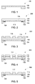
- FIGS. 1-9 are schematic diagrams showing steps of a method of making an electronic package having a conformal masking layer, in accordance with aspects of the present specification.
- FIG. 1 is the schematic representation 100 of a dielectric or dielectric layer 102 of a high density electronic package (not shown in FIG. 1 ) disposed on a processing frame 104.
- the dielectric layer 102 may be made of a polymeric material that is flexible.
- the dielectric layer 102 may be formed of a dielectric material, such as, but not limited to, polyimide or polyimide-based materials.
- the dielectric layer 102 may be made of Kapto ® .
- the dielectric layer 102 may have a thickness of about 25 microns, for example.
- the processing frame 104 may be made of an electrically conductive material, such as aluminum, copper, ceramic-metal composite, nickel, silver, stainless steel, or other suitable materials, or combinations thereof. In one example, the processing frame 104 may be made of Kovar®. Also, the processing frame 104 may or may not form part of the resultant circuit or electronic package.
- a layer (not shown) of an adhesive material may be applied on at least a portion of a first side 108 of the dielectric layer 102.
- a ground layer 109 may be disposed on a second side 110 of the dielectric layer 102.
- the ground layer 109 may be made of an electrically conductive layer.
- the ground layer 109 may be made of copper.
- the ground layer 109 may be a patterned layer.
- another layer of the same or different adhesive may be applied on the ground layer 109 and/or exposed portions of the second side 110 of the dielectric layer 102.
- the adhesive layer may be made of an electrically non-conductive epoxy. It may be noted that the ground layer 109 may be disposed before or after forming the conformal masking layer on the dielectric layer 102.
- a conformal masking layer 112 may be disposed on the first side 108 of the dielectric layer 102.
- the conformal masking layer 112 may be disposed on the adhesive layer.
- the conformal masking layer 112 may be disposed on the adhesive layer after curing of the adhesive layer. The description hereinafter refers to instances where the conformal masking layer 112 is disposed directly on the dielectric layer 102.
- the conformal masking layer 112 may be disposed on the dielectric layer 102 by first disposing a layer 113 of a material of the conformal masking layer 112 on at least a portion of the dielectric layer 102.
- the layer 113 of the material of the conformal masking layer 112 may be processed to form the conformal masking layer 112.
- the layer 113 may be patterned to selectively remove portions of the layer 113 to form the conformal masking layer 112. Further, patterns may be formed in the layer 113 using techniques, such as, but not limited to, lithography, etching, such as laser etching, or both.
- the conformal masking layer 112 may be disposed on both first and second sides 108 and 110 of the dielectric layer 102.
- the layer 113 of the material of the conformal masking layer 112 may be deposited on the portion of the dielectric layer 102 by employing techniques, such as, but not limited to, coating, electroplating, sputtering, spraying, metallization, vapor deposition, pasting, dip coating, or combinations thereof.
- Non-limiting examples of the material of the conformal masking layer 112 may include one or more electrically conductive materials, such as, but not limited to, copper, silver, aluminum, nickel, chrome, titanium, tantalum, or combinations thereof.
- the layer 113 may be transformed to the conformal masking layer 112 (see FIG. 4 ) by patterning the layer 113 to form at least a portion of micro-vias 122 (see FIG. 9 ) in the layer 113 and the dielectric layer 102.
- a resist layer 114 having patterns 116 may be provided.
- the resist layer 114 may be provided on the layer 113 by placing the resist layer 114 on the layer 113, where the resist layer 114 contains the patterns 116.
- the resist layer 114 may be deposited using known deposition techniques, such as spraying, painting, physical vapor deposition, chemical vapor deposition, sputtering, dip coating, or the like. Moreover, the resist layer 114 may include the patterns 116 such that the patterns 116 are similar to the patterns of micro-vias that are intended to be formed in the layer 113 and the dielectric layer 102. In particular, the patterns 116 in the resist layer 114 may correspond to locations and size of the micro-vias 122 that are desirable in a resultant electronic package such as the electronic package 900 (see FIG. 9 ). In one embodiment, the resist layer 114 may be configured to act as a photoresist mask during photolithography to translate the patterns 116 of the resist layer 114 to the layer 113.
- the layer 113 may be patterned with the aid of the resist layer 114, using etching. Accordingly, at least a portion of the layer 113 corresponding to the patterns 116 of the resist layer 114 may be selectively removed to form patterns 117 in the layer 113.
- This layer 113 having the patterns 117 is referred to as the conformal masking layer 112. Further, the patterns 117 constitute a portion of the micro-vias that are formed in the conformal masking layer 112 and the dielectric layer 102.
- the resist layer 114 may be removed. In one example, the resist layer 114 may be removed by dry or wet etching.
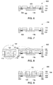
- a semiconductor die 118 having a plurality of contact nodes or pads (not shown) attached or contained within an active surface 120 of the semiconductor die 118 may be coupled or attached to the second side 110 of the dielectric layer 102.
- the semiconductor die 118 may be attached to the portion of the dielectric layer 102 that has the patterns 117.
- the semiconductor die 118 is aligned to the patterns 117 formed in the conformal masking layer 112.
- the semiconductor die 118 may be coupled to the dielectric layer 102 using an adhesive layer disposed between the semiconductor die 118 and the dielectric layer 102.
- FIGS. 6-9 illustrate the semiconductor die 118 as being coupled to the dielectric layer 102
- other electronic components other than the semiconductor die 118, such as active or passive electronic devices, may also be attached to the dielectric layer 102 and/ a portion of the ground layer 109.
- FIGS. 6-9 are explained with respect to a single die, however, the method of the present specification may be extended to couple a plurality of dies, including an array of dies, where one or more dies of the array of dies may be coupled to respective micro-vias in an electronic package.
- a plurality of such electronic components may be attached to the dielectric layer 102 such that a multi-component module or layer may be formed.
- contact pads of the dies may be aligned to the patterns 117, which are representative of positions of future micro-via locations, for electrical connection between the micro-vias and the semiconductor dies.
- the method of the present specification allows the provision for the patterns 117 in the conformal masking layer 112 to be formed before coupling the semiconductor die 118 to the dielectric layer 102. Accordingly, the method facilitates testing of defective or damaged patterns 117 and/or other pre-patterned routing interconnect in the dielectric layer 102.
- the patterns 117 may be tested using visual inspection or automated methods using automatic test equipment and probing devices, as well known to those skilled in the art.
- the patterns 117 may be tested by inspecting the conformal masking layer 112 and a routing layer 136 (see FIG. 9 ). In some embodiments, once the defective or damaged micro-via patterns 117 are identified, the identified defective or damaged patterns 117 micro-via may be exempt from being coupled with the semiconductor dies, such as the semiconductor die 118, thereby saving the expensive semiconductor dies from becoming inoperable due to virtue of them being connected to a faulty micro-via.
- selected portions 121 may be removed.
- the selected portions 121 may be removed to extend the patterns 117 and form the micro-vias 122 (see FIG. 8 ).
- the portions 121 of the dielectric layer 102 may be removed using dry etching, wet etching, ablation, dissolving, drilling, laser ablation, or combinations thereof.
- adhesive layers on one or both sides 108 and 110 of the dielectric layer may be removed.
- patterning beams may be used to remove determined portions of the dielectric layer 102 and adhesive layer (not shown) to form patterns in the dielectric layer 102 that correspond to the patterns 117 (see FIG. 5 ) formed in the conformal masking layer 112. Further, in case of the laser ablation, portions 121 of the dielectric layer 102 may be removed using patterning beams.
- conformal masking layer 112 is configured to define a size of the micro-vias. In particular, the size of the micro-vias may be defined by the patterns 117 formed in the conformal masking layer 112.
- the patterning beams may include laser beams.
- a size of the patterning beams may be greater than or equal to a size of the micro-vias that are to be formed in the dielectric layer 102.
- the size of the patterning beams is larger than the size of the micro-vias 122, presence of the conformal masking layer 112 allows only a portion of the patterning beams corresponding to the desirable size of the micro-vias 122 (see FIG. 8 ) to be incident on the dielectric layer 102.
- the laser ablation may be stopped at the semiconductor die 118 or the adhesive layer disposed between the dielectric layer 102 and the semiconductor die 118 (or at the ground layer 109).
- a thickness of the layer 113 of the material of the conformal masking layer may be such that the layer 113 is configured to withstand energy of the patterning beams without undergoing undesirable disintegration.
- the micro-vias 122 may be blind micro-vias that are configured to provide electrical connections between the semiconductor die 118 and an electronic component, such as a chip, where the semiconductor die 118 and the chip are coupled using the electronic package 900 (see FIG. 9 ). It may be noted that the methods of the present specification enable forming micro-vias, such as the micro-vias 122, which are relatively smaller in size than vias that are typically formed using laser patterning.
- the size of the micro-vias 122 may be even smaller than the size of the patterning beams that are used to form the micro-vias 122.
- the smaller size of the micro-vias 122 is enabled because the material of the conformal masking layer 112 is configured to block at least a portion of the patterning beams, thereby preventing the removal of portions of the dielectric layer 102 disposed under the material of the conformal masking layer 112. Consequently, the size of the micro-vias 122 is determined by the size of the patterns 117 present in the conformal masking layer 112, and not by the size of the patterning beams or laser beams that are used to form selectively remove material of the dielectric layer 102.
- a conformal electrically conductive layer 130 may be deposited on at least a portion of the conformal masking layer 112 as well as at least in the micro-vias 122.
- the conformal electrically conductive layer 130 may be disposed in the micro-vias 122 in a conformal manner.
- Reference numeral 131 refers to an enlarged view of a portion of the electronic package 900 (see FIG. 9 ) to more clearly depict the conformal nature of the conformal electrically conductive layer 130 at least in the micro-vias 122.
- the micro-vias 122 having the conformal electrically conductive layer 130 are referred to as micro-vias 122.
- the conformal electrically conductive layer 130 provides electrical communication between the micro-vias 122 and the semiconductor die 118.
- the conformal electrically conductive layer 130 may include an electrically and thermally conductive material, and according to an exemplary embodiment, may be formed of a metallic material such as copper, silver, or nickel. Further, in one embodiment, the conformal electrically conductive layer 130 may include a single layer or a combination of layers. Moreover, it is also envisioned that composite materials may be used to form the conformal electrically conductive layer 130. In some embodiments, a metal impregnated epoxy or metal-filled paint, may be used as the conformal electrically conductive layer. In some other embodiments, the conformal electrically conductive layer 130 may be deposited using sputtering, electroplating, electro-less plating, or combinations thereof.
- an additional electrical connection layer may be deposited on portions of the semiconductor die 118 corresponding to the micro-vias 122.
- the material for the conformal electrically conductive layer 130 may include titanium, titanium-tungsten, chromium, or combinations thereof.
- additional layers may be deposited as required.
- FIG. 9 is a schematic representation of an electronic package 900.
- selected portions for example, portions at locations 134 of the conformal electrically conductive layer 130 may be removed to form a routing layer 136 on at least a portion of the conformal masking layer 112.
- corresponding portions in the adjacently disposed conformal masking layer 112 may also be removed to isolate traces for routing.
- the routing layer 136 thus formed may include traces that connect micro-vias 122 to other components in the electronic package 900 or the semiconductor die 118 and/or the chip (not shown in FIG. 9 ).
- the conformal masking layer 112 and the routing layer 136 together provide electrical connections between components of the chip and/or the electronic package 900.
- routing layer 136 provides electrical connection between the micro-vias 112 and the conformal masking layer 112.
- the conformal masking layer 112 and the routing layer 136 together form a routing interconnect 138 for the electronic package 900.
- the routing layer 136 may be formed of one or more of titanium, copper, nickel, gold, chrome, aluminum, titanium-tungsten, or combinationds thereof.
- one or more cleaning steps may be introduced after any step that entails removing at least a portion of one or more layers of the electronic package 900.
- a cleaning step may be performed after the step represented by FIG. 3 , where portions of the layer 113 of the material of the conformal masking layer 112 (see FIGS. 6-9 ) are removed.
- a cleaning step or etch step may be performed at least after the steps represented in FIGS. 4, 5 , 7 and 9 are performed. Such cleaning steps may be performed to remove any excess material from a stack of layers that are configured to form the electronic package 900. It may be noted that additional cleaning steps may also be performed.
- a cleaning step may be performed to clean at least a portion of a surface of the conformal masking layer 112 disposed inside the micro-vias 122, outside the micro-vias 122, or both, prior to depositing the conformal electrically conductive layer 130.
- an optional step of cleaning the conformal masking layer 112 may be employed before disposing the conformal electrically conductive layer 130.
- the cleaning step may be used to remove any undesirable material, such as oxides, metals, dielectrics, adhesives to be removed from the surface of the conformal masking layer 112, thereby facilitating enhanced adherence between the conformal masking layer 112 and the conformal electrically conductive layer 130.
- the electronic package 900 may be mounted on an electronic board, for example, a printed circuit board (PCB) using wire bonding, ball grid array, flip-chip assembly, or any other known coupling techniques, or combinations thereof.
- PCB printed circuit board
- wire bonding may be employed for low-cost, simple bonding with relatively larger contact pad size and lower input/output (I/O) density in the electronic package 900.
- electronic pads on the electronic package 900 may be coupled to corresponding electrical traces or electronic pads on the electronic board using an electrically conductive wire to form the wire bond.
- flip-chip technology may be used to electrically couple the electronic package 900 to the electronic board.
- metal bumps, studs, or balls of metals may be applied, for example, in a two dimensional (2D) array pattern, directly to an active surface of the electronic package 900.
- an electrically conductive adhesive may be used to couple the electronic package 900 to an electronic circuit.
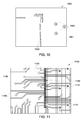
- the portion 1000 includes a conformal masking layer 1001 and micro-vias 1002 that are defined in the conformal masking layer 1001 of the present specification.
- the micro-vias 1002 may be formed using the method illustrated described with respect to FIGS. 1-9 .
- reference numeral 1004 represents conventional micro-vias formed using conventional methods. As illustrated, the micro-vias 1002 are smaller and densely packed in comparison to the conventional vias 1004 that are larger and spaced farther apart from one another. Accordingly, the micro-vias 1002 of the present specification are configured to be coupled to smaller sized dies having a higher density of contact pads.
- FIG. 11 is a top view of a portion of an electronic package 1100 of the present specification.
- the portion 1100 illustrates an array 1102 of micro-vias 1104.
- some of the micro-vias 1104 of the array 1102 may be electrically coupled to other electronic components within or outside the electronic package 1100 using electrical traces 1106 present in a routing layer 1108 of the electronic package 1100.
- the micro-vias 1104 may be electrically coupled to an external electrical device, such as a semiconductor die, using the electrical traces 1106.
- some other micro-vias 1104 may be coupled to other vias 1110, contact pads, or other routing layers on the dielectric layer of the electronic package using routing interconnect 1112.
- the electrical traces 1112 may be used as an electrical interconnect between the external devices to one another or a lower ground plane layer (not shown). These electrical traces 1106 and/or 1112 may be formed in the routing layer 1108 by selectively removing portions of the conformal electrically conductive layer 130 and the conformal masking layer 112, as described with respect to FIGS. 1-9 .
- the electronic package of the present specification serves the purpose of providing an electrical interface between one or more electrical components and a board level circuit component, such as, but not limited to, solder pads on a printed circuit board, contact pads, a socket, or as well known to those of ordinary skill in the art.
- the one or more electrical components may include one or more semiconductor chip dies, also referred to as "dies.”
- the board level circuit component may include a socket or a pad on a printed circuit board.
- the electronic component is configured to provide both a first plurality of electrical connections to the semiconductor die and a second plurality of electrical connections adapted for connection to the board level circuit component.
- the electronic package of the present specification may have a plurality of levels.
- the plurality of levels may include one or more conformal masking layers and/or one or more routing layers and dielectric layers.
- the layers of the plurality of levels may be used to selectively direct signals to and from contact pads of the semiconductor die and/or contact pads or electrical traces of the electronic package.
- a portion of an electronic package 1200 is operatively coupled to a semiconductor die 1202 using semiconductor die pads 1207.
- the electronic package 1200 includes a micro-via 1204.
- the micro-via 1204 includes a well-shaped structure 1212 defined by walls 1211.
- the walls 1211 of the micro-via 1204 extend through an adhesive layer 1206, a dielectric layer 1208 and a combination of a conformal mask layer and a routing interconnect, both represented in a combined fashion by reference numeral 1210.
- the conformal layer on the walls 1211 of the micro-vias 1210 may be operatively coupled to the semiconductor die 1202. It may be noted that the conformal layer on the walls 1211 may be disposed in the entire volume present between the walls 1211. Alternatively, the conformal layer may be disposed in only a portion of the volume defined between the walls 1211 and the semiconductor die 1202.
- the method of making the high density electronic package is illustrated and described with respect to a single die.
- the method may also be used for making an electronic package with a plurality of dies.
- the plurality of dies may be arranged in an array configuration. Further, the plurality of dies may be aligned relative to the positions of the micro-vias using a pick and place robotic device and one or more fiducial reference points. Further, in some embodiments, the method may also be used for making a plurality of electronic packages per processing frame. In these embodiments, each electronic package may have one or more semiconductor dies.
- FIG. 13 represents an exemplary electronic package 1300 having a plurality of semiconductor dies 1302 coupled to a dielectric layer 1304. Further, the electronic package 1300 includes a conformal masking layer 1306 and a routing layer 1308. Also, the conformal masking layer 1306 and the routing layer 1308 together form a routing interconnect 1314 for the electronic package 1300. Moreover, a plurality of micro-vias 1310 is disposed in at least a portion of the conformal masking layer 1306 and the routing layer 1308. Portions of the routing layer 1308 form an electrically conductive layer in the plurality of micro-vias 1310 to provide electrical connection between the micro-vias 1310 and the plurality of semiconductor dies 1302.
- the plurality of semiconductor dies 1302 may be arranged on the dielectric layer 1304 such that electrical connections, such as contact pads, on each of the semiconductor dies 1302 are aligned with corresponding micro-vias 1310 of the plurality of micro-vias 1310. Moreover, although not illustrated, some of the micro-vias 1310 of the plurality of micro-vias 1310 may be exempted from being coupled to the semiconductor dies 1302 or any other electrical devices. By way of example, upon inspection if it is determined that certain micro-vias 1310 are defective, the defective micro-vias 134 may not be coupled to the semiconductor dies 1302. Further, in the illustrated embodiment, the electronic package 1300 may be formed on a common processing frame (not shown).
- the electronic package 1300 may include a plurality of such processing frames. Further, in these embodiments, each of the plurality of processing frames may include one or more semiconductor dies. It may be noted that a stacked structure comprising a plurality of electronic packages, such as electronic package 900, electronic package 1300, or the like, and methods of making the same are envisioned within the scope of the present specification.
- the electronic package of the present specification is configured to provide routing between at least one or more electrical components while accommodating space limitations, reduced pitches and increased routing density.
- having micro-vias that have an average diameter in a range from about 5 microns to about 50 microns and pitch in a range from about 10 microns to about 100 microns enables operatively coupling smaller circuit boards that may require higher routing density.
Landscapes
- Production Of Multi-Layered Print Wiring Board (AREA)
- Printing Elements For Providing Electric Connections Between Printed Circuits (AREA)
- Internal Circuitry In Semiconductor Integrated Circuit Devices (AREA)
- Physics & Mathematics (AREA)
- Geometry (AREA)
Abstract
Description
- This invention was made with Government support under grant number FA9453-09-C-0305 awarded by the Air Force Research Laboratories. The Government has certain rights in the invention.
- Embodiments of the present specification relate to electronic packages, and more particularly, forming micro-vias and interconnects in the electronic packages.
- Technological advancements in the area of electronic devices have experienced vast growth in recent years. For example, while cellular phones are becoming smaller and lighter, their features and capabilities are simultaneously expanding. This has caused an increase in the complexity and operation of the electrical components found in such devices and a decrease in the amount of space available for such components. Several challenges arise from such an increase in the complexity of the electrical components and decrease in the amount of space available. For example, based on space limitations, circuit boards are reduced in size to an extent that the routing density for the board may be constrained and limited below a desired amount. As integrated circuits become increasingly smaller and yield better operating performance, packaging technology for integrated circuit (IC) packaging has correspondingly evolved from leaded packaging to laminate-based ball grid array (BGA) packaging and eventually to chip scale packaging (CSP). Advancements in IC chip packaging technology are driven by ever-increasing needs for achieving better performance, greater miniaturization, and higher reliability. New packaging technology has to further provide for the possibilities of batch production for the purpose of large-scale manufacturing thereby allowing economy of scale.
- Furthermore, due to the small size and complexity of IC packages, the process for fabricating the IC packages is typically expensive and time consuming. Also, use of additional re-distribution layers to create desired double-sided input/output (I/O) system increases the number of processing steps, further increasing the cost and complexity of the manufacturing process. Moreover, increasing I/O per device increases routing density and number of vias that are required per device.
- In accordance with aspects of the present specification, an electronic package is presented. The electronic package includes a dielectric layer and a conformal masking layer disposed on at least a portion of the dielectric layer. The electronic package further includes a routing layer disposed on at least a portion of the conformal masking layer and a micro-via disposed at least in part in the conformal masking layer and the routing layer. Further, at least a portion of the routing layer forms a conformal electrically conductive layer in at least a portion of the micro-via. Also, the conformal masking layer is configured to define a size of the micro-via. The electronic package further includes a semiconductor die operatively coupled to the micro-via.
- In accordance with another aspect of the present specification, an electronic system having an electronic package is presented. The electronic package includes a dielectric layer, a conformal masking layer disposed on at least a portion of the dielectric layer, and a routing layer disposed on at least a portion of the conformal masking layer. Further, the electronic package includes a plurality of micro-vias disposed at least in part in the conformal masking layer and the routing layer. Moreover, at least a portion of the routing layer forms a conformal electrically conductive layer in at least a portion of micro-vias of the plurality of micro-vias. The electronic system further includes a plurality of semiconductor dies, where one or more semiconductor dies of the plurality of semiconductor dies are coupled to corresponding micro-vias of the plurality of micro-vias.
- In accordance with yet another aspect of the present specification, a method of making an electronic package is included. The method includes providing a dielectric layer disposed on a processing frame, where the dielectric layer includes a first side and a second side. Further, the method includes providing a conformal masking layer disposed on the second side of the dielectric layer, where the conformal masking layer includes one or more patterns corresponding to one or more micro-vias. Moreover, the method includes coupling a semiconductor die to a portion of the first side of the dielectric layer such that the semiconductor die is aligned with the one or more patterns. Also, the method includes selectively removing portions of the dielectric layer corresponding to the one or more patterns in the conformal masking layer. In addition, the method includes disposing a conformal electrically conductive layer in at least a portion of one or more patterns corresponding to the one or more micro-vias to form the one or more micro-vias, where the conformal masking layer is configured to define a size of the one or more micro-vias. Moreover, the method includes selectively removing portions of the dielectric layer to form the one or more microvias.
- These and other features, aspects, and advantages of the present disclosure will become better understood when the following detailed description is read with reference to the accompanying drawings in which like characters represent like parts throughout the drawings, wherein:
-
FIGS. 1-9 are schematic representations of steps involved in an exemplary method of making an electronic package having a micro-via, in accordance with aspects of the present specification; -
FIG. 10 is a top view of micro-vias employed in an electronic package, where the micro-vias are fabricated using the method represented inFIGS. 1-9 , in accordance with aspects of the present specification; -
FIG. 11 is a top view of electrical routing in the electronic package ofFIG. 10 , in accordance with aspects of the present specification; -
FIG. 12 is a cross-sectional view of a portion of an exemplary electronic package having a micro-via, in accordance with aspects of the present specification; and -
FIG. 13 is a cross-sectional view of a portion of an electronic system having a plurality of dies, in accordance with aspects of the present specification. - Embodiments of the present specification relate to electronic packages having conformal masking layers and methods of making the same. In certain embodiments, at least a portion of a conformal masking layer of an electronic package conforms to at least a portion of one or more micro-vias present in the electronic package. Further, the conformal masking layer may be made of an electrically conductive material and configured to form a part of an electronic circuit or a thermal pathway in the electronic package. Once the conformal masking layer defines the via size the conformal masking layer may be integrated into the electronic package to form other structures. By way of example, the conformal masking layer may be configured to act as a ground plane, power source, signal source, shield layer, or combinations thereof. In instances where the conformal masking layer is configured to act as the shield layer, the conformal masking layer may be configured to provide a localized shield against at least a portion of radio frequency and/or electromagnetic radiation.
- In certain embodiments, the electronic package may be used to couple one or more semiconductor devices (such as semiconductor dies) to one or more electronic components. In one example, the electronic package may be easily coupled to a printed circuit board (PCB) for providing electrical connection between the printed circuit board and other electronic components. In one embodiment, the electronic package may be used to provide high density electrical connections by virtue of small size and pitch of the micro-vias. In certain embodiments, an average diameter of the micro-vias may be in a range from about 5 microns to about 50 microns. In certain other embodiments, an average diameter of the micro-vias may be in a range from about 5 microns to about 25 microns, or from about 10 microns to about 50 microns. Further, in some embodiments, an average pitch between two adjacently disposed micro-vias may be in a range from about 10 microns to about 100 microns. Further, in one embodiment, the micro-vias may be through micro-vias or blind micro-vias. As used herein, the term "through micro-vias" is used to refer to micro-vias that go through a layer and do not have a bottom end. Moreover, as used herein, the term "blind micro-vias" is used to refer to micro-vias that have a bottom end that is in electrical contact with an adjacently disposed or underlying layer or an integrated circuit (IC) pad. In one embodiment, the micro-vias may not have any wall or layer disposed between a corresponding pad of the semiconductor device and the micro-vias. In some embodiments, the micro-vias may be arranged in a linear arrangement, an array, or any other geometrical or non-geometrical arrangement. In certain embodiments, an electronic package employing the micro-vias may be compatible with conventional die bonding techniques, such as, but not limited to, wire bonding, flip-chip technology, and other methods of connecting electronic input/output (I/O) pads of a semiconductor die to the electronic package.
-
FIGS. 1-9 are schematic diagrams showing steps of a method of making an electronic package having a conformal masking layer, in accordance with aspects of the present specification.FIG. 1 is theschematic representation 100 of a dielectric ordielectric layer 102 of a high density electronic package (not shown inFIG. 1 ) disposed on aprocessing frame 104. Further, in some embodiments, thedielectric layer 102 may be made of a polymeric material that is flexible. In one embodiment, thedielectric layer 102 may be formed of a dielectric material, such as, but not limited to, polyimide or polyimide-based materials. In a particular example, thedielectric layer 102 may be made of Kapto®. In certain embodiments, thedielectric layer 102 may have a thickness of about 25 microns, for example. Further, theprocessing frame 104 may be made of an electrically conductive material, such as aluminum, copper, ceramic-metal composite, nickel, silver, stainless steel, or other suitable materials, or combinations thereof. In one example, theprocessing frame 104 may be made of Kovar®. Also, theprocessing frame 104 may or may not form part of the resultant circuit or electronic package. - Optionally, as illustrated in the
schematic representation 200 ofFIG. 2 , a layer (not shown) of an adhesive material may be applied on at least a portion of afirst side 108 of thedielectric layer 102. Also, aground layer 109 may be disposed on asecond side 110 of thedielectric layer 102. Theground layer 109 may be made of an electrically conductive layer. In a non-limiting example, theground layer 109 may be made of copper. Further, theground layer 109 may be a patterned layer. Moreover, in some embodiments, another layer of the same or different adhesive may be applied on theground layer 109 and/or exposed portions of thesecond side 110 of thedielectric layer 102. In one example, the adhesive layer may be made of an electrically non-conductive epoxy. It may be noted that theground layer 109 may be disposed before or after forming the conformal masking layer on thedielectric layer 102. - Additionally, a conformal masking layer 112 (see
FIG. 4 ) may be disposed on thefirst side 108 of thedielectric layer 102. Alternatively, in instances where the adhesive layer is disposed on thedielectric layer 102, theconformal masking layer 112 may be disposed on the adhesive layer. Further, theconformal masking layer 112 may be disposed on the adhesive layer after curing of the adhesive layer. The description hereinafter refers to instances where theconformal masking layer 112 is disposed directly on thedielectric layer 102. In certain embodiments, theconformal masking layer 112 may be disposed on thedielectric layer 102 by first disposing alayer 113 of a material of theconformal masking layer 112 on at least a portion of thedielectric layer 102. Subsequently, thelayer 113 of the material of theconformal masking layer 112 may be processed to form theconformal masking layer 112. In one example, thelayer 113 may be patterned to selectively remove portions of thelayer 113 to form theconformal masking layer 112. Further, patterns may be formed in thelayer 113 using techniques, such as, but not limited to, lithography, etching, such as laser etching, or both. Although not illustrated, it may be noted that theconformal masking layer 112 may be disposed on both first andsecond sides dielectric layer 102. In certain embodiments, thelayer 113 of the material of theconformal masking layer 112 may be deposited on the portion of thedielectric layer 102 by employing techniques, such as, but not limited to, coating, electroplating, sputtering, spraying, metallization, vapor deposition, pasting, dip coating, or combinations thereof. Non-limiting examples of the material of theconformal masking layer 112 may include one or more electrically conductive materials, such as, but not limited to, copper, silver, aluminum, nickel, chrome, titanium, tantalum, or combinations thereof. - Referring now to the
schematic representation 300 ofFIG. 3 , thelayer 113 may be transformed to the conformal masking layer 112 (seeFIG. 4 ) by patterning thelayer 113 to form at least a portion of micro-vias 122 (seeFIG. 9 ) in thelayer 113 and thedielectric layer 102. To form the patterns corresponding to the micro-vias 122 in thelayer 113, a resistlayer 114 havingpatterns 116 may be provided. In one embodiment, the resistlayer 114 may be provided on thelayer 113 by placing the resistlayer 114 on thelayer 113, where the resistlayer 114 contains thepatterns 116. Further, the resistlayer 114 may be deposited using known deposition techniques, such as spraying, painting, physical vapor deposition, chemical vapor deposition, sputtering, dip coating, or the like. Moreover, the resistlayer 114 may include thepatterns 116 such that thepatterns 116 are similar to the patterns of micro-vias that are intended to be formed in thelayer 113 and thedielectric layer 102. In particular, thepatterns 116 in the resistlayer 114 may correspond to locations and size of the micro-vias 122 that are desirable in a resultant electronic package such as the electronic package 900 (seeFIG. 9 ). In one embodiment, the resistlayer 114 may be configured to act as a photoresist mask during photolithography to translate thepatterns 116 of the resistlayer 114 to thelayer 113. - Next, as illustrated in the
schematic representation 400 ofFIG. 4 , thelayer 113 may be patterned with the aid of the resistlayer 114, using etching. Accordingly, at least a portion of thelayer 113 corresponding to thepatterns 116 of the resistlayer 114 may be selectively removed to formpatterns 117 in thelayer 113. Thislayer 113 having thepatterns 117 is referred to as theconformal masking layer 112. Further, thepatterns 117 constitute a portion of the micro-vias that are formed in theconformal masking layer 112 and thedielectric layer 102. Moreover, as illustrated in theschematic representation 500 ofFIG. 5 , after forming thepatterns 117 in thelayer 113, the resistlayer 114 may be removed. In one example, the resistlayer 114 may be removed by dry or wet etching. - Additionally, as illustrated in the
schematic representation 600 ofFIG. 6 , asemiconductor die 118 having a plurality of contact nodes or pads (not shown) attached or contained within anactive surface 120 of the semiconductor die 118 may be coupled or attached to thesecond side 110 of thedielectric layer 102. In particular, the semiconductor die 118 may be attached to the portion of thedielectric layer 102 that has thepatterns 117. By way of example, as illustrated inFIG. 6 , the semiconductor die 118 is aligned to thepatterns 117 formed in theconformal masking layer 112. In some embodiments, the semiconductor die 118 may be coupled to thedielectric layer 102 using an adhesive layer disposed between the semiconductor die 118 and thedielectric layer 102. - While
FIGS. 6-9 illustrate the semiconductor die 118 as being coupled to thedielectric layer 102, it is envisioned that other electronic components other than the semiconductor die 118, such as active or passive electronic devices, may also be attached to thedielectric layer 102 and/ a portion of theground layer 109. Further, althoughFIGS. 6-9 are explained with respect to a single die, however, the method of the present specification may be extended to couple a plurality of dies, including an array of dies, where one or more dies of the array of dies may be coupled to respective micro-vias in an electronic package. Accordingly, although not illustrated, it is contemplated that a plurality of such electronic components may be attached to thedielectric layer 102 such that a multi-component module or layer may be formed. Further, in embodiments where a plurality of dies is employed, contact pads of the dies may be aligned to thepatterns 117, which are representative of positions of future micro-via locations, for electrical connection between the micro-vias and the semiconductor dies. - It may be appreciated that as the cost and complexity of semiconductor dies, such as application specific integrated circuit chips (ASICs), increases, there is a corresponding increase in the cost of designing, qualifying and fabricating packaging for these devices. Advantageously, the method of the present specification allows the provision for the
patterns 117 in theconformal masking layer 112 to be formed before coupling the semiconductor die 118 to thedielectric layer 102. Accordingly, the method facilitates testing of defective or damagedpatterns 117 and/or other pre-patterned routing interconnect in thedielectric layer 102. In one embodiment, thepatterns 117 may be tested using visual inspection or automated methods using automatic test equipment and probing devices, as well known to those skilled in the art. In one example, thepatterns 117 may be tested by inspecting theconformal masking layer 112 and a routing layer 136 (seeFIG. 9 ). In some embodiments, once the defective or damagedmicro-via patterns 117 are identified, the identified defective or damagedpatterns 117 micro-via may be exempt from being coupled with the semiconductor dies, such as the semiconductor die 118, thereby saving the expensive semiconductor dies from becoming inoperable due to virtue of them being connected to a faulty micro-via. - Further, as illustrated in the schematic representation of
FIG. 7 , after coupling the semiconductor die 118 to thesecond side 110 of thedielectric layer 102, selected portions 121 (seeFIG. 6 ) of thedielectric layer 102 may be removed. In particular, the selectedportions 121 may be removed to extend thepatterns 117 and form the micro-vias 122 (seeFIG. 8 ). In one embodiment, theportions 121 of thedielectric layer 102 may be removed using dry etching, wet etching, ablation, dissolving, drilling, laser ablation, or combinations thereof. Further, it may be noted that along with the selectedportions 121 of thedielectric layer 102 adhesive layers on one or bothsides - In case of laser ablation of the
dielectric layer 102, patterning beams (not shown inFIG. 7 ) may be used to remove determined portions of thedielectric layer 102 and adhesive layer (not shown) to form patterns in thedielectric layer 102 that correspond to the patterns 117 (seeFIG. 5 ) formed in theconformal masking layer 112. Further, in case of the laser ablation,portions 121 of thedielectric layer 102 may be removed using patterning beams. It may be noted thatconformal masking layer 112 is configured to define a size of the micro-vias. In particular, the size of the micro-vias may be defined by thepatterns 117 formed in theconformal masking layer 112. In one embodiment, the patterning beams may include laser beams. In an exemplary embodiment, a size of the patterning beams may be greater than or equal to a size of the micro-vias that are to be formed in thedielectric layer 102. In embodiments where the size of the patterning beams is larger than the size of the micro-vias 122, presence of theconformal masking layer 112 allows only a portion of the patterning beams corresponding to the desirable size of the micro-vias 122 (seeFIG. 8 ) to be incident on thedielectric layer 102. Further, oncepatterns 121 that correspond to thepatterns 117 in thelayer 112 are formed the laser ablation may be stopped at the semiconductor die 118 or the adhesive layer disposed between thedielectric layer 102 and the semiconductor die 118 (or at the ground layer 109). In one embodiment, a thickness of thelayer 113 of the material of the conformal masking layer may be such that thelayer 113 is configured to withstand energy of the patterning beams without undergoing undesirable disintegration. In certain embodiments, the micro-vias 122 may be blind micro-vias that are configured to provide electrical connections between the semiconductor die 118 and an electronic component, such as a chip, where the semiconductor die 118 and the chip are coupled using the electronic package 900 (seeFIG. 9 ). It may be noted that the methods of the present specification enable forming micro-vias, such as the micro-vias 122, which are relatively smaller in size than vias that are typically formed using laser patterning. In particular, the size of the micro-vias 122 may be even smaller than the size of the patterning beams that are used to form the micro-vias 122. Advantageously, the smaller size of the micro-vias 122 is enabled because the material of theconformal masking layer 112 is configured to block at least a portion of the patterning beams, thereby preventing the removal of portions of thedielectric layer 102 disposed under the material of theconformal masking layer 112. Consequently, the size of the micro-vias 122 is determined by the size of thepatterns 117 present in theconformal masking layer 112, and not by the size of the patterning beams or laser beams that are used to form selectively remove material of thedielectric layer 102. - Also, as illustrated in the
schematic representation 800 ofFIG. 8 , a conformal electricallyconductive layer 130 may be deposited on at least a portion of theconformal masking layer 112 as well as at least in the micro-vias 122. The conformal electricallyconductive layer 130 may be disposed in the micro-vias 122 in a conformal manner.Reference numeral 131 refers to an enlarged view of a portion of the electronic package 900 (seeFIG. 9 ) to more clearly depict the conformal nature of the conformal electricallyconductive layer 130 at least in the micro-vias 122. The micro-vias 122 having the conformal electricallyconductive layer 130 are referred to asmicro-vias 122. Further, the conformal electricallyconductive layer 130 provides electrical communication between the micro-vias 122 and the semiconductor die 118. The conformal electricallyconductive layer 130 may include an electrically and thermally conductive material, and according to an exemplary embodiment, may be formed of a metallic material such as copper, silver, or nickel. Further, in one embodiment, the conformal electricallyconductive layer 130 may include a single layer or a combination of layers. Moreover, it is also envisioned that composite materials may be used to form the conformal electricallyconductive layer 130. In some embodiments, a metal impregnated epoxy or metal-filled paint, may be used as the conformal electrically conductive layer. In some other embodiments, the conformal electricallyconductive layer 130 may be deposited using sputtering, electroplating, electro-less plating, or combinations thereof. - Optionally, in some embodiments, before depositing the conformal electrically
conductive layer 130, an additional electrical connection layer may be deposited on portions of the semiconductor die 118 corresponding to the micro-vias 122. Non-limiting examples of the material for the conformal electricallyconductive layer 130 may include titanium, titanium-tungsten, chromium, or combinations thereof. Further, in same or different embodiments, in addition to the conformal electricallyconductive layer 130, additional layers may be deposited as required. -
FIG. 9 is a schematic representation of anelectronic package 900. As illustrated inFIG. 9 , selected portions, for example, portions atlocations 134 of the conformal electricallyconductive layer 130 may be removed to form arouting layer 136 on at least a portion of theconformal masking layer 112. Furthermore, corresponding portions in the adjacently disposedconformal masking layer 112 may also be removed to isolate traces for routing. Therouting layer 136 thus formed may include traces that connect micro-vias 122 to other components in theelectronic package 900 or the semiconductor die 118 and/or the chip (not shown inFIG. 9 ). Theconformal masking layer 112 and therouting layer 136 together provide electrical connections between components of the chip and/or theelectronic package 900. It may be noted that therouting layer 136 provides electrical connection between the micro-vias 112 and theconformal masking layer 112. Theconformal masking layer 112 and therouting layer 136 together form arouting interconnect 138 for theelectronic package 900. Further, therouting layer 136 may be formed of one or more of titanium, copper, nickel, gold, chrome, aluminum, titanium-tungsten, or combinationds thereof. - Further, one or more cleaning steps may be introduced after any step that entails removing at least a portion of one or more layers of the
electronic package 900. By way of example, a cleaning step may be performed after the step represented byFIG. 3 , where portions of thelayer 113 of the material of the conformal masking layer 112 (seeFIGS. 6-9 ) are removed. Similarly, a cleaning step or etch step may be performed at least after the steps represented inFIGS. 4, 5 ,7 and 9 are performed. Such cleaning steps may be performed to remove any excess material from a stack of layers that are configured to form theelectronic package 900. It may be noted that additional cleaning steps may also be performed. By way of example, a cleaning step may be performed to clean at least a portion of a surface of theconformal masking layer 112 disposed inside the micro-vias 122, outside the micro-vias 122, or both, prior to depositing the conformal electricallyconductive layer 130. In some embodiments, an optional step of cleaning theconformal masking layer 112 may be employed before disposing the conformal electricallyconductive layer 130. In one example, the cleaning step may be used to remove any undesirable material, such as oxides, metals, dielectrics, adhesives to be removed from the surface of theconformal masking layer 112, thereby facilitating enhanced adherence between theconformal masking layer 112 and the conformal electricallyconductive layer 130. - In certain embodiments, the electronic package 900 (see
FIG. 9 ) may be mounted on an electronic board, for example, a printed circuit board (PCB) using wire bonding, ball grid array, flip-chip assembly, or any other known coupling techniques, or combinations thereof. By way of example, for low-cost, simple bonding with relatively larger contact pad size and lower input/output (I/O) density in theelectronic package 900, wire bonding may be employed. Further, electronic pads on theelectronic package 900 may be coupled to corresponding electrical traces or electronic pads on the electronic board using an electrically conductive wire to form the wire bond. - In another example, for low-cost, relatively high I/O density in the semiconductor die 118 or the
electronic package 900, flip-chip technology may be used to electrically couple theelectronic package 900 to the electronic board. Further, in some embodiments, metal bumps, studs, or balls of metals (collectively referred to herein as "bump-type" interconnections) may be applied, for example, in a two dimensional (2D) array pattern, directly to an active surface of theelectronic package 900. Alternatively, in one embodiment, an electrically conductive adhesive may be used to couple theelectronic package 900 to an electronic circuit. - Turning now to
FIG. 10 , a top view of aportion 1000 of an electronic package of the present specification is illustrated. Theportion 1000 includes aconformal masking layer 1001 and micro-vias 1002 that are defined in theconformal masking layer 1001 of the present specification. The micro-vias 1002 may be formed using the method illustrated described with respect toFIGS. 1-9 . Further,reference numeral 1004 represents conventional micro-vias formed using conventional methods. As illustrated, the micro-vias 1002 are smaller and densely packed in comparison to theconventional vias 1004 that are larger and spaced farther apart from one another. Accordingly, the micro-vias 1002 of the present specification are configured to be coupled to smaller sized dies having a higher density of contact pads. -
FIG. 11 is a top view of a portion of anelectronic package 1100 of the present specification. In the illustrated embodiment, theportion 1100 illustrates anarray 1102 of micro-vias 1104. Further, some of the micro-vias 1104 of thearray 1102 may be electrically coupled to other electronic components within or outside theelectronic package 1100 usingelectrical traces 1106 present in arouting layer 1108 of theelectronic package 1100. By way of example, the micro-vias 1104 may be electrically coupled to an external electrical device, such as a semiconductor die, using theelectrical traces 1106. Also, some other micro-vias 1104 may be coupled toother vias 1110, contact pads, or other routing layers on the dielectric layer of the electronic package usingrouting interconnect 1112. Also, theelectrical traces 1112 may be used as an electrical interconnect between the external devices to one another or a lower ground plane layer (not shown). Theseelectrical traces 1106 and/or 1112 may be formed in therouting layer 1108 by selectively removing portions of the conformal electricallyconductive layer 130 and theconformal masking layer 112, as described with respect toFIGS. 1-9 . - In some embodiments, the electronic package of the present specification serves the purpose of providing an electrical interface between one or more electrical components and a board level circuit component, such as, but not limited to, solder pads on a printed circuit board, contact pads, a socket, or as well known to those of ordinary skill in the art. In a non-limiting example, the one or more electrical components may include one or more semiconductor chip dies, also referred to as "dies." Further, the board level circuit component may include a socket or a pad on a printed circuit board. Moreover, the electronic component is configured to provide both a first plurality of electrical connections to the semiconductor die and a second plurality of electrical connections adapted for connection to the board level circuit component.
- In certain embodiments, the electronic package of the present specification may have a plurality of levels. In one example, the plurality of levels may include one or more conformal masking layers and/or one or more routing layers and dielectric layers. The layers of the plurality of levels may be used to selectively direct signals to and from contact pads of the semiconductor die and/or contact pads or electrical traces of the electronic package.
- Referring to the schematic representation of
FIG. 12 , a portion of anelectronic package 1200 is operatively coupled to asemiconductor die 1202 usingsemiconductor die pads 1207. Theelectronic package 1200 includes amicro-via 1204. Further, themicro-via 1204 includes a well-shapedstructure 1212 defined bywalls 1211. Moreover, thewalls 1211 of the micro-via 1204 extend through anadhesive layer 1206, adielectric layer 1208 and a combination of a conformal mask layer and a routing interconnect, both represented in a combined fashion byreference numeral 1210. The conformal layer on thewalls 1211 of the micro-vias 1210 may be operatively coupled to thesemiconductor die 1202. It may be noted that the conformal layer on thewalls 1211 may be disposed in the entire volume present between thewalls 1211. Alternatively, the conformal layer may be disposed in only a portion of the volume defined between thewalls 1211 and thesemiconductor die 1202. - Further, it may be noted that the method of making the high density electronic package is illustrated and described with respect to a single die. However, the method may also be used for making an electronic package with a plurality of dies. In one embodiment, the plurality of dies may be arranged in an array configuration. Further, the plurality of dies may be aligned relative to the positions of the micro-vias using a pick and place robotic device and one or more fiducial reference points. Further, in some embodiments, the method may also be used for making a plurality of electronic packages per processing frame. In these embodiments, each electronic package may have one or more semiconductor dies.
-
FIG. 13 represents an exemplaryelectronic package 1300 having a plurality of semiconductor dies 1302 coupled to adielectric layer 1304. Further, theelectronic package 1300 includes aconformal masking layer 1306 and arouting layer 1308. Also, theconformal masking layer 1306 and therouting layer 1308 together form arouting interconnect 1314 for theelectronic package 1300. Moreover, a plurality of micro-vias 1310 is disposed in at least a portion of theconformal masking layer 1306 and therouting layer 1308. Portions of therouting layer 1308 form an electrically conductive layer in the plurality of micro-vias 1310 to provide electrical connection between the micro-vias 1310 and the plurality of semiconductor dies 1302. Further, the plurality of semiconductor dies 1302 may be arranged on thedielectric layer 1304 such that electrical connections, such as contact pads, on each of the semiconductor dies 1302 are aligned with corresponding micro-vias 1310 of the plurality of micro-vias 1310. Moreover, although not illustrated, some of the micro-vias 1310 of the plurality of micro-vias 1310 may be exempted from being coupled to the semiconductor dies 1302 or any other electrical devices. By way of example, upon inspection if it is determined that certain micro-vias 1310 are defective, the defective micro-vias 134 may not be coupled to the semiconductor dies 1302. Further, in the illustrated embodiment, theelectronic package 1300 may be formed on a common processing frame (not shown). However, in some other embodiments, theelectronic package 1300 may include a plurality of such processing frames. Further, in these embodiments, each of the plurality of processing frames may include one or more semiconductor dies. It may be noted that a stacked structure comprising a plurality of electronic packages, such aselectronic package 900,electronic package 1300, or the like, and methods of making the same are envisioned within the scope of the present specification. - Advantageously, the electronic package of the present specification is configured to provide routing between at least one or more electrical components while accommodating space limitations, reduced pitches and increased routing density. By way of example, having micro-vias that have an average diameter in a range from about 5 microns to about 50 microns and pitch in a range from about 10 microns to about 100 microns, enables operatively coupling smaller circuit boards that may require higher routing density.
- While only certain features of the disclosure have been illustrated and described herein, many modifications and changes will occur to those skilled in the art. It is, therefore, to be understood that the appended claims are intended to cover all such modifications and changes as fall within the true spirit of the disclosure.
Claims (15)
- An electronic package, comprising:a dielectric layer (102);a conformal masking layer (112) disposed on at least a portion of the dielectric layer (102);a routing layer (136) disposed on at least a portion of the conformal masking layer (112);a micro-via (122) disposed at least in part in the conformal masking layer (112) and the routing layer (136), wherein at least a portion of the routing layer (136) forms a conformal electrically conductive layer (130) in at least a portion of the micro-via (122), and wherein the conformal masking layer (112) s configured to define a size of the micro-via (122); anda semiconductor (118) die coupled to the micro-via (122).
- The electronic package of claim 1, wherein the conformal masking layer (112) comprises an electrically conductive material.
- The electronic package of claim 2, wherein the electrically conductive material includes, copper, titanium, aluminum, nickel, gold, tungsten chrome tantelum, or combinations thereof.
- The electronic package of any of claims 1 to 3, wherein at least a portion of the micro-via (122) is disposed in the conformal masking layer (112), the routing layer (136), and the dielectric layer (102).
- The electronic package of any preceding claim, wherein the micro-via is a blind micro-via (122).
- The electronic package of any preceding claim, wherein a diameter of the micro-via is in a range from about 5 microns to about 50 microns.
- The electronic package of any preceding claim, wherein the routing layer (136) is configured to be deposited on the conformal masking layer (112).
- The electronic package of any preceding claim, wherein the routing layer (136) comprises titanium, copper, nickel, gold, chrome, aluminum, titanium-tungsten, or combinations thereof.
- The electronic package of any preceding claim, wherein the conformal masking layer (112) and the routing layer (136) form a routing interconnect (138).
- An electronic package of any preceding claim, further comprising:a plurality of micro-vias (122) disposed at least in part in the conformal masking layer (112) and the routing layer (136), wherein at least a portion of the routing layer (136) forms a conformal electrically conductive layer (130) in at least a portion of micro-vias (122) of the plurality of micro-vias; anda plurality of semiconductor dies (118), wherein one or more semiconductor dies of the plurality of semiconductor dies are coupled to corresponding micro-vias (122) of the plurality of micro-vias (122).
- A method of making an electronic package, comprising:providing a dielectric layer (102) disposed on a processing frame (104), wherein the dielectric layer (102) comprises a first side (108) and a second side (110);providing a conformal masking layer (112) disposed on the second side (110) of the dielectric layer (102), wherein the conformal masking layer (112) comprises one or more patterns (117) corresponding to one or more micro-vias (122);coupling a semiconductor die (118) to a portion of the first side (108) of the dielectric layer (102) such that the semiconductor die (118) is aligned with the one or more patterns (117);selectively removing portions of the dielectric layer (102); anddisposing a conformal electrically conductive layer (130) in at least a portion of the one or more patterns (117) corresponding to the one or more micro-vias (122) to form the one or more micro-vias (122), wherein the conformal masking layer (136) is configured to define a size of the one or more micro-vias (122).
- The method of claim 11 wherein the step of providing the conformal masking layer (112) comprises:disposing a layer of material (113) of the conformal masking layer (112) on at least a portion of the second side (110) of the dielectric layer (102); andpatterning the layer of the material (113) of the conformal masking layer (112) to form the conformal masking layer (112).
- The method of claim 11 or 12, further comprising:disposing a patterned resist layer (114) on at least a portion of the layer of the material (113) of the conformal masking layer (112); andremoving exposed portions of the layer of the material (113) of the conformal masking layer (112) corresponding to the one or more patterns (117) Pof the one or more micro-vias (122).
- The method of any of claims 11 to 13, wherein selectively removing the portions of the dielectric layer (102) comprises laser drilling the portions of the dielectric layer (102).
- The method of claim 14, further comprising removing the resist layer (114).
Applications Claiming Priority (1)
| Application Number | Priority Date | Filing Date | Title |
|---|---|---|---|
| US14/556,258 US9666516B2 (en) | 2014-12-01 | 2014-12-01 | Electronic packages and methods of making and using the same |
Publications (1)
| Publication Number | Publication Date |
|---|---|
| EP3029719A1 true EP3029719A1 (en) | 2016-06-08 |
Family
ID=54704997
Family Applications (1)
| Application Number | Title | Priority Date | Filing Date |
|---|---|---|---|
| EP15195705.7A Pending EP3029719A1 (en) | 2014-12-01 | 2015-11-20 | Electronic packages and methods of making and using the same |
Country Status (6)
| Country | Link |
|---|---|
| US (1) | US9666516B2 (en) |
| EP (1) | EP3029719A1 (en) |
| JP (1) | JP2016111350A (en) |
| KR (1) | KR101786226B1 (en) |
| CN (1) | CN105655321A (en) |
| TW (1) | TWI596738B (en) |
Families Citing this family (5)
| Publication number | Priority date | Publication date | Assignee | Title |
|---|---|---|---|---|
| AT513747B1 (en) * | 2013-02-28 | 2014-07-15 | Mikroelektronik Ges Mit Beschränkter Haftung Ab | Assembly process for circuit carriers and circuit carriers |
| US10497648B2 (en) * | 2018-04-03 | 2019-12-03 | General Electric Company | Embedded electronics package with multi-thickness interconnect structure and method of making same |
| US11398445B2 (en) * | 2020-05-29 | 2022-07-26 | General Electric Company | Mechanical punched via formation in electronics package and electronics package formed thereby |
| US11705365B2 (en) * | 2021-05-18 | 2023-07-18 | Applied Materials, Inc. | Methods of micro-via formation for advanced packaging |
| CN115995423B (en) * | 2023-01-06 | 2025-11-21 | 长鑫存储技术有限公司 | Semiconductor structure and forming method thereof, stacking structure and forming method thereof |
Citations (2)
| Publication number | Priority date | Publication date | Assignee | Title |
|---|---|---|---|---|
| US20080032447A1 (en) * | 2006-08-04 | 2008-02-07 | Micron Technology, Inc. | Microelectronic devices and methods for manufacturing microelectronic devices |
| US8114712B1 (en) * | 2010-12-22 | 2012-02-14 | General Electric Company | Method for fabricating a semiconductor device package |
Family Cites Families (17)
| Publication number | Priority date | Publication date | Assignee | Title |
|---|---|---|---|---|
| FR2674682A1 (en) * | 1991-03-26 | 1992-10-02 | Thomson Csf | HYBRID MODULE AND PRODUCTION METHOD. |
| JPH05198624A (en) | 1992-01-20 | 1993-08-06 | Sharp Corp | Integrated circuit chip mounting device |
| US5366929A (en) | 1993-05-28 | 1994-11-22 | Cypress Semiconductor Corp. | Method for making reliable selective via fills |
| US6100200A (en) | 1998-12-21 | 2000-08-08 | Advanced Technology Materials, Inc. | Sputtering process for the conformal deposition of a metallization or insulating layer |
| TW504756B (en) | 2000-07-21 | 2002-10-01 | Motorola Inc | Post deposition sputtering |
| US6638851B2 (en) | 2001-05-01 | 2003-10-28 | Infineon Technologies North America Corp. | Dual hardmask single damascene integration scheme in an organic low k ILD |
| US6506633B1 (en) * | 2002-02-15 | 2003-01-14 | Unimicron Technology Corp. | Method of fabricating a multi-chip module package |
| JP2004039908A (en) * | 2002-07-04 | 2004-02-05 | Nippon Mektron Ltd | Circuit board and its manufacturing method |
| US6867073B1 (en) | 2003-10-21 | 2005-03-15 | Ziptronix, Inc. | Single mask via method and device |
| US20060211240A1 (en) | 2005-03-18 | 2006-09-21 | Taiwan Semiconductor Manufacturing Co., Ltd. | Method of enhancing adhesion between dielectric layers |
| JP4840769B2 (en) | 2006-07-04 | 2011-12-21 | セイコーインスツル株式会社 | Manufacturing method of semiconductor package |
| US7932175B2 (en) | 2007-05-29 | 2011-04-26 | Freescale Semiconductor, Inc. | Method to form a via |
| US8742558B2 (en) | 2008-05-21 | 2014-06-03 | General Electric Company | Component protection for advanced packaging applications |
| US8653670B2 (en) * | 2010-06-29 | 2014-02-18 | General Electric Company | Electrical interconnect for an integrated circuit package and method of making same |
| US9117813B2 (en) | 2012-06-15 | 2015-08-25 | General Electric Company | Integrated circuit package and method of making same |
| WO2014097644A1 (en) * | 2012-12-21 | 2014-06-26 | パナソニック株式会社 | Electronic component package and method for producing same |
| TW201511347A (en) * | 2013-09-10 | 2015-03-16 | 菱生精密工業股份有限公司 | Light-emitting diode package structure and manufacturing method thereof |
-
2014
- 2014-12-01 US US14/556,258 patent/US9666516B2/en active Active
-
2015
- 2015-11-18 TW TW104138146A patent/TWI596738B/en active
- 2015-11-20 JP JP2015227213A patent/JP2016111350A/en active Pending
- 2015-11-20 EP EP15195705.7A patent/EP3029719A1/en active Pending
- 2015-11-27 KR KR1020150167959A patent/KR101786226B1/en active Active
- 2015-12-01 CN CN201510863302.6A patent/CN105655321A/en active Pending
Patent Citations (2)
| Publication number | Priority date | Publication date | Assignee | Title |
|---|---|---|---|---|
| US20080032447A1 (en) * | 2006-08-04 | 2008-02-07 | Micron Technology, Inc. | Microelectronic devices and methods for manufacturing microelectronic devices |
| US8114712B1 (en) * | 2010-12-22 | 2012-02-14 | General Electric Company | Method for fabricating a semiconductor device package |
Also Published As
| Publication number | Publication date |
|---|---|
| US9666516B2 (en) | 2017-05-30 |
| US20160155693A1 (en) | 2016-06-02 |
| KR20160065758A (en) | 2016-06-09 |
| TW201631733A (en) | 2016-09-01 |
| JP2016111350A (en) | 2016-06-20 |
| TWI596738B (en) | 2017-08-21 |
| KR101786226B1 (en) | 2017-10-17 |
| CN105655321A (en) | 2016-06-08 |
Similar Documents
| Publication | Publication Date | Title |
|---|---|---|
| US11018082B2 (en) | Space transformer and manufacturing method thereof | |
| US7842541B1 (en) | Ultra thin package and fabrication method | |
| US8163596B2 (en) | Stackable electronic package and method of making same | |
| US6872590B2 (en) | Package substrate for electrolytic leadless plating and manufacturing method thereof | |
| US9021693B2 (en) | Method of manufacturing printed circuit board with metal bump | |
| KR20170088194A (en) | Electronic component package and manufactruing method of the same | |
| US9666516B2 (en) | Electronic packages and methods of making and using the same | |
| WO2012061304A1 (en) | Ultra-thin interposer assemblies with through vias | |
| JP4899604B2 (en) | Three-dimensional semiconductor package manufacturing method | |
| JP6881889B2 (en) | An electronic package with a given via pattern and how to manufacture and use it | |
| JP2003304065A (en) | Circuit board device and its manufacturing method, and semiconductor device and its manufacturing method | |
| CN105830213B (en) | The substrate placed including the improved-type via pad in bump region | |
| KR20130057314A (en) | Printed circuit board and method of manufacturing a printed circuit board | |
| JP2010226075A (en) | Wiring board and manufacturing method thereof | |
| CN103579163B (en) | The system and method alleviated for mechanically and electrically package substrate problem | |
| KR102531075B1 (en) | Wiring board and manufacturing method thereof | |
| KR101158213B1 (en) | Printed Circuit Board with Electronic Components Embedded therein and Method for Fabricating the same | |
| KR100959859B1 (en) | Formation method of electronic component embedded board | |
| US9627224B2 (en) | Semiconductor device with sloped sidewall and related methods | |
| Hung et al. | Processing characteristics and reliability of embedded DDR2 memory chips | |
| Hung et al. | Embedded Active Device Packaging Technology for Real DDR2 Memory Chips | |
| KR101551177B1 (en) | Embedded printed circuit board with rewiring layer and method of manufacturing the same | |
| JP6030513B2 (en) | Wiring board manufacturing method |
Legal Events
| Date | Code | Title | Description |
|---|---|---|---|
| PUAI | Public reference made under article 153(3) epc to a published international application that has entered the european phase |
Free format text: ORIGINAL CODE: 0009012 |
|
| AK | Designated contracting states |
Kind code of ref document: A1 Designated state(s): AL AT BE BG CH CY CZ DE DK EE ES FI FR GB GR HR HU IE IS IT LI LT LU LV MC MK MT NL NO PL PT RO RS SE SI SK SM TR |
|
| AX | Request for extension of the european patent |
Extension state: BA ME |
|
| STAA | Information on the status of an ep patent application or granted ep patent |
Free format text: STATUS: REQUEST FOR EXAMINATION WAS MADE |
|
| 17P | Request for examination filed |
Effective date: 20161208 |
|
| RBV | Designated contracting states (corrected) |
Designated state(s): AL AT BE BG CH CY CZ DE DK EE ES FI FR GB GR HR HU IE IS IT LI LT LU LV MC MK MT NL NO PL PT RO RS SE SI SK SM TR |
|
| STAA | Information on the status of an ep patent application or granted ep patent |
Free format text: STATUS: EXAMINATION IS IN PROGRESS |
|
| 17Q | First examination report despatched |
Effective date: 20190510 |