EP3029574B1 - Speicherverwaltung - Google Patents
Speicherverwaltung Download PDFInfo
- Publication number
- EP3029574B1 EP3029574B1 EP14195904.9A EP14195904A EP3029574B1 EP 3029574 B1 EP3029574 B1 EP 3029574B1 EP 14195904 A EP14195904 A EP 14195904A EP 3029574 B1 EP3029574 B1 EP 3029574B1
- Authority
- EP
- European Patent Office
- Prior art keywords
- address
- memory
- query
- block
- limit
- Prior art date
- Legal status (The legal status is an assumption and is not a legal conclusion. Google has not performed a legal analysis and makes no representation as to the accuracy of the status listed.)
- Active
Links
Images



Classifications
-
- G—PHYSICS
- G06—COMPUTING OR CALCULATING; COUNTING
- G06F—ELECTRIC DIGITAL DATA PROCESSING
- G06F3/00—Input arrangements for transferring data to be processed into a form capable of being handled by the computer; Output arrangements for transferring data from processing unit to output unit, e.g. interface arrangements
- G06F3/06—Digital input from, or digital output to, record carriers, e.g. RAID, emulated record carriers or networked record carriers
- G06F3/0601—Interfaces specially adapted for storage systems
- G06F3/0602—Interfaces specially adapted for storage systems specifically adapted to achieve a particular effect
- G06F3/0604—Improving or facilitating administration, e.g. storage management
-
- G—PHYSICS
- G06—COMPUTING OR CALCULATING; COUNTING
- G06F—ELECTRIC DIGITAL DATA PROCESSING
- G06F12/00—Accessing, addressing or allocating within memory systems or architectures
- G06F12/02—Addressing or allocation; Relocation
-
- G—PHYSICS
- G06—COMPUTING OR CALCULATING; COUNTING
- G06F—ELECTRIC DIGITAL DATA PROCESSING
- G06F12/00—Accessing, addressing or allocating within memory systems or architectures
- G06F12/02—Addressing or allocation; Relocation
- G06F12/08—Addressing or allocation; Relocation in hierarchically structured memory systems, e.g. virtual memory systems
- G06F12/0802—Addressing of a memory level in which the access to the desired data or data block requires associative addressing means, e.g. caches
-
- G—PHYSICS
- G06—COMPUTING OR CALCULATING; COUNTING
- G06F—ELECTRIC DIGITAL DATA PROCESSING
- G06F12/00—Accessing, addressing or allocating within memory systems or architectures
- G06F12/02—Addressing or allocation; Relocation
- G06F12/08—Addressing or allocation; Relocation in hierarchically structured memory systems, e.g. virtual memory systems
- G06F12/10—Address translation
-
- G—PHYSICS
- G06—COMPUTING OR CALCULATING; COUNTING
- G06F—ELECTRIC DIGITAL DATA PROCESSING
- G06F12/00—Accessing, addressing or allocating within memory systems or architectures
- G06F12/14—Protection against unauthorised use of memory or access to memory
- G06F12/1416—Protection against unauthorised use of memory or access to memory by checking the object accessibility, e.g. type of access defined by the memory independently of subject rights
- G06F12/1425—Protection against unauthorised use of memory or access to memory by checking the object accessibility, e.g. type of access defined by the memory independently of subject rights the protection being physical, e.g. cell, word, block
- G06F12/1441—Protection against unauthorised use of memory or access to memory by checking the object accessibility, e.g. type of access defined by the memory independently of subject rights the protection being physical, e.g. cell, word, block for a range
-
- G—PHYSICS
- G06—COMPUTING OR CALCULATING; COUNTING
- G06F—ELECTRIC DIGITAL DATA PROCESSING
- G06F12/00—Accessing, addressing or allocating within memory systems or architectures
- G06F12/14—Protection against unauthorised use of memory or access to memory
- G06F12/1416—Protection against unauthorised use of memory or access to memory by checking the object accessibility, e.g. type of access defined by the memory independently of subject rights
- G06F12/145—Protection against unauthorised use of memory or access to memory by checking the object accessibility, e.g. type of access defined by the memory independently of subject rights the protection being virtual, e.g. for virtual blocks or segments before a translation mechanism
-
- G—PHYSICS
- G06—COMPUTING OR CALCULATING; COUNTING
- G06F—ELECTRIC DIGITAL DATA PROCESSING
- G06F3/00—Input arrangements for transferring data to be processed into a form capable of being handled by the computer; Output arrangements for transferring data from processing unit to output unit, e.g. interface arrangements
- G06F3/06—Digital input from, or digital output to, record carriers, e.g. RAID, emulated record carriers or networked record carriers
- G06F3/0601—Interfaces specially adapted for storage systems
- G06F3/0628—Interfaces specially adapted for storage systems making use of a particular technique
- G06F3/0638—Organizing or formatting or addressing of data
- G06F3/064—Management of blocks
-
- G—PHYSICS
- G06—COMPUTING OR CALCULATING; COUNTING
- G06F—ELECTRIC DIGITAL DATA PROCESSING
- G06F3/00—Input arrangements for transferring data to be processed into a form capable of being handled by the computer; Output arrangements for transferring data from processing unit to output unit, e.g. interface arrangements
- G06F3/06—Digital input from, or digital output to, record carriers, e.g. RAID, emulated record carriers or networked record carriers
- G06F3/0601—Interfaces specially adapted for storage systems
- G06F3/0668—Interfaces specially adapted for storage systems adopting a particular infrastructure
- G06F3/0671—In-line storage system
- G06F3/0673—Single storage device
-
- G—PHYSICS
- G06—COMPUTING OR CALCULATING; COUNTING
- G06F—ELECTRIC DIGITAL DATA PROCESSING
- G06F2212/00—Indexing scheme relating to accessing, addressing or allocation within memory systems or architectures
- G06F2212/10—Providing a specific technical effect
- G06F2212/1016—Performance improvement
-
- G—PHYSICS
- G06—COMPUTING OR CALCULATING; COUNTING
- G06F—ELECTRIC DIGITAL DATA PROCESSING
- G06F2212/00—Indexing scheme relating to accessing, addressing or allocation within memory systems or architectures
- G06F2212/60—Details of cache memory
Definitions
- This invention relates to the field of data processing systems. More particularly, this invention relates to memory management within data processing systems.
- Data processing systems may be provided with memory management capabilities such that one or more attributes (e.g. read only, cacheability, privilege level, etc) may be associated with memory addresses.
- attributes e.g. read only, cacheability, privilege level, etc
- a memory management unit using hierarchical page table data may be used to provide, for example, mapping between virtual addresses and physical addresses together with providing attributes to be used for memory addresses lying within specified memory pages.
- a memory protection unit may be used in which a memory address space is divided into a plurality of memory regions with programmable boundaries and one or more attributes associated with the respective memory regions.
- Figure 1 schematically illustrates a data processing system incorporating a memory protection unit
- Figure 2 schematically illustrates a data processing system incorporating both a memory protection unit and a memory management unit
- Figure 3 schematically illustrates the division of memory address space into a plurality of memory regions having associated memory attributes
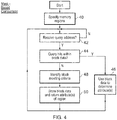
- Figure 4 is a flow diagram schematically illustrating determining one or more memory attributes using a mask based comparison
- Figure 5 is a flow diagram schematically illustrating determining one or more attributes using a page based comparison.
- Figure 1 schematically illustrates a data processing system 2 including a processor core 4, a memory 6 and a memory protection unit 8.
- the memory 6 stores both program instructions to be executed by the processor core 4 and data to be manipulated by the processor core 4.
- the processor core 4 includes a load store unit 10 for performing reads and writes of data values to and from the memory 6.
- An instruction fetch unit 12 fetches program instructions from the memory 6 for supply to an instruction pipeline 14.
- the program instructions are decoded by an instruction decoder 16 which generates control signals for controlling other portions of the processor core 4, such as a general purpose register file, a multiplier 20, a shifter 22 and an adder 4.
- the memory protection unit 8 serves to associate one or more programmable attribute values with memory addresses within the memory address space of the memory 6.
- the memory address space may be divided into a plurality of memory region: the memory addresses within these regions sharing at least one attribute.
- one memory region may be defined as permitting read only memory access operations, while a different memory region may be defined as permitting both read and write memory access operations.
- the memory regions are defined by a base address within the memory address space and a limit address within the memory address space. A memory region extends from its base address to its limit address. The base address and the limit address may be subject to some degree of alignment, such as, for example, 32 byte alignment or 64 byte alignment.
- the base addresses and limit addresses together with the associated attributes for the memory regions they define are stored within a memory regions data store 26 from where they may be accessed by the memory protection unit 8.
- the base addresses, the limit addresses, and the memory attributes may all be programmable so that the system designer can divide the memory address space as they wish and associate different attributes with different memory regions within that memory address space.
- the memory protection unit 8 uses the base address data and the limit address data within the memory regions data store 26 to determine within which of the memory regions, the query address lies. If the memory regions overlap and a query address is identified as falling within more than one memory region, then, in this example embodiment, the query address is treated as invalid. Accordingly, attribute data is returned for a query address when the query address lies within a single memory region.
- the memory protection unit 8 serves to identify a memory block within the memory address space that includes the query address and contiguously extends between a lower block address LBA and an upper block address UBA. These memory blocks may be used to form mask values which together with a TAG value derived from the query address used to generate the respective mask values are stored within a mask-based comparison unit 28. Mask-based comparison may be performed more rapidly than the comparison performed by the memory protection unit 8 against the base address and the limit address.
- the memory protection unit 8 when comparing against the base address and the limit address uses a test that the query address is greater than or equal to the base address and less than or equal to the limit address. Such comparisons are relatively slow.
- the mask-based comparison performed by the mask-based comparison unit 28 may be performed with simple AND operations (or other simple logical operations) as will be described further below.
- a further query address is generated by either the load/store unit 10 or the instruction fetch unit 12, then it is supplied to both the memory protection unit 8 and the mask-based comparison unit 28.
- the mask-based comparison unit 28 is storing mask data and TAG data (together constituting block data) specifying a memory block known to lie wholly within a memory region as previously identified by the memory protection unit 8, then a hit may be registered by the mask-based comparison unit 28 and the attribute data stored therein returned more rapidly and with a lower energy cost compared to the full comparison being performed by the memory protection unit 8.
- the determination performed by the memory protection unit 8 using the base address and the limit address stored within the memory regions data store 26 is such that a single precise region hit for a region within a given N-bit base, limit and enable flag for a given query is computable using:
- this hit value is considered valid if, and only if, one region hits for a given query address. If more than one region hits, then the query address is considered invalid. This permits regions of the memory address space to be marked as invalid and blocked from use by the data processing system 2.
- a memory block is identified for that hit such that corresponding block data (a mask value and a TAG value derived form a query value that generated that mask value) may be stored within the mask-comparison unit 28.
- the processing performed by the memory protection unit 8 to determine a mask value for use with a TAG value that will define a memory block, a lower block address and an upper block address as previously discussed may be as follows for a single region hit with an N-bit base address, a limit address and a query address.
- constant propagation may also be applied in the above calculations based upon the minimum granularity of the memory region definitions, e.g. 32-byte aligned, 64-byte aligned as previously discussed and as a consequence of which a corresponding number of the lowest significant bits of the limit address and the base address may effectively all be zeros.
- the block data When the block data has been formed and stored within the mask-based comparison unit 28, it can be used to identify a hit within that same memory block using a simple bitwise logical AND comparison with the resultant memory block being valid (a hit for which the same memory attributes should be associated) for any subsequent query where:
- the full comparison based upon the greater than or equal to and less than or equal to tests against the base address and the limit address may also be required, for a at least the first access of a query address within a memory block, in order to extract the attributes associated with that memory block and to manage region overlap.
- the memory regions data store 26 serves as region storage for the base address and the limit address together with attribute data associated with the memory regions defined thereby.
- the memory protection unit 8 serves as comparison circuitry for comparing a query address with the base address and the limit address to determine if the query address is within a memory region.
- the memory protection unit 8 also serves as block identifying circuitry to identify a memory block as discussed above.
- the mask-based comparison unit 28 serves as block storage for storing block data defining the memory blocks and as determining circuitry for using the block data to determine if a subsequent query address lies within a memory region.
- Example 1 The results of mask o for all MPU regions can be ANDed together to produce the largest region which does not interact with the boundaries of any region.
- Example 2. Example 3.
- Example 4. query_i 0x1234567 0x1234567 0x1234567 0x0000002 base_i 0x0000000 0x1000000 0x0000001 0x0000001 limit_i 0x7fffff 0x7fffffff 0x7ffffffff delta base 0x091a2b3 0x011a2b3 Ox091a2b3 0x0000001 delta_limit 0x36e5d4c 0x36e5d4c 0x36e5d4c 0x3 ffffe discord base 0x0ffffff 0x01fffff 0x0ffffff 0x0000001 discord_limit 0x3 fffff
- Figure 2 illustrates a further example data processing system 38.
- the example embodiment of Figure 2 includes both a memory protection unit 30 and a memory management unit 32.
- the memory management unit 32 performs page table based memory management using hierarchical page table data 46 stored within the memory 6 and a translation lookaside buffer 30 in a manner that will be familiar to those in this technical field (e.g. page table walks).
- the memory address space is divided into fixed size memory pages, such as, for example, 4kB memory pages. Each of these memory pages has attribute data associated therewith.
- a micro-translation lookaside buffer 34 may be provided to store, for more rapid access, data identifying the most recently used pages of memory together with their attribute data in order to speed up memory access operations and reduce energy consumed.
- the memory protection unit 30, which may be used in some modes of operation instead of the memory management unit 32, divides the memory address space into memory regions defined by base addresses, limit addresses and attributes as previously discussed.
- the micro-translation lookaside buffer 34 is reused by the memory protection unit 30 to store page-based data derived from the memory region data stored within the memory regions data store 26.
- the memory pages which are represented by the entries within the micro-translation lookaside buffer 34 may be considered as replacements for the memory blocks discussed previously in relation to the example embodiment of Figure 1 .
- the memory pages are a fixed size for a given implementation.
- a new page entry may be made within the micro-translation lookaside buffer 34 by the memory protection unit 30 performing the processing described below.
- the base address and the limit address are 64-byte aligned and the bits [4:0] of the addresses may be ignored and the memory pages are 4kB in size as previously mentioned.
- the processing performed by the memory protection unit 30 may be represented as:
- this processing is performed for all of the regions defined by the data stored within the memory region data store 26 and a hit is considered valid if it is the only hit which arises.
- An aligned query address is suitable for inclusion as new page data within the micro-translation lookaside buffer 34 if there is a single true value of "infringes" and the hit region has a true value for "page”.
- Figure 3 schematically illustrates the division of memory address space extending between a bottom of memory and a top of memory into a plurality of memory regions. Each of these memory regions extends between a base address and a limit address. Each of these memory regions has one or more attributes, such as read only, read and write, cacheable, etc associated with it for use with memory addresses within the memory address space falling within that memory region and that do not fall within any of the other memory regions. Memory address space corresponding to overlapping memory regions is considered as invalid and is marked in Figure 3 with "*". When a query address lies within a single memory region, then the attributes associated with that single memory region are returned for the query address concerned by the memory management systems of Figures 1 and 2 .
- Figure 4 is a flow diagram schematically illustrating mask-based comparison in accordance with the example of Figure 1 .
- memory regions are specified and the data defining these memory regions is stored within the memory region data store 26.
- a query address is received.
- Step 44 determines whether or not the received query address hits with the block data stored and used by the mask-based comparison unit 28. If there is a hit, then step 46 serves to use the block data to determine the attributes for the received query address.
- step 48 serves to identify a memory block (if possible) meeting the criteria previously discussed. Such a memory block is identified to have the largest power of two size which is aligned relative to that power of two size and that lies wholly within the memory region for which the hit has occurred.
- Step 50 then stores the block data in the form of the mask value and the TAG (derived from the original query address) as described above into the memory-based comparison unit 28 for further use as well as returning the attribute data which has been read from the memory region.
- FIG. 5 is a flow diagram schematically illustrating the operation of the page-based comparison performed in the example embodiment of Figure 2 .
- memory regions are specified using base addresses and limit addresses together with attribute values and stored within the memory regions data store 26.
- processing waits until a query address is received.
- Step 56 determines whether or not the query address hits within the micro-translation lookaside buffer 34. If there is a hit within the micro-translation lookaside buffer 34, then step 58 uses the page data stored therein to determine the attributes associated with the query address.
- step 60 identifies a page (of the size used by the memory management unit 32 and as defined by the page table data 36), which corresponds to the query address and returns the attributes of the memory region as read from the memory regions data store 26.
- step 62 determines whether the page identified is suitable for storage within the micro-translation lookaside buffer 34 as previously described. If the page table data is suitable for storage and reuse accordingly to the above criteria, then step 64 serves to store the page data into the micro-translation lookaside buffer 34 where it can be used to generate a more rapid hit if another query address arises which lies within that page.
Landscapes
- Engineering & Computer Science (AREA)
- Theoretical Computer Science (AREA)
- Physics & Mathematics (AREA)
- General Engineering & Computer Science (AREA)
- General Physics & Mathematics (AREA)
- Computer Security & Cryptography (AREA)
- Human Computer Interaction (AREA)
- Storage Device Security (AREA)
- Memory System (AREA)
- Memory System Of A Hierarchy Structure (AREA)
Claims (4)
- Verfahren, das Folgendes umfasst:Festlegen (40) einer Basisadresse und einer Grenzadresse in einem Speicheradressraum, um einen Speicherbereich zu definieren, wobei Speicheradressen im Speicherbereich mindestens ein Merkmal gemeinsam verwenden und die Basisadresse und die Grenzadresse einem gewissen Grad einer Ausrichtung, z. B. einer 32 Byte- oder einer 64 Byte-Ausrichtung, unterworfen sind, derart, dass eine Anzahl der niedrigstwertigen Bits der Grenzadresse und der Basisadresse alle Nullen sind,Vergleichen (44) einer Abfrageadresse mit der Basisadresse und der Grenzadresse, um zu bestimmen, ob die Abfrageadresse im Speicherbereich liegt;dann, wenn die Abfrageadresse im Speicherbereich liegt, Identifizieren eines Speicherblocks im Speicheradressraum, der die Abfrageadresse enthält und aneinandergrenzend zwischen einem unteren Adressblock, LBA, und einem oberen Adressblock, UBA, verläuft, wobeiUBA - LBA = 2X, wobei X eine ganze Zahl größer oder gleich null ist;LBA = N × 2X, wobei N eine ganze Zahl größer oder gleich null ist; undWählen von X und N derart, dass der Speicherblock vollständig im Speicherbereich liegt, wobei X derart gewählt wird, dass es einen maximalen ganzzahligen Wert besitzt, für den ein ganzzahliger Wert von N vorliegt, der ermöglicht, dass der Speicherblock vollständig im Speicherbereich liegt;Speichern (50) von Blockdaten, die den Speicherblock repräsentieren, wobei die Blockdaten einen Maskenwert und einen alten Abfragewert, der die Abfrageadresse repräsentiert, die beim Identifizieren des Speicherblocks verwendet wird, umfassen; undVerwenden (46) der Blockdaten, um zu bestimmen, ob eine nachfolgende Abfragedresse im Speicherbereich liegt, wobei das Verwenden der Blockdaten das Bestimmen umfasst, ob ein logischer Vorgang zwischen dem Maskenwert und dem alten Abfragewert mit dem logischen Vorgang zwischen dem Maskenwert und einem neuen Abfragewert, der die nachfolgende Abfrageadresse repräsentiert, übereinstimmt.
- Verfahren nach Anspruch 1, wobei der logische Vorgang ein bitweises UND ist.
- Verfahren nach einem der vorhergehenden Ansprüche, wobei der Speicheradressraum mehrere Speicherbereiche umfasst und ein entsprechender Speicherblock für jeden der mehreren Speicherbereiche, die die Abfrageadresse enthalten, identifiziert wird.
- Vorrichtung, die Folgendes umfasst:einen Bereichsspeicher (26), um eine Basisadresse und eine Grenzadresse in einem Speicheradressraum zu speichern, um einen Speicherbereich zu definieren, wobei Speicheradressen im Speicherbereich mindestens ein Merkmal gemeinsam verwenden und die Basisadresse und die Grenzadresse einem gewissen Grad einer Ausrichtung, z. B. einer 32 Byte- oder einer 64 Byte-Ausrichtung, unterworfen sind, derart, dass eine Anzahl der niedrigstwertigen Bits der Grenzadresse und der Basisadresse alle Nullen sind;eine Vergleichsschaltungsanordnung (8), um eine Abfrageadresse mit der Basisadresse und der Grenzadresse zu vergleichen, um zu bestimmen, ob die Abfrageadresse im Speicherbereich liegt; undeine Blockidentifizierungsschaltung, um dann, wenn die Abfrageadresse im Speicherbereich liegt, einen Speicherblock im Speicheradressraum, der die Abfrageadresse enthält und aneinandergrenzend zwischen einem unteren Adressblock, LBA, und einem oberen Adressblock, UBA, verläuft, zu identifizieren, wobeiUBA - LBA = 2X, wobei X eine ganze Zahl größer oder gleich null ist;LBA = N × 2X, wobei N eine ganze Zahl größer oder gleich null ist; undX und N derart ausgelegt sind, dass der Speicherblock vollständig im Speicherbereich liegt, wobei X derart gewählt wird, dass es einen maximalen ganzzahligen Wert besitzt, für den ein ganzzahliger Wert von N vorliegt, der ermöglicht, dass der Speicherblock vollständig im Speicherbereich liegt;einen Blockspeicher (28), um Blockdaten, die den Speicherblock repräsentieren, zu speichern, wobei die Blockdaten einen Maskenwert und einen alten Abfragewert, der die Abfrageadresse repräsentiert, die beim Identifizieren des Speicherblocks verwendet wird, umfassen; undeine Bestimmungsschaltungsanordnung, um die Blockdaten zu verwenden, um zu bestimmen, ob eine nachfolgende Abfragedresse im Speicherbereich liegt, wobei das Verwenden der Blockdaten das Bestimmen umfasst, ob ein logischer Vorgang zwischen dem Maskenwert und dem alten Abfragewert mit dem logischen Vorgang zwischen dem Maskenwert und einem neuen Abfragewert, der die nachfolgende Abfrageadresse repräsentiert, übereinstimmt.
Priority Applications (3)
| Application Number | Priority Date | Filing Date | Title |
|---|---|---|---|
| EP14195904.9A EP3029574B1 (de) | 2014-12-02 | 2014-12-02 | Speicherverwaltung |
| US14/926,249 US10073620B2 (en) | 2014-12-02 | 2015-10-29 | Memory management |
| JP2015223522A JP7022497B2 (ja) | 2014-12-02 | 2015-11-13 | メモリ管理 |
Applications Claiming Priority (1)
| Application Number | Priority Date | Filing Date | Title |
|---|---|---|---|
| EP14195904.9A EP3029574B1 (de) | 2014-12-02 | 2014-12-02 | Speicherverwaltung |
Publications (2)
| Publication Number | Publication Date |
|---|---|
| EP3029574A1 EP3029574A1 (de) | 2016-06-08 |
| EP3029574B1 true EP3029574B1 (de) | 2019-09-18 |
Family
ID=52002801
Family Applications (1)
| Application Number | Title | Priority Date | Filing Date |
|---|---|---|---|
| EP14195904.9A Active EP3029574B1 (de) | 2014-12-02 | 2014-12-02 | Speicherverwaltung |
Country Status (3)
| Country | Link |
|---|---|
| US (1) | US10073620B2 (de) |
| EP (1) | EP3029574B1 (de) |
| JP (1) | JP7022497B2 (de) |
Families Citing this family (5)
| Publication number | Priority date | Publication date | Assignee | Title |
|---|---|---|---|---|
| US10319457B2 (en) * | 2016-03-21 | 2019-06-11 | International Business Machines Corporation | Methods and systems of testing interfaces of computer storage for storage vulnerabilities |
| JP2017204170A (ja) * | 2016-05-12 | 2017-11-16 | キヤノン株式会社 | 画像処理装置及び画像処理方法 |
| FR3065623B1 (fr) * | 2017-04-28 | 2021-07-09 | Roquette Freres | Albumines de pois ameliorees, procede d'obtention et leurs applications |
| CN109144890B (zh) * | 2018-07-02 | 2021-02-05 | 珠海格力电器股份有限公司 | 一种数据存储方法及装置 |
| US10877788B2 (en) * | 2019-03-12 | 2020-12-29 | Intel Corporation | Processing vectorized guest physical address translation instructions |
Citations (1)
| Publication number | Priority date | Publication date | Assignee | Title |
|---|---|---|---|---|
| US20130290635A1 (en) * | 2010-10-26 | 2013-10-31 | Arm Limited | Provision of access control data within a data processing system |
Family Cites Families (8)
| Publication number | Priority date | Publication date | Assignee | Title |
|---|---|---|---|---|
| US6094713A (en) * | 1997-09-30 | 2000-07-25 | Intel Corporation | Method and apparatus for detecting address range overlaps |
| GB2411027B (en) * | 2002-11-18 | 2006-03-15 | Advanced Risc Mach Ltd | Control of access to a memory by a device |
| US7068545B1 (en) * | 2005-01-04 | 2006-06-27 | Arm Limited | Data processing apparatus having memory protection unit |
| US7805588B2 (en) * | 2005-10-20 | 2010-09-28 | Qualcomm Incorporated | Caching memory attribute indicators with cached memory data field |
| JP2010170266A (ja) * | 2009-01-21 | 2010-08-05 | Toshiba Corp | 半導体集積回路及びアドレス変換方法 |
| US8335908B2 (en) * | 2010-07-01 | 2012-12-18 | Arm Limited | Data processing apparatus for storing address translations |
| WO2014122414A1 (en) * | 2013-02-05 | 2014-08-14 | Arm Limited | Handling memory access operations in a data processing apparatus |
| US9542332B2 (en) * | 2014-11-13 | 2017-01-10 | Via Alliance Semiconductor Co., Ltd. | System and method for performing hardware prefetch tablewalks having lowest tablewalk priority |
-
2014
- 2014-12-02 EP EP14195904.9A patent/EP3029574B1/de active Active
-
2015
- 2015-10-29 US US14/926,249 patent/US10073620B2/en active Active
- 2015-11-13 JP JP2015223522A patent/JP7022497B2/ja active Active
Patent Citations (1)
| Publication number | Priority date | Publication date | Assignee | Title |
|---|---|---|---|---|
| US20130290635A1 (en) * | 2010-10-26 | 2013-10-31 | Arm Limited | Provision of access control data within a data processing system |
Also Published As
| Publication number | Publication date |
|---|---|
| EP3029574A1 (de) | 2016-06-08 |
| JP2016110636A (ja) | 2016-06-20 |
| JP7022497B2 (ja) | 2022-02-21 |
| US20160154586A1 (en) | 2016-06-02 |
| US10073620B2 (en) | 2018-09-11 |
Similar Documents
| Publication | Publication Date | Title |
|---|---|---|
| JP7359837B2 (ja) | メモリ・システム内に記憶されているメモリ保護テーブルを使用するメモリ保護ユニット | |
| KR102357246B1 (ko) | 캐시 교체 정책을 위한 스케일링된 세트 듀얼링 | |
| JP5475055B2 (ja) | キャッシュされたメモリデータを伴うキャッシュメモリ属性インジケータ | |
| CN107735773B (zh) | 用于高速缓冲存储标签压缩的方法及设备 | |
| US10997078B2 (en) | Method, apparatus, and non-transitory readable medium for accessing non-volatile memory | |
| KR102281928B1 (ko) | 가변 변환 색인 버퍼(tlb) 인덱싱 | |
| US10489306B2 (en) | Apparatus and method for processing data, including cache entry replacement performed based upon content data read from candidates selected using victim selection | |
| JP6960933B2 (ja) | 実行許可に基づくキャッシュのライトアロケーション(Write−Allocation) | |
| US10073620B2 (en) | Memory management | |
| JP6478843B2 (ja) | 半導体装置及びキャッシュメモリ制御方法 | |
| IL280089B1 (en) | A binary search procedure for a control table stored in a memory system | |
| KR102355374B1 (ko) | 이종 메모리를 이용하여 메모리 주소 변환 테이블을 관리하는 메모리 관리 유닛 및 이의 메모리 주소 관리 방법 | |
| US9836410B2 (en) | Burst translation look-aside buffer | |
| US10545877B2 (en) | Apparatus and method for accessing an address translation cache | |
| KR20230156062A (ko) | 페이지 재매핑 및 회전들을 통한 어드레스 공간 레이아웃 랜덤화 엔트로피의 증가 | |
| US9934150B1 (en) | Data caching circuit and method | |
| US6950904B2 (en) | Cache way replacement technique | |
| US10621107B1 (en) | Translation lookaside buffer (TLB) clustering system for checking multiple memory address translation entries each mapping a viritual address offset | |
| JP2012003314A (ja) | キャッシュメモリ装置 | |
| CN117349197A (zh) | 内存管理单元和内存访问方法 | |
| GB2628371A (en) | Storing coalesced memory address translations |
Legal Events
| Date | Code | Title | Description |
|---|---|---|---|
| PUAI | Public reference made under article 153(3) epc to a published international application that has entered the european phase |
Free format text: ORIGINAL CODE: 0009012 |
|
| AK | Designated contracting states |
Kind code of ref document: A1 Designated state(s): AL AT BE BG CH CY CZ DE DK EE ES FI FR GB GR HR HU IE IS IT LI LT LU LV MC MK MT NL NO PL PT RO RS SE SI SK SM TR |
|
| AX | Request for extension of the european patent |
Extension state: BA ME |
|
| STAA | Information on the status of an ep patent application or granted ep patent |
Free format text: STATUS: REQUEST FOR EXAMINATION WAS MADE |
|
| 17P | Request for examination filed |
Effective date: 20161207 |
|
| RBV | Designated contracting states (corrected) |
Designated state(s): AL AT BE BG CH CY CZ DE DK EE ES FI FR GB GR HR HU IE IS IT LI LT LU LV MC MK MT NL NO PL PT RO RS SE SI SK SM TR |
|
| STAA | Information on the status of an ep patent application or granted ep patent |
Free format text: STATUS: EXAMINATION IS IN PROGRESS |
|
| 17Q | First examination report despatched |
Effective date: 20180615 |
|
| GRAP | Despatch of communication of intention to grant a patent |
Free format text: ORIGINAL CODE: EPIDOSNIGR1 |
|
| STAA | Information on the status of an ep patent application or granted ep patent |
Free format text: STATUS: GRANT OF PATENT IS INTENDED |
|
| INTG | Intention to grant announced |
Effective date: 20190423 |
|
| GRAS | Grant fee paid |
Free format text: ORIGINAL CODE: EPIDOSNIGR3 |
|
| GRAA | (expected) grant |
Free format text: ORIGINAL CODE: 0009210 |
|
| STAA | Information on the status of an ep patent application or granted ep patent |
Free format text: STATUS: THE PATENT HAS BEEN GRANTED |
|
| AK | Designated contracting states |
Kind code of ref document: B1 Designated state(s): AL AT BE BG CH CY CZ DE DK EE ES FI FR GB GR HR HU IE IS IT LI LT LU LV MC MK MT NL NO PL PT RO RS SE SI SK SM TR |
|
| REG | Reference to a national code |
Ref country code: GB Ref legal event code: FG4D |
|
| REG | Reference to a national code |
Ref country code: CH Ref legal event code: EP |
|
| REG | Reference to a national code |
Ref country code: DE Ref legal event code: R096 Ref document number: 602014053764 Country of ref document: DE |
|
| REG | Reference to a national code |
Ref country code: AT Ref legal event code: REF Ref document number: 1182133 Country of ref document: AT Kind code of ref document: T Effective date: 20191015 |
|
| REG | Reference to a national code |
Ref country code: IE Ref legal event code: FG4D |
|
| REG | Reference to a national code |
Ref country code: NL Ref legal event code: MP Effective date: 20190918 |
|
| PG25 | Lapsed in a contracting state [announced via postgrant information from national office to epo] |
Ref country code: FI Free format text: LAPSE BECAUSE OF FAILURE TO SUBMIT A TRANSLATION OF THE DESCRIPTION OR TO PAY THE FEE WITHIN THE PRESCRIBED TIME-LIMIT Effective date: 20190918 Ref country code: HR Free format text: LAPSE BECAUSE OF FAILURE TO SUBMIT A TRANSLATION OF THE DESCRIPTION OR TO PAY THE FEE WITHIN THE PRESCRIBED TIME-LIMIT Effective date: 20190918 Ref country code: LT Free format text: LAPSE BECAUSE OF FAILURE TO SUBMIT A TRANSLATION OF THE DESCRIPTION OR TO PAY THE FEE WITHIN THE PRESCRIBED TIME-LIMIT Effective date: 20190918 Ref country code: NO Free format text: LAPSE BECAUSE OF FAILURE TO SUBMIT A TRANSLATION OF THE DESCRIPTION OR TO PAY THE FEE WITHIN THE PRESCRIBED TIME-LIMIT Effective date: 20191218 Ref country code: BG Free format text: LAPSE BECAUSE OF FAILURE TO SUBMIT A TRANSLATION OF THE DESCRIPTION OR TO PAY THE FEE WITHIN THE PRESCRIBED TIME-LIMIT Effective date: 20191218 Ref country code: SE Free format text: LAPSE BECAUSE OF FAILURE TO SUBMIT A TRANSLATION OF THE DESCRIPTION OR TO PAY THE FEE WITHIN THE PRESCRIBED TIME-LIMIT Effective date: 20190918 |
|
| REG | Reference to a national code |
Ref country code: LT Ref legal event code: MG4D |
|
| PG25 | Lapsed in a contracting state [announced via postgrant information from national office to epo] |
Ref country code: GR Free format text: LAPSE BECAUSE OF FAILURE TO SUBMIT A TRANSLATION OF THE DESCRIPTION OR TO PAY THE FEE WITHIN THE PRESCRIBED TIME-LIMIT Effective date: 20191219 Ref country code: RS Free format text: LAPSE BECAUSE OF FAILURE TO SUBMIT A TRANSLATION OF THE DESCRIPTION OR TO PAY THE FEE WITHIN THE PRESCRIBED TIME-LIMIT Effective date: 20190918 Ref country code: LV Free format text: LAPSE BECAUSE OF FAILURE TO SUBMIT A TRANSLATION OF THE DESCRIPTION OR TO PAY THE FEE WITHIN THE PRESCRIBED TIME-LIMIT Effective date: 20190918 Ref country code: AL Free format text: LAPSE BECAUSE OF FAILURE TO SUBMIT A TRANSLATION OF THE DESCRIPTION OR TO PAY THE FEE WITHIN THE PRESCRIBED TIME-LIMIT Effective date: 20190918 |
|
| REG | Reference to a national code |
Ref country code: AT Ref legal event code: MK05 Ref document number: 1182133 Country of ref document: AT Kind code of ref document: T Effective date: 20190918 |
|
| PG25 | Lapsed in a contracting state [announced via postgrant information from national office to epo] |
Ref country code: EE Free format text: LAPSE BECAUSE OF FAILURE TO SUBMIT A TRANSLATION OF THE DESCRIPTION OR TO PAY THE FEE WITHIN THE PRESCRIBED TIME-LIMIT Effective date: 20190918 Ref country code: PL Free format text: LAPSE BECAUSE OF FAILURE TO SUBMIT A TRANSLATION OF THE DESCRIPTION OR TO PAY THE FEE WITHIN THE PRESCRIBED TIME-LIMIT Effective date: 20190918 Ref country code: PT Free format text: LAPSE BECAUSE OF FAILURE TO SUBMIT A TRANSLATION OF THE DESCRIPTION OR TO PAY THE FEE WITHIN THE PRESCRIBED TIME-LIMIT Effective date: 20200120 Ref country code: NL Free format text: LAPSE BECAUSE OF FAILURE TO SUBMIT A TRANSLATION OF THE DESCRIPTION OR TO PAY THE FEE WITHIN THE PRESCRIBED TIME-LIMIT Effective date: 20190918 Ref country code: RO Free format text: LAPSE BECAUSE OF FAILURE TO SUBMIT A TRANSLATION OF THE DESCRIPTION OR TO PAY THE FEE WITHIN THE PRESCRIBED TIME-LIMIT Effective date: 20190918 Ref country code: IT Free format text: LAPSE BECAUSE OF FAILURE TO SUBMIT A TRANSLATION OF THE DESCRIPTION OR TO PAY THE FEE WITHIN THE PRESCRIBED TIME-LIMIT Effective date: 20190918 Ref country code: AT Free format text: LAPSE BECAUSE OF FAILURE TO SUBMIT A TRANSLATION OF THE DESCRIPTION OR TO PAY THE FEE WITHIN THE PRESCRIBED TIME-LIMIT Effective date: 20190918 Ref country code: ES Free format text: LAPSE BECAUSE OF FAILURE TO SUBMIT A TRANSLATION OF THE DESCRIPTION OR TO PAY THE FEE WITHIN THE PRESCRIBED TIME-LIMIT Effective date: 20190918 |
|
| PG25 | Lapsed in a contracting state [announced via postgrant information from national office to epo] |
Ref country code: SM Free format text: LAPSE BECAUSE OF FAILURE TO SUBMIT A TRANSLATION OF THE DESCRIPTION OR TO PAY THE FEE WITHIN THE PRESCRIBED TIME-LIMIT Effective date: 20190918 Ref country code: SK Free format text: LAPSE BECAUSE OF FAILURE TO SUBMIT A TRANSLATION OF THE DESCRIPTION OR TO PAY THE FEE WITHIN THE PRESCRIBED TIME-LIMIT Effective date: 20190918 Ref country code: IS Free format text: LAPSE BECAUSE OF FAILURE TO SUBMIT A TRANSLATION OF THE DESCRIPTION OR TO PAY THE FEE WITHIN THE PRESCRIBED TIME-LIMIT Effective date: 20200224 Ref country code: CZ Free format text: LAPSE BECAUSE OF FAILURE TO SUBMIT A TRANSLATION OF THE DESCRIPTION OR TO PAY THE FEE WITHIN THE PRESCRIBED TIME-LIMIT Effective date: 20190918 |
|
| REG | Reference to a national code |
Ref country code: DE Ref legal event code: R097 Ref document number: 602014053764 Country of ref document: DE |
|
| PLBE | No opposition filed within time limit |
Free format text: ORIGINAL CODE: 0009261 |
|
| STAA | Information on the status of an ep patent application or granted ep patent |
Free format text: STATUS: NO OPPOSITION FILED WITHIN TIME LIMIT |
|
| PG2D | Information on lapse in contracting state deleted |
Ref country code: IS |
|
| PG25 | Lapsed in a contracting state [announced via postgrant information from national office to epo] |
Ref country code: DK Free format text: LAPSE BECAUSE OF FAILURE TO SUBMIT A TRANSLATION OF THE DESCRIPTION OR TO PAY THE FEE WITHIN THE PRESCRIBED TIME-LIMIT Effective date: 20190918 Ref country code: IS Free format text: LAPSE BECAUSE OF FAILURE TO SUBMIT A TRANSLATION OF THE DESCRIPTION OR TO PAY THE FEE WITHIN THE PRESCRIBED TIME-LIMIT Effective date: 20200119 |
|
| REG | Reference to a national code |
Ref country code: CH Ref legal event code: PL |
|
| 26N | No opposition filed |
Effective date: 20200619 |
|
| REG | Reference to a national code |
Ref country code: BE Ref legal event code: MM Effective date: 20191231 |
|
| PG25 | Lapsed in a contracting state [announced via postgrant information from national office to epo] |
Ref country code: SI Free format text: LAPSE BECAUSE OF FAILURE TO SUBMIT A TRANSLATION OF THE DESCRIPTION OR TO PAY THE FEE WITHIN THE PRESCRIBED TIME-LIMIT Effective date: 20190918 Ref country code: MC Free format text: LAPSE BECAUSE OF FAILURE TO SUBMIT A TRANSLATION OF THE DESCRIPTION OR TO PAY THE FEE WITHIN THE PRESCRIBED TIME-LIMIT Effective date: 20190918 |
|
| PG25 | Lapsed in a contracting state [announced via postgrant information from national office to epo] |
Ref country code: IE Free format text: LAPSE BECAUSE OF NON-PAYMENT OF DUE FEES Effective date: 20191202 Ref country code: LU Free format text: LAPSE BECAUSE OF NON-PAYMENT OF DUE FEES Effective date: 20191202 |
|
| PG25 | Lapsed in a contracting state [announced via postgrant information from national office to epo] |
Ref country code: LI Free format text: LAPSE BECAUSE OF NON-PAYMENT OF DUE FEES Effective date: 20191231 Ref country code: BE Free format text: LAPSE BECAUSE OF NON-PAYMENT OF DUE FEES Effective date: 20191231 Ref country code: CH Free format text: LAPSE BECAUSE OF NON-PAYMENT OF DUE FEES Effective date: 20191231 |
|
| PG25 | Lapsed in a contracting state [announced via postgrant information from national office to epo] |
Ref country code: CY Free format text: LAPSE BECAUSE OF FAILURE TO SUBMIT A TRANSLATION OF THE DESCRIPTION OR TO PAY THE FEE WITHIN THE PRESCRIBED TIME-LIMIT Effective date: 20190918 |
|
| PG25 | Lapsed in a contracting state [announced via postgrant information from national office to epo] |
Ref country code: MT Free format text: LAPSE BECAUSE OF FAILURE TO SUBMIT A TRANSLATION OF THE DESCRIPTION OR TO PAY THE FEE WITHIN THE PRESCRIBED TIME-LIMIT Effective date: 20190918 Ref country code: HU Free format text: LAPSE BECAUSE OF FAILURE TO SUBMIT A TRANSLATION OF THE DESCRIPTION OR TO PAY THE FEE WITHIN THE PRESCRIBED TIME-LIMIT; INVALID AB INITIO Effective date: 20141202 |
|
| PG25 | Lapsed in a contracting state [announced via postgrant information from national office to epo] |
Ref country code: TR Free format text: LAPSE BECAUSE OF FAILURE TO SUBMIT A TRANSLATION OF THE DESCRIPTION OR TO PAY THE FEE WITHIN THE PRESCRIBED TIME-LIMIT Effective date: 20190918 |
|
| PG25 | Lapsed in a contracting state [announced via postgrant information from national office to epo] |
Ref country code: MK Free format text: LAPSE BECAUSE OF FAILURE TO SUBMIT A TRANSLATION OF THE DESCRIPTION OR TO PAY THE FEE WITHIN THE PRESCRIBED TIME-LIMIT Effective date: 20190918 |
|
| P01 | Opt-out of the competence of the unified patent court (upc) registered |
Effective date: 20230429 |
|
| PGFP | Annual fee paid to national office [announced via postgrant information from national office to epo] |
Ref country code: DE Payment date: 20251126 Year of fee payment: 12 |
|
| PGFP | Annual fee paid to national office [announced via postgrant information from national office to epo] |
Ref country code: GB Payment date: 20251119 Year of fee payment: 12 |
|
| PGFP | Annual fee paid to national office [announced via postgrant information from national office to epo] |
Ref country code: FR Payment date: 20251120 Year of fee payment: 12 |