EP3029034B1 - Benzotriazole derivatives and organic electroluminescent element - Google Patents
Benzotriazole derivatives and organic electroluminescent element Download PDFInfo
- Publication number
- EP3029034B1 EP3029034B1 EP14832687.9A EP14832687A EP3029034B1 EP 3029034 B1 EP3029034 B1 EP 3029034B1 EP 14832687 A EP14832687 A EP 14832687A EP 3029034 B1 EP3029034 B1 EP 3029034B1
- Authority
- EP
- European Patent Office
- Prior art keywords
- layer
- organic
- compound
- electron
- hole
- Prior art date
- Legal status (The legal status is an assumption and is not a legal conclusion. Google has not performed a legal analysis and makes no representation as to the accuracy of the status listed.)
- Active
Links
- YICKQLUSTZRQPW-UHFFFAOYSA-N c1cc2cccc(-c3cc4n[n](-c(cc5)ccc5-c5c(cccc6)c6c(-c6cccnc6)c6c5cccc6)nc4c(-c4cccc5c4cccc5)c3)c2cc1 Chemical compound c1cc2cccc(-c3cc4n[n](-c(cc5)ccc5-c5c(cccc6)c6c(-c6cccnc6)c6c5cccc6)nc4c(-c4cccc5c4cccc5)c3)c2cc1 YICKQLUSTZRQPW-UHFFFAOYSA-N 0.000 description 1
Images


Classifications
-
- C—CHEMISTRY; METALLURGY
- C07—ORGANIC CHEMISTRY
- C07D—HETEROCYCLIC COMPOUNDS
- C07D401/00—Heterocyclic compounds containing two or more hetero rings, having nitrogen atoms as the only ring hetero atoms, at least one ring being a six-membered ring with only one nitrogen atom
- C07D401/02—Heterocyclic compounds containing two or more hetero rings, having nitrogen atoms as the only ring hetero atoms, at least one ring being a six-membered ring with only one nitrogen atom containing two hetero rings
- C07D401/10—Heterocyclic compounds containing two or more hetero rings, having nitrogen atoms as the only ring hetero atoms, at least one ring being a six-membered ring with only one nitrogen atom containing two hetero rings linked by a carbon chain containing aromatic rings
-
- C—CHEMISTRY; METALLURGY
- C07—ORGANIC CHEMISTRY
- C07D—HETEROCYCLIC COMPOUNDS
- C07D401/00—Heterocyclic compounds containing two or more hetero rings, having nitrogen atoms as the only ring hetero atoms, at least one ring being a six-membered ring with only one nitrogen atom
- C07D401/14—Heterocyclic compounds containing two or more hetero rings, having nitrogen atoms as the only ring hetero atoms, at least one ring being a six-membered ring with only one nitrogen atom containing three or more hetero rings
-
- H—ELECTRICITY
- H10—SEMICONDUCTOR DEVICES; ELECTRIC SOLID-STATE DEVICES NOT OTHERWISE PROVIDED FOR
- H10K—ORGANIC ELECTRIC SOLID-STATE DEVICES
- H10K85/00—Organic materials used in the body or electrodes of devices covered by this subclass
- H10K85/60—Organic compounds having low molecular weight
- H10K85/615—Polycyclic condensed aromatic hydrocarbons, e.g. anthracene
-
- H—ELECTRICITY
- H10—SEMICONDUCTOR DEVICES; ELECTRIC SOLID-STATE DEVICES NOT OTHERWISE PROVIDED FOR
- H10K—ORGANIC ELECTRIC SOLID-STATE DEVICES
- H10K85/00—Organic materials used in the body or electrodes of devices covered by this subclass
- H10K85/60—Organic compounds having low molecular weight
- H10K85/615—Polycyclic condensed aromatic hydrocarbons, e.g. anthracene
- H10K85/626—Polycyclic condensed aromatic hydrocarbons, e.g. anthracene containing more than one polycyclic condensed aromatic rings, e.g. bis-anthracene
-
- H—ELECTRICITY
- H10—SEMICONDUCTOR DEVICES; ELECTRIC SOLID-STATE DEVICES NOT OTHERWISE PROVIDED FOR
- H10K—ORGANIC ELECTRIC SOLID-STATE DEVICES
- H10K85/00—Organic materials used in the body or electrodes of devices covered by this subclass
- H10K85/60—Organic compounds having low molecular weight
- H10K85/649—Aromatic compounds comprising a hetero atom
- H10K85/654—Aromatic compounds comprising a hetero atom comprising only nitrogen as heteroatom
-
- H—ELECTRICITY
- H10—SEMICONDUCTOR DEVICES; ELECTRIC SOLID-STATE DEVICES NOT OTHERWISE PROVIDED FOR
- H10K—ORGANIC ELECTRIC SOLID-STATE DEVICES
- H10K85/00—Organic materials used in the body or electrodes of devices covered by this subclass
- H10K85/60—Organic compounds having low molecular weight
- H10K85/649—Aromatic compounds comprising a hetero atom
- H10K85/657—Polycyclic condensed heteroaromatic hydrocarbons
- H10K85/6572—Polycyclic condensed heteroaromatic hydrocarbons comprising only nitrogen in the heteroaromatic polycondensed ring system, e.g. phenanthroline or carbazole
-
- H—ELECTRICITY
- H10—SEMICONDUCTOR DEVICES; ELECTRIC SOLID-STATE DEVICES NOT OTHERWISE PROVIDED FOR
- H10K—ORGANIC ELECTRIC SOLID-STATE DEVICES
- H10K50/00—Organic light-emitting devices
- H10K50/10—OLEDs or polymer light-emitting diodes [PLED]
- H10K50/11—OLEDs or polymer light-emitting diodes [PLED] characterised by the electroluminescent [EL] layers
-
- H—ELECTRICITY
- H10—SEMICONDUCTOR DEVICES; ELECTRIC SOLID-STATE DEVICES NOT OTHERWISE PROVIDED FOR
- H10K—ORGANIC ELECTRIC SOLID-STATE DEVICES
- H10K50/00—Organic light-emitting devices
- H10K50/10—OLEDs or polymer light-emitting diodes [PLED]
- H10K50/14—Carrier transporting layers
- H10K50/16—Electron transporting layers
-
- H—ELECTRICITY
- H10—SEMICONDUCTOR DEVICES; ELECTRIC SOLID-STATE DEVICES NOT OTHERWISE PROVIDED FOR
- H10K—ORGANIC ELECTRIC SOLID-STATE DEVICES
- H10K50/00—Organic light-emitting devices
- H10K50/10—OLEDs or polymer light-emitting diodes [PLED]
- H10K50/18—Carrier blocking layers
Definitions
- This invention relates to novel benzotriazole derivatives and to organic electroluminescent devices that have an organic layer containing the above derivatives between the electrodes.
- An organic electroluminescent device (hereinafter often called an organic EL device) is a spontaneously luminous device which features higher brightness and higher legibility than those of the liquid crystal devices enabling vivid display to be attained and has, therefore, been vigorously studied.
- the above organic EL device is constituted by laminating layers of a fluorescent body capable of transporting electrons and an organic material capable of transporting holes. Upon injecting both electric charges into the layer of the fluorescent body to emit light, the device is capable of attaining a brightness of as high as 1000 cd/m 2 or more with a voltage of not higher than 10 V.
- the organic EL device has been widely known having a structure comprising an anode, a hole injection layer, a hole-transporting layer, a luminous layer, an electron-transporting layer, an electron injection layer and a cathode which are arranged in this order on a substrate more finely dividing the roles required for the organic layers between the electrodes than ever before.
- the device of this kind is achieving a high efficiency and a high durability.
- the electric charges injected from the two electrodes recombine together in the luminous layer to emit light.
- what is important is that how efficiently both electric charges of holes and electrons be handed over to the luminous layer.
- the holes and electrons recombine together at an increased probability.
- the electron-transporting material plays an important role, and it has been urged to provide an electron-transporting material that has a large electron -injection property, a large electron mobility, a high hole-blocking capability and a large durability against the holes.
- the heat resistance and amorphousness of the material also serve as important factors .
- the material having small heat resistance is subject to be thermally decomposed even at low temperatures due to the heat generated when the device is driven, and is deteriorated.
- the material having low amorphousness permits the thin film thereof to be crystallized in short periods of time and, therefore, the device to be deteriorated. Therefore, the material to be used must have large heat resistance and good amorphousness.
- Tris(8-hydroxyquinoline) aluminum (hereinafter abbreviated as Alq 3 ) which is a representative luminous material has also been generally used as an electron-transporting material having, however, a low electron mobility and a work function of 5.6 eV and, therefore, having a hole-blocking capability which is far from satisfactory.
- a method of inserting a hole-blocking layer is one of the measures for preventing the holes from partly passing through the luminous layer to improve the probability of recombination of the electric charge in the luminous layer.
- a hole-blocking material used for forming the hole-blocking layer for example, there have been known triazole derivatives (see, for example, a patent document 1), bathocuproin (hereinafter abbreviated as BCP) and a mixed ligand complex of aluminum [aluminum(III)bis(2-methyl-8-quinolinato)-4-phenyl phenolate (hereinafter abbreviated as BAlq).
- BCP bathocuproin
- BAlq mixed ligand complex of aluminum [aluminum(III)bis(2-methyl-8-quinolinato)-4-phenyl phenolate
- TAZ 3-(4-biphenylyl)-4-phenyl-5-(4-t-butylphenyl)-1,2,4-triazol e
- the TAZ has a work function of as large as 6.6 eV and a large hole-blocking power, and is used for forming an electron-transporting hole-blocking layer that is laminated on the cathode side of a fluorescent luminous layer or a phosphorescent luminous layer prepared by vacuum evaporation or by coating and, therefore, contributes to improving the efficiency of the organic EL devices.
- the TAZ had to be used in combination with an electron-transporting material having a higher electron-transporting capability.
- the BCP too, has a work function of as large as 6.7 eV and a large hole-blocking power but a glass transition point (Tg) of as low as 83°C.
- Tg glass transition point
- the BCP lacks stability and cannot be said to work as a hole-blocking layer to a sufficient degree
- Patent Documents 3-5 and Non Patent Document 1 disclose benzodiazole- and benzotriazole- derivatives, and their use in organic light emitting devices.
- the above-mentioned materials all lack stability if they are used in the form of a film or are not capable of blocking the holes to a sufficient degree.
- Patent Documents
- Non Patent Document 1 " Bipyridyl-substituted benzo[1,2,3]triazoles as a thermally stable electron transporting material for organic light-emitting devices", J. Mater. Chem., 2011, 21, 11791 .
- the object of the present invention is to provide an organic compound that excels in electron injection/transporting capability, features a high hole-blocking power and a high stability in the form of a thin film, and can be used as a material for producing highly efficient and highly durable organic electroluminescent devices, and to provide highly efficient and highly durable organic electroluminescent devices formed by using the above compound.
- the present invention relates to the benzotriazole derivatives of claim 1.
- an organic electroluminescent device having a pair of electrodes and at least one organic layer held therebetween, wherein at least the one organic layer contains the benzotriazole derivatives according to claim 1.
- the organic layer containing the benzotriazole derivatives of claim 1 may be any one of an electron-transporting layer, a hole-blocking layer, a luminous layer or an electron injection layer.
- the benzotriazole derivatives of claim 1 are novel compounds having a benzotriazole ring, and feature the following properties.
- the benzotriazole derivatives of the invention remain stable in the form of a thin film, can be used as an organic layer that is provided between the electrodes of the organic EL device, and are capable of imparting the following properties to the organic EL device:
- the benzotriazole derivatives of the invention feature high electron injection drift speed. If the benzotriazole derivatives are used as a material for constituting the electron injection layer and/or the electron-transporting layer of the organic EL device, therefore, the efficiency is improved for transporting the electrons from the electron-transporting layer into the luminous layer, the luminous efficiency is improved, the driving voltage is lowered, and the durability of the organic EL device can be improved.
- the benzotriazole derivatives of the invention are used as a material for constituting the hole-blocking layer of the organic EL device, it is made possible to realize a high luminous efficiency owing to their excellent hole-blocking power, electron-transporting property and stability in the form of a thin film and, at the same time, to lower the driving voltage, to improve durability against the electric current and, therefore, to attain improved maximum brightness of the organic EL device.
- the benzotriazole derivatives are used as a host material to carry a fluorescent material or a luminous phosphor called dopant thereon so as to form a luminous layer. This makes it possible to realize the organic EL device that drives on a decreased voltage and features an improved the luminous efficiency.
- the benzotriazole derivatives of the invention as a material for constituting organic layers of the organic EL device to utilize their characteristics, it is made possible to confine the excitons formed in the luminous layer, to improve the probability of recombining the holes with the electrons, to attain a high luminous efficiency, to lower the driving voltage and to realize a high efficiency and a high degree of durability.
- the benzotriazole derivatives of the present invention are represented by the structures in claim 1.
- benzotriazole derivatives of the present invention have high melting points and high glass transition points (Tg), are capable of forming thin films having excellent heat resistance and are capable of maintaining amorphous state with stability. Besides, these compounds permit electrons to drift faster than the conventional electron-transporting materials, have excellent hole-blocking power, remain stable in the state of thin films and, therefore, can be used for fabricating an organic EL device that features elongated service life.
- the hole-blocking power of the benzotriazole derivatives of the invention can be evaluated in terms of work functions. As also demonstrated in Examples appearing later, the work functions are measured by forming a thin film of 100 nm on an ITO substrate and by using an ionization potential-measuring apparatus (model PYS-202 manufactured by Sumitomo Heavy Industries, Ltd.).
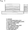
- the organic EL device having the organic layer formed by using the above benzotriazole derivative of the present invention has a structure as shown, for example, in Fig. 7 .
- a transparent anode 2 a hole injection layer 3, a hole-transporting layer 4, a luminous layer 5, a hole-blocking layer 6, an electron-transporting layer 7, an electron injection layer 8 and a cathode 9 are formed on a glass substrate 1 (which may be any transparent substrate such as transparent resin substrate or the like substrate).
- the organic EL device to which the benzotriazole derivative of the present invention is applied is not limited to the one of the above layer structure, as a matter of course, and an electron-blocking layer and the like can be formed between the hole-transporting layer 4 and the luminous layer 5.
- the organic EL device may have a simplified layer structure omitting the electron injection layer 8 or the hole injection layer 3. For instance, some layers can be omitted from the above multilayer structure.
- the organic EL device can be fabricated in a simple layer structure having the anode 2, hole-transporting layer 4, luminous layer 5, electron-transporting layer 7 and cathode 9 formed on the substrate 1.
- the benzotriazole derivative of the invention is preferably used as a material for forming organic layers (e.g. , luminous layer 5, hole-blocking layer 6, electron-transporting layer 7 and electron injection layer 8) between the anode 2 and the cathode 9.
- organic layers e.g. , luminous layer 5, hole-blocking layer 6, electron-transporting layer 7 and electron injection layer 8
- the transparent anode 2 may be formed by using an electrode material which has been known per se, i.e., by vapor-depositing an electrode material having a large work function, such as ITO or gold on the substrate 1 (transparent substrate such as glass substrate or the like).
- the hole injection layer 3 can be formed on the transparent anode 2 by using the materials that have been known per se, such as those described below.
- PEDOT poly(3,4-ethylenedioxythiophene)
- PSS poly(styrene sulfonate)
- the layer (thin film) can be formed by using the above materials relying not only upon the vacuum evaporation method but also upon the known methods such as spin-coating method or ink-jet method.
- the layers described below, too, can similarly be formed by the vacuum evaporation, the spin-coating or the ink-jet method.
- the hole-transporting layer 4, too, can be formed on the hole injection layer 3 by using a hole-transporting material that has been known per se.
- Representative examples of the hole-transporting materials are:
- the compounds for forming the hole-transporting layer may be used alone to form a film or may be used being mixed together in two or more kinds to form a film. Or the above compounds may be used in one kind or in a plurality of kinds to form a plurality of layers, and a multiplicity of films formed by laminating such layers may be used as a hole-transporting layer.
- the hole injection transporting layer can be formed by being coated with a high molecular material such as poly(3,4-ethylenedioxythiophene) (hereinafter abbreviated as PEDOT) or polystyrene sulfonate (hereinafter abbreviated as PSS) .
- PEDOT poly(3,4-ethylenedioxythiophene)
- PSS polystyrene sulfonate
- the material usually used for forming the layer may, further, be P-doped with a trisbromophenylaminehexachloroantimony or the like. It is also allowable to form the hole-transporting layer 4 (or the hole injection layer 3) by using a high molecular compound having a basic skeleton of TPD.
- the electron-blocking layer (that canbe formed between the hole-transporting layer 4 and the luminous layer 5) that has not been shown, there can be used a known electron-blocking compound having the electron-blocking action, such as carbazole derivative or a compound that has a triphenylsilyl group and a triarylamine structure. Described below are concrete examples of the carbazole derivative and the compound having the triarylamine structure.
- TCTA 4,4',4"-Tri(N-carbazolyl)triphenylamine
- mCP 1,3-Bis(carbazole-9-il)benzene
- Ad-Cz 2,2-Bis(4-carbazole-9-ilphenyl)adamantane
- the electron-blocking layer is formed by using one, two or more kinds of the above known electron-blocking materials. It is also allowable to form a plurality of layers by using one or a plurality of kinds of the electron-blocking materials, and use a multiplicity of films formed by laminating such layers as the electron-blocking layer.
- the luminous layer 5 of the organic EL device can be formed by using the benzotriazole derivative of the invention as the luminous material.
- the luminous layer 5 can also be formed by using luminous materials such as a metal complex of a quinolynol derivative as represented by Alq 3 , various metal complexes such as of zinc, beryllium and aluminum, anthracene derivatives, bisstyrylbenzene derivatives, pyrene derivatives, oxazole derivatives and polyparaphenylenevinylene derivatives.
- thiazole derivative As the host material in this case, there canbe used thiazole derivative, benzimidazole derivative and polydialkylfluorene derivative in addition to the above luminous materials.
- the dopant material there can be used quinacridone, cumalin, rubrene, perylene and derivatives thereof, benzopyran derivatiive, rhodamine derivative and aminostyryl derivative.
- the luminous layer 5, too, can be formed in a single-layer structure by using one or two or more kinds of the luminous materials, or in a multi-layer structure by laminating a plurality of layers.
- the phosphorescent luminous material there can be used a phosphorescent luminous body of a metal complex such as of iridium or platinum.
- a green luminous phosphor such as Ir(ppy) 3
- a blue luminous phosphor such as Flrpic or Flr 6
- a red luminous phosphor such as Btp 2 lr(acac).
- These phosphorescent luminous materials are used by being doped in the hole injection transporting host material or in the electron-transporting host material.
- carbazole derivatives such as 4,4'-di(N-carbazolyl)biphenyl (hereinafter abbreviated as CBP), TCTA or mCP in addition to using the benzotriazole derivative of the present invention.
- the electron-transporting host material there can be used p-bis (triphenylsilyl) benzene (hereinafter abbreviated as UGH2) or 2,2',2"-(1,3,5-phenylene)-tris (1-phenyl-1H-benzimidazole) (hereinafter abbreviated as TPBI) .
- UGH2 triphenylsilyl
- TPBI 2,2',2"-(1,3,5-phenylene)-tris (1-phenyl-1H-benzimidazole)
- the host material is desirably doped with the phosphorescent luminous material in an amount in a range of 1 to 30% by weight relative to the whole luminous layer relying on the vacuum coevaporation.
- the luminous material further, it is also allowable to use a material that emits retarded fluorescence, such as CDCB derivative like PIC-TRZ, CC2TA, PXZ-TRZ or 4CzlPN (see Appl. Phys. Let., 98, 083302 (2011 )).
- a material that emits retarded fluorescence such as CDCB derivative like PIC-TRZ, CC2TA, PXZ-TRZ or 4CzlPN (see Appl. Phys. Let., 98, 083302 (2011 )).
- the hole-blocking layer 6 can also be formed between the luminous layer 5 and the electron-transporting layer 7 by using a known compound having the hole-blocking action in addition to using the benzotriazole derivative of the present invention.
- Phenanthroline derivatives such as bathocuproin (hereinafter abbreviated as BCP) and the like; Metal complexes of quinolinol derivatives such as aluminum(III)bis(2-methyl-8-quinolinato)-4-phenylphenolate (hereinafter abbreviated as BAlq) and the like; Various rare earth complexes; Triazole derivatives; Triazine derivatives; and Oxadiazole derivatives.
- the hole-blocking layer 6 and the electron-transporting layer 7 can be formed as one layer.
- the hole-blocking layer 6, too, can be formed in the structure of a single layer or of a laminate of a multiplicity of layers, the layers being formed by using one kind or two or more kinds of the above-mentioned compounds having hole-blocking action.
- the electron-transporting layer 7 can be formed by using electron-transporting compounds that have been known per se. such as metal complexes of quinolinol derivatives like Alq 3 and BAlq, various metal complexes, triazole derivatives, triazine derivatives, oxadiazole derivatives, thiadiazole derivatives, carbodiimide derivatives, quinoxaline derivatives, phenanthroline derivatives and silole derivatives in addition to using the benzotriazole derivatives of the present invention.
- electron-transporting compounds that have been known per se. such as metal complexes of quinolinol derivatives like Alq 3 and BAlq, various metal complexes, triazole derivatives, triazine derivatives, oxadiazole derivatives, thiadiazole derivatives, carbodiimide derivatives, quinoxaline derivatives, phenanthroline derivatives and silole derivatives in addition to using the benzotriazole derivatives of the present invention.
- the electron-transporting layer 7, too, can be formed in the structure of a single layer or of a laminate of a multiplicity of layers, the layers being formed by using one kind or two or more kinds of the above-mentioned electron-transporting compounds.
- the electron injection layer 8, too, can be formed by using known compounds, i.e., by using alkali metal salts such as lithium fluoride and cesium fluoride, alkaline earth metal salts such as magnesium fluoride, and metal oxides such as aluminum oxide in addition to using the benzotriazole derivatives of the present invention.
- alkali metal salts such as lithium fluoride and cesium fluoride
- alkaline earth metal salts such as magnesium fluoride
- metal oxides such as aluminum oxide in addition to using the benzotriazole derivatives of the present invention.
- the electron injection layer 8 or the electron-transporting layer 7 may be formed by using materials that have usually been used for forming these layers but that are N-doped with a metal such as cesium or the like.
- an electrode material having a low work function such as aluminum
- an electrode material of an alloy having a lower work function such as magnesium-silver alloy, magnesium-indium alloy or aluminum-magnesium alloy.
- the organic EL device forming at least one of the organic layers (e.g., electron injection layer 8, electron-transporting layer 7, hole-blocking layer 6 or luminous layer 5) by using the benzotriazole derivative of the present invention, features a high luminous efficiency, a high power efficiency, a low practical driving voltage, a low luminance start voltage and very excellent durability.
- the organic layers e.g., electron injection layer 8, electron-transporting layer 7, hole-blocking layer 6 or luminous layer 5
- the organic EL device forming at least one of the organic layers (e.g., electron injection layer 8, electron-transporting layer 7, hole-blocking layer 6 or luminous layer 5) by using the benzotriazole derivative of the present invention, features a high luminous efficiency, a high power efficiency, a low practical driving voltage, a low luminance start voltage and very excellent durability.
- Fig. 1 shows the results of the 1 H-NMR measurement.
- Fig. 2 shows the results of the 1 H-NMR measurement.
- Fig. 3 shows the results of the 1 H-NMR measurement.
- Fig. 4 shows the results of the 1 H-NMR measurement.
- Fig. 5 shows the results of the 1 H-NMR measurement.
- Fig. 6 shows the results of the 1 H-NMR measurement.
- the compounds of the present invention have glass transition points which are not lower than 100°C and, specifically, not lower than 150°C, or which are not observed indicating that the thin films formed by using the compounds of the invention remain stable.
- the compounds have high melting points and large heat resistances.
- the compounds of Examples 1 to 5 have differences between the melting points and the glass transition points of not less than 30°C and are easy to handle.
- films were vapor-deposited in a thickness of 100 nm on an ITO substrate and were measured for their work functions by using an apparatus for measuring ionization potentials (Model PYS-202 manufactured by Sumitomo Heavy Industries, Ltd.). The results were as follows: Work functions Compound of Ex. 1 5.91 eV Compound of Ex. 2 5.94 eV Compound of Ex. 3 5.85 eV Compound of Ex. 4 5.91 eV Compound of Ex. 5 6.22 eV Compound of Ex. 6 6.21 eV
- the compounds of the present invention have values larger than a work function of 5.5 eV possessed by general hole-transporting materials such as NPD, TPD and the like, and have large hole-blocking powers.
- An organic EL device of a structure shown in Fig. 7 was fabricated in a manner as described below by using the compound obtained in Example 1.
- a glass substrate 1 on which the ITO film has been formed in a thickness of 150 nm was washed with an organic solvent and was, thereafter, washed for its surfaces by an oxygen plasma treatment.
- the glass substrate with the ITO electrode was placed in a vacuum evaporation machine, and the pressure therein was reduced down to 0.001 Pa or lower.
- a compound HIM-1 of the following structural formula was vapor-deposited at a deposition rate of 6 nm/min. in a thickness of 20 nm so as to cover the transparent anode 2.
- a compound HTM-1 of the following structural formula was vapor-deposited as the hole-transporting layer 4 at a deposition rate of 6 nm/min. in a thickness of 40 nm.
- the compound 12 synthesized in Example 1 was vapor-deposited at a deposition rate of 6 nm/min. in a thickness of 30 nm so as to work as both the hole-blocking layer 6 and the electron-transporting layer 7.
- the electron injection layer 8 was formed in a thickness of 0.5 nm by vapor-depositing lithium fluoride at a deposition rate of 0.6 nm/min.
- the thus fabricated organic EL device was impressed with a DC voltage to measure the luminous properties which were as collectively shown in Table 1.
- An organic EL device was fabricated in the same manner as in Example 9 but using the compound (compound 13) of Example 2 instead of using the compound (compound 12) of Example 1 to form the hole-blocking layer/electron-transporting layer in a thickness of 30 nm.
- the organic EL device was measured for its properties in the atmosphere at normal temperature.
- the organic EL device was impressed with a DC voltage to measure the luminous properties which were as collectively shown in Table 1.
- An organic EL device was fabricated in the same manner as in Example 9 but using the compound (compound 14) of Example 3 instead of using the compound (compound 12) of Example 1 to form the hole-blocking layer/electron-transporting layer in a thickness of 30 nm. The thus fabricated organic EL device was measured for its properties in the atmosphere at normal temperature.
- the thus fabricated organic EL device was impressed with a DC voltage to measure the luminous properties which were as collectively shown in Table 1.
- An organic EL device was fabricated in the same manner as in Example 9 but using the compound (compound 15) of Example 4 instead of using the compound (compound 12) of Example 1 to form the hole-blocking layer/electron-transporting layer in a thickness of 30 nm. The thus fabricated organic EL device was measured for its properties in the atmosphere at normal temperature.
- the thus fabricated organic EL device was impressed with a DC voltage to measure the luminous properties which were as collectively shown in Table 1.
- An organic EL device was fabricated in the same manner as in Example 9 but using the compound (compound 62) of Example 6 instead of using the compound (compound 12) of Example 1 to form the hole-blocking layer/electron-transporting layer in a thickness of 30 nm. The thus fabricated organic EL device was measured for its properties in the atmosphere at normal temperature.
- the thus fabricated organic EL device was impressed with a DC voltage to measure the luminous properties which were as collectively shown in Table 1.
- An organic EL device was fabricated in the same manner as in Example 9 but using the compound (ETM-1) of the following structural formula instead of using the compound (compound 12) of Example 1 to form the hole-blocking layer / electron-transporting layer in a thickness of 30 nm.
- the thus fabricated organic EL device was measured for its properties in the atmosphere at normal temperature.
- the thus fabricated organic EL device was impressed with a DC voltage to measure the luminous properties which were as collectively shown in Table 1.
- the organic EL devices of Examples to 13 of the invention have driving voltages of as low as 4.95 to 5.10 V as compared to 5.95 V of the organic EL device of Comparative Example 1 that uses the ETM-1 of the above structural formula. Further, the organic EL devices of Examples 9 to 13 of the invention exhibit current efficiencies of 8.32 to 8.45 cd/A which are great improvements over 7.92 cd/A of the organic EL device of Comparative Example 1.
- the organic EL devices of Examples 11 to 13 of the invention exhibit power efficiencies of 5.19 to 5.28 lm/W which are great improvements over 4.19 lm/W of the organic EL device of Comparative Example 1.
- the organic EL devices of the present invention are capable of achieving a great decrease in the practical driving voltages and great improvement in the luminous efficiency and power efficiency as compared to the devices that use the ETM-1 of the above structural formula that has been generally used as an electron-transporting material.
- the benzotriazole derivatives of the present invention have good electron injection property and excellent hole-blocking power, remain stable in their thin film state, and can be used as excellent compounds for fabricating the organic EL devices.
- Upon fabricating the organic EL devices by using the above compounds further, it is allowed to attain a high luminous efficiency and power efficiency while lowering the practical driving voltage and improving the durability. Their use can, therefore, be expanded to, for example, domestic appliances and illumination equipment.
Landscapes
- Chemical & Material Sciences (AREA)
- Organic Chemistry (AREA)
- Physics & Mathematics (AREA)
- Spectroscopy & Molecular Physics (AREA)
- Engineering & Computer Science (AREA)
- Materials Engineering (AREA)
- Electroluminescent Light Sources (AREA)
- Plural Heterocyclic Compounds (AREA)
Description
- This invention relates to novel benzotriazole derivatives and to organic electroluminescent devices that have an organic layer containing the above derivatives between the electrodes.
- An organic electroluminescent device (hereinafter often called an organic EL device) is a spontaneously luminous device which features higher brightness and higher legibility than those of the liquid crystal devices enabling vivid display to be attained and has, therefore, been vigorously studied.
- In 1987, C. W. Tang et al. of Eastman Kodak Company have developed a device of a layer-laminated structure comprising various kinds of materials to bear individual roles, and have put an organic EL device using organic materials into a practical use. The above organic EL device is constituted by laminating layers of a fluorescent body capable of transporting electrons and an organic material capable of transporting holes. Upon injecting both electric charges into the layer of the fluorescent body to emit light, the device is capable of attaining a brightness of as high as 1000 cd/m2 or more with a voltage of not higher than 10 V.
- So far, very many improvements have been made to put the organic EL device to practical use. For example, the organic EL device has been widely known having a structure comprising an anode, a hole injection layer, a hole-transporting layer, a luminous layer, an electron-transporting layer, an electron injection layer and a cathode which are arranged in this order on a substrate more finely dividing the roles required for the organic layers between the electrodes than ever before. The device of this kind is achieving a high efficiency and a high durability.
- To further improve the luminous efficiency, attempts have been made toutilize triplet excitons and study has been forwarded to utilize a phosphorescent luminous compound.
- In the organic EL device, the electric charges injected from the two electrodes recombine together in the luminous layer to emit light. Here, however, what is important is that how efficiently both electric charges of holes and electrons be handed over to the luminous layer. Upon increasing the injection of electrons and their mobility, the holes and electrons recombine together at an increased probability. Further, upon confining the excitons formed in the luminous layer, a high luminous efficiency can be attained. Therefore, the electron-transporting material plays an important role, and it has been urged to provide an electron-transporting material that has a large electron -injection property, a large electron mobility, a high hole-blocking capability and a large durability against the holes.
- As for the life of the device, further, the heat resistance and amorphousness of the material also serve as important factors . The material having small heat resistance is subject to be thermally decomposed even at low temperatures due to the heat generated when the device is driven, and is deteriorated. The material having low amorphousness permits the thin film thereof to be crystallized in short periods of time and, therefore, the device to be deteriorated. Therefore, the material to be used must have large heat resistance and good amorphousness.
- Tris(8-hydroxyquinoline) aluminum (hereinafter abbreviated as Alq3) which is a representative luminous material has also been generally used as an electron-transporting material having, however, a low electron mobility and a work function of 5.6 eV and, therefore, having a hole-blocking capability which is far from satisfactory.
- A method of inserting a hole-blocking layer is one of the measures for preventing the holes from partly passing through the luminous layer to improve the probability of recombination of the electric charge in the luminous layer.
- As a hole-blocking material used for forming the hole-blocking layer, for example, there have been known triazole derivatives (see, for example, a patent document 1), bathocuproin (hereinafter abbreviated as BCP) and a mixed ligand complex of aluminum [aluminum(III)bis(2-methyl-8-quinolinato)-4-phenyl phenolate (hereinafter abbreviated as BAlq).
- As an electron-transporting material having excellent hole-blocking property, further, there has been proposed a 3-(4-biphenylyl)-4-phenyl-5-(4-t-butylphenyl)-1,2,4-triazol e (hereinafter abbreviated as TAZ) (see, for example, a patent document 2).
- The TAZ has a work function of as large as 6.6 eV and a large hole-blocking power, and is used for forming an electron-transporting hole-blocking layer that is laminated on the cathode side of a fluorescent luminous layer or a phosphorescent luminous layer prepared by vacuum evaporation or by coating and, therefore, contributes to improving the efficiency of the organic EL devices.
- However, a big problem of the TAZ was its low electron-transporting capability. To fabricate an organic EL device, therefore, the TAZ had to be used in combination with an electron-transporting material having a higher electron-transporting capability.
- Further, the BCP, too, has a work function of as large as 6.7 eV and a large hole-blocking power but a glass transition point (Tg) of as low as 83°C. In the form of a thin film, therefore, the BCP lacks stability and cannot be said to work as a hole-blocking layer to a sufficient degree
Patent Documents 3-5 andNon Patent Document 1 disclose benzodiazole- and benzotriazole- derivatives, and their use in organic light emitting devices. - That is, the above-mentioned materials all lack stability if they are used in the form of a film or are not capable of blocking the holes to a sufficient degree. In order to improve characteristics of the organic EL devices, therefore, it has been desired to provide an organic compound that excels in electron injection/transporting capability and in hole-blocking power, and features high stability in the form of a thin film.
-
- Patent document 1: Japanese Patent No.
2734341 - Patent document 2:
WO2003/060956 - Patent Document 3:
WO 2005/054212 A2 - Patent Document 4:
EP 2 409 974 A1 - Patent Document 5:
WO 2013/054764 A1 - Non Patent Document 1: "Bipyridyl-substituted benzo[1,2,3]triazoles as a thermally stable electron transporting material for organic light-emitting devices", J. Mater. Chem., 2011, 21, 11791.
- The object of the present invention is to provide an organic compound that excels in electron injection/transporting capability, features a high hole-blocking power and a high stability in the form of a thin film, and can be used as a material for producing highly efficient and highly durable organic electroluminescent devices, and to provide highly efficient and highly durable organic electroluminescent devices formed by using the above compound.
- The present invention relates to the benzotriazole derivatives of
claim 1. - According to the present invention, further, there is provided an organic electroluminescent device having a pair of electrodes and at least one organic layer held therebetween, wherein at least the one organic layer contains the benzotriazole derivatives according to
claim 1. - In the organic EL device, the organic layer containing the benzotriazole derivatives of
claim 1 may be any one of an electron-transporting layer, a hole-blocking layer, a luminous layer or an electron injection layer. - The benzotriazole derivatives of
claim 1 are novel compounds having a benzotriazole ring, and feature the following properties. - (A) The electrons can be favorably injected.
- (B) The electrons migrate at a high rate.
- (C) The holes can be blocked favorably.
- (D) Remains stable in a thin-film state.
- (E) Excellent heat resistance.
- Therefore, the benzotriazole derivatives of the invention remain stable in the form of a thin film, can be used as an organic layer that is provided between the electrodes of the organic EL device, and are capable of imparting the following properties to the organic EL device:
- (F) A high luminous efficiency and a high power efficiency.
- (G) A low luminescence start voltage.
- (H) A low practical driving voltage.
- (I) A long service life (excellent durability).
- For instance, the benzotriazole derivatives of the invention feature high electron injection drift speed. If the benzotriazole derivatives are used as a material for constituting the electron injection layer and/or the electron-transporting layer of the organic EL device, therefore, the efficiency is improved for transporting the electrons from the electron-transporting layer into the luminous layer, the luminous efficiency is improved, the driving voltage is lowered, and the durability of the organic EL device can be improved.
- Further, if the benzotriazole derivatives of the invention are used as a material for constituting the hole-blocking layer of the organic EL device, it is made possible to realize a high luminous efficiency owing to their excellent hole-blocking power, electron-transporting property and stability in the form of a thin film and, at the same time, to lower the driving voltage, to improve durability against the electric current and, therefore, to attain improved maximum brightness of the organic EL device.
- To utilize excellent electron transporting capability and a wide band gap of the benzotriazole derivatives of the invention, further, the benzotriazole derivatives are used as a host material to carry a fluorescent material or a luminous phosphor called dopant thereon so as to form a luminous layer. This makes it possible to realize the organic EL device that drives on a decreased voltage and features an improved the luminous efficiency.
- As described above, by using the benzotriazole derivatives of the invention as a material for constituting organic layers of the organic EL device to utilize their characteristics, it is made possible to confine the excitons formed in the luminous layer, to improve the probability of recombining the holes with the electrons, to attain a high luminous efficiency, to lower the driving voltage and to realize a high efficiency and a high degree of durability.
-
- [
Fig. 1 ] is a 1H-NMR chart of a compound (compound 12, not forming part of the invention) of Example 1. - [
Fig. 2 ] is a 1H-NMR chart of a compound (compound 13, not forming part of the invention) of Example 2. - [
Fig. 3 ] is a 1H-NMR chart of a compound (compound 14) of Example 3. - [
Fig. 4 ] is a 1H-NMR chart of a compound (compound 15) of Example 4. - [
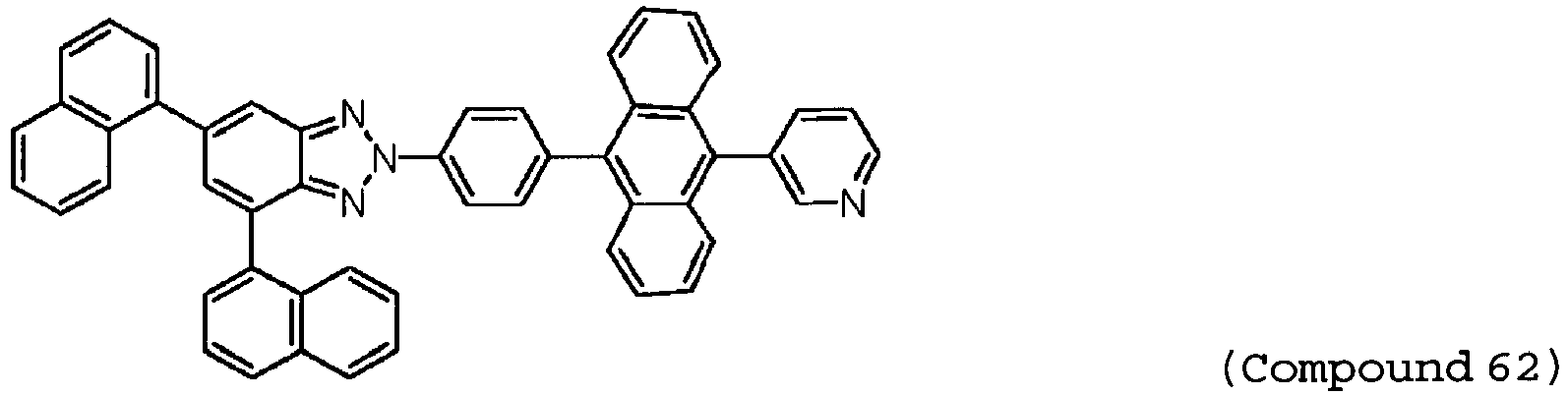
Fig. 5 ] is a 1H-NMR chart of a compound (compound 62) of Example 5. - [
Fig. 6 ] is a 1H-NMR chart of a compound (compound 63, not forming part of the invention)) of Example 6. - [
Fig. 7 ] is a view illustrating the structure of layers of an organic EL device of the present invention. - The benzotriazole derivatives of the present invention are represented by the structures in
claim 1. - Described below are the benzotriazole derivatives of the invention.


- The above-mentioned benzotriazole derivatives of the present invention have high melting points and high glass transition points (Tg), are capable of forming thin films having excellent heat resistance and are capable of maintaining amorphous state with stability. Besides, these compounds permit electrons to drift faster than the conventional electron-transporting materials, have excellent hole-blocking power, remain stable in the state of thin films and, therefore, can be used for fabricating an organic EL device that features elongated service life.
- The hole-blocking power of the benzotriazole derivatives of the invention can be evaluated in terms of work functions. As also demonstrated in Examples appearing later, the work functions are measured by forming a thin film of 100 nm on an ITO substrate and by using an ionization potential-measuring apparatus (model PYS-202 manufactured by Sumitomo Heavy Industries, Ltd.).
- The organic EL device having the organic layer formed by using the above benzotriazole derivative of the present invention has a structure as shown, for example, in
Fig. 7 . - Namely, a transparent anode 2, a hole injection layer 3, a hole-transporting layer 4, a
luminous layer 5, a hole-blocking layer 6, an electron-transportinglayer 7, anelectron injection layer 8 and acathode 9 are formed on a glass substrate 1 (which may be any transparent substrate such as transparent resin substrate or the like substrate). - The organic EL device to which the benzotriazole derivative of the present invention is applied is not limited to the one of the above layer structure, as a matter of course, and an electron-blocking layer and the like can be formed between the hole-transporting layer 4 and the
luminous layer 5. Or the organic EL device may have a simplified layer structure omitting theelectron injection layer 8 or the hole injection layer 3. For instance, some layers can be omitted from the above multilayer structure. For instance, the organic EL device can be fabricated in a simple layer structure having the anode 2, hole-transporting layer 4,luminous layer 5, electron-transportinglayer 7 andcathode 9 formed on thesubstrate 1. - That is, the benzotriazole derivative of the invention is preferably used as a material for forming organic layers (e.g. ,
luminous layer 5, hole-blocking layer 6, electron-transportinglayer 7 and electron injection layer 8) between the anode 2 and thecathode 9. - In the organic EL device, the transparent anode 2 may be formed by using an electrode material which has been known per se, i.e., by vapor-depositing an electrode material having a large work function, such as ITO or gold on the substrate 1 (transparent substrate such as glass substrate or the like).
- Further, the hole injection layer 3 can be formed on the transparent anode 2 by using the materials that have been known per se, such as those described below.
- Porphyrin compound as represented by copper phthalocyanine;
Triphenylamine derivative of the star burst type;
Arylamine having a structure coupled via a single bond or a divalent group without hetero atom (e.g., trimer or tetramer of triphenylamine);
Acceptor-type heterocyclic compounds such as hexacyanoazatriphenylene; and
High molecular materials of the application type, such as poly(3,4-ethylenedioxythiophene) (PEDOT), poly(styrene sulfonate) (PSS), etc. - The layer (thin film) can be formed by using the above materials relying not only upon the vacuum evaporation method but also upon the known methods such as spin-coating method or ink-jet method. The layers described below, too, can similarly be formed by the vacuum evaporation, the spin-coating or the ink-jet method.
- The hole-transporting layer 4, too, can be formed on the hole injection layer 3 by using a hole-transporting material that has been known per se. Representative examples of the hole-transporting materials are:
- benzidine derivatives such as,
N,N'-diphenyl-N,N'-di(m-tolyl)benzidine (hereinafter abbreviated as TPD); N,N'-diphenyl-N,N'-di(a-naphthyl)benzidine (hereinafter abbreviated as NPD); and N,N,N',N'-tetrabiphenylylbenzidine; and - amine derivatives such as,
1,1-bis[4-(di-4-tolylamino)phenyl] cyclohexane (hereinafter abbreviated as TAPC);
various triphenylamine trimers and tetramers; and the above-mentioned application-type high molecular materials that can also be used for forming the hole injection layer. - The compounds for forming the hole-transporting layer may be used alone to form a film or may be used being mixed together in two or more kinds to form a film. Or the above compounds may be used in one kind or in a plurality of kinds to form a plurality of layers, and a multiplicity of films formed by laminating such layers may be used as a hole-transporting layer.
- It is, further, allowable to form a layer that serves as both the hole injection layer 3 and the hole-transporting layer 4. The hole injection transporting layer can be formed by being coated with a high molecular material such as poly(3,4-ethylenedioxythiophene) (hereinafter abbreviated as PEDOT) or polystyrene sulfonate (hereinafter abbreviated as PSS) .
- In forming the hole-transporting layer 4 (the same holds for the hole injection layer 3, too), the material usually used for forming the layer may, further, be P-doped with a trisbromophenylaminehexachloroantimony or the like. It is also allowable to form the hole-transporting layer 4 (or the hole injection layer 3) by using a high molecular compound having a basic skeleton of TPD.
- Further, as the electron-blocking layer (that canbe formed between the hole-transporting layer 4 and the luminous layer 5) that has not been shown, there can be used a known electron-blocking compound having the electron-blocking action, such as carbazole derivative or a compound that has a triphenylsilyl group and a triarylamine structure. Described below are concrete examples of the carbazole derivative and the compound having the triarylamine structure.
- 4,4',4"-Tri(N-carbazolyl)triphenylamine (hereinafter abbreviated as TCTA);
9,9-Bis[4-(carbazole-9-il)phenyl]fluorene;
1,3-Bis(carbazole-9-il)benzene (hereinafter abbreviated as mCP); and
2,2-Bis(4-carbazole-9-ilphenyl)adamantane (hereinafter abbreviated as Ad-Cz); - 9-[4-(Carbazole-9-il)phenyl]-9-[4-(triphenylsilyl) phenyl]-9H-fluorene;
The electron-blocking layer is formed by using one, two or more kinds of the above known electron-blocking materials. It is also allowable to form a plurality of layers by using one or a plurality of kinds of the electron-blocking materials, and use a multiplicity of films formed by laminating such layers as the electron-blocking layer. - The
luminous layer 5 of the organic EL device can be formed by using the benzotriazole derivative of the invention as the luminous material. Theluminous layer 5 can also be formed by using luminous materials such as a metal complex of a quinolynol derivative as represented by Alq3, various metal complexes such as of zinc, beryllium and aluminum, anthracene derivatives, bisstyrylbenzene derivatives, pyrene derivatives, oxazole derivatives and polyparaphenylenevinylene derivatives. - It is also allowable to constitute the
luminous layer 5 by using a host material and a dopant material. - As the host material in this case, there canbe used thiazole derivative, benzimidazole derivative and polydialkylfluorene derivative in addition to the above luminous materials.
- As the dopant material, there can be used quinacridone, cumalin, rubrene, perylene and derivatives thereof, benzopyran derivatiive, rhodamine derivative and aminostyryl derivative.
- The
luminous layer 5, too, can be formed in a single-layer structure by using one or two or more kinds of the luminous materials, or in a multi-layer structure by laminating a plurality of layers. - It is, further, allowable to form the
luminous layer 5 by using a phosphorescent luminous material as the luminous material. - As the phosphorescent luminous material, there can be used a phosphorescent luminous body of a metal complex such as of iridium or platinum. For example, there can be used a green luminous phosphor such as Ir(ppy)3, a blue luminous phosphor such as Flrpic or Flr6, and a red luminous phosphor such as Btp2lr(acac). These phosphorescent luminous materials are used by being doped in the hole injection transporting host material or in the electron-transporting host material.
- As the hole injection transporting host material, there can be used carbazole derivatives such as 4,4'-di(N-carbazolyl)biphenyl (hereinafter abbreviated as CBP), TCTA or mCP in addition to using the benzotriazole derivative of the present invention.
- As the electron-transporting host material, there can be used p-bis (triphenylsilyl) benzene (hereinafter abbreviated as UGH2) or 2,2',2"-(1,3,5-phenylene)-tris (1-phenyl-1H-benzimidazole) (hereinafter abbreviated as TPBI) .
- To avoid the concentration quenching, the host material is desirably doped with the phosphorescent luminous material in an amount in a range of 1 to 30% by weight relative to the whole luminous layer relying on the vacuum coevaporation.
- As the luminous material, further, it is also allowable to use a material that emits retarded fluorescence, such as CDCB derivative like PIC-TRZ, CC2TA, PXZ-TRZ or 4CzlPN (see Appl. Phys. Let., 98, 083302 (2011)).
- The hole-blocking layer 6 can also be formed between the
luminous layer 5 and the electron-transportinglayer 7 by using a known compound having the hole-blocking action in addition to using the benzotriazole derivative of the present invention. - As the known compounds having the hole-blocking action, there can be exemplified the following compounds.
- Phenanthroline derivatives such as bathocuproin (hereinafter abbreviated as BCP) and the like;
Metal complexes of quinolinol derivatives such as aluminum(III)bis(2-methyl-8-quinolinato)-4-phenylphenolate (hereinafter abbreviated as BAlq) and the like;
Various rare earth complexes;
Triazole derivatives;
Triazine derivatives; and
Oxadiazole derivatives. - These materials can also be used for forming the electron-transporting
layer 7 that will be described below. Moreover, the hole-blocking layer 6 and the electron-transportinglayer 7 can be formed as one layer. - The hole-blocking layer 6, too, can be formed in the structure of a single layer or of a laminate of a multiplicity of layers, the layers being formed by using one kind or two or more kinds of the above-mentioned compounds having hole-blocking action.
- The electron-transporting
layer 7 can be formed by using electron-transporting compounds that have been known per se. such as metal complexes of quinolinol derivatives like Alq3 and BAlq, various metal complexes, triazole derivatives, triazine derivatives, oxadiazole derivatives, thiadiazole derivatives, carbodiimide derivatives, quinoxaline derivatives, phenanthroline derivatives and silole derivatives in addition to using the benzotriazole derivatives of the present invention. - The electron-transporting
layer 7, too, can be formed in the structure of a single layer or of a laminate of a multiplicity of layers, the layers being formed by using one kind or two or more kinds of the above-mentioned electron-transporting compounds. - The
electron injection layer 8, too, can be formed by using known compounds, i.e., by using alkali metal salts such as lithium fluoride and cesium fluoride, alkaline earth metal salts such as magnesium fluoride, and metal oxides such as aluminum oxide in addition to using the benzotriazole derivatives of the present invention. - Further, the
electron injection layer 8 or the electron-transportinglayer 7 may be formed by using materials that have usually been used for forming these layers but that are N-doped with a metal such as cesium or the like. - As the
cathode 9 of the organic EL device, there can be used an electrode material having a low work function, such as aluminum, or an electrode material of an alloy having a lower work function, such as magnesium-silver alloy, magnesium-indium alloy or aluminum-magnesium alloy. - The organic EL device forming at least one of the organic layers (e.g.,
electron injection layer 8, electron-transportinglayer 7, hole-blocking layer 6 or luminous layer 5) by using the benzotriazole derivative of the present invention, features a high luminous efficiency, a high power efficiency, a low practical driving voltage, a low luminance start voltage and very excellent durability. - The invention will now be more concretely described by way of Examples.
-

- The ingredients of the following recipe:
1-Bromo-4-nitrobenzene 50 g, (Isoquinoline-4-il)boronic acid pinacol ester 69.4 g, 2M Potassium carbonate aqueous solution 309 ml, Toluene 200 ml, Ethanol 40 ml and Tetrakistriphenylphosphine palladium (0) 11.0 g - Next, the ingredients of the following recipe:
4-(4-Nitrophenyl) isoquinoline obtained above 5.0 g, 4-Bromo-1,2-diaminobenzene 3.7 g, Caustic soda 1.6 g and Toluene 50 ml - Further, the ingredients of the following recipe:
5-Bromo-2-{4-(isoquinoline-4-il)phenylazo} phenylamine obtained above 4.0 g, Iodobenzene diacetate 4.8 g and Toluene 100 ml - Next, the ingredients of the following recipe:
5-Bromo-2-{4-(isoquinoline-4-il)phenyl}-2H-benzotriazole 4.0 g, (9,10-Diphenylanthracene-2-il) boric acid 4.5 g, 2M Potassium carbonate aqueous solution 15 ml, Toluene 30 ml, Ethanol 12 ml and Tetrakistriphenylphosphine palladium (0) 0.1 g - The obtained yellow powder was identified for its structure by the NMR.
Fig. 1 shows the results of the 1H-NMR measurement. - The following 30 signals of hydrogen were detected by the 1H-NMR (CDCl3).
δ (ppm) = 9.31 (1H)
8.56 (1H)
8.52 (1H)
8.10 (1H)
8.08 (1H)
8.03 (1H)
7.98 (1H)
7.95 (1H)
7.85 (1H)
7.74 - 7.53 (18H)
7.37 (1H)
7.43 (1H)
7.35 (1H) -

- The ingredients of the following recipe:
1-Bromo-4-nitrobenzene 50 g, (Quinoline-3-il)boronic acid 47.1 g, 2M Potassium carbonate aqueous solution 309 ml, Toluene 200 ml, Ethanol 40 ml and Tetrakistriphenylphosphine palladium (0) 11.0 g - Next, the ingredients of the following recipe:
3-(4-Nitrophenyl)quinoline obtained above 5.0 g, 4-Bromo-1,2-diaminobenzene 3.7 g, Caustic soda 1.6 g and Toluene 50 ml - Further, the ingredients of the following recipe:
5-Bromo-2-{4-(quinoline-3-il)phenylazo}phenylamine obtained above 4.0 g, Iodobenzene diacetate 4.8 g and Toluene 100 ml - Next, the ingredients of the following recipe:
5-Bromo-2-{4-(quinoline-3-il)phenyl}-2H-benzotriazole obtained above 4.0 g, (9,10-Diphenylanthracene-2-il) boric acid 4.5 g, 2M Potassium carbonate aqueous solution 15 ml, Toluene 30 ml, Ethanol 12 ml and Tetrakistriphenylphosphine palladium (0) 0.1 g - The obtained yellow powder was identified for its structure by the NMR.
Fig. 2 shows the results of the 1H-NMR measurement. - The following 30 signals of hydrogen were detected by the 1H-NMR (CDCl3).
δ (ppm) = 9.31 (1H)
8.56 (1H)
8.52 (2H)
8.10 (1H)
8.08 (1H)
8.03 (1H)
7.98 (1H)
7.96 (1H)
7.85 (1H)
7.73 - 7.53 (18H)
7.37 (1H)
7.35 (1H) -

- The ingredients of the following recipe:
5-Bromo-2-{4-(isoquinoline-4-il)phenyl}-2H-benzotriazole synthesized in Example 1 4.0 g, {9,10-Di(naphthalene-2-il}anthracene-2-il)boronic acid 5.6 g, 2M Potassium carbonate aqueous solution 15 ml, Toluene 30 ml and Ethanol 12 ml - Next, 0.1 g of the tetrakistriphenylphosphine palladium (0) was added thereto, and the mixture was heated and refluxed for 10.5 hours with stirring. The organic layer was picked up by the separating operation, was concentrated under a reduced pressure and was refined by the column chromatography to obtain 6.6 g of a yellow powder of 4-[4-[5-{9,10-di(naphthalene-2-il) anthracene-2-il}benzotriazole-2-il]phenyl]isoquinoline (compound 14) (yield 88.5%).
- The obtained yellow powder was identified for its structure by the NMR.
Fig. 3 shows the results of the 1H-NMR measurement. - The following 34 signals of hydrogen were detected by the 1H-NMR (CDCl3).
δ (ppm) = 9.29 (1H)
8.47 (2H)
8.13 (1H)
8.08 (1H)
8.06 - 8.05 (8H)
7.96 (1H)
7.91 (1H)
7.90 (1H)
7.76 (1H)
7.71 - 7.61 (15H)
7.73 (2H) -

- The ingredients of the following recipe:
5-Bromo-2-{4-(quinoline-3-il)phenyl}-2H-benzotriazole synthesized in Example 2 4.0 g, {9,10-Di(naphthalene-2-il}anthracene-2-il)boronic acid 5.6 g, 2M Potassium carbonate aqueous solution 15 ml, Toluene 30 ml and Ethanol 12 ml - Next, 0.1 g of the tetrakistriphenylphosphine palladium (0) was added thereto, and the mixture was heated and refluxed for 10.5 hours with stirring. The organic layer was picked up by the separating operation, was concentrated under a reduced pressure and was refined by the column chromatography to obtain 6.7 g of a yellow powder of 3-[4-[5-{9,10-di(naphthalene-2-il) anthracene-2-il}benzotriazole-2-il]phenyl] quinoline (compound 15) (yield 89.8%).
- The obtainedyellowpowder was identified for its structure by the NMR.
Fig. 4 shows the results of the 1H-NMR measurement. - The following 34 signals of hydrogen were detected by the 1H-NMR (CDCl3).
δ (ppm) = 9.24 (1H)
8.49 (2H)
8.39 (1H)
8.17 (1H)
8.15 (1H)
8.13 (1H)
8.08 - 8.06 (6H)
7.97 (1H)
7.96 (1H)
7.92 (1H)
7.89 (4H)
7.78 - 7.60 (12H)
7.35 (2H) -

- The ingredients of the following recipe:
5-Bromo-2-(4-chlorophenyl)-2H-benzotriazole 5.0 g, 4-Biphenylboronic acid 3.9 g, 2M Potassium carbonate aqueous solution 25 ml, 1,4-Dioxane 50 ml and Tetrakistriphenylphosphine palladium (0) 0.2 g - Next, the ingredients of the following recipe:
5-(Biphenyl-4-il)-2-(4-chlorophenyl)-2H-benzotriazole obtained above 2.8 g, Bis(pinacholato) diboron 2.2 g, Potassium acetate 2.1 g and 1,4-Dioxane 56 ml - Next, 0.16 g of a dichloromethane complex of [1,1'-bis(diphenylphosphino)ferrocene] palladium (II) dichloride (1:1) was added thereto, and the mixture was heated and stirred at 80°C for 3 hours. The mixture was cooled down to room temperature, was concentrated and was refined by adsorption by using 100 ml of toluene and 50 g of silica gel. Next, through the dispersion washing with 100 ml of methanol, there was obtained 3.0 g of a white powder of 5-(biphenyl-4-il)-2-{4-(4,4,5,5-tetramethyl-[1,3,2]dioxaborolane-2-il)phenyl}-2 H-benzotriazole crystals (yield, 54.3%).
- Next, the ingredients of the following recipe:
5-(Biphenyl-4-il)-2-{4-(4,4,5,5-tetramethyl-[1,3,2] dioxaborolane-2-il)phenyl}-2H-benzotriazole obtained above 1.0 g, 10-(Pyridine-3-il)-9-bromoanthracene 0.7 g, 2M Potassium carbonate aqueous solution 3.3 ml, 1,4- Dioxane 10 ml and Tetrakistriphenylphosphine palladium (0) 0.02 g - The obtained faintly yellow powder of crystals was identified for its structure by the NMR.
Fig. 5 shows the results of the 1H-NMR measurement. - The following 28 signals of hydrogen were detected by the 1H-NMR (CDCl3).
δ (ppm) = 8.85 (1H)
8.76 (1H)
8.64 (2H)
8.22 (1H)
8.09 (1H)
7.86 - 7.60 (15H)
7.49 (2H)
7.42 - 7.39 (5H) -
- The ingredients of the following recipe:
4,6-Dibromo-2-(4-chlorophenyl)-2H-benzotriazole 25.0 g, 1-Naphthylboronic acid 25.0 g, 2M Potassium carbonate aqueous solution 96 ml, 1,4-Dioxane 250 ml and Tetrakistriphenylphosphine palladium (0) 0.74 g - Next, the ingredients of the following recipe:
4,6-Di(naphthalene-1-il)-2-(4-chlorophenyl)-2H-benzotriazole obtained above 12.0 g, Bis(pinacholato) diboron 9.5 g, Potassium acetate 7.4 g and 1,4-Dioxane 240 ml - Next, 0.46 g of a dichloromethane complex of [1,1'-bis(diphenylphosphino)ferrocene] palladium (II) dichloride (1:1) was added thereto, and the mixture was heated and stirred at 90°C for 5 hours. The mixture was cooled down to room temperature, was concentrated and was refined by the column chromatography to obtain 9.5 g of a faintly yellow powder of 4,6-di(naphthalene-1-il)-2-{4-(4,4,5,5-tetramethyl-[1,3,2]dioxaborolane-2-il)phenyl}-2H-benzotriazole crystals (yield, 66.6%).
- Next, the ingredients of the following recipe:
4,6-Di(naphthalene-1-il)-2-{4-(4,4,5,5-tetramethyl-[1,3,2]dioxaborolane-2-il)phenyl}-2H-benzotriazole obtained above 5.7 g, 10-(Pyridine-3-il)-9-bromoanthracene 3.3 g, Potassium phosphate 6.4 g, Water 14.2 ml and 1,4-Dioxane 142 ml - Next, 0.2 g of trisdibenzylideneacetonedipalladium and 0.1 g of tricyclohexylphosphine were added thereto, and the mixture was heated and refluxed for 4 hours with stirring. The mixture was cooled, 100 ml of toluene was added thereto, insoluble matters were removed by filtration, and the product was refined by adsorption by using 15 g of NH silica gel.
- After concentrated, 50 ml of methanol was added, and the precipitated coarse product was picked up by filtration. There was obtained 5.4 g of a faintly yellow powder of 4,6-di (naphthalene-1-il)-2-[4-{10-(pyridine-3-il)anthracene-9-il} phenyl]-2H-benzotriazole (compound 62) crystals (yield, 77.7%).
- The obtained faintly yellow powder of crystals was identified for its structure by the NMR.
Fig. 6 shows the results of the 1H-NMR measurement. - The following 32 signals of hydrogen were detected by the 1H-NMR (CDCl3).
δ (ppm) = 8.84 (1H)
8.74 (1H)
8.56 (2H)
8.19 (1H)
8.15 (1H)
8.04 (1H)
7.94 (4H)
7.84 (2H)
7.76 - 7.74 (3H)
7.68 - 7.48 (12H)
7.41 - 7.37 (4H) - By using a highly sensitive differential scanning calorimeter (DSC3100S manufactured by Bruker AXS K.K.), the compounds of the present invention obtained in the above Examples 1 to 6, with the compounds of Examples 1 and 2 not forming part of the invention, were measured for their melting points and glass transition points. The results were as follows:
Melting points Glass transition points Compound of Ex. 1 286°C 153°C Compound of Ex. 2 334°C 150°C Compound of Ex. 3 238°C 183°C Compound of Ex. 4 340°C 182°C Compound of Ex. 5 318°C not observed Compound of Ex. 6 205°C 174°C - As will be understood from the above results, the compounds of the present invention have glass transition points which are not lower than 100°C and, specifically, not lower than 150°C, or which are not observed indicating that the thin films formed by using the compounds of the invention remain stable.
- Moreover, the compounds have high melting points and large heat resistances. Specifically, the compounds of Examples 1 to 5 have differences between the melting points and the glass transition points of not less than 30°C and are easy to handle.
- By using the compounds obtained in Examples 1 to 6, with the compounds of Examples 1 and 2 not forming part of the invention, films were vapor-deposited in a thickness of 100 nm on an ITO substrate and were measured for their work functions by using an apparatus for measuring ionization potentials (Model PYS-202 manufactured by Sumitomo Heavy Industries, Ltd.). The results were as follows:
Work functions Compound of Ex. 1 5.91 eV Compound of Ex. 2 5.94 eV Compound of Ex. 3 5.85 eV Compound of Ex. 4 5.91 eV Compound of Ex. 5 6.22 eV Compound of Ex. 6 6.21 eV - As described above, the compounds of the present invention have values larger than a work function of 5.5 eV possessed by general hole-transporting materials such as NPD, TPD and the like, and have large hole-blocking powers.
- An organic EL device of a structure shown in
Fig. 7 was fabricated in a manner as described below by using the compound obtained in Example 1. - First, a
glass substrate 1 on which the ITO film has been formed in a thickness of 150 nm was washed with an organic solvent and was, thereafter, washed for its surfaces by an oxygen plasma treatment. - Thereafter, the glass substrate with the ITO electrode was placed in a vacuum evaporation machine, and the pressure therein was reduced down to 0.001 Pa or lower. Next, as the hole injection layer 3, a compound HIM-1 of the following structural formula was vapor-deposited at a deposition rate of 6 nm/min. in a thickness of 20 nm so as to cover the transparent anode 2.

- Next, on the hole injection layer 3, a compound HTM-1 of the following structural formula was vapor-deposited as the hole-transporting layer 4 at a deposition rate of 6 nm/min. in a thickness of 40 nm.

- On the hole-transporting layer 4 formed above, the
luminous layer 5 was formed in a thickness of 30 nm by two-way-depositing a compound EMD-1 of the following structural formula and a compound EMH-1 of the following structural formula at a deposition rate of EMD-1:EMH-1 = 5:95.

- On the
luminous layer 5, the compound 12 synthesized in Example 1 was vapor-deposited at a deposition rate of 6 nm/min. in a thickness of 30 nm so as to work as both the hole-blocking layer 6 and the electron-transportinglayer 7. - Next, on the thus formed hole-blocking layer / electron-transporting
layer 6 and 7, theelectron injection layer 8 was formed in a thickness of 0.5 nm by vapor-depositing lithium fluoride at a deposition rate of 0.6 nm/min. - Finally, aluminum was vapor-deposited in a thickness of 150 nm to form the
cathode 9. The thus fabricated organic EL device was measured for its properties in the atmosphere at normal temperature. - The thus fabricated organic EL device was impressed with a DC voltage to measure the luminous properties which were as collectively shown in Table 1.
- An organic EL device was fabricated in the same manner as in Example 9 but using the compound (compound 13) of Example 2 instead of using the compound (compound 12) of Example 1 to form the hole-blocking layer/electron-transporting layer in a thickness of 30 nm. The organic EL device was measured for its properties in the atmosphere at normal temperature.
- The organic EL device was impressed with a DC voltage to measure the luminous properties which were as collectively shown in Table 1.
- An organic EL device was fabricated in the same manner as in Example 9 but using the compound (compound 14) of Example 3 instead of using the compound (compound 12) of Example 1 to form the hole-blocking layer/electron-transporting layer in a thickness of 30 nm. The thus fabricated organic EL device was measured for its properties in the atmosphere at normal temperature.
- The thus fabricated organic EL device was impressed with a DC voltage to measure the luminous properties which were as collectively shown in Table 1.
- An organic EL device was fabricated in the same manner as in Example 9 but using the compound (compound 15) of Example 4 instead of using the compound (compound 12) of Example 1 to form the hole-blocking layer/electron-transporting layer in a thickness of 30 nm. The thus fabricated organic EL device was measured for its properties in the atmosphere at normal temperature.
- The thus fabricated organic EL device was impressed with a DC voltage to measure the luminous properties which were as collectively shown in Table 1.
- An organic EL device was fabricated in the same manner as in Example 9 but using the compound (compound 62) of Example 6 instead of using the compound (compound 12) of Example 1 to form the hole-blocking layer/electron-transporting layer in a thickness of 30 nm. The thus fabricated organic EL device was measured for its properties in the atmosphere at normal temperature.
- The thus fabricated organic EL device was impressed with a DC voltage to measure the luminous properties which were as collectively shown in Table 1.
- An organic EL device was fabricated in the same manner as in Example 9 but using the compound (ETM-1) of the following structural formula instead of using the compound (compound 12) of Example 1 to form the hole-blocking layer / electron-transporting layer in a thickness of 30 nm. The thus fabricated organic EL device was measured for its properties in the atmosphere at normal temperature. The thus fabricated organic EL device was impressed with a DC voltage to measure the luminous properties which were as collectively shown in Table 1.

Table 1 Compound Voltage [V] (@10 mA/cm2) Brightness [cd/m2] (@10 mA/cm2) Current efficiency [cd/A] (@10 mA/cm2) Power efficiency [lm/W] (@ 10 mA/cm2) Example 9 compound 12 4.95 832 8.32 5.28 Example 10 compound 13 5.03 836 8.36 5.22 Example 11 compound 14 5.05 845 8.45 5.25 Example 12 compound 15 5.10 843 8.43 5.19 Example 13 compound 62 4.98 840 8.40 5.21 Comp. Ex. 1 ETM-1 5.95 792 7.92 4.19 - As for the driving voltage at a current density of 10 mA/cm2 as shown in Table 1, the organic EL devices of Examples to 13 of the invention have driving voltages of as low as 4.95 to 5.10 V as compared to 5.95 V of the organic EL device of Comparative Example 1 that uses the ETM-1 of the above structural formula. Further, the organic EL devices of Examples 9 to 13 of the invention exhibit current efficiencies of 8.32 to 8.45 cd/A which are great improvements over 7.92 cd/A of the organic EL device of Comparative Example 1.
- Moreover, the organic EL devices of Examples 11 to 13 of the invention exhibit power efficiencies of 5.19 to 5.28 lm/W which are great improvements over 4.19 lm/W of the organic EL device of Comparative Example 1.
- It will, therefore, be learned that the organic EL devices of the present invention are capable of achieving a great decrease in the practical driving voltages and great improvement in the luminous efficiency and power efficiency as compared to the devices that use the ETM-1 of the above structural formula that has been generally used as an electron-transporting material.
- From a conspicuous decrease in the driving voltages attained by the organic EL devices using the benzotriazole derivatives of the present invention, it is presumed that the rate of electron migration in the benzotriazole derivatives is very larger than that of the ETM-1 of the above structural formula that is a widely used electron-transporting material.
- The benzotriazole derivatives of the present invention have good electron injection property and excellent hole-blocking power, remain stable in their thin film state, and can be used as excellent compounds for fabricating the organic EL devices. Upon fabricating the organic EL devices by using the above compounds, further, it is allowed to attain a high luminous efficiency and power efficiency while lowering the practical driving voltage and improving the durability. Their use can, therefore, be expanded to, for example, domestic appliances and illumination equipment.
-
- 1
- glass substrate
- 2
- transparent anode
- 3
- hole injection layer
- 4
- hole-transporting layer
- 5
- luminous layer
- 6
- hole-blocking layer
- 7
- electron-transporting layer
- 8
- electron injection layer
- 9
- cathode
Claims (3)
- A benzotriazole derivative represented by one of the following formulae:


- An organic electroluminescent device having a pair of electrodes and at least one organic layer held therebetween, wherein at least the one organic layer contains the benzotriazole derivative of claim 1.
- The organic electroluminescent device according to claim 2, wherein the at least one organic layer is an electron-transporting layer, a hole-blocking layer, a luminous layer or an electron injection layer.
Applications Claiming Priority (2)
| Application Number | Priority Date | Filing Date | Title |
|---|---|---|---|
| JP2013156295 | 2013-07-29 | ||
| PCT/JP2014/069574 WO2015016135A1 (en) | 2013-07-29 | 2014-07-24 | Benzotriazole derivative and organic electroluminescent element |
Publications (3)
| Publication Number | Publication Date |
|---|---|
| EP3029034A1 EP3029034A1 (en) | 2016-06-08 |
| EP3029034A4 EP3029034A4 (en) | 2017-03-29 |
| EP3029034B1 true EP3029034B1 (en) | 2021-04-14 |
Family
ID=52431671
Family Applications (1)
| Application Number | Title | Priority Date | Filing Date |
|---|---|---|---|
| EP14832687.9A Active EP3029034B1 (en) | 2013-07-29 | 2014-07-24 | Benzotriazole derivatives and organic electroluminescent element |
Country Status (7)
| Country | Link |
|---|---|
| US (1) | US9842999B2 (en) |
| EP (1) | EP3029034B1 (en) |
| JP (1) | JP6389461B2 (en) |
| KR (1) | KR102214289B1 (en) |
| CN (2) | CN105579443A (en) |
| TW (1) | TWI637039B (en) |
| WO (1) | WO2015016135A1 (en) |
Families Citing this family (4)
| Publication number | Priority date | Publication date | Assignee | Title |
|---|---|---|---|---|
| WO2015156325A1 (en) * | 2014-04-10 | 2015-10-15 | 保土谷化学工業株式会社 | Quinolinotriazole derivative and organic electroluminescent element |
| KR101774900B1 (en) * | 2015-03-25 | 2017-09-05 | (주)부흥산업사 | Preparing method of aromatic triazine derivatives for organic electroluminescent device |
| CN107534093B (en) * | 2015-04-27 | 2020-06-30 | 保土谷化学工业株式会社 | Organic electroluminescent device |
| JP2016213469A (en) * | 2015-05-11 | 2016-12-15 | 保土谷化学工業株式会社 | Organic electroluminescent element |
Citations (1)
| Publication number | Priority date | Publication date | Assignee | Title |
|---|---|---|---|---|
| WO2013054764A1 (en) * | 2011-10-14 | 2013-04-18 | 保土谷化学工業株式会社 | New benzotriazole derivative and organic electroluminescent element in which said derivative is used |
Family Cites Families (11)
| Publication number | Priority date | Publication date | Assignee | Title |
|---|---|---|---|---|
| DE2636090A1 (en) * | 1976-08-11 | 1978-02-16 | Bayer Ag | BIS-BENZOXAZOLYL COMPOUNDS |
| WO1994022974A1 (en) | 1993-03-26 | 1994-10-13 | Sumitomo Electric Industries, Ltd. | Organic electroluminescent elements |
| JP2734341B2 (en) | 1993-03-26 | 1998-03-30 | 住友電気工業株式会社 | Organic electroluminescence device |
| KR100691543B1 (en) | 2002-01-18 | 2007-03-09 | 주식회사 엘지화학 | New material for electron transport and organic light emitting device using the same |
| CN100502087C (en) | 2002-06-06 | 2009-06-17 | 西巴特殊化学品控股有限公司 | Electroluminescent device |
| WO2005054212A2 (en) * | 2003-12-05 | 2005-06-16 | Ciba Specialty Chemicals Holding Inc. | Electroluminescent device |
| JP2008218986A (en) | 2007-02-06 | 2008-09-18 | Sumitomo Chemical Co Ltd | Composition and light-emitting device using the composition |
| CN102356076A (en) * | 2009-03-18 | 2012-02-15 | 保土谷化学工业株式会社 | Compounds with benzotriazole ring structure and organic electroluminescent devices |
| KR101866851B1 (en) * | 2010-12-24 | 2018-06-14 | 에스에프씨 주식회사 | Heterocyclic compounds and organic light-emitting diode including the same |
| WO2013049062A2 (en) * | 2011-09-26 | 2013-04-04 | Nitto Denko Corporation | Highly-fluorescent and photo-stable chromophores for enhanced solar harvesting efficiency |
| KR101499356B1 (en) * | 2013-06-28 | 2015-03-05 | 주식회사 엘지화학 | Hetero-cyclic compound and organic light emitting device comprising the same |
-
2014
- 2014-07-24 KR KR1020167004897A patent/KR102214289B1/en active Active
- 2014-07-24 JP JP2015529544A patent/JP6389461B2/en active Active
- 2014-07-24 CN CN201480053578.1A patent/CN105579443A/en active Pending
- 2014-07-24 WO PCT/JP2014/069574 patent/WO2015016135A1/en not_active Ceased
- 2014-07-24 EP EP14832687.9A patent/EP3029034B1/en active Active
- 2014-07-24 US US14/908,310 patent/US9842999B2/en not_active Expired - Fee Related
- 2014-07-24 CN CN202011038029.0A patent/CN112079814B/en active Active
- 2014-07-29 TW TW103125862A patent/TWI637039B/en active
Patent Citations (2)
| Publication number | Priority date | Publication date | Assignee | Title |
|---|---|---|---|---|
| WO2013054764A1 (en) * | 2011-10-14 | 2013-04-18 | 保土谷化学工業株式会社 | New benzotriazole derivative and organic electroluminescent element in which said derivative is used |
| EP2767534A1 (en) * | 2011-10-14 | 2014-08-20 | Hodogaya Chemical Co., Ltd. | New benzotriazole derivative and organic electroluminescent element in which said derivative is used |
Also Published As
| Publication number | Publication date |
|---|---|
| TWI637039B (en) | 2018-10-01 |
| KR20160039236A (en) | 2016-04-08 |
| JPWO2015016135A1 (en) | 2017-03-02 |
| EP3029034A4 (en) | 2017-03-29 |
| US9842999B2 (en) | 2017-12-12 |
| CN105579443A (en) | 2016-05-11 |
| TW201512371A (en) | 2015-04-01 |
| WO2015016135A1 (en) | 2015-02-05 |
| JP6389461B2 (en) | 2018-09-12 |
| EP3029034A1 (en) | 2016-06-08 |
| CN112079814B (en) | 2023-11-07 |
| US20160164001A1 (en) | 2016-06-09 |
| KR102214289B1 (en) | 2021-02-08 |
| CN112079814A (en) | 2020-12-15 |
Similar Documents
| Publication | Publication Date | Title |
|---|---|---|
| US20200303658A1 (en) | Pyrimidine derivative and an organic electroluminescent device | |
| EP2767534B1 (en) | New benzotriazole derivative and organic electroluminescent element in which said derivative is used | |
| US9306174B2 (en) | Organic electroluminescent device | |
| EP3309141B1 (en) | Arylamine compound and organic electroluminescent device | |
| EP2540707A1 (en) | Substituted pyridyl compound and organic electroluminescent element | |
| EP2492986A1 (en) | Organic electroluminescent element | |
| EP3664173B1 (en) | Organic electroluminescence element containing compound having benzoazole ring structure | |
| EP3683852B1 (en) | Organic electroluminescent element | |
| US12024527B2 (en) | Compound having azabenzoxazole ring structure and organic electroluminescent element | |
| US9842999B2 (en) | Benzotriazole derivative and an organic electroluminescent device | |
| EP2963032A1 (en) | Novel naphthotriazole derivative and organic electroluminescence element | |
| EP2679582A1 (en) | Compound containing substituted o-terphenyl structure, and organic electroluminescent element | |
| EP3981764A1 (en) | Compound having benzotriazole ring structure and organic electroluminescence element | |
| EP3683212B1 (en) | Compound having pyrimidine ring structure and organic electroluminescent element | |
| JP6479770B2 (en) | Quinolininotriazole derivatives and organic electroluminescence devices | |
| WO2020080341A1 (en) | Compound having pyrimidine ring structure and organic electroluminescent element |
Legal Events
| Date | Code | Title | Description |
|---|---|---|---|
| PUAI | Public reference made under article 153(3) epc to a published international application that has entered the european phase |
Free format text: ORIGINAL CODE: 0009012 |
|
| 17P | Request for examination filed |
Effective date: 20160225 |
|
| AK | Designated contracting states |
Kind code of ref document: A1 Designated state(s): AL AT BE BG CH CY CZ DE DK EE ES FI FR GB GR HR HU IE IS IT LI LT LU LV MC MK MT NL NO PL PT RO RS SE SI SK SM TR |
|
| AX | Request for extension of the european patent |
Extension state: BA ME |
|
| DAX | Request for extension of the european patent (deleted) | ||
| REG | Reference to a national code |
Ref country code: DE Ref legal event code: R079 Ref document number: 602014076640 Country of ref document: DE Free format text: PREVIOUS MAIN CLASS: C07D0401100000 Ipc: H01L0051540000 |
|
| A4 | Supplementary search report drawn up and despatched |
Effective date: 20170224 |
|
| RIC1 | Information provided on ipc code assigned before grant |
Ipc: H01L 51/54 20060101AFI20170220BHEP Ipc: C07D 401/10 20060101ALI20170220BHEP |
|
| STAA | Information on the status of an ep patent application or granted ep patent |
Free format text: STATUS: EXAMINATION IS IN PROGRESS |
|
| 17Q | First examination report despatched |
Effective date: 20200520 |
|
| GRAP | Despatch of communication of intention to grant a patent |
Free format text: ORIGINAL CODE: EPIDOSNIGR1 |
|
| STAA | Information on the status of an ep patent application or granted ep patent |
Free format text: STATUS: GRANT OF PATENT IS INTENDED |
|
| INTG | Intention to grant announced |
Effective date: 20201126 |
|
| GRAS | Grant fee paid |
Free format text: ORIGINAL CODE: EPIDOSNIGR3 |
|
| GRAA | (expected) grant |
Free format text: ORIGINAL CODE: 0009210 |
|
| STAA | Information on the status of an ep patent application or granted ep patent |
Free format text: STATUS: THE PATENT HAS BEEN GRANTED |
|
| AK | Designated contracting states |
Kind code of ref document: B1 Designated state(s): AL AT BE BG CH CY CZ DE DK EE ES FI FR GB GR HR HU IE IS IT LI LT LU LV MC MK MT NL NO PL PT RO RS SE SI SK SM TR |
|
| REG | Reference to a national code |
Ref country code: GB Ref legal event code: FG4D |
|
| REG | Reference to a national code |
Ref country code: CH Ref legal event code: EP |
|
| REG | Reference to a national code |
Ref country code: DE Ref legal event code: R096 Ref document number: 602014076640 Country of ref document: DE |
|
| REG | Reference to a national code |
Ref country code: IE Ref legal event code: FG4D |
|
| REG | Reference to a national code |
Ref country code: AT Ref legal event code: REF Ref document number: 1383247 Country of ref document: AT Kind code of ref document: T Effective date: 20210515 |
|
| REG | Reference to a national code |
Ref country code: LT Ref legal event code: MG9D |
|
| REG | Reference to a national code |
Ref country code: AT Ref legal event code: MK05 Ref document number: 1383247 Country of ref document: AT Kind code of ref document: T Effective date: 20210414 |
|
| REG | Reference to a national code |
Ref country code: NL Ref legal event code: MP Effective date: 20210414 |
|
| PG25 | Lapsed in a contracting state [announced via postgrant information from national office to epo] |
Ref country code: HR Free format text: LAPSE BECAUSE OF FAILURE TO SUBMIT A TRANSLATION OF THE DESCRIPTION OR TO PAY THE FEE WITHIN THE PRESCRIBED TIME-LIMIT Effective date: 20210414 Ref country code: NL Free format text: LAPSE BECAUSE OF FAILURE TO SUBMIT A TRANSLATION OF THE DESCRIPTION OR TO PAY THE FEE WITHIN THE PRESCRIBED TIME-LIMIT Effective date: 20210414 Ref country code: LT Free format text: LAPSE BECAUSE OF FAILURE TO SUBMIT A TRANSLATION OF THE DESCRIPTION OR TO PAY THE FEE WITHIN THE PRESCRIBED TIME-LIMIT Effective date: 20210414 Ref country code: FI Free format text: LAPSE BECAUSE OF FAILURE TO SUBMIT A TRANSLATION OF THE DESCRIPTION OR TO PAY THE FEE WITHIN THE PRESCRIBED TIME-LIMIT Effective date: 20210414 Ref country code: AT Free format text: LAPSE BECAUSE OF FAILURE TO SUBMIT A TRANSLATION OF THE DESCRIPTION OR TO PAY THE FEE WITHIN THE PRESCRIBED TIME-LIMIT Effective date: 20210414 Ref country code: BG Free format text: LAPSE BECAUSE OF FAILURE TO SUBMIT A TRANSLATION OF THE DESCRIPTION OR TO PAY THE FEE WITHIN THE PRESCRIBED TIME-LIMIT Effective date: 20210714 |
|
| PG25 | Lapsed in a contracting state [announced via postgrant information from national office to epo] |
Ref country code: NO Free format text: LAPSE BECAUSE OF FAILURE TO SUBMIT A TRANSLATION OF THE DESCRIPTION OR TO PAY THE FEE WITHIN THE PRESCRIBED TIME-LIMIT Effective date: 20210714 Ref country code: PL Free format text: LAPSE BECAUSE OF FAILURE TO SUBMIT A TRANSLATION OF THE DESCRIPTION OR TO PAY THE FEE WITHIN THE PRESCRIBED TIME-LIMIT Effective date: 20210414 Ref country code: PT Free format text: LAPSE BECAUSE OF FAILURE TO SUBMIT A TRANSLATION OF THE DESCRIPTION OR TO PAY THE FEE WITHIN THE PRESCRIBED TIME-LIMIT Effective date: 20210816 Ref country code: ES Free format text: LAPSE BECAUSE OF FAILURE TO SUBMIT A TRANSLATION OF THE DESCRIPTION OR TO PAY THE FEE WITHIN THE PRESCRIBED TIME-LIMIT Effective date: 20210414 Ref country code: RS Free format text: LAPSE BECAUSE OF FAILURE TO SUBMIT A TRANSLATION OF THE DESCRIPTION OR TO PAY THE FEE WITHIN THE PRESCRIBED TIME-LIMIT Effective date: 20210414 Ref country code: SE Free format text: LAPSE BECAUSE OF FAILURE TO SUBMIT A TRANSLATION OF THE DESCRIPTION OR TO PAY THE FEE WITHIN THE PRESCRIBED TIME-LIMIT Effective date: 20210414 Ref country code: LV Free format text: LAPSE BECAUSE OF FAILURE TO SUBMIT A TRANSLATION OF THE DESCRIPTION OR TO PAY THE FEE WITHIN THE PRESCRIBED TIME-LIMIT Effective date: 20210414 Ref country code: GR Free format text: LAPSE BECAUSE OF FAILURE TO SUBMIT A TRANSLATION OF THE DESCRIPTION OR TO PAY THE FEE WITHIN THE PRESCRIBED TIME-LIMIT Effective date: 20210715 Ref country code: IS Free format text: LAPSE BECAUSE OF FAILURE TO SUBMIT A TRANSLATION OF THE DESCRIPTION OR TO PAY THE FEE WITHIN THE PRESCRIBED TIME-LIMIT Effective date: 20210814 |
|
| REG | Reference to a national code |
Ref country code: DE Ref legal event code: R097 Ref document number: 602014076640 Country of ref document: DE |
|
| PG25 | Lapsed in a contracting state [announced via postgrant information from national office to epo] |
Ref country code: RO Free format text: LAPSE BECAUSE OF FAILURE TO SUBMIT A TRANSLATION OF THE DESCRIPTION OR TO PAY THE FEE WITHIN THE PRESCRIBED TIME-LIMIT Effective date: 20210414 Ref country code: SM Free format text: LAPSE BECAUSE OF FAILURE TO SUBMIT A TRANSLATION OF THE DESCRIPTION OR TO PAY THE FEE WITHIN THE PRESCRIBED TIME-LIMIT Effective date: 20210414 Ref country code: SK Free format text: LAPSE BECAUSE OF FAILURE TO SUBMIT A TRANSLATION OF THE DESCRIPTION OR TO PAY THE FEE WITHIN THE PRESCRIBED TIME-LIMIT Effective date: 20210414 Ref country code: CZ Free format text: LAPSE BECAUSE OF FAILURE TO SUBMIT A TRANSLATION OF THE DESCRIPTION OR TO PAY THE FEE WITHIN THE PRESCRIBED TIME-LIMIT Effective date: 20210414 Ref country code: DK Free format text: LAPSE BECAUSE OF FAILURE TO SUBMIT A TRANSLATION OF THE DESCRIPTION OR TO PAY THE FEE WITHIN THE PRESCRIBED TIME-LIMIT Effective date: 20210414 Ref country code: EE Free format text: LAPSE BECAUSE OF FAILURE TO SUBMIT A TRANSLATION OF THE DESCRIPTION OR TO PAY THE FEE WITHIN THE PRESCRIBED TIME-LIMIT Effective date: 20210414 |
|
| PLBE | No opposition filed within time limit |
Free format text: ORIGINAL CODE: 0009261 |
|
| STAA | Information on the status of an ep patent application or granted ep patent |
Free format text: STATUS: NO OPPOSITION FILED WITHIN TIME LIMIT |
|
| REG | Reference to a national code |
Ref country code: CH Ref legal event code: PL |
|
| 26N | No opposition filed |
Effective date: 20220117 |
|
| GBPC | Gb: european patent ceased through non-payment of renewal fee |
Effective date: 20210724 |
|
| PG25 | Lapsed in a contracting state [announced via postgrant information from national office to epo] |
Ref country code: MC Free format text: LAPSE BECAUSE OF FAILURE TO SUBMIT A TRANSLATION OF THE DESCRIPTION OR TO PAY THE FEE WITHIN THE PRESCRIBED TIME-LIMIT Effective date: 20210414 |
|
| REG | Reference to a national code |
Ref country code: BE Ref legal event code: MM Effective date: 20210731 |
|
| PG25 | Lapsed in a contracting state [announced via postgrant information from national office to epo] |
Ref country code: LI Free format text: LAPSE BECAUSE OF NON-PAYMENT OF DUE FEES Effective date: 20210731 Ref country code: GB Free format text: LAPSE BECAUSE OF NON-PAYMENT OF DUE FEES Effective date: 20210724 Ref country code: CH Free format text: LAPSE BECAUSE OF NON-PAYMENT OF DUE FEES Effective date: 20210731 |
|
| PG25 | Lapsed in a contracting state [announced via postgrant information from national office to epo] |
Ref country code: IS Free format text: LAPSE BECAUSE OF FAILURE TO SUBMIT A TRANSLATION OF THE DESCRIPTION OR TO PAY THE FEE WITHIN THE PRESCRIBED TIME-LIMIT Effective date: 20210814 Ref country code: LU Free format text: LAPSE BECAUSE OF NON-PAYMENT OF DUE FEES Effective date: 20210724 Ref country code: FR Free format text: LAPSE BECAUSE OF NON-PAYMENT OF DUE FEES Effective date: 20210731 Ref country code: AL Free format text: LAPSE BECAUSE OF FAILURE TO SUBMIT A TRANSLATION OF THE DESCRIPTION OR TO PAY THE FEE WITHIN THE PRESCRIBED TIME-LIMIT Effective date: 20210414 |
|
| PG25 | Lapsed in a contracting state [announced via postgrant information from national office to epo] |
Ref country code: IT Free format text: LAPSE BECAUSE OF FAILURE TO SUBMIT A TRANSLATION OF THE DESCRIPTION OR TO PAY THE FEE WITHIN THE PRESCRIBED TIME-LIMIT Effective date: 20210414 Ref country code: IE Free format text: LAPSE BECAUSE OF NON-PAYMENT OF DUE FEES Effective date: 20210724 Ref country code: BE Free format text: LAPSE BECAUSE OF NON-PAYMENT OF DUE FEES Effective date: 20210731 |
|
| PGFP | Annual fee paid to national office [announced via postgrant information from national office to epo] |
Ref country code: DE Payment date: 20220620 Year of fee payment: 9 |
|
| REG | Reference to a national code |
Ref country code: DE Ref legal event code: R079 Ref document number: 602014076640 Country of ref document: DE Free format text: PREVIOUS MAIN CLASS: H01L0051540000 Ipc: H10K0085000000 |
|
| PG25 | Lapsed in a contracting state [announced via postgrant information from national office to epo] |
Ref country code: HU Free format text: LAPSE BECAUSE OF FAILURE TO SUBMIT A TRANSLATION OF THE DESCRIPTION OR TO PAY THE FEE WITHIN THE PRESCRIBED TIME-LIMIT; INVALID AB INITIO Effective date: 20140724 |
|
| PG25 | Lapsed in a contracting state [announced via postgrant information from national office to epo] |
Ref country code: CY Free format text: LAPSE BECAUSE OF FAILURE TO SUBMIT A TRANSLATION OF THE DESCRIPTION OR TO PAY THE FEE WITHIN THE PRESCRIBED TIME-LIMIT Effective date: 20210414 |
|
| REG | Reference to a national code |
Ref country code: DE Ref legal event code: R119 Ref document number: 602014076640 Country of ref document: DE |
|
| PG25 | Lapsed in a contracting state [announced via postgrant information from national office to epo] |
Ref country code: MK Free format text: LAPSE BECAUSE OF FAILURE TO SUBMIT A TRANSLATION OF THE DESCRIPTION OR TO PAY THE FEE WITHIN THE PRESCRIBED TIME-LIMIT Effective date: 20210414 Ref country code: DE Free format text: LAPSE BECAUSE OF NON-PAYMENT OF DUE FEES Effective date: 20240201 |
|
| PG25 | Lapsed in a contracting state [announced via postgrant information from national office to epo] |
Ref country code: TR Free format text: LAPSE BECAUSE OF FAILURE TO SUBMIT A TRANSLATION OF THE DESCRIPTION OR TO PAY THE FEE WITHIN THE PRESCRIBED TIME-LIMIT Effective date: 20210414 |
|
| PG25 | Lapsed in a contracting state [announced via postgrant information from national office to epo] |
Ref country code: MT Free format text: LAPSE BECAUSE OF FAILURE TO SUBMIT A TRANSLATION OF THE DESCRIPTION OR TO PAY THE FEE WITHIN THE PRESCRIBED TIME-LIMIT Effective date: 20210414 |