EP3025425B1 - Suppression of spurious harmonics generated in tx driver amplifiers - Google Patents
Suppression of spurious harmonics generated in tx driver amplifiers Download PDFInfo
- Publication number
- EP3025425B1 EP3025425B1 EP14750265.2A EP14750265A EP3025425B1 EP 3025425 B1 EP3025425 B1 EP 3025425B1 EP 14750265 A EP14750265 A EP 14750265A EP 3025425 B1 EP3025425 B1 EP 3025425B1
- Authority
- EP
- European Patent Office
- Prior art keywords
- signal
- phases
- signals
- gain
- amplifiers
- Prior art date
- Legal status (The legal status is an assumption and is not a legal conclusion. Google has not performed a legal analysis and makes no representation as to the accuracy of the status listed.)
- Active
Links
Images


Classifications
-
- H—ELECTRICITY
- H04—ELECTRIC COMMUNICATION TECHNIQUE
- H04B—TRANSMISSION
- H04B1/00—Details of transmission systems, not covered by a single one of groups H04B3/00 - H04B13/00; Details of transmission systems not characterised by the medium used for transmission
- H04B1/02—Transmitters
- H04B1/04—Circuits
- H04B1/0483—Transmitters with multiple parallel paths
-
- H—ELECTRICITY
- H03—ELECTRONIC CIRCUITRY
- H03D—DEMODULATION OR TRANSFERENCE OF MODULATION FROM ONE CARRIER TO ANOTHER
- H03D7/00—Transference of modulation from one carrier to another, e.g. frequency-changing
- H03D7/16—Multiple-frequency-changing
- H03D7/165—Multiple-frequency-changing at least two frequency changers being located in different paths, e.g. in two paths with carriers in quadrature
-
- H—ELECTRICITY
- H03—ELECTRONIC CIRCUITRY
- H03F—AMPLIFIERS
- H03F1/00—Details of amplifiers with only discharge tubes, only semiconductor devices or only unspecified devices as amplifying elements
- H03F1/32—Modifications of amplifiers to reduce non-linear distortion
-
- H—ELECTRICITY
- H03—ELECTRONIC CIRCUITRY
- H03F—AMPLIFIERS
- H03F3/00—Amplifiers with only discharge tubes or only semiconductor devices as amplifying elements
- H03F3/189—High-frequency amplifiers, e.g. radio frequency amplifiers
-
- H—ELECTRICITY
- H03—ELECTRONIC CIRCUITRY
- H03F—AMPLIFIERS
- H03F3/00—Amplifiers with only discharge tubes or only semiconductor devices as amplifying elements
- H03F3/20—Power amplifiers, e.g. Class B amplifiers, Class C amplifiers
- H03F3/24—Power amplifiers, e.g. Class B amplifiers, Class C amplifiers of transmitter output stages
-
- H—ELECTRICITY
- H03—ELECTRONIC CIRCUITRY
- H03F—AMPLIFIERS
- H03F3/00—Amplifiers with only discharge tubes or only semiconductor devices as amplifying elements
- H03F3/60—Amplifiers in which coupling networks have distributed constants, e.g. with waveguide resonators
- H03F3/602—Combinations of several amplifiers
-
- H—ELECTRICITY
- H03—ELECTRONIC CIRCUITRY
- H03D—DEMODULATION OR TRANSFERENCE OF MODULATION FROM ONE CARRIER TO ANOTHER
- H03D2200/00—Indexing scheme relating to details of demodulation or transference of modulation from one carrier to another covered by H03D
- H03D2200/0041—Functional aspects of demodulators
- H03D2200/0086—Reduction or prevention of harmonic frequencies
-
- H—ELECTRICITY
- H03—ELECTRONIC CIRCUITRY
- H03F—AMPLIFIERS
- H03F2200/00—Indexing scheme relating to amplifiers
- H03F2200/165—A filter circuit coupled to the input of an amplifier
-
- H—ELECTRICITY
- H03—ELECTRONIC CIRCUITRY
- H03F—AMPLIFIERS
- H03F2200/00—Indexing scheme relating to amplifiers
- H03F2200/336—A I/Q, i.e. phase quadrature, modulator or demodulator being used in an amplifying circuit
Definitions
- the present disclosure relates to electronic circuits, and more particularly to a transmitter used in such circuits.
- a wireless communication device such as a cellular phone, includes a transmitter for transmitting signals and a receiver for receiving signals.
- the receiver often downconverts an analog radio frequency (RF) signal to an intermediate frequency (IF) signal which is filtered, amplified, and converted to a baseband signal.
- the transmitter converts a baseband digital signal to an analog signal, which is filtered and upconverted to an RF signal before being transmitted.
- Non-linearity in the circuit blocks coupled to the output of the upconversion mixers such as power amplifiers (PA) and driver amplifiers, often generate harmonics of the transmitted signal.
- harmonics particularly the third and fifth harmonics, are undesired and should be kept below a certain threshold in order to meet the emission requirements.
- LTE long term evolution
- such harmonics may couple to and desensitize an aggregated receiver associated with a different band when carrier aggregation is employed. Controlling the transmitter harmonics remains a challenge.
- WO 2010/089700 A1 describing a polyphase harmonic rejection mixer, comprising a plurality of stages following each other; wherein a first stage is arranged to perform at least frequency conversion; and a second stage is arranged to perform at least selective weighting and combining; wherein at least two of the plurality of stages are arranged to perform at least combining.
- the first stage comprises three single-ended gain blocks, arranged to perform selective weighting, frequency conversion and combining; and a second stage following the first stage and arranged to perform selective weighting and combining.
- the second stage may reduce the number of phases output by the first stage and may output a complex differential down converted signal.
- the mixer may be directly interfaced to an antenna of an LNA-less receiver without weighting in the first stage.
- the mixer may be included in a software-defined radio.
- a communication device in accordance with one embodiment of the present invention includes, in part, N upconverters, N amplifiers and at least one combiner.
- Each upconverter made up of either M single balanced upconversion mixers or M/2 double-balanced upconversion mixers, receives M phases of a baseband signal to be transmitted.
- Each upconverter further receives a different one of N sets of phases of a local oscillator (LO) signal.
- LO local oscillator
- Each of the N sets includes M different phases of the LO signal.
- Each amplifier is responsive to a different one of the upconverters to generate an amplified upconverted signal.
- the combiner combines the N amplified upconverted signals to generate an output signal.
- Undesired upconverted signal component at a frequency equal to a multiple of a sum of the LO signal frequency and the baseband signal frequency, or a multiple of a difference between the LO signal frequency and the baseband signal frequency is substantially suppressed from the output signal by selecting a gain of at least one of the amplifiers to be different from the gain of the remaining amplifiers.
- N and M are integers greater than 1.
- the communication device further includes, in part, a first filter receiving a baseband in-phase signal to generate a first set of filtered in-phase baseband signals to be transmitted, and a second filter receiving a baseband quadrature-phase signal to generate a second set of filtered quadrature-phase of the signals to be transmitted.
- the baseband in-phase signal includes a first pair of complementary signals and the baseband quadrature-phase signal includes a second pair of complementary signals.
- N is 3 and M is 4.
- first and second amplifiers are selected to have an equal gain and a third amplifier is selected to have a gain larger than the gain of the first and second amplifiers.
- the gain of the third amplifier is substantially 2 1 6 times the gain of the first and second amplifiers. In one embodiment, the gain of the third amplifier is substantially 2 1 10 times the gain of the first and second amplifiers.
- the four phases of the LO signal in a first set lead corresponding four phases of the LO signal in a second set by 45°.
- the four phases of the LO signal in a third set lag corresponding four phases of the LO signal in the second set by 45°.
- the four phases of the LO signal in the first are at 315, 135, 45, 225 degrees
- the 4 phases of the LO signal in the second set are at 0, 180, 90, 270 degrees
- the 4 phases of the LO signal in the third set are at 45, 225, 135, 315 degrees.
- a communication device in accordance with another embodiment of the present invention includes, in part, N sets of upconverters and N sets of combiners.
- Each of the N set of upconverters includes Q upconverters.
- Each of the Q upconverters in each of the N sets receives M phases of a signal to be transmitted.
- Each of the Q upconverters in each of the N sets further receives one of Q*N sets of phases of a LO signal.
- Each of the Q*N sets includes M phases of the LO signal.
- each of the Q upconverters generates an upconverted in-phase signal and an upconverted inverse signal.
- Each set of combiners is associated with a different one of the N sets of upconverters.
- a first combiner in each such set combines the N in-phase signals the first combiner receives from its associated upconverters.
- a second combiner in each set combines the N inverse signals the second combiner receives from its associated upconverters.
- Undesired upconverted signal component at a frequency equal to a multiple of a sum of the LO signal frequency and the baseband signal frequency, or a multiple of a difference between the LO signal frequency and the baseband signal frequency is substantially suppressed from the combined in-phase and inverse signals, Q, M and N are positive integers.
- the communication device further includes, in part, a first filter receiving a baseband in-phase signal to generate a first set of in-phase signals to be transmitted, and a second filter receiving a baseband quadrature-phase signal to generate a second set of filtered quadrature-phase of the signals to be transmitted.
- the baseband in-phase signal includes a first pair of complementary signals and the baseband quadrature-phase signal includes a second pair of complementary signals.
- N and Q are equal to three.
- N ⁇ Q sets of phases of the LO signal includes 5 distinct sets, and M is equal to 4.
- the communication device further includes, in part, N amplifiers each associated with a different one of the N sets of combiners. Each amplifier amplifies the upconverted signal and its inverse it receives from its associated set of combiners. In one embodiment, the gain of at least one of the amplifiers is substantially 2 1 6 times the gain of the remaining amplifiers. In one embodiment, the gain of at least one of the amplifiers is substantially 2 1 10 times the gain of the remaining amplifiers.
- the four phases of the LO signal in a first set lead corresponding four phases of the LO signal in a second set by 45°.
- the four phases of the LO signal in a third set lag corresponding four phases of the LO signal in the second set by 45°.
- the four phases of the LO signal in the first are at 315, 135, 45, 225 degrees
- the 4 phases of the LO signal in the second set are at 0, 180, 90, 270 degrees
- the 4 phases of the LO signal in the third set are at 45, 225, 135, 315 degrees.
- a method of communication includes, in part, applying M phases of a baseband signal to be transmitted to N upconverters, and applying a different one of N sets of phases of a LO signal to each of the N upconverters. Each of the N sets includes a different one of M phases of the LO signal.
- the method further includes, in part, applying an output signal of each of the N upconverters to a different one of N associated amplifiers to generate N amplified signals, selecting a gain of at least a first one of the N amplifiers to be different from a gain of a remaining one of the N amplifiers, and combining the N amplified signals to generate an output signal.
- N and M are integers greater than 1.
- a method of communication in accordance with another embodiment of the present invention includes, includes, in part, applying M phases of a baseband signal to be transmitted to N sets of upconverters, each set comprising Q upconverters.
- the M phases of the baseband signal are applied to each of the Q upconverters of each of the N sets.
- the method further includes, in part, applying to each of the Q upconverters of each of the N sets one of Q*N sets of phases of a LO signal.
- Each of the Q*N sets includes M phases of the LO signal.
- Each of the Q upconverters generates an upconverted signal and its inverse signal.
- the method further includes, in part, combining the N in-phase signals generated by the Q converters of each of the N sets thereby to generate N combined in-phase signals, and combining the N inverse signals generated by the Q converters of each of the N sets thereby to generate N combined inverse signals.
- Undesired upconverted signal component at a frequency equal to a multiple of a sum of the LO signal frequency and the baseband signal frequency, or a multiple of a difference between the LO signal frequency and the baseband signal frequency is substantially suppressed from the combined in-phase and inverse signals.
- Q, M and N are positive integers.
- FIG. 1 is a block diagram of a wireless communication device 50 (hereinafter alternatively referred to as device) used in a wireless communication system, in accordance with one embodiment of the present invention.
- Device 50 may be a cellular phone, a personal digital assistant (PDA), a modem, a handheld device, a laptop computer, and the like.
- PDA personal digital assistant
- Device 50 may communicate with one or more base stations on the downlink (DL) and/or uplink (UL) at any given time.
- the downlink (or forward link) refers to the communication link from a base station to the device.
- the uplink (or reverse link) refers to the communication link from the device to the base station.
- a wireless communication system may be a multiple-access system capable of supporting communication with multiple users by sharing the available system resources (e.g., bandwidth and transmit power).
- Examples of such systems include code division multiple access (CDMA) systems, time division multiple access (TDMA) systems, frequency division multiple access (FDMA) systems, orthogonal frequency division multiple access (OFDMA) systems, spatial division multiple access (SDMA) systems, and the long term evolution (LTE) systems.
- CDMA code division multiple access
- TDMA time division multiple access
- FDMA frequency division multiple access
- OFDMA orthogonal frequency division multiple access
- SDMA spatial division multiple access
- LTE long term evolution
- Device 50 is shown as including, in part, frequency upconverter/modulator 10, digital to analog converter (DAC) 12, filter 14 and amplifier 16, which collectively form a transmission channel.
- Incoming digital signal 22 is first applied to DAC 12.
- the converted analog signal is filtered by filter 14, frequency upconverted with upconverter/modulator 10 and its output further amplified by amplifier 16.
- the amplified signal generated by amplifier 16 may be optionally further amplified using a power amplifier 18 before being transmitted by antenna 20.
- the amplified signal at the output of each of the driver amplifier 16 and/or power amplifier 18 may also be filtered (not shown) before passing through other blocks.
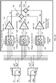
- FIG. 2A is a block diagram of a number of components disposed in a transmit chain 24, in accordance with one exemplary embodiment of the present invention.
- Transmit chain 24 is shown as including, in part, filters 102, 104, quadrature upconverters 120, 122, 124, driver amplifiers 130, 132, 134, and combiners 140, 142.
- Transmit chain 24 is adapted to upconvert the frequency of the signals it receives and suppress spurious harmonics generated in driver amplifiers 130, 132, and 134, as described further below.
- Filter 102 filters out undesired signals from the I-channel baseband signals I bb and IB bb to generate filtered baseband signals I bb_ F and IB bb_ F. Signals I bb and IB bb are inverse (complement) of one another. Likewise, filter 104 filters out undesired signals from Q-channel baseband signals Q bb and QB bb to generate filtered baseband signals Q bb_ F and QB bb_ F.
- quadrature upconverter 120 receives four phases 315, 135, 45, 225 of a local oscillator (not shown).
- Quadrature upconverter 122 receives four phases 0, 180, 90, 270 of the local oscillator.
- Quadrature upconverter 124 receives four phases 45, 225, 135, 315 of the local oscillator.
- the four phases of the LO signal received by quadrature upconverter 120 lead the corresponding phases of the LO signal received by quadrature upconverter 122 by 45°.
- the four phases of the LO signal received by quadrature upconverter 124 lag the corresponding phases of the LO signal received by quadrature upconverter 122 by 45°.
- Quadrature upconverter 120 performs frequency upconversion to generate RF signals I 1 , Q 1 ; quadrature upconverter 122 performs frequency upconversion to generate RF signals I 2 , Q 2 ; and quadrature upconverter 124 performs frequency upconversion to generate RF signals I 3 , Q 3 .
- Amplifier 130 amplifies signals I 1 /Q 1 to generate a pair of complementary signals A and AB; amplifier 132 amplifies signals I 2 /Q 2 to generate a pair of complementary signals B and BB; and amplifier 134 amplifies signals I 3 /Q 3 to generate a pair of complementary signals C and CB.
- FIG. 2B is a generalized block diagram of the transmit chain illustrated in Figure 2A , in accordance with one exemplary embodiment of the present invention.
- the transmit chain 26 may include M filters 202 each receiving one of the M input signals and output one of the output signals out 1 through out M .
- Each output signal (e.g., out 1 ) may include a signal and its inverse.
- the output signals may enter the generalized upconverters 222 1 through 222 N .
- Each of the generalized upconverters 222 may include M/2 double balanced mixers.
- Output of the N upconverters 222 may be amplified with N amplifiers 224 1 through 224 N .
- the amplified signals may then be combined with the generalized combiner 226 to generate output 228.
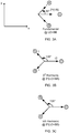
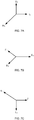
- Figure 3A shows three phasors corresponding to signals A, B and C having a fundamental frequency defined by the local oscillator (LO) frequency of LO and baseband frequency of BB, namely LO+BB.
- LO local oscillator
- Figures 3B and 3C show the same three phasors respectively at the third harmonic frequency of 3*(LO+BB), and fifth harmonic frequency of 5*(LO+BB).
- the sum of the projections (magnitudes) of phasors A and B along the x-axis has to be equal to the magnitude of phasor C along the same axis.
- phasors A and B have a length of 1, because the angle between phasors C and A as well as the angle between phasors C and B is 135°, the x-component of each of phasors A and B has a length (value) of ⁇ 2 2 . Therefore, the sum of the x-components of signals A and B at the third harmonic frequency is equal to ⁇ 2.
- phasor C is selected to have a length that is ⁇ 2 times the lengths of phasors A and B. This causes the three phasors to cancel each other along both the x and y axes.
- amplifier 132 is selected to have a gain that is 2 1 6 times the gains of amplifiers 130, 134. Consequently, if amplifiers 130, 134 have a gain of G, amplifier 132 has a gain of 2 1 6 * G .
- the third harmonic of signals I 2 and Q 2 is amplified by a factor of 2 1 6 3 --which is equal to ⁇ 2.
- the third harmonic of signal C has a magnitude that is greater than that of signals A and B by a factor of 2 1 6 3 which is equal to ⁇ 2.
- the third harmonic of signal CB has a magnitude that is larger than that of signals AB and BB by a factor of ⁇ 2.
- output signal Outp that is generated by combining/adding signals A, B, C has a substantially reduced component at the third harmonic frequency of 3*(LO+BB).
- output signal Outn that is generated by combining/adding signals AB, BB, CB has a substantially reduced component at the third harmonic frequency of 3*(LO+BB).
- amplifier 132 is selected to have a gain that is 2 1 10 times the gains of amplifiers 130, 134. Consequently, if amplifiers 130, 134 have a gain of G, amplifier 132 has a gain of 2 1 10 * G .
- the fifth harmonic of signals I 2 and Q 2 is amplified by a factor of 2 1 10 5 --which is equal to ⁇ 2.
- the fifth harmonic of signal C has a magnitude that is larger than that of signals A and B by a factor of 2 1 10 5 which is equal to ⁇ 2.
- the fifth harmonic of signal CB has a magnitude that is larger than that of signals AB and BB by a factor of ⁇ 2.
- output signal Outp that is generated by combining/adding signals A, B, C has a substantially reduced component at the fifth harmonic frequency of 5*(LO+BB).
- output signal Outn that is generated by combining/adding signals AB, BB, CB has a substantially reduced component at the fifth harmonic frequency of 5*(LO+BB). Consequently, in accordance with the present invention, by adjusting the gain of amplifier 132 relative to the gains of amplifiers 130 and 134, the undesired harmonics caused by non-linearity of the amplifiers is substantially suppressed.
- each of the frequency upconverters 120, 122, 124 may be a composite harmonic-rejective frequency upconverter that, in turn, includes a multitude of upconverters.
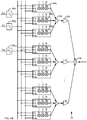
- Figure 4A is a block diagram of another exemplary embodiment of a frequency upconverter.
- Transmit chain 24 of Figure 4A is shown as including, in part, filters 102, 104, quadrature upconverters 120 1 , 120 2 , 120 3 collectively forming upconverter 120, quadrature upconverters 122 1 , 122 2 , 122 3 collectively forming upconverter 122, quadrature upconverters 124 1 , 124 2 , 124 3 collectively forming upconverter 124, driver amplifiers 130, 132, 134, and combiners 202, 204, 206, 208, 210,212, 140, 142.
- Transmit chain 24 of Figure 4A is adapted to upconvert the frequency of the signals it receives and suppress the third harmonic frequency of 3*(LO+BB) or fifth harmonic frequency of 5*(LO+BB), as described above in reference to Figures 2 and 3A-3C .
- Transmit chain 24 of Figure 4A is further adapted to suppress the third order spurious mixing product of 3*LO-BB caused by the upconverters, the fifth order spurious mixing product of 5*LO+BB caused by the upconverters, as well as the undesired counter-IM3 product of LO-3*BB caused by the driver amplifiers.
- FIG. 4A While the embodiment of Figure 4A is described with reference to a frequency upconversion circuit having 3 sets of upconverters 120, 122, 124 each set having 3 upconverters (for a total of 9 upconverters), it is understood that other embodiments may have N sets of upconverters with each set including Q upconverters, where N and Q are positive integers. Furthermore, while the frequency upconversion circuit of Figure 4A is shown as receiving 9 sets of phases of the LO signal with each set including 4 different phases of the LO signal, it is understood that other embodiments may receive N ⁇ Q sets of phases of a LO signal with each set including M different phases of the LO signal, where N, Q and M are positive integers.
- Filter 102 filters out undesired signals from the I-channel baseband signals I bb and IB bb to generate filtered baseband signals I bb_ F and IB bb_ F. Signals I bb and IB bb are inverse of one another. Likewise, filter 104 filters out undesired signals from Q-channel baseband signals Q bb and QB bb to generate filtered baseband signals Q bb_ F and QB bb_ F.
- the four filtered baseband signals I bb_ F, IB bb_ F, Q bb_ F and QB bb_ F that are 90° phase shifted with respect to one another are applied to each of the quadrature upconverters 120 1 , 120 2 , 120 3 , 122 1 , 122 2 , 122 3 , 124 1 , 124 2 , 124 3 .
- upconverter 120 1 receives four phases 270, 90, 0, 180 of the local oscillator; upconverter 120 2 receives four phases 315, 135, 45, 225 of the local oscillator; upconverter 120 3 receives four phases 0, 180, 90, 270, of the local oscillator; upconverter 122 1 receives four phases 315, 135, 45, 225 of the local oscillator; upconverter 122 2 receives four phases 0, 180, 90, 270 of the local oscillator; upconverter 122 3 receives four phases 45, 225, 135, 315 of the local oscillator; upconverter 124 1 receives four phases 0, 180, 90, 270 of the local oscillator; upconverter 124 2 receives four phases 45, 225, 135, 315 of the local oscillator; and upconverter 124 3 receives four phases 90, 270, 180, 0 of the local oscillator (LO).
- LO local oscillator
- the four phases of the LO signal received by upconverter 120 1 lead the corresponding phases of the LO signal received by upconverter 120 2 by 45°, and the four phases of the LO signal received by upconverter 120 3 lag the corresponding phases of the LO signal received by quadrature upconverter 120 2 by 45°.
- the four phases of the LO signal received by upconverter 122 1 lead the corresponding phases of the LO signal received by upconverter 122 2 by 45°
- the four phases of the LO signal received by upconverter 122 3 lag the corresponding phases of the LO signal received by quadrature upconverter 122 2 by 45°.
- the four phases of the LO signal received by upconverter 124 1 lead the corresponding phases of the LO signal received by upconverter 124 2 by 45°, and the four phases of the LO signal received by upconverter 124 3 lag the corresponding phases of the LO signal received by quadrature upconverter 124 2 by 45°.
- the four phases of the LO signal received by upconverter 120 i lead the corresponding phases of the LO signal received by quadrature upconverter 122 i by 45°, where i is an integer varying from 1 to 3 in this exemplary embodiment.
- the four phases 315, 135, 45, 225 of the LO signal received by upconverter 120 2 lead the corresponding four phases 0, 180, 90, 270 of the LO signal received by quadrature upconverter 122 2 by 45°.
- the four phases of the LO signal received by upconverter 124 i lag the corresponding phases of the LO signal received by quadrature upconverter 122 i by 45°.
- the four phases 45, 225, 135, 315 of the LO signal received by upconverter 124 2 lag the corresponding phases 0, 180, 90, 270 of the LO signal received by quadrature upconverter 122 2 by 45°.
- Upconverter 120 1 performs frequency upconversion to generate upconverted in-phase and inverse RF signals G 1 , G 2 ; upconverter 120 2 performs frequency upconversion to generate upconverted in-phase and inverse RF signals H 1 , H 2 ; upconverter 120 3 performs frequency upconversion to generate upconverted in-phase and its inverse RF signals I 1 , I 2 ; upconverter 122 1 performs frequency upconversion to generate upconverted in-phase and inverse RF signals D 1 , D 2 ; upconverter 122 2 performs frequency upconversion to generate upconverted in-phase and inverse RF signals E 1 , E 2 ; upconverter 122 3 performs frequency upconversion to generate upconverted in-phase and inverse RF signals F 1 , F 2 ; upconverter 124 1 performs frequency upconversion to generate upconverted in-phase and inverse RF signals J 1 , J 2 ; upconverter 124 2 performs frequency up
- Combiner 202 is adapted to add/combine signals G 1 , H 1 , I 1 to generate signal M; combiner 204 is adapted to add/combine signals G 2 , H 2 , I 2 to generate signal N; combiner 206 is adapted to add/combine signals D 1 , E 1 , F 1 to generate signal O; combiner 208 is adapted to add/combine signals D 2 , E 2 , F 2 to generate signal p; combiner 210 is adapted to add/combine signals J 1 , K 1 , L 1 to generate signal S; and combiner 212 is adapted to add/combine signals J 2 , K 2 , L 2 to generate signal T.
- Amplifier 130 amplifies signals M and N to generate a pair of complementary signals A and AB; amplifier 132 amplifies signals O and P to generate a pair of complementary signals B and BB; and amplifier 134 amplifies signals S and T to generate a pair of complementary signals C and CB.
- signals G 1 and G 2 respectively lead signals H 1 and H 2 by 45°.
- signals I 1 and I 2 respectively lag signals H 1 and H 2 by 45°.
- signals D 1 and D 2 respectively lead signals E 1 and E 2 by 45°
- signals F 1 and F 2 respectively lag signals E 1 and E 2 by 45°.
- signals J 1 and J 2 respectively lead signals K 1 and K 2 by 45°
- signals L 1 and L 2 respectively lag signals K 1 and K 2 by 45°.
- FIG. 4B is a generalized block diagram of the transmit chain illustrated in Figure 4A , in accordance with one exemplary embodiment of the present invention.
- the transmit chain 28 may include M filters 202 each receiving one of the M input signals and output one of the output signals out 1 through out M .
- Each output signal (e.g., out 1 ) may include a signal and its inverse.
- the output signals may enter each of the N sets of the generalized upconverters (e.g., 440 1 through 440 Q ).
- Each of the generalized upconverters 440 may include M/2 double balanced mixers or M single balanced mixers.
- Output of the Q upconverters 440 may be combined with combiner 450 before being amplified with amplifier 224 1 .
- Outputs of the N amplifiers 224 1 through 224 N may then be combined with the generalized combiner 226 to generate output 228.
- Figure 5A shows three phasors associated with signals I 1 , G 1 and H 1 having a fundamental frequency defined by the local oscillator (LO) frequency of LO and baseband frequency of BB, namely LO+BB.
- LO local oscillator
- FIG. 5A shows three phasors associated with signals E 1 , F 1 and D 1 having a fundamental frequency of LO+BB.
- signal D 1 leads signal E 1 by 45° and signal F 1 lags signal E 1 by 45°.
- Figure 5C shows three phasors associated with signals J 1 , K 1 and L 1 having a fundamental frequency of LO+BB. As seen in Figure 5C , at this fundamental frequency, signal J 1 leads signal K 1 by 45° and signal L 1 lags signal K 1 by 45°.
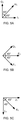
- Figure 6A shows the three phasors associated with signals G 1 , H 1 , I 1 at the spurious upconversion mixing product frequency of (3*LO-BB).
- the value (amplitude) of signal H 1 is selected to be ⁇ 2 times greater than the value of each of signals G 1 and I 1 .
- the y-component of signal H 1 cancels signal G 1
- the x-component of signal H 1 cancels signal I 1 .
- Figure 6B shows the three phasors associated with signals D 1 , E 1 , F 1 at the spurious upconversion mixing product frequency of (3*LO-BB).
- the value of signal E 1 is selected to be ⁇ 2 times greater than the value of each of signals D 1 and F 1 .
- FIG. 7C shows the three phasors associated with signals J 1 , K1, L 1 at the spurious upconversion mixing product frequency of (3*LO-BB).
- the value of signal K 1 is selected to be ⁇ 2 times greater than the value of each of signals L 1 and J 1 .
- the x-component of signal K 1 cancels signal J 1
- the y-component of signals K 1 cancels signal L 1 .
- the spurious upconversion mixing product at frequency (3*LO-BB) is substantially reduced at (i) the outputs M and N of combiners 202, 204, (ii) the outputs O and P of combiners 206, 208; and (iii) the outputs S, T of combiners 201, 212.
- the spurious upconversion mixing products at frequency (3*LO-BB) is canceled or substantially reduced at the outputs of combiners, i.e., at the inputs of amplifiers 130, 132, 134.
- Figure 7A shows the three phasors associated with signals G 1 , H 1 , I 1 at the spurious upconversion product frequency of (5*LO+BB).
- the value of signal H 1 is selected to be ⁇ 2 times greater than the value of each of signals G 1 and H 1 .
- the y-component of signal H 1 cancels signal G 1
- the x-component of signal H 1 cancels signal I 1 .
- Figure 7B shows the three phasors associated with signals D 1 , E 1 , F 1 at the spurious upconversion product frequency of (5*LO+BB).
- the value of signal E 1 is selected to be ⁇ 2 times greater than the value of each of signals D 1 and F 1 .
- the y-components of signals D 1 and F 1 cancel each other.
- the sum of the x-components of signals D 1 and F 1 cancel signal E 1 .
- Figure 7C shows the three phasors associated with signals J 1 , K1, L 1 at the spurious upconversion product frequency of (5*LO+BB).
- the value of signal K 1 is selected to be ⁇ 2 times greater than the value of each of signals L 1 and J 1 .
- the x-component of signal K 1 cancels signal J 1
- the y-component of signals K 1 cancels signal L 1 .
- the spurious upconversion products at frequency (5*LO+BB) is substantially canceled at (i) the outputs M and N of combiners 202, 204, (ii) the outputs O and P of combiners 206, 208; and (iii) the outputs S, T of combiners 201, 212.
- the spurious upconversion product at frequency (5*LO+BB) is canceled or substantially reduced at the outputs of combiners, i.e., at the inputs of the amplifiers.
- the proposed method also rejects undesired components at frequency LO-3BB.
- the undesired components at frequency LO-3BB are generated because of the presence of third order nonlinearity in amplifiers 130,132,134 as a result of intermodulation of input signals with spectral components at LO+BB and 3*LO-BB.
- the embodiment as illustrated in Figure 4A rejects 3*LO-BB components by design at the combiner outputs 202, 204, 206, 208, 210 and 212. As a result of this rejection of the 3*LO-BB component, no substantial LO-3*BB product can be generated at the outputs of amplifiers 130, 132, 134.
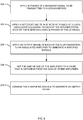
- FIG. 8 is a flowchart 200 for a communication method, in accordance with one embodiment of the present invention.
- M phases of a signal to be transmitted are applied 202 to N upconverters.
- One of N sets of phases of a LO signal are also applied 204 to each of the N upconverters.
- Each of the N sets of phases includes a different one of M phases of the LO signal.
- the output of each upconverter is applied 206 to an associated amplifier to generate N amplified signals.
- the gain of at least one of the amplifiers is set 208 to a value that is different from the gain of the remaining amplifiers.
- the amplified signals are combined 216 to generate an output signal that has a substantially reduced harmonics of the upconverted signal to be transmitted.
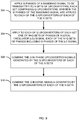
- FIG. 9 is a flowchart 200 for a communication method, in accordance with one embodiment of the present invention.
- M phases of a signal to be transmitted are applied 304 to N sets of upconverters.
- Each of the N sets includes Q upconverters.
- the M phases of the signal are applied to each of the Q upconverters of each of the N sets.
- One of N ⁇ Q sets of phases of a local oscillator signal are also applied 306 to each of the N ⁇ Q upconverters.
- Each of the N ⁇ Q sets includes M phases of the LO signal.
- Each of the Q upconverters generates an upconverted in-phase signal and an upconverted inverse signal in response.
- the Q in-phase signals generated by the Q upconverters of each of the N sets are combined 308 to generate N combined in-phase signals.
- the Q inverse signals generated by the Q upconverters of each of the N sets are also combined 310 to generate N combined inverse signals.
- the above embodiments of the present invention are illustrative and not limitative.
- the embodiments of the present invention are not limited by the number of upconverters, the number of sets of LO phases, or the number of LO phases in each such set.
Landscapes
- Engineering & Computer Science (AREA)
- Power Engineering (AREA)
- Computer Networks & Wireless Communication (AREA)
- Signal Processing (AREA)
- Physics & Mathematics (AREA)
- Nonlinear Science (AREA)
- Transmitters (AREA)
- Amplifiers (AREA)
Applications Claiming Priority (2)
| Application Number | Priority Date | Filing Date | Title |
|---|---|---|---|
| US13/949,736 US8976897B2 (en) | 2013-07-24 | 2013-07-24 | Suppression of spurious harmonics generated in TX driver amplifiers |
| PCT/US2014/047160 WO2015013125A1 (en) | 2013-07-24 | 2014-07-18 | Suppression of spurious harmonics generated in tx driver amplifiers |
Publications (2)
| Publication Number | Publication Date |
|---|---|
| EP3025425A1 EP3025425A1 (en) | 2016-06-01 |
| EP3025425B1 true EP3025425B1 (en) | 2017-08-23 |
Family
ID=51301344
Family Applications (1)
| Application Number | Title | Priority Date | Filing Date |
|---|---|---|---|
| EP14750265.2A Active EP3025425B1 (en) | 2013-07-24 | 2014-07-18 | Suppression of spurious harmonics generated in tx driver amplifiers |
Country Status (6)
| Country | Link |
|---|---|
| US (1) | US8976897B2 (enExample) |
| EP (1) | EP3025425B1 (enExample) |
| JP (1) | JP6416253B2 (enExample) |
| KR (1) | KR20160039212A (enExample) |
| CN (1) | CN105409118B (enExample) |
| WO (1) | WO2015013125A1 (enExample) |
Families Citing this family (13)
| Publication number | Priority date | Publication date | Assignee | Title |
|---|---|---|---|---|
| US9350396B2 (en) * | 2014-03-26 | 2016-05-24 | Marvell World Trade Ltd. | Systems and methods for reducing signal distortion in wireless communication |
| JP2016167781A (ja) * | 2015-03-10 | 2016-09-15 | 富士通株式会社 | 無線通信装置及び無線通信装置の制御方法 |
| US9391651B1 (en) | 2015-04-07 | 2016-07-12 | Qualcomm Incorporated | Amplifier with reduced harmonic distortion |
| US10171034B2 (en) | 2016-04-08 | 2019-01-01 | Mediatek Inc. | Phase-rotated harmonic-rejection mixer apparatus |
| US10419046B2 (en) * | 2016-05-26 | 2019-09-17 | Mediatek Singapore Pte. Ltd | Quadrature transmitter, wireless communication unit, and method for spur suppression |
| US10009050B2 (en) * | 2016-05-26 | 2018-06-26 | Mediatek Singapore Pte. Ltd. | Quadrature transmitter, wireless communication unit, and method for spur suppression |
| US10338646B1 (en) | 2018-02-22 | 2019-07-02 | Lg Electronics Inc. | Radio frequency amplifier circuit and mobile terminal having the same |
| KR102040546B1 (ko) * | 2018-02-22 | 2019-11-06 | 엘지전자 주식회사 | 무선 주파수 증폭기 회로 및 이를 구비하는 이동 단말기 |
| WO2019237260A1 (zh) * | 2018-06-12 | 2019-12-19 | 华为技术有限公司 | 一种发射机、本振校准电路及校准方法 |
| KR102735221B1 (ko) | 2020-05-25 | 2024-11-27 | 삼성전자주식회사 | 디지털 rf 송신기 및 이를 포함하는 무선 통신 장치 |
| WO2021091619A1 (en) * | 2020-05-30 | 2021-05-14 | Futurewei Technologies, Inc. | 6-phase digitally assisted harmonic rejection transceiver using rf interpolation |
| CN115720699B (zh) * | 2020-05-30 | 2026-01-30 | 华为技术有限公司 | 具有占空比控制的谐波抑制收发器 |
| CN115769488B (zh) * | 2020-05-30 | 2025-05-02 | 华为技术有限公司 | 双三相谐波抑制收发器 |
Family Cites Families (20)
| Publication number | Priority date | Publication date | Assignee | Title |
|---|---|---|---|---|
| GB2325102B (en) * | 1997-05-09 | 2001-10-10 | Nokia Mobile Phones Ltd | Down conversion mixer |
| US6799020B1 (en) * | 1999-07-20 | 2004-09-28 | Qualcomm Incorporated | Parallel amplifier architecture using digital phase control techniques |
| US7130604B1 (en) | 2002-06-06 | 2006-10-31 | National Semiconductor Corporation | Harmonic rejection mixer and method of operation |
| US7409010B2 (en) * | 2003-06-10 | 2008-08-05 | Shared Spectrum Company | Method and system for transmitting signals with reduced spurious emissions |
| DE602005015942D1 (enExample) | 2004-03-12 | 2009-09-24 | R F Magic Inc | |
| EP1820277B1 (en) | 2004-12-10 | 2010-02-03 | Maxlinear, Inc. | Harmonic reject receiver architecture and mixer |
| US20090143031A1 (en) | 2005-03-11 | 2009-06-04 | Peter Shah | Harmonic suppression mixer and tuner |
| US7509110B2 (en) | 2005-03-14 | 2009-03-24 | Broadcom Corporation | High-order harmonic rejection mixer using multiple LO phases |
| GB2427090B (en) * | 2005-06-08 | 2011-01-12 | Zarlink Semiconductor Ltd | Method of reducing imbalance in a quadrature frequency converter, method of measuring imbalance in such a converter, and apparatus for performing such method |
| US20070230615A1 (en) * | 2006-03-31 | 2007-10-04 | Taylor Stewart S | Reduced distortion amplifier |
| US8599938B2 (en) * | 2007-09-14 | 2013-12-03 | Qualcomm Incorporated | Linear and polar dual mode transmitter circuit |
| US8509346B2 (en) * | 2007-10-10 | 2013-08-13 | St-Ericsson Sa | Transmitter with reduced power consumption and increased linearity and dynamic range |
| KR101433845B1 (ko) * | 2008-01-23 | 2014-08-27 | 삼성전자주식회사 | 다중 안테나 무선통신 시스템에서 피드백 경로를 공유하는디지털 선 왜곡 장치 및 방법 |
| US8165538B2 (en) | 2008-06-25 | 2012-04-24 | Skyworks Solutions, Inc. | Systems and methods for implementing a harmonic rejection mixer |
| US8515371B2 (en) | 2008-10-31 | 2013-08-20 | Synopsys, Inc. | Programmable IF output receiver, and applications thereof |
| US8358680B2 (en) * | 2008-12-23 | 2013-01-22 | Apple Inc. | Reducing power levels associated with two or more signals using peak reduction distortion that is derived from a combined signal |
| WO2010089700A1 (en) | 2009-02-04 | 2010-08-12 | Nxp B.V. | Polyphase harmonic rejection mixer |
| JP5670417B2 (ja) * | 2009-03-17 | 2015-02-18 | スカイワークス ソリューションズ, インコーポレイテッドSkyworks Solutions, Inc. | Sawレス、lnaレス低ノイズ受信器 |
| WO2012014307A1 (ja) | 2010-07-29 | 2012-02-02 | 富士通株式会社 | 信号生成回路及びそれを有する無線送受信装置 |
| US8542769B2 (en) * | 2011-06-09 | 2013-09-24 | St-Ericsson Sa | High output power digital TX |
-
2013
- 2013-07-24 US US13/949,736 patent/US8976897B2/en active Active
-
2014
- 2014-07-18 KR KR1020167003979A patent/KR20160039212A/ko not_active Withdrawn
- 2014-07-18 JP JP2016529795A patent/JP6416253B2/ja not_active Expired - Fee Related
- 2014-07-18 CN CN201480041190.XA patent/CN105409118B/zh active Active
- 2014-07-18 EP EP14750265.2A patent/EP3025425B1/en active Active
- 2014-07-18 WO PCT/US2014/047160 patent/WO2015013125A1/en not_active Ceased
Non-Patent Citations (1)
| Title |
|---|
| None * |
Also Published As
| Publication number | Publication date |
|---|---|
| US20150030105A1 (en) | 2015-01-29 |
| WO2015013125A1 (en) | 2015-01-29 |
| KR20160039212A (ko) | 2016-04-08 |
| CN105409118A (zh) | 2016-03-16 |
| CN105409118B (zh) | 2018-08-10 |
| JP2016530794A (ja) | 2016-09-29 |
| US8976897B2 (en) | 2015-03-10 |
| EP3025425A1 (en) | 2016-06-01 |
| JP6416253B2 (ja) | 2018-10-31 |
Similar Documents
| Publication | Publication Date | Title |
|---|---|---|
| EP3025425B1 (en) | Suppression of spurious harmonics generated in tx driver amplifiers | |
| US8391809B1 (en) | System and method for multi-band predistortion | |
| EP3213409B1 (en) | Phase shifting mixer | |
| US9432063B2 (en) | Radio frequency signal transceiving and processing method, device, and base station system | |
| EP3108630B1 (en) | Quadrature combining and adjusting | |
| US10033338B2 (en) | Switched inductor/transformer for dual-band low-noise amplifier (LNA) | |
| US10666285B1 (en) | Digital-to-analog converter (DAC) with mixing-mode parallel path image attenuation | |
| US20120280840A1 (en) | Multiple-mode broadband wireless communication device and method | |
| US20140274199A1 (en) | Noise Cancellation Apparatus and Method | |
| US10673411B2 (en) | Large-signal GM3 cancellation technique for highly-linear active mixers | |
| WO2024196562A1 (en) | Crest factor reduction for adjusting digital-to- analog converter output power | |
| EP3491736B1 (en) | Amplification systems | |
| CN115769489B (zh) | 使用rf插值的6相数字辅助谐波抑制收发器 | |
| US12592729B2 (en) | Hybrid distortion suppression system and method | |
| WO2025064414A1 (en) | Feedback receiver (fbrx) path and closed loop control for transmitter (tx) interference cancellation | |
| CN109314536A (zh) | 偏置无源混频器 | |
| US20250350305A1 (en) | Split main and predistortion signal paths with separate digital-to-analog converters for supporting digital predistortion in transmitters | |
| US20240339994A1 (en) | Systems and techniques for magnetic field cancellation for a radio architecture | |
| US11063617B1 (en) | Bandtilt correction using combined signal and image passive mixers | |
| US20250300605A1 (en) | Transimpedance amplifier with virtual ground shunt resistor | |
| US20230097399A1 (en) | High linearity modes in wireless receivers | |
| US20160079985A1 (en) | Quadrature local oscillator phase synthesis and architecture for divide-by-odd-number frequency dividers | |
| CN114826287A (zh) | 一种天线信号处理装置 |
Legal Events
| Date | Code | Title | Description |
|---|---|---|---|
| PUAI | Public reference made under article 153(3) epc to a published international application that has entered the european phase |
Free format text: ORIGINAL CODE: 0009012 |
|
| 17P | Request for examination filed |
Effective date: 20160223 |
|
| AK | Designated contracting states |
Kind code of ref document: A1 Designated state(s): AL AT BE BG CH CY CZ DE DK EE ES FI FR GB GR HR HU IE IS IT LI LT LU LV MC MK MT NL NO PL PT RO RS SE SI SK SM TR |
|
| AX | Request for extension of the european patent |
Extension state: BA ME |
|
| 17Q | First examination report despatched |
Effective date: 20160728 |
|
| DAX | Request for extension of the european patent (deleted) | ||
| REG | Reference to a national code |
Ref country code: DE Ref legal event code: R079 Ref document number: 602014013555 Country of ref document: DE Free format text: PREVIOUS MAIN CLASS: H03F0001320000 Ipc: H03D0007160000 |
|
| GRAP | Despatch of communication of intention to grant a patent |
Free format text: ORIGINAL CODE: EPIDOSNIGR1 |
|
| RIC1 | Information provided on ipc code assigned before grant |
Ipc: H03F 3/189 20060101ALI20170210BHEP Ipc: H04B 1/04 20060101ALI20170210BHEP Ipc: H03F 3/24 20060101ALI20170210BHEP Ipc: H03F 3/60 20060101ALI20170210BHEP Ipc: H03D 7/16 20060101AFI20170210BHEP Ipc: H03F 1/32 20060101ALI20170210BHEP |
|
| INTG | Intention to grant announced |
Effective date: 20170308 |
|
| GRAS | Grant fee paid |
Free format text: ORIGINAL CODE: EPIDOSNIGR3 |
|
| GRAA | (expected) grant |
Free format text: ORIGINAL CODE: 0009210 |
|
| AK | Designated contracting states |
Kind code of ref document: B1 Designated state(s): AL AT BE BG CH CY CZ DE DK EE ES FI FR GB GR HR HU IE IS IT LI LT LU LV MC MK MT NL NO PL PT RO RS SE SI SK SM TR |
|
| REG | Reference to a national code |
Ref country code: GB Ref legal event code: FG4D |
|
| REG | Reference to a national code |
Ref country code: CH Ref legal event code: EP |
|
| REG | Reference to a national code |
Ref country code: AT Ref legal event code: REF Ref document number: 922321 Country of ref document: AT Kind code of ref document: T Effective date: 20170915 |
|
| REG | Reference to a national code |
Ref country code: IE Ref legal event code: FG4D |
|
| REG | Reference to a national code |
Ref country code: DE Ref legal event code: R096 Ref document number: 602014013555 Country of ref document: DE |
|
| REG | Reference to a national code |
Ref country code: NL Ref legal event code: MP Effective date: 20170823 |
|
| REG | Reference to a national code |
Ref country code: LT Ref legal event code: MG4D |
|
| REG | Reference to a national code |
Ref country code: AT Ref legal event code: MK05 Ref document number: 922321 Country of ref document: AT Kind code of ref document: T Effective date: 20170823 |
|
| PG25 | Lapsed in a contracting state [announced via postgrant information from national office to epo] |
Ref country code: NL Free format text: LAPSE BECAUSE OF FAILURE TO SUBMIT A TRANSLATION OF THE DESCRIPTION OR TO PAY THE FEE WITHIN THE PRESCRIBED TIME-LIMIT Effective date: 20170823 Ref country code: SE Free format text: LAPSE BECAUSE OF FAILURE TO SUBMIT A TRANSLATION OF THE DESCRIPTION OR TO PAY THE FEE WITHIN THE PRESCRIBED TIME-LIMIT Effective date: 20170823 Ref country code: NO Free format text: LAPSE BECAUSE OF FAILURE TO SUBMIT A TRANSLATION OF THE DESCRIPTION OR TO PAY THE FEE WITHIN THE PRESCRIBED TIME-LIMIT Effective date: 20171123 Ref country code: HR Free format text: LAPSE BECAUSE OF FAILURE TO SUBMIT A TRANSLATION OF THE DESCRIPTION OR TO PAY THE FEE WITHIN THE PRESCRIBED TIME-LIMIT Effective date: 20170823 Ref country code: AT Free format text: LAPSE BECAUSE OF FAILURE TO SUBMIT A TRANSLATION OF THE DESCRIPTION OR TO PAY THE FEE WITHIN THE PRESCRIBED TIME-LIMIT Effective date: 20170823 Ref country code: FI Free format text: LAPSE BECAUSE OF FAILURE TO SUBMIT A TRANSLATION OF THE DESCRIPTION OR TO PAY THE FEE WITHIN THE PRESCRIBED TIME-LIMIT Effective date: 20170823 Ref country code: LT Free format text: LAPSE BECAUSE OF FAILURE TO SUBMIT A TRANSLATION OF THE DESCRIPTION OR TO PAY THE FEE WITHIN THE PRESCRIBED TIME-LIMIT Effective date: 20170823 |
|
| PG25 | Lapsed in a contracting state [announced via postgrant information from national office to epo] |
Ref country code: ES Free format text: LAPSE BECAUSE OF FAILURE TO SUBMIT A TRANSLATION OF THE DESCRIPTION OR TO PAY THE FEE WITHIN THE PRESCRIBED TIME-LIMIT Effective date: 20170823 Ref country code: PL Free format text: LAPSE BECAUSE OF FAILURE TO SUBMIT A TRANSLATION OF THE DESCRIPTION OR TO PAY THE FEE WITHIN THE PRESCRIBED TIME-LIMIT Effective date: 20170823 Ref country code: RS Free format text: LAPSE BECAUSE OF FAILURE TO SUBMIT A TRANSLATION OF THE DESCRIPTION OR TO PAY THE FEE WITHIN THE PRESCRIBED TIME-LIMIT Effective date: 20170823 Ref country code: LV Free format text: LAPSE BECAUSE OF FAILURE TO SUBMIT A TRANSLATION OF THE DESCRIPTION OR TO PAY THE FEE WITHIN THE PRESCRIBED TIME-LIMIT Effective date: 20170823 Ref country code: GR Free format text: LAPSE BECAUSE OF FAILURE TO SUBMIT A TRANSLATION OF THE DESCRIPTION OR TO PAY THE FEE WITHIN THE PRESCRIBED TIME-LIMIT Effective date: 20171124 Ref country code: BG Free format text: LAPSE BECAUSE OF FAILURE TO SUBMIT A TRANSLATION OF THE DESCRIPTION OR TO PAY THE FEE WITHIN THE PRESCRIBED TIME-LIMIT Effective date: 20171123 Ref country code: IS Free format text: LAPSE BECAUSE OF FAILURE TO SUBMIT A TRANSLATION OF THE DESCRIPTION OR TO PAY THE FEE WITHIN THE PRESCRIBED TIME-LIMIT Effective date: 20171223 |
|
| PG25 | Lapsed in a contracting state [announced via postgrant information from national office to epo] |
Ref country code: DK Free format text: LAPSE BECAUSE OF FAILURE TO SUBMIT A TRANSLATION OF THE DESCRIPTION OR TO PAY THE FEE WITHIN THE PRESCRIBED TIME-LIMIT Effective date: 20170823 Ref country code: CZ Free format text: LAPSE BECAUSE OF FAILURE TO SUBMIT A TRANSLATION OF THE DESCRIPTION OR TO PAY THE FEE WITHIN THE PRESCRIBED TIME-LIMIT Effective date: 20170823 Ref country code: RO Free format text: LAPSE BECAUSE OF FAILURE TO SUBMIT A TRANSLATION OF THE DESCRIPTION OR TO PAY THE FEE WITHIN THE PRESCRIBED TIME-LIMIT Effective date: 20170823 |
|
| REG | Reference to a national code |
Ref country code: DE Ref legal event code: R097 Ref document number: 602014013555 Country of ref document: DE |
|
| PG25 | Lapsed in a contracting state [announced via postgrant information from national office to epo] |
Ref country code: SM Free format text: LAPSE BECAUSE OF FAILURE TO SUBMIT A TRANSLATION OF THE DESCRIPTION OR TO PAY THE FEE WITHIN THE PRESCRIBED TIME-LIMIT Effective date: 20170823 Ref country code: IT Free format text: LAPSE BECAUSE OF FAILURE TO SUBMIT A TRANSLATION OF THE DESCRIPTION OR TO PAY THE FEE WITHIN THE PRESCRIBED TIME-LIMIT Effective date: 20170823 Ref country code: SK Free format text: LAPSE BECAUSE OF FAILURE TO SUBMIT A TRANSLATION OF THE DESCRIPTION OR TO PAY THE FEE WITHIN THE PRESCRIBED TIME-LIMIT Effective date: 20170823 Ref country code: EE Free format text: LAPSE BECAUSE OF FAILURE TO SUBMIT A TRANSLATION OF THE DESCRIPTION OR TO PAY THE FEE WITHIN THE PRESCRIBED TIME-LIMIT Effective date: 20170823 |
|
| REG | Reference to a national code |
Ref country code: FR Ref legal event code: PLFP Year of fee payment: 5 |
|
| PLBE | No opposition filed within time limit |
Free format text: ORIGINAL CODE: 0009261 |
|
| STAA | Information on the status of an ep patent application or granted ep patent |
Free format text: STATUS: NO OPPOSITION FILED WITHIN TIME LIMIT |
|
| 26N | No opposition filed |
Effective date: 20180524 |
|
| PG25 | Lapsed in a contracting state [announced via postgrant information from national office to epo] |
Ref country code: SI Free format text: LAPSE BECAUSE OF FAILURE TO SUBMIT A TRANSLATION OF THE DESCRIPTION OR TO PAY THE FEE WITHIN THE PRESCRIBED TIME-LIMIT Effective date: 20170823 |
|
| REG | Reference to a national code |
Ref country code: CH Ref legal event code: PL |
|
| PG25 | Lapsed in a contracting state [announced via postgrant information from national office to epo] |
Ref country code: MC Free format text: LAPSE BECAUSE OF FAILURE TO SUBMIT A TRANSLATION OF THE DESCRIPTION OR TO PAY THE FEE WITHIN THE PRESCRIBED TIME-LIMIT Effective date: 20170823 Ref country code: LU Free format text: LAPSE BECAUSE OF NON-PAYMENT OF DUE FEES Effective date: 20180718 |
|
| REG | Reference to a national code |
Ref country code: BE Ref legal event code: MM Effective date: 20180731 |
|
| REG | Reference to a national code |
Ref country code: IE Ref legal event code: MM4A |
|
| PG25 | Lapsed in a contracting state [announced via postgrant information from national office to epo] |
Ref country code: CH Free format text: LAPSE BECAUSE OF NON-PAYMENT OF DUE FEES Effective date: 20180731 Ref country code: IE Free format text: LAPSE BECAUSE OF NON-PAYMENT OF DUE FEES Effective date: 20180718 Ref country code: LI Free format text: LAPSE BECAUSE OF NON-PAYMENT OF DUE FEES Effective date: 20180731 |
|
| PG25 | Lapsed in a contracting state [announced via postgrant information from national office to epo] |
Ref country code: BE Free format text: LAPSE BECAUSE OF NON-PAYMENT OF DUE FEES Effective date: 20180731 |
|
| PG25 | Lapsed in a contracting state [announced via postgrant information from national office to epo] |
Ref country code: MT Free format text: LAPSE BECAUSE OF NON-PAYMENT OF DUE FEES Effective date: 20180718 |
|
| PG25 | Lapsed in a contracting state [announced via postgrant information from national office to epo] |
Ref country code: TR Free format text: LAPSE BECAUSE OF FAILURE TO SUBMIT A TRANSLATION OF THE DESCRIPTION OR TO PAY THE FEE WITHIN THE PRESCRIBED TIME-LIMIT Effective date: 20170823 |
|
| PG25 | Lapsed in a contracting state [announced via postgrant information from national office to epo] |
Ref country code: PT Free format text: LAPSE BECAUSE OF FAILURE TO SUBMIT A TRANSLATION OF THE DESCRIPTION OR TO PAY THE FEE WITHIN THE PRESCRIBED TIME-LIMIT Effective date: 20170823 |
|
| PG25 | Lapsed in a contracting state [announced via postgrant information from national office to epo] |
Ref country code: HU Free format text: LAPSE BECAUSE OF FAILURE TO SUBMIT A TRANSLATION OF THE DESCRIPTION OR TO PAY THE FEE WITHIN THE PRESCRIBED TIME-LIMIT; INVALID AB INITIO Effective date: 20140718 Ref country code: CY Free format text: LAPSE BECAUSE OF FAILURE TO SUBMIT A TRANSLATION OF THE DESCRIPTION OR TO PAY THE FEE WITHIN THE PRESCRIBED TIME-LIMIT Effective date: 20170823 Ref country code: MK Free format text: LAPSE BECAUSE OF NON-PAYMENT OF DUE FEES Effective date: 20170823 |
|
| PG25 | Lapsed in a contracting state [announced via postgrant information from national office to epo] |
Ref country code: AL Free format text: LAPSE BECAUSE OF FAILURE TO SUBMIT A TRANSLATION OF THE DESCRIPTION OR TO PAY THE FEE WITHIN THE PRESCRIBED TIME-LIMIT Effective date: 20170823 |
|
| PGFP | Annual fee paid to national office [announced via postgrant information from national office to epo] |
Ref country code: GB Payment date: 20240613 Year of fee payment: 11 |
|
| PGFP | Annual fee paid to national office [announced via postgrant information from national office to epo] |
Ref country code: FR Payment date: 20240613 Year of fee payment: 11 |
|
| PGFP | Annual fee paid to national office [announced via postgrant information from national office to epo] |
Ref country code: DE Payment date: 20250616 Year of fee payment: 12 |
|
| GBPC | Gb: european patent ceased through non-payment of renewal fee |
Effective date: 20250718 |
|
| PG25 | Lapsed in a contracting state [announced via postgrant information from national office to epo] |
Ref country code: GB Free format text: LAPSE BECAUSE OF NON-PAYMENT OF DUE FEES Effective date: 20250718 |
|
| PG25 | Lapsed in a contracting state [announced via postgrant information from national office to epo] |
Ref country code: FR Free format text: LAPSE BECAUSE OF NON-PAYMENT OF DUE FEES Effective date: 20250731 |