EP3024034A1 - Semiconductor device - Google Patents
Semiconductor device Download PDFInfo
- Publication number
- EP3024034A1 EP3024034A1 EP14198214.0A EP14198214A EP3024034A1 EP 3024034 A1 EP3024034 A1 EP 3024034A1 EP 14198214 A EP14198214 A EP 14198214A EP 3024034 A1 EP3024034 A1 EP 3024034A1
- Authority
- EP
- European Patent Office
- Prior art keywords
- type
- doped region
- well
- semiconductor device
- doped
- Prior art date
- Legal status (The legal status is an assumption and is not a legal conclusion. Google has not performed a legal analysis and makes no representation as to the accuracy of the status listed.)
- Granted
Links
Images




Classifications
-
- H—ELECTRICITY
- H10—SEMICONDUCTOR DEVICES; ELECTRIC SOLID-STATE DEVICES NOT OTHERWISE PROVIDED FOR
- H10D—INORGANIC ELECTRIC SEMICONDUCTOR DEVICES
- H10D62/00—Semiconductor bodies, or regions thereof, of devices having potential barriers
- H10D62/10—Shapes, relative sizes or dispositions of the regions of the semiconductor bodies; Shapes of the semiconductor bodies
-
- H—ELECTRICITY
- H10—SEMICONDUCTOR DEVICES; ELECTRIC SOLID-STATE DEVICES NOT OTHERWISE PROVIDED FOR
- H10W—GENERIC PACKAGES, INTERCONNECTIONS, CONNECTORS OR OTHER CONSTRUCTIONAL DETAILS OF DEVICES COVERED BY CLASS H10
- H10W10/00—Isolation regions in semiconductor bodies between components of integrated devices
- H10W10/01—Manufacture or treatment
- H10W10/031—Manufacture or treatment of isolation regions comprising PN junctions
-
- H—ELECTRICITY
- H10—SEMICONDUCTOR DEVICES; ELECTRIC SOLID-STATE DEVICES NOT OTHERWISE PROVIDED FOR
- H10D—INORGANIC ELECTRIC SEMICONDUCTOR DEVICES
- H10D18/00—Thyristors
- H10D18/251—Lateral thyristors
-
- H—ELECTRICITY
- H10—SEMICONDUCTOR DEVICES; ELECTRIC SOLID-STATE DEVICES NOT OTHERWISE PROVIDED FOR
- H10D—INORGANIC ELECTRIC SEMICONDUCTOR DEVICES
- H10D62/00—Semiconductor bodies, or regions thereof, of devices having potential barriers
- H10D62/10—Shapes, relative sizes or dispositions of the regions of the semiconductor bodies; Shapes of the semiconductor bodies
- H10D62/117—Shapes of semiconductor bodies
-
- H—ELECTRICITY
- H10—SEMICONDUCTOR DEVICES; ELECTRIC SOLID-STATE DEVICES NOT OTHERWISE PROVIDED FOR
- H10D—INORGANIC ELECTRIC SEMICONDUCTOR DEVICES
- H10D62/00—Semiconductor bodies, or regions thereof, of devices having potential barriers
- H10D62/10—Shapes, relative sizes or dispositions of the regions of the semiconductor bodies; Shapes of the semiconductor bodies
- H10D62/124—Shapes, relative sizes or dispositions of the regions of semiconductor bodies or of junctions between the regions
- H10D62/125—Shapes of junctions between the regions
-
- H—ELECTRICITY
- H10—SEMICONDUCTOR DEVICES; ELECTRIC SOLID-STATE DEVICES NOT OTHERWISE PROVIDED FOR
- H10D—INORGANIC ELECTRIC SEMICONDUCTOR DEVICES
- H10D62/00—Semiconductor bodies, or regions thereof, of devices having potential barriers
- H10D62/60—Impurity distributions or concentrations
-
- H—ELECTRICITY
- H10—SEMICONDUCTOR DEVICES; ELECTRIC SOLID-STATE DEVICES NOT OTHERWISE PROVIDED FOR
- H10D—INORGANIC ELECTRIC SEMICONDUCTOR DEVICES
- H10D64/00—Electrodes of devices having potential barriers
- H10D64/60—Electrodes characterised by their materials
- H10D64/62—Electrodes ohmically coupled to a semiconductor
-
- H—ELECTRICITY
- H10—SEMICONDUCTOR DEVICES; ELECTRIC SOLID-STATE DEVICES NOT OTHERWISE PROVIDED FOR
- H10D—INORGANIC ELECTRIC SEMICONDUCTOR DEVICES
- H10D89/00—Aspects of integrated devices not covered by groups H10D84/00 - H10D88/00
- H10D89/60—Integrated devices comprising arrangements for electrical or thermal protection, e.g. protection circuits against electrostatic discharge [ESD]
- H10D89/601—Integrated devices comprising arrangements for electrical or thermal protection, e.g. protection circuits against electrostatic discharge [ESD] for devices having insulated gate electrodes, e.g. for IGFETs or IGBTs
- H10D89/711—Integrated devices comprising arrangements for electrical or thermal protection, e.g. protection circuits against electrostatic discharge [ESD] for devices having insulated gate electrodes, e.g. for IGFETs or IGBTs using bipolar transistors as protective elements
- H10D89/713—Integrated devices comprising arrangements for electrical or thermal protection, e.g. protection circuits against electrostatic discharge [ESD] for devices having insulated gate electrodes, e.g. for IGFETs or IGBTs using bipolar transistors as protective elements including a PNP transistor and a NPN transistor, wherein each of said transistors has its base region coupled to the collector region of the other transistor, e.g. silicon controlled rectifier [SCR] devices
-
- H—ELECTRICITY
- H10—SEMICONDUCTOR DEVICES; ELECTRIC SOLID-STATE DEVICES NOT OTHERWISE PROVIDED FOR
- H10W—GENERIC PACKAGES, INTERCONNECTIONS, CONNECTORS OR OTHER CONSTRUCTIONAL DETAILS OF DEVICES COVERED BY CLASS H10
- H10W10/00—Isolation regions in semiconductor bodies between components of integrated devices
- H10W10/30—Isolation regions comprising PN junctions
Definitions
- FIG.1 is a semiconductor device 100 with a STI 101 for related art.
- a STI 101 is provided between a P doped region 103 and an N doped region 105. Therefore, a current path CP for transmitting currents from the P doped region 103 to the N doped region 105 must by-pass the STI 101 since materials of the STI 101 are not conductive. In such case, the current path CP is longer, such that the charge/discharge time for the semiconductor device is correspondingly extended, which may causes some disadvantages. For example, if the semiconductor device 100 is applied as an ESD device, the circuit protected by such device is easily broken since the semiconductor device 100 has a low discharge speed.
- one objective of the present application is to provide a semiconductor device that can provide higher discharging speed.
- a semiconductor device comprising a substrate.
- the substrate comprises: a well of type one; a first doped region of type two, provided in the well of type one; a well of type two, adjacent to the well of type one; and a first doped region of type one, doped in the well of type two.
- the substrate comprises no isolating material provided in a current path formed by the first doped region of type two, the well of type one, the well of type two and the first doped region of type one.
- the first type is N type and the second type is P type. In other embodiments, the first type is P type and the second type is N type.
- FIG.1 is a semiconductor device with a STI for related art.
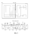
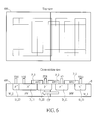
- FIG.2 to FIG.7 are top views and cross-sectional views for semiconductor devices, without silicide, according to embodiments of the present application.
- FIG.8 to FIG.10 are cross-sectional views for semiconductor devices, with silicide, according to embodiments of the present application.
- FIG.11 is a circuit diagram illustrating a voltage providing circuit for providing voltages to the semiconductor devices disclosed in the present application, according to one embodiment of the present application.
- FIG.2 to FIG.7 are top views and cross-sectional views for semiconductor devices according to embodiments of the present application.
- a first type and a second type are applied to respectively indicate the N type or the P type.
- the first type and the second type indicate different meanings in different embodiments.
- the first type indicates the N type
- the second type indicates the P type.
- the first type indicates the P type
- the second type indicates the N type.
- the following embodiment can be implemented by a SCR (Silicon Controlled Rectifier, but not limited.
- the semiconductor device 200 comprises a substrate S.
- the substrate S comprises: a well of type one W_1; a first doped region of type two D_21, provided in the well of type one W_1; a well of type two W_2, adjacent to the well of type one W_1; and a first doped region of type one D_11, doped in the well of type two W_2.
- the substrate S comprises no isolating material, such as above-mentioned STI, provided in a current path CP formed by the first doped region of type two D_21, the well of type one W_1, the well of type two W_2 and the first doped region of type one D_11.
- the current path CP is from 10 to the VSS provided to the first doped region of type one D_11.
- the semiconductor device 200 further comprises a first conductive material CM_1 and a second conductive CM_2 (ex. poly silicide).
- the first conductive material CM_1 is provided on the well of type one W_1 and the well of type two W_2 but not on the first doped region of type one D_11 and the first doped region of type two D_21.
- the second conductive layer CM_2 is provided on the well of type two W_2 but not on the first doped region of type one D_11.
- the first conductive material CM_1 and the second conductive CM_2 can receive different voltages TP, TN to assist the transmission of currents.
- the semiconductor device 200 can comprise a second doped region of type one D_12 provided in the well of type two; and a second doped region of type two D_22 provided in the well of type two W_1.
- the second doped region of type one D_12 and the second doped region of type two D_22 can assist the transmitting of currents.
- the second doped region of type two D_22 and the second doped region of type one D_12 are provided between the first doped region of type one D_11 and the first doped region of type two D_21.
- the first conductive material CM_1 is provided on a region between the first doped region of type two D_21 and the second doped region of type two D_22.
- the second conductive material CM_2 is provided on a region between the first doped region of type one D_11 and the second doped region of type one D_12.
- a protecting material P_1 can be provided as shown in FIG.2 .
- the silicide is not generated at the location of the protecting material P_1.
- FIG.8(a) illustrates an embodiments that the structure in FIG.2 further comprises silicide SI.
- the silicide SI is not generated at the location of the protecting material P_1 shown in FIG.2 .
- the silicide SI is not provided on at least part of the well of type one W_1 adjacent to the first doped region of type two D_21, and at least part of the first doped region of type two D_21 adjacent to the well of type one W_1.
- the semiconductor device 200 in FIG.2 can further comprise: a third doped region of type one D_13, doped in the well of type one W_1, not touching the first doped region of type two D_21; and a third doped region of type two D_23, doped in the well of type two W_2, touching the first doped region of type one D_11.
- the protecting material P_1 covers part of the third doped region of type one D_13. Therefore, in FIG.8(a) , no silicide is provided on at least part of the well of type one W_1 adjacent to the third doped region of type one D_13, and at least part of the third doped region of type one D_13 adjacent to the well of type one W_1.
- the third doped region of type one D_13 is coupled to an operational voltage VDD and the third doped region of type two D_23 is coupled to another operational voltage VSS in this embodiment.
- the semiconductor device 300 comprises similar structure for which of the semiconductor device 200.
- One of the differences is the first type is changed from the N type to the P type, and the second type is changed from the P type to the N type in FIG.3 .
- the operational voltages VDD, VSS are swapped.
- current path CP is inversed, thus it is from the VDD provided to the first doped region of type one D_11 to IO.
- the voltages TP, TN are swapped.
- FIG. 8 (b) illustrates the situation that the semiconductor device 300 comprises silicide SI.
- Other structures and operations for the semiconductor device 300 can be clearly understood based on the description for FIG.2 , thus it is omitted for brevity here.
- the substrate S in the semiconductor device 400 in FIG.4 also comprises the well of type one W_1, the first doped region of type two D_21, the well of type two W_2, the first doped region of type one D_11, the third doped region of type one D_31 and the second doped region of type one D_32.
- the semiconductor device 400 comprises only the second doped region of type two D_22 rather than the first conductive material CM_1, the second conductive material CM_2, the second doped region of type one D_21 and the second doped region of type two D_22 in FIG.2 .
- the second doped region of type two D_22 does not touch the first doped region of type one D_11 and the first doped region of type two D_21.
- the second doped region of type two D_22 in FIG. 4 receives a voltage PTR to assist transmitting the current.
- the semiconductor device 400 also comprises protecting material P_1. Besides, the semiconductor device 400 further comprises the protecting material P_2 and the protecting material P_3.
- the protecting material P_2 is provided on at least part of the first doped region of type two D_21, at least part of the second doped region of type two D_22, and at least part of the well of type one W_1 between the first doped region of type two D_21 and the second doped region of type two D_22.
- the protecting material P_3 is provided on at least part of the first doped region of type one D_11, at least part of the second doped region of type two D_22, and at least part of the well of type two between the first doped region of type one D_11 and the second doped region of type two D_22. Therefore, the silicide SI is not provided at the locations for the protecting materials P_1, P_2 and P_3, as shown in FIG.9(a) .
- the semiconductor device 500 in FIG.5 comprises similar structure for which of the semiconductor device 400.
- One of the differences is the first type is changed from the N type to the P type, and the second type is changed from the P type to the N type in FIG.5 .
- the operational voltages VDD, VSS are swapped.
- current path CP is inversed, thus it is from the VDD provided to the first doped region of type one D_11 to IO.
- FIG.9(b) illustrates the situation that the semiconductor device 500 comprises silicide SI.
- Other structures and operations for the semiconductor device 500 can be clearly understood based on the description for FIG.4 , thus it is omitted for brevity here.
- FIG.6 is a schematic diagram illustrating a semiconductor device 600 according to another embodiment of the present application.
- the second doped region of type two D_22 does not touch the first doped region of type one D_11 in FIG. 4 , but the second doped region of type two D_22 touches (or overlaps) the first doped region of type one D_11 in FIG.6 . Therefore, the protecting material P_3 in FIG.6 is provided on at least part of the first doped region of type one D_11, and at least part of the second doped region of type two D_22.
- the silicide SI is not provided at the locations for the protecting materials P_1, P_2 and P_3 of FIG.6 , as shown in FIG.10(a) .
- the semiconductor device 700 in FIG.7 comprises similar structure for which of the semiconductor device 600.
- One of the differences is the first type is changed from the N type to the P type, and the second type is changed from the P type to the N type in FIG. 6 .
- the operational voltages VDD, VSS are swapped.
- current path CP is inversed, thus it is from the VDD provided to the first doped region of type one D_11 to IO.
- FIG.10(b) illustrates the situation that the semiconductor device 700 comprises silicide.
- Other structures and operations for the semiconductor device 700 can be clearly understood based on the description for FIG.6 , thus it is omitted for brevity here.
- FIG.11 is a circuit diagram illustrating a voltage providing circuit 1100 for providing voltages to the semiconductor devices disclosed in the present application, according to one embodiment of the present application. As shown in FIG.11 , the voltage providing circuit 1100 is a RC inverter.
- a higher voltage, such as TN or PTR can be derived from the output of the voltage providing circuit 1100, and a lower voltage, such as TP or NTR, can be derived from the input of the voltage providing circuit 1100.
- TP higher voltage
- TP lower voltage
- the circuit for providing the voltages TP, TN, PTR, NTR are not limited to the circuit structure shown in FIG.11 .
- no STI is provided between P doped region and the N doped region, thus the current path is shorter and the discharging time for the semiconductor device is reduced. Also, voltage assisting the current transmitting can be provided to the semiconductor device. By this way, the circuit need to be protected can be well protected if the disclosed semiconductor device is applied as an ESD device.
Landscapes
- Metal-Oxide And Bipolar Metal-Oxide Semiconductor Integrated Circuits (AREA)
- Semiconductor Integrated Circuits (AREA)
Abstract
Description
- Conventionally, at least one STI (shallow trench insulator) is provided between a P doped region and an N doped region to separate the P doped region and the N doped region.
FIG.1 is asemiconductor device 100 with a STI 101 for related art. As shown inFIG.1 , aSTI 101 is provided between a P dopedregion 103 and an N dopedregion 105. Therefore, a current path CP for transmitting currents from the P dopedregion 103 to the N dopedregion 105 must by-pass theSTI 101 since materials of theSTI 101 are not conductive. In such case, the current path CP is longer, such that the charge/discharge time for the semiconductor device is correspondingly extended, which may causes some disadvantages. For example, if thesemiconductor device 100 is applied as an ESD device, the circuit protected by such device is easily broken since thesemiconductor device 100 has a low discharge speed. - Therefore, one objective of the present application is to provide a semiconductor device that can provide higher discharging speed.
- In one embodiment, a semiconductor device comprising a substrate is disclosed. The substrate comprises: a well of type one; a first doped region of type two, provided in the well of type one; a well of type two, adjacent to the well of type one; and a first doped region of type one, doped in the well of type two. The substrate comprises no isolating material provided in a current path formed by the first doped region of type two, the well of type one, the well of type two and the first doped region of type one.
- In some embodiments, the first type is N type and the second type is P type. In other embodiments, the first type is P type and the second type is N type.
- These and other objectives of the present invention will no doubt become obvious to those of ordinary skill in the art after reading the following detailed description of the preferred embodiment that is illustrated in the various figures and drawings.
-
FIG.1 is a semiconductor device with a STI for related art. -
FIG.2 to FIG.7 are top views and cross-sectional views for semiconductor devices, without silicide, according to embodiments of the present application. -
FIG.8 to FIG.10 are cross-sectional views for semiconductor devices, with silicide, according to embodiments of the present application. -
FIG.11 is a circuit diagram illustrating a voltage providing circuit for providing voltages to the semiconductor devices disclosed in the present application, according to one embodiment of the present application. -
FIG.2 to FIG.7 are top views and cross-sectional views for semiconductor devices according to embodiments of the present application. In the following embodiments, for the brevity of illustrating, a first type and a second type are applied to respectively indicate the N type or the P type. However, the first type and the second type indicate different meanings in different embodiments. In the embodiments ofFIG.2 ,FIG.4 ,FIG.6 ,FIG.8(a) ,FIG.9(a) ,FIG.10(a) , the first type indicates the N type, the second type indicates the P type. On the contrary, in the embodiments ofFIG.3 ,FIG.5 ,FIG.7 ,FIG.8(b) ,FIG.9(b) ,FIG.10(b) , the first type indicates the P type, the second type indicates the N type. Also, the following embodiment can be implemented by a SCR (Silicon Controlled Rectifier, but not limited. - Please refer to
FIG.2 , thesemiconductor device 200 comprises a substrate S. The substrate S comprises: a well of type one W_1; a first doped region of type two D_21, provided in the well of type one W_1; a well of type two W_2, adjacent to the well of type one W_1; and a first doped region of type one D_11, doped in the well of type two W_2. The substrate S comprises no isolating material, such as above-mentioned STI, provided in a current path CP formed by the first doped region of type two D_21, the well of type one W_1, the well of type two W_2 and the first doped region of type one D_11. In this embodiment, the current path CP is from 10 to the VSS provided to the first doped region of type one D_11. - In the embodiment of
FIG.2 , thesemiconductor device 200 further comprises a first conductive material CM_1 and a second conductive CM_2 (ex. poly silicide). The first conductive material CM_1 is provided on the well of type one W_1 and the well of type two W_2 but not on the first doped region of type one D_11 and the first doped region of type two D_21. Additionally, the second conductive layer CM_2 is provided on the well of type two W_2 but not on the first doped region of type one D_11. The first conductive material CM_1 and the second conductive CM_2 can receive different voltages TP, TN to assist the transmission of currents. - Moreover, the
semiconductor device 200 can comprise a second doped region of type one D_12 provided in the well of type two; and a second doped region of type two D_22 provided in the well of type two W_1. The second doped region of type one D_12 and the second doped region of type two D_22 can assist the transmitting of currents. The second doped region of type two D_22 and the second doped region of type one D_12 are provided between the first doped region of type one D_11 and the first doped region of type two D_21. In such case, the first conductive material CM_1 is provided on a region between the first doped region of type two D_21 and the second doped region of type two D_22. The second conductive material CM_2 is provided on a region between the first doped region of type one D_11 and the second doped region of type one D_12. - Please note during the process manufacturing the
semiconductor device 200, a protecting material P_1 can be provided as shown inFIG.2 . By this way, the silicide is not generated at the location of the protecting material P_1. Please refer toFIG.8(a) , which illustrates an embodiments that the structure inFIG.2 further comprises silicide SI. As shown inFIG.8(a) , the silicide SI is not generated at the location of the protecting material P_1 shown inFIG.2 . For more detail, inFIG.8(a) the silicide SI is not provided on at least part of the well of type one W_1 adjacent to the first doped region of type two D_21, and at least part of the first doped region of type two D_21 adjacent to the well of type one W_1. - Besides, the
semiconductor device 200 inFIG.2 can further comprise: a third doped region of type one D_13, doped in the well of type one W_1, not touching the first doped region of type two D_21; and a third doped region of type two D_23, doped in the well of type two W_2, touching the first doped region of type one D_11. The protecting material P_1 covers part of the third doped region of type one D_13. Therefore, inFIG.8(a) , no silicide is provided on at least part of the well of type one W_1 adjacent to the third doped region of type one D_13, and at least part of the third doped region of type one D_13 adjacent to the well of type one W_1. The third doped region of type one D_13 is coupled to an operational voltage VDD and the third doped region of type two D_23 is coupled to another operational voltage VSS in this embodiment. - For the embodiment shown in
FIG.3 , thesemiconductor device 300 comprises similar structure for which of thesemiconductor device 200. One of the differences is the first type is changed from the N type to the P type, and the second type is changed from the P type to the N type inFIG.3 . Additionally, the operational voltages VDD, VSS are swapped. Furthermore, current path CP is inversed, thus it is from the VDD provided to the first doped region of type one D_11 to IO. Moreover, the voltages TP, TN are swapped.FIG. 8 (b) illustrates the situation that thesemiconductor device 300 comprises silicide SI. Other structures and operations for thesemiconductor device 300 can be clearly understood based on the description forFIG.2 , thus it is omitted for brevity here. - The substrate S in the
semiconductor device 400 inFIG.4 also comprises the well of type one W_1, the first doped region of type two D_21, the well of type two W_2, the first doped region of type one D_11, the third doped region of type one D_31 and the second doped region of type one D_32. However, thesemiconductor device 400 comprises only the second doped region of type two D_22 rather than the first conductive material CM_1, the second conductive material CM_2, the second doped region of type one D_21 and the second doped region of type two D_22 inFIG.2 . In thesemiconductor device 400, the second doped region of type two D_22 does not touch the first doped region of type one D_11 and the first doped region of type two D_21. Additionally, the second doped region of type two D_22 inFIG. 4 receives a voltage PTR to assist transmitting the current. - During the manufacturing of the
semiconductor device 400, thesemiconductor device 400 also comprises protecting material P_1. Besides, thesemiconductor device 400 further comprises the protecting material P_2 and the protecting material P_3. The protecting material P_2 is provided on at least part of the first doped region of type two D_21, at least part of the second doped region of type two D_22, and at least part of the well of type one W_1 between the first doped region of type two D_21 and the second doped region of type two D_22. The protecting material P_3 is provided on at least part of the first doped region of type one D_11, at least part of the second doped region of type two D_22, and at least part of the well of type two between the first doped region of type one D_11 and the second doped region of type two D_22. Therefore, the silicide SI is not provided at the locations for the protecting materials P_1, P_2 and P_3, as shown inFIG.9(a) . - The
semiconductor device 500 inFIG.5 comprises similar structure for which of thesemiconductor device 400. One of the differences is the first type is changed from the N type to the P type, and the second type is changed from the P type to the N type inFIG.5 . Additionally, the operational voltages VDD, VSS are swapped. Furthermore, current path CP is inversed, thus it is from the VDD provided to the first doped region of type one D_11 to IO.FIG.9(b) illustrates the situation that thesemiconductor device 500 comprises silicide SI. Other structures and operations for thesemiconductor device 500 can be clearly understood based on the description forFIG.4 , thus it is omitted for brevity here. -
FIG.6 is a schematic diagram illustrating asemiconductor device 600 according to another embodiment of the present application. The only difference between the embodiments inFIG.4 andFIG.6 is that the second doped region of type two D_22 does not touch the first doped region of type one D_11 inFIG. 4 , but the second doped region of type two D_22 touches (or overlaps) the first doped region of type one D_11 inFIG.6 . Therefore, the protecting material P_3 inFIG.6 is provided on at least part of the first doped region of type one D_11, and at least part of the second doped region of type two D_22. The silicide SI is not provided at the locations for the protecting materials P_1, P_2 and P_3 ofFIG.6 , as shown inFIG.10(a) . - The
semiconductor device 700 inFIG.7 comprises similar structure for which of thesemiconductor device 600. One of the differences is the first type is changed from the N type to the P type, and the second type is changed from the P type to the N type inFIG. 6 . Additionally, the operational voltages VDD, VSS are swapped. Furthermore, current path CP is inversed, thus it is from the VDD provided to the first doped region of type one D_11 to IO.FIG.10(b) illustrates the situation that thesemiconductor device 700 comprises silicide. Other structures and operations for thesemiconductor device 700 can be clearly understood based on the description forFIG.6 , thus it is omitted for brevity here. - The voltages TP, TN in
FIG.2 andFIG.3 , and the voltages PTR,NTR inFIG.4-FIG.7 , are applied for assisting the transmitting of the currents, as above-mentioned. The values thereof depend on the types of channels for the current path. In the embodiments ofFIG.2-FIG.7 , the voltage TN is higher than the voltage TP, and the voltage PTR is higher than the voltage NTR.FIG.11 is a circuit diagram illustrating avoltage providing circuit 1100 for providing voltages to the semiconductor devices disclosed in the present application, according to one embodiment of the present application. As shown inFIG.11 , thevoltage providing circuit 1100 is a RC inverter. A higher voltage, such as TN or PTR can be derived from the output of thevoltage providing circuit 1100, and a lower voltage, such as TP or NTR, can be derived from the input of thevoltage providing circuit 1100. Please note the circuit for providing the voltages TP, TN, PTR, NTR are not limited to the circuit structure shown inFIG.11 . - In view of the above-mentioned embodiments, no STI is provided between P doped region and the N doped region, thus the current path is shorter and the discharging time for the semiconductor device is reduced. Also, voltage assisting the current transmitting can be provided to the semiconductor device. By this way, the circuit need to be protected can be well protected if the disclosed semiconductor device is applied as an ESD device.
- Those skilled in the art will readily observe that numerous modifications and alterations of the device and method may be made while retaining the teachings of the invention. Accordingly, the above disclosure should be construed as limited only by the metes and bounds of the appended claims.
Claims (14)
- A semiconductor device, comprising:a substrate, comprising:a well of type one;a first doped region of type two, provided in the well of type one;a well of type two, adjacent to the well of type one; anda first doped region of type one, doped in the well of type two;wherein the substrate comprises no isolating material provided in a current path formed by the first doped region of type two, the well of type one, the well of type two and the first doped region of type one.
- The semiconductor device of claim 1, wherein no silicide is provided on at least part of the well of type one adjacent to the first doped region of type two, and at least part of the first doped region of type two adjacent to the well of type one.
- The semiconductor device of claim 1, further comprising:a first conductive material, provided on the well of type one and the well of type two but not on the first doped region of type one and the first doped region of type two; anda second conductive layer, provided on the well of type two but not on the first doped region of type one.
- The semiconductor device of claim 3, wherein the substrate further comprising:a second doped region of type one, provided in the well of type two; anda second doped region of type two, provided in the well of type two;wherein the second doped region of type two and the second doped region of type one are provided between the first doped region of type one and first doped region of type two;wherein the first conductive material is provided on a region between the first doped region of type two and the second doped region of type two;wherein the second conductive material is provided on a region between the first doped region of type one and the second doped region of type one.
- The semiconductor device of claim 1, wherein the substrate further comprising:a second doped region of type two, provided in the well of type one and the well of type two, not touching the first doped region of type two.
- The semiconductor device of claim 5, wherein no silicide is provided on at least part of the first doped region of type two, at least part of the second doped region of type two, and at least part of the well of type one between the first doped region of type two and the second doped region of type two.
- The semiconductor device of claim 5, wherein the second doped region of type two does not touch the first doped region of type one.
- The semiconductor device of claim 7, wherein no silicide is provided on at least part of the first doped region of type one, at least part of the second doped region of type two, and at least part of the well of type two between the first doped region of type one and the second doped region of type two.
- The semiconductor device of claim 5, wherein the second doped region of type two touches the first doped region of type one.
- The semiconductor device of claim 8, wherein no silicide is provided on at least part of the first doped region of type one, and at least part of the second doped region of type two.
- The semiconductor device of claim 1, wherein the type one is N type and the type two is P type.
- The semiconductor device of claim 1, wherein the type one is P type and the type two is N type.
- The semiconductor device of claim 1, further comprising:a third doped region of type one, doped in the well of type one, not touching the first doped region of type two; anda third doped region of type two, doped in the well of type two, touching the first doped region of type one.
- The semiconductor device of claim 13, wherein no silicide is provided on at least part of the well of type one adjacent to the third doped region of type one, and at least part of the third doped region of type one adjacent to the well of type one.
Applications Claiming Priority (1)
| Application Number | Priority Date | Filing Date | Title |
|---|---|---|---|
| US14/548,298 US9543377B2 (en) | 2014-11-20 | 2014-11-20 | Semiconductor device |
Publications (2)
| Publication Number | Publication Date |
|---|---|
| EP3024034A1 true EP3024034A1 (en) | 2016-05-25 |
| EP3024034B1 EP3024034B1 (en) | 2020-05-06 |
Family
ID=52133884
Family Applications (1)
| Application Number | Title | Priority Date | Filing Date |
|---|---|---|---|
| EP14198214.0A Active EP3024034B1 (en) | 2014-11-20 | 2014-12-16 | Esd protection semiconductor device |
Country Status (3)
| Country | Link |
|---|---|
| US (2) | US9543377B2 (en) |
| EP (1) | EP3024034B1 (en) |
| CN (1) | CN105632998B (en) |
Families Citing this family (2)
| Publication number | Priority date | Publication date | Assignee | Title |
|---|---|---|---|---|
| US11215023B1 (en) * | 2020-08-25 | 2022-01-04 | Professional Rental Tools, LLC | Method and apparatus for positioning of injector heads and other intervention equipment |
| CN112510033B (en) * | 2020-10-14 | 2024-10-29 | 上海华力微电子有限公司 | Silicon controlled rectifier and manufacturing method thereof |
Citations (6)
| Publication number | Priority date | Publication date | Assignee | Title |
|---|---|---|---|---|
| US20030042498A1 (en) * | 2001-08-30 | 2003-03-06 | Ming-Dou Ker | Method of forming a substrate-triggered SCR device in CMOS technology |
| US20050173727A1 (en) * | 2004-02-11 | 2005-08-11 | Chartered Semiconductor Manufacturing Ltd. | Triggered silicon controlled rectifier for RF ESD protection |
| US20050270710A1 (en) * | 2004-06-02 | 2005-12-08 | National Chiao Tung University | Silicon controlled rectifier for the electrostatic discharge protection |
| US20070262386A1 (en) * | 2006-05-11 | 2007-11-15 | Harald Gossner | ESD protection element and ESD protection device for use in an electrical circuit |
| KR100942701B1 (en) * | 2007-12-17 | 2010-02-16 | 한국전자통신연구원 | Electrostatic discharge protection element |
| US20100301418A1 (en) * | 2009-05-28 | 2010-12-02 | BauaBTech | Electrostatic discharge protection device |
Family Cites Families (5)
| Publication number | Priority date | Publication date | Assignee | Title |
|---|---|---|---|---|
| US5455436A (en) * | 1994-05-19 | 1995-10-03 | Industrial Technology Research Institute | Protection circuit against electrostatic discharge using SCR structure |
| US6268992B1 (en) * | 1999-04-15 | 2001-07-31 | Taiwan Semiconductor Manufacturing Company | Displacement current trigger SCR |
| US20040207020A1 (en) * | 1999-09-14 | 2004-10-21 | Shiao-Chien Chen | CMOS silicon-control-rectifier (SCR) structure for electrostatic discharge (ESD) protection |
| US7566914B2 (en) * | 2005-07-07 | 2009-07-28 | Intersil Americas Inc. | Devices with adjustable dual-polarity trigger- and holding-voltage/current for high level of electrostatic discharge protection in sub-micron mixed signal CMOS/BiCMOS integrated circuits |
| US20110068365A1 (en) * | 2009-09-22 | 2011-03-24 | Richtek Technology Corporation | Isolated SCR ESD device |
-
2014
- 2014-11-20 US US14/548,298 patent/US9543377B2/en active Active
- 2014-12-16 EP EP14198214.0A patent/EP3024034B1/en active Active
-
2015
- 2015-05-21 CN CN201510262447.0A patent/CN105632998B/en active Active
-
2016
- 2016-12-01 US US15/367,126 patent/US9806146B2/en active Active
Patent Citations (6)
| Publication number | Priority date | Publication date | Assignee | Title |
|---|---|---|---|---|
| US20030042498A1 (en) * | 2001-08-30 | 2003-03-06 | Ming-Dou Ker | Method of forming a substrate-triggered SCR device in CMOS technology |
| US20050173727A1 (en) * | 2004-02-11 | 2005-08-11 | Chartered Semiconductor Manufacturing Ltd. | Triggered silicon controlled rectifier for RF ESD protection |
| US20050270710A1 (en) * | 2004-06-02 | 2005-12-08 | National Chiao Tung University | Silicon controlled rectifier for the electrostatic discharge protection |
| US20070262386A1 (en) * | 2006-05-11 | 2007-11-15 | Harald Gossner | ESD protection element and ESD protection device for use in an electrical circuit |
| KR100942701B1 (en) * | 2007-12-17 | 2010-02-16 | 한국전자통신연구원 | Electrostatic discharge protection element |
| US20100301418A1 (en) * | 2009-05-28 | 2010-12-02 | BauaBTech | Electrostatic discharge protection device |
Also Published As
| Publication number | Publication date |
|---|---|
| US9806146B2 (en) | 2017-10-31 |
| US9543377B2 (en) | 2017-01-10 |
| CN105632998B (en) | 2018-11-16 |
| EP3024034B1 (en) | 2020-05-06 |
| US20160148992A1 (en) | 2016-05-26 |
| US20170084685A1 (en) | 2017-03-23 |
| CN105632998A (en) | 2016-06-01 |
Similar Documents
| Publication | Publication Date | Title |
|---|---|---|
| US10249609B2 (en) | Apparatuses for communication systems transceiver interfaces | |
| US9508447B2 (en) | Non-volatile memory | |
| US9653450B2 (en) | Electrostatic discharge protection semiconductor device | |
| TW201906132A (en) | Novel electrostatic discharge protection circuit | |
| JP5020330B2 (en) | Electrostatic discharge protection device and method for protecting semiconductor devices from electrostatic discharge events | |
| TW201724366A (en) | Semiconductor device and method of manufacturing same | |
| EP3021359A1 (en) | Electrostatic discharge (esd) protection device | |
| CN105977251A (en) | Electrostatic discharge protection device for differential signal devices | |
| CN107316871A (en) | Semiconductor-on-insulator with retaining ring(SOI)Block | |
| US9806146B2 (en) | Semiconductor device | |
| US9337158B2 (en) | Integrated circuit device and electrostatic discharge protection device thereof | |
| US9786654B1 (en) | Electrostatic discharge protection semiconductor device | |
| US9640551B2 (en) | Passive device and radio frequency module formed on high resistivity substrate | |
| US12451687B2 (en) | Semiconductor device and electrostatic discharge clamp circuit | |
| EP2919347B1 (en) | Surge-protection circuit and surge-protection method | |
| US9293424B2 (en) | Semiconductor structure for electrostatic discharge protection | |
| KR102416640B1 (en) | Semiconductor devices and protection elements | |
| JP5041511B2 (en) | Semiconductor device | |
| US20160086935A1 (en) | Semiconductor device | |
| US10615157B2 (en) | Decoupling capacitor circuit | |
| US10361183B2 (en) | Electrostatic protective device and electrostatic protective circuit | |
| US20090179247A1 (en) | Semiconductor device | |
| US9613948B1 (en) | Electrostatic discharge protection semiconductor device | |
| US10068896B1 (en) | Electrostatic discharge protection device and manufacturing method thereof | |
| KR20080003047A (en) | Electrostatic discharge protection element |
Legal Events
| Date | Code | Title | Description |
|---|---|---|---|
| AK | Designated contracting states |
Kind code of ref document: A1 Designated state(s): AL AT BE BG CH CY CZ DE DK EE ES FI FR GB GR HR HU IE IS IT LI LT LU LV MC MK MT NL NO PL PT RO RS SE SI SK SM TR |
|
| AX | Request for extension of the european patent |
Extension state: BA ME |
|
| PUAI | Public reference made under article 153(3) epc to a published international application that has entered the european phase |
Free format text: ORIGINAL CODE: 0009012 |
|
| 17P | Request for examination filed |
Effective date: 20161005 |
|
| RBV | Designated contracting states (corrected) |
Designated state(s): AL AT BE BG CH CY CZ DE DK EE ES FI FR GB GR HR HU IE IS IT LI LT LU LV MC MK MT NL NO PL PT RO RS SE SI SK SM TR |
|
| RIN1 | Information on inventor provided before grant (corrected) |
Inventor name: CHUANG, CHIEN-HUI Inventor name: HUNG, CHENG-CHOU Inventor name: HUANG, BO-SHIH |
|
| STAA | Information on the status of an ep patent application or granted ep patent |
Free format text: STATUS: EXAMINATION IS IN PROGRESS |
|
| 17Q | First examination report despatched |
Effective date: 20181114 |
|
| REG | Reference to a national code |
Ref country code: DE Ref legal event code: R079 Ref document number: 602014064864 Country of ref document: DE Free format text: PREVIOUS MAIN CLASS: H01L0029740000 Ipc: H01L0027020000 |
|
| GRAP | Despatch of communication of intention to grant a patent |
Free format text: ORIGINAL CODE: EPIDOSNIGR1 |
|
| STAA | Information on the status of an ep patent application or granted ep patent |
Free format text: STATUS: GRANT OF PATENT IS INTENDED |
|
| RIC1 | Information provided on ipc code assigned before grant |
Ipc: H01L 29/74 20060101ALI20191122BHEP Ipc: H01L 27/02 20060101AFI20191122BHEP |
|
| INTG | Intention to grant announced |
Effective date: 20191209 |
|
| GRAS | Grant fee paid |
Free format text: ORIGINAL CODE: EPIDOSNIGR3 |
|
| GRAA | (expected) grant |
Free format text: ORIGINAL CODE: 0009210 |
|
| STAA | Information on the status of an ep patent application or granted ep patent |
Free format text: STATUS: THE PATENT HAS BEEN GRANTED |
|
| AK | Designated contracting states |
Kind code of ref document: B1 Designated state(s): AL AT BE BG CH CY CZ DE DK EE ES FI FR GB GR HR HU IE IS IT LI LT LU LV MC MK MT NL NO PL PT RO RS SE SI SK SM TR |
|
| REG | Reference to a national code |
Ref country code: GB Ref legal event code: FG4D |
|
| REG | Reference to a national code |
Ref country code: AT Ref legal event code: REF Ref document number: 1268192 Country of ref document: AT Kind code of ref document: T Effective date: 20200515 Ref country code: CH Ref legal event code: EP |
|
| REG | Reference to a national code |
Ref country code: IE Ref legal event code: FG4D |
|
| REG | Reference to a national code |
Ref country code: DE Ref legal event code: R096 Ref document number: 602014064864 Country of ref document: DE |
|
| REG | Reference to a national code |
Ref country code: LT Ref legal event code: MG4D |
|
| REG | Reference to a national code |
Ref country code: NL Ref legal event code: MP Effective date: 20200506 |
|
| PG25 | Lapsed in a contracting state [announced via postgrant information from national office to epo] |
Ref country code: PT Free format text: LAPSE BECAUSE OF FAILURE TO SUBMIT A TRANSLATION OF THE DESCRIPTION OR TO PAY THE FEE WITHIN THE PRESCRIBED TIME-LIMIT Effective date: 20200907 Ref country code: IS Free format text: LAPSE BECAUSE OF FAILURE TO SUBMIT A TRANSLATION OF THE DESCRIPTION OR TO PAY THE FEE WITHIN THE PRESCRIBED TIME-LIMIT Effective date: 20200906 Ref country code: NO Free format text: LAPSE BECAUSE OF FAILURE TO SUBMIT A TRANSLATION OF THE DESCRIPTION OR TO PAY THE FEE WITHIN THE PRESCRIBED TIME-LIMIT Effective date: 20200806 Ref country code: FI Free format text: LAPSE BECAUSE OF FAILURE TO SUBMIT A TRANSLATION OF THE DESCRIPTION OR TO PAY THE FEE WITHIN THE PRESCRIBED TIME-LIMIT Effective date: 20200506 Ref country code: GR Free format text: LAPSE BECAUSE OF FAILURE TO SUBMIT A TRANSLATION OF THE DESCRIPTION OR TO PAY THE FEE WITHIN THE PRESCRIBED TIME-LIMIT Effective date: 20200807 Ref country code: SE Free format text: LAPSE BECAUSE OF FAILURE TO SUBMIT A TRANSLATION OF THE DESCRIPTION OR TO PAY THE FEE WITHIN THE PRESCRIBED TIME-LIMIT Effective date: 20200506 Ref country code: LT Free format text: LAPSE BECAUSE OF FAILURE TO SUBMIT A TRANSLATION OF THE DESCRIPTION OR TO PAY THE FEE WITHIN THE PRESCRIBED TIME-LIMIT Effective date: 20200506 |
|
| PG25 | Lapsed in a contracting state [announced via postgrant information from national office to epo] |
Ref country code: BG Free format text: LAPSE BECAUSE OF FAILURE TO SUBMIT A TRANSLATION OF THE DESCRIPTION OR TO PAY THE FEE WITHIN THE PRESCRIBED TIME-LIMIT Effective date: 20200806 Ref country code: LV Free format text: LAPSE BECAUSE OF FAILURE TO SUBMIT A TRANSLATION OF THE DESCRIPTION OR TO PAY THE FEE WITHIN THE PRESCRIBED TIME-LIMIT Effective date: 20200506 Ref country code: RS Free format text: LAPSE BECAUSE OF FAILURE TO SUBMIT A TRANSLATION OF THE DESCRIPTION OR TO PAY THE FEE WITHIN THE PRESCRIBED TIME-LIMIT Effective date: 20200506 Ref country code: HR Free format text: LAPSE BECAUSE OF FAILURE TO SUBMIT A TRANSLATION OF THE DESCRIPTION OR TO PAY THE FEE WITHIN THE PRESCRIBED TIME-LIMIT Effective date: 20200506 |
|
| REG | Reference to a national code |
Ref country code: AT Ref legal event code: MK05 Ref document number: 1268192 Country of ref document: AT Kind code of ref document: T Effective date: 20200506 |
|
| PG25 | Lapsed in a contracting state [announced via postgrant information from national office to epo] |
Ref country code: AL Free format text: LAPSE BECAUSE OF FAILURE TO SUBMIT A TRANSLATION OF THE DESCRIPTION OR TO PAY THE FEE WITHIN THE PRESCRIBED TIME-LIMIT Effective date: 20200506 Ref country code: NL Free format text: LAPSE BECAUSE OF FAILURE TO SUBMIT A TRANSLATION OF THE DESCRIPTION OR TO PAY THE FEE WITHIN THE PRESCRIBED TIME-LIMIT Effective date: 20200506 |
|
| PG25 | Lapsed in a contracting state [announced via postgrant information from national office to epo] |
Ref country code: CZ Free format text: LAPSE BECAUSE OF FAILURE TO SUBMIT A TRANSLATION OF THE DESCRIPTION OR TO PAY THE FEE WITHIN THE PRESCRIBED TIME-LIMIT Effective date: 20200506 Ref country code: ES Free format text: LAPSE BECAUSE OF FAILURE TO SUBMIT A TRANSLATION OF THE DESCRIPTION OR TO PAY THE FEE WITHIN THE PRESCRIBED TIME-LIMIT Effective date: 20200506 Ref country code: AT Free format text: LAPSE BECAUSE OF FAILURE TO SUBMIT A TRANSLATION OF THE DESCRIPTION OR TO PAY THE FEE WITHIN THE PRESCRIBED TIME-LIMIT Effective date: 20200506 Ref country code: EE Free format text: LAPSE BECAUSE OF FAILURE TO SUBMIT A TRANSLATION OF THE DESCRIPTION OR TO PAY THE FEE WITHIN THE PRESCRIBED TIME-LIMIT Effective date: 20200506 Ref country code: DK Free format text: LAPSE BECAUSE OF FAILURE TO SUBMIT A TRANSLATION OF THE DESCRIPTION OR TO PAY THE FEE WITHIN THE PRESCRIBED TIME-LIMIT Effective date: 20200506 Ref country code: SM Free format text: LAPSE BECAUSE OF FAILURE TO SUBMIT A TRANSLATION OF THE DESCRIPTION OR TO PAY THE FEE WITHIN THE PRESCRIBED TIME-LIMIT Effective date: 20200506 Ref country code: IT Free format text: LAPSE BECAUSE OF FAILURE TO SUBMIT A TRANSLATION OF THE DESCRIPTION OR TO PAY THE FEE WITHIN THE PRESCRIBED TIME-LIMIT Effective date: 20200506 Ref country code: RO Free format text: LAPSE BECAUSE OF FAILURE TO SUBMIT A TRANSLATION OF THE DESCRIPTION OR TO PAY THE FEE WITHIN THE PRESCRIBED TIME-LIMIT Effective date: 20200506 |
|
| REG | Reference to a national code |
Ref country code: DE Ref legal event code: R097 Ref document number: 602014064864 Country of ref document: DE |
|
| PG25 | Lapsed in a contracting state [announced via postgrant information from national office to epo] |
Ref country code: PL Free format text: LAPSE BECAUSE OF FAILURE TO SUBMIT A TRANSLATION OF THE DESCRIPTION OR TO PAY THE FEE WITHIN THE PRESCRIBED TIME-LIMIT Effective date: 20200506 Ref country code: SK Free format text: LAPSE BECAUSE OF FAILURE TO SUBMIT A TRANSLATION OF THE DESCRIPTION OR TO PAY THE FEE WITHIN THE PRESCRIBED TIME-LIMIT Effective date: 20200506 |
|
| PLBE | No opposition filed within time limit |
Free format text: ORIGINAL CODE: 0009261 |
|
| STAA | Information on the status of an ep patent application or granted ep patent |
Free format text: STATUS: NO OPPOSITION FILED WITHIN TIME LIMIT |
|
| 26N | No opposition filed |
Effective date: 20210209 |
|
| PG25 | Lapsed in a contracting state [announced via postgrant information from national office to epo] |
Ref country code: SI Free format text: LAPSE BECAUSE OF FAILURE TO SUBMIT A TRANSLATION OF THE DESCRIPTION OR TO PAY THE FEE WITHIN THE PRESCRIBED TIME-LIMIT Effective date: 20200506 |
|
| REG | Reference to a national code |
Ref country code: CH Ref legal event code: PL |
|
| PG25 | Lapsed in a contracting state [announced via postgrant information from national office to epo] |
Ref country code: MC Free format text: LAPSE BECAUSE OF FAILURE TO SUBMIT A TRANSLATION OF THE DESCRIPTION OR TO PAY THE FEE WITHIN THE PRESCRIBED TIME-LIMIT Effective date: 20200506 |
|
| REG | Reference to a national code |
Ref country code: BE Ref legal event code: MM Effective date: 20201231 |
|
| PG25 | Lapsed in a contracting state [announced via postgrant information from national office to epo] |
Ref country code: IE Free format text: LAPSE BECAUSE OF NON-PAYMENT OF DUE FEES Effective date: 20201216 Ref country code: LU Free format text: LAPSE BECAUSE OF NON-PAYMENT OF DUE FEES Effective date: 20201216 |
|
| PG25 | Lapsed in a contracting state [announced via postgrant information from national office to epo] |
Ref country code: CH Free format text: LAPSE BECAUSE OF NON-PAYMENT OF DUE FEES Effective date: 20201231 Ref country code: LI Free format text: LAPSE BECAUSE OF NON-PAYMENT OF DUE FEES Effective date: 20201231 |
|
| PG25 | Lapsed in a contracting state [announced via postgrant information from national office to epo] |
Ref country code: TR Free format text: LAPSE BECAUSE OF FAILURE TO SUBMIT A TRANSLATION OF THE DESCRIPTION OR TO PAY THE FEE WITHIN THE PRESCRIBED TIME-LIMIT Effective date: 20200506 Ref country code: MT Free format text: LAPSE BECAUSE OF FAILURE TO SUBMIT A TRANSLATION OF THE DESCRIPTION OR TO PAY THE FEE WITHIN THE PRESCRIBED TIME-LIMIT Effective date: 20200506 Ref country code: CY Free format text: LAPSE BECAUSE OF FAILURE TO SUBMIT A TRANSLATION OF THE DESCRIPTION OR TO PAY THE FEE WITHIN THE PRESCRIBED TIME-LIMIT Effective date: 20200506 |
|
| PG25 | Lapsed in a contracting state [announced via postgrant information from national office to epo] |
Ref country code: MK Free format text: LAPSE BECAUSE OF FAILURE TO SUBMIT A TRANSLATION OF THE DESCRIPTION OR TO PAY THE FEE WITHIN THE PRESCRIBED TIME-LIMIT Effective date: 20200506 |
|
| PG25 | Lapsed in a contracting state [announced via postgrant information from national office to epo] |
Ref country code: BE Free format text: LAPSE BECAUSE OF NON-PAYMENT OF DUE FEES Effective date: 20201231 |
|
| P01 | Opt-out of the competence of the unified patent court (upc) registered |
Effective date: 20230607 |
|
| REG | Reference to a national code |
Ref country code: DE Ref legal event code: R079 Ref document number: 602014064864 Country of ref document: DE Free format text: PREVIOUS MAIN CLASS: H01L0027020000 Ipc: H10D0089000000 |
|
| PGFP | Annual fee paid to national office [announced via postgrant information from national office to epo] |
Ref country code: DE Payment date: 20250930 Year of fee payment: 12 |
|
| PGFP | Annual fee paid to national office [announced via postgrant information from national office to epo] |
Ref country code: GB Payment date: 20251001 Year of fee payment: 12 |
|
| PGFP | Annual fee paid to national office [announced via postgrant information from national office to epo] |
Ref country code: FR Payment date: 20251008 Year of fee payment: 12 |