EP3023444A1 - Composition for fabricating organic film, organic light-emitting display apparatus manufactured using the same, and method of manufacturing the organic light-emitting display apparatus - Google Patents
Composition for fabricating organic film, organic light-emitting display apparatus manufactured using the same, and method of manufacturing the organic light-emitting display apparatus Download PDFInfo
- Publication number
- EP3023444A1 EP3023444A1 EP15182794.6A EP15182794A EP3023444A1 EP 3023444 A1 EP3023444 A1 EP 3023444A1 EP 15182794 A EP15182794 A EP 15182794A EP 3023444 A1 EP3023444 A1 EP 3023444A1
- Authority
- EP
- European Patent Office
- Prior art keywords
- compound
- group
- composition
- unsubstituted
- substituted
- Prior art date
- Legal status (The legal status is an assumption and is not a legal conclusion. Google has not performed a legal analysis and makes no representation as to the accuracy of the status listed.)
- Granted
Links
- 0 *Oc1cc2ccccc2cc1 Chemical compound *Oc1cc2ccccc2cc1 0.000 description 6
- CLFQWPVVOODVKR-UHFFFAOYSA-N CCC(COC(C=C)=O)(C[O]=C=O)C(c1ccccc1)OC(CC)=O Chemical compound CCC(COC(C=C)=O)(C[O]=C=O)C(c1ccccc1)OC(CC)=O CLFQWPVVOODVKR-UHFFFAOYSA-N 0.000 description 1
- XJKPNRSAFFACRG-UHFFFAOYSA-N CNOC(C=C)=O Chemical compound CNOC(C=C)=O XJKPNRSAFFACRG-UHFFFAOYSA-N 0.000 description 1
- LUZDYPLAQQGJEA-UHFFFAOYSA-N COc1cc(cccc2)c2cc1 Chemical compound COc1cc(cccc2)c2cc1 LUZDYPLAQQGJEA-UHFFFAOYSA-N 0.000 description 1
- KJCVRFUGPWSIIH-UHFFFAOYSA-N Oc1cccc2c1cccc2 Chemical compound Oc1cccc2c1cccc2 KJCVRFUGPWSIIH-UHFFFAOYSA-N 0.000 description 1
Images

Classifications
-
- C—CHEMISTRY; METALLURGY
- C08—ORGANIC MACROMOLECULAR COMPOUNDS; THEIR PREPARATION OR CHEMICAL WORKING-UP; COMPOSITIONS BASED THEREON
- C08F—MACROMOLECULAR COMPOUNDS OBTAINED BY REACTIONS ONLY INVOLVING CARBON-TO-CARBON UNSATURATED BONDS
- C08F222/00—Copolymers of compounds having one or more unsaturated aliphatic radicals, each having only one carbon-to-carbon double bond, and at least one being terminated by a carboxyl radical and containing at least one other carboxyl radical in the molecule; Salts, anhydrides, esters, amides, imides, or nitriles thereof
- C08F222/10—Esters
- C08F222/1006—Esters of polyhydric alcohols or polyhydric phenols
- C08F222/102—Esters of polyhydric alcohols or polyhydric phenols of dialcohols, e.g. ethylene glycol di(meth)acrylate or 1,4-butanediol dimethacrylate
-
- C—CHEMISTRY; METALLURGY
- C07—ORGANIC CHEMISTRY
- C07C—ACYCLIC OR CARBOCYCLIC COMPOUNDS
- C07C69/00—Esters of carboxylic acids; Esters of carbonic or haloformic acids
- C07C69/52—Esters of acyclic unsaturated carboxylic acids having the esterified carboxyl group bound to an acyclic carbon atom
- C07C69/533—Monocarboxylic acid esters having only one carbon-to-carbon double bond
- C07C69/54—Acrylic acid esters; Methacrylic acid esters
-
- C—CHEMISTRY; METALLURGY
- C07—ORGANIC CHEMISTRY
- C07F—ACYCLIC, CARBOCYCLIC OR HETEROCYCLIC COMPOUNDS CONTAINING ELEMENTS OTHER THAN CARBON, HYDROGEN, HALOGEN, OXYGEN, NITROGEN, SULFUR, SELENIUM OR TELLURIUM
- C07F7/00—Compounds containing elements of Groups 4 or 14 of the Periodic Table
- C07F7/02—Silicon compounds
- C07F7/08—Compounds having one or more C—Si linkages
- C07F7/18—Compounds having one or more C—Si linkages as well as one or more C—O—Si linkages
- C07F7/1804—Compounds having Si-O-C linkages
-
- C—CHEMISTRY; METALLURGY
- C08—ORGANIC MACROMOLECULAR COMPOUNDS; THEIR PREPARATION OR CHEMICAL WORKING-UP; COMPOSITIONS BASED THEREON
- C08F—MACROMOLECULAR COMPOUNDS OBTAINED BY REACTIONS ONLY INVOLVING CARBON-TO-CARBON UNSATURATED BONDS
- C08F2/00—Processes of polymerisation
- C08F2/46—Polymerisation initiated by wave energy or particle radiation
- C08F2/48—Polymerisation initiated by wave energy or particle radiation by ultraviolet or visible light
- C08F2/50—Polymerisation initiated by wave energy or particle radiation by ultraviolet or visible light with sensitising agents
-
- C—CHEMISTRY; METALLURGY
- C08—ORGANIC MACROMOLECULAR COMPOUNDS; THEIR PREPARATION OR CHEMICAL WORKING-UP; COMPOSITIONS BASED THEREON
- C08F—MACROMOLECULAR COMPOUNDS OBTAINED BY REACTIONS ONLY INVOLVING CARBON-TO-CARBON UNSATURATED BONDS
- C08F222/00—Copolymers of compounds having one or more unsaturated aliphatic radicals, each having only one carbon-to-carbon double bond, and at least one being terminated by a carboxyl radical and containing at least one other carboxyl radical in the molecule; Salts, anhydrides, esters, amides, imides, or nitriles thereof
- C08F222/10—Esters
- C08F222/1006—Esters of polyhydric alcohols or polyhydric phenols
-
- C—CHEMISTRY; METALLURGY
- C08—ORGANIC MACROMOLECULAR COMPOUNDS; THEIR PREPARATION OR CHEMICAL WORKING-UP; COMPOSITIONS BASED THEREON
- C08F—MACROMOLECULAR COMPOUNDS OBTAINED BY REACTIONS ONLY INVOLVING CARBON-TO-CARBON UNSATURATED BONDS
- C08F230/00—Copolymers of compounds having one or more unsaturated aliphatic radicals, each having only one carbon-to-carbon double bond, and containing phosphorus, selenium, tellurium or a metal
- C08F230/04—Copolymers of compounds having one or more unsaturated aliphatic radicals, each having only one carbon-to-carbon double bond, and containing phosphorus, selenium, tellurium or a metal containing a metal
- C08F230/08—Copolymers of compounds having one or more unsaturated aliphatic radicals, each having only one carbon-to-carbon double bond, and containing phosphorus, selenium, tellurium or a metal containing a metal containing silicon
- C08F230/085—Copolymers of compounds having one or more unsaturated aliphatic radicals, each having only one carbon-to-carbon double bond, and containing phosphorus, selenium, tellurium or a metal containing a metal containing silicon the monomer being a polymerisable silane, e.g. (meth)acryloyloxy trialkoxy silanes or vinyl trialkoxysilanes
-
- C—CHEMISTRY; METALLURGY
- C09—DYES; PAINTS; POLISHES; NATURAL RESINS; ADHESIVES; COMPOSITIONS NOT OTHERWISE PROVIDED FOR; APPLICATIONS OF MATERIALS NOT OTHERWISE PROVIDED FOR
- C09D—COATING COMPOSITIONS, e.g. PAINTS, VARNISHES OR LACQUERS; FILLING PASTES; CHEMICAL PAINT OR INK REMOVERS; INKS; CORRECTING FLUIDS; WOODSTAINS; PASTES OR SOLIDS FOR COLOURING OR PRINTING; USE OF MATERIALS THEREFOR
- C09D133/00—Coating compositions based on homopolymers or copolymers of compounds having one or more unsaturated aliphatic radicals, each having only one carbon-to-carbon double bond, and at least one being terminated by only one carboxyl radical, or of salts, anhydrides, esters, amides, imides, or nitriles thereof; Coating compositions based on derivatives of such polymers
- C09D133/04—Homopolymers or copolymers of esters
- C09D133/06—Homopolymers or copolymers of esters of esters containing only carbon, hydrogen and oxygen, the oxygen atom being present only as part of the carboxyl radical
- C09D133/08—Homopolymers or copolymers of acrylic acid esters
-
- C—CHEMISTRY; METALLURGY
- C09—DYES; PAINTS; POLISHES; NATURAL RESINS; ADHESIVES; COMPOSITIONS NOT OTHERWISE PROVIDED FOR; APPLICATIONS OF MATERIALS NOT OTHERWISE PROVIDED FOR
- C09D—COATING COMPOSITIONS, e.g. PAINTS, VARNISHES OR LACQUERS; FILLING PASTES; CHEMICAL PAINT OR INK REMOVERS; INKS; CORRECTING FLUIDS; WOODSTAINS; PASTES OR SOLIDS FOR COLOURING OR PRINTING; USE OF MATERIALS THEREFOR
- C09D133/00—Coating compositions based on homopolymers or copolymers of compounds having one or more unsaturated aliphatic radicals, each having only one carbon-to-carbon double bond, and at least one being terminated by only one carboxyl radical, or of salts, anhydrides, esters, amides, imides, or nitriles thereof; Coating compositions based on derivatives of such polymers
- C09D133/04—Homopolymers or copolymers of esters
- C09D133/06—Homopolymers or copolymers of esters of esters containing only carbon, hydrogen and oxygen, the oxygen atom being present only as part of the carboxyl radical
- C09D133/10—Homopolymers or copolymers of methacrylic acid esters
-
- C—CHEMISTRY; METALLURGY
- C09—DYES; PAINTS; POLISHES; NATURAL RESINS; ADHESIVES; COMPOSITIONS NOT OTHERWISE PROVIDED FOR; APPLICATIONS OF MATERIALS NOT OTHERWISE PROVIDED FOR
- C09D—COATING COMPOSITIONS, e.g. PAINTS, VARNISHES OR LACQUERS; FILLING PASTES; CHEMICAL PAINT OR INK REMOVERS; INKS; CORRECTING FLUIDS; WOODSTAINS; PASTES OR SOLIDS FOR COLOURING OR PRINTING; USE OF MATERIALS THEREFOR
- C09D4/00—Coating compositions, e.g. paints, varnishes or lacquers, based on organic non-macromolecular compounds having at least one polymerisable carbon-to-carbon unsaturated bond ; Coating compositions, based on monomers of macromolecular compounds of groups C09D183/00 - C09D183/16
-
- H—ELECTRICITY
- H10—SEMICONDUCTOR DEVICES; ELECTRIC SOLID-STATE DEVICES NOT OTHERWISE PROVIDED FOR
- H10K—ORGANIC ELECTRIC SOLID-STATE DEVICES
- H10K50/00—Organic light-emitting devices
- H10K50/80—Constructional details
- H10K50/84—Passivation; Containers; Encapsulations
- H10K50/844—Encapsulations
- H10K50/8445—Encapsulations multilayered coatings having a repetitive structure, e.g. having multiple organic-inorganic bilayers
-
- H—ELECTRICITY
- H10—SEMICONDUCTOR DEVICES; ELECTRIC SOLID-STATE DEVICES NOT OTHERWISE PROVIDED FOR
- H10K—ORGANIC ELECTRIC SOLID-STATE DEVICES
- H10K59/00—Integrated devices, or assemblies of multiple devices, comprising at least one organic light-emitting element covered by group H10K50/00
- H10K59/80—Constructional details
- H10K59/87—Passivation; Containers; Encapsulations
- H10K59/873—Encapsulations
- H10K59/8731—Encapsulations multilayered coatings having a repetitive structure, e.g. having multiple organic-inorganic bilayers
Definitions
- the present invention relates to compositions for fabricating an organic film, organic light-emitting display apparatuses manufactured using the same, and methods of manufacturing the organic light-emitting display apparatuses.
- Organic light-emitting devices which are self-emitting devices, have advantages such as wide viewing angles, excellent contrast, quick response, high brightness, and excellent driving voltage characteristics, and can provide multicolored images.
- An organic light-emitting device may have a structure including a substrate, and a first electrode, a hole transport region, an emission layer, an electron transport region, and a second electrode, which are sequentially disposed on the substrate. Holes injected from the first electrode move to the emission layer via the hole transport region, and electrons injected from the second electrode move to the emission layer via the electron transport region. Carriers such as the holes and electrons recombine in the emission layer to generate excitons. When the excitons drop from an excited state to a ground state, light is emitted.
- a first aspect of the present invention is directed to compositions for fabricating an organic film, organic light-emitting display apparatuses manufactured using the same, and methods of manufacturing the organic light-emitting display apparatuses.
- the invention may be realized by providing a composition for fabricating an organic film, the composition including a first compound that includes n substituents Y, and m polymerizable groups P 1 , wherein n is selected from 1, 2, 3, and 4; m is selected from 1, 2, 3, and 4; OP 1 of the first compound is equal to or greater than 2.8 and equal to or less than 4.8; OP 1 being (total number of atoms of the first compound) / ⁇ (number of carbon atoms of the first compound) - (number of oxygen atoms of the first compound) ⁇ ; and RP 1 of the first compound is equal to or greater than 0.01 and equal to or less than 0.46; RP 1 being ⁇ (number of carbon atoms of the substituent Y) X n ⁇ / (number of carbon atoms of the first compound).
- Y may be selected from a substituted or unsubstituted C 6 -C 60 aryl group, a substituted or unsubstituted C 6 -C 60 aryloxy group, and a substituted or unsubstituted C 6 -C 60 arylthio group.
- m may be selected from 1, 2, and 3.
- P 1 may be selected from an acrylate group, an epoxy group, and a vinyl group.
- P 1 may be a group represented by one of the following Formulae 6-1 to 6-3: wherein, in Formulae 6-1 to 6-3, L 61 may be selected from a substituted or unsubstituted C 1 -C 10 alkylene group and a substituted or unsubstituted C 2 -C 10 alkenylene group; a61 may be selected from 0, 1, 2, 3, 4, and 5; R 61 to R 63 may each independently be selected from hydrogen, a substituted or unsubstituted C 1 -C 10 alkyl group, and a substituted or unsubstituted C 1 -C 10 alkoxy group; and * is a binding site with an adjacent atom.
- L 61 may be selected from a substituted or unsubstituted C 1 -C 10 alkylene group and a substituted or unsubstituted C 2 -C 10 alkenylene group
- a61 may be selected from 0, 1, 2, 3, 4, and 5
- R 61 to R 63 may each independently
- the first compound may be represented by one of the following Formulae 1-1, 1-2, 2-1, and 2-2: wherein, in Formulae 1-1, 1-2, 2-1, and 2-2, Y 11 , Y 12 , Y 21 , and Y 22 may be each independently selected from a substituted or unsubstituted C 6 -C 60 aryl group, a substituted or unsubstituted C 6 -C 60 aryloxy group, and a substituted or unsubstituted C 6 -C 60 arylthio group; L 11 , L 12 , L 21 , and L 22 may be each independently selected from a substituted or unsubstituted C 1 -C 10 alkylene group and a substituted or unsubstituted C 2 -C 10 alkenylene group; a11, a12, a21, and a22 may be each independently selected from 0, 1, and 2; R 10 to R 19 and R 20 to R 29 may be each independently selected from hydrogen, deuter
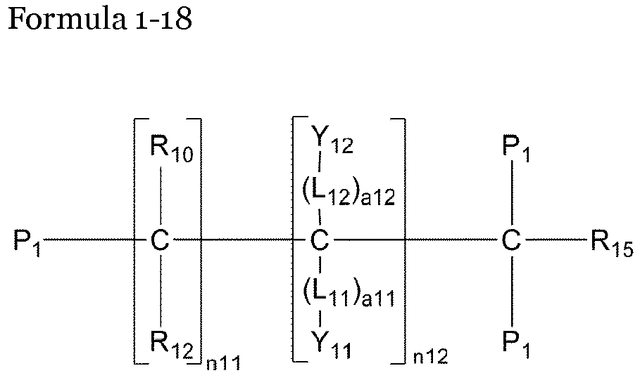
- the first compound may be represented by one of the following Formulae 1-11 to 1-18 and 2-11 to 2-18: wherein, in Formulae 1-11 to 1-18 and 2-11 to 2-18, Y 11 , Y 12 , Y 21 , and Y 22 may be each independently selected from a substituted or unsubstituted C 6 -C 60 aryl group, a substituted or unsubstituted C 6 -C 60 aryloxy group, and a substituted or unsubstituted C 6 -C 60 arylthio group; L 11 , L 12 , L 21 , and L 22 may be each independently selected from a substituted or unsubstituted C 1 -C 10 alkylene group and a substituted or unsubstituted C 2 -C 10 alkenylene group; a11, a12, a21, and a22 may be each independently selected from 0, 1, and 2; R 10 to R 19 and R 20 to R 29 may be each independently selected from hydrogen, deuterium,
- the first compound may be one of the following Compounds 101 to 106:
- the composition may further include a second compound, wherein OP of the composition for fabricating an organic film may be equal to or greater than 2.8 and equal to or less than 4.8; OP being (n 1 •OP 1 + n 2 •OP 2 ); RP of the composition for fabricating an organic film may be equal to or greater than 0.01 and equal to or less than 0.46; RP being n 1 •RP 1 ; n 1 is (number of moles of the first compound)/(number of moles of the first compound + number of moles of the second compound); n 2 is (number of moles of the second compound)/(number of moles of the first compound + number of moles of the second compound); OP 1 is (total number of atoms of the first compound) / ⁇ (number of carbon atoms of the first compound) - (number of oxygen atoms of the first compound) ⁇ ; RP 1 is ⁇ (number of carbon atoms of the substituent Y) X n ⁇ / (number of
- composition may further include an initiator.
- a viscosity of the composition may be about (1 cps) 0.001 Pa s to about (100 cps) 0.1 Pa s at 25 °C.
- the embodiments may be realized by providing an organic light-emitting display apparatus including a substrate; an organic light-emitting device on the substrate; and an encapsulation layer on the organic light-emitting device; wherein the encapsulation layer includes 1, 2, or 3 sealing units, each sealing unit including an organic film and an inorganic film that are sequentially stacked on the organic light-emitting device; the organic film includes a polymer prepared from a composition for fabricating an organic film that includes a first compound; the first compound including n substituents Y, n being selected from 1, 2, 3, and 4, and m polymerizable groups P 1 , m being selected from 1, 2, 3, and 4; wherein OP 1 of the first compound is equal to or greater than 2.8 and equal to or less than 4.8; RP 1 of the first compound is equal to or greater than 0.01 and equal to or less than 0.46; OP 1 is (total number of atoms of the first compound) / ⁇ (number of carbon atoms of the first compound) - (
- the composition for fabricating an organic film may further include a second compound, OP of the composition for fabricating an organic film is equal to or greater than 2.8 and equal to or less than 4.8, OP being (n 1 •OP 1 + n 2 •OP 2 ); RP of the composition for fabricating an organic film is equal to or greater than 0.01 and equal to or less than 0.46, RP being n 1 •RP 1 ; n 1 is (number of moles of the first compound)/(number of moles of the first compound + number of moles of the second compound); n 2 is (number of moles of the second compound)/(number of moles of the first compound + number of moles of the second compound); OP 1 is (total number of atoms of the first compound) / ⁇ (number of carbon atoms of the first compound) - (number of oxygen atoms of the first compound) ⁇ ; RP 1 is ⁇ (number of carbon atoms of the substituent Y) X n ⁇ / (num
- the inorganic film may include at least one further component selected from metal, metal nitride, metal oxide, metal oxynitride, silicon nitride, silicon oxide, and silicon oxynitride.
- the encapsulation layer may further include a lower inorganic film interposed between the organic light-emitting device and the organic film.
- the organic light-emitting display apparatus may further include at least one selected from a capping layer and a protective layer interposed between the organic light-emitting device and the encapsulation layer.
- the invention also provides a method of manufacturing an organic light-emitting display apparatus, the method including forming an organic light-emitting device on a substrate; and forming an encapsulation layer that includes 1, 2, or 3 sealing units, each of the sealing units including an organic film and an inorganic film that are sequentially stacked on the organic light-emitting device, wherein forming the encapsulation layer includes forming the organic film by applying a composition for fabricating an organic film to a region where the organic film is to be formed and polymerizing the composition, the composition including a first compound; the first compound includes n substituents Y and m polymerizable groups P 1 ; n is selected from 1, 2, 3, and 4; m is selected from 1, 2, 3, and 4; OP 1 of the first compound is equal to or greater than 2.8 and equal to or less than 4.8; OP 1 being (total number of atoms of the first compound) / ⁇ (number of carbon atoms of the first compound) - (number
- Applying the composition may include performing flash evaporation or ink-jet printing.
- Polymerizing the composition may include photocuring or thermal curing the composition.
- Forming the encapsulation layer may include forming the inorganic film by chemical vapor deposition or reactive sputtering using oxygen gas or oxygen plasma.
- FIG. 1 illustrates a cross-sectional view of an organic light-emitting display apparatus 100 according to an exemplary embodiment.
- the organic light-emitting display apparatus 100 may include a substrate 110, an organic light-emitting device 120 on the substrate 110, and an encapsulation layer 130 on the organic light-emitting device 120.
- the substrate 110 which may be a suitable substrate for organic light-emitting display apparatuses, may be, e.g., an inorganic material substrate or organic material substrate with excellent mechanical strength, thermal stability, transparency, surface smoothness, ease of handling, and waterproofness.
- the substrate 110 maybe an inorganic material substrate formed of a transparent glass material including SiO 2 as a main component.
- the substrate 110 may be, e.g., an insulating organic material substrate.
- the insulating organic material may be selected from, e.g., polyethersulphone (PES), polyacrylate (PAR), polyetherimide (PEI), polyethylene naphthalate (PEN), polyethylene terephthalate (PET), polyphenylene sulfide (PPS), polyallylate, polyimide, polycarbonate (PC), cellulose triacetate (TAC), and cellulose acetate propionate (CAP).
- PES polyethersulphone
- PAR polyacrylate
- PEI polyetherimide
- PEN polyethylene naphthalate
- PET polyethylene terephthalate
- PPS polyphenylene sulfide
- PC polycarbonate
- TAC cellulose triacetate
- CAP cellulose acetate propionate
- the organic light-emitting device 120 may be disposed on the substrate 110.
- the organic light-emitting device 120 may include a first electrode, an organic layer including an emission layer, and a second electrode.
- the first electrode may be formed on the substrate 110 by depositing or sputtering a material used to form the first electrode.
- the material used to form the first electrode may be a high work function material so as to facilitate hole injection.
- the first electrode may be a reflective electrode or a transmissive electrode.
- the material used to form the first electrode may include at least one selected from indium tin oxide (ITO), indium zinc oxide (IZO), tin oxide (SnO 2 ), zinc oxide (ZnO), silver (Ag), magnesium (Mg), aluminum (Al), aluminum-lithium (Al-Li), calcium (Ca), magnesium-indium (Mg-In), and magnesium-silver (Mg-Ag).
- the first electrode may have a single-layered or a multi-layered structure.
- the first electrode may have a triple-layered structure of ITO/Ag/ITO, without being limited thereto.
- the organic layer including the emission layer may be formed on the first electrode.
- the organic layer may include a hole transport region interposed between the first electrode and the emission layer.
- the organic layer may include an electron transport region interposed between the emission layer and the second electrode.
- the second electrode may be formed on the organic layer.
- the second electrode may be a cathode, which is an electron injecting electrode.
- a metal used to form the second electrode may be a metal having a low work function, or an alloy, an electrically conductive compound, or any mixture thereof.
- the second electrode may be a transmissive electrode formed of lithium (Li), magnesium (Mg), aluminum (Al), an Al-Li alloy, calcium (Ca), an Mg-In alloy, or an Mg-Ag alloy in a thin film.
- a transmissive electrode formed of ITO or IZO may be used, and various modifications may be applied thereto.
- the encapsulation layer 130 may be formed on the organic light-emitting device 120.
- the encapsulation layer 130 may be formed by, e.g., alternately stacking an organic film 131 and inorganic film 132.
- the encapsulation layer 130 may help reduce and/or prevent infiltration of external moisture and/or oxygen into the organic light-emitting device 120.
- the encapsulation layer 130 may include, e.g., 1, 2, or 3 sealing units each including the organic film 131 and the inorganic film 132 alternately stacked on the organic light-emitting device 120.
- one sealing unit may be included (as illustrated in FIG. 1), or 2 or 3 sealing units may be included therein.
- the organic light-emitting display apparatus 100 may include the organic light-emitting device 120, the organic film 131, and the inorganic film 132 sequentially stacked on the substrate 110.
- the organic film 131 may planarize a structure under the organic film 131 and may cover particles generated while forming a structure under the organic film 131, and reliability of the encapsulation layer 130 may be improved.
- the inorganic film 132 may substantially prevent infiltration of external moisture and/or oxygen.
- the organic film 131 may be formed of a composition for fabricating an organic film.
- the organic film 131 may include a polymer of or prepared from the composition for fabricating an organic film.
- the composition for fabricating an organic film may include a first compound including n substituents Y and m polymerizable groups P 1 , in which n may be selected from 1, 2, 3, and 4; m may be selected from 1, 2, 3, and 4.
- the first compound may include 1, 2, 3, or 4 substituents Y and 1, 2, 3, or 4 polymerizable groups P 1 .
- OP 1 of the first compound may be equal to or greater than 2.8 and equal to or less than 4.8.
- OP 1 is determined as follows: (total number of atoms of the first compound) / ⁇ (number of carbon atoms of the first compound) - (number of oxygen atoms of the first compound) ⁇ .
- RP 1 of the first compound may be equal to or greater than 0.01 and equal to or less than 0.46.
- RP 1 is determined as follows: ⁇ (number of carbon atoms of the substituent Y) X n ⁇ / (number of carbon atoms of the first compound).
- the first compound may include a monomer, an oligomer, or a mixture thereof.
- a plurality of Ys may be the same or different.
- a plurality of P 1 s may be the same or different.
- n may be 1 or 2.
- Y may be selected from or include, e.g., a substituted or unsubstituted C 6 -C 60 aryl group, a substituted or unsubstituted C 6 -C 60 aryloxy group, and a substituted or unsubstituted C 6 -C 60 arylthio group.
- Y may be, e.g., a group represented by one of the following Formulae 5-1 to 5-9.
- Formulae 5-1 to 5-9 In Formulae 5-1 to 5-9,
- R 51 may be selected from, e.g., hydrogen, a methyl group, an ethyl group, a tert-butyl group, a methoxy group, an ethoxy group, a tert-butoxy group, a phenyl group, and a naphthyl group;
- Y may be, e.g., a group represented by one of the following Formulae 5-11 to 5-28.
- * is a binding site with an adjacent atom.
- m maybe selected from, e.g., 1, 2, and 3.
- P 1 may be selected from, e.g., an acrylate group, an epoxy group, and a vinyl group.
- P 1 may be, e.g., a group represented by one of the following Formulae 6-1 to 6-3.
- Formulae 6-1 to 6-3 In Formulae 6-1 to 6-3,
- L 61 may be selected from, e.g., a methylene group and an ethylene group; a61 maybe selected from, e.g., 0, 1, 2, and 3; and/or R 61 to R 63 may each independently be selected from, e.g., hydrogen, a methyl group, an ethyl group, an n-propyl group, and a methoxy group.
- P 1 may be, e.g., a group represented by one of the following Formulae 6-1A, 6-1B, 6-1C, and 6-1D.
- Formulae 6-1A, 6-1B, 6-1C, and 6-1D are examples of Formulae 6-1A, 6-1B, 6-1C, and 6-1D.
- P 1 may be, e.g., a group represented by one of the following Formulae 6-11 to 6-18.
- * is a binding site with an adjacent atom.
- the first compound may be, e.g., represented by one of the following Formulae 1-1, 1-2, 2-1, and 2-2.
- Formulae 1-1, 1-2, 2-1, and 2-2 In Formulae 1-1, 1-2, 2-1, and 2-2,
- Y 11 , Y 12 , Y 21 , and Y 22 may each independently be, e.g., a group represented by one of the following Formulae 5-1 to 5-9.
- Formulae 5-1 to 5-9 In Formulae 5-1 to 5-9,
- L 11 , L 12 , L 21 , and L 22 may each independently be selected from, e.g., a methylene group, an ethylene group, and a propylene group.
- R 10 to R 19 and R 20 to R 29 may each independently be selected from, e.g., hydrogen, deuterium, a methyl group, an ethyl group, an n-propyl group, an iso-propyl group, an n-butyl group, an iso-butyl group, a sec-butyl group, a tert-butyl group, and a polymerizable group P 1 .
- at least one of R 10 to R 19 may be the polymerizable group P 1 and at least one of R 20 to R 29 may be the polymerizable group P 1 .
- the first compound may be, e.g., represented by one of the following Formulae 1-11 to 1-18 and 2-11 to 2-18.
- Formulae 1-11 to 1-18 and 2-11 to 2-18 are examples of the following Formulae 1-11 to 1-18 and 2-11 to 2-18.
- the first compound may be, e.g., one of the following Compounds 101 to 106.
- the first compound may have high durability against plasma.
- the inorganic film 132 is formed by PECVD or sputtering, which may degrade the organic film 131
- the first compound may provide physical properties such as viscosity that is suitable for a process of forming the organic film 131, and speed and economic efficiency of the process of forming the organic film 131 may be improved.
- the first compound may be included in the composition in an amount of about 5% by weight to about 80% by weight, e.g., about 30% by weight to about 40% by weight, based on the weight of the composition for fabricating an organic film.
- amount of the first compound is within the ranges described above, not only reliability but also manufacturing efficiency of the organic light-emitting display apparatus may be improved.
- the composition for fabricating an organic film may further include a second compound.
- OP of the composition for fabricating an organic film may be, e.g., equal to or greater than 2.8 and equal to or less than 4.8 or about 2.8 to about 4.8. OP is determined as follows (n 1 •OP 1 + n 2 •OP 2 ).
- RP of the composition for fabricating an organic film may be, e.g., equal to or greater than 0.01 and equal to or less than 0.46 or about 0.01 to about 0.46.
- RP is determined as follows n 1 •RP 1 ;
- n 1 is (number of moles of the first compound)/(number of moles of the first compound + number of moles of the second compound);
- n 2 is (number of moles of the second compound)/(number of moles of the first compound + number of moles of the second compound);
- OP 1 is (total number of atoms of the first compound) / ⁇ (number of carbon atoms of the first compound) - (number of oxygen atoms of the first compound) ⁇ ;
- RP 1 is ⁇ (number of carbon atoms of the substituent Y) X n ⁇ / (number of carbon atoms of the first compound);
- OP 2 is (total number of atoms of the second compound) /
- the second compound may be represented by one of the following Formula 3 or Formula 4.
- Formulae 3 and 4 are examples of the following Formulae 3 and 4
- the second compound may be, e.g., represented by one of the following Formulae 3-1 to 3-3, 4-1, and 4-2.
- Formulae 3-1 to 3-3, 4-1, and 4-2 are examples of the following Formulae 3-1 to 3-3, 4-1, and 4-2.
- the second compound may be, e.g., one of the following Compounds 201 to 203.:
- the second compound may serve as a starting material of polymerization together with the first compound contributing to formation of a polymer of the composition for fabricating an organic film.
- the second compound may be included in an amount of about 20% by weight to about 95% by weight, e.g., about 60% by weight to about 70% by weight, based on the weight of the composition for fabricating an organic film.
- the amount of the second compound is within the ranges described above, a rate of polymerization of the composition for fabricating an organic film may be improved and the transparency of the organic film 131 may be increased.
- the composition for fabricating an organic film may further include an initiator.
- the initiator may be a suitable material to initiate polymerization of the composition for fabricating an organic film.
- the initiator may be a thermal initiator, such as an organic peroxide-based compound and an azo-based compound, or a photo initiator such as a benzophenone-based compound, an oxime-based compound, and a phosphine oxide-based compound.
- a thermal initiator such as an organic peroxide-based compound and an azo-based compound
- a photo initiator such as a benzophenone-based compound, an oxime-based compound, and a phosphine oxide-based compound.
- organic peroxide-based compound may include benzoyl peroxide, t-butyl peroxybenzoate, o-methyl benzoyl peroxide, p-methyl benzoyl peroxide, di-t-butyl peroxide, dicumyl peroxide, 1,1-bis(t-butylperoxy)-3,3,5-trimethyl cyclohexane, 1,1-di(t-butylperoxy) cyclohexane, 2,5-dimethyl-2,5-di(t-butylperoxy)hexane, 2,5-di(t-butylperoxy)-2,5-dimethyl-hexyne, 1,6-bis(p-toluoyl peroxy carbonyloxy)hexane, and di(4-methylbenzoylperoxy) hexamethylene biscarbonate.
- Examples of the azo-based compound may include 2'-azobis (4-methoxy-2,4-dimethyl valeronitrile), 2,2'-azobis (2,4-dimethyl) valeronitrile, azobis isobutyronitrile, and 2,2'-azobis(2-methyl butyronitrile).
- benzophenone-based compound may include 2-hydroxy-2-methyl-1-phenyl-1-propanone, 2-hydroxy-1-[4-(2-hydroxyethoxy)phenyl]-2-methyl-1-propanone, alpha-dimethoxy-alpha-phenylacetophenone, 2-benzyl-2-(dimethylamino)-1-[4-(4-morpholinyl) phenyl]-1-butanone, and 2-methyl-1-[4-(methylthio)phenyl]-2-(4-morpholinyl)-1-propanone.
- Examples of the oxime-based compound may include (hydroxyimino)cyclohexane, 1-[4-(phenylthio)phenyl]-octane-1,2-dione-2-(O-benzoyloxime), 1-[9-ethyl-6-(2-methylbenzoyl)-9H-carbazol-3-yl]-ethanone-1-(O-acetyloxime), trichloromethyl-triazine derivatives, 4-(4-methoxystyryl)-2,6-trichloromethyl-1,3,5-triazine, 4-(4-methoxyphenyl)-2,6-trichloromethyl-1,3,5-triazine, and ⁇ - aminoketone (1-(4-morpholinophenyl)-2-dimethylamino-2-benzyl-butan-1-one).
- phosphine oxide-based compound may include diphenyl(2,4,6-trimethylbenzoyl)-phosphine oxide (TPO) and phenyl bis (2,4,6-trimethyl benzoyl) phosphine oxide (BAPO).
- TPO diphenyl(2,4,6-trimethylbenzoyl)-phosphine oxide
- BAPO phenyl bis (2,4,6-trimethyl benzoyl) phosphine oxide
- An amount of the initiator may be selected within a suitable range.
- the initiator may be included in an amount of, e.g., about 0.01% by weight to about 10% by weight, based on the weight of the composition for fabricating an organic film.
- the viscosity of the composition for fabricating an organic film may be in a range of about (1 cps) 0.001 Pa s to about (100 cps) 0.1 Pa s at 25 °C, e.g., about (10 cps) 0.01 Pa s to about (50 cps) 0.05 Pa s at 25 °C.
- the viscosity of the composition for fabricating an organic film is within the ranges described above, ease of manufacturing the composition for fabricating an organic film may be improved and the polymer of the composition for fabricating an organic film may have excellent planarization properties.
- the thickness of the organic film 131 may be in a range of about 0.1 ⁇ m to about 50 ⁇ m, e.g., about 1 ⁇ m to about 10 ⁇ m. When the thickness of the organic film 131 is within the ranges described above, planarization of the structure under the organic film 131 may be efficiently performed.
- composition for fabricating an organic film may be applied to a region where the organic film will be formed using suitable methods such as flash evaporation, spin coating, dip coating, or ink-jet printing, without being limited thereto.
- suitable methods such as flash evaporation, spin coating, dip coating, or ink-jet printing, without being limited thereto.
- the composition for fabricating an organic film may be applied to the region where the organic film will be formed by flash evaporation or ink-jet printing.
- the composition for fabricating an organic film applied to the region may be polymerized by, e.g., photocuring or thermal curing.
- the composition for fabricating an organic film may be polymerized by known methods such as UV curing, infrared curing, and laser curing.
- the inorganic film 132 may include an inorganic material suitable for forming encapsulation layers.
- the inorganic film 132 may include at least one selected from metal, metal nitride, metal oxide, metal oxynitride, silicon nitride, silicon oxide, and silicon oxynitride.
- the inorganic film 132 may include at least one selected from aluminum oxide, silicon oxide, silicon nitride, and silicon oxynitride.
- a thickness of the inorganic film 132 may be in a range of about (100 ⁇ ) 10nm to about (15,000 ⁇ ) 1,500nm, e.g., about (500 ⁇ ) 50nm to about (3,000 ⁇ ) 300nm.
- the encapsulation layer 130 may efficiently block moisture and/or oxygen.
- the inorganic film 132 may be formed by, e.g., sputtering, reactive sputtering, chemical vapor deposition (CVD), plasma-enhanced chemical vapor deposition (PECVD), evaporation, electron cyclotron resonance PECVD, physical vapor deposition, atomic layer deposition (ALD), or the like.
- the inorganic film 132 may be formed by reactive sputtering by using oxygen gas or oxygen plasma or CVD.
- the encapsulation layer 130 may further include a lower inorganic film interposed between the organic light-emitting device 120 and the organic film 131.
- the lower inorganic film may enhance the ability of the encapsulation layer 130 to block moisture and/or oxygen.
- the lower inorganic film is as described above with reference to the inorganic film 132.
- a thickness of the encapsulation layer 130 may be in a range of about 0.1 ⁇ m to about 1,000 ⁇ m, e.g., about 1 ⁇ m to about 10 ⁇ m.
- the encapsulation layer 130 may efficiently block infiltration of moisture and/or oxygen into the organic light-emitting device 120 and may have flexibility.
- At least one of a capping layer and a protective layer may further be interposed between the organic light-emitting device 120 and the encapsulation layer 130.
- the capping layer may be formed on the organic light-emitting device 120.
- the capping layer may induce constructive interference of light emitted from the organic light-emitting device 120, thereby increasing light coupling efficiency.
- the capping layer may be formed of a material having a relatively high refractive index, e.g., an organic metal complex such as Alq 3 , silicon oxide, and silicon nitride.
- the protective layer may be formed on the capping layer or the organic light-emitting device 120.
- the protective layer may help prevent damage of the capping layer or damage of the organic light-emitting device 120 caused during the formation of the encapsulation layer 130.
- the protective layer may include lithium fluoride, silicon oxide, silicon nitride, and the like.
- an upper inorganic film may further be formed on the encapsulation layer 130.
- the upper inorganic film may enhance adhesive force between a film to be attached to the organic light-emitting display apparatus 100 and the organic light-emitting display apparatus 100.
- the upper inorganic film is as described above with reference to the inorganic film 132.
- FIG. 2 illustrates a cross-sectional view of an organic light-emitting display apparatus 200 according to another exemplary embodiment.
- the organic light-emitting display apparatus 200 may include a substrate 210, an organic light-emitting device 200 on the substrate 210, and an encapsulation layer on the organic light-emitting device 220.
- the encapsulation layer may include a first sealing unit 230 and a second sealing unit 240.
- the first sealing unit 230 may include a first organic film 231 and a first inorganic film 232 that are sequentially stacked on the organic light-emitting device 220.
- the second sealing unit 240 may include a second organic film 241 and a second inorganic film 242 that are sequentially stacked on the first sealing unit 230.
- the first organic film 231 and the second organic film 241 may be as described above with reference to the organic film 131.
- a thickness of the first organic film 231 may be the same as or different from that of the second organic film 241.
- Materials used to form the first organic film 231 and the second organic film 241 may be the same or different.
- the first inorganic film 232 and the second inorganic film 242 are as described above with reference to the inorganic film 132.
- a thickness of the first inorganic film 232 may be the same as or different from that of the second inorganic film 242.
- Materials used to form the first inorganic film 232 and the second inorganic film 242 may be the same or different.
- the invention comprises a method of manufacturing the organic light-emitting display apparatus 100.
- An organic light-emitting device 120 may be formed on a substrate 110.
- the organic light-emitting device 120 may be formed using a suitable method.
- a lower inorganic film may be formed on the organic light-emitting device 120 to cover the organic light-emitting device 120.
- the lower inorganic film is as described above.
- a composition for fabricating an organic film may be applied to the lower inorganic film at a region where an organic film will be formed and polymerized to form an organic film 131.
- the composition for fabricating an organic film is as described above and the organic film 131 is as described above.
- An inorganic film 132 may be formed on the organic film 131.
- the inorganic film 132 is as described above.
- an organic light-emitting display apparatus including one or two sealing units is described above.
- the encapsulation layer includes two or more encapsulation layers
- another layer e.g., an organic film and an inorganic film contained in an encapsulation layer of a conventional organic light-emitting display apparatus, may further be interposed between the encapsulation layers, and various other modifications may also be applied thereto.
- a composition for fabricating an organic film was prepared by mixing compounds listed in Table 1 below in a weight ratio described in Table 1.
- Table 1 First compound Second compound Initiator Example 1
- Compound 102 (33.98% by weight)
- Compound 203 (63.11% by weight)
- TPO (2.91% by weight)
- Viscosity of the composition for fabricating an organic film was measured using a Brookfield DE-II +Pro viscometer at 25 °C, and the results are shown in Table 2 below. Table 2 Viscosity (cps) Pa s Example 1 (20) 0.020
- a composition for fabricating an organic film was prepared by mixing compounds listed in Table 3 below in a weight ratio described in Table 3.
- Table 3 First compound Second compound Initiator Comparative Example 1 - Compound 203 (90.90% by weight), trimethylol propane triacrylate (4.79% by weight) TPO (4.31% by weight) Comparative Example 2 Compound 102 (1.94% by weight) Compound 203 (95.15% by weight) TPO (2.91% by weight)
- Viscosity of the composition for fabricating an organic film was measured using a Brookfield DE-II +Pro viscometer at 25 °C, and the results are shown in Table 4 below.
- Table 4 Viscosity (cps) Pa s Comparative Example 1 (14) 0.014 Comparative Example 2 (15) 0.015
- a glass substrate on which 500 organic light-emitting devices were formed was prepared.
- a glass capping layer having a thickness of (800 ⁇ ) 80nm was formed to cover the organic light-emitting devices, and LiF was deposited on the capping layer to form a protective layer.
- an organic light-emitting display apparatus was manufactured by preparing an encapsulation layer by forming:
- An organic light-emitting display apparatus was manufactured in the same manner as in Example 2, except that the composition of Comparative Example 1 was used in the formation of the organic film, instead of the composition of Example 1.
- the organic light-emitting display apparatus according to Example 2 exhibited excellent lifespan characteristics due to high durability against oxygen plasma, as compared with the organic light-emitting display apparatus according to Comparative Example 3.
- the organic light-emitting display apparatus may further include a driving transistor or a switching transistor.
- An organic light-emitting device may be deteriorated by oxygen and/or moisture, and a sealing member may further be applied to the organic light-emitting device.
- the organic light-emitting display apparatus has high stability during the plasma process.
- the embodiments may provide compositions for fabricating an organic film having high stability in a plasma process.
Landscapes
- Chemical & Material Sciences (AREA)
- Organic Chemistry (AREA)
- Life Sciences & Earth Sciences (AREA)
- Engineering & Computer Science (AREA)
- Materials Engineering (AREA)
- Wood Science & Technology (AREA)
- Health & Medical Sciences (AREA)
- Chemical Kinetics & Catalysis (AREA)
- Medicinal Chemistry (AREA)
- Polymers & Plastics (AREA)
- Inorganic Chemistry (AREA)
- Physics & Mathematics (AREA)
- Optics & Photonics (AREA)
- Electroluminescent Light Sources (AREA)
Abstract
Description
- The present invention relates to compositions for fabricating an organic film, organic light-emitting display apparatuses manufactured using the same, and methods of manufacturing the organic light-emitting display apparatuses.
- Organic light-emitting devices, which are self-emitting devices, have advantages such as wide viewing angles, excellent contrast, quick response, high brightness, and excellent driving voltage characteristics, and can provide multicolored images.
- An organic light-emitting device may have a structure including a substrate, and a first electrode, a hole transport region, an emission layer, an electron transport region, and a second electrode, which are sequentially disposed on the substrate. Holes injected from the first electrode move to the emission layer via the hole transport region, and electrons injected from the second electrode move to the emission layer via the electron transport region. Carriers such as the holes and electrons recombine in the emission layer to generate excitons. When the excitons drop from an excited state to a ground state, light is emitted.
- Accordingly, a first aspect of the present invention is directed to compositions for fabricating an organic film, organic light-emitting display apparatuses manufactured using the same, and methods of manufacturing the organic light-emitting display apparatuses.
- The invention may be realized by providing a composition for fabricating an organic film, the composition including a first compound that includes n substituents Y, and m polymerizable groups P1, wherein n is selected from 1, 2, 3, and 4; m is selected from 1, 2, 3, and 4; OP1 of the first compound is equal to or greater than 2.8 and equal to or less than 4.8; OP1 being (total number of atoms of the first compound) / {(number of carbon atoms of the first compound) - (number of oxygen atoms of the first compound)}; and RP1 of the first compound is equal to or greater than 0.01 and equal to or less than 0.46; RP1 being {(number of carbon atoms of the substituent Y) X n} / (number of carbon atoms of the first compound). Y may be selected from a substituted or unsubstituted C6-C60 aryl group, a substituted or unsubstituted C6-C60 aryloxy group, and a substituted or unsubstituted C6-C60 arylthio group. m may be selected from 1, 2, and 3.
- P1 may be selected from an acrylate group, an epoxy group, and a vinyl group.
- P1 may be a group represented by one of the following Formulae 6-1 to 6-3:

- The first compound may be represented by one of the following Formulae 1-1, 1-2, 2-1, and 2-2:


- The first compound may be represented by one of the following Formulae 1-11 to 1-18 and 2-11 to 2-18:




- The first compound may be one of the following Compounds 101 to 106:


- The composition may further include a second compound, wherein OP of the composition for fabricating an organic film may be equal to or greater than 2.8 and equal to or less than 4.8; OP being (n1•OP1 + n2•OP2); RP of the composition for fabricating an organic film may be equal to or greater than 0.01 and equal to or less than 0.46; RP being n1•RP1; n1 is (number of moles of the first compound)/(number of moles of the first compound + number of moles of the second compound); n2 is (number of moles of the second compound)/(number of moles of the first compound + number of moles of the second compound); OP1 is (total number of atoms of the first compound) / {(number of carbon atoms of the first compound) - (number of oxygen atoms of the first compound)}; RP1 is {(number of carbon atoms of the substituent Y) X n} / (number of carbon atoms of the first compound); and OP2 is (total number of atoms of the second compound) / {(number of carbon atoms of the second compound) - (number of oxygen atoms of the second compound)}.
- The composition may further include an initiator.
- A viscosity of the composition may be about (1 cps) 0.001 Pa s to about (100 cps) 0.1 Pa s at 25 °C.
- The embodiments may be realized by providing an organic light-emitting display apparatus including a substrate; an organic light-emitting device on the substrate; and an encapsulation layer on the organic light-emitting device; wherein the encapsulation layer includes 1, 2, or 3 sealing units, each sealing unit including an organic film and an inorganic film that are sequentially stacked on the organic light-emitting device; the organic film includes a polymer prepared from a composition for fabricating an organic film that includes a first compound; the first compound including n substituents Y, n being selected from 1, 2, 3, and 4, and m polymerizable groups P1, m being selected from 1, 2, 3, and 4; wherein OP1 of the first compound is equal to or greater than 2.8 and equal to or less than 4.8; RP1 of the first compound is equal to or greater than 0.01 and equal to or less than 0.46; OP1 is (total number of atoms of the first compound) / {(number of carbon atoms of the first compound) - (number of oxygen atoms of the first compound)}; and RP1 is {(number of carbon atoms of the substituent Y) X n} / (number of carbon atoms of the first compound).
- The composition for fabricating an organic film may further include a second compound, OP of the composition for fabricating an organic film is equal to or greater than 2.8 and equal to or less than 4.8, OP being (n1•OP1 + n2•OP2); RP of the composition for fabricating an organic film is equal to or greater than 0.01 and equal to or less than 0.46, RP being n1•RP1; n1 is (number of moles of the first compound)/(number of moles of the first compound + number of moles of the second compound); n2 is (number of moles of the second compound)/(number of moles of the first compound + number of moles of the second compound); OP1 is (total number of atoms of the first compound) / {(number of carbon atoms of the first compound) - (number of oxygen atoms of the first compound)}; RP1 is {(number of carbon atoms of the substituent Y) X n} / (number of carbon atoms of the first compound); and OP2 is (total number of atoms of the second compound) / {(number of carbon atoms of the second compound) - (number of oxygen atoms of the second compound)}.
- The inorganic film may include at least one further component selected from metal, metal nitride, metal oxide, metal oxynitride, silicon nitride, silicon oxide, and silicon oxynitride.
- The encapsulation layer may further include a lower inorganic film interposed between the organic light-emitting device and the organic film.
- The organic light-emitting display apparatus may further include at least one selected from a capping layer and a protective layer interposed between the organic light-emitting device and the encapsulation layer.
- According to a further aspect, the invention also provides a method of manufacturing an organic light-emitting display apparatus, the method including forming an organic light-emitting device on a substrate; and forming an encapsulation layer that includes 1, 2, or 3 sealing units, each of the sealing units including an organic film and an inorganic film that are sequentially stacked on the organic light-emitting device, wherein forming the encapsulation layer includes forming the organic film by applying a composition for fabricating an organic film to a region where the organic film is to be formed and polymerizing the composition, the composition including a first compound; the first compound includes n substituents Y and m polymerizable groups P1; n is selected from 1, 2, 3, and 4; m is selected from 1, 2, 3, and 4; OP1 of the first compound is equal to or greater than 2.8 and equal to or less than 4.8; OP1 being (total number of atoms of the first compound) / {(number of carbon atoms of the first compound) - (number of oxygen atoms of the first compound)}; and RP1 of the first compound is equal to or greater than 0.01 and equal to or less than 0.46; RP1 being {(number of carbon atoms of the substituent Y) X n} / (number of carbon atoms of the first compound).
- Applying the composition may include performing flash evaporation or ink-jet printing.
- Polymerizing the composition may include photocuring or thermal curing the composition.
- Forming the encapsulation layer may include forming the inorganic film by chemical vapor deposition or reactive sputtering using oxygen gas or oxygen plasma.
- These and/or other aspects will become apparent and more readily appreciated from the following description of the embodiments taken in conjunction with the accompanying drawings in which:
-
FIG. 1 illustrates a cross-sectional view of an organic light-emitting display apparatus according to an exemplary embodiment; and -
FIG. 2 illustrates a cross-sectional view of an organic light-emitting display apparatus according to another exemplary embodiment. - Example embodiments will now be described more fully hereinafter with reference to the accompanying drawings; however, they may be embodied in different forms and should not be construed as limited to the embodiments set forth herein. Rather, these embodiments are provided so that this disclosure will be thorough and complete, and will fully convey exemplary implementations to those skilled in the art.
-
FIG. 1 illustrates a cross-sectional view of an organic light-emittingdisplay apparatus 100 according to an exemplary embodiment. - The organic light-
emitting display apparatus 100 may include asubstrate 110, an organic light-emitting device 120 on thesubstrate 110, and an encapsulation layer 130 on the organic light-emitting device 120. - The
substrate 110, which may be a suitable substrate for organic light-emitting display apparatuses, may be, e.g., an inorganic material substrate or organic material substrate with excellent mechanical strength, thermal stability, transparency, surface smoothness, ease of handling, and waterproofness. - For example, the
substrate 110 maybe an inorganic material substrate formed of a transparent glass material including SiO2 as a main component. - In an example, the
substrate 110 may be, e.g., an insulating organic material substrate. The insulating organic material may be selected from, e.g., polyethersulphone (PES), polyacrylate (PAR), polyetherimide (PEI), polyethylene naphthalate (PEN), polyethylene terephthalate (PET), polyphenylene sulfide (PPS), polyallylate, polyimide, polycarbonate (PC), cellulose triacetate (TAC), and cellulose acetate propionate (CAP). - The organic light-
emitting device 120 may be disposed on thesubstrate 110. The organic light-emitting device 120 may include a first electrode, an organic layer including an emission layer, and a second electrode. - The first electrode may be formed on the
substrate 110 by depositing or sputtering a material used to form the first electrode. When the first electrode constitutes an anode, the material used to form the first electrode may be a high work function material so as to facilitate hole injection. The first electrode may be a reflective electrode or a transmissive electrode. The material used to form the first electrode may include at least one selected from indium tin oxide (ITO), indium zinc oxide (IZO), tin oxide (SnO2), zinc oxide (ZnO), silver (Ag), magnesium (Mg), aluminum (Al), aluminum-lithium (Al-Li), calcium (Ca), magnesium-indium (Mg-In), and magnesium-silver (Mg-Ag). - The first electrode may have a single-layered or a multi-layered structure. For example, the first electrode may have a triple-layered structure of ITO/Ag/ITO, without being limited thereto.
- The organic layer including the emission layer may be formed on the first electrode.
- The organic layer may include a hole transport region interposed between the first electrode and the emission layer. The organic layer may include an electron transport region interposed between the emission layer and the second electrode.
- The second electrode may be formed on the organic layer. The second electrode may be a cathode, which is an electron injecting electrode. A metal used to form the second electrode may be a metal having a low work function, or an alloy, an electrically conductive compound, or any mixture thereof. For example, the second electrode may be a transmissive electrode formed of lithium (Li), magnesium (Mg), aluminum (Al), an Al-Li alloy, calcium (Ca), an Mg-In alloy, or an Mg-Ag alloy in a thin film. In order to manufacture a top emission-type organic light-emitting device, a transmissive electrode formed of ITO or IZO may be used, and various modifications may be applied thereto.
- The encapsulation layer 130 may be formed on the organic light-
emitting device 120. The encapsulation layer 130 may be formed by, e.g., alternately stacking an organic film 131 and inorganic film 132. The encapsulation layer 130 may help reduce and/or prevent infiltration of external moisture and/or oxygen into the organic light-emitting device 120. - The encapsulation layer 130 may include, e.g., 1, 2, or 3 sealing units each including the organic film 131 and the inorganic film 132 alternately stacked on the organic light-
emitting device 120. In an implementation, one sealing unit may be included (as illustrated inFIG. 1), or 2 or 3 sealing units may be included therein. When the encapsulation layer 130 includes one sealing unit, the organic light-emittingdisplay apparatus 100 may include the organic light-emittingdevice 120, the organic film 131, and the inorganic film 132 sequentially stacked on thesubstrate 110. - The organic film 131 may planarize a structure under the organic film 131 and may cover particles generated while forming a structure under the organic film 131, and reliability of the encapsulation layer 130 may be improved.
- The inorganic film 132 may substantially prevent infiltration of external moisture and/or oxygen.
- The organic film 131 may be formed of a composition for fabricating an organic film. For example, the organic film 131 may include a polymer of or prepared from the composition for fabricating an organic film.
- The composition for fabricating an organic film may include a first compound including n substituents Y and m polymerizable groups P1, in which n may be selected from 1, 2, 3, and 4; m may be selected from 1, 2, 3, and 4. For example, the first compound may include 1, 2, 3, or 4 substituents Y and 1, 2, 3, or 4 polymerizable groups P1.
- OP1 of the first compound may be equal to or greater than 2.8 and equal to or less than 4.8. For example, OP1 is determined as follows: (total number of atoms of the first compound) / {(number of carbon atoms of the first compound) - (number of oxygen atoms of the first compound)}.
- RP1 of the first compound may be equal to or greater than 0.01 and equal to or less than 0.46. For example, RP1 is determined as follows: {(number of carbon atoms of the substituent Y) X n} / (number of carbon atoms of the first compound).
- The first compound may include a monomer, an oligomer, or a mixture thereof.
- In the first compound, when n is 2 or greater, a plurality of Ys may be the same or different.
- In the first compound, when m is 2 or greater, a plurality of P1s may be the same or different.
- For example, n may be 1 or 2.
- In an implementation, Y may be selected from or include, e.g., a substituted or unsubstituted C6-C60 aryl group, a substituted or unsubstituted C6-C60 aryloxy group, and a substituted or unsubstituted C6-C60 arylthio group.
- In an implementation, Y may be, e.g., a group represented by one of the following Formulae 5-1 to 5-9.


- R51 may be selected from, e.g., hydrogen, deuterium, -F, -Cl, -Br, -I, a cyano group, a nitro group, a C1-C10 alkyl group, a C1-C10 alkoxy group, and a C6-C30 aryl group; a51 may be selected from, e.g., 1, 2, 3, 4, and 5;
- a52 may be selected from, e.g., 1, 2, 3, 4, 5, 6, and 7; and
- * is a binding site with an adjacent atom.
- In an implementation, in Formulae 5-1 to 5-9, R51 may be selected from, e.g., hydrogen, a methyl group, an ethyl group, a tert-butyl group, a methoxy group, an ethoxy group, a tert-butoxy group, a phenyl group, and a naphthyl group;
- In an implementation, Y may be, e.g., a group represented by one of the following Formulae 5-11 to 5-28.


- In Formulae 5-11 to 5-28, * is a binding site with an adjacent atom.
- In an implementation, m maybe selected from, e.g., 1, 2, and 3.
- In an implementation, P1 may be selected from, e.g., an acrylate group, an epoxy group, and a vinyl group.
- In an implementation, P1 may be, e.g., a group represented by one of the following Formulae 6-1 to 6-3.

- L61 may be selected from or include, e.g., a substituted or unsubstituted C1-C10 alkylene group and a substituted or unsubstituted C2-C10 alkenylene group;
- a61 may be selected from, e.g., 0, 1, 2, 3, 4, and 5;
- R61 to R63 may each independently be selected from or include, e.g., hydrogen, a substituted or unsubstituted C1-C10 alkyl group, and a substituted or unsubstituted C1-C10 alkoxy group; and
- * is a binding site with an adjacent atom.
- In an implementation, in Formulae 6-1 to 6-3, L61 may be selected from, e.g., a methylene group and an ethylene group; a61 maybe selected from, e.g., 0, 1, 2, and 3; and/or R61 to R63 may each independently be selected from, e.g., hydrogen, a methyl group, an ethyl group, an n-propyl group, and a methoxy group.
- In an implementation, P1 may be, e.g., a group represented by one of the following Formulae 6-1A, 6-1B, 6-1C, and 6-1D.

- R61 may be selected from, e.g., hydrogen, a methyl group, an ethyl group, and an n-propyl group; and
- * is a binding site with an adjacent atom.
- In an implementation, P1 may be, e.g., a group represented by one of the following Formulae 6-11 to 6-18.


- In Formulae 6-11 to 6-18, * is a binding site with an adjacent atom.
- In an implementation, the first compound may be, e.g., represented by one of the following Formulae 1-1, 1-2, 2-1, and 2-2.


- Y11, Y12, Y21, and Y22 may each independently be selected from or include, e.g., a substituted or unsubstituted C6-C60 aryl group, a substituted or unsubstituted C6-C60 aryloxy group, and a substituted or unsubstituted C6-C60 arylthio group;
- L11, L12, L21, and L22 may each independently be selected from or include, e.g., a substituted or unsubstituted C1-C10 alkylene group and a substituted or unsubstituted C2-C10 alkenylene group;
- a11, a12, a21, and a22 may each independently be selected from 0, 1, and 2;
- R10 to R19 and R20 to R29 may each independently be selected from or include, e.g., hydrogen, deuterium, a substituted or unsubstituted C1-C10 alkyl group, a substituted or unsubstituted C3-C10 cycloalkyl group, and a polymerizable group P1. In an implementation, at least one of R10 to R19 may be the polymerizable group P1 and at least one of R20 to R29 is the polymerizable group P1.
- n11 to n15 and n21 to n25 may each independently be selected from 0, 1, 2, 3, 4, and 5; a sum of n12 and n14 may be 1 or 2; and
- a sum of n22 and n24 may be 1 or 2.
- In an embodiment of the invention, in Formulae 1-1, 1-2, 2-1, and 2-2, Y11, Y12, Y21, and Y22 may each independently be, e.g., a group represented by one of the following Formulae 5-1 to 5-9.


- R51 may be selected from, e.g., hydrogen, deuterium, -F, -Cl, -Br, -I, a cyano group, a nitro group, a C1-C10 alkyl group, a C1-C10 alkoxy group, and a C6-C30 aryl group; a51 may be selected from 1, 2, 3, 4, and 5;
- a52 may be selected from 1, 2, 3, 4, 5, 6, and 7; and
- * is a binding site with an adjacent atom.
- In an embodiment of the invention, in Formulae 1-1, 1-2, 2-1, and 2-2, L11, L12, L21, and L22 may each independently be selected from, e.g., a methylene group, an ethylene group, and a propylene group.
- In an embodiment of the invention, in Formulae 1-1, 1-2, 2-1, and 2-2, R10 to R19 and R20 to R29 may each independently be selected from, e.g., hydrogen, deuterium, a methyl group, an ethyl group, an n-propyl group, an iso-propyl group, an n-butyl group, an iso-butyl group, a sec-butyl group, a tert-butyl group, and a polymerizable group P1. In an implementation, at least one of R10 to R19 may be the polymerizable group P1 and at least one of R20 to R29 may be the polymerizable group P1.
- In an embodiment of the invention, the first compound may be, e.g., represented by one of the following Formulae 1-11 to 1-18 and 2-11 to 2-18.
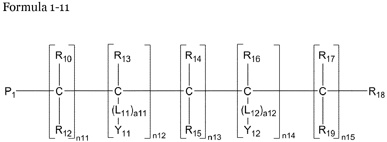


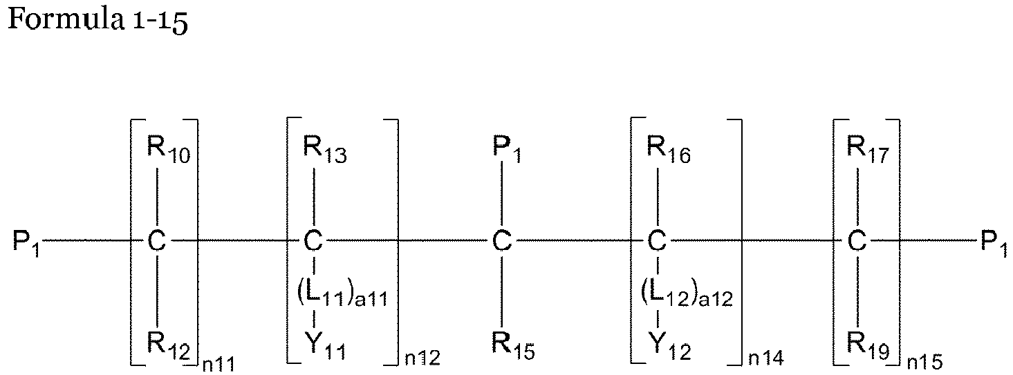


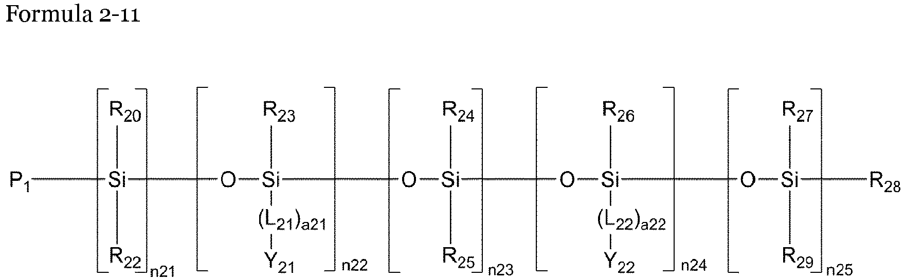


- Y11, Y12, Y21, and Y22 may each independently be selected from or include, e.g., a substituted or unsubstituted C6-C60 aryl group, a substituted or unsubstituted C6-C60 aryloxy group, and a substituted or unsubstituted C6-C60 arylthio group;
- L11, L12, L21, and L22 may each independently be selected from or include, e.g., a substituted or unsubstituted C1-C10 alkylene group and a substituted or unsubstituted C2-C10 alkenylene group;
- a11, a12, a21, and a22 may each independently be selected from 0, 1, and 2; R10 to R19 and R20 to R29 may each independently be selected from or include, e.g., hydrogen, deuterium, a substituted or unsubstituted C1-C10 alkyl group, and a substituted or unsubstituted C3-C10 cycloalkyl group; and
- P1 may be, e.g., a group represented by one of the following Formulae 6-1 to 6-3.
- L61 may be selected from or include, e.g., a substituted or unsubstituted C1-C10 alkylene group and a substituted or unsubstituted C2-C10 alkenylene group;
- a61 may be selected from 0, 1, 2, and 3;
- R61 to R63 may each independently be selected from or include, e.g., hydrogen, a substituted or unsubstituted C1-C10 alkyl group, and a substituted or unsubstituted C1-C10 alkoxy group;
- * is a binding site with an adjacent atom;
- n11 to n15 and n21 to n25 may each independently be selected from 0, 1, 2, 3, 4, and 5; a sum of n12 and n14 may be 1 or 2; and
- a sum of n22 and n24 may be 1 or 2.
- In an embodiment of the invention, the first compound may be, e.g., one of the following Compounds 101 to 106.


- The first compound may have high durability against plasma. Thus, when the inorganic film 132 is formed by PECVD or sputtering, which may degrade the organic film 131, after forming the organic film 131 by using the composition for fabricating an organic film including the first compound, degradation of the organic film 131 may be inhibited. In addition, the first compound may provide physical properties such as viscosity that is suitable for a process of forming the organic film 131, and speed and economic efficiency of the process of forming the organic film 131 may be improved.
- The first compound may be included in the composition in an amount of about 5% by weight to about 80% by weight, e.g., about 30% by weight to about 40% by weight, based on the weight of the composition for fabricating an organic film. When the amount of the first compound is within the ranges described above, not only reliability but also manufacturing efficiency of the organic light-emitting display apparatus may be improved.
- In an embodiment of the invention, the composition for fabricating an organic film may further include a second compound.
- OP of the composition for fabricating an organic film may be, e.g., equal to or greater than 2.8 and equal to or less than 4.8 or about 2.8 to about 4.8. OP is determined as follows (n1•OP1 + n2•OP2).
- RP of the composition for fabricating an organic film may be, e.g., equal to or greater than 0.01 and equal to or less than 0.46 or about 0.01 to about 0.46. RP is determined as follows n1•RP1;
n1 is (number of moles of the first compound)/(number of moles of the first compound + number of moles of the second compound);
n2 is (number of moles of the second compound)/(number of moles of the first compound + number of moles of the second compound);
OP1 is (total number of atoms of the first compound) / {(number of carbon atoms of the first compound) - (number of oxygen atoms of the first compound)};
RP1 is {(number of carbon atoms of the substituent Y) X n} / (number of carbon atoms of the first compound); and
OP2 is (total number of atoms of the second compound) / {(number of carbon atoms of the second compound) - (number of oxygen atoms of the second compound)}, without being limited thereto. - In an embodiment of the invention, the second compound may be represented by one of the following Formula 3 or Formula 4.


- R30 to R34 and R40 to R45 may each independently be selected from or include, e.g., hydrogen, deuterium, a substituted or unsubstituted C1-C10 alkyl group, a substituted or unsubstituted C3-C10 cycloalkyl group, and a polymerizable group P2. In an implementation, at least one of R30 to R34 may be the polymerizable group P2 and at least one of R40 to R45 may be the polymerizable group P2.
- P2 may be selected from, e.g., an acrylate group, an epoxy group, and a vinyl group; and
- n31, n41, and n42 may each independently be selected from integers from 0 to 20. In an embodiment of the invention, in Formulae 3 and 4,
- R30 to R34 and R40 to R45 may each independently be selected from, e.g., hydrogen, deuterium, a methyl group, an ethyl group, an n-propyl group, an iso-propyl group, an n-butyl group, an iso-butyl group, a sec-butyl group, a tert-butyl group, and a polymerizable group P2. In an implementation, at least one of R30 to R34 may be the polymerizable group P2 and at least one of R40 to R45 may be the polymerizable group P2.
- P2 may be, e.g., a group represented by one of the following Formulae 6-1 to 6-3.
- L61 may be selected from or include, e.g., a substituted or unsubstituted C1-C10 alkylene group and a substituted or unsubstituted C2-C10 alkenylene group;
- a61 may be selected from 0, 1, 2, 3, 4, and 5;
- R61 to R63 may each independently be selected from or include, e.g., hydrogen, a substituted or unsubstituted C1-C10 alkyl group, and a substituted or unsubstituted C1-C10 alkoxy group;
- * is a binding site with an adjacent atom; and
- n31, n41, and n42 may each independently be selected from integers from 0 to 15.
- In an embodiment of the invention, the second compound may be, e.g., represented by one of the following Formulae 3-1 to 3-3, 4-1, and 4-2.


- R30 to R34 and R40 to R45 may each independently be selected from, e.g., hydrogen, deuterium, a methyl group, an ethyl group, an n-propyl group, an iso-propyl group, an n-butyl group, an iso-butyl group, a sec-butyl group, a tert-butyl group, and a polymerizable group P2. In an implementation, at least one of R30 to R34 may be the polymerizable group P2 and at least one of R40 to R45 may be the polymerizable group P2.
- P2 may be, e.g., a group represented by one of the following Formulae 6-1 to 6-3.
- L61 may be selected from or include, e.g., a substituted or unsubstituted C1-C10 alkylene group and a substituted or unsubstituted C2-C10 alkenylene group;
- a61 may be selected from 0, 1, 2, and 3;
- R61 to R63 may each independently be selected from or include, e.g., hydrogen, a substituted or unsubstituted C1-C10 alkyl group, and a substituted or unsubstituted C1-C10 alkoxy group;
- * is a binding site with an adjacent atom; and
- n31, n41, and n42 may each independently be selected from integers from 0 to 15.
- In an embodiment of the invention, the second compound may be, e.g., one of the following Compounds 201 to 203.:


- The second compound may serve as a starting material of polymerization together with the first compound contributing to formation of a polymer of the composition for fabricating an organic film.
- When the composition for fabricating an organic film includes the second compound as described above, the second compound may be included in an amount of about 20% by weight to about 95% by weight, e.g., about 60% by weight to about 70% by weight, based on the weight of the composition for fabricating an organic film. When the amount of the second compound is within the ranges described above, a rate of polymerization of the composition for fabricating an organic film may be improved and the transparency of the organic film 131 may be increased.
- In an embodiment of the invention, the composition for fabricating an organic film may further include an initiator. The initiator may be a suitable material to initiate polymerization of the composition for fabricating an organic film.
- In an embodiment of the invention, the initiator may be a thermal initiator, such as an organic peroxide-based compound and an azo-based compound, or a photo initiator such as a benzophenone-based compound, an oxime-based compound, and a phosphine oxide-based compound.
- Examples of the organic peroxide-based compound may include benzoyl peroxide, t-butyl peroxybenzoate, o-methyl benzoyl peroxide, p-methyl benzoyl peroxide, di-t-butyl peroxide, dicumyl peroxide, 1,1-bis(t-butylperoxy)-3,3,5-trimethyl cyclohexane, 1,1-di(t-butylperoxy) cyclohexane, 2,5-dimethyl-2,5-di(t-butylperoxy)hexane, 2,5-di(t-butylperoxy)-2,5-dimethyl-hexyne, 1,6-bis(p-toluoyl peroxy carbonyloxy)hexane, and di(4-methylbenzoylperoxy) hexamethylene biscarbonate.
- Examples of the azo-based compound may include 2'-azobis (4-methoxy-2,4-dimethyl valeronitrile), 2,2'-azobis (2,4-dimethyl) valeronitrile, azobis isobutyronitrile, and 2,2'-azobis(2-methyl butyronitrile).
- Examples of the benzophenone-based compound may include 2-hydroxy-2-methyl-1-phenyl-1-propanone, 2-hydroxy-1-[4-(2-hydroxyethoxy)phenyl]-2-methyl-1-propanone, alpha-dimethoxy-alpha-phenylacetophenone, 2-benzyl-2-(dimethylamino)-1-[4-(4-morpholinyl) phenyl]-1-butanone, and 2-methyl-1-[4-(methylthio)phenyl]-2-(4-morpholinyl)-1-propanone.
- Examples of the oxime-based compound may include (hydroxyimino)cyclohexane, 1-[4-(phenylthio)phenyl]-octane-1,2-dione-2-(O-benzoyloxime), 1-[9-ethyl-6-(2-methylbenzoyl)-9H-carbazol-3-yl]-ethanone-1-(O-acetyloxime), trichloromethyl-triazine derivatives, 4-(4-methoxystyryl)-2,6-trichloromethyl-1,3,5-triazine, 4-(4-methoxyphenyl)-2,6-trichloromethyl-1,3,5-triazine, and α- aminoketone (1-(4-morpholinophenyl)-2-dimethylamino-2-benzyl-butan-1-one).
- Examples of the phosphine oxide-based compound may include diphenyl(2,4,6-trimethylbenzoyl)-phosphine oxide (TPO) and phenyl bis (2,4,6-trimethyl benzoyl) phosphine oxide (BAPO).
- An amount of the initiator may be selected within a suitable range. In an implementation, the initiator may be included in an amount of, e.g., about 0.01% by weight to about 10% by weight, based on the weight of the composition for fabricating an organic film.
- In an embodiment of the invention, the viscosity of the composition for fabricating an organic film may be in a range of about (1 cps) 0.001 Pa s to about (100 cps) 0.1 Pa s at 25 °C, e.g., about (10 cps) 0.01 Pa s to about (50 cps) 0.05 Pa s at 25 °C. When the viscosity of the composition for fabricating an organic film is within the ranges described above, ease of manufacturing the composition for fabricating an organic film may be improved and the polymer of the composition for fabricating an organic film may have excellent planarization properties.
- The thickness of the organic film 131 may be in a range of about 0.1 µm to about 50 µm, e.g., about 1 µm to about 10 µm. When the thickness of the organic film 131 is within the ranges described above, planarization of the structure under the organic film 131 may be efficiently performed.
- The composition for fabricating an organic film may be applied to a region where the organic film will be formed using suitable methods such as flash evaporation, spin coating, dip coating, or ink-jet printing, without being limited thereto. For example, the composition for fabricating an organic film may be applied to the region where the organic film will be formed by flash evaporation or ink-jet printing.
- Then, the composition for fabricating an organic film applied to the region may be polymerized by, e.g., photocuring or thermal curing. For example, the composition for fabricating an organic film may be polymerized by known methods such as UV curing, infrared curing, and laser curing.
- The inorganic film 132 may include an inorganic material suitable for forming encapsulation layers. For example, the inorganic film 132 may include at least one selected from metal, metal nitride, metal oxide, metal oxynitride, silicon nitride, silicon oxide, and silicon oxynitride. For example, the inorganic film 132 may include at least one selected from aluminum oxide, silicon oxide, silicon nitride, and silicon oxynitride.
- A thickness of the inorganic film 132 may be in a range of about (100 Å) 10nm to about (15,000 Å) 1,500nm, e.g., about (500 Å) 50nm to about (3,000 Å) 300nm. When the thickness of the inorganic film 132 is within the ranges described above, the encapsulation layer 130 may efficiently block moisture and/or oxygen.
- The inorganic film 132 may be formed by, e.g., sputtering, reactive sputtering, chemical vapor deposition (CVD), plasma-enhanced chemical vapor deposition (PECVD), evaporation, electron cyclotron resonance PECVD, physical vapor deposition, atomic layer deposition (ALD), or the like. For example, the inorganic film 132 may be formed by reactive sputtering by using oxygen gas or oxygen plasma or CVD.
- In an embodiment of the invention, the encapsulation layer 130 may further include a lower inorganic film interposed between the organic light-emitting
device 120 and the organic film 131. The lower inorganic film may enhance the ability of the encapsulation layer 130 to block moisture and/or oxygen. The lower inorganic film is as described above with reference to the inorganic film 132. - In an embodiment of the invention, a thickness of the encapsulation layer 130 may be in a range of about 0.1 µm to about 1,000 µm, e.g., about 1 µm to about 10 µm. When the thickness of the encapsulation layer 130 is within the ranges described above, the encapsulation layer 130 may efficiently block infiltration of moisture and/or oxygen into the organic light-emitting
device 120 and may have flexibility. - In an embodiment of the invention, at least one of a capping layer and a protective layer may further be interposed between the organic light-emitting
device 120 and the encapsulation layer 130. - The capping layer may be formed on the organic light-emitting
device 120. The capping layer may induce constructive interference of light emitted from the organic light-emittingdevice 120, thereby increasing light coupling efficiency. The capping layer may be formed of a material having a relatively high refractive index, e.g., an organic metal complex such as Alq3, silicon oxide, and silicon nitride. - The protective layer may be formed on the capping layer or the organic light-emitting
device 120. The protective layer may help prevent damage of the capping layer or damage of the organic light-emittingdevice 120 caused during the formation of the encapsulation layer 130. For example, the protective layer may include lithium fluoride, silicon oxide, silicon nitride, and the like. - In an embodiment of the invention, an upper inorganic film may further be formed on the encapsulation layer 130. The upper inorganic film may enhance adhesive force between a film to be attached to the organic light-emitting
display apparatus 100 and the organic light-emittingdisplay apparatus 100. The upper inorganic film is as described above with reference to the inorganic film 132. -
FIG. 2 illustrates a cross-sectional view of an organic light-emittingdisplay apparatus 200 according to another exemplary embodiment. - The organic light-emitting
display apparatus 200 may include asubstrate 210, an organic light-emittingdevice 200 on thesubstrate 210, and an encapsulation layer on the organic light-emittingdevice 220. - The encapsulation layer may include a
first sealing unit 230 and asecond sealing unit 240. - The
first sealing unit 230 may include a firstorganic film 231 and a firstinorganic film 232 that are sequentially stacked on the organic light-emittingdevice 220. - The
second sealing unit 240 may include a secondorganic film 241 and a secondinorganic film 242 that are sequentially stacked on thefirst sealing unit 230. - The first
organic film 231 and the secondorganic film 241 may be as described above with reference to the organic film 131. A thickness of the firstorganic film 231 may be the same as or different from that of the secondorganic film 241. Materials used to form the firstorganic film 231 and the secondorganic film 241 may be the same or different. - The first
inorganic film 232 and the secondinorganic film 242 are as described above with reference to the inorganic film 132. A thickness of the firstinorganic film 232 may be the same as or different from that of the secondinorganic film 242. Materials used to form the firstinorganic film 232 and the secondinorganic film 242 may be the same or different. - According to a further aspect, the invention comprisesa method of manufacturing the organic light-emitting
display apparatus 100.. - An organic light-emitting
device 120 may be formed on asubstrate 110. The organic light-emittingdevice 120 may be formed using a suitable method. - In an example, a lower inorganic film may be formed on the organic light-emitting
device 120 to cover the organic light-emittingdevice 120. The lower inorganic film is as described above. - A composition for fabricating an organic film may be applied to the lower inorganic film at a region where an organic film will be formed and polymerized to form an organic film 131. The composition for fabricating an organic film is as described above and the organic film 131 is as described above.
- An inorganic film 132 may be formed on the organic film 131. The inorganic film 132 is as described above.
- An organic light-emitting display apparatus including one or two sealing units is described above. When the encapsulation layer includes two or more encapsulation layers, another layer, e.g., an organic film and an inorganic film contained in an encapsulation layer of a conventional organic light-emitting display apparatus, may further be interposed between the encapsulation layers, and various other modifications may also be applied thereto.
- A device according to a further aspect of the invention will be described in detail with reference to the following synthesis examples and examples. These synthesis examples and examples are not intended to limit the purpose and scope of the one or more embodiments.
- The following Examples and Comparative Examples are provided in order to highlight characteristics of one or more embodiments, but it will be understood that the Examples and Comparative Examples are not to be construed as limiting the scope of the embodiments, nor are the Comparative Examples to be construed as being outside the scope of the embodiments. Further, it will be understood that the embodiments are not limited to the particular details described in the Examples and Comparative Examples.
- A composition for fabricating an organic film was prepared by mixing compounds listed in Table 1 below in a weight ratio described in Table 1.
Table 1 First compound Second compound Initiator Example 1 Compound 102 (33.98% by weight) Compound 203 (63.11% by weight) TPO (2.91% by weight) - Viscosity of the composition for fabricating an organic film was measured using a Brookfield DE-II +Pro viscometer at 25 °C, and the results are shown in Table 2 below.
Table 2 Viscosity (cps) Pa s Example 1 (20) 0.020 - A composition for fabricating an organic film was prepared by mixing compounds listed in Table 3 below in a weight ratio described in Table 3.
Table 3 First compound Second compound Initiator Comparative Example 1 - Compound 203 (90.90% by weight), trimethylol propane triacrylate (4.79% by weight) TPO (4.31% by weight) Comparative Example 2 Compound 102 (1.94% by weight) Compound 203 (95.15% by weight) TPO (2.91% by weight) - Viscosity of the composition for fabricating an organic film was measured using a Brookfield DE-II +Pro viscometer at 25 °C, and the results are shown in Table 4 below.
Table 4 Viscosity (cps) Pa s Comparative Example 1 (14) 0.014 Comparative Example 2 (15) 0.015 - A glass substrate on which 500 organic light-emitting devices were formed was prepared. A glass capping layer having a thickness of (800 Å) 80nm was formed to cover the organic light-emitting devices, and LiF was deposited on the capping layer to form a protective layer.
- Then, an organic light-emitting display apparatus was manufactured by preparing an encapsulation layer by forming:
- i) a lower inorganic film having a thickness of (10,000 Å) 1,000nm by depositing silicon oxynitride (SiOxNy) on the protective layer;
- ii) an organic film having a thickness of 4 µm on the lower inorganic film using the composition of Example 1; and
- iii) an inorganic film having a thickness of (7,000 Å) 700nm on the organic film by depositing silicon nitride (SiNx).
- An organic light-emitting display apparatus was manufactured in the same manner as in Example 2, except that the composition of Comparative Example 1 was used in the formation of the organic film, instead of the composition of Example 1.
- Initial states of screens of the organic light-emitting display apparatuses manufactured according to Example 2 and Comparative Example 3 were observed using a microscope, and states of the screens after being stored at 85 °C and in a relative humidity 85% for 240 hours and 500 hours were observed using the microscope. Then, the number of cells having black spots were counted, and the results are shown in Table 5 below.
Table 5 240 hours 500 hours Example 2 500 cells 500 cells 0% 0% Comparative Example 3 500 cells 500 cells 5% 30% - Referring to Table 5, the organic light-emitting display apparatus according to Example 2 exhibited excellent lifespan characteristics due to high durability against oxygen plasma, as compared with the organic light-emitting display apparatus according to Comparative Example 3.
- The organic light-emitting display apparatus according to an aspect of the invention and including the organic light-emitting device may further include a driving transistor or a switching transistor. An organic light-emitting device may be deteriorated by oxygen and/or moisture, and a sealing member may further be applied to the organic light-emitting device.
- As described above, according to the one or more of the above exemplary embodiments, the organic light-emitting display apparatus has high stability during the plasma process.
- The embodiments may provide compositions for fabricating an organic film having high stability in a plasma process.
- Example embodiments have been disclosed herein, and although specific terms are employed, they are used and are to be interpreted in a generic and descriptive sense only and not for purpose of limitation. In some instances, as would be apparent to one of ordinary skill in the art as of the filing of the present application, features, characteristics, and/or elements described in connection with a particular embodiment may be used singly or in combination with features, characteristics, and/or elements described in connection with other embodiments unless otherwise specifically indicated. Accordingly, it will be understood by those of skill in the art that various changes in form and details may be made without departing from the scope of the present invention as set forth in the following claims.


Claims (16)
- A composition for fabricating an organic film, the composition comprising a first compound that includes:n substituents Y, andm polymerizable groups P1,wherein:n is selected from 1, 2, 3, and 4;m is selected from 1, 2, 3, and 4;OP1 of the first compound is equal to or greater than 2.8 and equal to or less than 4.8; OP1 being (total number of atoms of the first compound) / {(number of carbon atoms of the first compound) - (number of oxygen atoms of the first compound)}; andRP1 of the first compound is equal to or greater than 0.01 and equal to or less than 0.46; RP1 being {(number of carbon atoms of the substituent Y) X n} / (number of carbon atoms of the first compound).
- The composition for fabricating an organic film as claimed in claim 1, wherein Y is selected from a substituted or unsubstituted C6-C60 aryl group, a substituted or unsubstituted C6-C60 aryloxy group, and a substituted or unsubstituted C6-C60 arylthio group.
- The composition for fabricating an organic film as claimed in claim 1 or claim 2, wherein m is selected from 1, 2, and 3.
- The composition for fabricating an organic film as claimed in any preceding claim , wherein P1 is selected from an acrylate group, an epoxy group, and a vinyl group.
- The composition for fabricating an organic film as claimed in any preceding claim, wherein P1 is a group represented by one of the following Formulae 6-1 to 6-3:
 L61 is selected from a substituted or unsubstituted C1-C10 alkylene group and a substituted or unsubstituted C2-C10 alkenylene group;a61 is selected from 0, 1, 2, 3, 4, and 5;R61 to R63 are each independently selected from hydrogen, a substituted or unsubstituted C1-C10 alkyl group, and a substituted or unsubstituted C1-C10 alkoxy group; and* is a binding site with an adjacent atom.
 - The composition for fabricating an organic film as claimed in any preceding claim , wherein the first compound is represented by one of the following Formulae 1-1, 1-2, 2-1, and 2-2:


 Y11, Y12, Y21, and Y22 are each independently selected from a substituted or unsubstituted C6-C60 aryl group, a substituted or unsubstituted C6-C60 aryloxy group, and a substituted or unsubstituted C6-C60 arylthio group;L11, L12, L21, and L22 are each independently selected from a substituted or unsubstituted C1-C10 alkylene group and a substituted or unsubstituted C2-C10 alkenylene group;a11, a12, a21, and a22 are each independently selected from 0, 1, and 2;R10 to R19 and R20 to R29 are each independently selected from hydrogen, deuterium, a substituted or unsubstituted C1-C10 alkyl group, a substituted or unsubstituted C3-C10 cycloalkyl group, and a polymerizable group P1, wherein at least one of R10 to R19 is the polymerizable group P1 and at least one of R20 to R29 is the polymerizable group P1;n11 to n15 and n21 to n25 are each independently selected from 0, 1, 2, 3, 4, and 5;a sum of n12 and n14 is 1 or 2; anda sum of n22 and n24 is 1 or 2.
 - The composition for fabricating an organic film as claimed in any preceding claim , wherein the first compound is represented by one of the following Formulae 1-11 to 1-18 and 2-11 to 2-18:


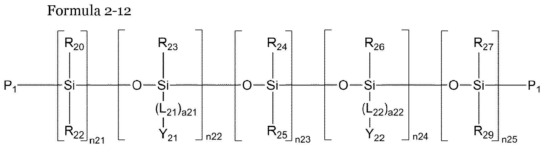


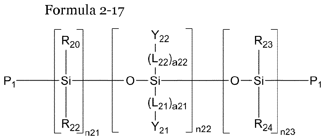
 Y11, Y12, Y21, and Y22 are each independently selected from a substituted or unsubstituted C6-C60 aryl group, a substituted or unsubstituted C6-C60 aryloxy group, and a substituted or unsubstituted C6-C60 arylthio group;L11, L12, L21, and L22 are each independently selected from a substituted or unsubstituted C1-C10 alkylene group and a substituted or unsubstituted C2-C10 alkenylene group;a11, a12, a21, and a22 are each independently selected from 0, 1, and 2;R10 to R19 and R20 to R29 are each independently selected from hydrogen, deuterium, a substituted or unsubstituted C1-C10 alkyl group, and a substituted or unsubstituted C3-C10 cycloalkyl group;P1 is a group represented by one of the following Formulae 6-1 to 6-3;
 L61 is selected from a substituted or unsubstituted C1-C10 alkylene group and a substituted or unsubstituted C2-C10 alkenylene group;a61 is selected from 0, 1, 2, and 3;R61 to R63 are each independently selected from hydrogen, a substituted or unsubstituted C1-C10 alkyl group, and a substituted or unsubstituted C1-C10 alkoxy group;* is a binding site with an adjacent atom;n11 to n15 and n21 to n25 are each independently selected from 0, 1, 2, 3, 4, and 5;a sum of n12 and n14 is 1 or 2; anda sum of n22 and n24 is 1 or 2.
 - The composition for fabricating an organic film as claimed in claim 1, wherein the first compound is one of the following Compounds 101 to 106:

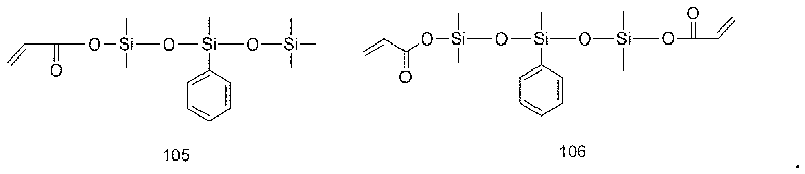
- The composition for fabricating an organic film as claimed in any preceding claim 1, further comprising a second compound, wherein:OP of the composition for fabricating an organic film is equal to or greater than 2.8 and equal to or less than 4.8; OP being (n1•OP1 + n2•OP2);RP of the composition for fabricating an organic film is equal to or greater than 0.01 and equal to or less than 0.46; RP being n1•RP1;n1 is (number of moles of the first compound)/(number of moles of the first compound + number of moles of the second compound);n2 is (number of moles of the second compound)/(number of moles of the first compound + number of moles of the second compound);OP1 is (total number of atoms of the first compound) / {(number of carbon atoms of the first compound) - (number of oxygen atoms of the first compound)};RP1 is {(number of carbon atoms of the substituent Y) X n} / (number of carbon atoms of the first compound); andOP2 is (total number of atoms of the second compound) / {(number of carbon atoms of the second compound) - (number of oxygen atoms of the second compound)}.
- The composition for fabricating an organic film as claimed in any preceding claim , further comprising an initiator.
- The composition for fabricating an organic film as claimed in any preceding claim , wherein the viscosity of the composition is (1 cps) 0.001 Pa s to (100 cps) 0.1 Pa s at 25 °C.
- Use of a composition for fabricating an organic film as claimed in any preceding claim in an organic light-emitting display apparatus, comprising:a substrate;an organic light-emitting device on the substrate; andan encapsulation layer on the organic light-emitting device;wherein the encapsulation layer includes 1, 2, or 3 sealing units, each sealing unit including the organic film and an inorganic film that are sequentially stacked on the organic light-emitting device; andthe organic film including a polymer prepared from the composition.as claimed in claim 1.
- Use of the composition as claimed in claim 12, wherein:the composition for fabricating an organic film further includes a second compound,OP of the composition for fabricating an organic film is equal to or greater than 2.8 and equal to or less than 4.8, OP being (n1•OP1 + n2•OP2);RP of the composition for fabricating an organic film is equal to or greater than 0.01 and equal to or less than 0.46, RP being n1•RP1;n1 is (number of moles of the first compound)/(number of moles of the first compound + number of moles of the second compound);n2 is (number of moles of the second compound)/(number of moles of the first compound + number of moles of the second compound);OP1 is (total number of atoms of the first compound) / {(number of carbon atoms of the first compound) - (number of oxygen atoms of the first compound)};RP1 is {(number of carbon atoms of the substituent Y) X n} / (number of carbon atoms of the first compound); andOP2 is (total number of atoms of the second compound) / {(number of carbon atoms of the second compound) - (number of oxygen atoms of the second compound)}.
- Use of the composition as claimed in claim 12 or claim 13, wherein the inorganic film includes at least one selected from metal, metal nitride, metal oxide, metal oxynitride, silicon nitride, silicon oxide, and silicon oxynitride.
- Use of the composition as claimed in any of claims 12 to 14, wherein the encapsulation layer further includes a lower inorganic film interposed between the organic light-emitting device and the organic film and/or the apparatus
further comprises at least one selected from a capping layer and a protective layer interposed between the organic light-emitting device and the encapsulation layer. - A method of manufacturing an organic light-emitting display apparatus, the method comprising:forming an organic light-emitting device on a substrate; andforming an encapsulation layer that includes 1, 2, or 3 sealing units, each of the sealing units including an organic film and an inorganic film that are sequentially stacked on the organic light-emitting device,wherein:forming the encapsulation layer includes forming the organic film by applying a composition for fabricating an organic film to a region where the organic film is to be formed and polymerizing the composition, the composition including a first compound;the first compound includes n substituents Y and m polymerizable groups P1;n is selected from 1, 2, 3, and 4;m is selected from 1, 2, 3, and 4;OP1 of the first compound is equal to or greater than 2.8 and equal to or less than 4.8; OP1 being (total number of atoms of the first compound) / {(number of carbon atoms of the first compound) - (number of oxygen atoms of the first compound)}; andRP1 of the first compound is equal to or greater than 0.01 and equal to or less than 0.46; RP1 being {(number of carbon atoms of the substituent Y) X n} / (number of carbon atoms of the first compound).
Applications Claiming Priority (1)
| Application Number | Priority Date | Filing Date | Title |
|---|---|---|---|
| KR1020140161624A KR102339283B1 (en) | 2014-11-19 | 2014-11-19 | Composition for fabricating organic film, organic light-emitting display apparatus manufactured by the same, and method for manufacturing the same |
Publications (2)
| Publication Number | Publication Date |
|---|---|
| EP3023444A1 true EP3023444A1 (en) | 2016-05-25 |
| EP3023444B1 EP3023444B1 (en) | 2019-03-13 |
Family
ID=54364962
Family Applications (1)
| Application Number | Title | Priority Date | Filing Date |
|---|---|---|---|
| EP15182794.6A Active EP3023444B1 (en) | 2014-11-19 | 2015-08-27 | Composition for fabricating organic film, organic light-emitting display apparatus manufactured using the same, and method of manufacturing the organic light-emitting display apparatus |
Country Status (5)
| Country | Link |
|---|---|
| US (1) | US9879035B2 (en) |
| EP (1) | EP3023444B1 (en) |
| KR (1) | KR102339283B1 (en) |
| CN (1) | CN105601810B (en) |
| TW (1) | TWI680963B (en) |
Cited By (1)
| Publication number | Priority date | Publication date | Assignee | Title |
|---|---|---|---|---|
| CN115851046A (en) * | 2023-03-01 | 2023-03-28 | 青州金昊新材料有限公司 | Paper-plastic model waterproof agent and preparation method and application thereof |
Families Citing this family (11)
| Publication number | Priority date | Publication date | Assignee | Title |
|---|---|---|---|---|
| JP6624808B2 (en) * | 2014-07-25 | 2019-12-25 | キヤノン株式会社 | Photocurable composition, method for producing cured product pattern using the same, method for producing optical component, method for producing circuit board |
| WO2017070889A1 (en) * | 2015-10-29 | 2017-05-04 | Boe Technology Group Co., Ltd. | Display device and fabrication method thereof |
| JP2017152256A (en) * | 2016-02-25 | 2017-08-31 | 株式会社ジャパンディスプレイ | Display device |
| KR20180033352A (en) * | 2016-09-23 | 2018-04-03 | 삼성디스플레이 주식회사 | Organic light emitting diode display compring capping layer |
| JP7042598B2 (en) * | 2016-12-14 | 2022-03-28 | 住友化学株式会社 | Method for manufacturing resin, resist composition and resist pattern |
| CN107104199A (en) * | 2017-04-19 | 2017-08-29 | 武汉华星光电技术有限公司 | Display panel and its manufacture method |
| WO2019047126A1 (en) * | 2017-09-07 | 2019-03-14 | 华为技术有限公司 | Organic light-emitting display (oled) screen and terminal |
| WO2019178782A1 (en) * | 2018-03-21 | 2019-09-26 | 华为技术有限公司 | Display screen and preparation method therefor, and mobile terminal |
| CN109343743A (en) * | 2018-12-07 | 2019-02-15 | 武汉华星光电半导体显示技术有限公司 | Flexible touch display module |
| CN110061149B (en) * | 2019-04-28 | 2020-11-10 | 福州大学 | A thin-film encapsulation method for flexible OLED devices |
| CN113135952B (en) * | 2021-04-01 | 2022-06-17 | 吉林奥来德光电材料股份有限公司 | A kind of photocurable monomer, photocurable composition, encapsulation film and display device |
Citations (3)
| Publication number | Priority date | Publication date | Assignee | Title |
|---|---|---|---|---|
| US20140070195A1 (en) * | 2012-09-12 | 2014-03-13 | Samsung Display Co., Ltd. | Organic light emitting device and method for preparing the same |
| EP2708580A1 (en) * | 2012-09-12 | 2014-03-19 | Basf Se | Photo-reactive polymer |
| US20140145154A1 (en) * | 2012-11-23 | 2014-05-29 | Samsung Display Co., Ltd. | Organic light-emitting device |
Family Cites Families (9)
| Publication number | Priority date | Publication date | Assignee | Title |
|---|---|---|---|---|
| US20030203210A1 (en) | 2002-04-30 | 2003-10-30 | Vitex Systems, Inc. | Barrier coatings and methods of making same |
| US20080006819A1 (en) | 2006-06-19 | 2008-01-10 | 3M Innovative Properties Company | Moisture barrier coatings for organic light emitting diode devices |
| US8222360B2 (en) * | 2009-02-13 | 2012-07-17 | Visiogen, Inc. | Copolymers for intraocular lens systems |
| KR101693367B1 (en) * | 2009-09-02 | 2017-01-06 | 삼성디스플레이 주식회사 | Organic layer composition and Liquid crystal display with the same |
| KR101255537B1 (en) | 2010-11-26 | 2013-04-16 | 삼성디스플레이 주식회사 | Flat display device and the manufacturing method thereof |
| KR20120065049A (en) | 2010-12-10 | 2012-06-20 | 삼성모바일디스플레이주식회사 | Organic light emitting diode display apparatus and manufacturing method thereof |
| KR101842586B1 (en) | 2011-04-05 | 2018-03-28 | 삼성디스플레이 주식회사 | Organic light emitting diode display and manufacturing method thereof |
| KR20140008215A (en) | 2012-07-11 | 2014-01-21 | 삼성디스플레이 주식회사 | Organic light-emitting display apparatus and manufacturing method thereof |
| KR101970361B1 (en) | 2012-08-20 | 2019-04-19 | 삼성디스플레이 주식회사 | Organic light emitting diode device and manufacturing method thereof |
-
2014
- 2014-11-19 KR KR1020140161624A patent/KR102339283B1/en active Active
-
2015
- 2015-05-08 US US14/707,750 patent/US9879035B2/en active Active
- 2015-08-21 TW TW104127248A patent/TWI680963B/en active
- 2015-08-27 EP EP15182794.6A patent/EP3023444B1/en active Active
- 2015-10-19 CN CN201510679760.4A patent/CN105601810B/en active Active
Patent Citations (3)
| Publication number | Priority date | Publication date | Assignee | Title |
|---|---|---|---|---|
| US20140070195A1 (en) * | 2012-09-12 | 2014-03-13 | Samsung Display Co., Ltd. | Organic light emitting device and method for preparing the same |
| EP2708580A1 (en) * | 2012-09-12 | 2014-03-19 | Basf Se | Photo-reactive polymer |
| US20140145154A1 (en) * | 2012-11-23 | 2014-05-29 | Samsung Display Co., Ltd. | Organic light-emitting device |
Cited By (1)
| Publication number | Priority date | Publication date | Assignee | Title |
|---|---|---|---|---|
| CN115851046A (en) * | 2023-03-01 | 2023-03-28 | 青州金昊新材料有限公司 | Paper-plastic model waterproof agent and preparation method and application thereof |
Also Published As
| Publication number | Publication date |
|---|---|
| TWI680963B (en) | 2020-01-01 |
| US9879035B2 (en) | 2018-01-30 |
| TW201619121A (en) | 2016-06-01 |
| CN105601810A (en) | 2016-05-25 |
| KR102339283B1 (en) | 2021-12-15 |
| KR20160060211A (en) | 2016-05-30 |
| EP3023444B1 (en) | 2019-03-13 |
| US20160137769A1 (en) | 2016-05-19 |
| CN105601810B (en) | 2020-09-04 |
Similar Documents
| Publication | Publication Date | Title |
|---|---|---|
| EP3023444B1 (en) | Composition for fabricating organic film, organic light-emitting display apparatus manufactured using the same, and method of manufacturing the organic light-emitting display apparatus | |
| KR102072799B1 (en) | Organic light emitting device and method for preparing the same | |
| CN107851730B (en) | Organic light emitting display | |
| KR101943689B1 (en) | Organic light emmiting diode display apparatus | |
| KR101943688B1 (en) | Organic light emmiting diode display apparatus | |
| CN107075033A (en) | Constituent for display seal material, the organic protection layer containing it, contain its display equipment | |
| KR102736353B1 (en) | An organic film forming composition and electronic apparatus comprising a cured product thereof | |
| JP7736004B2 (en) | Composition for sealing electronic devices, method for forming sealing film for electronic devices, and sealing film for electronic devices | |
| TWI759752B (en) | Composition for encapsulating organic light emitting diode device and display device | |
| JP2015103389A (en) | Organic el device | |
| KR20180102038A (en) | Photo-curable composition, organic protective layer comprising the same, and apparatus comprising the same | |
| JP7786457B2 (en) | Composition for sealing electronic devices, method for forming sealing film for electronic devices, and sealing film for electronic devices | |
| JP7762514B2 (en) | Composition for sealing organic light-emitting device and organic light-emitting display device including organic layer produced therefrom | |
| KR20240009473A (en) | Composition for electronic device encapsulation, method of forming electronic device encapsulation film, and electronic device encapsulation film | |
| KR20170115118A (en) | Composition and compound for encapsulating organic light emitting diode and oencapsulated apparatus comprising the same | |
| KR20250027790A (en) | Composition for electronic device encapsulation, electronic device encapsulation film and method for forming electronic device encapsulation film |
Legal Events
| Date | Code | Title | Description |
|---|---|---|---|
| AK | Designated contracting states |
Kind code of ref document: A1 Designated state(s): AL AT BE BG CH CY CZ DE DK EE ES FI FR GB GR HR HU IE IS IT LI LT LU LV MC MK MT NL NO PL PT RO RS SE SI SK SM TR |
|
| AX | Request for extension of the european patent |
Extension state: BA ME |
|
| PUAI | Public reference made under article 153(3) epc to a published international application that has entered the european phase |
Free format text: ORIGINAL CODE: 0009012 |
|
| STAA | Information on the status of an ep patent application or granted ep patent |
Free format text: STATUS: REQUEST FOR EXAMINATION WAS MADE |
|
| 17P | Request for examination filed |
Effective date: 20161124 |
|
| RBV | Designated contracting states (corrected) |
Designated state(s): AL AT BE BG CH CY CZ DE DK EE ES FI FR GB GR HR HU IE IS IT LI LT LU LV MC MK MT NL NO PL PT RO RS SE SI SK SM TR |
|
| REG | Reference to a national code |
Ref country code: DE Ref legal event code: R079 Ref document number: 602015026203 Country of ref document: DE Free format text: PREVIOUS MAIN CLASS: C08F0222100000 Ipc: C09D0133080000 |
|
| RIC1 | Information provided on ipc code assigned before grant |
Ipc: C09D 133/10 20060101ALI20180727BHEP Ipc: H01L 51/52 20060101ALI20180727BHEP Ipc: C08F 230/08 20060101ALN20180727BHEP Ipc: C08F 222/10 20060101ALN20180727BHEP Ipc: C09D 133/08 20060101AFI20180727BHEP Ipc: C09D 4/00 20060101ALI20180727BHEP |
|
| GRAP | Despatch of communication of intention to grant a patent |
Free format text: ORIGINAL CODE: EPIDOSNIGR1 |
|
| STAA | Information on the status of an ep patent application or granted ep patent |
Free format text: STATUS: GRANT OF PATENT IS INTENDED |
|
| RIC1 | Information provided on ipc code assigned before grant |
Ipc: C08F 230/08 20060101ALN20180827BHEP Ipc: C09D 133/10 20060101ALI20180827BHEP Ipc: H01L 51/52 20060101ALI20180827BHEP Ipc: C09D 133/08 20060101AFI20180827BHEP Ipc: C08F 222/10 20060101ALN20180827BHEP Ipc: C09D 4/00 20060101ALI20180827BHEP |
|
| INTG | Intention to grant announced |
Effective date: 20180924 |
|
| GRAS | Grant fee paid |
Free format text: ORIGINAL CODE: EPIDOSNIGR3 |
|
| GRAA | (expected) grant |
Free format text: ORIGINAL CODE: 0009210 |
|
| STAA | Information on the status of an ep patent application or granted ep patent |
Free format text: STATUS: THE PATENT HAS BEEN GRANTED |
|
| AK | Designated contracting states |
Kind code of ref document: B1 Designated state(s): AL AT BE BG CH CY CZ DE DK EE ES FI FR GB GR HR HU IE IS IT LI LT LU LV MC MK MT NL NO PL PT RO RS SE SI SK SM TR |
|
| REG | Reference to a national code |
Ref country code: GB Ref legal event code: FG4D |
|
| REG | Reference to a national code |
Ref country code: CH Ref legal event code: EP Ref country code: AT Ref legal event code: REF Ref document number: 1107625 Country of ref document: AT Kind code of ref document: T Effective date: 20190315 |
|
| REG | Reference to a national code |
Ref country code: IE Ref legal event code: FG4D |
|
| REG | Reference to a national code |
Ref country code: DE Ref legal event code: R096 Ref document number: 602015026203 Country of ref document: DE |
|
| REG | Reference to a national code |
Ref country code: NL Ref legal event code: MP Effective date: 20190313 |
|
| REG | Reference to a national code |
Ref country code: LT Ref legal event code: MG4D |
|
| PG25 | Lapsed in a contracting state [announced via postgrant information from national office to epo] |
Ref country code: NO Free format text: LAPSE BECAUSE OF FAILURE TO SUBMIT A TRANSLATION OF THE DESCRIPTION OR TO PAY THE FEE WITHIN THE PRESCRIBED TIME-LIMIT Effective date: 20190613 Ref country code: FI Free format text: LAPSE BECAUSE OF FAILURE TO SUBMIT A TRANSLATION OF THE DESCRIPTION OR TO PAY THE FEE WITHIN THE PRESCRIBED TIME-LIMIT Effective date: 20190313 Ref country code: SE Free format text: LAPSE BECAUSE OF FAILURE TO SUBMIT A TRANSLATION OF THE DESCRIPTION OR TO PAY THE FEE WITHIN THE PRESCRIBED TIME-LIMIT Effective date: 20190313 Ref country code: LT Free format text: LAPSE BECAUSE OF FAILURE TO SUBMIT A TRANSLATION OF THE DESCRIPTION OR TO PAY THE FEE WITHIN THE PRESCRIBED TIME-LIMIT Effective date: 20190313 |
|
| PG25 | Lapsed in a contracting state [announced via postgrant information from national office to epo] |
Ref country code: NL Free format text: LAPSE BECAUSE OF FAILURE TO SUBMIT A TRANSLATION OF THE DESCRIPTION OR TO PAY THE FEE WITHIN THE PRESCRIBED TIME-LIMIT Effective date: 20190313 Ref country code: LV Free format text: LAPSE BECAUSE OF FAILURE TO SUBMIT A TRANSLATION OF THE DESCRIPTION OR TO PAY THE FEE WITHIN THE PRESCRIBED TIME-LIMIT Effective date: 20190313 Ref country code: HR Free format text: LAPSE BECAUSE OF FAILURE TO SUBMIT A TRANSLATION OF THE DESCRIPTION OR TO PAY THE FEE WITHIN THE PRESCRIBED TIME-LIMIT Effective date: 20190313 Ref country code: GR Free format text: LAPSE BECAUSE OF FAILURE TO SUBMIT A TRANSLATION OF THE DESCRIPTION OR TO PAY THE FEE WITHIN THE PRESCRIBED TIME-LIMIT Effective date: 20190614 Ref country code: BG Free format text: LAPSE BECAUSE OF FAILURE TO SUBMIT A TRANSLATION OF THE DESCRIPTION OR TO PAY THE FEE WITHIN THE PRESCRIBED TIME-LIMIT Effective date: 20190613 Ref country code: RS Free format text: LAPSE BECAUSE OF FAILURE TO SUBMIT A TRANSLATION OF THE DESCRIPTION OR TO PAY THE FEE WITHIN THE PRESCRIBED TIME-LIMIT Effective date: 20190313 |
|
| REG | Reference to a national code |
Ref country code: AT Ref legal event code: MK05 Ref document number: 1107625 Country of ref document: AT Kind code of ref document: T Effective date: 20190313 |
|
| PG25 | Lapsed in a contracting state [announced via postgrant information from national office to epo] |
Ref country code: IT Free format text: LAPSE BECAUSE OF FAILURE TO SUBMIT A TRANSLATION OF THE DESCRIPTION OR TO PAY THE FEE WITHIN THE PRESCRIBED TIME-LIMIT Effective date: 20190313 Ref country code: EE Free format text: LAPSE BECAUSE OF FAILURE TO SUBMIT A TRANSLATION OF THE DESCRIPTION OR TO PAY THE FEE WITHIN THE PRESCRIBED TIME-LIMIT Effective date: 20190313 Ref country code: RO Free format text: LAPSE BECAUSE OF FAILURE TO SUBMIT A TRANSLATION OF THE DESCRIPTION OR TO PAY THE FEE WITHIN THE PRESCRIBED TIME-LIMIT Effective date: 20190313 Ref country code: AL Free format text: LAPSE BECAUSE OF FAILURE TO SUBMIT A TRANSLATION OF THE DESCRIPTION OR TO PAY THE FEE WITHIN THE PRESCRIBED TIME-LIMIT Effective date: 20190313 Ref country code: CZ Free format text: LAPSE BECAUSE OF FAILURE TO SUBMIT A TRANSLATION OF THE DESCRIPTION OR TO PAY THE FEE WITHIN THE PRESCRIBED TIME-LIMIT Effective date: 20190313 Ref country code: ES Free format text: LAPSE BECAUSE OF FAILURE TO SUBMIT A TRANSLATION OF THE DESCRIPTION OR TO PAY THE FEE WITHIN THE PRESCRIBED TIME-LIMIT Effective date: 20190313 Ref country code: SK Free format text: LAPSE BECAUSE OF FAILURE TO SUBMIT A TRANSLATION OF THE DESCRIPTION OR TO PAY THE FEE WITHIN THE PRESCRIBED TIME-LIMIT Effective date: 20190313 Ref country code: PT Free format text: LAPSE BECAUSE OF FAILURE TO SUBMIT A TRANSLATION OF THE DESCRIPTION OR TO PAY THE FEE WITHIN THE PRESCRIBED TIME-LIMIT Effective date: 20190713 |
|
| PG25 | Lapsed in a contracting state [announced via postgrant information from national office to epo] |
Ref country code: PL Free format text: LAPSE BECAUSE OF FAILURE TO SUBMIT A TRANSLATION OF THE DESCRIPTION OR TO PAY THE FEE WITHIN THE PRESCRIBED TIME-LIMIT Effective date: 20190313 Ref country code: SM Free format text: LAPSE BECAUSE OF FAILURE TO SUBMIT A TRANSLATION OF THE DESCRIPTION OR TO PAY THE FEE WITHIN THE PRESCRIBED TIME-LIMIT Effective date: 20190313 |
|
| REG | Reference to a national code |
Ref country code: DE Ref legal event code: R097 Ref document number: 602015026203 Country of ref document: DE |
|
| PG25 | Lapsed in a contracting state [announced via postgrant information from national office to epo] |
Ref country code: AT Free format text: LAPSE BECAUSE OF FAILURE TO SUBMIT A TRANSLATION OF THE DESCRIPTION OR TO PAY THE FEE WITHIN THE PRESCRIBED TIME-LIMIT Effective date: 20190313 Ref country code: IS Free format text: LAPSE BECAUSE OF FAILURE TO SUBMIT A TRANSLATION OF THE DESCRIPTION OR TO PAY THE FEE WITHIN THE PRESCRIBED TIME-LIMIT Effective date: 20190713 |
|
| PLBE | No opposition filed within time limit |
Free format text: ORIGINAL CODE: 0009261 |
|
| STAA | Information on the status of an ep patent application or granted ep patent |
Free format text: STATUS: NO OPPOSITION FILED WITHIN TIME LIMIT |
|
| PG25 | Lapsed in a contracting state [announced via postgrant information from national office to epo] |
Ref country code: DK Free format text: LAPSE BECAUSE OF FAILURE TO SUBMIT A TRANSLATION OF THE DESCRIPTION OR TO PAY THE FEE WITHIN THE PRESCRIBED TIME-LIMIT Effective date: 20190313 |
|
| 26N | No opposition filed |
Effective date: 20191216 |
|
| PG25 | Lapsed in a contracting state [announced via postgrant information from national office to epo] |
Ref country code: SI Free format text: LAPSE BECAUSE OF FAILURE TO SUBMIT A TRANSLATION OF THE DESCRIPTION OR TO PAY THE FEE WITHIN THE PRESCRIBED TIME-LIMIT Effective date: 20190313 |
|
| PG25 | Lapsed in a contracting state [announced via postgrant information from national office to epo] |
Ref country code: TR Free format text: LAPSE BECAUSE OF FAILURE TO SUBMIT A TRANSLATION OF THE DESCRIPTION OR TO PAY THE FEE WITHIN THE PRESCRIBED TIME-LIMIT Effective date: 20190313 |
|
| PG25 | Lapsed in a contracting state [announced via postgrant information from national office to epo] |
Ref country code: MC Free format text: LAPSE BECAUSE OF FAILURE TO SUBMIT A TRANSLATION OF THE DESCRIPTION OR TO PAY THE FEE WITHIN THE PRESCRIBED TIME-LIMIT Effective date: 20190313 Ref country code: LU Free format text: LAPSE BECAUSE OF NON-PAYMENT OF DUE FEES Effective date: 20190827 Ref country code: CH Free format text: LAPSE BECAUSE OF NON-PAYMENT OF DUE FEES Effective date: 20190831 Ref country code: LI Free format text: LAPSE BECAUSE OF NON-PAYMENT OF DUE FEES Effective date: 20190831 |
|
| REG | Reference to a national code |
Ref country code: BE Ref legal event code: MM Effective date: 20190831 |
|
| PG25 | Lapsed in a contracting state [announced via postgrant information from national office to epo] |
Ref country code: IE Free format text: LAPSE BECAUSE OF NON-PAYMENT OF DUE FEES Effective date: 20190827 Ref country code: FR Free format text: LAPSE BECAUSE OF NON-PAYMENT OF DUE FEES Effective date: 20190831 |
|
| PG25 | Lapsed in a contracting state [announced via postgrant information from national office to epo] |
Ref country code: BE Free format text: LAPSE BECAUSE OF NON-PAYMENT OF DUE FEES Effective date: 20190831 |
|
| PG25 | Lapsed in a contracting state [announced via postgrant information from national office to epo] |
Ref country code: CY Free format text: LAPSE BECAUSE OF FAILURE TO SUBMIT A TRANSLATION OF THE DESCRIPTION OR TO PAY THE FEE WITHIN THE PRESCRIBED TIME-LIMIT Effective date: 20190313 |
|
| PG25 | Lapsed in a contracting state [announced via postgrant information from national office to epo] |
Ref country code: MT Free format text: LAPSE BECAUSE OF FAILURE TO SUBMIT A TRANSLATION OF THE DESCRIPTION OR TO PAY THE FEE WITHIN THE PRESCRIBED TIME-LIMIT Effective date: 20190313 Ref country code: HU Free format text: LAPSE BECAUSE OF FAILURE TO SUBMIT A TRANSLATION OF THE DESCRIPTION OR TO PAY THE FEE WITHIN THE PRESCRIBED TIME-LIMIT; INVALID AB INITIO Effective date: 20150827 |
|
| PG25 | Lapsed in a contracting state [announced via postgrant information from national office to epo] |
Ref country code: MK Free format text: LAPSE BECAUSE OF FAILURE TO SUBMIT A TRANSLATION OF THE DESCRIPTION OR TO PAY THE FEE WITHIN THE PRESCRIBED TIME-LIMIT Effective date: 20190313 |
|
| P01 | Opt-out of the competence of the unified patent court (upc) registered |
Effective date: 20230515 |
|
| PGFP | Annual fee paid to national office [announced via postgrant information from national office to epo] |
Ref country code: DE Payment date: 20250721 Year of fee payment: 11 |
|
| PGFP | Annual fee paid to national office [announced via postgrant information from national office to epo] |
Ref country code: GB Payment date: 20250722 Year of fee payment: 11 |