EP3021176B1 - Low power bipolar 360 degrees time to digital converter - Google Patents
Low power bipolar 360 degrees time to digital converter Download PDFInfo
- Publication number
- EP3021176B1 EP3021176B1 EP15190054.5A EP15190054A EP3021176B1 EP 3021176 B1 EP3021176 B1 EP 3021176B1 EP 15190054 A EP15190054 A EP 15190054A EP 3021176 B1 EP3021176 B1 EP 3021176B1
- Authority
- EP
- European Patent Office
- Prior art keywords
- delay
- edge
- signal
- time
- delay line
- Prior art date
- Legal status (The legal status is an assumption and is not a legal conclusion. Google has not performed a legal analysis and makes no representation as to the accuracy of the status listed.)
- Active
Links
- 238000005259 measurement Methods 0.000 claims description 88
- 238000004364 calculation method Methods 0.000 claims description 49
- 238000013139 quantization Methods 0.000 claims description 31
- 238000000034 method Methods 0.000 claims description 30
- 238000006243 chemical reaction Methods 0.000 claims description 21
- 238000012545 processing Methods 0.000 claims description 4
- 230000006870 function Effects 0.000 description 30
- 230000000630 rising effect Effects 0.000 description 20
- 241000238876 Acari Species 0.000 description 17
- 238000004891 communication Methods 0.000 description 10
- 230000004087 circulation Effects 0.000 description 9
- 238000010295 mobile communication Methods 0.000 description 9
- 238000005516 engineering process Methods 0.000 description 8
- 230000010355 oscillation Effects 0.000 description 7
- 102000017177 Fibromodulin Human genes 0.000 description 5
- 108010013996 Fibromodulin Proteins 0.000 description 5
- 230000008901 benefit Effects 0.000 description 4
- 238000004590 computer program Methods 0.000 description 4
- 230000003287 optical effect Effects 0.000 description 4
- 230000008569 process Effects 0.000 description 4
- 230000001902 propagating effect Effects 0.000 description 4
- 230000009471 action Effects 0.000 description 3
- 230000008859 change Effects 0.000 description 3
- 230000004044 response Effects 0.000 description 3
- 230000001360 synchronised effect Effects 0.000 description 3
- 238000004422 calculation algorithm Methods 0.000 description 2
- 230000001934 delay Effects 0.000 description 2
- 238000010586 diagram Methods 0.000 description 2
- 239000000835 fiber Substances 0.000 description 2
- 238000002347 injection Methods 0.000 description 2
- 239000007924 injection Substances 0.000 description 2
- 238000003780 insertion Methods 0.000 description 2
- 230000037431 insertion Effects 0.000 description 2
- 238000004519 manufacturing process Methods 0.000 description 2
- 230000008520 organization Effects 0.000 description 2
- 230000009467 reduction Effects 0.000 description 2
- 230000002441 reversible effect Effects 0.000 description 2
- 230000007704 transition Effects 0.000 description 2
- 230000000712 assembly Effects 0.000 description 1
- 238000000429 assembly Methods 0.000 description 1
- 230000000295 complement effect Effects 0.000 description 1
- 230000003247 decreasing effect Effects 0.000 description 1
- 230000007812 deficiency Effects 0.000 description 1
- 230000000593 degrading effect Effects 0.000 description 1
- 230000003111 delayed effect Effects 0.000 description 1
- 230000001419 dependent effect Effects 0.000 description 1
- XPYGGHVSFMUHLH-UUSULHAXSA-N falecalcitriol Chemical compound C1(/[C@@H]2CC[C@@H]([C@]2(CCC1)C)[C@@H](CCCC(O)(C(F)(F)F)C(F)(F)F)C)=C\C=C1\C[C@@H](O)C[C@H](O)C1=C XPYGGHVSFMUHLH-UUSULHAXSA-N 0.000 description 1
- RVRCFVVLDHTFFA-UHFFFAOYSA-N heptasodium;tungsten;nonatriacontahydrate Chemical compound O.O.O.O.O.O.O.O.O.O.O.O.O.O.O.O.O.O.O.O.O.O.O.O.O.O.O.O.O.O.O.O.O.O.O.O.O.O.O.[Na+].[Na+].[Na+].[Na+].[Na+].[Na+].[Na+].[W].[W].[W].[W].[W].[W].[W].[W].[W].[W].[W] RVRCFVVLDHTFFA-UHFFFAOYSA-N 0.000 description 1
- 230000000977 initiatory effect Effects 0.000 description 1
- 229940052961 longrange Drugs 0.000 description 1
- 230000007774 longterm Effects 0.000 description 1
- 238000013507 mapping Methods 0.000 description 1
- 238000000691 measurement method Methods 0.000 description 1
- 230000010363 phase shift Effects 0.000 description 1
- 230000000644 propagated effect Effects 0.000 description 1
- 238000001228 spectrum Methods 0.000 description 1
- 238000012546 transfer Methods 0.000 description 1
- 230000007723 transport mechanism Effects 0.000 description 1
Images


Classifications
-
- G—PHYSICS
- G04—HOROLOGY
- G04F—TIME-INTERVAL MEASURING
- G04F10/00—Apparatus for measuring unknown time intervals by electric means
- G04F10/005—Time-to-digital converters [TDC]
-
- H—ELECTRICITY
- H03—ELECTRONIC CIRCUITRY
- H03L—AUTOMATIC CONTROL, STARTING, SYNCHRONISATION, OR STABILISATION OF GENERATORS OF ELECTRONIC OSCILLATIONS OR PULSES
- H03L7/00—Automatic control of frequency or phase; Synchronisation
- H03L7/06—Automatic control of frequency or phase; Synchronisation using a reference signal applied to a frequency- or phase-locked loop
- H03L7/08—Details of the phase-locked loop
- H03L7/099—Details of the phase-locked loop concerning mainly the controlled oscillator of the loop
- H03L7/0991—Details of the phase-locked loop concerning mainly the controlled oscillator of the loop the oscillator being a digital oscillator, e.g. composed of a fixed oscillator followed by a variable frequency divider
-
- H—ELECTRICITY
- H03—ELECTRONIC CIRCUITRY
- H03M—CODING; DECODING; CODE CONVERSION IN GENERAL
- H03M1/00—Analogue/digital conversion; Digital/analogue conversion
- H03M1/002—Provisions or arrangements for saving power, e.g. by allowing a sleep mode, using lower supply voltage for downstream stages, using multiple clock domains or by selectively turning on stages when needed
-
- H—ELECTRICITY
- H03—ELECTRONIC CIRCUITRY
- H03M—CODING; DECODING; CODE CONVERSION IN GENERAL
- H03M1/00—Analogue/digital conversion; Digital/analogue conversion
- H03M1/06—Continuously compensating for, or preventing, undesired influence of physical parameters
- H03M1/08—Continuously compensating for, or preventing, undesired influence of physical parameters of noise
- H03M1/0836—Continuously compensating for, or preventing, undesired influence of physical parameters of noise of phase error, e.g. jitter
Definitions
- Phase-locked loops can provide precise generation and alignment of timing for a wide variety of applications.
- Digital phase-locked loops DPLLs
- TDCs time to digital converters
- ADPLLs digital phase locked loops
- TDCs typically measure positive times
- an additional TDC offset is normally introduced in front of a digital loop filter of the ADPLL, in which the TDC offset is chosen to give a margin for a multi-modulus divider (MMD) induced edge variation.
- MMD multi-modulus divider
- Document US 2009/0219073 A1 describes a high resolution time-to-digital converter. Further, document US2014/0091866 A1 describes a ring oscillator and document WO 2007/093221 A1 describes a time-to-digital conversion with calibration pulse injection.
- a clock generating circuit includes: a counter that counts a number of pulses of an oscillation clock signal existed within one cycle of a reference clock signal; a first time-to-digital converter that generates a plurality of phases of first clock signals by delaying the oscillation clock signal; a second time-to-digital converter that generates a plurality of phases of second clock signals by delaying the oscillation clock signal by a short delay time; a third time-to-digital converter that generates a plurality of phases of third clock signals by delaying the delayed first clock signal; a delay control unit that outputs a delay control signal based on a difference between a cycle of the oscillation clock signal and a target cycle;; and an oscillator that generates, based on a cycle of the reference clock signal, the oscillation clock signal whose cycle is 1/m of the cycle of the reference clock signal.
- TDCs are disclosed, which avoid having to digitally introduce a TDC offset in front of the PLL loop filter by facilitating bipolar time measurement techniques.
- This TDC offset normally operates to counteract the capability of TDCs to measure positive time differences only.
- the TDC offsets can be eliminated by systems and methods provided herein, which can be implemented in various components and systems, such as frequency modulated ADPLLs applicable in polar-modulators.
- a digital oscillator (such as the oscillator of the DPLL employing the TDC) is utilized for determining a coarse time measurement/quantization that biases a phase locked loop before being locked in a frequency of operation (e.g., the reference frequency being synchronized to a feedback or divider frequency) by a fine tuning/timing measurement.
- a digital control oscillator calculation component is configured to calculate the coarse time measurement or a coarse tuning measurement from counted digital oscillator edges, even when the digital oscillator frequencies being received have been modulated (e.g., a polar frequency modulator or the like modulator).
- the low frequency part of a modulator e.g., fractional sample rate converter of the modulator can be used to calculate the coarse time measurements.
- An edge selector, a phase generator and a delay line can generate a bipolar time measurement (e.g., a sign value) for the fine tuning/timing measurement and generate a cancellation of an offset that depends on a process, a voltage or a temperature variance with respect to use, time or change of the system.
- a bipolar time measurement e.g., a sign value
- systems disclosed herein can operate as a bipolar time measuring single TDC with a single delay line that also facilitates a generation of bipolar time measurements, which indicate or represent different polarities based on a timing of a reception of a received reference signal edge or a received feedback/divider signal edge.
- the systems disclosed can determine the bipolar time measurement with modulated frequencies. Additional aspects and details of the disclosure are further described below with reference to the figures.
- the mobile communication device 100 comprises a digital baseband processor 102, an RF frontend 104 and an antenna port 108 for connecting to an antenna 106.
- the mobile communication device 100 can comprise an exemplary TDC 110 as part of the digital baseband processor 102 or the RF frontend 104, which can also operate as a component within a DPLL for example. Nevertheless, it is also possible that each of the digital baseband processor 102 and the RF frontend 104 comprises such a TDC 110 or even comprises more than one of such TDC 110.
- the RF frontend 104 is coupled to the digital baseband processor 102 and the antenna port 108.
- the TDC 110 can operate with a differential delay component that ensures there is no delay mismatch between a positive and negative input and output of the differential delay chain.
- the digital controlled oscillator (DCO) circulation counter can be used to determine a coarse time quantization or a coarse time measurement for coarse tuning without use of additional multiplexers for propagation or circulation counting. These advantages lead to a better phase noise performance, a symmetrical clock generation and a reduction in quantization noise.
- the quantization noise can be reduced when the TDC 110 is used with a differential delay line of the mobile communication device 100, which can operate to replace circulation or propagation counting by using the DCO for determining coarse time quantization.
- the coarse quantization time can be calculated by the sum of the DCO periods of the DCO.
- the TDC 110 achieves a resolution enhancement, for example, when the TDC 110 is used for measuring time between certain events.
- the TDC 110 enables a more precise generation of clock signals in the mobile communication device 100 and a more precise measuring of time differences (such as in a DPLL).
- the improved generation of clock signals and improved measuring of time differences enables a reduction of a noise floor in the mobile communication device 100 and therefore improves or facilitates the overall performance of the mobile communication device 100.
- the TDC 200 comprises a differential delay line 202 that operates to propagate a signal edge via differential delay stages 204a to 204n to facilitate measuring of times between at least two edges of the same or different signals.
- the time difference representing a phase error between a reference signal and a feedback signal in a DPLL is measured by the TDC 200.
- a differential delay line is contemplated, a single ended delay could also be embodied as the delay line.
- the delay stages 204a to 204n each include a first delay element 206a to 206n and a second delay element 208a to 208n, which can represent one or more elements for each stage, such as for a differential chain of delay elements 206a to 206n or for 208a to 208n, for example.
- the first delay elements 206a to 206n can be connected in series to form a first positive delay chain (e.g., a positive delay chain) of the differential delay line 202.
- the second delay elements 208a to 208n can be connected in series to form a second negative delay chain (e.g., a negative delay chain) of the differential delay line 202.
- the delay elements of the differential delay line 202 can comprise differential delay elements with a positive and a negative delay line or path that can be cross coupled at a positive input and a negative input of each delay element, in which the differential delay elements of the chains are free, independent of or without any mismatch.
- each of the delays elements can be synchronized.
- the differential delay line 202 can comprise a first plurality of comparators 210a to 210n, inputs of which are connected to the outputs of the first delay elements 206a to 206n.
- the differential delay line 202 comprises a second plurality of comparators 212a to 212n and can be implemented to propagate signal edges without additional multiplexers.
- the differential delay line 202 comprises per delay stage an associated comparator 210a to 210n and 212a to 212n, a first input of which can be connected to an output of one of the delay elements of the associated delay stage 204a to 204n and a second input of which is connected to the other delay element of the associated delay stage 204a to 204n, as such each comparator can have a positive and negative input
- inputs of every second comparator may be complementarily connected to the outputs of the associated delay stage with the inputs of the comparators associated to the preceding delay stage.
- a first input of a first comparator could be connected to the output of the first delay element of the first delay stage and a second input of the first comparator would be connected to the output of the second delay element of the first delay stage.
- the first input of this comparator could be connected to the output of the second delay element of the preceding delay stage and the second input of the comparator would be connected to the output of the first delay element of the preceding delay stage.
- the differential delay line 202 is configured to measure time differences such as a time between the insertion of the start edge and the occurrence of a stop signal, in which the insertion of the start and stop edges can be done directly into the line from a phase generator 224 without utilizing or independently of a multiplexer between the phase generator and the differential delay line 202.
- a complementary circuiting of the inputs of the comparators or the outputs of the comparators being associated to directly succeeding delay stages, as discussed in the above example configurations, can facilitate a hot one decoder 214, 216 to determine the position of the start edge in the differential delay line 202.
- the TDC 200 comprises a top hot one decoder 214 and a bottom hot one decoder 216, a top thermo to binary decoder 218 and a bottom thermo to binary decoder 220.
- the TDC 200 utilizes a DCO circulation counting for coarse time quantization and initiating the start and stop edges to the delay line via the phase generator 224.
- the TDC 200 thus avoids power hungry and phase noise degrading ring oscillator circulations for coarse time quantization and avoids circulation determinations from a top and bottom counter.
- the differential implementation of the TDC 200 can be used, for example, for an all-digital wireless PLL (ADPLL).
- ADPLL all-digital wireless PLL
- the time to digital converter 200 can operate to measure the time between the rising edge of the 26 MHz reference clock and the rising edge of a divider edge such as a multi modulus divider (MMD) edge.
- MMD multi modulus divider
- An edge selector 222 provides a start signal and a stop signal to the phase generator 224, which, in turn, generates a start edge and a stop edge into the differential delay line 202 in response to receiving the start signal and the stop signal.
- the edge selector 222 is therefore configured to compare a reference signal of a reference clock (Ref clk) and a divider signal of a divider clock (Div_clk) and generate the start signal and the stop signal to a phase generator 224. Furthermore, the edge selector 222 generates a sign value (sign) to a coarse time calculation component (labelled T m_DCO calculation) 228, in which the sign value is based on an order of receiving the reference signal and the divider signal as a bipolar time measurement, as further detailed below.
- T m_DCO calculation coarse time calculation component
- the differential delay line 202 can comprise multiple different delay stages 204a to 204n with a unit delay, for example, of about 8 picoseconds or other delay.
- the differential delay line 202 comprises, for example, a sufficient number of delay elements to accommodate or handle a maximal DCO period divided by 2 or 4, for example, as represented by the division component 232.
- the start edge propagates at least partially through the differential delay stages 204a to 204n to an extent according to DCO edges of the DCO 230, such as a DCO rising edge or a DCO falling edge of the DCO 230.
- the polarity of the edge can change or reverse after each circulation or propagation through the differential delay line 202, which is also based on a rising or a falling DCO edge. In this manner, positive and negative determinations can come from a reuse of the same delay line that facilitates the offset cancelation.
- a bipolar measurement is generated from the edge selector block 222, which is discussed further below, for further determining a coarse time quantization.
- the stop edge or stop signal is derived from a next rising DCO edge.
- the stop signal denoted as Stop_Ticks 1 and Stop_Ticks 2 from the phase generator 224 results from the edge selector 222 and is a function of a next rising edge of the DCO 230.
- the Stop Ticks 1 and Stop Ticks 2 signals trigger the comparators 210a to 210n and 212a to 212n to latch current states of the delay stages, for example.
- the hot one decoder 214 and 216 are configured to convert the comparator output (as Comp_ticks1, Comp_ticks2) that represents the latched current state as a thermometer code in a circulation independent hot one code.
- the two thermo to binary decoders 218, 220 are configured to convert the top and bottom 16 hot one decoder outputs of the hot one decoder 214 and 216 to a binary code, such as a 4-bit binary code.
- the phase generator 224 of the TDC 200 controls the propagating and latching of the delay stages 204a to 204n via a propagation mode and a latching mode as a function of a start and stop signal provided by the edge selector 222 and a DCO edge of the DCO 230.
- a start signal 302 is initiated by the edge selector 222 to the phase generator 224.
- the phase generator 224 converts the start signal 302 into a start_p signal 306 and a start_n signal 308 as a positive start_p edge and a negative start_n edge, for example.
- the positive differential edge propagates (Ticks 1 316) along the differential delay line 202 at the conversion of the start signal 302 to a start delay line plus (start DL +) until the first subsequent rising DCO edge latches the Delay Line states with the comparators 210a to 210n (Tick1 comparators).
- the latching in a latch mode of the delay line 202 is initiated by first subsequent DCO edge after the positive start signal 306 initiates propagating, for example.
- a conversion result 402 of the comparator latching is denoted as Comp_tick1 402, as illustrated in FIG. 4 .
- the Hot One Decoder 214 converts the first Comp_tick1 402 (1 / 0) transition into a hot one code 404.
- the hot one code 404 is converted by the thermo to bin decoder 218 in a binary Ticks1 value of the Ticks 1 propagation 316, as illustrated in FIG. 3 .
- a rising stop edge 304 is received by the phase generator 224 from the edge selector 222.
- the phase generator 224 converts the stop signal 304 into a falling edge at the start signal 306 start_p and a rising edge at the start signal 308 start n.
- This second differential edge (conversion of stop signal 304) has an opposite direction in comparison to the first differential edge (conversion of start signal 302) and propagates along the differential delay line 202 as shown at Ticks2 318 until the next rising DCO edge 310 initiates subsequent to the stop signal 304 facilitates a stop_Ticks2 signal 314, which causes a latching mode of the delay line 202 that operates to latch the delay line 202 state with the comparators 212a to 212n respectively (denoted also as correspondingTicks2 comparators).
- the latch result, or the latched/locked state is denoted as a binary signal 406 in FIG. 4 or as Comp_ticks2.
- the hot one decoder 216 converts the first Comp_tick2 (1 / 0) transition into the binary code 406, a Hot one code 1.
- the hot one code 406 is then converted by the thermo to bin decoder 220 into a binary Ticks2 value of the opposing Ticks 2 propagation 318.
- the final time measurement (i.e., Result) can be represented as the final start/stop time t start stop , which is calculated as a function of t tm_DCO , t ticks1 , t ticks2 and ⁇ t, wherein ⁇ t is the delay of one unity delay element 204a of delay elements 204a to 204n, or 208a to 208n.
- the TDC 200 operates to determine the coarse quantization time of the delay line as a function of the digital controlled oscillator 230, which is represented by Eqn. 1 above.
- the counting of propagations of the delay line 202 is replaced by the DCO 230, the DCO counter 226 and a coarse time calculation component 228 for determining t tm_DCO .
- the advantage of such an architecture is that the circulation counting or propagation counting is performed without multiplexers being assigned to such functions.
- the propagation counting is determined independent of multiplexers.
- the final time measure or start and stop time t start stop of the delay line for latching and propagation modes and phase measurement is performed by the same delay line via measurements of Ticks1 and Ticks2, which is further a function of the same phase generator 224.
- Eqn. 3 illustrates offset cancellation of the Result or final start stop time measurement as a result of the advantages of having the same delay line 202 for providing a binary conversion from the thermo to bin decoders 218 and 220 and phase determinations for the entire delay line via a single phase generator 224 as a function of the DCO 230 and DCO counter 224.
- This offset cancellation via the delay line 202 enables a linear offset free TDC, which can operate to measure positive times.
- the edge selector 222 is configured to compare a reference clock and a divider clock. In response to the comparison, the edge selector 222 generates a start signal or a stop signal to the phase generator 224 and to a logic gate 233 to enable the DCO counter 226, as well as a bipolar time measurement as a sign value (sign) to the coarse time calculation component 228.
- FIG. 5 illustrates timing diagrams 500 of the edge selector 222 of FIG. 2 for generating a sign value for the determination of the coarse time measurement via the coarse time calculation component 228.
- the edge selector 222 receives the reference clock input 502 or 512 and the divider clock input 504 or 514.
- the first rising edge on the reference clock 502 triggers the start signal 506, while in Case 2, the first rising edge being the divider clock 514 triggers the start signal 516.
- the sign signal or sign value is one (e.g., sign signal 520).
- the sign signal 520 indicates that there is a negative time differential t m between the reference edge 512 and the divider edge 514 (i.e., the reference clock edge or ref clk edge trails the divider clock edge or div clk edge).
- Case 1 is a positive case, in which the reference clock edge 502 is earlier than the divider clock edge 504 (i.e., the ref clk edge leads the div clk edge), and thus a positive time differential t m and the sign signal 510 is generated as a negative output sign.
- the signals 510 and 520 could be reversed in meaning and other indications can also be provided to generate a bipolar time measurement for indicating a time differential and provided to the coarse time calculation component 228 for generating the coarse time measurement based on the sign value or sign signal
- the edge selector 222 further operates to convert the reference clock inputs 502 or 512 and the divider clock inputs 504 and 514 into start signals 506 or 516 respectively and stop signals 508 or 518, as well as determine a sign signal or sign value (sign) based on the receiving order of reception of the reference signal and the divider signal.
- the TDC 200 can generate time measurements of different polarity for a bipolar time measurement and further cancel an offset that results from at least one of a process, a temperature and/or a voltage dependency.
- a digital TDC gain calibration can be used (e.g., coarse time calculation component), to overcome the unity delay ⁇ t process temperature voltage (PVT) dependency. Without compensating for the unity delay ⁇ t PVT dependency, the gain of the TDC would vary and the TDC would be unable to match the DCO coarse time t m_dco with the time measurements or bipolar measurement (e.g., Ticks 1 and Ticks 2) of the TDC, resulting in a mismatch therebetween.
- PVT unity delay ⁇ t process temperature voltage
- the delay line can be configured to cancel any intrinsic offset due to PVT variations with the unit delay time.
- FIG. 6 illustrates various aspects of the DCO counter 226 of FIG. 2 .
- a start edge 302 is initiated by the edge selector 222, the edge is propagated through the delay line 202 until the first rising DCO edge of the DCO 230 latches the comparators 210a to 210n, a Ticks 1 value 316 is determined and the DCO counter 226 counts the DCO periods according to the DCO edges.
- the DCO counter 226 halts counting 602 and Ticks2 is determined.
- a delay line length can be determined by the DCO clock divided by 2 or 4 depending on the selected band, which lead to frequency range of 700 MHz up to 1500 MHz. As such, the delay line 202 handles up to 1.5ns measure time.
- the modulator e.g., a polar modulator
- the FMOD/FSRC component 240 as a low frequency component of a modulator can operate to receive amplitude and frequency modulation data (AM-Data) and (FMOD-Data) as calculated by a coordinate rotation digital computer component (CORDIC) (not shown) on a 104 MHz clock rate.
- the data can be interpolated on a modulated DCO clock rate divided by 4, denoted as f DCO/4 , with a linear fractional sample rate converter FSRC 240 in an FM Path and a quadratic FSRC in an AM-Path, for example.
- the linear FSRC high-frequency part can be reloaded with the initial frequency value (reload) f reload , increment value (inc) fine and reload cycles from an oscillator.
- the high-frequency FSRC can be clocked with f DCO/4 , in which for each rising edge a new frequency word is calculated according to equation (6).
- f i f reload + f inc ⁇ i
- a reload cycle counter of the FMOD/FSRC component or modulator 240 can be initialized at a reload event with a reload cycle value from an oscillator (e.g., an NCO) and can be decreased with each rising edge of f DCO/4 .
- a reload event can be created to generate the set of reload values (reload cycle values, f reload and fine) when a counter to the NCO is initialized, for example.
- the coarse time calculation component 228 of FIG. 2 is configured to receive the sign signal 510 or 520 of FIG. 5 and compute the DCO calculation T m_dco as a function of the sign signal being 510 or 520, a DCO counter value (e.g., n) from the DCO counter 226, and a set of reload values (f reload , f inc ) or modulated frequency values from the FMOD/FSRC component 240.
- the coarse time calculation component 228 utilizes the sign value to calculate a time of a non-constant/non-equidistant periods of the digital oscillator periods.
- the DCP periods of the DCO can be equidistant and non-equidistant.
- the DCO periods can be non-equidistant from one another when the PLL is used in a polar modulator with a modulation of amplitude and phase.
- different frequency words are applied to the DCO by which to change the period.
- the periods are changing, such as in FIG. 6 with different periods or non-equidistant periods t1, t2, and t3, for example, each of these are not equivalent, so information related to the length of each is obtained for calculating the Tm DCO.
- Eqn. 7 below provides a sum of all the periods, in which 1/f is in the digital domain and thus the additional equations are performed with a Taylor series.
- the reference clock input to the edge selector 222 can be about 26 MHz with negligible or without any offset to the DCO 230 comprising about a 104 MHz digital clock. Therefore, at every 26 MHz rising edge reload values f reload and fine can be available. Additionally, all digital processing delay offset can be compensated for.
- the T m_DCO calculation can thus be done on 26MHz rising reference clock edge.
- the coarse time calculation component 228 can therefore generate an output as a propagation count of the differential delay line as a function of a DCO periods of the DCO 230.
- the coarse time calculation component 228 generates the coarse quantization time of the DCO as a propagation counter of the differential delay line based on the reload values f reload and f inc from low-frequency FSRC side of a frequency modulation and fractional sample rate converter (FMOD/FSRC) component 240, the sign value of edge selector component 222, and the DCO Counter value n.
- the time T m_DCO is furthermore a function of a sum of ti the DCO periods divided by the by four divisor 232, which can be represented as 1/f i .
- the FSRC component calculates the DCO frequencies f i with 1GHz clock rate, while calculating the inversion of f i leads to a huge current consumption in digital part.
- a coarse time calculation component 228 comprising a mux, multipliers and adders running at a 26 MHz reference clock.
- a Horner schema enables a digital implementation of T m_DCO calculation component 228 with only 6 multipliers and 5 adders running at the 26 MHz reference clock.
- a sign bit equal to one indicates that a divider edge such as a Multi Modulus Divider edge appears before reference clock edge; therefore f inc from a previous reload is used and multiplied by -1.
- the DCO_CNT corresponds to the counter value
- ESB sign corresponds to the sign value from the edge selector 222
- F reload and F_inc designate frequency signal values from a low frequency part of a frequency modulator (e.g., Fractional Sample Rate Converter), which are modulated and used to determine the coarse time measurement (Tm DCO).
- a frequency modulator e.g., Fractional Sample Rate Converter
- the coarse time calculation component 228 of the TDC 200 is configured to compute up to 90 degrees of 360 degrees because in one 26 MHz period the FSRC is able to be reloaded (e.g., reload values) four times as the FMOD/FSRC component 240 receives data from a CORDIC on a 104 MHz clock rate.
- the coarse time calculation component 228, for example, compares the DCO counter value (n, or DCO_CNT_n) from the DCO counter 226 with a first set of reload cycle values (e.g., f reload , f inc ).
- the first reload cycle value is used to factor T m _ DCO 1 .
- the reload cycle value can be subtracted from the DCO counter value.
- T m_DCO 2 can be factored with the second set of reload cycles and the DCO counter, in which the DCO counter value can be reduced by the second reload cycle value, for example.
- the third recycle value can be utilized and the DCO counter value reduced or factored by the third reload value for determining T m_DCO 3 for example.
- the procedure is then iteratively repeated again.
- the propagation counter count or a coarse quantization time total T m_DCO TOTAL can be recursively calculated by the coarse time calculation component, which enables a 360° phase measurement.
- a delay line length can also be determined by the DCO clock divided by 2/4 depending on the selected band, which leads to frequency range of 700 MHz up to 1500 MHz. Therefore the delay line operates to handle up to about 1 to 5ns, such as 1.5ns measure time.
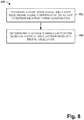
- the method 800 initiates at 802 with providing a start edge signal to a differential delay line to determine a fine tuning quantization or a fine time measurement.
- the fine tune measurement can be a bipolar measurement that results from a propagation of a start edge from a phase generator (e.g., phase generator 224) along delay chain elements (forming a positive chain) of the differential delay chain and a propagation of a stop edge along delay chain elements (a negative chain) in an opposite direction.
- the bipolar measurement can be generated in way that cancels any time delay or offset so that the delays chain elements are synchronized without mismatch.
- the start edge and the stop edge can be provided via the phase generator 224 of FIG. 2 without reliance on additional multiplexers being coupled to or in operation with the coarse time quantization measurements of the TDC.
- the coarse time quantization can be determined as a function of a modulated frequency signal from the low frequency portion of a modulator (e.g., a polar modulator) and the DCO periods of the digital oscillator.
- the method comprises determining a coarse tuning quantization or a coarse time measurement based on digital oscillation period(s) of a digital oscillator, which can be equidistant and also non-equidistant periods.
- the coarse quantization time can be generated to determine the start and stop final time measurement as a function of the DCO periods and a bipolar time measurement generated from a reference clock input and a divider input.
- a latching or a propagating of a start edge along the differential delay line can be controlled as a function of a start signal and a stop signal generated from a reference signal and a divider signal, wherein the divider signal is derived from a start and stop time measurement that is based on the propagation counts of the differential delay line as a function of the DCO periods of the DCO.
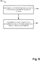
- the method 900 initiates at 902 with providing a differential delay line comprising a plurality of differential delay stages, which include a first delay element and a second delay element.
- DCO digitally controlled oscillator
- a phase generator provides a start edge to the plurality of differential delay stages of the differential delay line as a function of a DCO counter value generated by a DCO counter.
- a coarse time calculation component (e.g., 228) is configured to determine a coarse time measurement based on equidistant DCO periods of a DCO.
- the coarse time calculation component is configured to receive the DCO counter value from the DCO counter and generate a coarse quantization time of a DCO.
- the coarse time calculation component is configured to generate a final time measurement as a function of the coarse quantization time, a first binary conversion based on a first plurality of comparators of the differential delay line and a second binary conversion based on a second plurality of comparators of the differential delay line.
- the coarse time calculation component is further configured to recursively generate a DCO calculation based on the DCO counter value to facilitate a phase measurement, which can be represented along 360 degrees with a set of processing iterations.
- Examples can include subject matter such as a method, means for performing acts or blocks of the method, at least one machine-readable medium including instructions that, when performed by a machine cause the machine to perform acts of the method or of an apparatus or system for concurrent communication using multiple communication technologies according to embodiments and examples described herein.
- An example is a time to digital converter that comprises a delay line comprising a plurality of delay stages that include a first delay chain and a second delay chain to generate a fine time measurement of a digital oscillator of a phase locked loop.
- a coarse time calculation component is configured to generate a coarse time measurement based on equidistant periods and non-equidistant periods of the digital oscillator of the phase locked loop, wherein the fine time measurement and the coarse time measurement form a phase difference measurement of the phase locked loop that is communicated to the digital oscillator.
- An example further comprises an edge selector configured to enable a bipolar time measurement by generating a start edge, a stop edge and a sign value, wherein the start edge and the stop edge are generated based on a reference signal and a divider signal, and the sign value is generated based on a receiving order of receiving an edge of the reference signal and the divider signal, respectively.
- the coarse time calculation component is further configured to receive a digital oscillator counter value from a digital oscillator counter and generate the coarse time measurement of the digital oscillator based on the digital oscillator counter value and a modulated digital oscillator frequency from a frequency modulator.
- the coarse time calculation component is further configured to provide the coarse time measurement to a summing component to generate a final time measurement as the phase difference, wherein the final time measurement is derived from the coarse time measurement, a first binary conversion based on a first plurality of comparators of the delay line and a second binary conversion based on a second plurality of comparators of the delay line.
- the coarse time calculation component is further configured to recursively generate a digital oscillator calculation based on a digital oscillator counter value to generate a final time measurement as a phase measurement
- the delay line is configured to generate time measurements corresponding to different polarities for generation of a bipolar time measurement and cancel an offset resulting from at least one of a process, a temperature or a voltage dependency.
- the coarse time calculation component is further configured to generate the coarse time measurement based on a set of modulated frequency values from a polar modulator, a digital oscillator counter value and a sign value generated from an edge selector, wherein the coarse time calculation component utilizes the sign value to calculate a time of a non-constant digital oscillator period.
- An example which includes or omits optional elements of other examples , further comprising an edge selector configured to compare a reference signal of a reference clock and a divider signal of a divider clock and generate a start signal and a stop signal to a phase generator based thereon, and further configured to generate a sign value and provide the sign value to the coarse time calculation component, wherein the sign value is generated based on an order of a receiving edge of the reference signal and the divider signal, respectively.
- An example which includes or omits optional elements of other examples , further comprising a first set of comparators and a second set of comparators coupled to the plurality of delay stages configured to control different states of the plurality of delay stages based on a start edge and a stop edge that is provided by the phase generator.
- An example which includes or omits optional elements of other examples , further comprising a digital oscillator counter configured to count the periods of the digital oscillator and provide a count of the periods to the digital oscillator to determine the coarse time measurement.
- An example which includes or omits optional elements of other examples , further comprising a phase generator configured to control propagation and latching of delay line states of first delay elements and second delay elements of the plurality of delay stages based on a conversion of a received start signal and a received stop signal into a start edge and a stop edge that propagate along the plurality of delay stages, wherein the delay line is configured to generate a bipolar time measurement without an intrinsic offset.
- a phase generator configured to control propagation and latching of delay line states of first delay elements and second delay elements of the plurality of delay stages based on a conversion of a received start signal and a received stop signal into a start edge and a stop edge that propagate along the plurality of delay stages, wherein the delay line is configured to generate a bipolar time measurement without an intrinsic offset.
- phase generator and the delay line are further configured to cancel the intrinsic offset between processing a reference signal of a reference clock path and a divider signal of a divider clock path as a function of at least two DCO periods and the bipolar time measurement.
- phase generator is configured to inject the start edge to the plurality of delay stages of the delay line without utilizing a multiplexer for edge injection.
- phase generator is configured to control latching of delay line states of first delay elements and second delay elements of the plurality of delay stages as a function of a propagation mode and a latch mode and propagate the start edge and the stop edge in different directions with respect to one another along the delay line to generate the bipolar time measurement.
- An example which includes or omits optional elements of other examples , further comprising an edge selector component configured to generate a bipolar time measurement via the delay line based on a reference clock input of a reference clock path and a divider clock input of a divider clock path.
- An example is a mobile device comprising an antenna port, an RF-frontend, a digital baseband processor, and a digital phase locked loop in at least one of the RF-frontend and the digital baseband processor comprising a time to digital converter and a digital oscillator.
- the time to digital converter comprises a delay line comprising a plurality of delay stages that include a first delay element chain and a second delay element chain to generate a fine time measurement.
- a coarse time calculation component is configured to generate a coarse time quantization based on digital oscillator periods of the digital oscillator.
- the coarse time calculation component is further configured to generate the coarse time quantization based on the digital oscillator periods and a set of modulated frequency values of a frequency modulator.
- the coarse time calculation component is further configured to provide the coarse time quantization to an adder to generate a final time measurement with a first binary conversion of a first state of first delay elements of the delay line and a second binary conversion of a second state of second delay elements of the delay line.
- An example which includes or omits optional elements of other examples , further comprising a phase generator configured to provide a start edge and a stop edge to the plurality of delay stages of the delay line to generate the fine time quantization as a bipolar measurement via the delay line based on a received start signal and a received stop signal.
- An example which includes or omits optional elements of other examples , further comprising a phase generator configured to generate at least two timing measurements via the plurality of delay stages of the delay line based on a DCO rising edge or a DCO falling edge, and based on a start signal or a stop signal.
- phase generator generates the at least two timing measurements as bipolar measurements that propagate via the delay line in opposite directions to one another based on the start signal and the stop signal.
- An example which includes or omits optional elements of other examples , further comprising an edge selector configured to generate a start signal and a stop signal based on a reference signal and a divider signal, and a sign value based on an order of receiving the reference signal and the divider signal.
- the coarse time calculation component is configured to generate the coarse time quantization based on at least one of a set of frequency values of a frequency modulator, a digital oscillator counter value and a sign value, wherein the coarse time calculation component utilizes the sign value to calculate a time of a non-constant digital oscillator period.
- An example is a method comprising providing a start edge signal and a stop edge signal to a single delay line to determine a fine tuning quantization and determining a coarse tuning quantization based on digital oscillator periods of a digital oscillator of a phase locked loop.
- An example further comprises generating the coarse tuning quantization as a function of the digital oscillator periods, a set of modulated frequency values, a digital oscillator counter value and a sign value, wherein the sign value is determined based on a reception order of a divider signal and a reference signal at an edge selector.
- An example further comprises latching or propagating of a start edge along the single delay line as a function of a start signal and a stop signal generated at an edge selector from a reference signal and a divider signal.
- Apps can include routines, programs, components, data structures, etc., that perform particular tasks or implement particular abstract data types.
- operations disclosed can be practiced with other system configurations, including single-processor or multiprocessor systems, minicomputers, mainframe computers, as well as personal computers, hand-held computing devices, microprocessor-based or programmable consumer electronics, and the like, each of which can be operatively coupled to one or more associated mobile or personal computing devices.
- a computing device can typically include a variety of computer-readable media.
- Computer readable media can be any available media that can be accessed by the computer and includes both volatile and non-volatile media, removable and non-removable media.
- Computer-readable media can comprise computer storage media and communication media.
- Computer storage media includes both volatile and non-volatile, removable and non-removable media implemented in any method or technology for storage of information such as computer-readable instructions, data structures, program modules or other data.
- Computer storage media can include, but is not limited to, RAM, ROM, EEPROM, flash memory or other memory technology, CD ROM, digital versatile disk (DVD) or other optical disk storage, magnetic cassettes, magnetic tape, magnetic disk storage or other magnetic storage devices, or any other medium which can be used to store the desired information and which can be accessed by the computer.
- Communication media typically embodies computer-readable instructions, data structures, program modules or other data in a modulated data signal such as a carrier wave or other transport mechanism, and includes any information delivery media.
- modulated data signal means a signal that has one or more of its characteristics set or changed in such a manner as to encode information in the signal.
- communication media includes wired media such as a wired network or direct-wired connection, and wireless media such as acoustic, RF, infrared and other wireless media. Combinations of the any of the above should also be included within the scope of computer-readable media.
- Computer-readable media includes both computer storage media and communication media including any medium that facilitates transfer of a computer program from one place to another.
- a storage media may be any available media that can be accessed by a general purpose or special purpose computer.
- such computer-readable media can comprise RAM, ROM, EEPROM, CD-ROM or other optical disk storage, magnetic disk storage or other magnetic storage devices, or any other medium that can be used to carry or store desired program code means in the form of instructions or data structures and that can be accessed by a general-purpose or special-purpose computer, or a general-purpose or special-purpose processor. Also, any connection is properly termed a computer-readable medium.
- Disk and disc includes compact disc (CD), laser disc, optical disc, digital versatile disc (DVD), floppy disk and blu-ray disc where disks usually reproduce data magnetically, while discs reproduce data optically with lasers. Combinations of the above should also be included within the scope of computer-readable media.
- DSP digital signal processor
- ASIC application specific integrated circuit
- FPGA field programmable gate array
- a general-purpose processor may be a microprocessor, but, in the alternative, processor may be any conventional processor, controller, microcontroller, or state machine.
- a processor may also be implemented as a combination of computing devices, for example, a combination of a DSP and a microprocessor, a plurality of microprocessors, one or more microprocessors in conjunction with a DSP core, or any other such configuration. Additionally, at least one processor may comprise one or more modules operable to perform one or more of the acts and/or actions described herein.
- modules e.g., procedures, functions, and so on
- Software codes may be stored in memory units and executed by processors.
- Memory unit may be implemented within processor or external to processor, in which case memory unit can be communicatively coupled to processor through various means as is known in the art.
- at least one processor may include one or more modules operable to perform functions described herein.
- a CDMA system may implement a radio technology such as Universal Terrestrial Radio Access (UTRA), CDMA2000, etc.
- UTRA includes Wideband-CDMA (W-CDMA) and other variants of CDMA.
- W-CDMA Wideband-CDMA
- CDMA2000 covers IS-2000, IS-95 and IS-856 standards.
- a TDMA system may implement a radio technology such as Global System for Mobile Communications (GSM).
- GSM Global System for Mobile Communications
- An OFDMA system may implement a radio technology such as Evolved UTRA (E-UTRA), Ultra Mobile Broadband (UMB), IEEE 802.11 (Wi-Fi), IEEE 802.16 (WiMAX), IEEE 802.20, Flash-OFDM, etc.
- E-UTRA Evolved UTRA
- UMB Ultra Mobile Broadband
- IEEE 802.11 Wi-Fi
- WiMAX IEEE 802.16
- Flash-OFDM Flash-OFDM
- UTRA and E-UTRA are part of Universal Mobile Telecommunication System (UMTS).
- UMTS Universal Mobile Telecommunication System
- 3GPP Long Term Evolution (LTE) is a release of UMTS that uses E-UTRA, which employs OFDMA on downlink and SC-FDMA on uplink.
- UTRA, E-UTRA, UMTS, LTE and GSM are described in documents from an organization named " 3rd Generation Partnership Project" (3GPP ).
- CDMA2000 and UMB are described in documents from an organization named " 3rd Generation Partnership Project 2" (3GPP2 ).
- 3GPP2 3rd Generation Partnership Project 2
- wireless communication systems may additionally include peer-to-peer (e.g., mobile-to-mobile) ad hoc network systems often using unpaired unlicensed spectrums, 802.xx wireless LAN, BLUETOOTH and any other short- or long- range, wireless communication techniques.
- SC-FDMA Single carrier frequency division multiple access
- SC-FDMA Single carrier frequency division multiple access
- SC-FDMA has similar performance and essentially a similar overall complexity as those of OFDMA system.
- SC-FDMA signal has lower peak-to-average power ratio (PAPR) because of its inherent single carrier structure.
- PAPR peak-to-average power ratio
- SC-FDMA can be utilized in uplink communications where lower PAPR can benefit a mobile terminal in terms of transmit power efficiency.
- various aspects or features described herein may be implemented as a method, apparatus, or article of manufacture using standard programming and/or engineering techniques.
- article of manufacture as used herein is intended to encompass a computer program accessible from any computer-readable device, carrier, or media.
- computer-readable media can include but are not limited to magnetic storage devices (e.g., hard disk, floppy disk, magnetic strips, etc.), optical discs (e.g., compact disc (CD), digital versatile disc (DVD), etc.), smart cards, and flash memory devices (e.g., EPROM, card, stick, key drive, etc.).
- various storage media described herein can represent one or more devices and/or other machine-readable media for storing information.
- machine-readable medium can include, without being limited to, wireless channels and various other media capable of storing, containing, and/or carrying instruction(s) and/or data.
- a computer program product may include a computer readable medium having one or more instructions or codes operable to cause a computer to perform functions described herein.
- a software module may reside in RAM memory, flash memory, ROM memory, EPROM memory, EEPROM memory, registers, a hard disk, a removable disk, a CD-ROM, or any other form of storage medium known in the art.
- An exemplary storage medium may be coupled to processor, such that processor can read information from, and write information to, storage medium.
- storage medium may be integral to processor.
- processor and storage medium may reside in an ASIC.
- ASIC may reside in a user terminal.
- processor and storage medium may reside as discrete components in a user terminal.
- the acts and/or actions of a method or algorithm may reside as one or any combination or set of codes and/or instructions on a machine-readable medium and/or computer readable medium, which may be incorporated into a computer program product.
Description
- Phase-locked loops (PLLs) can provide precise generation and alignment of timing for a wide variety of applications. Digital phase-locked loops (DPLLs) are a viable alternative to traditional PLLs, in which a digital loop filter can be utilized to replace analog components. Further, time to digital converters (TDCs) can operate to digitally encode a phase error between reference and divider outputs. In ring oscillator based TDCs, power consumption and phase noise increase with measured time. The measure time of all digital phase locked loops (ADPLLs) is thus kept as small as possible to avoid power consumption and phase noise penalty. Because TDCs typically measure positive times, an additional TDC offset is normally introduced in front of a digital loop filter of the ADPLL, in which the TDC offset is chosen to give a margin for a multi-modulus divider (MMD) induced edge variation. A need exits therefore to overcome measure time induced power and phase noise penalty, while pursuing high resolution and high linearity in the TDC time-to-digital mapping characteristic with low power and low area in the implementation.
- Document
US 2009/0219073 A1 describes a high resolution time-to-digital converter. Further, documentUS2014/0091866 A1 describes a ring oscillator and documentWO 2007/093221 A1 describes a time-to-digital conversion with calibration pulse injection. DocumentUS 2014/055181 A1 describes a clock generating circuit includes: a counter that counts a number of pulses of an oscillation clock signal existed within one cycle of a reference clock signal; a first time-to-digital converter that generates a plurality of phases of first clock signals by delaying the oscillation clock signal; a second time-to-digital converter that generates a plurality of phases of second clock signals by delaying the oscillation clock signal by a short delay time; a third time-to-digital converter that generates a plurality of phases of third clock signals by delaying the delayed first clock signal; a delay control unit that outputs a delay control signal based on a difference between a cycle of the oscillation clock signal and a target cycle;; and an oscillator that generates, based on a cycle of the reference clock signal, the oscillation clock signal whose cycle is 1/m of the cycle of the reference clock signal. - The present invention, solving the issues of the prior art, is disclosed in
device claim 1 andmethod claim 12. Further embodiments are disclosed in the dependent claims. -
-
FIG. 1 illustrates an exemplary mobile communication device comprising at least an exemplary differential delay line; -
FIG. 2 illustrates an exemplary time to digital converter (TDC) in accordance with various aspects described; -
FIG. 3 illustrates timing operations of components of the TDC in accordance with various aspects described; -
FIG. 4 illustrates operations and binary conversions of components of the TDC in accordance with various aspects described; -
FIG. 5 illustrates timing operations of an edge selector component of the TDC in accordance with various aspects described; -
FIG. 6 illustrates timing operations of components of the TDC in accordance with various aspects described; -
FIG. 7 illustrates an example of the coarse time calculation component of the TDC in accordance with various aspects described; -
FIG. 8 illustrates an example method in accordance with various aspects described; and -
FIG. 9 illustrates a flow diagram of another exemplary method. - In consideration of the above described deficiencies and continued objectives, various aspects for TDCs are disclosed, which avoid having to digitally introduce a TDC offset in front of the PLL loop filter by facilitating bipolar time measurement techniques. This TDC offset normally operates to counteract the capability of TDCs to measure positive time differences only. However, the TDC offsets can be eliminated by systems and methods provided herein, which can be implemented in various components and systems, such as frequency modulated ADPLLs applicable in polar-modulators. In one embodiment, a digital oscillator (such as the oscillator of the DPLL employing the TDC) is utilized for determining a coarse time measurement/quantization that biases a phase locked loop before being locked in a frequency of operation (e.g., the reference frequency being synchronized to a feedback or divider frequency) by a fine tuning/timing measurement. A digital control oscillator calculation component is configured to calculate the coarse time measurement or a coarse tuning measurement from counted digital oscillator edges, even when the digital oscillator frequencies being received have been modulated (e.g., a polar frequency modulator or the like modulator). The low frequency part of a modulator (e.g., fractional sample rate converter of the modulator) can be used to calculate the coarse time measurements. An edge selector, a phase generator and a delay line can generate a bipolar time measurement (e.g., a sign value) for the fine tuning/timing measurement and generate a cancellation of an offset that depends on a process, a voltage or a temperature variance with respect to use, time or change of the system. Rather than having two or more linear TDCs for a positive measuring and a negative measuring of times and a fixed clock frequency, systems disclosed herein can operate as a bipolar time measuring single TDC with a single delay line that also facilitates a generation of bipolar time measurements, which indicate or represent different polarities based on a timing of a reception of a received reference signal edge or a received feedback/divider signal edge. In addition, the systems disclosed can determine the bipolar time measurement with modulated frequencies. Additional aspects and details of the disclosure are further described below with reference to the figures.
- Referring to
FIG. 1 , illustrated is an examplemobile communication device 100 that can operate in accordance with various aspects being disclosed. Themobile communication device 100, for example, comprises adigital baseband processor 102, anRF frontend 104 and anantenna port 108 for connecting to anantenna 106. Themobile communication device 100 can comprise an exemplary TDC 110 as part of thedigital baseband processor 102 or theRF frontend 104, which can also operate as a component within a DPLL for example. Nevertheless, it is also possible that each of thedigital baseband processor 102 and theRF frontend 104 comprises such a TDC 110 or even comprises more than one ofsuch TDC 110. TheRF frontend 104 is coupled to thedigital baseband processor 102 and theantenna port 108. - The TDC 110 can operate with a differential delay component that ensures there is no delay mismatch between a positive and negative input and output of the differential delay chain. In TDC topologies disclosed herein, the digital controlled oscillator (DCO) circulation counter can be used to determine a coarse time quantization or a coarse time measurement for coarse tuning without use of additional multiplexers for propagation or circulation counting. These advantages lead to a better phase noise performance, a symmetrical clock generation and a reduction in quantization noise. The quantization noise can be reduced when the
TDC 110 is used with a differential delay line of themobile communication device 100, which can operate to replace circulation or propagation counting by using the DCO for determining coarse time quantization. For example, the coarse quantization time can be calculated by the sum of the DCO periods of the DCO. - Further, the TDC 110 achieves a resolution enhancement, for example, when the TDC 110 is used for measuring time between certain events. Hence, the TDC 110 enables a more precise generation of clock signals in the
mobile communication device 100 and a more precise measuring of time differences (such as in a DPLL). The improved generation of clock signals and improved measuring of time differences enables a reduction of a noise floor in themobile communication device 100 and therefore improves or facilitates the overall performance of themobile communication device 100. - Referring now to
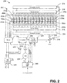
FIG. 2 , illustrated is an exemplary implementation of aTDC 200 as a fully differential multipath low-power bipolar delay line TDC in accordance with various aspects described. The TDC 200 comprises adifferential delay line 202 that operates to propagate a signal edge via differential delay stages 204a to 204n to facilitate measuring of times between at least two edges of the same or different signals. In one example, the time difference representing a phase error between a reference signal and a feedback signal in a DPLL is measured by theTDC 200. Although a differential delay line is contemplated, a single ended delay could also be embodied as the delay line. - In the configuration of the
delay line 202 of the present invention, the delay stages 204a to 204n each include afirst delay element 206a to 206n and asecond delay element 208a to 208n, which can represent one or more elements for each stage, such as for a differential chain ofdelay elements 206a to 206n or for 208a to 208n, for example. Thefirst delay elements 206a to 206n can be connected in series to form a first positive delay chain (e.g., a positive delay chain) of the differential delay line 202., while thesecond delay elements 208a to 208n can be connected in series to form a second negative delay chain (e.g., a negative delay chain) of thedifferential delay line 202. For example, the delay elements of thedifferential delay line 202 can comprise differential delay elements with a positive and a negative delay line or path that can be cross coupled at a positive input and a negative input of each delay element, in which the differential delay elements of the chains are free, independent of or without any mismatch. As such, each of the delays elements can be synchronized. - In another example configuration, the
differential delay line 202 can comprise a first plurality ofcomparators 210a to 210n, inputs of which are connected to the outputs of thefirst delay elements 206a to 206n. Thedifferential delay line 202 comprises a second plurality ofcomparators 212a to 212n and can be implemented to propagate signal edges without additional multiplexers. In detail, thedifferential delay line 202 comprises per delay stage an associatedcomparator 210a to 210n and 212a to 212n, a first input of which can be connected to an output of one of the delay elements of the associated delay stage 204a to 204n and a second input of which is connected to the other delay element of the associated delay stage 204a to 204n, as such each comparator can have a positive and negative input - Alternatively or additionally, in another example of the
differential delay line 202, inputs of every second comparator may be complementarily connected to the outputs of the associated delay stage with the inputs of the comparators associated to the preceding delay stage. As an example, a first input of a first comparator could be connected to the output of the first delay element of the first delay stage and a second input of the first comparator would be connected to the output of the second delay element of the first delay stage. According to the principle mentioned above, for a comparator being associated to a delay stage directly succeeding the first delay stage, the first input of this comparator could be connected to the output of the second delay element of the preceding delay stage and the second input of the comparator would be connected to the output of the first delay element of the preceding delay stage. - The
differential delay line 202 is configured to measure time differences such as a time between the insertion of the start edge and the occurrence of a stop signal, in which the insertion of the start and stop edges can be done directly into the line from aphase generator 224 without utilizing or independently of a multiplexer between the phase generator and thedifferential delay line 202. A complementary circuiting of the inputs of the comparators or the outputs of the comparators being associated to directly succeeding delay stages, as discussed in the above example configurations, can facilitate a hot onedecoder differential delay line 202. The TDC 200 comprises a top hot onedecoder 214 and a bottom hot onedecoder 216, a top thermo tobinary decoder 218 and a bottom thermo tobinary decoder 220. Rather than thedifferential delay line 202 comprising additional multiplexers to count propagations or oscillations of a signal edge, theTDC 200 utilizes a DCO circulation counting for coarse time quantization and initiating the start and stop edges to the delay line via thephase generator 224. TheTDC 200 thus avoids power hungry and phase noise degrading ring oscillator circulations for coarse time quantization and avoids circulation determinations from a top and bottom counter. - In one embodiment, the coarse quantization time tm_dco can be determined as a function of the DCO periods of a
DCO 230 coupled to thedelay line 202 as in the following equation:
DCO 230 and i is the DCO counter value of aDCO counter 226, which can also be represented as (n) herein, as illustrated inFIG. 2 . - The differential implementation of the
TDC 200 can be used, for example, for an all-digital wireless PLL (ADPLL). The time todigital converter 200 can operate to measure the time between the rising edge of the 26 MHz reference clock and the rising edge of a divider edge such as a multi modulus divider (MMD) edge. - An
edge selector 222 provides a start signal and a stop signal to thephase generator 224, which, in turn, generates a start edge and a stop edge into thedifferential delay line 202 in response to receiving the start signal and the stop signal. Theedge selector 222 is therefore configured to compare a reference signal of a reference clock (Ref clk) and a divider signal of a divider clock (Div_clk) and generate the start signal and the stop signal to aphase generator 224. Furthermore, theedge selector 222 generates a sign value (sign) to a coarse time calculation component (labelled Tm_DCO calculation) 228, in which the sign value is based on an order of receiving the reference signal and the divider signal as a bipolar time measurement, as further detailed below. - In the example shown in
FIG. 2 , thedifferential delay line 202 can comprise multiple different delay stages 204a to 204n with a unit delay, for example, of about 8 picoseconds or other delay. Thedifferential delay line 202 comprises, for example, a sufficient number of delay elements to accommodate or handle a maximal DCO period divided by 2 or 4, for example, as represented by thedivision component 232. After starting thedifferential delay line 202, the start edge propagates at least partially through the differential delay stages 204a to 204n to an extent according to DCO edges of theDCO 230, such as a DCO rising edge or a DCO falling edge of theDCO 230. The polarity of the edge can change or reverse after each circulation or propagation through thedifferential delay line 202, which is also based on a rising or a falling DCO edge. In this manner, positive and negative determinations can come from a reuse of the same delay line that facilitates the offset cancelation. In addition, a bipolar measurement is generated from theedge selector block 222, which is discussed further below, for further determining a coarse time quantization. - In the example of measuring the time between the rising edge a reference clock (e.g., 26 MHz) and the rising edge of a divider edge, the stop edge or stop signal is derived from a next rising DCO edge. The stop signal denoted as
Stop_Ticks 1 andStop_Ticks 2 from thephase generator 224 results from theedge selector 222 and is a function of a next rising edge of theDCO 230. The Stop Ticks 1 and StopTicks 2 signals trigger thecomparators 210a to 210n and 212a to 212n to latch current states of the delay stages, for example. The hot onedecoder binary decoders decoder - The
phase generator 224 of theTDC 200 controls the propagating and latching of the delay stages 204a to 204n via a propagation mode and a latching mode as a function of a start and stop signal provided by theedge selector 222 and a DCO edge of theDCO 230. For example, as illustrated inFIG. 3 , astart signal 302 is initiated by theedge selector 222 to thephase generator 224. As a result, thephase generator 224 converts thestart signal 302 into astart_p signal 306 and astart_n signal 308 as a positive start_p edge and a negative start_n edge, for example. The positive differential edge propagates (Ticks 1 316) along thedifferential delay line 202 at the conversion of thestart signal 302 to a start delay line plus (start DL +) until the first subsequent rising DCO edge latches the Delay Line states with thecomparators 210a to 210n (Tick1 comparators). The latching in a latch mode of thedelay line 202 is initiated by first subsequent DCO edge after thepositive start signal 306 initiates propagating, for example. - A
conversion result 402 of the comparator latching is denoted asComp_tick1 402, as illustrated inFIG. 4 . TheHot One Decoder 214 converts the first Comp_tick1 402 (1 / 0) transition into a hot onecode 404. The hot onecode 404 is converted by the thermo tobin decoder 218 in a binary Ticks1 value of theTicks 1propagation 316, as illustrated inFIG. 3 . - Further, a rising
stop edge 304 is received by thephase generator 224 from theedge selector 222. Thephase generator 224 converts thestop signal 304 into a falling edge at the start signal 306 start_p and a rising edge at thestart signal 308 start n. This second differential edge (conversion of stop signal 304) has an opposite direction in comparison to the first differential edge (conversion of start signal 302) and propagates along thedifferential delay line 202 as shown atTicks2 318 until the next risingDCO edge 310 initiates subsequent to thestop signal 304 facilitates astop_Ticks2 signal 314, which causes a latching mode of thedelay line 202 that operates to latch thedelay line 202 state with thecomparators 212a to 212n respectively (denoted also as correspondingTicks2 comparators). The latch result, or the latched/locked state, is denoted as abinary signal 406 inFIG. 4 or as Comp_ticks2. As theTick2 comparators 212a to 212n are in opposite direction in connection to thedelay line 202, they are affected by the negative differential edge flipped delay-elements 208a to 208n, which appear positive in theComp_Tick2 conversion result 406. Subsequent to the latching ofTicks2 318 by theDCO edge 310, the hot onedecoder 216 converts the first Comp_tick2 (1 / 0) transition into thebinary code 406, a Hot onecode 1. The hot onecode 406 is then converted by the thermo tobin decoder 220 into a binary Ticks2 value of the opposingTicks 2propagation 318. - The final time measurement (i.e., Result) can be represented as the final start/stop time tstart stop, which is calculated as a function of ttm_DCO, tticks1, tticks2 and Δt, wherein Δt is the delay of one unity delay element 204a of delay elements 204a to 204n, or 208a to 208n. The unity delay time Δt can be used to calculate tticks1 = ticks1 ∗ Δt, and tticks2=ticks2∗ Δt, while ticks1 (Ticks1) and ticks2 (Ticks2) are the binary values from conversion. In one example, the tstart stop is determined according to following:

- In one aspect, the
TDC 200 operates to determine the coarse quantization time of the delay line as a function of the digital controlledoscillator 230, which is represented by Eqn. 1 above. The counting of propagations of thedelay line 202 is replaced by theDCO 230, theDCO counter 226 and a coarsetime calculation component 228 for determining ttm_DCO. The advantage of such an architecture is that the circulation counting or propagation counting is performed without multiplexers being assigned to such functions. The propagation counting is determined independent of multiplexers. The final time measure or start and stop time tstart stop of the delay line for latching and propagation modes and phase measurement is performed by the same delay line via measurements of Ticks1 and Ticks2, which is further a function of thesame phase generator 224. - The below Eqn. 3 illustrates offset cancellation of the Result or final start stop time measurement as a result of the advantages of having the
same delay line 202 for providing a binary conversion from the thermo tobin decoders single phase generator 224 as a function of theDCO 230 andDCO counter 224. This offset cancellation via thedelay line 202 enables a linear offset free TDC, which can operate to measure positive times.
- The
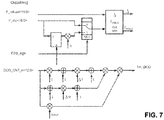
edge selector 222 is configured to compare a reference clock and a divider clock. In response to the comparison, theedge selector 222 generates a start signal or a stop signal to thephase generator 224 and to alogic gate 233 to enable theDCO counter 226, as well as a bipolar time measurement as a sign value (sign) to the coarsetime calculation component 228. - For example,
FIG. 5 illustrates timing diagrams 500 of theedge selector 222 ofFIG. 2 for generating a sign value for the determination of the coarse time measurement via the coarsetime calculation component 228. Theedge selector 222 receives thereference clock input divider clock input Case 1, the first rising edge on thereference clock 502 triggers thestart signal 506, while inCase 2, the first rising edge being thedivider clock 514 triggers thestart signal 516. If the divider clock edge is earlier than the reference clock edge, as inCase 2 ofdivider clock edge 514 andreference clock edge 512, then the sign signal or sign value is one (e.g., sign signal 520). Thesign signal 520 indicates that there is a negative time differential tm between thereference edge 512 and the divider edge 514 (i.e., the reference clock edge or ref clk edge trails the divider clock edge or div clk edge).Case 1 is a positive case, in which thereference clock edge 502 is earlier than the divider clock edge 504 (i.e., the ref clk edge leads the div clk edge), and thus a positive time differential tm and thesign signal 510 is generated as a negative output sign. Thesignals time calculation component 228 for generating the coarse time measurement based on the sign value or sign signal Theedge selector 222 further operates to convert thereference clock inputs divider clock inputs signals - In one aspect, the
TDC 200 can generate time measurements of different polarity for a bipolar time measurement and further cancel an offset that results from at least one of a process, a temperature and/or a voltage dependency. For example, a digital TDC gain calibration can be used (e.g., coarse time calculation component), to overcome the unity delay Δt process temperature voltage (PVT) dependency. Without compensating for the unity delay Δt PVT dependency, the gain of the TDC would vary and the TDC would be unable to match the DCO coarse time tm_dco with the time measurements or bipolar measurement (e.g., Ticks 1 and Ticks 2) of the TDC, resulting in a mismatch therebetween. However, the delay line can be configured to cancel any intrinsic offset due to PVT variations with the unit delay time. In the digital gain calibration, the unity delay Δt can be determined by measuring two different DCO periods t1 and t2, withticks 1 and ticks2 according to equation (4) as follows:
- The time Δt is used to calculated tstart_stop, such as via the coarse
time calculation component 228, which is afterwards normalized with Δtnorm = 2ps to tnorm according to equation (5) as follows:
FIG. 6 illustrates various aspects of theDCO counter 226 ofFIG. 2 . As can be seen, when astart edge 302 is initiated by theedge selector 222, the edge is propagated through thedelay line 202 until the first rising DCO edge of theDCO 230 latches thecomparators 210a to 210n, aTicks 1value 316 is determined and the DCO counter 226 counts the DCO periods according to the DCO edges. In response to a stop signal being initiated and thecomparators 212a to 212n (depending on the period length) being latched concurrent to the propagation (e.g., a negative propagation or reverse propagation), theDCO counter 226 halts counting 602 and Ticks2 is determined. A delay line length can be determined by the DCO clock divided by 2 or 4 depending on the selected band, which lead to frequency range of 700 MHz up to 1500 MHz. As such, thedelay line 202 handles up to 1.5ns measure time. - Referring back to
FIG. 2 , the modulator (e.g., a polar modulator) or the FMOD/FSRC component 240 as a low frequency component of a modulator can operate to receive amplitude and frequency modulation data (AM-Data) and (FMOD-Data) as calculated by a coordinate rotation digital computer component (CORDIC) (not shown) on a 104 MHz clock rate. The data can be interpolated on a modulated DCO clock rate divided by 4, denoted as fDCO/4, with a linear fractional samplerate converter FSRC 240 in an FM Path and a quadratic FSRC in an AM-Path, for example. The linear FSRC high-frequency part can be reloaded with the initial frequency value (reload) freload, increment value (inc) fine and reload cycles from an oscillator. The high-frequency FSRC can be clocked with fDCO/4, in which for each rising edge a new frequency word is calculated according to equation (6).
- A reload cycle counter of the FMOD/FSRC component or
modulator 240 can be initialized at a reload event with a reload cycle value from an oscillator (e.g., an NCO) and can be decreased with each rising edge of fDCO/4. A reload event can be created to generate the set of reload values (reload cycle values, freload and fine) when a counter to the NCO is initialized, for example. - The coarse
time calculation component 228 ofFIG. 2 is configured to receive thesign signal FIG. 5 and compute the DCO calculation Tm_dco as a function of the sign signal being 510 or 520, a DCO counter value (e.g., n) from theDCO counter 226, and a set of reload values (freload, finc) or modulated frequency values from the FMOD/FSRC component 240. The coarsetime calculation component 228 utilizes the sign value to calculate a time of a non-constant/non-equidistant periods of the digital oscillator periods. The DCP periods of the DCO can be equidistant and non-equidistant. The DCO periods, for example, can be non-equidistant from one another when the PLL is used in a polar modulator with a modulation of amplitude and phase. In applying the phase shift in modulation, different frequency words are applied to the DCO by which to change the period. When the periods are changing, such as inFIG. 6 with different periods or non-equidistant periods t1, t2, and t3, for example, each of these are not equivalent, so information related to the length of each is obtained for calculating the Tm DCO. For example, Eqn. 7 below provides a sum of all the periods, in which 1/f is in the digital domain and thus the additional equations are performed with a Taylor series. - In describing the coarse
time calculation component 228, various assumptions can be ascribed for the calculation of Tm_DCO. In one embodiment, the reference clock input to theedge selector 222 can be about 26 MHz with negligible or without any offset to theDCO 230 comprising about a 104 MHz digital clock. Therefore, at every 26 MHz rising edge reload values freload and fine can be available. Additionally, all digital processing delay offset can be compensated for. The Tm_DCO calculation can thus be done on 26MHz rising reference clock edge. The coarsetime calculation component 228 can therefore generate an output as a propagation count of the differential delay line as a function of a DCO periods of theDCO 230. The coarsetime calculation component 228 generates the coarse quantization time of the DCO as a propagation counter of the differential delay line based on the reload values freload and finc from low-frequency FSRC side of a frequency modulation and fractional sample rate converter (FMOD/FSRC)component 240, the sign value ofedge selector component 222, and the DCO Counter value n. The time Tm_DCO is furthermore a function of a sum of ti the DCO periods divided by the by fourdivisor 232, which can be represented as 1/fi. The FSRC component calculates the DCO frequencies fi with 1GHz clock rate, while calculating the inversion of fi leads to a huge current consumption in digital part. Therefore a tertiary or third ordered Taylor series approximation can be used to implement the inversion, as in the equation (10) below, in which the following summations:


- Referring now to
FIG. 7 , illustrated is an example of a coarsetime calculation component 228 comprising a mux, multipliers and adders running at a 26 MHz reference clock. In one aspect, a Horner schema enables a digital implementation of Tm_DCO calculation component 228 with only 6 multipliers and 5 adders running at the 26 MHz reference clock. A sign bit equal to one indicates that a divider edge such as a Multi Modulus Divider edge appears before reference clock edge; therefore finc from a previous reload is used and multiplied by -1. The DCO_CNT corresponds to the counter value, ESB sign corresponds to the sign value from theedge selector 222, while F reload and F_inc designate frequency signal values from a low frequency part of a frequency modulator (e.g., Fractional Sample Rate Converter), which are modulated and used to determine the coarse time measurement (Tm DCO).


- In another aspect, the coarse
time calculation component 228 of theTDC 200 is configured to compute up to 90 degrees of 360 degrees because in one 26 MHz period the FSRC is able to be reloaded (e.g., reload values) four times as the FMOD/FSRC component 240 receives data from a CORDIC on a 104 MHz clock rate. Other implementations can also be envisioned according to different clock rates, for example.
The coarsetime calculation component 228, for example, compares the DCO counter value (n, or DCO_CNT_n) from theDCO counter 226 with a first set of reload cycle values (e.g., freload, finc). If the DCO counter value (n) is larger than the first reload cycle value (e.g., freload), then the first reload cycle value is used to factor T m_DCO1 . For example, the reload cycle value can be subtracted from the DCO counter value. If the DCO-counter value is larger than a second reload cycle value, then T m_DCO2 can be factored with the second set of reload cycles and the DCO counter, in which the DCO counter value can be reduced by the second reload cycle value, for example. If the DCO counter value is larger than a third reload cycle value, then the third recycle value can be utilized and the DCO counter value reduced or factored by the third reload value for determining T m_DCO3 for example. The procedure is then iteratively repeated again. The propagation counter count or a coarse quantization time total Tm_DCOTOTAL can be recursively calculated by the coarse time calculation component, which enables a 360° phase measurement. A delay line length can also be determined by the DCO clock divided by 2/4 depending on the selected band, which leads to frequency range of 700 MHz up to 1500 MHz. Therefore the delay line operates to handle up to about 1 to 5ns, such as 1.5ns measure time. - While the methods described within this disclosure are illustrated in and described herein as a series of acts or events, it will be appreciated that the illustrated ordering of such acts or events are not to be interpreted in a limiting sense. For example, some acts may occur in different orders and/or concurrently with other acts or events apart from those illustrated and/or described herein. In addition, not all illustrated acts may be required to implement one or more aspects or embodiments of the description herein. Further, one or more of the acts depicted herein may be carried out in one or more separate acts and/or phases.
- Referring to
FIG. 8 , illustrated is an example method for utilizing a DCO for a coarse time measurement in a TDC in accordance with various aspects described. Themethod 800 initiates at 802 with providing a start edge signal to a differential delay line to determine a fine tuning quantization or a fine time measurement. The fine tune measurement can be a bipolar measurement that results from a propagation of a start edge from a phase generator (e.g., phase generator 224) along delay chain elements (forming a positive chain) of the differential delay chain and a propagation of a stop edge along delay chain elements (a negative chain) in an opposite direction. The bipolar measurement can be generated in way that cancels any time delay or offset so that the delays chain elements are synchronized without mismatch. - In one embodiment, the start edge and the stop edge can be provided via the
phase generator 224 ofFIG. 2 without reliance on additional multiplexers being coupled to or in operation with the coarse time quantization measurements of the TDC. For example, the coarse time quantization can be determined as a function of a modulated frequency signal from the low frequency portion of a modulator (e.g., a polar modulator) and the DCO periods of the digital oscillator. - At 804, the method comprises determining a coarse tuning quantization or a coarse time measurement based on digital oscillation period(s) of a digital oscillator, which can be equidistant and also non-equidistant periods. The coarse quantization time can be generated to determine the start and stop final time measurement as a function of the DCO periods and a bipolar time measurement generated from a reference clock input and a divider input.
- A latching or a propagating of a start edge along the differential delay line can be controlled as a function of a start signal and a stop signal generated from a reference signal and a divider signal, wherein the divider signal is derived from a start and stop time measurement that is based on the propagation counts of the differential delay line as a function of the DCO periods of the DCO.
- Referring to
FIG. 9 , illustrated is another example method for utilizing a digitally controlled oscillator (DCO) for a coarse time measurement in a TDC in accordance with various aspects described. Themethod 900 initiates at 902 with providing a differential delay line comprising a plurality of differential delay stages, which include a first delay element and a second delay element. - At 904, a phase generator provides a start edge to the plurality of differential delay stages of the differential delay line as a function of a DCO counter value generated by a DCO counter.
- A coarse time calculation component (e.g., 228) is configured to determine a coarse time measurement based on equidistant DCO periods of a DCO. The coarse time calculation component is configured to receive the DCO counter value from the DCO counter and generate a coarse quantization time of a DCO. The coarse time calculation component is configured to generate a final time measurement as a function of the coarse quantization time, a first binary conversion based on a first plurality of comparators of the differential delay line and a second binary conversion based on a second plurality of comparators of the differential delay line. The coarse time calculation component is further configured to recursively generate a DCO calculation based on the DCO counter value to facilitate a phase measurement, which can be represented along 360 degrees with a set of processing iterations.
- Examples can include subject matter such as a method, means for performing acts or blocks of the method, at least one machine-readable medium including instructions that, when performed by a machine cause the machine to perform acts of the method or of an apparatus or system for concurrent communication using multiple communication technologies according to embodiments and examples described herein.
- An example is a time to digital converter that comprises a delay line comprising a plurality of delay stages that include a first delay chain and a second delay chain to generate a fine time measurement of a digital oscillator of a phase locked loop. A coarse time calculation component is configured to generate a coarse time measurement based on equidistant periods and non-equidistant periods of the digital oscillator of the phase locked loop, wherein the fine time measurement and the coarse time measurement form a phase difference measurement of the phase locked loop that is communicated to the digital oscillator.
- An example further comprises an edge selector configured to enable a bipolar time measurement by generating a start edge, a stop edge and a sign value, wherein the start edge and the stop edge are generated based on a reference signal and a divider signal, and the sign value is generated based on a receiving order of receiving an edge of the reference signal and the divider signal, respectively.
- An example, which includes or omits optional elements of other examples, wherein the coarse time calculation component is further configured to receive a digital oscillator counter value from a digital oscillator counter and generate the coarse time measurement of the digital oscillator based on the digital oscillator counter value and a modulated digital oscillator frequency from a frequency modulator.
- An example, which includes or omits optional elements of other examples , wherein the coarse time calculation component is further configured to provide the coarse time measurement to a summing component to generate a final time measurement as the phase difference, wherein the final time measurement is derived from the coarse time measurement, a first binary conversion based on a first plurality of comparators of the delay line and a second binary conversion based on a second plurality of comparators of the delay line.
- An example, which includes or omits optional elements of other examples , wherein the coarse time calculation component is further configured to recursively generate a digital oscillator calculation based on a digital oscillator counter value to generate a final time measurement as a phase measurement, wherein the delay line is configured to generate time measurements corresponding to different polarities for generation of a bipolar time measurement and cancel an offset resulting from at least one of a process, a temperature or a voltage dependency.
- An example, which includes or omits optional elements of other examples , wherein the coarse time calculation component is further configured to generate the coarse time measurement based on a set of modulated frequency values from a polar modulator, a digital oscillator counter value and a sign value generated from an edge selector, wherein the coarse time calculation component utilizes the sign value to calculate a time of a non-constant digital oscillator period.
- An example, which includes or omits optional elements of other examples , further comprising an edge selector configured to compare a reference signal of a reference clock and a divider signal of a divider clock and generate a start signal and a stop signal to a phase generator based thereon, and further configured to generate a sign value and provide the sign value to the coarse time calculation component, wherein the sign value is generated based on an order of a receiving edge of the reference signal and the divider signal, respectively.
- An example, which includes or omits optional elements of other examples , further comprising a first set of comparators and a second set of comparators coupled to the plurality of delay stages configured to control different states of the plurality of delay stages based on a start edge and a stop edge that is provided by the phase generator.
- An example, which includes or omits optional elements of other examples , further comprising a digital oscillator counter configured to count the periods of the digital oscillator and provide a count of the periods to the digital oscillator to determine the coarse time measurement.
- An example, which includes or omits optional elements of other examples , further comprising a phase generator configured to control propagation and latching of delay line states of first delay elements and second delay elements of the plurality of delay stages based on a conversion of a received start signal and a received stop signal into a start edge and a stop edge that propagate along the plurality of delay stages, wherein the delay line is configured to generate a bipolar time measurement without an intrinsic offset.
- An example, which includes or omits optional elements of other examples , wherein the phase generator and the delay line are further configured to cancel the intrinsic offset between processing a reference signal of a reference clock path and a divider signal of a divider clock path as a function of at least two DCO periods and the bipolar time measurement.
- An example, which includes or omits optional elements of other examples , wherein the phase generator is configured to inject the start edge to the plurality of delay stages of the delay line without utilizing a multiplexer for edge injection.
- An example, which includes or omits optional elements of other examples , wherein the phase generator is configured to control latching of delay line states of first delay elements and second delay elements of the plurality of delay stages as a function of a propagation mode and a latch mode and propagate the start edge and the stop edge in different directions with respect to one another along the delay line to generate the bipolar time measurement.
- An example, which includes or omits optional elements of other examples , further comprising an edge selector component configured to generate a bipolar time measurement via the delay line based on a reference clock input of a reference clock path and a divider clock input of a divider clock path.
- An example is a mobile device comprising an antenna port, an RF-frontend, a digital baseband processor, and a digital phase locked loop in at least one of the RF-frontend and the digital baseband processor comprising a time to digital converter and a digital oscillator. The time to digital converter comprises a delay line comprising a plurality of delay stages that include a first delay element chain and a second delay element chain to generate a fine time measurement. A coarse time calculation component is configured to generate a coarse time quantization based on digital oscillator periods of the digital oscillator.
- An example, wherein the coarse time calculation component is further configured to generate the coarse time quantization based on the digital oscillator periods and a set of modulated frequency values of a frequency modulator.
- An example, which includes or omits optional elements of other examples , wherein the coarse time calculation component is further configured to provide the coarse time quantization to an adder to generate a final time measurement with a first binary conversion of a first state of first delay elements of the delay line and a second binary conversion of a second state of second delay elements of the delay line.
- An example, which includes or omits optional elements of other examples , further comprising a phase generator configured to provide a start edge and a stop edge to the plurality of delay stages of the delay line to generate the fine time quantization as a bipolar measurement via the delay line based on a received start signal and a received stop signal.
- An example, which includes or omits optional elements of other examples , further comprising a phase generator configured to generate at least two timing measurements via the plurality of delay stages of the delay line based on a DCO rising edge or a DCO falling edge, and based on a start signal or a stop signal.
- An example, which includes or omits optional elements of other examples , wherein the phase generator generates the at least two timing measurements as bipolar measurements that propagate via the delay line in opposite directions to one another based on the start signal and the stop signal.
- An example, which includes or omits optional elements of other examples , further comprising an edge selector configured to generate a start signal and a stop signal based on a reference signal and a divider signal, and a sign value based on an order of receiving the reference signal and the divider signal.
- An example, which includes or omits optional elements of other examples , wherein the coarse time calculation component is configured to generate the coarse time quantization based on at least one of a set of frequency values of a frequency modulator, a digital oscillator counter value and a sign value, wherein the coarse time calculation component utilizes the sign value to calculate a time of a non-constant digital oscillator period.
- An example is a method comprising providing a start edge signal and a stop edge signal to a single delay line to determine a fine tuning quantization and determining a coarse tuning quantization based on digital oscillator periods of a digital oscillator of a phase locked loop.
- An example further comprises generating the coarse tuning quantization as a function of the digital oscillator periods, a set of modulated frequency values, a digital oscillator counter value and a sign value, wherein the sign value is determined based on a reception order of a divider signal and a reference signal at an edge selector.
- An example further comprises latching or propagating of a start edge along the single delay line as a function of a start signal and a stop signal generated at an edge selector from a reference signal and a divider signal.
- Applications (e.g., program modules) can include routines, programs, components, data structures, etc., that perform particular tasks or implement particular abstract data types. Moreover, those skilled in the art will appreciate that the operations disclosed can be practiced with other system configurations, including single-processor or multiprocessor systems, minicomputers, mainframe computers, as well as personal computers, hand-held computing devices, microprocessor-based or programmable consumer electronics, and the like, each of which can be operatively coupled to one or more associated mobile or personal computing devices.
- A computing device can typically include a variety of computer-readable media. Computer readable media can be any available media that can be accessed by the computer and includes both volatile and non-volatile media, removable and non-removable media. By way of example and not limitation, computer-readable media can comprise computer storage media and communication media. Computer storage media includes both volatile and non-volatile, removable and non-removable media implemented in any method or technology for storage of information such as computer-readable instructions, data structures, program modules or other data. Computer storage media (e.g., one or more data stores) can include, but is not limited to, RAM, ROM, EEPROM, flash memory or other memory technology, CD ROM, digital versatile disk (DVD) or other optical disk storage, magnetic cassettes, magnetic tape, magnetic disk storage or other magnetic storage devices, or any other medium which can be used to store the desired information and which can be accessed by the computer.
- Communication media typically embodies computer-readable instructions, data structures, program modules or other data in a modulated data signal such as a carrier wave or other transport mechanism, and includes any information delivery media. The term "modulated data signal" means a signal that has one or more of its characteristics set or changed in such a manner as to encode information in the signal. By way of example, and not limitation, communication media includes wired media such as a wired network or direct-wired connection, and wireless media such as acoustic, RF, infrared and other wireless media. Combinations of the any of the above should also be included within the scope of computer-readable media.
- It is to be understood that aspects described herein may be implemented by hardware and optionally software and/or firmware. When implemented in software, functions may be stored on or transmitted over as one or more instructions or code on a computer-readable medium. Computer-readable media includes both computer storage media and communication media including any medium that facilitates transfer of a computer program from one place to another. A storage media may be any available media that can be accessed by a general purpose or special purpose computer. By way of example, and not limitation, such computer-readable media can comprise RAM, ROM, EEPROM, CD-ROM or other optical disk storage, magnetic disk storage or other magnetic storage devices, or any other medium that can be used to carry or store desired program code means in the form of instructions or data structures and that can be accessed by a general-purpose or special-purpose computer, or a general-purpose or special-purpose processor. Also, any connection is properly termed a computer-readable medium. For example, if software is transmitted from a website, server, or other remote source using a coaxial cable, fiber optic cable, twisted pair, digital subscriber line (DSL), or wireless technologies such as infrared, radio, and microwave, then coaxial cable, fiber optic cable, twisted pair, DSL, or wireless technologies such as infrared, radio, and microwave are included in the definition of medium. Disk and disc, as used herein, includes compact disc (CD), laser disc, optical disc, digital versatile disc (DVD), floppy disk and blu-ray disc where disks usually reproduce data magnetically, while discs reproduce data optically with lasers. Combinations of the above should also be included within the scope of computer-readable media.
- Various illustrative logics, logical blocks, modules, and circuits described in connection with aspects disclosed herein may be implemented or performed with a general purpose processor, a digital signal processor (DSP), an application specific integrated circuit (ASIC), a field programmable gate array (FPGA) or other programmable logic device, discrete gate or transistor logic, discrete hardware components, or any combination thereof designed to perform functions described herein. A general-purpose processor may be a microprocessor, but, in the alternative, processor may be any conventional processor, controller, microcontroller, or state machine. A processor may also be implemented as a combination of computing devices, for example, a combination of a DSP and a microprocessor, a plurality of microprocessors, one or more microprocessors in conjunction with a DSP core, or any other such configuration. Additionally, at least one processor may comprise one or more modules operable to perform one or more of the acts and/or actions described herein.
- For a software implementation, techniques described herein may be implemented with modules (e.g., procedures, functions, and so on) that perform functions described herein. Software codes may be stored in memory units and executed by processors. Memory unit may be implemented within processor or external to processor, in which case memory unit can be communicatively coupled to processor through various means as is known in the art. Further, at least one processor may include one or more modules operable to perform functions described herein.
- Techniques described herein may be used for various wireless communication systems such as CDMA, TDMA, FDMA, OFDMA, SC-FDMA and other systems. The terms "system" and "network" are often used interchangeably. A CDMA system may implement a radio technology such as Universal Terrestrial Radio Access (UTRA), CDMA2000, etc. UTRA includes Wideband-CDMA (W-CDMA) and other variants of CDMA. Further, CDMA2000 covers IS-2000, IS-95 and IS-856 standards. A TDMA system may implement a radio technology such as Global System for Mobile Communications (GSM). An OFDMA system may implement a radio technology such as Evolved UTRA (E-UTRA), Ultra Mobile Broadband (UMB), IEEE 802.11 (Wi-Fi), IEEE 802.16 (WiMAX), IEEE 802.20, Flash-OFDM, etc. UTRA and E-UTRA are part of Universal Mobile Telecommunication System (UMTS). 3GPP Long Term Evolution (LTE) is a release of UMTS that uses E-UTRA, which employs OFDMA on downlink and SC-FDMA on uplink. UTRA, E-UTRA, UMTS, LTE and GSM are described in documents from an organization named "3rd Generation Partnership Project" (3GPP). Additionally, CDMA2000 and UMB are described in documents from an organization named "3rd ). Further, such wireless communication systems may additionally include peer-to-peer (e.g., mobile-to-mobile) ad hoc network systems often using unpaired unlicensed spectrums, 802.xx wireless LAN, BLUETOOTH and any other short- or long- range, wireless communication techniques.
- Single carrier frequency division multiple access (SC-FDMA), which utilizes single carrier modulation and frequency domain equalization is a technique that can be utilized with the disclosed aspects. SC-FDMA has similar performance and essentially a similar overall complexity as those of OFDMA system. SC-FDMA signal has lower peak-to-average power ratio (PAPR) because of its inherent single carrier structure. SC-FDMA can be utilized in uplink communications where lower PAPR can benefit a mobile terminal in terms of transmit power efficiency.
- Moreover, various aspects or features described herein may be implemented as a method, apparatus, or article of manufacture using standard programming and/or engineering techniques. The term "article of manufacture" as used herein is intended to encompass a computer program accessible from any computer-readable device, carrier, or media. For example, computer-readable media can include but are not limited to magnetic storage devices (e.g., hard disk, floppy disk, magnetic strips, etc.), optical discs (e.g., compact disc (CD), digital versatile disc (DVD), etc.), smart cards, and flash memory devices (e.g., EPROM, card, stick, key drive, etc.). Additionally, various storage media described herein can represent one or more devices and/or other machine-readable media for storing information. The term "machine-readable medium" can include, without being limited to, wireless channels and various other media capable of storing, containing, and/or carrying instruction(s) and/or data. Additionally, a computer program product may include a computer readable medium having one or more instructions or codes operable to cause a computer to perform functions described herein.
- Further, the acts and/or actions of a method or algorithm described in connection with aspects disclosed herein are embodied directly in hardware, and optionally in a software module executed by a processor. A software module may reside in RAM memory, flash memory, ROM memory, EPROM memory, EEPROM memory, registers, a hard disk, a removable disk, a CD-ROM, or any other form of storage medium known in the art. An exemplary storage medium may be coupled to processor, such that processor can read information from, and write information to, storage medium. In the alternative, storage medium may be integral to processor. Further, in some aspects, processor and storage medium may reside in an ASIC. Additionally, ASIC may reside in a user terminal. In the alternative, processor and storage medium may reside as discrete components in a user terminal. Additionally, in some aspects, the acts and/or actions of a method or algorithm may reside as one or any combination or set of codes and/or instructions on a machine-readable medium and/or computer readable medium, which may be incorporated into a computer program product.
- In particular regard to the various functions performed by the above described components or structures (assemblies, devices, circuits, systems, etc.), the terms (including a reference to a "means") used to describe such components are intended to correspond, unless otherwise indicated, to any component or structure which performs the specified function of the described component (e.g., that is functionally equivalent), even though not structurally equivalent to the disclosed structure which performs the function in the herein illustrated exemplary implementations of the invention. In addition, while a particular feature may have been disclosed with respect to only one of several implementations, such feature may be combined with one or more other features of the other implementations as may be desired and advantageous for any given or particular application.
Claims (12)
- A time to digital converter (100, 200) comprising:a delay line (202) comprising a plurality of delay stages (204a-204n) that include a first delay chain (206a-206n) and a second delay chain (208a-208n) to generate a fine time measurement of a digital oscillator (230) of a phase locked loop;a coarse time calculation component (228) configured to generate a coarse time measurement based on equidistant periods and non-equidistant periods of the digital oscillator (230) of the phase locked loop, wherein the fine time measurement and the coarse time measurement form a phase difference measurement of the phase locked loop that is communicated to the digital oscillator (230); and characterised in that it comprises an edge selector (222) configured to compare a reference signal of a reference clock and a divider signal of a divider clock and generate a start signal and a stop signal to a phase generator (224) based thereon, and further configured to generate a sign value and provide the sign value to the coarse time calculation component, wherein the sign value is generated based on an order of a receiving edge of the reference signal and the divider signal, respectively.
- The time to digital converter of claim 1, wherein the coarse time calculation component (228) is further configured to receive a digital oscillator counter value from a digital oscillator counter (226) and generate the coarse time measurement of the digital oscillator (230) based on the digital oscillator counter value and a modulated digital oscillator frequency from a frequency modulator (240).
- The time to digital converter of claim 1 or 2, wherein the coarse time calculation component (228) is further configured to provide the coarse time measurement to a summing component to generate a final time measurement as the phase difference, wherein the final time measurement is derived from the coarse time measurement, a first binary conversion based on a first plurality of comparators of the delay line (202) and a second binary conversion based on a second plurality of comparators of the delay line (202).
- The time to digital converter of any one of claims 1-3, further comprising the phase generator (224) configured to control propagation and latching of delay line states of first delay elements and second delay elements of the plurality of delay stages based on a conversion of the received start signal and the received stop signal into a start edge and a stop edge that propagate along the plurality of delay stages, wherein the delay line (202) is configured to generate a bipolar time measurement without an intrinsic offset.
- The time to digital converter of any one of claims 1-4, wherein the phase generator (224) and the delay line (202) are further configured to cancel the intrinsic offset between processing a reference signal of a reference clock path and a divider signal of a divider clock path as a function of at least two digital oscillator periods and the bipolar time measurement.
- The time to digital converter of any one of claims 1-5, wherein the phase generator (224) is configured to control latching of delay line states of first delay elements and second delay elements of the plurality of delay stages as a function of a propagation mode and a latch mode and propagate the start edge and the stop edge in different directions with respect to one another along the delay line (202) to generate the bipolar time measurement.
- The time to digital converter of any of claims 1-6, further comprising:
an edge selector component (222) configured to generate a bipolar time measurement via the delay line based on a reference clock input of a reference clock path and a divider clock input of a divider clock path. - A mobile device (100) comprising:an antenna port (108);an RF-frontend (104);a digital baseband processor (102); anda digital phase locked loop in at least one of the RF-frontend (104) and the digital baseband processor (102) comprising a time to digital converter (100, 200) according to one of the claims 1-7 and a digital oscillator (230).
- The mobile device of claim 8, wherein the coarse time calculation component (228) is further configured to generate the coarse time quantization based on the digital oscillator periods and a set of modulated frequency values of a frequency modulator (240).
- The mobile device of claim 8 or 9, wherein the coarse time calculation component (228) is further configured to provide the coarse time quantization to an adder to generate a final time measurement with a first binary conversion of a first state of first delay elements of the delay line (202) and a second binary conversion of a second state of second delay elements of the delay line (202).
- The mobile device of any one of claims 8-10, further comprising:
a phase generator (224) configured to provide a start edge and a stop edge to the plurality of delay stages of the delay line (202) to generate the fine time quantization as a bipolar measurement via the delay line based on a received start signal and a received stop signal. - A method comprising:generating a fine time measurement of a digital oscillator (230) of a phase locked loop by a delay line of a time to digital converter comprising a plurality of delay stages (204a-204n) that include a first delay chain (206a-206n) and a second delay chain (208a-208n);
generating a coarse time measurement based on equidistant periods and non-equidistant periods of the digital oscillator (230) of the phase locked loop by a coarse time calculation component of the time to digital converter, wherein the fine time measurement and the coarse time measurement form a phase difference measurement of the phase locked loop that is communicated to the digital oscillator (230);generating a start signal and a stop signal to a phase generator (224) based on an edge selector (222) configured to compare a reference signal of a reference clock and a divider signal of a divider clock; andgenerating a sign value based on the edge selector (222) and based on an order of a receiving edge of the reference signal and the divider signal, respectively and providing the sign value to the coarse time calculation component.
Applications Claiming Priority (1)
| Application Number | Priority Date | Filing Date | Title |
|---|---|---|---|
| US14/542,802 US9429919B2 (en) | 2014-11-17 | 2014-11-17 | Low power bipolar 360 degrees time to digital converter |
Publications (3)
| Publication Number | Publication Date |
|---|---|
| EP3021176A2 EP3021176A2 (en) | 2016-05-18 |
| EP3021176A3 EP3021176A3 (en) | 2016-07-27 |
| EP3021176B1 true EP3021176B1 (en) | 2021-06-16 |
Family
ID=54359765
Family Applications (1)
| Application Number | Title | Priority Date | Filing Date |
|---|---|---|---|
| EP15190054.5A Active EP3021176B1 (en) | 2014-11-17 | 2015-10-15 | Low power bipolar 360 degrees time to digital converter |
Country Status (3)
| Country | Link |
|---|---|
| US (1) | US9429919B2 (en) |
| EP (1) | EP3021176B1 (en) |
| CN (1) | CN105610432B (en) |
Families Citing this family (14)
| Publication number | Priority date | Publication date | Assignee | Title |
|---|---|---|---|---|
| US9806759B1 (en) * | 2016-07-01 | 2017-10-31 | Intel IP Corporation | Low drop out compensation technique for reduced dynamic errors in digital-to-time converters |
| US10503122B2 (en) | 2017-04-14 | 2019-12-10 | Innophase, Inc. | Time to digital converter with increased range and sensitivity |
| US10108148B1 (en) * | 2017-04-14 | 2018-10-23 | Innophase Inc. | Time to digital converter with increased range and sensitivity |
| CN107911114B (en) * | 2017-11-15 | 2021-03-09 | 中国科学技术大学 | Broadband phase-locked loop with constant loop bandwidth |
| SG10201802514RA (en) * | 2018-03-27 | 2019-10-30 | Delta Electronics Int’L Singapore Pte Ltd | Time-to-digital converter |
| US10594309B2 (en) * | 2018-07-02 | 2020-03-17 | Apple Inc. | Phase modulation systems and methods |
| CN109143833B (en) * | 2018-08-31 | 2019-10-29 | 西安电子科技大学 | A kind of fractional part measuring circuit applied to high resolution time digital quantizer |
| US10622959B2 (en) | 2018-09-07 | 2020-04-14 | Innophase Inc. | Multi-stage LNA with reduced mutual coupling |
| US11095296B2 (en) | 2018-09-07 | 2021-08-17 | Innophase, Inc. | Phase modulator having fractional sample interval timing skew for frequency control input |
| US10840921B2 (en) | 2018-09-07 | 2020-11-17 | Innophase Inc. | Frequency control word linearization for an oscillator |
| EP3871051A4 (en) * | 2018-10-22 | 2022-08-03 | Innophase, Inc. | Time to digital converter with increased range and sensitivity |
| US10728851B1 (en) | 2019-01-07 | 2020-07-28 | Innophase Inc. | System and method for low-power wireless beacon monitor |
| WO2020146408A1 (en) | 2019-01-07 | 2020-07-16 | Innophase, Inc. | Using a multi-tone signal to tune a multi-stage low-noise amplifier |
| CN113641089B (en) * | 2021-10-15 | 2022-01-21 | 国开启科量子技术(北京)有限公司 | Method and apparatus for measuring time |
Citations (1)
| Publication number | Priority date | Publication date | Assignee | Title |
|---|---|---|---|---|
| US20140055181A1 (en) * | 2011-05-06 | 2014-02-27 | Fujitsu Limited | Clock generating circuit |
Family Cites Families (11)
| Publication number | Priority date | Publication date | Assignee | Title |
|---|---|---|---|---|
| JPH1124785A (en) | 1997-07-04 | 1999-01-29 | Hitachi Ltd | Semiconductor integrated circuit device and semiconductor memory system |
| DE602006008348D1 (en) | 2006-02-17 | 2009-09-17 | Verigy Pte Ltd Singapore | TIME-TO-DIGITAL CONVERTER WITH CALIBRATION PULSE |
| TWI328932B (en) * | 2006-11-10 | 2010-08-11 | Ind Tech Res Inst | Cycle time to digital converter |
| US7978111B2 (en) * | 2008-03-03 | 2011-07-12 | Qualcomm Incorporated | High resolution time-to-digital converter |
| US8098085B2 (en) * | 2009-03-30 | 2012-01-17 | Qualcomm Incorporated | Time-to-digital converter (TDC) with improved resolution |
| JP2010273118A (en) * | 2009-05-21 | 2010-12-02 | Toshiba Corp | Time digital converter |
| US7994832B2 (en) | 2009-11-06 | 2011-08-09 | Oracle America, Inc. | Aperture generating circuit for a multiplying delay-locked loop |
| KR101729136B1 (en) * | 2010-08-19 | 2017-04-24 | 삼성전자주식회사 | Apparatus and method for phase locked loop in wireless communication system |
| US8207770B1 (en) | 2010-12-23 | 2012-06-26 | Intel Corporation | Digital phase lock loop |
| CN102355267B (en) * | 2011-05-30 | 2013-09-18 | 山东寿光科迪电子有限公司 | Cursor delay chain based time-digital conversion method and circuit thereof |
| US8860512B2 (en) | 2012-09-28 | 2014-10-14 | Intel Mobile Communications GmbH | Ring Oscillator, mobile communications device, and method |
-
2014
- 2014-11-17 US US14/542,802 patent/US9429919B2/en active Active
-
2015
- 2015-10-14 CN CN201510661788.5A patent/CN105610432B/en active Active
- 2015-10-15 EP EP15190054.5A patent/EP3021176B1/en active Active
Patent Citations (1)
| Publication number | Priority date | Publication date | Assignee | Title |
|---|---|---|---|---|
| US20140055181A1 (en) * | 2011-05-06 | 2014-02-27 | Fujitsu Limited | Clock generating circuit |
Also Published As
| Publication number | Publication date |
|---|---|
| EP3021176A3 (en) | 2016-07-27 |
| EP3021176A2 (en) | 2016-05-18 |
| US9429919B2 (en) | 2016-08-30 |
| US20160139568A1 (en) | 2016-05-19 |
| CN105610432A (en) | 2016-05-25 |
| CN105610432B (en) | 2019-02-12 |
Similar Documents
| Publication | Publication Date | Title |
|---|---|---|
| EP3021176B1 (en) | Low power bipolar 360 degrees time to digital converter | |
| US7427940B2 (en) | Time-to-digital converter with non-inverting buffers, transmission gates and non-linearity corrector, SOC including such converter and method of phase detection for use in synthesizing a clock signal | |
| TW200935748A (en) | Phase-locked loop with self-correcting phase-to-digital transfer function | |
| US8076960B2 (en) | Digital phase-locked loop with two-point modulation using an accumulator and a phase-to-digital converter | |
| KR101250162B1 (en) | System and method of calibrating power-on gating window for a time-to-digital converter (tdc) of a digital phase locked loop (dpll) | |
| US7864915B2 (en) | Low-power asynchronous counter and method | |
| US7974807B2 (en) | Adaptive calibration for digital phase-locked loops | |
| US9461657B2 (en) | Foreground and background bandwidth calibration techniques for phase-locked loops | |
| US9577646B1 (en) | Fractional phase locked loop (PLL) architecture | |
| US20120049912A1 (en) | Digital phase difference detector and frequency synthesizer including the same | |
| EP2327161B1 (en) | Accumulated phase-to-digital conversion in digital phase locked loops | |
| US8054116B2 (en) | Threshold dithering for time-to-digital converters | |
| US10680619B2 (en) | Digital phase locked loop frequency estimation | |
| US20140218009A1 (en) | Device for measuring a duration of a level of an electrical signal | |
| US10270487B2 (en) | Frequency generator and associated method | |
| Caram et al. | Harmonic ring oscillator time-to-digital converter | |
| US8140026B2 (en) | All-digital selectable duty cycle generation | |
| US9391624B1 (en) | Method and apparatus for avoiding dead zone effects in digital phase locked loops | |
| TWI527380B (en) | Apparatus for frequency locking |
Legal Events
| Date | Code | Title | Description |
|---|---|---|---|
| PUAI | Public reference made under article 153(3) epc to a published international application that has entered the european phase |
Free format text: ORIGINAL CODE: 0009012 |
|
| 17P | Request for examination filed |
Effective date: 20151015 |
|
| AK | Designated contracting states |
Kind code of ref document: A2 Designated state(s): AL AT BE BG CH CY CZ DE DK EE ES FI FR GB GR HR HU IE IS IT LI LT LU LV MC MK MT NL NO PL PT RO RS SE SI SK SM TR |
|
| AX | Request for extension of the european patent |
Extension state: BA ME |
|
| PUAL | Search report despatched |
Free format text: ORIGINAL CODE: 0009013 |
|
| AK | Designated contracting states |
Kind code of ref document: A3 Designated state(s): AL AT BE BG CH CY CZ DE DK EE ES FI FR GB GR HR HU IE IS IT LI LT LU LV MC MK MT NL NO PL PT RO RS SE SI SK SM TR |
|
| AX | Request for extension of the european patent |
Extension state: BA ME |
|
| RIC1 | Information provided on ipc code assigned before grant |
Ipc: G04F 10/00 20060101AFI20160623BHEP |
|
| STAA | Information on the status of an ep patent application or granted ep patent |
Free format text: STATUS: EXAMINATION IS IN PROGRESS |
|
| 17Q | First examination report despatched |
Effective date: 20181116 |
|
| GRAP | Despatch of communication of intention to grant a patent |
Free format text: ORIGINAL CODE: EPIDOSNIGR1 |
|
| STAA | Information on the status of an ep patent application or granted ep patent |
Free format text: STATUS: GRANT OF PATENT IS INTENDED |
|
| INTG | Intention to grant announced |
Effective date: 20200714 |
|
| GRAJ | Information related to disapproval of communication of intention to grant by the applicant or resumption of examination proceedings by the epo deleted |
Free format text: ORIGINAL CODE: EPIDOSDIGR1 |
|
| STAA | Information on the status of an ep patent application or granted ep patent |
Free format text: STATUS: EXAMINATION IS IN PROGRESS |
|
| INTC | Intention to grant announced (deleted) | ||
| GRAP | Despatch of communication of intention to grant a patent |
Free format text: ORIGINAL CODE: EPIDOSNIGR1 |
|
| STAA | Information on the status of an ep patent application or granted ep patent |
Free format text: STATUS: GRANT OF PATENT IS INTENDED |
|
| INTG | Intention to grant announced |
Effective date: 20210112 |
|
| GRAS | Grant fee paid |
Free format text: ORIGINAL CODE: EPIDOSNIGR3 |
|
| GRAA | (expected) grant |
Free format text: ORIGINAL CODE: 0009210 |
|
| STAA | Information on the status of an ep patent application or granted ep patent |
Free format text: STATUS: THE PATENT HAS BEEN GRANTED |
|
| AK | Designated contracting states |
Kind code of ref document: B1 Designated state(s): AL AT BE BG CH CY CZ DE DK EE ES FI FR GB GR HR HU IE IS IT LI LT LU LV MC MK MT NL NO PL PT RO RS SE SI SK SM TR |
|
| REG | Reference to a national code |
Ref country code: GB Ref legal event code: FG4D |
|
| REG | Reference to a national code |
Ref country code: CH Ref legal event code: EP |
|
| REG | Reference to a national code |
Ref country code: DE Ref legal event code: R096 Ref document number: 602015070396 Country of ref document: DE |
|
| REG | Reference to a national code |
Ref country code: NL Ref legal event code: FP |
|
| REG | Reference to a national code |
Ref country code: AT Ref legal event code: REF Ref document number: 1402846 Country of ref document: AT Kind code of ref document: T Effective date: 20210715 |
|
| REG | Reference to a national code |
Ref country code: IE Ref legal event code: FG4D |
|
| REG | Reference to a national code |
Ref country code: LT Ref legal event code: MG9D |
|
| PG25 | Lapsed in a contracting state [announced via postgrant information from national office to epo] |
Ref country code: LT Free format text: LAPSE BECAUSE OF FAILURE TO SUBMIT A TRANSLATION OF THE DESCRIPTION OR TO PAY THE FEE WITHIN THE PRESCRIBED TIME-LIMIT Effective date: 20210616 Ref country code: FI Free format text: LAPSE BECAUSE OF FAILURE TO SUBMIT A TRANSLATION OF THE DESCRIPTION OR TO PAY THE FEE WITHIN THE PRESCRIBED TIME-LIMIT Effective date: 20210616 Ref country code: HR Free format text: LAPSE BECAUSE OF FAILURE TO SUBMIT A TRANSLATION OF THE DESCRIPTION OR TO PAY THE FEE WITHIN THE PRESCRIBED TIME-LIMIT Effective date: 20210616 Ref country code: BG Free format text: LAPSE BECAUSE OF FAILURE TO SUBMIT A TRANSLATION OF THE DESCRIPTION OR TO PAY THE FEE WITHIN THE PRESCRIBED TIME-LIMIT Effective date: 20210916 |
|
| REG | Reference to a national code |
Ref country code: AT Ref legal event code: MK05 Ref document number: 1402846 Country of ref document: AT Kind code of ref document: T Effective date: 20210616 |
|
| PG25 | Lapsed in a contracting state [announced via postgrant information from national office to epo] |
Ref country code: LV Free format text: LAPSE BECAUSE OF FAILURE TO SUBMIT A TRANSLATION OF THE DESCRIPTION OR TO PAY THE FEE WITHIN THE PRESCRIBED TIME-LIMIT Effective date: 20210616 Ref country code: GR Free format text: LAPSE BECAUSE OF FAILURE TO SUBMIT A TRANSLATION OF THE DESCRIPTION OR TO PAY THE FEE WITHIN THE PRESCRIBED TIME-LIMIT Effective date: 20210917 Ref country code: SE Free format text: LAPSE BECAUSE OF FAILURE TO SUBMIT A TRANSLATION OF THE DESCRIPTION OR TO PAY THE FEE WITHIN THE PRESCRIBED TIME-LIMIT Effective date: 20210616 Ref country code: RS Free format text: LAPSE BECAUSE OF FAILURE TO SUBMIT A TRANSLATION OF THE DESCRIPTION OR TO PAY THE FEE WITHIN THE PRESCRIBED TIME-LIMIT Effective date: 20210616 Ref country code: NO Free format text: LAPSE BECAUSE OF FAILURE TO SUBMIT A TRANSLATION OF THE DESCRIPTION OR TO PAY THE FEE WITHIN THE PRESCRIBED TIME-LIMIT Effective date: 20210916 |
|
| PG25 | Lapsed in a contracting state [announced via postgrant information from national office to epo] |
Ref country code: AT Free format text: LAPSE BECAUSE OF FAILURE TO SUBMIT A TRANSLATION OF THE DESCRIPTION OR TO PAY THE FEE WITHIN THE PRESCRIBED TIME-LIMIT Effective date: 20210616 Ref country code: ES Free format text: LAPSE BECAUSE OF FAILURE TO SUBMIT A TRANSLATION OF THE DESCRIPTION OR TO PAY THE FEE WITHIN THE PRESCRIBED TIME-LIMIT Effective date: 20210616 Ref country code: PT Free format text: LAPSE BECAUSE OF FAILURE TO SUBMIT A TRANSLATION OF THE DESCRIPTION OR TO PAY THE FEE WITHIN THE PRESCRIBED TIME-LIMIT Effective date: 20211018 Ref country code: RO Free format text: LAPSE BECAUSE OF FAILURE TO SUBMIT A TRANSLATION OF THE DESCRIPTION OR TO PAY THE FEE WITHIN THE PRESCRIBED TIME-LIMIT Effective date: 20210616 Ref country code: SK Free format text: LAPSE BECAUSE OF FAILURE TO SUBMIT A TRANSLATION OF THE DESCRIPTION OR TO PAY THE FEE WITHIN THE PRESCRIBED TIME-LIMIT Effective date: 20210616 Ref country code: SM Free format text: LAPSE BECAUSE OF FAILURE TO SUBMIT A TRANSLATION OF THE DESCRIPTION OR TO PAY THE FEE WITHIN THE PRESCRIBED TIME-LIMIT Effective date: 20210616 Ref country code: CZ Free format text: LAPSE BECAUSE OF FAILURE TO SUBMIT A TRANSLATION OF THE DESCRIPTION OR TO PAY THE FEE WITHIN THE PRESCRIBED TIME-LIMIT Effective date: 20210616 Ref country code: EE Free format text: LAPSE BECAUSE OF FAILURE TO SUBMIT A TRANSLATION OF THE DESCRIPTION OR TO PAY THE FEE WITHIN THE PRESCRIBED TIME-LIMIT Effective date: 20210616 |
|
| PG25 | Lapsed in a contracting state [announced via postgrant information from national office to epo] |
Ref country code: PL Free format text: LAPSE BECAUSE OF FAILURE TO SUBMIT A TRANSLATION OF THE DESCRIPTION OR TO PAY THE FEE WITHIN THE PRESCRIBED TIME-LIMIT Effective date: 20210616 |
|
| REG | Reference to a national code |
Ref country code: DE Ref legal event code: R097 Ref document number: 602015070396 Country of ref document: DE |
|
| PLBE | No opposition filed within time limit |
Free format text: ORIGINAL CODE: 0009261 |
|
| STAA | Information on the status of an ep patent application or granted ep patent |
Free format text: STATUS: NO OPPOSITION FILED WITHIN TIME LIMIT |
|
| PG25 | Lapsed in a contracting state [announced via postgrant information from national office to epo] |
Ref country code: DK Free format text: LAPSE BECAUSE OF FAILURE TO SUBMIT A TRANSLATION OF THE DESCRIPTION OR TO PAY THE FEE WITHIN THE PRESCRIBED TIME-LIMIT Effective date: 20210616 |
|
| 26N | No opposition filed |
Effective date: 20220317 |
|
| REG | Reference to a national code |
Ref country code: CH Ref legal event code: PL |
|
| PG25 | Lapsed in a contracting state [announced via postgrant information from national office to epo] |
Ref country code: AL Free format text: LAPSE BECAUSE OF FAILURE TO SUBMIT A TRANSLATION OF THE DESCRIPTION OR TO PAY THE FEE WITHIN THE PRESCRIBED TIME-LIMIT Effective date: 20210616 |
|
| REG | Reference to a national code |
Ref country code: BE Ref legal event code: MM Effective date: 20211031 |
|
| PG25 | Lapsed in a contracting state [announced via postgrant information from national office to epo] |
Ref country code: MC Free format text: LAPSE BECAUSE OF FAILURE TO SUBMIT A TRANSLATION OF THE DESCRIPTION OR TO PAY THE FEE WITHIN THE PRESCRIBED TIME-LIMIT Effective date: 20210616 |
|
| PG25 | Lapsed in a contracting state [announced via postgrant information from national office to epo] |
Ref country code: LU Free format text: LAPSE BECAUSE OF NON-PAYMENT OF DUE FEES Effective date: 20211015 Ref country code: IT Free format text: LAPSE BECAUSE OF FAILURE TO SUBMIT A TRANSLATION OF THE DESCRIPTION OR TO PAY THE FEE WITHIN THE PRESCRIBED TIME-LIMIT Effective date: 20210616 Ref country code: BE Free format text: LAPSE BECAUSE OF NON-PAYMENT OF DUE FEES Effective date: 20211031 |
|
| PG25 | Lapsed in a contracting state [announced via postgrant information from national office to epo] |
Ref country code: LI Free format text: LAPSE BECAUSE OF NON-PAYMENT OF DUE FEES Effective date: 20211031 Ref country code: CH Free format text: LAPSE BECAUSE OF NON-PAYMENT OF DUE FEES Effective date: 20211031 |
|
| PG25 | Lapsed in a contracting state [announced via postgrant information from national office to epo] |
Ref country code: IE Free format text: LAPSE BECAUSE OF NON-PAYMENT OF DUE FEES Effective date: 20211015 |
|
| PG25 | Lapsed in a contracting state [announced via postgrant information from national office to epo] |
Ref country code: HU Free format text: LAPSE BECAUSE OF FAILURE TO SUBMIT A TRANSLATION OF THE DESCRIPTION OR TO PAY THE FEE WITHIN THE PRESCRIBED TIME-LIMIT; INVALID AB INITIO Effective date: 20151015 |
|
| P01 | Opt-out of the competence of the unified patent court (upc) registered |
Effective date: 20230518 |
|
| PG25 | Lapsed in a contracting state [announced via postgrant information from national office to epo] |
Ref country code: CY Free format text: LAPSE BECAUSE OF FAILURE TO SUBMIT A TRANSLATION OF THE DESCRIPTION OR TO PAY THE FEE WITHIN THE PRESCRIBED TIME-LIMIT Effective date: 20210616 |
|
| PGFP | Annual fee paid to national office [announced via postgrant information from national office to epo] |
Ref country code: NL Payment date: 20230925 Year of fee payment: 9 Ref country code: GB Payment date: 20230921 Year of fee payment: 9 |
|
| PGFP | Annual fee paid to national office [announced via postgrant information from national office to epo] |
Ref country code: FR Payment date: 20230921 Year of fee payment: 9 |
|
| PGFP | Annual fee paid to national office [announced via postgrant information from national office to epo] |
Ref country code: DE Payment date: 20230919 Year of fee payment: 9 |