EP3016478B1 - Gemeinsame Steuerung der Ausgangsleistung in einem mehrkanaligen LED-Treiber - Google Patents
Gemeinsame Steuerung der Ausgangsleistung in einem mehrkanaligen LED-Treiber Download PDFInfo
- Publication number
- EP3016478B1 EP3016478B1 EP14190795.6A EP14190795A EP3016478B1 EP 3016478 B1 EP3016478 B1 EP 3016478B1 EP 14190795 A EP14190795 A EP 14190795A EP 3016478 B1 EP3016478 B1 EP 3016478B1
- Authority
- EP
- European Patent Office
- Prior art keywords
- output
- value
- current
- stages
- power
- Prior art date
- Legal status (The legal status is an assumption and is not a legal conclusion. Google has not performed a legal analysis and makes no representation as to the accuracy of the status listed.)
- Active
Links
- 238000000034 method Methods 0.000 claims description 15
- 239000004065 semiconductor Substances 0.000 claims description 14
- 230000003247 decreasing effect Effects 0.000 claims description 12
- 230000004044 response Effects 0.000 claims description 5
- 238000006243 chemical reaction Methods 0.000 description 15
- 238000005259 measurement Methods 0.000 description 10
- 230000000875 corresponding effect Effects 0.000 description 7
- 230000008859 change Effects 0.000 description 6
- 230000001276 controlling effect Effects 0.000 description 6
- 230000000694 effects Effects 0.000 description 6
- 238000012935 Averaging Methods 0.000 description 3
- 238000010586 diagram Methods 0.000 description 3
- 230000008901 benefit Effects 0.000 description 2
- 238000012937 correction Methods 0.000 description 2
- 230000008878 coupling Effects 0.000 description 2
- 238000010168 coupling process Methods 0.000 description 2
- 238000005859 coupling reaction Methods 0.000 description 2
- 230000006978 adaptation Effects 0.000 description 1
- 238000013459 approach Methods 0.000 description 1
- 230000002457 bidirectional effect Effects 0.000 description 1
- 230000003139 buffering effect Effects 0.000 description 1
- 238000010276 construction Methods 0.000 description 1
- 238000005265 energy consumption Methods 0.000 description 1
- 238000000605 extraction Methods 0.000 description 1
- 238000001914 filtration Methods 0.000 description 1
- 238000007667 floating Methods 0.000 description 1
- 238000002955 isolation Methods 0.000 description 1
- 238000004519 manufacturing process Methods 0.000 description 1
- 238000012986 modification Methods 0.000 description 1
- 230000004048 modification Effects 0.000 description 1
- 230000010355 oscillation Effects 0.000 description 1
- 238000012545 processing Methods 0.000 description 1
- 230000001681 protective effect Effects 0.000 description 1
- 230000000630 rising effect Effects 0.000 description 1
- 238000012546 transfer Methods 0.000 description 1
Images


Classifications
-
- H—ELECTRICITY
- H02—GENERATION; CONVERSION OR DISTRIBUTION OF ELECTRIC POWER
- H02J—CIRCUIT ARRANGEMENTS OR SYSTEMS FOR SUPPLYING OR DISTRIBUTING ELECTRIC POWER; SYSTEMS FOR STORING ELECTRIC ENERGY
- H02J1/00—Circuit arrangements for dc mains or dc distribution networks
- H02J1/10—Parallel operation of dc sources
- H02J1/102—Parallel operation of dc sources being switching converters
-
- H—ELECTRICITY
- H05—ELECTRIC TECHNIQUES NOT OTHERWISE PROVIDED FOR
- H05B—ELECTRIC HEATING; ELECTRIC LIGHT SOURCES NOT OTHERWISE PROVIDED FOR; CIRCUIT ARRANGEMENTS FOR ELECTRIC LIGHT SOURCES, IN GENERAL
- H05B45/00—Circuit arrangements for operating light-emitting diodes [LED]
- H05B45/30—Driver circuits
- H05B45/37—Converter circuits
- H05B45/3725—Switched mode power supply [SMPS]
-
- H—ELECTRICITY
- H05—ELECTRIC TECHNIQUES NOT OTHERWISE PROVIDED FOR
- H05B—ELECTRIC HEATING; ELECTRIC LIGHT SOURCES NOT OTHERWISE PROVIDED FOR; CIRCUIT ARRANGEMENTS FOR ELECTRIC LIGHT SOURCES, IN GENERAL
- H05B47/00—Circuit arrangements for operating light sources in general, i.e. where the type of light source is not relevant
- H05B47/20—Responsive to malfunctions or to light source life; for protection
-
- H—ELECTRICITY
- H02—GENERATION; CONVERSION OR DISTRIBUTION OF ELECTRIC POWER
- H02M—APPARATUS FOR CONVERSION BETWEEN AC AND AC, BETWEEN AC AND DC, OR BETWEEN DC AND DC, AND FOR USE WITH MAINS OR SIMILAR POWER SUPPLY SYSTEMS; CONVERSION OF DC OR AC INPUT POWER INTO SURGE OUTPUT POWER; CONTROL OR REGULATION THEREOF
- H02M1/00—Details of apparatus for conversion
- H02M1/0067—Converter structures employing plural converter units, other than for parallel operation of the units on a single load
- H02M1/008—Plural converter units for generating at two or more independent and non-parallel outputs, e.g. systems with plural point of load switching regulators
Definitions
- the example embodiments of the present invention relate to control of a driver device for operating one or more light-emitting semiconductor devices, such as light emitting diodes (LEDs), that can be coupled to two or more parallel channels of the driver device.
- one or more example embodiments of the present invention relate to jointly controlling the output power of such parallel channels of a driver device.
- Light fixtures that rely on light emitting semiconductor devices such as light emitting diodes (LEDs) as the source of light typically comprise a driver device, the task of which is to convert input power to output current and voltage of suitable magnitude so that the light radiated by the light emitting semiconductor devices has desired brightness, color temperature, and/or possible other characteristics.
- LED is used in a broad sense that covers all kinds of light emitting semiconductor devices, such as traditional LEDs, organic LEDs (OLEDs), laser diodes, and the like.
- a multichannel LED driver is one that can feed output current through two or more LEDs or LED chains in parallel, so that at least some characteristics of the current through each LED chain can be controlled independently.
- Fig. 1 illustrates schematically an example of a two-channel LED driver.
- Input power in AC (altenating current) form is fed into an input stage 101, which may comprise e.g. fuses or other protective devices, EMI (electromagnetic interference) filtering, rectification, and PFC (power factor correction) functionalities.
- EMI electromagnetic interference
- PFC power factor correction
- a DC (direct current) voltage appears between two output nodes VDC and GND.
- This DC voltage is fed into a DC-DC conversion block 102, which converts it to another DC voltage.
- the DC-DC conversion block 102 may comprise e.g.
- a switched-mode power supply may e.g. change the magnitude of the DC voltage.
- a DC voltage appears between two output nodes VBUS and 0 V. If the DC-DC conversion block 102 includes galvanic isolation, the electric potentials of its output nodes are floating in relation to the electric potentials of its input nodes. In a non-isolating DC-DC conversion block the input node GND and the output node 0 V may belong to a common ground rail and have the same electric potential, often referred to as the ground potential.
- Two parallel output stages 103 and 104 are coupled to receive the DC voltage produced by the DC-DC conversion block 102.
- Each output stage may comprise a switched-mode power supply of its own.
- One or more LEDs or LED chains are coupled to the output nodes DC OUT of each output stage.
- Controllably driving LEDs typically involves performing relatively accurate current control, so that the effective value of electric current flowing through the LEDs is made to have a particular value. In constant-current LED drivers said effective value is kept constant, while in controllable LED drivers said effective value can be changed in a relatively wide range, like between 1% and 100% of its maximum value. Controlling the output voltage is not equally important, as long as the output voltage remains between some safe limits; it is common to allow the output voltage to freely assume a value that equals the forward voltage drop across one LED times the number of LEDs coupled in series between the output nodes.
- the manufacturer of a LED driver typically announces the key performance figure of each driver model in the form of its maximum output power.
- the power figure is given per channel in a multichannel LED driver.
- a driver labeled "1x70W” gives a maximum output power of 70 watts on one channel
- a "2x25W” driver has two channels, each of them dimensioned for 25 watts of output power.
- DC power is the voltage in volts times the current in amperes, so controlling the output power of each individual channel may require building a current limiter circuit and a voltage limiter circuit into each channel.
- Multiple limiter circuits make the structure complicated and expensive to manufacture.
- the multiple limiter circuits also reserve circuit board space and give rise to reliability concerns in the form of an increasing number of possible fault points and widening distribution in actual performance figures due to random variation in component properties.
- Another prior art document DE 32 21 873 A1 discloses a method for reducing the energy consumption of a set of theatrical lights so that the rate at which the reducing is made takes the adaptation time of the human eye, so that the change in lighting level is not perceivable to users.
- a LED driver device comprising
- a lighting arrangement comprising:
- a method for providing output current for one or more light-emitting semiconductor devices comprising:
- Fig. 2 illustrates schematically a driver device for providing output current for one or more light-emitting semiconductor devices, referred to as LEDs for brevity.
- the driver device comprises a first converter means 102 for producing a bus voltage.
- the bus voltage is the difference of electric potential between the nodes marked VBUS and 0 V.
- the first converter means 102 has a power rating, which means a maximum amount of electric power that the first converter means 102 can safely transfer between its input nodes and its output nodes.
- the power rating of the first converter means 102 is 50 watts, but it could quite as well be as small as just a few watts, or even several hundreds of watts.
- the driver device of fig. 2 comprises two output stages 203 and 204. Each of them is coupled to receive the bus voltage from the first converter means 102. Each of them is also configure to provide, at an output power specific to the respective output stage, output current to one or more LEDs coupled to the output DC OUT of the respective output stage. Saying that an output power is specific to the respective output stage does not mean that each output stage would be configured to operate at exactly some predetermined output power. Rather, if a snapshot was taken at some moment of time and the output power of each output stage was examined, each of them could be delivering output current at some momentary output power value that could be different from the momentary output powers of the other output stages of the same driver device.
- the driver device of fig. 2 comprises a common output power limiter 201 that is configured to limit the sum of output powers of the output stages 203 and 204 to a combined power value that is smaller than or at most equal to the power rating of the first conversion means 102. If there were more than two output stages coupled to receive the bus voltage from the first conversion means 102, similar power-limiting considerations would apply: the common output power limiter should limit the sum of output powers of all output stages to a combined power value that did not exceed the power rating of the first conversion means 102.
- a common output power limiter involves the advantage that the extraction of output power can be divided flexibly between the output stages.
- the power rating of the first conversion means 102 is 50 watts as suggested above and there are two parallel output stages, one may take 25 watts out of each of them, or one may take e.g. 35 watts out of one output stage and 15 watts out of the other. If the output stages have been built with tolerant enough components, one may even leave one output stage completely unused and take the whole 50 watts out of the other.
- driver devices for LEDs are configurable with respect to the maximum output current value.
- the driver device may comprise a two-pole connector, to which a so-called ISET resistor can be coupled.
- the resistance value of the ISET resistor makes such driver device take a particular output current value into use.
- the flexible division of output power explained above means that the output voltage may differ between output stages.
- the user may couple different numbers of LEDs in series to the output nodes of the output stages.
- An exemplary LED could be rated for 350 mA nominal current and have a 3.2 volts forward voltage drop.
- Two parallel chains of such exemplary LEDs could be coupled to the output of each output stage, so that the total output current provided by each output stage would be 700 mA.
- the LED chains coupled to the output of the first output stage could have 15 serially coupled LEDs each, while the LED chains coupled to the output of the second output stage could have 7 serially coupled LEDs each. This way the output voltage of the first output stage would assume the value 48 V, and its output power would be 33.6 W. The output voltage of the second output stage would assume the value 22.4 V, and its output power would be 15.7 W.
- Fig. 3 illustrates schematically some components and connection possibilities in an output stage of one channel.
- the output stage shown in fig. 3 has the configuration of a switched-mode power supply; in particular the output stage shown in fig. 3 is based on the principle of a buck converter.
- the output stage 203 is coupled to receive the bus voltage from a first converter means (not shown in fig. 3 ) through its input voltage nodes VBUS and 0 V.
- the primary current path goes from the input voltage node VBUS to the output node that is coupled to the anode of the first LED, through the LEDs, back through the output node that is coupled to the cathode of the last LED, through the coil 301, through the switch 302, and to the other input voltage node 0 V.
- the freewheeling current path goes around the loop constituted by the LEDs, the coil 301, and the freewheeling diode 303.
- the driver circuit 304 comprises at least a switch driver 305 responsible for forming the switching pulses, as well as an output current limiting arrangement 306.
- the schematic illustration of fig. 3 is simplified for graphical clarity; a typical real-life buck converter might have a number of additional components for e.g. attenuating unwanted oscillations, fine-tuning current and voltage amplitudes, and the like.
- FIG. 3 shows schematically the possibilities of using a measurement 309 of the output voltage, as well as some indicative values 310 and 311 taken from the switch driver 305 and the output current limiting arrangement 306 respectively.
- An indicative value is the measured or detected value of some quantity that has significance to determining the output power of the output stage.
- Fig. 3 also shows schematically the possibility of bringing setpoint values or other control information to the switch driver 305 or the output current limiting arrangement 306 as arrows 312 and 313 respectively.
- Setpoint values or other control information may come e.g. from an output power limiter or a controlling processor, and they may have the effect of changing the operation of the switch driver 305 and/or the output current limiting arrangement 306 with corresponding effects on the output power produced by the output stage 203.
- Fig. 4 illustrates schematically a special case of the general principles explained above with reference to fig. 3 .
- the output stage 401 of fig. 4 has the configuration of a switched-mode power supply (in particular: a buck converter) with a switching transistor 402 acting as the switch on the primary current path.
- a current measurement resistor 403 of small resistance is in this case placed at a point that is part of both the primary current path and the freewheeling current path.
- Connections to the output current limiting arrangement 306 go from both ends of the current measurement resistor 403, so that the output current limiting arrangement 306 may use the voltage across the current measurement resistor 403 as a current measurement value.
- the output current limiting arrangement 306 is configured to limit the output current of the output stage 401 to an output current value that is smaller than or equal to a current limit value.
- a control output or indicative value is taken from the output stage 401 in accordance with the arrow 404.
- the control output carries an output voltage indicator, i.e. a signal indicative of the output voltage of the output stage 401.
- D the duty cycle
- Vout the output voltage
- Vin the input voltage.
- Vout Vin * D.
- a voltage waveform having the duty cycle D can be used as an output voltage indicator, because the duty cycle is directly proportional to the output voltage.
- Such a voltage waveform can be taken for example from the gate of the switching transistor 402, as in fig. 4 .
- a control input is brought to the output stage 401 in accordance with the arrow 405.
- the control input comes to the output current limiting arrangement 306, and it affects the output current limiting function by increasing or decreasing the current limit value that the output current limiting arrangement uses.
- Fig. 5 illustrates schematically an example of a common output power limiter 501, which includes output current selection functionalities.
- An ISET resistor 502 is coupled to a nominal value generating block 503, which generates a nominal value, typically a voltage level, depending on the resistance of the ISET resistor 502.
- a nominal value generated this way could be taken into account as a part of a current feedback loop that sets the output current of the LED driver at a desired value.
- Inputs from above in fig. 5 come from parallel output stages. Each one of them carries an output voltage indicator, for example a voltage waveform taken from one electrode (for example gate, or drain) of a switching transistor in the respective output stage. Irrespective of how it was generated, an output voltage indicator indicates directly or indirectly the output voltage of the respective output stage.
- the common output power limiter 501 is configured to take an averaged sum of all output voltage indicators, as illustrated by block 504 in fig. 5 .
- An averaged sum is an example of the more general concept of an indicator value indicative of the sum of output powers of the two or more output stages.
- some further derivative of the averaged sum can be used as an indicator value; such further derivatives may be calculated in the comparison logic and setpoint value generation block 505 in fig. 5 .
- the averaged sum is converted into a value that is inversely proportional to the averaged sum, and said value is used as the indicator value.
- An output 506 goes from the common output power limiter 501 (particularly from the comparison logic and setpoint value generation block 505) to a control input of each output stage. Assuming that the output stages have the configuration illustrated in fig. 4 above, the output 506 shown in fig. 5 may go to the control input 405 shown in fig. 4 .
- the common output power limiter 501 is configured to decrease the current limit value used by the output current limiting arrangement 306 as a response to said indicator value reaching or going beyond the nominal value, where the concept of going beyond should be understood as going beyond in any direction: if the nominal value is of the "upper limit” type, going beyond the nominal value means becoming larger than the nominal value, while if the nominal value is of the "lower limit” type, going beyond the nominal value means becoming smaller than the nominal value.
- output stages 401 of the kind illustrated in fig. 4 together with a common output power limiter 501 can be illustrated with a numerical example. Let us again assume, as an example, that two output stages are coupled to receive their bus voltage from a first conversion means rated for 50 watts. Let us also assume that the bus voltage has a fixed value 55 volts, and that each output stage has a built-in output voltage limiting function that does not allow its output voltage become higher than 50 volts; for example, the driver circuit responsible for producing the switching pulses for the switching transistor may be capable of a maximal 95% duty cycle. Even without such a built-in output voltage limiting function the basic operating principle of a buck converter would ensure that the output voltage could never be higher than 55 volts, i.e. higher than the fixed bus voltage value.
- the common output power limiter 501 should produce an indicator value for example by taking an averaged sum of the output voltage indicators in block 504 and converting it into a value that is inversely proportional to said averaged sum. If the indicator value so obtained was smaller than the nominal value generated in block 503 (i.e. went beyond the nominal value in the downwards direction), the setpoint value output from block 505 should have the effect of decreasing the current limit value used in the output stages by an amount proportional to the difference between the indicator value and the nominal value.
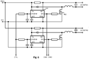
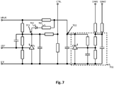
- Figs. 6 and 7 correspond to figs. 4 and 5 and show exemplary circuit diagrams that can be used to implement the functionalities of two output stages ( fig. 6 ) and a common output power limiter ( fig. 7 ).
- the two output stages shown in fig. 6 are identical, so in the following it suffices to give reference designators to components of one of them.
- Each of the two output stages in fig. 6 has the configuration of a switched-mode power supply (in particular: a buck converter) with a switching transistor 402.
- Each of the two output stages comprises a driver circuit 304 for generating switching pulses for the switching transistor 402.
- the driver circuit 304 comprises a current feedback functionality that is configured to act as an output current limiting arrangement, i.e. configured to limit the output current of the respective output stage to an output current value that is smaller than or equal to a current limit value.
- the driver circuit 304 also comprises a dimming input marked as EN/DIM.
- the driver circuit is configured to respond to an analog dimming signal brought to the dimming input by decreasing the current limit value used by the output current limiting arrangement.
- Driver circuits of this kind are commercially available; for example at the time of writing this description the company Monolithic Power Systems (MPS) based in San Jose, California, markets one with the identifier MP24894. The explanations of the pin markings on said driver circuit of MPS are
- a voltage greater than 0.3 V between it and the GND pin turns on the driver circuit, while a voltage rising from 0.3 V to 2.7 V causes the internally applied current limit value to change so that the LED current will change from 20% to 100% of the maximum LED current.
- the voltage range between 0.3 V to 2.7 V may be called the dimming range. If some other driver circuit is used, the dimming range may have some other endpoints.
- the lines labelled DR#1 and DR#2 carry output voltage indicators of the first and second output stages respectively.
- these lines carry voltage waveforms essentially taken from the gate electrode of the respective switching transistors. Under the assumption of constant bus voltage, these voltage waveforms indicate output voltages of the respective output stages.
- the line labelled CTRL is coupled (through a respective resistor) to the EN/DIM pin of each driver circuit 304.
- the components in block 701 are responsible for taking an averaged sum of the output voltage indicators and converting said averaged sum into a value that is inversely proportional to said averaged sum.
- This value is the electric potential of point 702 in the circuit diagram of fig. 7 , or the electric potential difference between it and the 0 V rail.
- a nominal value generation block such as a circuit containing an ISET resistor
- the comparison between the indicator value of point 702 and the nominal value of point 703 takes place with the help of the series connection of a diode 704 and a resistor 705. If the indicator value of point 702 is larger than or equal to the nominal value, the common output power limiter does not need to limit the output power (remembering that the indicator value was inversely proportional to the averaged sum of the output voltage indicators). In this case it is essentially the nominal value at point 703 that goes to the EN/DIM pins of the driver circuits through the CTRL line, with the effect of not decreasing the current limit value from what it is just as a consequence of using a particular ISET resistor.
- the indicator value of point 702 is smaller than the nominal value (by at least the magnitude of the forward voltage drop of diode 704), some of the electric potential of point 703 bleeds out through the diode 704 and resistor 705.
- the voltage that eventually goes to the EN/DIM pins of the driver circuits through the CTRL line constitutes a setpoint value that is somewhere within the dimming range, and has the effect of decreasing the current limit value by an amount that is proportional to the difference between the indicator value and the nominal value.
- the output voltage indicators on lines DR#1 and DR#2 are essentially voltage waveforms taken from the gates of the respective switching transistors.
- An increase in the duty cycle of a switching transistor is by definition an increase of the relative amount of time its gate spends at a high potential. It means an increase in the output voltage of the respective buck converter, and also an increase in the relative amount of time the corresponding output voltage indicator line (the DR#1 line or the DR#2 line) is at high potential.
- An alternative embodiment could be produced, in which the output voltage indicators would be voltage waveforms taken from the drain of each respective switching transistor.
- an increase in the duty cycle of a switching transistor means a decrease in the relative amount of time its drain spends at high potential, so the behavior of an averaged sum of such output voltage indicators as a function of buck converter duty cycles would be a mirror image of that described above.
- the averaged sum could in that case be used as an indicator value as such, without performing an inversion as in fig. 7 .
- one could perform an inversion as in fig. 7 , but the way in which the output power limiter reacts to the indicator value going beyond the nominal value should be redesigned keeping in mind that this time going beyond the nominal value would mean becoming greater than the nominal value.
- Fig. 8 illustrates aspects of a method that can be executed by a driver device for LEDs.
- the various parts of the driver device execute steps of the method simultaneously and without any particular sequential order: a bus voltage is produced with a first converter means having a power rating; output current is provided to one or more light-emitting semiconductor devices through two or more output stages, each coupled to receive said bus voltage and each configured to provide said output current at an output power specific to the respective output stage; and the sum of output powers of said two or more output stages is jointly limited to a combined power value that is smaller than or equal to said power rating.
- Step 801 the method can be thought to begin from forming the switching pulses to the switching transistor according to step 801. Since the output stages receive their operating power from the first converter means, switching pulses can naturally be formed only after the first converter means has begun producing the bus voltage. Steps 802 and 803 correspond to producing an indicator value indicative of the sum of output powers of the two or more output stages. To this end, output voltage indicators are taken from all output stages to summing and averaging in step 802, and the averaged sum is converted further to an indicator value in step 803.
- a nominal value comes from output current setting and corresponds to a desired maximum output current value of each individual output stage when the sum of output powers of said two or more output stages is not jointly limited. Comparing the indicator value to the nominal value takes place at step 804. If the indicator value did not reach or go beyond the nominal value, the setpoint value is formed in step 805 directly from the nominal value. It is possible to use the nominal value directly as the setpoint value, of forming the setpoint value at step 805 may involve some kind of scaling, buffering, or other straightforward processing that aims at bringing the setpoint value to the appropriate input of the driver circuit at the appropriate magnitude; for example, equal to or larger than 2.7 V if a MP24894 type driver circuit is used.
- the method comprises decreasing the current limit value that an output current limiting arrangement in each output stage uses to limit the output current of the respective output stage. This takes place by decreasing the setpoint value from what it would otherwise be, according to step 806, and by taking the setpoint value (which now is between 0.3 V and 2.7 V, if the MP24894 is used) to the appropriate input of the driver circuit.
- Fig. 8 illustrates how the MP24894, which here is used as a non-limiting example of a driver circuit, is internally responsible of generating a lower limit (0.3 V) and an upper limit (2.7 V) and performing a double comparison at step 807. If the voltage between its EN/DIM and GND pins is below the lower limit, the forming of switching pulses is disabled altogether in accordance with step 808. If the voltage is over the upper limit, a current limit value is formed that corresponds to 100% of the desired maximum output current at step 809. A voltage between the upper and lower limits causes the current limit value to be decreased in accordance with step 810 so that the actual output current will be between 20% and 100% of the maximum output current.
- the current feedback functionality of the driver circuit works in a way known as such, by making a comparison at step 811 between a current measurement value and the current limit value, and by limiting the forming of switching pulses in accordance with step 812 if the output current has reached the limit value.
- Fig. 5 assumed that the output current setting was done in a fixed manned by coupling an ISET resistor to a nominal value generating block. Such an approach is frequently used in so-called constant current LED drivers that aim at making the LEDs always shine at constant brightness.
- Fig. 9 illustrates a controllable driver device, in which AC mains voltage is coupled to an input stage 101, which in turn feeds a first converter means 902 that produces a bus voltage and has a power rating. Another input coupling to the driver device of fig. 9 comes through a control bus interface 903.
- Fig. 9 names the control bus a DALI (digital addressable lighting interface) bus, but many other control connections could be used quite as well.
- DALI digital addressable lighting interface
- the control bus interface 903 conveys bidirectional data traffic to and from a processor 904, which has connections to more or less all other functional blocks of the driver device and has overall responsibility of the operation of the driver device.
- the processor 904 may receive dimming commands through the control bus interface 903 and change the brightness of the LEDs coupled to the outputs of the output stages 905 and 906 correspondingly.
- the brightness of the LEDs is changed through PWM (pulse width modulation), which means repeatedly enabling and disabling the operation of the appropriate output stage(s) at a frequency and duty cycle decided by the processor 904.
- the output stages 905 and 906 which are coupled to receive the bus voltage, provide output current to one or more LEDs in pulses, while the pulse frequency (also known as the PWM frequency) is sufficiently high that a human observer only recognizes the produced light as dimmed to a level defined by the PWM duty cycle.
- the PWM signals go through an output power control block 907, which - together with an output current selection block 906 - also implements jointly limiting the sum of output powers of the output stages 905 and 906 to a combined power value that is smaller than or equal to the power rating of the first converter means 902.
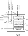
- Fig. 10 shows an example of how the operation of blocks 907 and 908 in fig. 9 can be organized.
- the output voltage indicators from the output stages come to block 1001 for summing and averaging, just like in block 504 of fig. 5 .
- the nominal value is generated in block 1002 on the basis of an ISET value received from the processor; the processor may have a D/A-converter-equipped output for outputting an analog ISET value, or the conversion from digital to analog may be made in the nominal value generation block 1002.
- the driver device comprises a processor in this case, it is possible to alternatively have the output current set simply with an ISET resistor coupled to the nominal value generation block 1002 just like in fig. 5 , instead of receiving an ISET value from the processor.
- the common output power limiter of fig. 10 is configured to produce an indicator value indicative of the sum of output powers of the output stages, and to compare the indicator value to the nominal value in order to find out whether the indicator value goes beyond the nominal value. This takes place in block 1003, just like block 505 of fig. 5 .
- the result of the comparison is a setpoint value that either corresponds directly to the nominal value (in case the indicator value did not go beyond the nominal value) or is changed by an amount proportional to the difference (in case the indicator value went beyond the nominal value). Instead of taking the setpoint value as such to the appropriate control inputs of the driver circuits in the output stages, it is taken through switch 1004 to the first output stage and through switch 1005 to the second output stage.
- the PWM signals from the processor drive the switches 1004 and 1005.
- the corresponding switch is open, which disables the driver circuit in the corresponding output stage regardless of the actual setpoint value.
- the corresponding switch is closed, and the setpoint value is let through to the enabling/dimming input of the corresponding driver circuit.
- the indicator value is directly proportional to the averaged sum of voltage indicators, and going beyond the nominal value is taken as becoming larger than the nominal value.
- Being (directly or inversely) proportional to does not need to mean exact mathematical proportionality, but mainly expresses the fact that is one becomes bigger, the other becomes also bigger (direct proportionality) or the other becomes smaller (inverse proportionality).
Landscapes
- Engineering & Computer Science (AREA)
- Power Engineering (AREA)
- Circuit Arrangement For Electric Light Sources In General (AREA)
Claims (10)
- Treibervorrichtung zum Bereitstellen von Ausgangsstrom für eine oder mehrere lichtemittierende Halbleitervorrichtungen, die Treibervorrichtung umfassend
ein erstes Wandlermittel (102, 902) zum Erzeugen einer Busspannung, wobei das erste Wandlermittel (102, 902) eine Nennleistung aufweist, und
zwei oder mehrere Ausgangsstufen (203, 204, 401, 905, 906), wobei jede gekoppelt ist, um die Busspannung zu empfangen, und jede konfiguriert ist, um Ausgangsstrom mit einer für die jeweiligen Ausgangsstufen spezifischen Ausgangsleistung für eine oder mehrere lichtemittierende Halbleitervorrichtungen, die mit dem Ausgang der jeweiligen Ausgangsstufe gekoppelt sind, bereitzustellen;
dadurch gekennzeichnet, dass die Treibervorrichtung umfasst:
einen gemeinsamen Ausgangsleistungsbegrenzer (201, 501, 907), der konfiguriert ist, um die Summe der Ausgangsleistungen der zwei oder mehreren Ausgangsstufen (203, 204, 401, 905, 906) auf einen kombinierten Leistungswert zu begrenzen, der kleiner oder gleich der Nennleistung ist. - Treibervorrichtung nach Anspruch 1, wobei:jede der zwei oder mehreren Ausgangsstufen (203, 204, 401, 905, 906) eine Ausgangsstrombegrenzungsanordnung (306) umfasst, die konfiguriert ist, um die Ausgangsleistung der jeweiligen Ausgangsstufen auf einen Ausgangsleistungswert zu begrenzen, der kleiner oder gleich eines Stromgrenzwerts ist,der gemeinsame Ausgangsleistungsbegrenzer (201, 501, 907) konfiguriert ist, um einen Indikatorwert zu erzeugen, der die Summe der Ausgangsleistungen der zwei oder mehreren Ausgangsstufen (203, 204, 401, 905, 906) anzeigt, undder gemeinsame Ausgangsleistungsbegrenzer (201, 501, 907) konfiguriert ist, um den Stromgrenzwert zu verringern, der von der Ausgangsstrombegrenzungsanordnung als eine Reaktion auf den Indikatorwert, der einen Nennwert erreicht oder übersteigt, verwendet wird.
- Treibervorrichtung nach Anspruch 2, wobei der gemeinsame Ausgangsleistungsbegrenzer (201, 501, 907) konfiguriert ist, um den Indikatorwert zu produzieren, indem eine Durchschnittssumme der Ausgangsspannungsindikatoren hergenommen wird, die die Ausgangsspannungen der zwei oder mehreren Ausgangsstufen (203, 204, 401, 905, 906) angeben, und die Durchschnittssumme in einen Wert umgewandelt wird, der umgekehrt proportional zur Durchschnittssumme ist.
- Treibervorrichtung nach Anspruch 3, wobei der gemeinsame Ausgangsleistungsbegrenzer (201, 501, 907) konfiguriert ist, um:auf den Indikatorwert, der größer oder gleich dem Nennwert ist, zu reagieren, indem der Stromgrenzwert nicht verringert wird, undauf den Indikatorwert, der kleiner als der Nennwert ist, zu reagieren, indem der Stromgrenzwert um eine Menge, die proportional zur Differenz zwischen dem Indikatorwert und dem Nennwert ist, verringert wird.
- Treibervorrichtung nach einem der Ansprüche 3 oder 4, wobei jede der zwei oder mehreren Ausgangsstufen (203, 204, 401, 905, 906) die Ausgestaltung eines Schaltnetzteils mit einem Schalttransistor (302, 402) aufweist und der gemeinsame Ausgangsleistungsbegrenzer (201, 501, 907) konfiguriert ist, um Spannungsformen, die von einer Elektrode der Schalttransistoren (302, 402) hergenommen sind, als die Ausgangsleistungsindikatoren zu verwenden.
- Treibervorrichtung nach einem der Ansprüche 2 bis 5, wobei:jede der zwei oder mehreren Ausgangsstufen (203, 204, 401, 905, 906) die Ausgestaltung eines Schaltnetzteils mit einem Schalttransistor (302, 402) aufweist,jede der zwei oder mehreren Ausgangsstufen (203, 204, 401, 905, 906) eine Treiberschaltung (304) zum Erzeugen von Schaltimpulsen für den Schalttransistor (302, 402) umfasst,die Treiberschaltung (304) in jeder der zwei oder mehreren Ausgangsstufen (203, 204, 401, 905, 906) eine Stromrückkopplungsfunktionalität umfasst, die konfiguriert ist, um als die Ausgangsstrombegrenzungsanordnung zu fungieren,die Treiberschaltung in jeder der zwei oder mehreren Ausgangsstufen (203, 204, 401, 905, 906) eine Verdunkelungseingabe umfasst und die Treiberschaltung konfiguriert ist, um auf ein analoges Verdunkelungssignal zu reagieren, das zu der Verdunkelungseingabe durch Verringern des Stromgrenzwerts, der von der Ausgangsstrombegrenzungsanordnung verwendet wird, gebracht wurde, undder gemeinsame Ausgangsleistungsbegrenzer (201, 501, 907) konfiguriert ist, um innerhalb eines Verdunkelungsbereichs einen Sollwert zu variieren, der mit der Verdunkelungseingabe als eine Reaktion auf den Indikatorwert, der den Nennwert erreicht oder übersteigt, gekoppelt ist.
- Beleuchtungsanordnung, umfassend
eine Treibervorrichtung nach einem der Ansprüche 1 bis 6, und
Lichtausgabemittel, die elektrisch mit der Treibervorrichtung gekoppelt sind. - Verfahren zum Bereitstellen von Ausgangsstrom für eine oder mehrere lichtemittierende Halbleitervorrichtungen, das Verfahren umfassend
Erzeugen einer Busspannung mit einem ersten Wandelmittel (102, 902), das eine Nennleistung aufweist, und
Bereitstellen von Ausgangsstrom für eine oder mehrere lichtemittierende Halbleitervorrichtungen durch zwei oder mehrere Ausgangsstufen (203, 204, 401, 905, 906), von denen jede gekoppelt ist, um die Busspannung zu empfangen, und jede konfiguriert ist, um den Ausgangsstrom mit einer für die jeweiligen Ausgangsstufen spezifischen Ausgangsleistung breitzustellen;
dadurch gekennzeichnet, dass das Verfahren umfasst:
gemeinsames Begrenzen der Summe von Ausgangsleistungen der zwei oder mehreren Ausgangsstufen (203, 204, 401, 905, 906) auf einen kombinierten Stromwert, der kleiner oder gleich der Nennleistung ist. - Verfahren nach Anspruch 8, wobei der Schritt des gemeinsamen Begrenzens der Summe von Ausgangsleistungen der zwei oder mehreren Ausgangsstufen umfasst:Erzeugen (803) eines Indikatorwerts, der die Summe von Ausgangsleistungen der zwei oder mehreren Ausgangsstufen angibt,Vergleichen (804) des Indikatorwerts mit einem Nennwert, undals eine Reaktion darauf, dass der Indikatorwert den Nennwert erreicht oder übersteigt, Verringern (806) eines Stromgrenzwerts, den eine Ausgangsstrombegrenzungsanordnung in jeder Ausgangsstufe verwendet, um den Ausgangsstrom der jeweiligen Ausgangsstufe zu begrenzen.
- Verfahren nach Anspruch 9, wobei der Nennwert einem gewünschten maximalen Ausgangsstromwert für jede individuelle Ausgangsstufe entspricht, welcher eingestellt wird, ohne einzukalkulieren, dass die Summe der Ausgangsleistungen der zwei oder mehreren Ausgangsstufen gemeinsam begrenzt werden.
Priority Applications (1)
| Application Number | Priority Date | Filing Date | Title |
|---|---|---|---|
| EP14190795.6A EP3016478B1 (de) | 2014-10-29 | 2014-10-29 | Gemeinsame Steuerung der Ausgangsleistung in einem mehrkanaligen LED-Treiber |
Applications Claiming Priority (1)
| Application Number | Priority Date | Filing Date | Title |
|---|---|---|---|
| EP14190795.6A EP3016478B1 (de) | 2014-10-29 | 2014-10-29 | Gemeinsame Steuerung der Ausgangsleistung in einem mehrkanaligen LED-Treiber |
Publications (2)
| Publication Number | Publication Date |
|---|---|
| EP3016478A1 EP3016478A1 (de) | 2016-05-04 |
| EP3016478B1 true EP3016478B1 (de) | 2018-10-03 |
Family
ID=51862123
Family Applications (1)
| Application Number | Title | Priority Date | Filing Date |
|---|---|---|---|
| EP14190795.6A Active EP3016478B1 (de) | 2014-10-29 | 2014-10-29 | Gemeinsame Steuerung der Ausgangsleistung in einem mehrkanaligen LED-Treiber |
Country Status (1)
| Country | Link |
|---|---|
| EP (1) | EP3016478B1 (de) |
Families Citing this family (3)
| Publication number | Priority date | Publication date | Assignee | Title |
|---|---|---|---|---|
| WO2019029798A1 (en) * | 2017-08-09 | 2019-02-14 | HELLA GmbH & Co. KGaA | SYSTEM FOR OPERATING AN ELECTRONIC LIGHT ARRANGEMENT |
| DE102017216902A1 (de) * | 2017-09-25 | 2019-03-28 | Tridonic Gmbh & Co Kg | Vorrichtung und Verfahren zur dynamischen Überlastbegrenzung bei farbtemperaturdimmbaren Mehrkanal-LED-Systemen |
| DE102018115676A1 (de) * | 2018-06-28 | 2020-01-02 | Tridonic Gmbh & Co Kg | Anordnung mit einer Leuchte, insbesondere Notleuchte, mit Farbtemperaturwechsel in einem batteriegestützten Betriebsmodus |
Family Cites Families (2)
| Publication number | Priority date | Publication date | Assignee | Title |
|---|---|---|---|---|
| DE3221873C2 (de) * | 1982-06-09 | 1984-04-26 | Siemens AG, 1000 Berlin und 8000 München | Verfahren und Anordnung zur Reduzierung des Energieverbrauchs einer Bühnenstellanlage |
| US7233115B2 (en) * | 2004-03-15 | 2007-06-19 | Color Kinetics Incorporated | LED-based lighting network power control methods and apparatus |
-
2014
- 2014-10-29 EP EP14190795.6A patent/EP3016478B1/de active Active
Non-Patent Citations (1)
| Title |
|---|
| None * |
Also Published As
| Publication number | Publication date |
|---|---|
| EP3016478A1 (de) | 2016-05-04 |
Similar Documents
| Publication | Publication Date | Title |
|---|---|---|
| JP5981337B2 (ja) | 低コストの電力供給回路及び方法 | |
| CN102461332B (zh) | 用于led组件的控制单元以及照明系统 | |
| US7741788B2 (en) | Light emitting apparatus with current limiting | |
| EP2596680B1 (de) | Triac-dämmsysteme für festkörperlasten | |
| US8816597B2 (en) | LED driving circuit | |
| US9660535B2 (en) | Method and system to dynamically position a switch mode power supply output voltage | |
| CN103052203B (zh) | Led控制电路及其控制方法 | |
| KR20170007735A (ko) | 디밍 장치에서 led 수명 및 색 품질을 향상시키는 방법 및 시스템 | |
| TW201110811A (en) | Adaptive switch mode LED driver | |
| KR20110017784A (ko) | Led 발광 장치 | |
| US10051704B2 (en) | LED dimmer circuit and method | |
| CN109032232B (zh) | 电子装置 | |
| US9210748B2 (en) | Systems and methods of driving multiple outputs | |
| US8441196B2 (en) | Multi-color light emitting device circuit | |
| US20170257916A1 (en) | Lighting device | |
| Lohaus et al. | A dimmable LED driver with resistive DAC feedback control for adaptive voltage regulation | |
| EP3016478B1 (de) | Gemeinsame Steuerung der Ausgangsleistung in einem mehrkanaligen LED-Treiber | |
| EP3043625B1 (de) | Dimmbarer LED-Treiber und Verfahren zur Herstellung eines Dimmsignals | |
| US9408272B2 (en) | Light driver and the controller and driving method thereof | |
| CN106572554B (zh) | 具有对未知输入和负载电压的自动调节的电子控制器 | |
| US9992826B1 (en) | Dual mode constant current LED driver | |
| US11496052B2 (en) | Insulated power supply circuit | |
| EP3370479B1 (de) | Verfahren und schaltung zum schutz von leds von transienten strömen | |
| KR101942494B1 (ko) | 하이브리드 제어 타입의 교류 직접 구동 엘이디 장치 | |
| CN104853486A (zh) | 一种基于pwm的调光电路 |
Legal Events
| Date | Code | Title | Description |
|---|---|---|---|
| PUAI | Public reference made under article 153(3) epc to a published international application that has entered the european phase |
Free format text: ORIGINAL CODE: 0009012 |
|
| AK | Designated contracting states |
Kind code of ref document: A1 Designated state(s): AL AT BE BG CH CY CZ DE DK EE ES FI FR GB GR HR HU IE IS IT LI LT LU LV MC MK MT NL NO PL PT RO RS SE SI SK SM TR |
|
| AX | Request for extension of the european patent |
Extension state: BA ME |
|
| 17P | Request for examination filed |
Effective date: 20161104 |
|
| RBV | Designated contracting states (corrected) |
Designated state(s): AL AT BE BG CH CY CZ DE DK EE ES FI FR GB GR HR HU IE IS IT LI LT LU LV MC MK MT NL NO PL PT RO RS SE SI SK SM TR |
|
| GRAP | Despatch of communication of intention to grant a patent |
Free format text: ORIGINAL CODE: EPIDOSNIGR1 |
|
| RIC1 | Information provided on ipc code assigned before grant |
Ipc: H05B 33/08 20060101AFI20180410BHEP Ipc: H02J 1/10 20060101ALI20180410BHEP Ipc: H02M 3/315 20060101ALI20180410BHEP Ipc: H02M 1/00 20060101ALN20180410BHEP |
|
| INTG | Intention to grant announced |
Effective date: 20180508 |
|
| RIN1 | Information on inventor provided before grant (corrected) |
Inventor name: VILLA, JUHA |
|
| GRAS | Grant fee paid |
Free format text: ORIGINAL CODE: EPIDOSNIGR3 |
|
| GRAA | (expected) grant |
Free format text: ORIGINAL CODE: 0009210 |
|
| AK | Designated contracting states |
Kind code of ref document: B1 Designated state(s): AL AT BE BG CH CY CZ DE DK EE ES FI FR GB GR HR HU IE IS IT LI LT LU LV MC MK MT NL NO PL PT RO RS SE SI SK SM TR |
|
| RAP1 | Party data changed (applicant data changed or rights of an application transferred) |
Owner name: HELVAR OY AB |
|
| REG | Reference to a national code |
Ref country code: GB Ref legal event code: FG4D |
|
| REG | Reference to a national code |
Ref country code: CH Ref legal event code: EP Ref country code: AT Ref legal event code: REF Ref document number: 1050107 Country of ref document: AT Kind code of ref document: T Effective date: 20181015 |
|
| REG | Reference to a national code |
Ref country code: IE Ref legal event code: FG4D Ref country code: DE Ref legal event code: R096 Ref document number: 602014033280 Country of ref document: DE |
|
| REG | Reference to a national code |
Ref country code: NL Ref legal event code: MP Effective date: 20181003 |
|
| REG | Reference to a national code |
Ref country code: LT Ref legal event code: MG4D |
|
| REG | Reference to a national code |
Ref country code: AT Ref legal event code: MK05 Ref document number: 1050107 Country of ref document: AT Kind code of ref document: T Effective date: 20181003 |
|
| PG25 | Lapsed in a contracting state [announced via postgrant information from national office to epo] |
Ref country code: NL Free format text: LAPSE BECAUSE OF FAILURE TO SUBMIT A TRANSLATION OF THE DESCRIPTION OR TO PAY THE FEE WITHIN THE PRESCRIBED TIME-LIMIT Effective date: 20181003 |
|
| PG25 | Lapsed in a contracting state [announced via postgrant information from national office to epo] |
Ref country code: FI Free format text: LAPSE BECAUSE OF FAILURE TO SUBMIT A TRANSLATION OF THE DESCRIPTION OR TO PAY THE FEE WITHIN THE PRESCRIBED TIME-LIMIT Effective date: 20181003 Ref country code: IS Free format text: LAPSE BECAUSE OF FAILURE TO SUBMIT A TRANSLATION OF THE DESCRIPTION OR TO PAY THE FEE WITHIN THE PRESCRIBED TIME-LIMIT Effective date: 20190203 Ref country code: NO Free format text: LAPSE BECAUSE OF FAILURE TO SUBMIT A TRANSLATION OF THE DESCRIPTION OR TO PAY THE FEE WITHIN THE PRESCRIBED TIME-LIMIT Effective date: 20190103 Ref country code: AT Free format text: LAPSE BECAUSE OF FAILURE TO SUBMIT A TRANSLATION OF THE DESCRIPTION OR TO PAY THE FEE WITHIN THE PRESCRIBED TIME-LIMIT Effective date: 20181003 Ref country code: ES Free format text: LAPSE BECAUSE OF FAILURE TO SUBMIT A TRANSLATION OF THE DESCRIPTION OR TO PAY THE FEE WITHIN THE PRESCRIBED TIME-LIMIT Effective date: 20181003 Ref country code: LV Free format text: LAPSE BECAUSE OF FAILURE TO SUBMIT A TRANSLATION OF THE DESCRIPTION OR TO PAY THE FEE WITHIN THE PRESCRIBED TIME-LIMIT Effective date: 20181003 Ref country code: HR Free format text: LAPSE BECAUSE OF FAILURE TO SUBMIT A TRANSLATION OF THE DESCRIPTION OR TO PAY THE FEE WITHIN THE PRESCRIBED TIME-LIMIT Effective date: 20181003 Ref country code: LT Free format text: LAPSE BECAUSE OF FAILURE TO SUBMIT A TRANSLATION OF THE DESCRIPTION OR TO PAY THE FEE WITHIN THE PRESCRIBED TIME-LIMIT Effective date: 20181003 Ref country code: PL Free format text: LAPSE BECAUSE OF FAILURE TO SUBMIT A TRANSLATION OF THE DESCRIPTION OR TO PAY THE FEE WITHIN THE PRESCRIBED TIME-LIMIT Effective date: 20181003 Ref country code: CZ Free format text: LAPSE BECAUSE OF FAILURE TO SUBMIT A TRANSLATION OF THE DESCRIPTION OR TO PAY THE FEE WITHIN THE PRESCRIBED TIME-LIMIT Effective date: 20181003 Ref country code: BG Free format text: LAPSE BECAUSE OF FAILURE TO SUBMIT A TRANSLATION OF THE DESCRIPTION OR TO PAY THE FEE WITHIN THE PRESCRIBED TIME-LIMIT Effective date: 20190103 |
|
| PG25 | Lapsed in a contracting state [announced via postgrant information from national office to epo] |
Ref country code: PT Free format text: LAPSE BECAUSE OF FAILURE TO SUBMIT A TRANSLATION OF THE DESCRIPTION OR TO PAY THE FEE WITHIN THE PRESCRIBED TIME-LIMIT Effective date: 20190203 Ref country code: RS Free format text: LAPSE BECAUSE OF FAILURE TO SUBMIT A TRANSLATION OF THE DESCRIPTION OR TO PAY THE FEE WITHIN THE PRESCRIBED TIME-LIMIT Effective date: 20181003 Ref country code: SE Free format text: LAPSE BECAUSE OF FAILURE TO SUBMIT A TRANSLATION OF THE DESCRIPTION OR TO PAY THE FEE WITHIN THE PRESCRIBED TIME-LIMIT Effective date: 20181003 Ref country code: GR Free format text: LAPSE BECAUSE OF FAILURE TO SUBMIT A TRANSLATION OF THE DESCRIPTION OR TO PAY THE FEE WITHIN THE PRESCRIBED TIME-LIMIT Effective date: 20190104 Ref country code: AL Free format text: LAPSE BECAUSE OF FAILURE TO SUBMIT A TRANSLATION OF THE DESCRIPTION OR TO PAY THE FEE WITHIN THE PRESCRIBED TIME-LIMIT Effective date: 20181003 |
|
| REG | Reference to a national code |
Ref country code: CH Ref legal event code: PL |
|
| REG | Reference to a national code |
Ref country code: BE Ref legal event code: MM Effective date: 20181031 |
|
| PG25 | Lapsed in a contracting state [announced via postgrant information from national office to epo] |
Ref country code: LU Free format text: LAPSE BECAUSE OF NON-PAYMENT OF DUE FEES Effective date: 20181029 |
|
| REG | Reference to a national code |
Ref country code: DE Ref legal event code: R097 Ref document number: 602014033280 Country of ref document: DE |
|
| REG | Reference to a national code |
Ref country code: IE Ref legal event code: MM4A |
|
| PG25 | Lapsed in a contracting state [announced via postgrant information from national office to epo] |
Ref country code: IT Free format text: LAPSE BECAUSE OF FAILURE TO SUBMIT A TRANSLATION OF THE DESCRIPTION OR TO PAY THE FEE WITHIN THE PRESCRIBED TIME-LIMIT Effective date: 20181003 Ref country code: DK Free format text: LAPSE BECAUSE OF FAILURE TO SUBMIT A TRANSLATION OF THE DESCRIPTION OR TO PAY THE FEE WITHIN THE PRESCRIBED TIME-LIMIT Effective date: 20181003 |
|
| PLBE | No opposition filed within time limit |
Free format text: ORIGINAL CODE: 0009261 |
|
| STAA | Information on the status of an ep patent application or granted ep patent |
Free format text: STATUS: NO OPPOSITION FILED WITHIN TIME LIMIT |
|
| PG25 | Lapsed in a contracting state [announced via postgrant information from national office to epo] |
Ref country code: CH Free format text: LAPSE BECAUSE OF NON-PAYMENT OF DUE FEES Effective date: 20181031 Ref country code: MC Free format text: LAPSE BECAUSE OF FAILURE TO SUBMIT A TRANSLATION OF THE DESCRIPTION OR TO PAY THE FEE WITHIN THE PRESCRIBED TIME-LIMIT Effective date: 20181003 Ref country code: SM Free format text: LAPSE BECAUSE OF FAILURE TO SUBMIT A TRANSLATION OF THE DESCRIPTION OR TO PAY THE FEE WITHIN THE PRESCRIBED TIME-LIMIT Effective date: 20181003 Ref country code: EE Free format text: LAPSE BECAUSE OF FAILURE TO SUBMIT A TRANSLATION OF THE DESCRIPTION OR TO PAY THE FEE WITHIN THE PRESCRIBED TIME-LIMIT Effective date: 20181003 Ref country code: RO Free format text: LAPSE BECAUSE OF FAILURE TO SUBMIT A TRANSLATION OF THE DESCRIPTION OR TO PAY THE FEE WITHIN THE PRESCRIBED TIME-LIMIT Effective date: 20181003 Ref country code: SK Free format text: LAPSE BECAUSE OF FAILURE TO SUBMIT A TRANSLATION OF THE DESCRIPTION OR TO PAY THE FEE WITHIN THE PRESCRIBED TIME-LIMIT Effective date: 20181003 Ref country code: LI Free format text: LAPSE BECAUSE OF NON-PAYMENT OF DUE FEES Effective date: 20181031 Ref country code: BE Free format text: LAPSE BECAUSE OF NON-PAYMENT OF DUE FEES Effective date: 20181031 |
|
| 26N | No opposition filed |
Effective date: 20190704 |
|
| GBPC | Gb: european patent ceased through non-payment of renewal fee |
Effective date: 20190103 |
|
| PG25 | Lapsed in a contracting state [announced via postgrant information from national office to epo] |
Ref country code: IE Free format text: LAPSE BECAUSE OF NON-PAYMENT OF DUE FEES Effective date: 20181029 Ref country code: FR Free format text: LAPSE BECAUSE OF NON-PAYMENT OF DUE FEES Effective date: 20181203 Ref country code: SI Free format text: LAPSE BECAUSE OF FAILURE TO SUBMIT A TRANSLATION OF THE DESCRIPTION OR TO PAY THE FEE WITHIN THE PRESCRIBED TIME-LIMIT Effective date: 20181003 |
|
| REG | Reference to a national code |
Ref country code: DE Ref legal event code: R079 Ref document number: 602014033280 Country of ref document: DE Free format text: PREVIOUS MAIN CLASS: H05B0033080000 Ipc: H05B0045000000 |
|
| PG25 | Lapsed in a contracting state [announced via postgrant information from national office to epo] |
Ref country code: GB Free format text: LAPSE BECAUSE OF NON-PAYMENT OF DUE FEES Effective date: 20190103 |
|
| PG25 | Lapsed in a contracting state [announced via postgrant information from national office to epo] |
Ref country code: MT Free format text: LAPSE BECAUSE OF NON-PAYMENT OF DUE FEES Effective date: 20181029 |
|
| PG25 | Lapsed in a contracting state [announced via postgrant information from national office to epo] |
Ref country code: TR Free format text: LAPSE BECAUSE OF FAILURE TO SUBMIT A TRANSLATION OF THE DESCRIPTION OR TO PAY THE FEE WITHIN THE PRESCRIBED TIME-LIMIT Effective date: 20181003 |
|
| PG25 | Lapsed in a contracting state [announced via postgrant information from national office to epo] |
Ref country code: HU Free format text: LAPSE BECAUSE OF FAILURE TO SUBMIT A TRANSLATION OF THE DESCRIPTION OR TO PAY THE FEE WITHIN THE PRESCRIBED TIME-LIMIT; INVALID AB INITIO Effective date: 20141029 Ref country code: CY Free format text: LAPSE BECAUSE OF FAILURE TO SUBMIT A TRANSLATION OF THE DESCRIPTION OR TO PAY THE FEE WITHIN THE PRESCRIBED TIME-LIMIT Effective date: 20181003 Ref country code: MK Free format text: LAPSE BECAUSE OF NON-PAYMENT OF DUE FEES Effective date: 20181003 |
|
| PGFP | Annual fee paid to national office [announced via postgrant information from national office to epo] |
Ref country code: DE Payment date: 20231027 Year of fee payment: 10 |