EP3012867A1 - Semiconductor devices and methods of manufacturing semiconductor devices - Google Patents
Semiconductor devices and methods of manufacturing semiconductor devices Download PDFInfo
- Publication number
- EP3012867A1 EP3012867A1 EP15190765.6A EP15190765A EP3012867A1 EP 3012867 A1 EP3012867 A1 EP 3012867A1 EP 15190765 A EP15190765 A EP 15190765A EP 3012867 A1 EP3012867 A1 EP 3012867A1
- Authority
- EP
- European Patent Office
- Prior art keywords
- metal oxide
- layer
- insulating interlayer
- disposed
- oxide layer
- Prior art date
- Legal status (The legal status is an assumption and is not a legal conclusion. Google has not performed a legal analysis and makes no representation as to the accuracy of the status listed.)
- Granted
Links
Images



Classifications
-
- H—ELECTRICITY
- H10—SEMICONDUCTOR DEVICES; ELECTRIC SOLID-STATE DEVICES NOT OTHERWISE PROVIDED FOR
- H10D—INORGANIC ELECTRIC SEMICONDUCTOR DEVICES
- H10D30/00—Field-effect transistors [FET]
- H10D30/60—Insulated-gate field-effect transistors [IGFET]
- H10D30/67—Thin-film transistors [TFT]
- H10D30/674—Thin-film transistors [TFT] characterised by the active materials
- H10D30/6755—Oxide semiconductors, e.g. zinc oxide, copper aluminium oxide or cadmium stannate
-
- H—ELECTRICITY
- H10—SEMICONDUCTOR DEVICES; ELECTRIC SOLID-STATE DEVICES NOT OTHERWISE PROVIDED FOR
- H10D—INORGANIC ELECTRIC SEMICONDUCTOR DEVICES
- H10D30/00—Field-effect transistors [FET]
- H10D30/01—Manufacture or treatment
- H10D30/021—Manufacture or treatment of FETs having insulated gates [IGFET]
- H10D30/031—Manufacture or treatment of FETs having insulated gates [IGFET] of thin-film transistors [TFT]
-
- H—ELECTRICITY
- H10—SEMICONDUCTOR DEVICES; ELECTRIC SOLID-STATE DEVICES NOT OTHERWISE PROVIDED FOR
- H10D—INORGANIC ELECTRIC SEMICONDUCTOR DEVICES
- H10D30/00—Field-effect transistors [FET]
- H10D30/60—Insulated-gate field-effect transistors [IGFET]
- H10D30/67—Thin-film transistors [TFT]
- H10D30/6704—Thin-film transistors [TFT] having supplementary regions or layers in the thin films or in the insulated bulk substrates for controlling properties of the device
-
- H—ELECTRICITY
- H10—SEMICONDUCTOR DEVICES; ELECTRIC SOLID-STATE DEVICES NOT OTHERWISE PROVIDED FOR
- H10D—INORGANIC ELECTRIC SEMICONDUCTOR DEVICES
- H10D30/00—Field-effect transistors [FET]
- H10D30/60—Insulated-gate field-effect transistors [IGFET]
- H10D30/67—Thin-film transistors [TFT]
- H10D30/6704—Thin-film transistors [TFT] having supplementary regions or layers in the thin films or in the insulated bulk substrates for controlling properties of the device
- H10D30/6713—Thin-film transistors [TFT] having supplementary regions or layers in the thin films or in the insulated bulk substrates for controlling properties of the device characterised by the properties of the source or drain regions, e.g. compositions or sectional shapes
-
- H—ELECTRICITY
- H10—SEMICONDUCTOR DEVICES; ELECTRIC SOLID-STATE DEVICES NOT OTHERWISE PROVIDED FOR
- H10D—INORGANIC ELECTRIC SEMICONDUCTOR DEVICES
- H10D30/00—Field-effect transistors [FET]
- H10D30/60—Insulated-gate field-effect transistors [IGFET]
- H10D30/67—Thin-film transistors [TFT]
- H10D30/6729—Thin-film transistors [TFT] characterised by the electrodes
- H10D30/673—Thin-film transistors [TFT] characterised by the electrodes characterised by the shapes, relative sizes or dispositions of the gate electrodes
-
- H—ELECTRICITY
- H10—SEMICONDUCTOR DEVICES; ELECTRIC SOLID-STATE DEVICES NOT OTHERWISE PROVIDED FOR
- H10D—INORGANIC ELECTRIC SEMICONDUCTOR DEVICES
- H10D64/00—Electrodes of devices having potential barriers
- H10D64/01—Manufacture or treatment
- H10D64/011—Manufacture or treatment of electrodes ohmically coupled to a semiconductor
-
- H—ELECTRICITY
- H10—SEMICONDUCTOR DEVICES; ELECTRIC SOLID-STATE DEVICES NOT OTHERWISE PROVIDED FOR
- H10D—INORGANIC ELECTRIC SEMICONDUCTOR DEVICES
- H10D86/00—Integrated devices formed in or on insulating or conducting substrates, e.g. formed in silicon-on-insulator [SOI] substrates or on stainless steel or glass substrates
- H10D86/40—Integrated devices formed in or on insulating or conducting substrates, e.g. formed in silicon-on-insulator [SOI] substrates or on stainless steel or glass substrates characterised by multiple TFTs
- H10D86/451—Integrated devices formed in or on insulating or conducting substrates, e.g. formed in silicon-on-insulator [SOI] substrates or on stainless steel or glass substrates characterised by multiple TFTs characterised by the compositions or shapes of the interlayer dielectrics
-
- H—ELECTRICITY
- H10—SEMICONDUCTOR DEVICES; ELECTRIC SOLID-STATE DEVICES NOT OTHERWISE PROVIDED FOR
- H10D—INORGANIC ELECTRIC SEMICONDUCTOR DEVICES
- H10D86/00—Integrated devices formed in or on insulating or conducting substrates, e.g. formed in silicon-on-insulator [SOI] substrates or on stainless steel or glass substrates
- H10D86/40—Integrated devices formed in or on insulating or conducting substrates, e.g. formed in silicon-on-insulator [SOI] substrates or on stainless steel or glass substrates characterised by multiple TFTs
- H10D86/60—Integrated devices formed in or on insulating or conducting substrates, e.g. formed in silicon-on-insulator [SOI] substrates or on stainless steel or glass substrates characterised by multiple TFTs wherein the TFTs are in active matrices
-
- H—ELECTRICITY
- H10—SEMICONDUCTOR DEVICES; ELECTRIC SOLID-STATE DEVICES NOT OTHERWISE PROVIDED FOR
- H10D—INORGANIC ELECTRIC SEMICONDUCTOR DEVICES
- H10D99/00—Subject matter not provided for in other groups of this subclass
-
- H—ELECTRICITY
- H10—SEMICONDUCTOR DEVICES; ELECTRIC SOLID-STATE DEVICES NOT OTHERWISE PROVIDED FOR
- H10P—GENERIC PROCESSES OR APPARATUS FOR THE MANUFACTURE OR TREATMENT OF DEVICES COVERED BY CLASS H10
- H10P14/00—Formation of materials, e.g. in the shape of layers or pillars
- H10P14/60—Formation of materials, e.g. in the shape of layers or pillars of insulating materials
- H10P14/63—Formation of materials, e.g. in the shape of layers or pillars of insulating materials characterised by the formation processes
- H10P14/6302—Non-deposition formation processes
- H10P14/6304—Formation by oxidation, e.g. oxidation of the substrate
- H10P14/6314—Formation by oxidation, e.g. oxidation of the substrate of a metallic layer
-
- H—ELECTRICITY
- H10—SEMICONDUCTOR DEVICES; ELECTRIC SOLID-STATE DEVICES NOT OTHERWISE PROVIDED FOR
- H10P—GENERIC PROCESSES OR APPARATUS FOR THE MANUFACTURE OR TREATMENT OF DEVICES COVERED BY CLASS H10
- H10P14/00—Formation of materials, e.g. in the shape of layers or pillars
- H10P14/60—Formation of materials, e.g. in the shape of layers or pillars of insulating materials
- H10P14/63—Formation of materials, e.g. in the shape of layers or pillars of insulating materials characterised by the formation processes
- H10P14/6302—Non-deposition formation processes
- H10P14/6322—Formation by thermal treatments
Definitions
- the present invention relates to semiconductor devices and methods of manufacturing semiconductor devices. More particularly, the present invention relate to oxide semiconductor devices including protection structures, and methods of manufacturing the oxide semiconductor devices including the protection structures.
- a conventional thin film transistor (“TFT”) having a bottom gate configuration generally includes a gate electrode disposed on a substrate, a gate insulation layer disposed on the gate insulation layer, a source electrode and a drain electrode disposed on the gate insulation layer, and an active layer among the gate insulation layer, the source electrode, and the drain electrode.
- the source electrode and the drain electrode may make contact with a source region and a drain region of the active layer.
- the conventional transistor having a bottom gate configuration moisture and/or hydrogen may be permeated into the structures of the transistor such that the electrical characteristics of the transistor may be easily degraded.
- variation of the threshold voltage (Vth) of the transistor may be caused by moisture and/or hydrogen, so that the transistor may have degraded electrical characteristics, such as an increase of the threshold voltage distribution, a decrease of the driving current, etc.
- the conventional oxide semiconductor device which includes an active layer of oxide semiconductor, may be relatively sensitive to moisture and/or hydrogen, and thus, the electrical characteristics of the oxide semiconductor device may be easily degraded.
- Such a degraded oxide semiconductor device may not be properly employed in recent display devices, such as liquid crystal display devices, organic light emitting display devices, etc.
- Exemplary embodiments of the present invention provide oxide semiconductor devices having improved electrical characteristics by preventing permeation of moisture and/or hydrogen.
- Exemplary embodiments of the present invention also provide methods of manufacturing oxide semiconductor devices having improved electrical characteristics by prevention permeation of moisture and/or hydrogen.
- An exemplary embodiment of the present invention discloses a semiconductor device including: a gate electrode disposed on a substrate, a gate insulation layer disposed on the substrate to cover the gate electrode, an active layer including an oxide semiconductor disposed on the gate insulation layer, an insulating interlayer disposed on the gate insulation layer and covering the active layer, a protection structure disposed on the insulating interlayer, and a source electrode and a drain electrode disposed on the protection structure.
- the protection structure may include a plurality of metal oxide layers.
- the source electrode and the drain electrode may contact a source region and a drain region of the active layer, respectively.
- An exemplary embodiment of the present invention also discloses a semiconductor device including: a gate electrode disposed on a substrate, a gate insulation layer disposed on the substrate and covering the gate electrode, an active layer disposed on the gate insulation layer, the active layer including an oxide semiconductor, a first insulating interlayer disposed on the gate insulation layer and covering the active layer, a source electrode and a drain electrode disposed on the first insulating interlayer, a second insulating interlayer disposed on the first insulating interlayer, the source electrode and the drain electrode, and a protection structure disposed on the second insulating interlayer.
- the protection structure may include a plurality of metal oxide layers.
- the source electrode and the drain electrode may contact a source region and a drain region of the active layer, respectively.
- An exemplary embodiment of the present invention also discloses a method of manufacturing a semiconductor device.
- a gate electrode may be formed on a substrate, and a gate insulation layer may be formed on the substrate to cover the gate electrode.
- an insulating interlayer may be formed on the active layer to substantially cover the gate insulation layer.
- a protection structure including a plurality of metal oxide layers may be formed on the insulating interlayer.
- a source electrode and a drain electrode may be formed on the protection structure. The source electrode and the drain electrode may contact a source region and a drain region of the active layer, respectively.
- An exemplary embodiment of the present invention also discloses a method of manufacturing a semiconductor device.
- a gate electrode may be formed on a substrate.
- a gate insulation layer may be formed on the substrate to substantially cover the gate electrode.
- An active layer including an oxide semiconductor may be formed on the gate insulation layer, and then a first insulating interlayer may be formed on the active layer to substantially cover the gate insulation layer.
- a source electrode and a drain electrode may be formed on the first insulating interlayer. The source electrode and the drain electrode may contact a source region and a drain region of the active layer, respectively.
- a second first insulating interlayer may be formed on the first insulating interlayer, the source electrode and the drain electrode, and then a protection structure including a plurality of metal oxide layers may be formed on the second insulating interlayer.
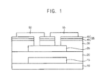
- FIG. 1 is a cross-sectional view illustrating an oxide semiconductor device in accordance with an exemplary embodiment.
- a semiconductor device may include a gate electrode 15, a gate insulation layer 20, an active layer 25, an insulating interlayer 30, a protection structure 35, a source electrode 50, and a drain electrode 55, which may be sequentially disposed on a substrate 10.
- the protection structure 35 may include a plurality of metal oxide layers.
- the protection structure 35 may include a first metal oxide layer 40 and a second metal oxide layer 45.
- each of the first metal oxide layer 40 and the second metal oxide layer 45 may include aluminium oxide (AlOx), titanium oxide (TiOx), tantalum oxide (TaOx), zirconium oxide (ZrOx), etc.
- the substrate 10 may include an insulation material.
- the substrate 10 may include a glass substrate, a transparent plastic substrate, a transparent metal oxide substrate, etc.
- at least one buffer layer may be provided on the substrate 10.
- the buffer layer may include silicon oxide (SiOx), silicon nitride (SiNx), silicon oxynitride (SiOxNy), etc.
- the gate electrode 15 may be provided on the substrate 10.
- the oxide semiconductor device illustrated in FIG. 1 may have a bottom gate configuration. However, the oxide semiconductor device may have various other configurations, for example, a top gate configuration, a dual gate configuration, etc.
- the gate electrode 15 may include a metal, an alloy, a metal nitride, a conductive metal oxide, a transparent conductive material, etc.
- the gate electrode 15 may include aluminium (Al), an alloy containing aluminium, aluminium nitride (AlNx), silver (Ag), an alloy containing silver, tungsten (W), tungsten nitride (WNx), copper (Cu), an alloy containing copper, nickel (Ni), chrome (Cr), molybdenum (Mo), an alloy containing molybdenum, titanium (Ti), titanium nitride (TiNx), platinum (Pt), tantalum (Ta), tantalum nitride (TaNx), neodymium (Nd), scandium (Sc), strontium ruthenium oxide (SrRuxOy), zinc oxide (ZnOx), indium tin oxide (ITO), tin oxide (SnOx), gallium oxide (GaOx), indium
- the gate insulation layer 20 may be disposed on the substrate 10 to substantially cover the gate electrode 15.
- the gate insulation layer 20 may sufficiently cover the gate electrode 15, and have a substantially level surface without a step around the gate electrode 15.
- the gate insulation layer 20 may include silicon compound, metal oxide, etc.
- the gate insulation layer 20 may include silicon oxide, silicon nitride, silicon oxynitride, aluminium oxide, tantalum oxide, hafnium oxide, zirconium oxide, titanium oxide, etc. These may be used alone or in a combination thereof.
- the active layer 25 may be located on the gate insulation layer 20.
- the active layer 25 may include a semiconductor oxide, such as binary system compound (ABx), ternary system compound (ABxCy) or quaternary system compound (ABxCyDz), which may contain indium, zinc, gallium, tin, titanium, aluminium, hafnium (Hf), zirconium (Zr), magnesium (Mg), etc.
- ABx binary system compound
- ABxCy ternary system compound
- ABSDz quaternary system compound
- the active layer 25 may include indium-gallium-zinc oxide (IGZO), gallium zinc oxide (GaZnxOy), indium tin oxide (ITO), indium zinc oxide (IZO), zinc magnesium oxide (ZnMgxOy), zinc tin oxide (ZnSnxOy), zinc zirconium oxide (ZnZRxOy), zinc oxide (ZnOx), gallium oxide (GaOx), titanium oxide (TiOx), tin oxide (SnOx), indium oxide (InOx), indium-gallium-hafnium oxide (IGHO), tin-aluminium-zinc oxide (TAZO), indium-gallium-tin oxide (IGSO), etc. These may be used alone or in a mixture thereof.
- IGZO indium-gallium-zinc oxide
- GaZnxOy gallium zinc oxide
- ITO indium zinc oxide
- IZO zinc magnesium oxide
- ZnMgxOy zinc tin
- the insulating interlayer 30 may be provided on the gate insulation layer 20 to substantially cover the active layer 25.
- the insulating interlayer 30 may sufficiently cover the active layer 25 while having a substantially flat upper face without a step around the active layer 25.
- the insulating interlayer 30 may include silicon compound.
- the insulating interlayer 30 may include silicon oxide, silicon nitride, silicon oxynitride, etc. These may be used alone or in a combination thereof.
- the protection structure 35 may be disposed on the insulating interlayer 30.
- the protection structure 35 may include the first metal oxide layer 40 disposed on the insulating interlayer 30, and the second metal oxide layer 45 disposed on the first metal oxide layer 40.
- the first metal oxide layer 40 may include a metal oxide substantially the same as that contained in the second metal oxide layer 45.
- each of the first and the second metal oxide layers 40 and 45 may include aluminium oxide, titanium oxide, tantalum oxide, zirconium oxide, etc. These may be used alone or in a combination thereof.
- the first and the second metal oxide layers 40 and 45 may have different oxygen contents, respectively.
- the first metal oxide layer 40 may have a first composition of MOx1 (wherein, M represents aluminium, titanium, tantalum or zirconium, O denotes oxygen, and x means a positive real number) that may contain a first metal oxide having a first oxygen content.
- the second metal oxide layer 45 may have a second composition of MOx2 that may contain a second metal oxide having a second oxygen content.
- the first metal oxide layer 40 may have the first composition of AlOx1 containing aluminium oxide having the first oxygen content
- the second metal oxide layer 45 may have the second composition of AlOx2 containing aluminium oxide having the second oxygen content.
- the first oxygen content of the first metal oxide layer 40 may be substantially greater than the second oxygen content of the second metal oxide layer 45.
- a difference between the first oxygen content and the second oxygen content may be more than 3 atomic percentage (at%).
- the first metal oxide layer 40 may have a thickness between about 5nm (50 ⁇ ) and about 100nm (1,000 ⁇ )
- the second metal oxide layer 45 may have a thickness of about 3nm (30 ⁇ ) to about 30nm (300 ⁇ ).
- a thickness ratio between the first metal oxide layer 40 and the second metal oxide layer 45 may be in a range of about 1.0: 0.03 to about 1.0: 0.6.
- the second oxygen content of the second metal oxide layer 45 may be substantially greater than the first oxygen content of the first metal oxide layer 40.
- the second oxygen content may be higher than the first oxygen content by more than 3 at%.
- the thickness of the first metal oxide layer 40 may be in a range between about 3nm (30 ⁇ ) and about 30nm (300 ⁇ ) while the thickness of the second metal oxide layer 45 may be in a range between about 5nm (50 ⁇ ) and about 100nm (1,000 ⁇ ).
- the second oxygen content may be abruptly varied from the first oxygen content at an interface between the first metal oxide layer 40 and the second metal oxide layer 45.
- the second oxygen content may be suddenly increased or decreased from the first oxygen content at an interface between the first metal oxide layer 40 and the second metal oxide layer 45.
- the protection structure 35 may prevent the underlying structures from external moisture and/or hydrogen. If moisture and/or hydrogen permeate into the underlying structure of the oxide semiconductor device, the concentration of charge carriers in the active layer 25 may be undesirably increased and, thus, the threshold voltage (Vth) of the oxide semiconductor device may be negatively shifted, thereby degrading the electrical characteristics of the oxide semiconductor device.
- Vth threshold voltage
- the oxide semiconductor device may ensure improved electrical characteristics by preventing the threshold voltage shift thereof.
- the source electrode 50 and the drain electrode 55 may be provided on the second metal oxide layer 45 of the protection structure 35.
- the source and the drain electrodes 50 and 55 may pass through the protection structure 35 and the insulating interlayer 30 so that the source and the drain electrodes 50 and 55 may make contact with a source region and a drain region of the active layer 25.
- a source contact hole and drain contact hole may be provided through the protection structure 35 and the insulating interlayer 30.
- the source and the drain contact holes may expose the source and the drain regions of the active layer 25, respectively.
- Each of the source and the drain regions 50 and 55 may include a metal, an alloy, a metal nitride, a conductive metal oxide, a transparent conductive material, etc.
- each of the source and the drain electrodes 50 and 55 may include aluminium, copper, molybdenum, titanium, chrome, tantalum, tungsten, neodymium, scandium, alloys thereof, nitrides thereof, strontium ruthenium oxide, indium tin oxide, indium zinc oxide, zinc oxide, tin oxide, carbon nanotube, etc.
- FIG. 2 is a flow chart illustrating a method of manufacturing an oxide semiconductor device in accordance with an exemplary embodiment.
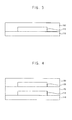
- FIGS. 3 to 6 are cross-sectional views illustrating a method of manufacturing an oxide semiconductor device in accordance with an exemplary embodiment.
- a gate electrode 115 may be formed on a substrate 110, which may be composed of transparent material, such as glass, transparent plastic, transparent ceramic, etc.
- the gate electrode 115 may be formed by a sputtering process, a spray process, a chemical vapor deposition (CVD) process, an atomic layer deposition (ALD) process, a vacuum evaporation process, a printing process, etc.
- the gate electrode 115 may be obtained using metal such as aluminium, tungsten, copper, nickel, chrome, molybdenum, titanium, platinum, tantalum or ruthenium, alloy containing these metals, nitrides of these metals, or conductive metal oxide.
- a gate insulation layer 120 may be formed on the substrate 110 to cover the gate electrodes 115 in step S120.
- the gate insulation layer 120 may be formed by a CVD process, a thermal oxidation process, a plasma enhanced chemical vapor deposition (PECVD) process, a high density plasma-chemical vapor deposition (HDP-CVD) process, etc.
- the gate insulation layer 120 may be formed using silicon compound, metal oxide, etc.
- the gate insulation layer 120 may have a relatively large thickness that may sufficiently cover the gate electrode 115 on the substrate 110.
- an active layer 125 may be formed on the gate insulation layer 120 in step S130.
- the active layer 125 may be obtained by a sputtering process, a CVD process, a printing process, a vacuum evaporation process, an ALD process, a sol-gel process, a PECVD process, etc.
- the active layer 125 may be formed using a semiconductor oxide, such as a binary system compound, a ternary system compound, or a quaternary system compound.
- the active layer 125 may be formed using a semiconductor oxide containing indium, gallium, tin, titanium, aluminium, hafnium, zirconium, magnesium, etc.
- the active layer 125 may be disposed on a portion of the gate insulation layer 120 under which the gate electrode 115 is disposed.
- An insulating interlayer 130 may be formed on the gate insulation layer 120 to substantially cover the active layer 125 in step of S140.
- the insulating interlayer 130 may have a substantially flat upper face that sufficiently covers the active layer 125.
- a planarization process may be performed on the insulating interlayer 130 such that the insulating interlayer 130 may have such a level surface.
- a first metal oxide layer 140 may be formed on the insulating interlayer 130 in step S150.
- the first metal oxide layer 140 may be formed by a sputtering process, a PECVD process, a CVD process, a vacuum evaporation process, etc. Additionally, the first metal oxide layer 140 may be formed using aluminium oxide, titanium oxide, tantalum oxide, zirconium oxide, etc.
- a gas mixture including an inactive gas e.g., an argon (Ar) gas, a neon (Ne) gas, a nitrogen (N2) gas, etc.
- an oxygen (O 2 ) gas may be introduced into a chamber having a substantial vacuum pressure, and then the gas mixture may changed into a plasma containing oxygen to thereby provide an atmosphere containing oxygen in the chamber.
- an inactive gas e.g., an argon (Ar) gas, a neon (Ne) gas, a nitrogen (N2) gas, etc.
- oxygen (O 2 ) gas may be introduced into a chamber having a substantial vacuum pressure, and then the gas mixture may changed into a plasma containing oxygen to thereby provide an atmosphere containing oxygen in the chamber.
- the first metal oxide layer 140 may be formed on the insulating interlayer 130.
- a metal layer (not illustrated) may be formed on the first metal oxide layer 140.
- the metal layer may be formed by a sputtering process using a target containing aluminium, titanium, tantalum or zirconium under an atmosphere containing no oxygen.
- An oxidation treatment may be performed on the metal layer so that a second metal oxide layer 145 may be formed on the first metal oxide layer 140 in step S160.
- a protection structure 135, which may include a plurality of metal oxide layers such as the first and the second metal oxide layers 140 and 145, may be provided on the insulating interlayer 135.
- the protection structure 135 may prevent moisture and/or hydrogen from permeating into the resultant structures, such that the protection structure 135 may enhance the electrical characteristics of the oxide semiconductor device by preventing the variation of threshold voltage (Vth) of the oxide semiconductor device.
- the protection structure 135 of the metal oxide may have a relative large area when the protection structure 135 may include the plurality of metal oxide layers (e.g., 140 and 145) having different oxygen contents, respectively.
- the first metal oxide layer 140 and/or the second metal oxide layer 145 may have a relatively large area when each of the first and the second metal oxide layers 140 and 145 includes aluminium oxide by the processes described above.
- the second metal oxide layer 145 may be obtained by forming the metal layer on the first metal oxide layer 140 under the atmosphere including no oxygen, and then by performing a thermal treatment on the metal layer under an atmosphere containing oxygen.
- the second metal oxide layer 145 may be obtained by an annealing process performed at a temperature of about 200°C to about 500°C.
- the first metal oxide layer 140 may have a first oxygen content different from a second oxygen content of the second metal oxide layer 145.
- the first metal oxide layer 140 may have a first metal oxide composition of MOx1 having the first oxygen content
- the second metal oxide layer 145 may have a metal oxide second composition of MOx2 having the second oxygen content.
- the second oxygen content of the second metal oxide layer 145 may abruptly vary from the first oxygen content of the first metal oxide layer 140.
- the first oxygen content of the first metal oxide layer 140 may be greater than the second oxygen content of the second metal oxide layer 145 by more than about 3 at%.
- the second oxygen content may abruptly decrease from the second oxygen content at an interface between the first metal oxide layer 140 and the second metal oxide layer 145.
- a difference between the first oxygen content and the second oxygen content in the protection structure 135 may be achieved by controlling process conditions such as temperatures and/or concentrations of oxygen in the process for forming the first metal oxide layer 140 and/or the thermal treatment for forming the second metal oxide layer 145.
- the second oxygen content of the second metal oxide layer 145 may be greater than the first oxygen content of the first metal oxide layer 140 by more than about 3 at%.
- the second oxygen content may abruptly increase from the second oxygen content at the interface between the first metal oxide layer 140 and the second metal oxide layer 145.
- the second metal oxide layer 145, the first metal oxide layer 140, and the insulating interlayer 130 may be partially removed to form a source contact hole 131 and a drain contact hole 133 in step S170.
- the source contact hole 131 and the drain contact hole 133 may expose a source region and a drain region of the active layer 125, respectively.
- a source electrode (not illustrated) and a drain electrode (not illustrated) may be formed on the second metal oxide layer 145 while filling the source contact hole 131 and the drain contact hole 133, respectively.
- the oxide semiconductor device having a configuration substantially the same as that of the oxide semiconductor device described with reference to FIG. 1 .
- the source and the drain electrodes may be formed by a CVD process, a vacuum evaporation process, a sputtering process, a PECVD process, an ALD process, etc. Further, each of the source and the drain electrodes may be formed using a metal, an alloy, a metal nitride, a conductive metal oxide, a transparent conductive material, etc.
- FIG. 7 is a cross-sectional view illustrating an oxide semiconductor device in accordance with another exemplary embodiment.
- the oxide semiconductor device may include a gate electrode 215, a gate insulation layer 220, an active layer 225, a first insulating interlayer 230, a source electrode 250, a drain electrode 255, a second insulating interlayer 260, a protection structure 265, etc.
- the protection structure 265 may include a plurality of metal oxide layers such as a first metal oxide layer 270 and a second metal oxide layer 275.
- the first and the second metal oxide layers 270 and 275 may include aluminium oxide, titanium oxide, tantalum oxide, zirconium oxide, etc.
- the gate electrode 215 may be provided on a substrate 210 including hard transparent material or soft transparent material.
- the gate electrode 215 may include a metal, an alloy, a metal nitride, a conductive metal oxide, a transparent conductive material, etc.
- the gate insulation layer 220 covering the gate electrode 215 may be disposed on the substrate 210.
- the gate insulation layer 220 may include a silicon compound, a metal oxide, etc.
- the active layer 225 may be disposed on the gate insulation layer 220.
- the active layer 225 may include semiconductor oxide containing a binary system compound, a ternary system compound, a quaternary system compound, etc.
- the first insulating interlayer 230 may locate on the gate insulation layer 220 while substantially covering the active layer 225.
- the first insulating interlayer 230 may include silicon compound.
- the source and the drain electrodes 250 and 255 may be disposed on the first insulating interlayer 230.
- the source electrode 250 and the drain electrode 255 may pass through a source contact hole and a drain contact hole formed through the insulating interlayer 230, and then may make contact with a source region and a drain region of the active layer 225.
- Each of the source and the drain regions 250 and 255 may include a metal, an alloy, a metal nitride, a conductive metal oxide, a transparent conductive material, etc.
- the source and the drain electrodes 250 and 255 may include aluminium, copper, molybdenum, titanium, chrome, tantalum, tungsten, neodymium, scandium, alloys thereof, nitrides thereof, strontium ruthenium oxide, indium tin oxide, indium zinc oxide, zinc oxide, tin oxide, carbon nanotube, etc.
- the second insulating interlayer 260 may be disposed on the first insulating interlayer 230 to substantially cover the source electrode 250 and the drain electrode 255.
- the second insulating interlayer 260 may have a substantially flat upper face while sufficiently covering the source and the drain electrodes 250 and 255.
- the protection structure 265 may be positioned the second insulating interlayer 260.
- the protection structure 265 may have the first and the second metal oxide layers 270 and 275 sequentially disposed on the second insulating interlayer 260.
- the first and the second metal oxide layers 270 and 275 may include the same metal oxide whereas the first metal oxide layer 270 may have an oxygen content different from that of the second metal oxide layer 275.
- the first metal oxide layer 270 may have a first composition of MOx1 (M indicates metal such as aluminium, titanium, tantalum or zirconium, O means oxygen and x represents a positive real number) containing a first oxygen content while the second metal oxide layer 275 may have a second composition of MOx2 containing a second oxygen content.
- the first metal oxide layer 270 may have the first composition of AlOx1 including the first oxygen content
- the second metal oxide layer 275 may have the second composition of AlOx2 including the second oxygen content.
- the first oxygen content of the first metal oxide layer 270 may be greater than the second oxygen content of the second metal oxide layer 275.
- an oxygen content difference between the first metal oxide layer 270 and the second metal oxide layer 275 may be more than about 3 at%.
- the first metal oxide layer 270 may have a thickness of about 5nm (50 ⁇ ) to about 100nm (1,000 ⁇ )
- the second metal oxide layer 275 may have a thickness of about 3nm (30 ⁇ ) to about 30nm (300 ⁇ ).
- a thickness ratio between the first and the second metal oxide layers 270 and 275 may be in a range between about 1.0: 0.03 and about 1.0: 0.6.
- the second oxygen content of the second metal oxide layer 275 may be greater than the first oxygen content of the first metal oxide layer 270.
- the second oxygen content may be greater than the first oxygen content by more than about 3 at%.
- the first metal oxide layer 270 may have a thickness of about 3nm (30 ⁇ ) to about 30nm (300 ⁇ ), and the second metal oxide layer 275 may have a thickness of about 5nm (50 ⁇ ) to about 100nm (1,000 ⁇ ).
- the first oxygen content of the first metal oxide layer 270 may be substantially greater or less than the second oxygen content of the second metal oxide layer 275.
- the variation from the first oxygen content to the second oxygen content may not be gradual but abrupt.
- the second oxygen content may be abruptly changed from the first oxygen content at an interface between the first and the second metal oxide layers 270 and 275.
- the protection structure 265 having the first and the second metal oxide layers 270 and 275 may effectively block the permeation of moisture and/or hydrogen from an outside, so that the variation of the threshold voltage (Vth) of the oxide semiconductor device may be substantially prevented.
- Vth threshold voltage
- the charge carrier density of the active layer 225 may increase such that the threshold voltage of the oxide semiconductor device may negatively shift, resulting in the deterioration of the electrical characteristics of the oxide semiconductor device.
- the protection structure 265 may prevent the moisture and/or hydrogen from being permeated into the oxide semiconductor device as described above, and thus, the electrical characteristics of the oxide semiconductor device may be enhanced.
- FIG. 8 is a flow chart illustrating a method of manufacturing an oxide semiconductor device in accordance with an exemplary embodiment.
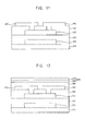
- FIGS. 9 to 12 are cross-sectional views illustrating a method of manufacturing an oxide semiconductor device in accordance with an exemplary embodiment.
- a gate electrode 315 may be formed on a substrate 310 including insulation material in step S 210.
- the gate electrode 315 may be formed by a sputtering process, a CVD process, an ALD process, a vacuum evaporation process or a printing process using a metal, an alloy, a metal nitride, a conductive metal oxide, etc.
- a gate insulation layer 320 may be formed on the substrate 310 to substantially cover the gate electrode 315.
- the gate insulation layer 320 may be formed by a CVD process, a thermal oxidation process, a PECVD process or an HDP-CVD process using a silicon compound, a metal oxide, etc.
- an active layer 325 may be formed on the gate insulation layer 320 in step S230.
- the active layer 325 may be obtained by a sputtering process, a CVD process, a printing process, a spray process, a sol-gel process, a vacuum evaporation process, an ALD process, a PECVD process, etc. Further, the active layer 325 may be formed using oxide semiconductor containing indium, zinc, gallium, tin, titanium, aluminium, hafnium, zirconium, magnesium, etc.
- a first insulating interlayer 330 may be formed on the gate insulation layer 320 to substantially cover the active layer 325 in step S240.
- the first insulating interlayer 330 may sufficiently cover the active layer 325 and have a substantially level surface.
- the first insulating interlayer 330 may be formed using silicon compound by a CVD process, a PECVD process, an HDP-CVD process, etc.
- the first insulating interlayer 330 may be partially etched to provide a source contact hole and a drain contact hole which may expose portions of the active layer 325.
- the source contact hole and the drain contact hole may expose a source region and a drain region of the active layer 325, respectively.
- a source electrode 350 and a drain electrode 355 may be formed on the active layer 325 and the first insulating interlayer 330.
- the source and the drain electrodes 350 and 355 may fill the source and the drain contact holes, respectively. Hence, the source and the drain electrodes 350 and 355 may make contact with the source and the drain regions of the active layer 325.
- a second insulating interlayer 360 may be formed on the first insulating interlayer 330 in step S270.
- the second insulating interlayer 360 may sufficiently cover the source and the drain electrodes 350 and 355, and may have a substantially flat upper face.
- the second insulating interlayer 360 may be formed using a material substantially the same as that for the first insulating interlayer 330.
- the second insulating interlayer 360 may be formed using an organic material.
- a protection structure 375 may be formed on the second insulating interlayer 360.
- a first metal oxide layer 365 may be formed on the second insulating interlayer 360n in step S280.
- the first metal oxide layer 365 may be formed using aluminium oxide, titanium oxide, tantalum oxide or zirconium oxide by a sputtering process, a vacuum evaporation process, a CVD process, etc.
- the first metal oxide layer 365 may have a first composition of MOx1 having a first oxygen content.
- a second metal oxide layer 370 may be formed on the first metal oxide layer 365 in step S290.
- a metal layer (not illustrated) may be formed on the first metal oxide layer 365, and then the metal oxide layer may be oxidized to obtain the second metal oxide layer 370.
- the metal layer may be formed using aluminium, titanium, tantalum, zirconium, etc.
- an oxidation treatment for the metal layer may include a thermal oxidation process such as an annealing process performed under an atmosphere containing oxygen.
- the second metal oxide layer 370 may have a second composition of MOx2 having a second oxygen content which may be less than or greater than the first oxygen content.
- the protection structure 375 may prevent the permeation of the moisture and/or hydrogen from an outside, so the oxide semiconductor device may ensure improved electrical characteristics by blocking the variation of the threshold voltage thereof. Further, the metal oxide layers 365 and 360 of the protection structure 375 may be formed to have relatively large areas by the above described processes.
- the oxide semiconductor device including the above-described protection structure when applied to a display device such as an organic light emitting display device or a liquid crystal display device, the display device may also ensure improved quality of image displayed thereon, am enhanced response speed, etc.
- the protection structure including the plurality of metal oxide layers may effectively block the permeation of moisture and/or hydrogen from an outside, so that the electrical characteristics of the oxide semiconductor device may not be substantially deteriorated by the moisture and/or hydrogen. Further, when a display device includes the oxide semiconductor device including the protection structure, the display device may also have improved image quality, enhanced response speed, etc.
Landscapes
- Thin Film Transistor (AREA)
Abstract
Description
- The present invention relates to semiconductor devices and methods of manufacturing semiconductor devices. More particularly, the present invention relate to oxide semiconductor devices including protection structures, and methods of manufacturing the oxide semiconductor devices including the protection structures.
- A conventional thin film transistor ("TFT") having a bottom gate configuration generally includes a gate electrode disposed on a substrate, a gate insulation layer disposed on the gate insulation layer, a source electrode and a drain electrode disposed on the gate insulation layer, and an active layer among the gate insulation layer, the source electrode, and the drain electrode. The source electrode and the drain electrode may make contact with a source region and a drain region of the active layer.
- In the formation of the conventional transistor having a bottom gate configuration, moisture and/or hydrogen may be permeated into the structures of the transistor such that the electrical characteristics of the transistor may be easily degraded. For example, variation of the threshold voltage (Vth) of the transistor may be caused by moisture and/or hydrogen, so that the transistor may have degraded electrical characteristics, such as an increase of the threshold voltage distribution, a decrease of the driving current, etc. In particular, the conventional oxide semiconductor device, which includes an active layer of oxide semiconductor, may be relatively sensitive to moisture and/or hydrogen, and thus, the electrical characteristics of the oxide semiconductor device may be easily degraded. Such a degraded oxide semiconductor device may not be properly employed in recent display devices, such as liquid crystal display devices, organic light emitting display devices, etc.
- Exemplary embodiments of the present invention provide oxide semiconductor devices having improved electrical characteristics by preventing permeation of moisture and/or hydrogen.
- Exemplary embodiments of the present invention also provide methods of manufacturing oxide semiconductor devices having improved electrical characteristics by prevention permeation of moisture and/or hydrogen.
- Additional aspects will be set forth in the detailed description which follows, and, in part, will be apparent from the disclosure, or may be learned by practice of the inventive concept.
- An exemplary embodiment of the present invention discloses a semiconductor device including: a gate electrode disposed on a substrate, a gate insulation layer disposed on the substrate to cover the gate electrode, an active layer including an oxide semiconductor disposed on the gate insulation layer, an insulating interlayer disposed on the gate insulation layer and covering the active layer, a protection structure disposed on the insulating interlayer, and a source electrode and a drain electrode disposed on the protection structure. The protection structure may include a plurality of metal oxide layers. The source electrode and the drain electrode may contact a source region and a drain region of the active layer, respectively.
- An exemplary embodiment of the present invention also discloses a semiconductor device including: a gate electrode disposed on a substrate, a gate insulation layer disposed on the substrate and covering the gate electrode, an active layer disposed on the gate insulation layer, the active layer including an oxide semiconductor, a first insulating interlayer disposed on the gate insulation layer and covering the active layer, a source electrode and a drain electrode disposed on the first insulating interlayer, a second insulating interlayer disposed on the first insulating interlayer, the source electrode and the drain electrode, and a protection structure disposed on the second insulating interlayer. The protection structure may include a plurality of metal oxide layers. The source electrode and the drain electrode may contact a source region and a drain region of the active layer, respectively.
- An exemplary embodiment of the present invention also discloses a method of manufacturing a semiconductor device. In the method of manufacturing the semiconductor device, a gate electrode may be formed on a substrate, and a gate insulation layer may be formed on the substrate to cover the gate electrode. After forming an active layer including an oxide semiconductor on the gate insulation layer, an insulating interlayer may be formed on the active layer to substantially cover the gate insulation layer. A protection structure including a plurality of metal oxide layers may be formed on the insulating interlayer. A source electrode and a drain electrode may be formed on the protection structure. The source electrode and the drain electrode may contact a source region and a drain region of the active layer, respectively.
- An exemplary embodiment of the present invention also discloses a method of manufacturing a semiconductor device. In the method of manufacturing the semiconductor device, a gate electrode may be formed on a substrate. A gate insulation layer may be formed on the substrate to substantially cover the gate electrode. An active layer including an oxide semiconductor may be formed on the gate insulation layer, and then a first insulating interlayer may be formed on the active layer to substantially cover the gate insulation layer. A source electrode and a drain electrode may be formed on the first insulating interlayer. The source electrode and the drain electrode may contact a source region and a drain region of the active layer, respectively. A second first insulating interlayer may be formed on the first insulating interlayer, the source electrode and the drain electrode, and then a protection structure including a plurality of metal oxide layers may be formed on the second insulating interlayer.
- The foregoing general description and the following detailed description are exemplary and explanatory and are intended to provide further explanation of the claimed subject matter.
- The accompanying drawings, which are included to provide a further understanding of the inventive concept, and are incorporated in and constitute a part of this specification, illustrate exemplary embodiments of the inventive concept, and, together with the description, serve to explain principles of the inventive concept.
-
FIG. 1 is a cross-sectional view illustrating an oxide semiconductor device in accordance with an exemplary embodiment. -
FIG. 2 is a flow chart illustrating a method of manufacturing an oxide semiconductor device in accordance with an exemplary embodiment. -
FIG. 3, FIG. 4 ,FIG. 5, and FIG. 6 are cross-sectional views illustrating a method of manufacturing an oxide semiconductor device in accordance with an exemplary embodiment. -
FIG. 7 is a cross-sectional view illustrating an oxide semiconductor device in accordance with an exemplary embodiment. -
FIG. 8 is a flow chart illustrating a method of manufacturing an oxide semiconductor device in accordance with an exemplary embodiment. -
FIG. 9, FIG. 10 ,FIG. 11, and FIG. 12 are cross-sectional views illustrating a method of manufacturing an oxide semiconductor device in accordance with an exemplary embodiment. - In the following description, for the purposes of explanation, numerous specific details are set forth in order to provide a thorough understanding of various exemplary embodiments. It is apparent, however, that various exemplary embodiments may be practiced without these specific details or with one or more equivalent arrangements. In other instances, well-known structures and devices are shown in block diagram form in order to avoid unnecessarily obscuring various exemplary embodiments.
- In the accompanying figures, the size and relative sizes of layers, films, panels, regions, etc., may be exaggerated for clarity and descriptive purposes. Also, like reference numerals denote like elements.
-
FIG. 1 is a cross-sectional view illustrating an oxide semiconductor device in accordance with an exemplary embodiment. - Referring to
FIG. 1 , a semiconductor device may include agate electrode 15, agate insulation layer 20, anactive layer 25, aninsulating interlayer 30, aprotection structure 35, asource electrode 50, and adrain electrode 55, which may be sequentially disposed on asubstrate 10. Theprotection structure 35 may include a plurality of metal oxide layers. For example, theprotection structure 35 may include a first metal oxide layer 40 and a secondmetal oxide layer 45. Here, each of the first metal oxide layer 40 and the secondmetal oxide layer 45 may include aluminium oxide (AlOx), titanium oxide (TiOx), tantalum oxide (TaOx), zirconium oxide (ZrOx), etc. - The
substrate 10 may include an insulation material. For example, thesubstrate 10 may include a glass substrate, a transparent plastic substrate, a transparent metal oxide substrate, etc. Although not illustrated, at least one buffer layer may be provided on thesubstrate 10. For example, the buffer layer may include silicon oxide (SiOx), silicon nitride (SiNx), silicon oxynitride (SiOxNy), etc. - The
gate electrode 15 may be provided on thesubstrate 10. The oxide semiconductor device illustrated inFIG. 1 may have a bottom gate configuration. However, the oxide semiconductor device may have various other configurations, for example, a top gate configuration, a dual gate configuration, etc. - The
gate electrode 15 may include a metal, an alloy, a metal nitride, a conductive metal oxide, a transparent conductive material, etc. For example, thegate electrode 15 may include aluminium (Al), an alloy containing aluminium, aluminium nitride (AlNx), silver (Ag), an alloy containing silver, tungsten (W), tungsten nitride (WNx), copper (Cu), an alloy containing copper, nickel (Ni), chrome (Cr), molybdenum (Mo), an alloy containing molybdenum, titanium (Ti), titanium nitride (TiNx), platinum (Pt), tantalum (Ta), tantalum nitride (TaNx), neodymium (Nd), scandium (Sc), strontium ruthenium oxide (SrRuxOy), zinc oxide (ZnOx), indium tin oxide (ITO), tin oxide (SnOx), gallium oxide (GaOx), indium zinc Oxide (IZO), etc. These may be used alone or in a combination thereof. - The
gate insulation layer 20 may be disposed on thesubstrate 10 to substantially cover thegate electrode 15. In an exemplary embodiment, thegate insulation layer 20 may sufficiently cover thegate electrode 15, and have a substantially level surface without a step around thegate electrode 15. Thegate insulation layer 20 may include silicon compound, metal oxide, etc. For example, thegate insulation layer 20 may include silicon oxide, silicon nitride, silicon oxynitride, aluminium oxide, tantalum oxide, hafnium oxide, zirconium oxide, titanium oxide, etc. These may be used alone or in a combination thereof. - As illustrated in
FIG. 1 , theactive layer 25 may be located on thegate insulation layer 20. Theactive layer 25 may include a semiconductor oxide, such as binary system compound (ABx), ternary system compound (ABxCy) or quaternary system compound (ABxCyDz), which may contain indium, zinc, gallium, tin, titanium, aluminium, hafnium (Hf), zirconium (Zr), magnesium (Mg), etc. For example, theactive layer 25 may include indium-gallium-zinc oxide (IGZO), gallium zinc oxide (GaZnxOy), indium tin oxide (ITO), indium zinc oxide (IZO), zinc magnesium oxide (ZnMgxOy), zinc tin oxide (ZnSnxOy), zinc zirconium oxide (ZnZRxOy), zinc oxide (ZnOx), gallium oxide (GaOx), titanium oxide (TiOx), tin oxide (SnOx), indium oxide (InOx), indium-gallium-hafnium oxide (IGHO), tin-aluminium-zinc oxide (TAZO), indium-gallium-tin oxide (IGSO), etc. These may be used alone or in a mixture thereof. - The insulating
interlayer 30 may be provided on thegate insulation layer 20 to substantially cover theactive layer 25. In an exemplary embodiment, the insulatinginterlayer 30 may sufficiently cover theactive layer 25 while having a substantially flat upper face without a step around theactive layer 25. The insulatinginterlayer 30 may include silicon compound. For example, the insulatinginterlayer 30 may include silicon oxide, silicon nitride, silicon oxynitride, etc. These may be used alone or in a combination thereof. - The
protection structure 35 may be disposed on the insulatinginterlayer 30. Theprotection structure 35 may include the first metal oxide layer 40 disposed on the insulatinginterlayer 30, and the secondmetal oxide layer 45 disposed on the first metal oxide layer 40. In an exemplary embodiment, the first metal oxide layer 40 may include a metal oxide substantially the same as that contained in the secondmetal oxide layer 45. For example, each of the first and the second metal oxide layers 40 and 45 may include aluminium oxide, titanium oxide, tantalum oxide, zirconium oxide, etc. These may be used alone or in a combination thereof. - According to an exemplary embodiment, the first and the second metal oxide layers 40 and 45 may have different oxygen contents, respectively. The first metal oxide layer 40 may have a first composition of MOx1 (wherein, M represents aluminium, titanium, tantalum or zirconium, O denotes oxygen, and x means a positive real number) that may contain a first metal oxide having a first oxygen content. Additionally, the second
metal oxide layer 45 may have a second composition of MOx2 that may contain a second metal oxide having a second oxygen content. For example, in case that the first and the second metal oxide layers 40 an 45 include aluminium, the first metal oxide layer 40 may have the first composition of AlOx1 containing aluminium oxide having the first oxygen content, and the secondmetal oxide layer 45 may have the second composition of AlOx2 containing aluminium oxide having the second oxygen content. - In an exemplary embodiment, the first oxygen content of the first metal oxide layer 40 may be substantially greater than the second oxygen content of the second
metal oxide layer 45. For example, a difference between the first oxygen content and the second oxygen content may be more than 3 atomic percentage (at%). In this case, the first metal oxide layer 40 may have a thickness between about 5nm (50Å) and about 100nm (1,000Å), and the secondmetal oxide layer 45 may have a thickness of about 3nm (30Å) to about 30nm (300Å). Accordingly, a thickness ratio between the first metal oxide layer 40 and the secondmetal oxide layer 45 may be in a range of about 1.0: 0.03 to about 1.0: 0.6. - In an exemplary embodiment, the second oxygen content of the second
metal oxide layer 45 may be substantially greater than the first oxygen content of the first metal oxide layer 40. For example, the second oxygen content may be higher than the first oxygen content by more than 3 at%. Here, the thickness of the first metal oxide layer 40 may be in a range between about 3nm (30Å) and about 30nm (300Å) while the thickness of the secondmetal oxide layer 45 may be in a range between about 5nm (50Å) and about 100nm (1,000Å). - Regarding the first and the second metal oxide layers 40 and 45 described above, the second oxygen content may be abruptly varied from the first oxygen content at an interface between the first metal oxide layer 40 and the second
metal oxide layer 45. For example, the second oxygen content may be suddenly increased or decreased from the first oxygen content at an interface between the first metal oxide layer 40 and the secondmetal oxide layer 45. - According to an exemplary embodiment, the
protection structure 35, including the first and the second metal oxide layers 40 and 45, may prevent the underlying structures from external moisture and/or hydrogen. If moisture and/or hydrogen permeate into the underlying structure of the oxide semiconductor device, the concentration of charge carriers in theactive layer 25 may be undesirably increased and, thus, the threshold voltage (Vth) of the oxide semiconductor device may be negatively shifted, thereby degrading the electrical characteristics of the oxide semiconductor device. When theprotection structure 35 blocks the permeation of moisture and/or hydrogen from an outside, the oxide semiconductor device may ensure improved electrical characteristics by preventing the threshold voltage shift thereof. - The
source electrode 50 and thedrain electrode 55 may be provided on the secondmetal oxide layer 45 of theprotection structure 35. The source and thedrain electrodes protection structure 35 and the insulatinginterlayer 30 so that the source and thedrain electrodes active layer 25. In an exemplary embodiment, a source contact hole and drain contact hole may be provided through theprotection structure 35 and the insulatinginterlayer 30. The source and the drain contact holes may expose the source and the drain regions of theactive layer 25, respectively. When the source and thedrain electrodes drain electrodes drain regions drain electrodes -
FIG. 2 is a flow chart illustrating a method of manufacturing an oxide semiconductor device in accordance with an exemplary embodiment.FIGS. 3 to 6 are cross-sectional views illustrating a method of manufacturing an oxide semiconductor device in accordance with an exemplary embodiment. - Referring to
FIGS. 2 and3 , in step S110, agate electrode 115 may be formed on asubstrate 110, which may be composed of transparent material, such as glass, transparent plastic, transparent ceramic, etc. Thegate electrode 115 may be formed by a sputtering process, a spray process, a chemical vapor deposition (CVD) process, an atomic layer deposition (ALD) process, a vacuum evaporation process, a printing process, etc. Thegate electrode 115 may be obtained using metal such as aluminium, tungsten, copper, nickel, chrome, molybdenum, titanium, platinum, tantalum or ruthenium, alloy containing these metals, nitrides of these metals, or conductive metal oxide. - A
gate insulation layer 120 may be formed on thesubstrate 110 to cover thegate electrodes 115 in step S120. Thegate insulation layer 120 may be formed by a CVD process, a thermal oxidation process, a plasma enhanced chemical vapor deposition (PECVD) process, a high density plasma-chemical vapor deposition (HDP-CVD) process, etc. Thegate insulation layer 120 may be formed using silicon compound, metal oxide, etc. Thegate insulation layer 120 may have a relatively large thickness that may sufficiently cover thegate electrode 115 on thesubstrate 110. - Referring to
FIGS. 2 and4 , anactive layer 125 may be formed on thegate insulation layer 120 in step S130. Theactive layer 125 may be obtained by a sputtering process, a CVD process, a printing process, a vacuum evaporation process, an ALD process, a sol-gel process, a PECVD process, etc. Theactive layer 125 may be formed using a semiconductor oxide, such as a binary system compound, a ternary system compound, or a quaternary system compound. For example, theactive layer 125 may be formed using a semiconductor oxide containing indium, gallium, tin, titanium, aluminium, hafnium, zirconium, magnesium, etc. Theactive layer 125 may be disposed on a portion of thegate insulation layer 120 under which thegate electrode 115 is disposed. - An insulating
interlayer 130 may be formed on thegate insulation layer 120 to substantially cover theactive layer 125 in step of S140. The insulatinginterlayer 130 may have a substantially flat upper face that sufficiently covers theactive layer 125. In an exemplary embodiment, a planarization process may be performed on the insulatinginterlayer 130 such that the insulatinginterlayer 130 may have such a level surface. - Referring to
FIGS. 2 and5 , a first metal oxide layer 140 may be formed on the insulatinginterlayer 130 in step S150. The first metal oxide layer 140 may be formed by a sputtering process, a PECVD process, a CVD process, a vacuum evaporation process, etc. Additionally, the first metal oxide layer 140 may be formed using aluminium oxide, titanium oxide, tantalum oxide, zirconium oxide, etc. - In the formation of the first metal oxide layer 140 according to an exemplary embodiment, a gas mixture including an inactive gas (e.g., an argon (Ar) gas, a neon (Ne) gas, a nitrogen (N2) gas, etc.) and an oxygen (O2) gas may be introduced into a chamber having a substantial vacuum pressure, and then the gas mixture may changed into a plasma containing oxygen to thereby provide an atmosphere containing oxygen in the chamber. When a sputtering process using a target containing aluminium, titanium, tantalum or zirconium is performed under the atmosphere containing oxygen, the first metal oxide layer 140 may be formed on the insulating
interlayer 130. - In an exemplary embodiment, a metal layer (not illustrated) may be formed on the first metal oxide layer 140. The metal layer may be formed by a sputtering process using a target containing aluminium, titanium, tantalum or zirconium under an atmosphere containing no oxygen. An oxidation treatment may be performed on the metal layer so that a second
metal oxide layer 145 may be formed on the first metal oxide layer 140 in step S160. As a result, aprotection structure 135, which may include a plurality of metal oxide layers such as the first and the secondmetal oxide layers 140 and 145, may be provided on the insulatinginterlayer 135. Theprotection structure 135 may prevent moisture and/or hydrogen from permeating into the resultant structures, such that theprotection structure 135 may enhance the electrical characteristics of the oxide semiconductor device by preventing the variation of threshold voltage (Vth) of the oxide semiconductor device. Moreover, theprotection structure 135 of the metal oxide may have a relative large area when theprotection structure 135 may include the plurality of metal oxide layers (e.g., 140 and 145) having different oxygen contents, respectively. For example, the first metal oxide layer 140 and/or the secondmetal oxide layer 145 may have a relatively large area when each of the first and the secondmetal oxide layers 140 and 145 includes aluminium oxide by the processes described above. - In an exemplary embodiment, the second
metal oxide layer 145 may be obtained by forming the metal layer on the first metal oxide layer 140 under the atmosphere including no oxygen, and then by performing a thermal treatment on the metal layer under an atmosphere containing oxygen. For example, the secondmetal oxide layer 145 may be obtained by an annealing process performed at a temperature of about 200°C to about 500°C. - According to an exemplary embodiment, the first metal oxide layer 140 may have a first oxygen content different from a second oxygen content of the second
metal oxide layer 145. The first metal oxide layer 140 may have a first metal oxide composition of MOx1 having the first oxygen content, and the secondmetal oxide layer 145 may have a metal oxide second composition of MOx2 having the second oxygen content. The second oxygen content of the secondmetal oxide layer 145 may abruptly vary from the first oxygen content of the first metal oxide layer 140. In some Exemplary embodiments, the first oxygen content of the first metal oxide layer 140 may be greater than the second oxygen content of the secondmetal oxide layer 145 by more than about 3 at%. Here, the second oxygen content may abruptly decrease from the second oxygen content at an interface between the first metal oxide layer 140 and the secondmetal oxide layer 145. A difference between the first oxygen content and the second oxygen content in theprotection structure 135 may be achieved by controlling process conditions such as temperatures and/or concentrations of oxygen in the process for forming the first metal oxide layer 140 and/or the thermal treatment for forming the secondmetal oxide layer 145. In other exemplary embodiments, the second oxygen content of the secondmetal oxide layer 145 may be greater than the first oxygen content of the first metal oxide layer 140 by more than about 3 at%. Here, the second oxygen content may abruptly increase from the second oxygen content at the interface between the first metal oxide layer 140 and the secondmetal oxide layer 145. - Referring to
FIGS. 2 and6 , the secondmetal oxide layer 145, the first metal oxide layer 140, and the insulatinginterlayer 130 may be partially removed to form asource contact hole 131 and adrain contact hole 133 in step S170. Thesource contact hole 131 and thedrain contact hole 133 may expose a source region and a drain region of theactive layer 125, respectively. - In step S180, a source electrode (not illustrated) and a drain electrode (not illustrated) may be formed on the second
metal oxide layer 145 while filling thesource contact hole 131 and thedrain contact hole 133, respectively. Accordingly, there is provided the oxide semiconductor device having a configuration substantially the same as that of the oxide semiconductor device described with reference toFIG. 1 . The source and the drain electrodes may be formed by a CVD process, a vacuum evaporation process, a sputtering process, a PECVD process, an ALD process, etc. Further, each of the source and the drain electrodes may be formed using a metal, an alloy, a metal nitride, a conductive metal oxide, a transparent conductive material, etc. -
FIG. 7 is a cross-sectional view illustrating an oxide semiconductor device in accordance with another exemplary embodiment. - Referring to
FIG. 7 , the oxide semiconductor device may include agate electrode 215, agate insulation layer 220, anactive layer 225, a first insulatinginterlayer 230, asource electrode 250, adrain electrode 255, a second insulatinginterlayer 260, a protection structure 265, etc. The protection structure 265 may include a plurality of metal oxide layers such as a first metal oxide layer 270 and a second metal oxide layer 275. For example, the first and the second metal oxide layers 270 and 275 may include aluminium oxide, titanium oxide, tantalum oxide, zirconium oxide, etc. - The
gate electrode 215 may be provided on asubstrate 210 including hard transparent material or soft transparent material. Thegate electrode 215 may include a metal, an alloy, a metal nitride, a conductive metal oxide, a transparent conductive material, etc. Thegate insulation layer 220 covering thegate electrode 215 may be disposed on thesubstrate 210. Thegate insulation layer 220 may include a silicon compound, a metal oxide, etc. Further, theactive layer 225 may be disposed on thegate insulation layer 220. Theactive layer 225 may include semiconductor oxide containing a binary system compound, a ternary system compound, a quaternary system compound, etc. - The first insulating
interlayer 230 may locate on thegate insulation layer 220 while substantially covering theactive layer 225. The first insulatinginterlayer 230 may include silicon compound. The source and thedrain electrodes interlayer 230. Thesource electrode 250 and thedrain electrode 255 may pass through a source contact hole and a drain contact hole formed through the insulatinginterlayer 230, and then may make contact with a source region and a drain region of theactive layer 225. Each of the source and thedrain regions drain electrodes - As illustrated in
FIG. 7 , the second insulatinginterlayer 260 may be disposed on the first insulatinginterlayer 230 to substantially cover thesource electrode 250 and thedrain electrode 255. The secondinsulating interlayer 260 may have a substantially flat upper face while sufficiently covering the source and thedrain electrodes - The protection structure 265 may be positioned the second insulating
interlayer 260. The protection structure 265 may have the first and the second metal oxide layers 270 and 275 sequentially disposed on the second insulatinginterlayer 260. The first and the second metal oxide layers 270 and 275 may include the same metal oxide whereas the first metal oxide layer 270 may have an oxygen content different from that of the second metal oxide layer 275. For example, the first metal oxide layer 270 may have a first composition of MOx1 (M indicates metal such as aluminium, titanium, tantalum or zirconium, O means oxygen and x represents a positive real number) containing a first oxygen content while the second metal oxide layer 275 may have a second composition of MOx2 containing a second oxygen content. When the first and the second metal oxide layers 270 and 275 includes aluminium oxide, the first metal oxide layer 270 may have the first composition of AlOx1 including the first oxygen content, and the second metal oxide layer 275 may have the second composition of AlOx2 including the second oxygen content. - In an exemplary embodiment, the first oxygen content of the first metal oxide layer 270 may be greater than the second oxygen content of the second metal oxide layer 275. For example, an oxygen content difference between the first metal oxide layer 270 and the second metal oxide layer 275 may be more than about 3 at%. In this case, the first metal oxide layer 270 may have a thickness of about 5nm (50Å) to about 100nm (1,000Å), and the second metal oxide layer 275 may have a thickness of about 3nm (30Å) to about 30nm (300Å). Thus, a thickness ratio between the first and the second metal oxide layers 270 and 275 may be in a range between about 1.0: 0.03 and about 1.0: 0.6.
- In another exemplary embodiment, the second oxygen content of the second metal oxide layer 275 may be greater than the first oxygen content of the first metal oxide layer 270. For example, the second oxygen content may be greater than the first oxygen content by more than about 3 at%. In this case, the first metal oxide layer 270 may have a thickness of about 3nm (30Å) to about 30nm (300Å), and the second metal oxide layer 275 may have a thickness of about 5nm (50Å) to about 100nm (1,000Å).
- As described above, the first oxygen content of the first metal oxide layer 270 may be substantially greater or less than the second oxygen content of the second metal oxide layer 275. The variation from the first oxygen content to the second oxygen content may not be gradual but abrupt. For example, the second oxygen content may be abruptly changed from the first oxygen content at an interface between the first and the second metal oxide layers 270 and 275.
- According to an exemplary embodiment, the protection structure 265 having the first and the second metal oxide layers 270 and 275 may effectively block the permeation of moisture and/or hydrogen from an outside, so that the variation of the threshold voltage (Vth) of the oxide semiconductor device may be substantially prevented. When the moisture or hydrogen passes through the oxide semiconductor device, the charge carrier density of the
active layer 225 may increase such that the threshold voltage of the oxide semiconductor device may negatively shift, resulting in the deterioration of the electrical characteristics of the oxide semiconductor device. However, the protection structure 265 may prevent the moisture and/or hydrogen from being permeated into the oxide semiconductor device as described above, and thus, the electrical characteristics of the oxide semiconductor device may be enhanced. -
FIG. 8 is a flow chart illustrating a method of manufacturing an oxide semiconductor device in accordance with an exemplary embodiment.FIGS. 9 to 12 are cross-sectional views illustrating a method of manufacturing an oxide semiconductor device in accordance with an exemplary embodiment. - Referring to
FIGS. 8 and9 , agate electrode 315 may be formed on asubstrate 310 including insulation material instep S 210. Thegate electrode 315 may be formed by a sputtering process, a CVD process, an ALD process, a vacuum evaporation process or a printing process using a metal, an alloy, a metal nitride, a conductive metal oxide, etc. - In step S220, a
gate insulation layer 320 may be formed on thesubstrate 310 to substantially cover thegate electrode 315. Thegate insulation layer 320 may be formed by a CVD process, a thermal oxidation process, a PECVD process or an HDP-CVD process using a silicon compound, a metal oxide, etc. - Referring to
FIGS. 8 and10 , anactive layer 325 may be formed on thegate insulation layer 320 in step S230. Theactive layer 325 may be obtained by a sputtering process, a CVD process, a printing process, a spray process, a sol-gel process, a vacuum evaporation process, an ALD process, a PECVD process, etc. Further, theactive layer 325 may be formed using oxide semiconductor containing indium, zinc, gallium, tin, titanium, aluminium, hafnium, zirconium, magnesium, etc. - A first insulating
interlayer 330 may be formed on thegate insulation layer 320 to substantially cover theactive layer 325 in step S240. The first insulatinginterlayer 330 may sufficiently cover theactive layer 325 and have a substantially level surface. The first insulatinginterlayer 330 may be formed using silicon compound by a CVD process, a PECVD process, an HDP-CVD process, etc. - Referring to
FIGS. 8 and11 , in step S250, the first insulatinginterlayer 330 may be partially etched to provide a source contact hole and a drain contact hole which may expose portions of theactive layer 325. The source contact hole and the drain contact hole may expose a source region and a drain region of theactive layer 325, respectively. - In step S260, a
source electrode 350 and adrain electrode 355 may be formed on theactive layer 325 and the first insulatinginterlayer 330. The source and thedrain electrodes drain electrodes active layer 325. - Referring to
FIGS. 8 and12 , a second insulatinginterlayer 360 may be formed on the first insulatinginterlayer 330 in step S270. The secondinsulating interlayer 360 may sufficiently cover the source and thedrain electrodes insulating interlayer 360 may be formed using a material substantially the same as that for the first insulatinginterlayer 330. Alternatively, the second insulatinginterlayer 360 may be formed using an organic material. - A
protection structure 375 may be formed on the second insulatinginterlayer 360. According to some exemplary embodiments, a firstmetal oxide layer 365 may be formed on the second insulating interlayer 360n in step S280. The firstmetal oxide layer 365 may be formed using aluminium oxide, titanium oxide, tantalum oxide or zirconium oxide by a sputtering process, a vacuum evaporation process, a CVD process, etc. In this case, the firstmetal oxide layer 365 may have a first composition of MOx1 having a first oxygen content. Then, a secondmetal oxide layer 370 may be formed on the firstmetal oxide layer 365 in step S290. - In the formation of the second
metal oxide layer 370, a metal layer (not illustrated) may be formed on the firstmetal oxide layer 365, and then the metal oxide layer may be oxidized to obtain the secondmetal oxide layer 370. The metal layer may be formed using aluminium, titanium, tantalum, zirconium, etc. Additionally, an oxidation treatment for the metal layer may include a thermal oxidation process such as an annealing process performed under an atmosphere containing oxygen. Here, the secondmetal oxide layer 370 may have a second composition of MOx2 having a second oxygen content which may be less than or greater than the first oxygen content. - The
protection structure 375 may prevent the permeation of the moisture and/or hydrogen from an outside, so the oxide semiconductor device may ensure improved electrical characteristics by blocking the variation of the threshold voltage thereof. Further, themetal oxide layers protection structure 375 may be formed to have relatively large areas by the above described processes. - According to exemplary embodiments, when the oxide semiconductor device including the above-described protection structure is applied to a display device such as an organic light emitting display device or a liquid crystal display device, the display device may also ensure improved quality of image displayed thereon, am enhanced response speed, etc.
- According to the oxide semiconductor device of the exemplary embodiments, the protection structure including the plurality of metal oxide layers may effectively block the permeation of moisture and/or hydrogen from an outside, so that the electrical characteristics of the oxide semiconductor device may not be substantially deteriorated by the moisture and/or hydrogen. Further, when a display device includes the oxide semiconductor device including the protection structure, the display device may also have improved image quality, enhanced response speed, etc.
- Although certain exemplary embodiments and implementations have been described herein, other embodiments and modifications will be apparent from this description while still falling within the scope of the invention as defined by the claims.
Claims (15)
- A semiconductor device comprising:a gate electrode disposed on a substrate;a gate insulation layer disposed on the substrate to cover the gate electrode;an active layer disposed on the gate insulation layer, the active layer comprising an oxide semiconductor;an insulating interlayer disposed on the gate insulation layer and configured to cover the active layer;a protection structure disposed on the insulating interlayer, the protection structure comprising a plurality of metal oxide layers; anda source electrode and a drain electrode disposed on the protection structure, the source electrode and the drain electrode contacting a source region and a drain region of the active layer, respectively.
- The semiconductor device of claim 1, wherein the protection structure comprises a first metal oxide layer disposed on the insulating interlayer, and a second metal oxide layer disposed on the first metal oxide layer.
- The semiconductor device of claim 2, wherein each of the first metal oxide layer and the second metal oxide layer comprises at least one of aluminium oxide, titanium oxide, tantalum oxide, or zirconium oxide.
- The semiconductor device of claim 2, wherein the first metal oxide layer has a first oxygen content different from a second oxygen content of the second metal oxide layer.
- The semiconductor device of claim 4, wherein a difference between the first oxygen content and the second oxygen content is greater than about 3 atomic percentage.
- The semiconductor device of claim 4, wherein the second oxygen content abruptly varies from the first oxygen content at an interface between the first metal oxide layer and the second metal oxide layer.
- A semiconductor device comprising:a gate electrode disposed on a substrate;a gate insulation layer disposed on the substrate and configured to cover the gate electrode;an active layer disposed on the gate insulation layer, the active layer comprising an oxide semiconductor;a first insulating interlayer disposed on the gate insulation layer and configured to cover the active layer;a source electrode and a drain electrode disposed on the first insulating interlayer, the source electrode and the drain electrode contacting a source region and a drain region of the active layer, respectively;a second insulating interlayer disposed on the first insulating interlayer, the source electrode, and the drain electrode; anda protection structure disposed on the second insulating interlayer, the protection structure comprising a plurality of metal oxide layers.
- The semiconductor device of claim 7, wherein the protection structure comprises a first metal oxide layer disposed on the second insulating interlayer, and a second metal oxide layer disposed on the first metal oxide layer.
- The semiconductor device of claim 8, wherein the first metal oxide layer has a first oxygen content and the second metal oxide layer has a second oxygen content different from the first oxygen content.
- The semiconductor device of claim 9, wherein the second oxygen content abruptly varies from the first oxygen contact at an interface between the first metal oxide layer and the second metal oxide layer.
- A method of manufacturing a semiconductor device, comprising:forming a gate electrode on a substrate;forming a gate insulation layer on the substrate to cover the gate electrode;forming an active layer comprising an oxide semiconductor on the gate insulation layer;forming an insulating interlayer on the active layer to cover the gate insulation layer;forming a protection structure comprising a plurality of metal oxide layers on the insulating interlayer; andforming a source electrode and a drain electrode on the protection structure, the source electrode and the drain electrode contacting a source region and a drain region of the active layer, respectively.
- A method of manufacturing a semiconductor device, comprising:forming a gate electrode on a substrate;forming a gate insulation layer on the substrate to cover the gate electrode;forming an active layer comprising an oxide semiconductor on the gate insulation layer;forming a first insulating interlayer on the active layer to cover the gate insulation layer;forming a source electrode and a drain electrode on the first insulating interlayer, the source electrode and the drain electrode contacting a source region and a drain region of the active layer, respectively;forming a second insulating interlayer over the source and drain electrodes; andforming a protection structure comprising a plurality of metal oxide layers on the second insulating interlayer.
- The method of claim 11 or 12, wherein forming the protection structure comprises:forming a first metal oxide layer; andforming a second metal oxide layer on the first metal oxide layer.
- The method of claim 13, wherein forming the second metal oxide layer comprises:forming a metal layer on the first metal oxide layer; andperforming an oxidation treatment on the metal layer.
- The method of claim 14, wherein forming the metal layer comprises a sputtering process and the oxidation treatment comprises a thermal oxidation process.
Applications Claiming Priority (1)
| Application Number | Priority Date | Filing Date | Title |
|---|---|---|---|
| KR1020140143178A KR102337370B1 (en) | 2014-10-22 | 2014-10-22 | Semiconductor devices and method of manufacturing semiconductor devices |
Publications (2)
| Publication Number | Publication Date |
|---|---|
| EP3012867A1 true EP3012867A1 (en) | 2016-04-27 |
| EP3012867B1 EP3012867B1 (en) | 2021-02-17 |
Family
ID=54337682
Family Applications (1)
| Application Number | Title | Priority Date | Filing Date |
|---|---|---|---|
| EP15190765.6A Active EP3012867B1 (en) | 2014-10-22 | 2015-10-21 | Semiconductor devices and methods of manufacturing semiconductor devices |
Country Status (4)
| Country | Link |
|---|---|
| US (1) | US10461192B2 (en) |
| EP (1) | EP3012867B1 (en) |
| KR (1) | KR102337370B1 (en) |
| CN (1) | CN105552128B (en) |
Families Citing this family (5)
| Publication number | Priority date | Publication date | Assignee | Title |
|---|---|---|---|---|
| CN116240630A (en) * | 2018-08-01 | 2023-06-09 | 出光兴产株式会社 | Crystal compounds, oxide sintered bodies, sputtering targets, crystalline and amorphous oxide thin films, thin film transistors and electronic devices |
| KR102563859B1 (en) * | 2021-04-06 | 2023-08-03 | 연세대학교 산학협력단 | Method for forming high-efficiency hydrogen barrier control film through artificial composition control in thin film based on atomic layer deposition |
| CN114141881B (en) | 2021-11-24 | 2024-11-15 | 深圳市华星光电半导体显示技术有限公司 | A driving substrate and a display panel |
| CN114784112A (en) * | 2022-02-28 | 2022-07-22 | 广州华星光电半导体显示技术有限公司 | Thin film transistor and preparation method thereof |
| CN116056489B (en) * | 2023-02-28 | 2025-10-24 | 固安翌光科技有限公司 | Organic light-emitting diode structure and preparation method thereof |
Citations (2)
| Publication number | Priority date | Publication date | Assignee | Title |
|---|---|---|---|---|
| US20100283049A1 (en) * | 2007-12-04 | 2010-11-11 | Canon Kabushiki Kaisha | Oxide semiconductor device including insulating layer and display apparatus using the same |
| US20140175432A1 (en) * | 2012-12-25 | 2014-06-26 | Semiconductor Energy Laboratory Co., Ltd. | Semiconductor device |
Family Cites Families (13)
| Publication number | Priority date | Publication date | Assignee | Title |
|---|---|---|---|---|
| US7382421B2 (en) * | 2004-10-12 | 2008-06-03 | Hewlett-Packard Development Company, L.P. | Thin film transistor with a passivation layer |
| KR100857455B1 (en) | 2007-04-17 | 2008-09-08 | 한국전자통신연구원 | Method of manufacturing thin film transistor by patterning by forming protective film on oxide semiconductor film |
| KR101084173B1 (en) * | 2009-10-27 | 2011-11-17 | 삼성모바일디스플레이주식회사 | OLED display and manufacturing method thereof |
| WO2011132556A1 (en) * | 2010-04-23 | 2011-10-27 | Semiconductor Energy Laboratory Co., Ltd. | Method for manufacturing semiconductor device |
| KR101877377B1 (en) * | 2010-04-23 | 2018-07-11 | 가부시키가이샤 한도오따이 에네루기 켄큐쇼 | Manufacturing method of semiconductor device |
| US8467601B2 (en) * | 2010-09-15 | 2013-06-18 | Kyran Daisy | Systems, methods, and media for creating multiple layers from an image |
| US9082860B2 (en) * | 2011-03-31 | 2015-07-14 | Semiconductor Energy Laboratory Co., Ltd. | Semiconductor device |
| KR102100425B1 (en) * | 2011-12-27 | 2020-04-13 | 가부시키가이샤 한도오따이 에네루기 켄큐쇼 | Semiconductor device and method for manufacturing the same |
| KR20130113972A (en) * | 2012-04-06 | 2013-10-16 | 한국전자통신연구원 | Method for manufacturing oxide thin film transistor |
| KR102042483B1 (en) | 2012-09-24 | 2019-11-12 | 한국전자통신연구원 | Thin film transistor and forming the same |
| US9166021B2 (en) | 2012-10-17 | 2015-10-20 | Semiconductor Energy Laboratory Co., Ltd. | Semiconductor device and method for manufacturing the same |
| TWI637517B (en) | 2012-10-24 | 2018-10-01 | 半導體能源研究所股份有限公司 | Semiconductor device and method of manufacturing same |
| TW202431651A (en) * | 2013-10-10 | 2024-08-01 | 日商半導體能源研究所股份有限公司 | Liquid crystal display device |
-
2014
- 2014-10-22 KR KR1020140143178A patent/KR102337370B1/en active Active
-
2015
- 2015-09-01 US US14/842,540 patent/US10461192B2/en active Active
- 2015-10-19 CN CN201510679471.4A patent/CN105552128B/en active Active
- 2015-10-21 EP EP15190765.6A patent/EP3012867B1/en active Active
Patent Citations (2)
| Publication number | Priority date | Publication date | Assignee | Title |
|---|---|---|---|---|
| US20100283049A1 (en) * | 2007-12-04 | 2010-11-11 | Canon Kabushiki Kaisha | Oxide semiconductor device including insulating layer and display apparatus using the same |
| US20140175432A1 (en) * | 2012-12-25 | 2014-06-26 | Semiconductor Energy Laboratory Co., Ltd. | Semiconductor device |
Also Published As
| Publication number | Publication date |
|---|---|
| CN105552128B (en) | 2020-07-03 |
| US20160118503A1 (en) | 2016-04-28 |
| KR20160047619A (en) | 2016-05-03 |
| US10461192B2 (en) | 2019-10-29 |
| EP3012867B1 (en) | 2021-02-17 |
| CN105552128A (en) | 2016-05-04 |
| KR102337370B1 (en) | 2021-12-09 |
Similar Documents
| Publication | Publication Date | Title |
|---|---|---|
| JP5099740B2 (en) | Thin film transistor | |
| EP2525408B1 (en) | Methods of manufacturing oxide semiconductor devices, methods of manufacturing display devices having oxide semiconductor devices | |
| JP4958253B2 (en) | Thin film transistor | |
| JP5668917B2 (en) | Thin film transistor and manufacturing method thereof | |
| EP3012867B1 (en) | Semiconductor devices and methods of manufacturing semiconductor devices | |
| KR102281300B1 (en) | Thin film transistor, method of manufacturing the same, and display device including the same | |
| US9748276B2 (en) | Thin film transistor and method of manufacturing the same, array substrate and display device | |
| US20080296568A1 (en) | Thin film transistors and methods of manufacturing the same | |
| US20170179164A1 (en) | Method of manufacturing thin-film transistor, thin-film transistor substrate, and flat panel display apparatus | |
| US12022690B2 (en) | Method of manufacturing semiconductor element that includes wet etching semiconductor layer that includes crystallized two-dimensional layers | |
| US8633479B2 (en) | Display device with metal oxidel layer and method for manufacturing the same | |
| US9224831B2 (en) | Method of manufacturing an oxide semiconductor device and method of manufacturing a display device having the same | |
| US20190252478A1 (en) | Organic light emitting display device | |
| TWI535000B (en) | Organic light emitting display device and method of manufacturing same | |
| TW201123441A (en) | Organic light-emitting display and method of manufacturing the same | |
| KR101748787B1 (en) | Thin film transistor and Method of manufacturing the same | |
| US9627515B2 (en) | Method of manufacturing thin-film transistor substrate | |
| JP2014165404A (en) | Semiconductor device and method of manufacturing the same | |
| KR20140018702A (en) | Thin film transistor and method of manufacturing the same | |
| JP6260992B2 (en) | Thin film transistor and manufacturing method thereof | |
| KR102283812B1 (en) | Semiconductor element and organic light emitting display device having a semiconductor element | |
| KR20210021878A (en) | Thin film transistor and method for manufacturing the same | |
| US20260113987A1 (en) | Thin-film transistor and manufacturing method therefor | |
| KR20200128324A (en) | Organic light emitting display device and a method of manufacturing organic light emitting display device |
Legal Events
| Date | Code | Title | Description |
|---|---|---|---|
| PUAI | Public reference made under article 153(3) epc to a published international application that has entered the european phase |
Free format text: ORIGINAL CODE: 0009012 |
|
| AK | Designated contracting states |
Kind code of ref document: A1 Designated state(s): AL AT BE BG CH CY CZ DE DK EE ES FI FR GB GR HR HU IE IS IT LI LT LU LV MC MK MT NL NO PL PT RO RS SE SI SK SM TR |
|
| AX | Request for extension of the european patent |
Extension state: BA ME |
|
| STAA | Information on the status of an ep patent application or granted ep patent |
Free format text: STATUS: REQUEST FOR EXAMINATION WAS MADE |
|
| 17P | Request for examination filed |
Effective date: 20161027 |
|
| RBV | Designated contracting states (corrected) |
Designated state(s): AL AT BE BG CH CY CZ DE DK EE ES FI FR GB GR HR HU IE IS IT LI LT LU LV MC MK MT NL NO PL PT RO RS SE SI SK SM TR |
|
| STAA | Information on the status of an ep patent application or granted ep patent |
Free format text: STATUS: EXAMINATION IS IN PROGRESS |
|
| 17Q | First examination report despatched |
Effective date: 20180412 |
|
| GRAP | Despatch of communication of intention to grant a patent |
Free format text: ORIGINAL CODE: EPIDOSNIGR1 |
|
| STAA | Information on the status of an ep patent application or granted ep patent |
Free format text: STATUS: GRANT OF PATENT IS INTENDED |
|
| INTG | Intention to grant announced |
Effective date: 20200709 |
|
| GRAJ | Information related to disapproval of communication of intention to grant by the applicant or resumption of examination proceedings by the epo deleted |
Free format text: ORIGINAL CODE: EPIDOSDIGR1 |
|
| STAA | Information on the status of an ep patent application or granted ep patent |
Free format text: STATUS: EXAMINATION IS IN PROGRESS |
|
| INTC | Intention to grant announced (deleted) | ||
| GRAS | Grant fee paid |
Free format text: ORIGINAL CODE: EPIDOSNIGR3 |
|
| STAA | Information on the status of an ep patent application or granted ep patent |
Free format text: STATUS: GRANT OF PATENT IS INTENDED |
|
| GRAP | Despatch of communication of intention to grant a patent |
Free format text: ORIGINAL CODE: EPIDOSNIGR1 |
|
| INTG | Intention to grant announced |
Effective date: 20201217 |
|
| GRAA | (expected) grant |
Free format text: ORIGINAL CODE: 0009210 |
|
| STAA | Information on the status of an ep patent application or granted ep patent |
Free format text: STATUS: THE PATENT HAS BEEN GRANTED |
|
| AK | Designated contracting states |
Kind code of ref document: B1 Designated state(s): AL AT BE BG CH CY CZ DE DK EE ES FI FR GB GR HR HU IE IS IT LI LT LU LV MC MK MT NL NO PL PT RO RS SE SI SK SM TR |
|
| REG | Reference to a national code |
Ref country code: GB Ref legal event code: FG4D |
|
| REG | Reference to a national code |
Ref country code: CH Ref legal event code: EP |
|
| REG | Reference to a national code |
Ref country code: DE Ref legal event code: R096 Ref document number: 602015065513 Country of ref document: DE |
|
| REG | Reference to a national code |
Ref country code: AT Ref legal event code: REF Ref document number: 1362607 Country of ref document: AT Kind code of ref document: T Effective date: 20210315 |
|
| REG | Reference to a national code |
Ref country code: IE Ref legal event code: FG4D |
|
| REG | Reference to a national code |
Ref country code: LT Ref legal event code: MG9D |
|
| REG | Reference to a national code |
Ref country code: NL Ref legal event code: MP Effective date: 20210217 |
|
| PG25 | Lapsed in a contracting state [announced via postgrant information from national office to epo] |
Ref country code: PT Free format text: LAPSE BECAUSE OF FAILURE TO SUBMIT A TRANSLATION OF THE DESCRIPTION OR TO PAY THE FEE WITHIN THE PRESCRIBED TIME-LIMIT Effective date: 20210617 Ref country code: LT Free format text: LAPSE BECAUSE OF FAILURE TO SUBMIT A TRANSLATION OF THE DESCRIPTION OR TO PAY THE FEE WITHIN THE PRESCRIBED TIME-LIMIT Effective date: 20210217 Ref country code: BG Free format text: LAPSE BECAUSE OF FAILURE TO SUBMIT A TRANSLATION OF THE DESCRIPTION OR TO PAY THE FEE WITHIN THE PRESCRIBED TIME-LIMIT Effective date: 20210517 Ref country code: NO Free format text: LAPSE BECAUSE OF FAILURE TO SUBMIT A TRANSLATION OF THE DESCRIPTION OR TO PAY THE FEE WITHIN THE PRESCRIBED TIME-LIMIT Effective date: 20210517 Ref country code: FI Free format text: LAPSE BECAUSE OF FAILURE TO SUBMIT A TRANSLATION OF THE DESCRIPTION OR TO PAY THE FEE WITHIN THE PRESCRIBED TIME-LIMIT Effective date: 20210217 Ref country code: GR Free format text: LAPSE BECAUSE OF FAILURE TO SUBMIT A TRANSLATION OF THE DESCRIPTION OR TO PAY THE FEE WITHIN THE PRESCRIBED TIME-LIMIT Effective date: 20210518 Ref country code: HR Free format text: LAPSE BECAUSE OF FAILURE TO SUBMIT A TRANSLATION OF THE DESCRIPTION OR TO PAY THE FEE WITHIN THE PRESCRIBED TIME-LIMIT Effective date: 20210217 |
|
| REG | Reference to a national code |
Ref country code: AT Ref legal event code: MK05 Ref document number: 1362607 Country of ref document: AT Kind code of ref document: T Effective date: 20210217 |
|
| PG25 | Lapsed in a contracting state [announced via postgrant information from national office to epo] |
Ref country code: SE Free format text: LAPSE BECAUSE OF FAILURE TO SUBMIT A TRANSLATION OF THE DESCRIPTION OR TO PAY THE FEE WITHIN THE PRESCRIBED TIME-LIMIT Effective date: 20210217 Ref country code: PL Free format text: LAPSE BECAUSE OF FAILURE TO SUBMIT A TRANSLATION OF THE DESCRIPTION OR TO PAY THE FEE WITHIN THE PRESCRIBED TIME-LIMIT Effective date: 20210217 Ref country code: RS Free format text: LAPSE BECAUSE OF FAILURE TO SUBMIT A TRANSLATION OF THE DESCRIPTION OR TO PAY THE FEE WITHIN THE PRESCRIBED TIME-LIMIT Effective date: 20210217 Ref country code: LV Free format text: LAPSE BECAUSE OF FAILURE TO SUBMIT A TRANSLATION OF THE DESCRIPTION OR TO PAY THE FEE WITHIN THE PRESCRIBED TIME-LIMIT Effective date: 20210217 Ref country code: NL Free format text: LAPSE BECAUSE OF FAILURE TO SUBMIT A TRANSLATION OF THE DESCRIPTION OR TO PAY THE FEE WITHIN THE PRESCRIBED TIME-LIMIT Effective date: 20210217 |
|
| PG25 | Lapsed in a contracting state [announced via postgrant information from national office to epo] |
Ref country code: IS Free format text: LAPSE BECAUSE OF FAILURE TO SUBMIT A TRANSLATION OF THE DESCRIPTION OR TO PAY THE FEE WITHIN THE PRESCRIBED TIME-LIMIT Effective date: 20210617 |
|
| PG25 | Lapsed in a contracting state [announced via postgrant information from national office to epo] |
Ref country code: AT Free format text: LAPSE BECAUSE OF FAILURE TO SUBMIT A TRANSLATION OF THE DESCRIPTION OR TO PAY THE FEE WITHIN THE PRESCRIBED TIME-LIMIT Effective date: 20210217 Ref country code: SM Free format text: LAPSE BECAUSE OF FAILURE TO SUBMIT A TRANSLATION OF THE DESCRIPTION OR TO PAY THE FEE WITHIN THE PRESCRIBED TIME-LIMIT Effective date: 20210217 Ref country code: EE Free format text: LAPSE BECAUSE OF FAILURE TO SUBMIT A TRANSLATION OF THE DESCRIPTION OR TO PAY THE FEE WITHIN THE PRESCRIBED TIME-LIMIT Effective date: 20210217 Ref country code: CZ Free format text: LAPSE BECAUSE OF FAILURE TO SUBMIT A TRANSLATION OF THE DESCRIPTION OR TO PAY THE FEE WITHIN THE PRESCRIBED TIME-LIMIT Effective date: 20210217 |
|
| REG | Reference to a national code |
Ref country code: DE Ref legal event code: R097 Ref document number: 602015065513 Country of ref document: DE |
|
| PG25 | Lapsed in a contracting state [announced via postgrant information from national office to epo] |
Ref country code: ES Free format text: LAPSE BECAUSE OF FAILURE TO SUBMIT A TRANSLATION OF THE DESCRIPTION OR TO PAY THE FEE WITHIN THE PRESCRIBED TIME-LIMIT Effective date: 20210217 Ref country code: DK Free format text: LAPSE BECAUSE OF FAILURE TO SUBMIT A TRANSLATION OF THE DESCRIPTION OR TO PAY THE FEE WITHIN THE PRESCRIBED TIME-LIMIT Effective date: 20210217 Ref country code: SK Free format text: LAPSE BECAUSE OF FAILURE TO SUBMIT A TRANSLATION OF THE DESCRIPTION OR TO PAY THE FEE WITHIN THE PRESCRIBED TIME-LIMIT Effective date: 20210217 Ref country code: RO Free format text: LAPSE BECAUSE OF FAILURE TO SUBMIT A TRANSLATION OF THE DESCRIPTION OR TO PAY THE FEE WITHIN THE PRESCRIBED TIME-LIMIT Effective date: 20210217 |
|
| PLBE | No opposition filed within time limit |
Free format text: ORIGINAL CODE: 0009261 |
|
| STAA | Information on the status of an ep patent application or granted ep patent |
Free format text: STATUS: NO OPPOSITION FILED WITHIN TIME LIMIT |
|
| 26N | No opposition filed |
Effective date: 20211118 |
|
| PG25 | Lapsed in a contracting state [announced via postgrant information from national office to epo] |
Ref country code: AL Free format text: LAPSE BECAUSE OF FAILURE TO SUBMIT A TRANSLATION OF THE DESCRIPTION OR TO PAY THE FEE WITHIN THE PRESCRIBED TIME-LIMIT Effective date: 20210217 |
|
| PG25 | Lapsed in a contracting state [announced via postgrant information from national office to epo] |
Ref country code: SI Free format text: LAPSE BECAUSE OF FAILURE TO SUBMIT A TRANSLATION OF THE DESCRIPTION OR TO PAY THE FEE WITHIN THE PRESCRIBED TIME-LIMIT Effective date: 20210217 |
|
| PG25 | Lapsed in a contracting state [announced via postgrant information from national office to epo] |
Ref country code: IT Free format text: LAPSE BECAUSE OF FAILURE TO SUBMIT A TRANSLATION OF THE DESCRIPTION OR TO PAY THE FEE WITHIN THE PRESCRIBED TIME-LIMIT Effective date: 20210217 |
|
| REG | Reference to a national code |
Ref country code: CH Ref legal event code: PL |
|
| PG25 | Lapsed in a contracting state [announced via postgrant information from national office to epo] |
Ref country code: IS Free format text: LAPSE BECAUSE OF FAILURE TO SUBMIT A TRANSLATION OF THE DESCRIPTION OR TO PAY THE FEE WITHIN THE PRESCRIBED TIME-LIMIT Effective date: 20210617 |
|
| REG | Reference to a national code |
Ref country code: BE Ref legal event code: MM Effective date: 20211031 |
|
| GBPC | Gb: european patent ceased through non-payment of renewal fee |
Effective date: 20211021 |
|
| PG25 | Lapsed in a contracting state [announced via postgrant information from national office to epo] |
Ref country code: MC Free format text: LAPSE BECAUSE OF FAILURE TO SUBMIT A TRANSLATION OF THE DESCRIPTION OR TO PAY THE FEE WITHIN THE PRESCRIBED TIME-LIMIT Effective date: 20210217 |
|
| PG25 | Lapsed in a contracting state [announced via postgrant information from national office to epo] |
Ref country code: LU Free format text: LAPSE BECAUSE OF NON-PAYMENT OF DUE FEES Effective date: 20211021 Ref country code: GB Free format text: LAPSE BECAUSE OF NON-PAYMENT OF DUE FEES Effective date: 20211021 Ref country code: BE Free format text: LAPSE BECAUSE OF NON-PAYMENT OF DUE FEES Effective date: 20211031 |
|
| PG25 | Lapsed in a contracting state [announced via postgrant information from national office to epo] |
Ref country code: LI Free format text: LAPSE BECAUSE OF NON-PAYMENT OF DUE FEES Effective date: 20211031 Ref country code: CH Free format text: LAPSE BECAUSE OF NON-PAYMENT OF DUE FEES Effective date: 20211031 |
|
| PG25 | Lapsed in a contracting state [announced via postgrant information from national office to epo] |
Ref country code: FR Free format text: LAPSE BECAUSE OF NON-PAYMENT OF DUE FEES Effective date: 20211031 |
|
| PG25 | Lapsed in a contracting state [announced via postgrant information from national office to epo] |
Ref country code: IE Free format text: LAPSE BECAUSE OF NON-PAYMENT OF DUE FEES Effective date: 20211021 |
|
| PG25 | Lapsed in a contracting state [announced via postgrant information from national office to epo] |
Ref country code: HU Free format text: LAPSE BECAUSE OF FAILURE TO SUBMIT A TRANSLATION OF THE DESCRIPTION OR TO PAY THE FEE WITHIN THE PRESCRIBED TIME-LIMIT; INVALID AB INITIO Effective date: 20151021 |
|
| P01 | Opt-out of the competence of the unified patent court (upc) registered |
Effective date: 20230515 |
|
| PG25 | Lapsed in a contracting state [announced via postgrant information from national office to epo] |
Ref country code: CY Free format text: LAPSE BECAUSE OF FAILURE TO SUBMIT A TRANSLATION OF THE DESCRIPTION OR TO PAY THE FEE WITHIN THE PRESCRIBED TIME-LIMIT Effective date: 20210217 |
|
| PG25 | Lapsed in a contracting state [announced via postgrant information from national office to epo] |
Ref country code: MK Free format text: LAPSE BECAUSE OF FAILURE TO SUBMIT A TRANSLATION OF THE DESCRIPTION OR TO PAY THE FEE WITHIN THE PRESCRIBED TIME-LIMIT Effective date: 20210217 |
|
| PG25 | Lapsed in a contracting state [announced via postgrant information from national office to epo] |
Ref country code: MT Free format text: LAPSE BECAUSE OF FAILURE TO SUBMIT A TRANSLATION OF THE DESCRIPTION OR TO PAY THE FEE WITHIN THE PRESCRIBED TIME-LIMIT Effective date: 20210217 |
|
| REG | Reference to a national code |
Ref country code: DE Ref legal event code: R079 Ref document number: 602015065513 Country of ref document: DE Free format text: PREVIOUS MAIN CLASS: H01L0029660000 Ipc: H10D0048000000 |
|
| PG25 | Lapsed in a contracting state [announced via postgrant information from national office to epo] |
Ref country code: TR Free format text: LAPSE BECAUSE OF FAILURE TO SUBMIT A TRANSLATION OF THE DESCRIPTION OR TO PAY THE FEE WITHIN THE PRESCRIBED TIME-LIMIT Effective date: 20210217 |
|
| PGFP | Annual fee paid to national office [announced via postgrant information from national office to epo] |
Ref country code: DE Payment date: 20250922 Year of fee payment: 11 |