EP3012683A1 - Display apparatus - Google Patents
Display apparatus Download PDFInfo
- Publication number
- EP3012683A1 EP3012683A1 EP15182496.8A EP15182496A EP3012683A1 EP 3012683 A1 EP3012683 A1 EP 3012683A1 EP 15182496 A EP15182496 A EP 15182496A EP 3012683 A1 EP3012683 A1 EP 3012683A1
- Authority
- EP
- European Patent Office
- Prior art keywords
- display
- substrate
- cover window
- insertion member
- display apparatus
- Prior art date
- Legal status (The legal status is an assumption and is not a legal conclusion. Google has not performed a legal analysis and makes no representation as to the accuracy of the status listed.)
- Granted
Links
Images




Classifications
-
- G—PHYSICS
- G02—OPTICS
- G02F—OPTICAL DEVICES OR ARRANGEMENTS FOR THE CONTROL OF LIGHT BY MODIFICATION OF THE OPTICAL PROPERTIES OF THE MEDIA OF THE ELEMENTS INVOLVED THEREIN; NON-LINEAR OPTICS; FREQUENCY-CHANGING OF LIGHT; OPTICAL LOGIC ELEMENTS; OPTICAL ANALOGUE/DIGITAL CONVERTERS
- G02F1/00—Devices or arrangements for the control of the intensity, colour, phase, polarisation or direction of light arriving from an independent light source, e.g. switching, gating or modulating; Non-linear optics
- G02F1/01—Devices or arrangements for the control of the intensity, colour, phase, polarisation or direction of light arriving from an independent light source, e.g. switching, gating or modulating; Non-linear optics for the control of the intensity, phase, polarisation or colour
- G02F1/13—Devices or arrangements for the control of the intensity, colour, phase, polarisation or direction of light arriving from an independent light source, e.g. switching, gating or modulating; Non-linear optics for the control of the intensity, phase, polarisation or colour based on liquid crystals, e.g. single liquid crystal display cells
- G02F1/133—Constructional arrangements; Operation of liquid crystal cells; Circuit arrangements
- G02F1/1333—Constructional arrangements; Manufacturing methods
- G02F1/133388—Constructional arrangements; Manufacturing methods with constructional differences between the display region and the peripheral region
-
- G—PHYSICS
- G04—HOROLOGY
- G04G—ELECTRONIC TIME-PIECES
- G04G17/00—Structural details; Housings
- G04G17/02—Component assemblies
-
- G—PHYSICS
- G02—OPTICS
- G02F—OPTICAL DEVICES OR ARRANGEMENTS FOR THE CONTROL OF LIGHT BY MODIFICATION OF THE OPTICAL PROPERTIES OF THE MEDIA OF THE ELEMENTS INVOLVED THEREIN; NON-LINEAR OPTICS; FREQUENCY-CHANGING OF LIGHT; OPTICAL LOGIC ELEMENTS; OPTICAL ANALOGUE/DIGITAL CONVERTERS
- G02F1/00—Devices or arrangements for the control of the intensity, colour, phase, polarisation or direction of light arriving from an independent light source, e.g. switching, gating or modulating; Non-linear optics
- G02F1/01—Devices or arrangements for the control of the intensity, colour, phase, polarisation or direction of light arriving from an independent light source, e.g. switching, gating or modulating; Non-linear optics for the control of the intensity, phase, polarisation or colour
- G02F1/13—Devices or arrangements for the control of the intensity, colour, phase, polarisation or direction of light arriving from an independent light source, e.g. switching, gating or modulating; Non-linear optics for the control of the intensity, phase, polarisation or colour based on liquid crystals, e.g. single liquid crystal display cells
- G02F1/133—Constructional arrangements; Operation of liquid crystal cells; Circuit arrangements
- G02F1/1333—Constructional arrangements; Manufacturing methods
-
- G—PHYSICS
- G02—OPTICS
- G02F—OPTICAL DEVICES OR ARRANGEMENTS FOR THE CONTROL OF LIGHT BY MODIFICATION OF THE OPTICAL PROPERTIES OF THE MEDIA OF THE ELEMENTS INVOLVED THEREIN; NON-LINEAR OPTICS; FREQUENCY-CHANGING OF LIGHT; OPTICAL LOGIC ELEMENTS; OPTICAL ANALOGUE/DIGITAL CONVERTERS
- G02F1/00—Devices or arrangements for the control of the intensity, colour, phase, polarisation or direction of light arriving from an independent light source, e.g. switching, gating or modulating; Non-linear optics
- G02F1/01—Devices or arrangements for the control of the intensity, colour, phase, polarisation or direction of light arriving from an independent light source, e.g. switching, gating or modulating; Non-linear optics for the control of the intensity, phase, polarisation or colour
- G02F1/13—Devices or arrangements for the control of the intensity, colour, phase, polarisation or direction of light arriving from an independent light source, e.g. switching, gating or modulating; Non-linear optics for the control of the intensity, phase, polarisation or colour based on liquid crystals, e.g. single liquid crystal display cells
- G02F1/133—Constructional arrangements; Operation of liquid crystal cells; Circuit arrangements
- G02F1/1333—Constructional arrangements; Manufacturing methods
- G02F1/133308—Support structures for LCD panels, e.g. frames or bezels
- G02F1/133317—Intermediate frames, e.g. between backlight housing and front frame
-
- G—PHYSICS
- G02—OPTICS
- G02F—OPTICAL DEVICES OR ARRANGEMENTS FOR THE CONTROL OF LIGHT BY MODIFICATION OF THE OPTICAL PROPERTIES OF THE MEDIA OF THE ELEMENTS INVOLVED THEREIN; NON-LINEAR OPTICS; FREQUENCY-CHANGING OF LIGHT; OPTICAL LOGIC ELEMENTS; OPTICAL ANALOGUE/DIGITAL CONVERTERS
- G02F1/00—Devices or arrangements for the control of the intensity, colour, phase, polarisation or direction of light arriving from an independent light source, e.g. switching, gating or modulating; Non-linear optics
- G02F1/01—Devices or arrangements for the control of the intensity, colour, phase, polarisation or direction of light arriving from an independent light source, e.g. switching, gating or modulating; Non-linear optics for the control of the intensity, phase, polarisation or colour
- G02F1/13—Devices or arrangements for the control of the intensity, colour, phase, polarisation or direction of light arriving from an independent light source, e.g. switching, gating or modulating; Non-linear optics for the control of the intensity, phase, polarisation or colour based on liquid crystals, e.g. single liquid crystal display cells
- G02F1/133—Constructional arrangements; Operation of liquid crystal cells; Circuit arrangements
- G02F1/1333—Constructional arrangements; Manufacturing methods
- G02F1/133308—Support structures for LCD panels, e.g. frames or bezels
- G02F1/133331—Cover glasses
-
- G—PHYSICS
- G04—HOROLOGY
- G04G—ELECTRONIC TIME-PIECES
- G04G17/00—Structural details; Housings
- G04G17/02—Component assemblies
- G04G17/04—Mounting of electronic components
- G04G17/045—Mounting of the display
-
- H—ELECTRICITY
- H05—ELECTRIC TECHNIQUES NOT OTHERWISE PROVIDED FOR
- H05K—PRINTED CIRCUITS; CASINGS OR CONSTRUCTIONAL DETAILS OF ELECTRIC APPARATUS; MANUFACTURE OF ASSEMBLAGES OF ELECTRICAL COMPONENTS
- H05K1/00—Printed circuits
- H05K1/02—Details
- H05K1/0277—Bendability or stretchability details
- H05K1/028—Bending or folding regions of flexible printed circuits
-
- H—ELECTRICITY
- H05—ELECTRIC TECHNIQUES NOT OTHERWISE PROVIDED FOR
- H05K—PRINTED CIRCUITS; CASINGS OR CONSTRUCTIONAL DETAILS OF ELECTRIC APPARATUS; MANUFACTURE OF ASSEMBLAGES OF ELECTRICAL COMPONENTS
- H05K1/00—Printed circuits
- H05K1/18—Printed circuits structurally associated with non-printed electric components
- H05K1/181—Printed circuits structurally associated with non-printed electric components associated with surface mounted components
-
- H—ELECTRICITY
- H10—SEMICONDUCTOR DEVICES; ELECTRIC SOLID-STATE DEVICES NOT OTHERWISE PROVIDED FOR
- H10K—ORGANIC ELECTRIC SOLID-STATE DEVICES
- H10K50/00—Organic light-emitting devices
- H10K50/80—Constructional details
- H10K50/84—Passivation; Containers; Encapsulations
- H10K50/842—Containers
- H10K50/8426—Peripheral sealing arrangements, e.g. adhesives, sealants
-
- H—ELECTRICITY
- H10—SEMICONDUCTOR DEVICES; ELECTRIC SOLID-STATE DEVICES NOT OTHERWISE PROVIDED FOR
- H10K—ORGANIC ELECTRIC SOLID-STATE DEVICES
- H10K59/00—Integrated devices, or assemblies of multiple devices, comprising at least one organic light-emitting element covered by group H10K50/00
- H10K59/80—Constructional details
- H10K59/87—Passivation; Containers; Encapsulations
- H10K59/871—Self-supporting sealing arrangements
-
- H—ELECTRICITY
- H10—SEMICONDUCTOR DEVICES; ELECTRIC SOLID-STATE DEVICES NOT OTHERWISE PROVIDED FOR
- H10K—ORGANIC ELECTRIC SOLID-STATE DEVICES
- H10K59/00—Integrated devices, or assemblies of multiple devices, comprising at least one organic light-emitting element covered by group H10K50/00
- H10K59/80—Constructional details
- H10K59/87—Passivation; Containers; Encapsulations
- H10K59/871—Self-supporting sealing arrangements
- H10K59/8722—Peripheral sealing arrangements, e.g. adhesives, sealants
-
- G—PHYSICS
- G02—OPTICS
- G02F—OPTICAL DEVICES OR ARRANGEMENTS FOR THE CONTROL OF LIGHT BY MODIFICATION OF THE OPTICAL PROPERTIES OF THE MEDIA OF THE ELEMENTS INVOLVED THEREIN; NON-LINEAR OPTICS; FREQUENCY-CHANGING OF LIGHT; OPTICAL LOGIC ELEMENTS; OPTICAL ANALOGUE/DIGITAL CONVERTERS
- G02F1/00—Devices or arrangements for the control of the intensity, colour, phase, polarisation or direction of light arriving from an independent light source, e.g. switching, gating or modulating; Non-linear optics
- G02F1/01—Devices or arrangements for the control of the intensity, colour, phase, polarisation or direction of light arriving from an independent light source, e.g. switching, gating or modulating; Non-linear optics for the control of the intensity, phase, polarisation or colour
- G02F1/13—Devices or arrangements for the control of the intensity, colour, phase, polarisation or direction of light arriving from an independent light source, e.g. switching, gating or modulating; Non-linear optics for the control of the intensity, phase, polarisation or colour based on liquid crystals, e.g. single liquid crystal display cells
- G02F1/133—Constructional arrangements; Operation of liquid crystal cells; Circuit arrangements
- G02F1/1333—Constructional arrangements; Manufacturing methods
- G02F1/133308—Support structures for LCD panels, e.g. frames or bezels
-
- G—PHYSICS
- G02—OPTICS
- G02F—OPTICAL DEVICES OR ARRANGEMENTS FOR THE CONTROL OF LIGHT BY MODIFICATION OF THE OPTICAL PROPERTIES OF THE MEDIA OF THE ELEMENTS INVOLVED THEREIN; NON-LINEAR OPTICS; FREQUENCY-CHANGING OF LIGHT; OPTICAL LOGIC ELEMENTS; OPTICAL ANALOGUE/DIGITAL CONVERTERS
- G02F1/00—Devices or arrangements for the control of the intensity, colour, phase, polarisation or direction of light arriving from an independent light source, e.g. switching, gating or modulating; Non-linear optics
- G02F1/01—Devices or arrangements for the control of the intensity, colour, phase, polarisation or direction of light arriving from an independent light source, e.g. switching, gating or modulating; Non-linear optics for the control of the intensity, phase, polarisation or colour
- G02F1/13—Devices or arrangements for the control of the intensity, colour, phase, polarisation or direction of light arriving from an independent light source, e.g. switching, gating or modulating; Non-linear optics for the control of the intensity, phase, polarisation or colour based on liquid crystals, e.g. single liquid crystal display cells
- G02F1/133—Constructional arrangements; Operation of liquid crystal cells; Circuit arrangements
- G02F1/1333—Constructional arrangements; Manufacturing methods
- G02F1/13338—Input devices, e.g. touch panels
-
- G—PHYSICS
- G02—OPTICS
- G02F—OPTICAL DEVICES OR ARRANGEMENTS FOR THE CONTROL OF LIGHT BY MODIFICATION OF THE OPTICAL PROPERTIES OF THE MEDIA OF THE ELEMENTS INVOLVED THEREIN; NON-LINEAR OPTICS; FREQUENCY-CHANGING OF LIGHT; OPTICAL LOGIC ELEMENTS; OPTICAL ANALOGUE/DIGITAL CONVERTERS
- G02F1/00—Devices or arrangements for the control of the intensity, colour, phase, polarisation or direction of light arriving from an independent light source, e.g. switching, gating or modulating; Non-linear optics
- G02F1/01—Devices or arrangements for the control of the intensity, colour, phase, polarisation or direction of light arriving from an independent light source, e.g. switching, gating or modulating; Non-linear optics for the control of the intensity, phase, polarisation or colour
- G02F1/13—Devices or arrangements for the control of the intensity, colour, phase, polarisation or direction of light arriving from an independent light source, e.g. switching, gating or modulating; Non-linear optics for the control of the intensity, phase, polarisation or colour based on liquid crystals, e.g. single liquid crystal display cells
- G02F1/133—Constructional arrangements; Operation of liquid crystal cells; Circuit arrangements
- G02F1/1333—Constructional arrangements; Manufacturing methods
- G02F1/1345—Conductors connecting electrodes to cell terminals
- G02F1/13452—Conductors connecting driver circuitry and terminals of panels
-
- G—PHYSICS
- G02—OPTICS
- G02F—OPTICAL DEVICES OR ARRANGEMENTS FOR THE CONTROL OF LIGHT BY MODIFICATION OF THE OPTICAL PROPERTIES OF THE MEDIA OF THE ELEMENTS INVOLVED THEREIN; NON-LINEAR OPTICS; FREQUENCY-CHANGING OF LIGHT; OPTICAL LOGIC ELEMENTS; OPTICAL ANALOGUE/DIGITAL CONVERTERS
- G02F2201/00—Constructional arrangements not provided for in groups G02F1/00 - G02F7/00
- G02F2201/50—Protective arrangements
- G02F2201/503—Arrangements improving the resistance to shock
-
- G—PHYSICS
- G02—OPTICS
- G02F—OPTICAL DEVICES OR ARRANGEMENTS FOR THE CONTROL OF LIGHT BY MODIFICATION OF THE OPTICAL PROPERTIES OF THE MEDIA OF THE ELEMENTS INVOLVED THEREIN; NON-LINEAR OPTICS; FREQUENCY-CHANGING OF LIGHT; OPTICAL LOGIC ELEMENTS; OPTICAL ANALOGUE/DIGITAL CONVERTERS
- G02F2201/00—Constructional arrangements not provided for in groups G02F1/00 - G02F7/00
- G02F2201/56—Substrates having a particular shape, e.g. non-rectangular
-
- H—ELECTRICITY
- H05—ELECTRIC TECHNIQUES NOT OTHERWISE PROVIDED FOR
- H05K—PRINTED CIRCUITS; CASINGS OR CONSTRUCTIONAL DETAILS OF ELECTRIC APPARATUS; MANUFACTURE OF ASSEMBLAGES OF ELECTRICAL COMPONENTS
- H05K2201/00—Indexing scheme relating to printed circuits covered by H05K1/00
- H05K2201/10—Details of components or other objects attached to or integrated in a printed circuit board
- H05K2201/10007—Types of components
- H05K2201/10128—Display
Definitions
- the present invention relates to a display apparatus and a method of manufacturing the same, and more particularly, to a display apparatus having a circular display portion.
- display apparatuses have been widely used as the screens of various products such as televisions, notebook computers and monitors as well as portable electronic devices such as mobile communication terminals, electronic diaries, electronic books, portable multimedia players (PMPs), navigation systems, ultra mobile PCs (UMPCs), mobile phones, smart phones, tablet PCs (personal computers) and watch phones.
- portable electronic devices such as mobile communication terminals, electronic diaries, electronic books, portable multimedia players (PMPs), navigation systems, ultra mobile PCs (UMPCs), mobile phones, smart phones, tablet PCs (personal computers) and watch phones.
- An organic light emitting display apparatus displays a desired picture image by controlling an amount of current that flows from a pixel power line to the organic light emitting diode in accordance with a data signal.
- Such an organic light emitting display apparatus typically has a rectangular display screen due to arrangement structures of signal lines, pixel driving power lines and driving circuits.
- FIG. 1 is a cross-sectional view illustrating some parts of a display apparatus having a circular display portion according to the related art.
- the display apparatus having a circular display portion is formed of a plastic material.
- the display apparatus includes a substrate 10 having a circular display area (DA) and a non-display area (NDA) in a periphery of the display area (DA), the display portion 20 in the display area (DA) of the substrate 10, a pad 30 at one side of the non-display area (NDA) of the substrate 10, a flexible printed circuit board 40 attached to the pad 30 and provided to supply signals to the display portion 20 through the pad 30, a barrier film 50 on the display portion 20 that is provided to cover an upper surface of the substrate 10 except the pad 30, a polarizing film 60 attached to an upper surface of the barrier film 50, a cover window 70 attached to an upper surface of the polarizing film 60 by the use of transparent adhesive 65 and provided to cover the upper surface of the substrate 10, and a resin coating layer 80 coated and cured at a connection portion between the flexible printed circuit board 40 and the pad 30 of the substrate 10.
- DA circular display area
- NDA non-display area
- the display portion 20 may include an organic light emitting diode (not shown) and a pixel circuit (not shown) that controls the organic light emitting diode to emit light in accordance with a signal supplied from the flexible printed circuit board 40 via the pad 30.
- a gap space (GS) may exist between the substrate 10 and the cover window 70 at a driving circuit connecting portion of the display apparatus according to the related art.
- the gap space (GS) at the driving circuit connecting portion may facilitate connecting the flexible printed circuit board 40 with the pad 30 of the substrate 10, attaching the polarizing film 60 and coating the transparent adhesive 65 during the manufacturing processes.
- the gap space (GS) may cause micro-cracks to occur on the substrate 10 due to an external force, such as bonding force or adhering force applied to the substrate 10, during a direct bonding process for attaching the cover window 70 to the upper surface of the polarizing film 60, thereby lowering reliability of the substrate 10.
- the gap space (GS) may be sealed by the resin coating layer 80 used to improve adhesiveness between the flexible printed circuit board 40 and the pad 30 of the substrate 10.
- a thickness of the resin coating layer 80 increases, a processing time for curing the resin coating layer 80 increases, thereby decreasing productivity.
- the resin coating layer 80 filled in the gap space (GS) may spread during the attachment process of the cover window 70, which may contaminate a peripheral area of the display apparatus. In order to prevent such a contamination at the peripheral area, an additional process such as forming a separate dam structure may be needed.
- the present invention is directed to a display apparatus and method for manufacturing the same that substantially obviates one or more of the problems due to limitations and disadvantages of the related art.
- An advantage of the present invention is to provide to provide a display apparatus having a circular display portion with improved reliability.
- a display apparatus may, for example, include a display portion including a plurality of pixels; a driving circuit connecting portion outside the display portion on a substrate; a plurality of display pads in the driving circuit connecting portion that are electrically connected to the plurality of pixels, respectively; a cover window on the substrate that covers the display portion and exposes a part of the substrate; and an insertion member in the driving circuit connecting portion in a gap space between the substrate and the cover window, wherein the insertion member is extended over to the exposed part of the substrate.
- the cover window may be formed in a circular shape for covering the display portion, and the insertion member may be formed in a polygonal shape overlapped with the edge of the cover window.
- the substrate may further include a cathode power supply line and a driving power supply line connected with a pixel prepared in the display portion, wherein the cathode power supply line may be prepared between the display portion and the driving power supply line prepared in an edge of a circular arc portion of the substrate.
- a display apparatus may, for example, include a display portion having a circular shape on a circular arc portion of a substrate, the substrate including the circular arc portion and a driving circuit connecting portion protruding from one side of the circular arc portion; a cover window on the substrate that covers the display portion; and an insertion member in a gap space between an edge of the substrate and an edge of the cover window, and interposed between the driving circuit connecting portion and the cover window.
- FIG. 2 is a cross-sectional view illustrating a side of a display apparatus according to one embodiment of the present invention.
- the display apparatus may include a substrate 110, a display portion 120, a cover window 170, and an insertion member 190.
- the substrate 110 may include a display area (DA) in a circular shape, and a non-display area (NDA) in a periphery of the display area (DA).
- the substrate 110 may be formed of a flexible plastic material, for example, an opaque or colored polyimide (PI) material.
- a support substrate may be additionally attached to a rear surface of the substrate 110.
- the support substrate maintains a shape of the substrate 110.
- the support substrate may be formed of a polymer resin material whose flexibility is lower than that of the substrate 110, for example, any one of PET (polyethyleneterephthalate), PC (polycarbonate), PES (polyethersulfone), PEN (polyethylenapthanate) and PNB (polynorborneen).
- the substrate 110 may also be formed of a non-flexible material. In this case, the support substrate may be beneficially omitted so as to realize slimness of the display apparatus.
- the display portion 120 is formed in a circular shape in the display area (DA) on the substrate 110.
- the display portion 120 may be an organic light emitting device and include a plurality of pixels.
- the plurality of pixels display a predetermined image through a light emission of the organic light emitting device in accordance with a driving signal supplied via a display pad 130 at one side of the substrate 110.
- the display portion 120 may include an encapsulation layer for covering the plurality of pixels.
- the display pad 130 is connected with a flexible printed circuit board 140, wherein the display pad 130 transmits driving signals, which are supplied through the flexible printed circuit board 140, to each pixel.
- a display driving integrated circuit 142 is mounted on the flexible printed circuit board 140.
- the display driving integrated circuit 142 generates driving signals including a data signal and a control signal for controlling the light emission of the organic light emitting device from digital data and control signals supplied from the driving system, and supplies the driving signals to each pixel.
- a connection portion between the flexible printed circuit board 140 and the display pad 130 is sealed by a resin coating layer 180.
- the resin coating layer 180 may improve adhesiveness between the flexible printed circuit board 140 and the display pad 130, and simultaneously reduce or prevent moisture or humidity from being permeated into the connection portion between the flexible printed circuit board 140 and the display pad 130.
- the resin coating layer 180 may be formed of thermo-curing resin or photo-curing resin that is coated and cured on the connection portion between the flexible printed circuit board 140 and the display pad 130.
- the substrate 110 may include a gate-including circuit (not shown) in the non-display area (NDA) along a curvature of the display area (DA).
- the gate-including circuit generates a scan signal in response to a scan control signal supplied from the display driving integrated circuit 142, and supplies the generated scan signal to each pixel.
- the cover window 170 is formed of a transparent glass or plasmatic material, wherein the cover window 170 is provided in a circular shape.
- the cover window 170 covers the display portion 120 except the display pad 130 on the substrate 110.
- the cover window 170 which is attached to the display portion 120 by the use of transparent adhesive 165, transmits the light emitted from the display portion 120 to the external environment.
- the insertion member 190 is disposed in and inserted into a gap space between an edge of the cover window 170 and an edge of substrate 110 confronting each other.
- the gap space is provided on the display pad 130 to facilitate connecting the flexible printed circuit board 140 and the display pad 130.
- micro-cracks may occur in the substrate 110 by an external force such as bonding force or adhering force applied to the substrate 110 overlapped with the gap space.
- the insertion member 190 inserted into the gap space may seal the gap space or decrease a step difference between the substrate 110 and the cover window 170, to thereby reduce or prevent the substrate 110 from being damaged during the direct bonding process of the cover window 170 by an external force applied to an edge of the cover window 170 and/or the substrate 110 overlapped with the gap space.
- the insertion member 190 may include an elastomer material.
- the insertion member 190 is attached to an upper surface of the resin coating layer 180 by the use of adhesive (not shown) provided on its lower surface.
- the insertion member 190 may be additionally attached to a rear surface of the cover window 170 by the use of adhesive provided on its upper surface.
- the insertion member 190 may include a base member 191, a lower layer 193 on a lower surface of the base member 191, and an upper layer 195 on an upper surface of the base member 191.
- the base member 191 may be formed of a polymer resin or elastomer material.
- Each of the lower layer 193 and the upper layer 195 may be selectively formed of a polymer resin or elastomer material, wherein the material for each of the lower layer 193 and the upper layer 195 may be different from that of the base member 191.
- the insertion member 190 may be attached to an upper surface of the resin coating layer 180 by the use of adhesive (not shown) on a lower surface of the lower layer 193. Furthermore, the insertion member 190 may be additionally attached to a rear surface of the cover window 170 by the use of adhesive on the upper layer 195.
- the insertion member 190 is disposed in and inserted into the gap space between the edge of the substrate 110 and the edge of the cover window 170, and it is thus possible to reduce or prevent the substrate 110 from being damaged during the subsequent bonding process of the cover window 170, thereby improving reliability in the substrate 110.
- FIG. 3 is a plane view illustrating a display apparatus according to the first embodiment of the present invention.
- FIG. 4 is a cross-sectional view along I-I' of FIG. 3 .
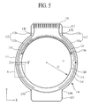
- FIG. 5 is a plane view illustrating a substrate of FIG. 3 .
- the display apparatus may include a substrate 110, a display portion 120, a display pad 130, a flexible printed circuit board 140, a barrier film 150, a polarizing film 160, a cover window 170, a resin coating layer 180 and an insertion member 190.
- the substrate 110 may include a circular arc portion 111 and a driving circuit connecting portion 112. As described above, the substrate 110 may be formed of a flexible plastic material.
- the circular arc portion 111 is formed in a shape of a circular arc by first and second circumference points (CP1, CP2), each of which has the same first radius (r1) based on a center portion of the display portion 120, wherein the first and second circumference points (CP1, CP2) are connected with each other in a straight line.
- the circular arc portion 111 may include a display area (DA), and a non-display area (NDA) surrounding the display area (DA).
- the display area (DA) is formed in a shape of a circle having a second radius (r2) smaller than the first radius (r1), based on the center portion of the circular arc portion 111.
- the circular arc portion 111 and the display area (DA) are substantially formed in a shape of a concentric circle, whereby a bezel width (BW) of the display device, which is defined between an outer sidewall of the substrate 110 and the display area (DA), may be reduced.
- the non-display area includes a peripheral area of the circular arc portion 111 except the display area (DA).
- the driving circuit connecting portion 112 is projected (or extended) from one side of the circular arc portion 111 defined between the first and second circumference points (CP1, CP2).
- the driving circuit connecting portion 112 is prepared in a circular shape on the display area (DA).
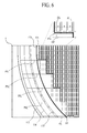
- the display portion 120 may include a plurality of scan lines (SL) disposed at fixed intervals, a plurality of data lines (DL) disposed at fixed intervals and provided in perpendicular to the plurality of scan lines (SL), a plurality of pixel power lines (PL) provided in parallel to the plurality of data lines (DL), and a plurality of pixels (P).
- the plurality of pixels (P) are provided in the display area (DA), wherein the plurality of pixels (P) are arranged in a matrix configuration.
- the pixels (P) adjacent to the non-display area (NDA) may be provided in a shape of a stair along the circumference of the display area (DA). That is, if rectangular pixels (P) are arranged along the circumference of the display area (DA), the circumference (or outermost portion) of the display area (DA) is substantially formed not in a circular shape but in a stair shape.
- the display portion 120 has a resolution higher than a certain level, the circumference of the display area (DA) can be perceived as a shape of a circle, although the pixels at the circumference of the display area (DA) are arranged in a fine stair shape. For this reason, the circular arc portion 111 and the display portion 120 can be regarded as being formed substantially in a shape of a concentric circle.
- the display portion 120 may include dummy pixels (DP) provided in a periphery of the outermost pixels (P) along the circumference of the display area (DA).
- the plurality of dummy pixels (DP) are provided in a boundary between the display area (DA) and the non-display area (NDA).
- the plurality of dummy pixels (DP) reduce or prevent the actual pixels (P) for displaying images from being damaged by external static electricity.
- the number of dummy pixels (DP) at both ends of each pixel row along the circumference of the display area (DA) may vary.
- Each of the plurality of pixels (P) may include a pixel circuit (PC) and an organic light emitting diode (OLED).
- PC pixel circuit
- OLED organic light emitting diode
- the pixel circuit (PC) is connected to the adjacent scan line (SL), data line (DL) and pixel power line (PL), and controls a current flowing in the organic light emitting diode (OLED) in accordance with a data signal (Vdata) from the data line (DL) in response to the scan signal from the scan line (SL) based on a pixel driving power source (Vdd) supplied to the pixel power line (PL).
- the pixel circuit (PC) may include a switching transistor (Tsw), a driving transistor (Tdr), and a capacitor (Cst).
- the switching transistor (Tsw) As the switching transistor (Tsw) is switched in accordance with the scan signal supplied to the scan line (SL), the switching transistor (Tsw) supplies the data signal (Vdata), which is supplied to the data line (DL), to the driving transistor (Tdr). Also, as the driving transistor (Tdr) is switched in accordance with the data signal (Vdata) supplied from the switching transistor (Tsw), the driving transistor (Tdr) controls a data current flowing to the organic light emitting diode (OLED) from the pixel power line (PL).
- OLED organic light emitting diode
- the capacitor (Cst) is connected between a gate terminal and a source terminal of the driving transistor (Tdr), wherein the capacitor (Cst) stores a voltage corresponding to the data signal (Vdata) supplied to the gate terminal of the driving transistor (Tdr), and turns on the driving transistor (Tdr) by the stored voltage.
- the organic light emitting diode may include an anode electrode (or pixel electrode) connected to the source terminal of the driving transistor (Tdr), an organic light emitting layer formed on the anode electrode, and a cathode electrode layer (CE) formed on the organic light emitting layer.
- the organic light emitting diode (OLED) displays a desired image by a light emission in accordance with the data current supplied from the driving transistor (Tdr).
- a driving power supply line 113, a cathode power supply line 114 and a gate-including circuit 115 are formed on the circular arc portion 111 adjacent to the display portion 120.
- the driving power supply line 113 is formed on the substrate 110 along a circumference of the display portion 120, wherein the driving power supply line 113 has predetermined width and thickness, and both ends of the driving power supply line 113 are connected with the display pad 130 in the driving circuit connecting portion 112.
- the driving power supply line 113 serves as a main power line for supplying the pixel driving power source (Vdd) supplied from the display pad 130 to the plurality of pixel power lines (PL) formed in the display portion 120.
- the driving power supply line 113 may be categorized into a circumference line 113a, a first shoulder line 113b, and a second shoulder line 113c in accordance with their positions on the substrate 110.
- the circumference line 113a is formed along a circumference of the remaining display portion 120 except one side of the display portion 120 adjacent to the driving circuit connecting portion 112.
- the circumference line 113a is formed in a shape of a concentric circle with at least one of the display portion 120 and an outer sidewall of the substrate 110.
- the driving power supply line 113 since the driving power supply line 113 is formed at the outmost of the substrate 110, the driving power supply line 113 should be provided at a predetermined distance (D1) from the outer sidewall 110a of the substrate 110 in consideration of inflow of static electricity, etc.
- the circumference line 113a is not formed in a shape of a concentric circle with the display portion 120, the distance (D1) between the outer sidewall 110a of the substrate 110 and the circumference line 113a becomes non-uniform, whereby static electricity may be entered from the circumference line 113a arranged to be relatively close to the outer sidewall 110a of the substrate 110.
- the circumference line 113a is formed in a shape of a concentric circle with the display portion 120, and is also formed in a shape of a concentric circle with the outer sidewall 110a of the substrate 110.
- the first shoulder line 113b is formed between one end of the circumference line 113a adjacent to the driving circuit connecting portion 112 and the display pad 130 with a certain curvature, the first shoulder line 113b connects one end of the circumference line 113a to the display pad 130.
- the first shoulder line 113b is preferably formed with a relatively great curvature to surround the first circumference point (CP1) without being overlapped with the outmost link line formed between the display pad 130 and the display portion 120.
- the second shoulder line 113c is formed between the other end of the circumference line 151 adjacent to the driving circuit connecting portion 112 and the display pad 130 with a certain curvature, the second shoulder line 113c connects the other end of the circumference line 151 to the display pad 130.
- the second shoulder line 113c is preferably formed with a relatively great curvature to surround the second circumference point (CP2) without being overlapped with the outmost link line formed between the display pad 130 and the display portion 120.
- Vdd As the pixel driving power source (Vdd), which is supplied from the display pad 130, is supplied to both ends of the circumference line 113a by the use of first and second shoulder lines 113b and 113c, it is possible to reduce or minimize a voltage drop deviation generated in the driving power supply line 113.
- the driving power supply line 113 is connected with the pixel power line (PL) for each pixel (P) in the display portion 120 through a plurality of power sharing lines (PSL).
- PSL power sharing lines
- Each of the plurality of power sharing lines (PSL) is a unit of a plurality of pixel groups, wherein each pixel group includes at least two of the pixels (P).
- Each of the plurality of power sharing lines (PSL) connects the pixel power line (PL) included in each pixel group to the circumference line 113a of the driving power supply line 113. That is, in order to reduce or prevent a signal interference between the pixel driving power source (Vdd) and the data signal (Vdata), each of the plurality of power sharing lines (PSL) is shared by the two or more pixel power lines (PL) included in each of the pixel groups and being not intersected with the data line (DL).
- each of the plurality of pixel groups may be comprised of two or more rows of the pixels (P) connected to the data line (DL) and the pixel power line (PL), wherein the pixel rows may be set previously based on the curvature of the display portion 120 and may be the same as or different from one another.
- the cathode power supply line 114 is formed between the driving power supply line 113 and the display portion 120 on the substrate 110 along a circumference of the display portion 120, wherein the cathode power supply line 114 has predetermined width and thickness, and both ends of the cathode power supply line 114 are connected to the display pad 130.
- the cathode power supply line 114 according to an example of the present invention may be formed in parallel with the driving power supply line 113 while having the same structure as that of the driving power supply line 113.
- the cathode power supply line 114 is electrically connected with a cathode electrode layer (CE) formed on the circular arc portion 111 to cover the display portion 120, as illustrated in FIG. 8 .
- CE cathode electrode layer
- the cathode power supply line 114 supplies a cathode power, which is supplied from the display pad 130, to the cathode electrode layer (CE), whereby the cathode power is supplied to the organic light emitting diode (OLED) of every pixel (P) formed in the display portion 120 through the cathode electrode layer (CE).
- OLED organic light emitting diode
- the cathode electrode layer (CE) is formed on a passivation layer 116 for covering the pixel circuit (PC) of each pixel (P), and is electrically connected to the organic light emitting layer of the organic light emitting diode (OLED) formed in each pixel (P).
- a corner portion of the cathode electrode layer (CE) is directly connected to the cathode power supply line 114.
- the cathode electrode layer (CE) is formed between the driving power supply line 113 and the display portion 120, whereby a bezel width (BW) of the display apparatus according to the present invention may be reduced.
- the passivation layer 116 can be made of an organic material enabling active water permeation, the passivation layer 116 is beneficially provided at a predetermined distance (D2) from the outer sidewall 110a of the substrate 110 to reduce or prevent the organic light emitting diode (OLED) from being damaged by water permeated into the passivation layer 116.
- the cathode power supply line 114 is beneficially formed between the driving power supply line 113 and the display portion 120 such that the cathode power supply line 114 may be provided at the predetermined distance (D2) from the outer sidewall 110a of the substrate 110, whereby the passivation layer 116 may be provided at the predetermined distance (D2) from the outer sidewall 110a of the substrate 110, and at the same time the bezel width (BW) of the display apparatus, which is defined by a width between the outer sidewall 110a of the substrate 110 and the display portion 120, may be reduced.
- the cathode electrode layer (CE) may be formed to be more adjacent to the outer sidewall 110a of the substrate 110 than the driving power supply line 113.
- the corner portion of the substrate 110 should be extended toward the outskirts to provide the passivation layer 116 at the predetermined distance (D2) from the outer sidewall 110a of the substrate 110, which may increase the bezel width (BW) of the display apparatus.
- the cathode power supply line 114 can be preferably formed between the driving power supply line 113 and the display portion 120.
- the cathode electrode layer (CE) is covered by an encapsulation layer 117.
- the encapsulation layer 117 may be formed in a multi-layered structure in which an organic material layer or an inorganic material layer, the organic material layer and the inorganic material layer are deposited alternately.
- the gate-including circuit 115 is formed in a shape of a circular arc along a circumference of the display portion 120 on the substrate 110, and is connected to each of the plurality of scan lines (SL).
- the gate-including circuit 115 generates the scan signal in response to the scan control signal supplied from the display pad 130, and sequentially supplies the generated scan signal to the plurality of scan lines (SL).
- the gate-including circuit 115 may be formed along a left or right circumference of the display portion 120, to thereby supply the scan signal to one end of the other end of each of the plurality of scan lines (SL).
- the gate-including circuit 115 may be formed along the left and right circumferences of the display portion 120, to thereby supply the scan signal to both ends of each of the plurality of scan lines (SL). Also, the gate-including circuit 115 may be formed along the left and right circumferences of the display portion 120, to thereby supply the scan signal to one end of the odd numbered scan lines (SL) and to supply the scan signal to the other end of the even numbered scan lines (SL).
- the display pad 130 is prepared in the outer circumference of the driving circuit connecting portion 112.
- the display pad 130 may include a plurality of data pads, first and second driving power pads respectively connected to the first and second shoulder lines 113b and 113c, first and second cathode power pads respectively connected with one end and the other end of the cathode power supply line 114, and a plurality of gate pads connected with the gate-including circuit 115.
- the plurality of data pads are connected on one-to-one correspondence to the plurality of data lines (DL) by a plurality of data link lines.
- the first and second driving power pads are connected on one-to-one correspondence to the first and second shoulder lines 113b and 113c.
- the first and second cathode power pads are connected on one-to-one correspondence to one end and the other end of the cathode power supply line 114.
- the plurality of gate pads are connected to the gate-including circuit 115 by a plurality of gate control link lines.
- the flexible printed circuit board 140 is attached to the display pad 130 by a bonding process, wherein the flexible printed circuit board 140 is formed of TCP (Tape Carrier Package) or COF (Chip On Flexible Board or Chip On Film).
- the flexible printed circuit board 140 is bent toward a rear surface of the substrate 110 so as to surround a lateral surface of the substrate 110, and is connected to a driving system.
- the display driving integrated circuit 142 is mounted on the flexible printed circuit board 140.
- the display driving integrated circuit 142 receives a timing synchronization signal and video data supplied from the driving system, converts the video data into the data signal in accordance with the timing synchronization signal, generates a gate control signal in accordance with the timing synchronization signal so as to supply the data signal to the data line (DL) for each pixel (P) through the display pad 130, and supplies the gate control signal to the gate-including circuit 115 through the display pad 130.
- connection portion between the flexible printed circuit board 140 and the display pad 130 may be covered by the resin coating layer 180.
- the resin coating layer 180 is provided to cover the connection portion between the flexible printed circuit board 140 and the display pad 130 by a coating and curing process of a resin material, thereby improving adhesiveness between the flexible printed circuit board 140 and the display pad 130, and simultaneously reducing or preventing moisture or humidity from being permeated into the connection portion between the flexible printed circuit board 140 and the display pad 130.
- the resin coating layer 180 according to an example of the present invention may be formed of thermo-curing resin or photo-curing resin.
- the barrier film 150 is provided on the substrate 110 so as to cover the display portion 120.
- the barrier film 150 may be attached to the encapsulation layer 117 on the upper surface of the display portion 120 by the use of transparent adhesive (not shown).
- the barrier film 150 may be formed of a material with low water permeability, for example, polymer. Meanwhile, a lateral side of the barrier film 150 and a lateral side of the display portion 120 adjacent to the display pad 130 may be sealed by the resin coating layer 180.
- the polarizing film 160 is attached to an upper surface of the barrier film 150, wherein the polarizing film 160 polarizes the light emitted from the display portion 120.
- the cover window 170 is formed of a transparent glass or plasmatic material, wherein the cover window 170 is provided in a circular shape.
- the cover window 170 covers the remaining upper surface of the substrate 100 except the display pad 130 on the substrate 110.
- the cover window 170 is attached to the display portion 120, that is, the upper surface of the polarizing film 160 by the use of transparent adhesive 165 such as OCA (Optical Clear Adhesive), wherein the cover window 170 transmits the light emitted from the display portion 120 to the external environment, and protects the display portion 120.
- OCA Optical Clear Adhesive
- the cover window 170 may be attached to the substrate 110 by a direct bonding process using a roller.
- the direct bonding process may include arranging the cover window 17 on a bonding stage, arranging the substrate 110, which is inverted in a top-and-bottom side, on the cover window 170, attaching the substrate 110 to the cover window 170 by pressing the substrate 110 through the use of pressing roller, and curing the transparent adhesive 165 by ultraviolet rays or heat.
- the transparent adhesive 165 may be coated onto at least one of the substrate 110 and the cover window 170.
- the insertion member 190 is disposed in and inserted into the gap space between an edge of substrate 110, that is, between the driving circuit connecting portion 112 and the cover window 170 confronting each other.
- the insertion member 190 is provided between the resin coating layer 180 and the cover window 170.
- the insertion member 190 may be attached to the upper surface of the resin coating layer 180, and furthermore, may be attached to the rear surface of the cover window 170.
- the insertion member 190 seals the gap space or serves to decrease a step difference between the substrate 110 and the cover window 170 confronting each other with the gap space in-between, to thereby reduce or prevent the substrate 110 from being damaged during the direct bonding process of the cover window 170.
- the display apparatus may further include a selective portion 118 prepared between the display portion 120 and the display pad 130.
- the selective portion 118 is prepared along an upper circumference of the display portion 120 adjacent to the display pad 130.
- the selective portion 118 may include a plurality of selective circuits 118a connected in a unit of two or more data lines.
- Each of the plurality of selective circuits 118a is connected to a plurality of data groups, each of which includes two or more data lines (DL), on one-to-one correspondence, thereby driving the data lines (DL in each data group in a time-division method.
- Each of the plurality of selective circuits 118a may be a multiplexing circuit, for example, multiplexer, which has one input terminal and two or more output terminals.
- the data signal (Vdata) is supplied from the display driving integrated circuit 142 to each input terminal of the plurality of selective circuits 118a.
- the output terminals of the plurality of selective circuits 118a are connected on one-to-one correspondence to the data lines (DL) in each data group.
- Each of the plurality of selective circuits 118a sequentially supplies the data signal (Vdata), which is supplied to the input terminal, to the data lines (DL) in each data group in response to a time-division selective signal.
- the number of data link lines for connecting the display pad 130 and the data line (DL) is decreased so that a formation area of the data link lines is also decreased, to thereby reduce the length between the first and second circumference points (CP1, CP2). Accordingly, it may be possible to provide the display portion 120 and the circular arc portion 111 of the substrate 110 in a more concentric circle, and furthermore to realize the display apparatus with a more-reduced bezel width (BW).
- the barrier film 150 may include a base film, a touch sensing portion prepared on the base film, and a touch circuit connecting portion 151 protruding (or extending) from a lower side of the base film.
- the base film may be formed of a material with low water permeability, for example, polymer.
- the touch sensing portion includes a touch driving line and a touch sensing line overlapped with the display portion 120 and prepared in a touch sensing area defined on the base film.
- the touch circuit connecting portion 151 protrudes (or extends) at a predetermined size from the lower side of the base film, wherein the touch circuit connecting portion 151 is disposed on a support portion 191 of the substrate 110.
- the support portion 119 may be protruding (or extending) from the other side of the circular arc portion 111 defined between third and fourth circumference points (CP3, CP4) having the same first radius (r1) based on the center portion of the display portion 120.
- the touch circuit connecting portion 151 may include a plurality of touch driving link lines connected with the touch driving line of the touch sensing area, a plurality of touch sensing link lines connected with the touch sensing line of the touch sensing area, and a touch pad portion 153 including a plurality of touch pads connected on one-to-one correspondence to the plurality of touch driving link lines and the touch sensing link lines.
- the touch pad portion 153 is connected to a touch flexible printed circuit board 200 by a bonding process, and the touch flexible printed circuit board 200 is bent toward the rear surface of the substrate 110 so as to surround the lateral surface of the substrate 110, and is connected with a touch driving circuit (not shown).
- a connection portion between the touch pad portion 153 and the touch flexible printed circuit board 200 may be sealed by the resin coating layer 180, to thereby improve adhesiveness between the touch pad portion 153 and the touch flexible printed circuit board 200, and to reduce or prevent moisture or humidity from being permeated into the connection portion between the touch pad portion 153 and the touch flexible printed circuit board 200.
- the barrier film 150 may be formed of the base film alone without the touch sensing area, the touch circuit connecting portion 151 and the touch pad portion 153.
- a touch screen (not shown) may be disposed between the barrier film 150 and the polarizing film 160.
- the touch screen may include a touch base film, a touch sensing portion prepared on the touch base film, and a touch circuit connecting portion having a touch pad portion protruding (or extending) from a lower side of the base film and being connected with the touch sensing portion.
- the insertion member 190 is disposed in and inserted into the gap space between the substrate 110 and the cover window 170 being adjacent to the display pad 130 and confronting each other so that it is possible to seal the gap space or to decrease the step difference between the substrate 110 and the cover window 170 in the gap space.
- the display apparatus is provided with the circular arc portion 111 and the display portion 120 formed in the concentric shape so that it is possible to reduce the bezel width (BW) and to thereby reduce a length of the gap space, that is, a length of a long side of the driving circuit connecting portion.
- BW bezel width
- FIGS. 9A to 9C illustrate various examples of an insertion member according to embodiments of the present invention.
- an insertion member 190 may be formed of an elastomer material, and may be provided in a polygonal shape, for example, a rectangular shape.
- the rear surface of the insertion member 190 may be attached to an upper surface of the resin coating layer (180, See FIG. 4 ), and some parts 190u of an upper surface of the insertion member 190 overlapped with the cover window (170, See FIG. 4 ) may be pressed by an edge of the rear surface of the cover window, or may be attached to the edge of the rear surface of the cover window by the use of adhesive.
- a thickness of the insertion member 190 may be greater than a distance between the resin coating layer and the cover window by a preset thickness.
- the insertion member 190 according to the first example of the present invention seals a gap space between the substrate and the cover window confronting each other. Also, the insertion member 190 according to the first example of the present invention is formed of an elastic material so that it is possible to absorb an external force applied to the edge of cover window and/or substrate overlapped with the gap space.
- an insertion member 190 according to the second example of the present invention may have a polygonal shape, for example, a rectangular shape, wherein the insertion member 190 according to the second example of the present invention may include a base member 191, a lower layer 193, and an upper layer 195.
- the base member 191 may be formed of a polymer resin material, or may be formed of the same material as that of the substrate.
- the base member 191 may be formed of an elastomer material.
- the lower layer 193 is attached to a lower surface of the base member 191.
- the lower layer 193 may be formed of an elastomer material or polymer resin material, wherein the material of the lower layer 193 may be different from that of the base member 191.
- the lower layer 193 may be attached to an upper surface of the resin coating layer (180, See FIG. 4 ) by the use of adhesive (not shown).
- the upper layer 195 may be formed of the same material as that of the lower layer 193. Also, some parts 195u of an upper surface of the upper layer 195 overlapped with the cover window (170, See FIG. 4 ) may be pressed by an edge of the rear surface of the cover window, or may be attached to the edge of the rear surface of the cover window by the use of adhesive.
- the insertion member 190 according to the second example of the present invention seals a gap space between the substrate and the cover window confronting each other. Also, the insertion member 190 according to the second example of the present invention is formed in a dual-layered structure including an elastic material so that it is possible to absorb an external force applied to the edge of cover window and/or substrate overlapped with the gap space.
- an insertion member 190 may be formed of an elastomer material, and may be provided in a polygonal shape with a curvature portion 197, for example, a rectangular shape.
- the curvature portion 197 is concavely prepared along a curvature of the cover window from an inner surface of the insertion member 190 confronting the display portion 120.
- An upper edge 197u of the curvature portion 197 may be pressed by an edge of the rear surface of the cover window, or may be attached to the edge of the rear surface of the cover window by the use of adhesive.
- the curvature portion 197 is concavely provided along a curvature of the cover window so that it is possible to seal an entire gap space between the substrate and the cover window on the driving circuit connecting portion.
- the insertion member 190 may be formed in a three-layered structure including a base member 191, a lower layer 193 and an upper layer 195.
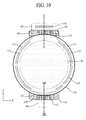
- FIG. 10 is a plane view illustrating a display apparatus according to the second embodiment of the present invention.
- FIG. 11 is a cross-sectional view along I-I' and III-III' of FIG. 10 , wherein an auxiliary insertion member is additionally inserted into a gap space between a cover window and a touch circuit connecting portion prepared on a barrier film. Except the auxiliary insertion member 210, other elements of the display apparatus according to the second embodiment of the present invention are the same as those of the display apparatus according to the first embodiment of the present invention, which are illustrated in FIGS. 3 to 8 . Thus, a detailed description for the same or similar parts will be omitted.
- the auxiliary insertion member 210 is inserted into a gap space between a cover window 170 and a touch circuit connecting portion 151 prepared on a lower surface of a barrier film 150. At this time, the gap space between the touch circuit connecting portion 151 and the cover window 170 may occur on the touch circuit connecting portion 151 for a connection between a touch flexible printed circuit board 200 and a touch pad portion 153.
- auxiliary insertion member 210 is provided in the gap space between the touch circuit connecting portion 151 and the cover window 180, it is possible to seal the gap space or to reduce a step difference between the cover window 170 and the touch circuit connecting portion 1 151 of the barrier film 150 confronting each other with the gap space in-between, thereby reducing or preventing the substrate 110 from being damaged during a bonding process of the cover window 170.
- the auxiliary insertion member 210 may be similar or the same in structure as the insertion member 190 illustrated in any one of FIGS. 9A to 9C .
- the auxiliary insertion member 210 may be prepared between the cover window 170 and the touch circuit connecting portion 151 in accordance with similar or the same manufacturing method as that of the insertion member 190.
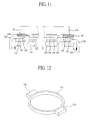
- connection ring member 220 the insertion member 190 is protruding from one side of the connection ring member 220, and the auxiliary insertion member 210 is protruding from the other side of the connection ring member 220.
- the connection ring member 220, the insertion member 190 and the auxiliary insertion member 210 may be formed as one body.
- connection ring member 220 is formed in a ring shape while being overlapped with an edge of the cover window (170 in FIG. 11 ).
- the connection ring member 220 is disposed in and inserted into a gap space between an edge of cover window and an edge of circular arc portion (111 in FIG. 11 ) of the substrate 110, to thereby reduce or prevent foreign matters from being permeated into the gap space between the edge of the cover window and the edge of the circular arc portion 111 of the substrate 110.
- the display apparatus it is possible to reduce or prevent the substrate 110 from being damaged by the gap space between the substrate110 and the cover window 170 respectively adjacent to the display pad 130 and the touch pad portion 153 during a direct bonding process between the substrate 110 and the cover window 170, or to reduce or prevent the substrate 110 or the cover window 170 overlapped with the gap space from being damaged by an external force.
- the insertion member 190 is provided in the gap space between the edge of the substrate 110 and the edge of the cover window 170 so that it is possible to reduce or prevent the substrate 110 from being damaged by the external force applied to the edge of the cover window 170 and/or the substrate 110 overlapped with the gap space, thereby improving reliability of the substrate 110.
- the bezel width (BW) can be reduced by the circular arc portion 111 and the display portion 120 formed in a shape of concentric circle.
- the driving power supply line 113 is prepared in the periphery of the circular arc portion 111, and the cathode power supply line 114 is prepared between the driving power supply line 113 and the display portion 120 so that it is possible to realize a more-reduced bezel width (BW).
Landscapes
- Physics & Mathematics (AREA)
- Nonlinear Science (AREA)
- General Physics & Mathematics (AREA)
- Optics & Photonics (AREA)
- Mathematical Physics (AREA)
- Chemical & Material Sciences (AREA)
- Crystallography & Structural Chemistry (AREA)
- Engineering & Computer Science (AREA)
- Microelectronics & Electronic Packaging (AREA)
- Electroluminescent Light Sources (AREA)
- Devices For Indicating Variable Information By Combining Individual Elements (AREA)
- Electric Clocks (AREA)
Abstract
Description
- This application claims the benefit of the Korean Patent Application No.
10-2014-0141901 filed on October 20, 2014 - The present invention relates to a display apparatus and a method of manufacturing the same, and more particularly, to a display apparatus having a circular display portion.
- Generally, display apparatuses have been widely used as the screens of various products such as televisions, notebook computers and monitors as well as portable electronic devices such as mobile communication terminals, electronic diaries, electronic books, portable multimedia players (PMPs), navigation systems, ultra mobile PCs (UMPCs), mobile phones, smart phones, tablet PCs (personal computers) and watch phones.
- Studies for developing flexible display apparatuses have been made, focusing on liquid crystal display apparatuses, organic light emitting display apparatuses and electrophoretic display apparatuses due to their slim sizes.
- An organic light emitting display apparatus displays a desired picture image by controlling an amount of current that flows from a pixel power line to the organic light emitting diode in accordance with a data signal. Such an organic light emitting display apparatus typically has a rectangular display screen due to arrangement structures of signal lines, pixel driving power lines and driving circuits.
- Recently, as appearance and design of display apparatuses have become more important and consumers' attention to wearable devices such as watch phones has increased, studies and developments of a display apparatus having a circular display screen, not a rectangular display screen, have been made.
-
FIG. 1 is a cross-sectional view illustrating some parts of a display apparatus having a circular display portion according to the related art. - Referring to
FIG. 1 , the display apparatus having a circular display portion according to the related art is formed of a plastic material. The display apparatus includes asubstrate 10 having a circular display area (DA) and a non-display area (NDA) in a periphery of the display area (DA), thedisplay portion 20 in the display area (DA) of thesubstrate 10, apad 30 at one side of the non-display area (NDA) of thesubstrate 10, a flexible printedcircuit board 40 attached to thepad 30 and provided to supply signals to thedisplay portion 20 through thepad 30, abarrier film 50 on thedisplay portion 20 that is provided to cover an upper surface of thesubstrate 10 except thepad 30, a polarizingfilm 60 attached to an upper surface of thebarrier film 50, acover window 70 attached to an upper surface of the polarizingfilm 60 by the use oftransparent adhesive 65 and provided to cover the upper surface of thesubstrate 10, and aresin coating layer 80 coated and cured at a connection portion between the flexible printedcircuit board 40 and thepad 30 of thesubstrate 10. - The
display portion 20 may include an organic light emitting diode (not shown) and a pixel circuit (not shown) that controls the organic light emitting diode to emit light in accordance with a signal supplied from the flexible printedcircuit board 40 via thepad 30. - A gap space (GS) may exist between the
substrate 10 and thecover window 70 at a driving circuit connecting portion of the display apparatus according to the related art. The gap space (GS) at the driving circuit connecting portion may facilitate connecting the flexible printedcircuit board 40 with thepad 30 of thesubstrate 10, attaching the polarizingfilm 60 and coating thetransparent adhesive 65 during the manufacturing processes. - The gap space (GS) may cause micro-cracks to occur on the
substrate 10 due to an external force, such as bonding force or adhering force applied to thesubstrate 10, during a direct bonding process for attaching thecover window 70 to the upper surface of the polarizingfilm 60, thereby lowering reliability of thesubstrate 10. - The gap space (GS) may be sealed by the
resin coating layer 80 used to improve adhesiveness between the flexible printedcircuit board 40 and thepad 30 of thesubstrate 10. However, it may be difficult to fill theresin coating layer 80 in the gap space (GS). Also, if a thickness of theresin coating layer 80 increases, a processing time for curing theresin coating layer 80 increases, thereby decreasing productivity. Moreover, theresin coating layer 80 filled in the gap space (GS) may spread during the attachment process of thecover window 70, which may contaminate a peripheral area of the display apparatus. In order to prevent such a contamination at the peripheral area, an additional process such as forming a separate dam structure may be needed. - The above description for the display apparatus having the circular display portion using the organic light emitting diode is technical information which was possessed by the inventor when deriving some or part of the present invention. Thus, the above description may not be prior art.
- Accordingly, the present invention is directed to a display apparatus and method for manufacturing the same that substantially obviates one or more of the problems due to limitations and disadvantages of the related art.
- An advantage of the present invention is to provide to provide a display apparatus having a circular display portion with improved reliability.
- Additional features and advantages of the invention will be set forth in the description which follows, and in part will be apparent from the description, or may be learned by practice of the invention. These and other advantages of the invention will be realized and attained by the structure particularly pointed out in the written description and claims hereof as well as the appended drawings.
- To achieve these and other advantages and in accordance with the purpose of the present invention, as embodied and broadly described, a display apparatus may, for example, include a display portion including a plurality of pixels; a driving circuit connecting portion outside the display portion on a substrate; a plurality of display pads in the driving circuit connecting portion that are electrically connected to the plurality of pixels, respectively; a cover window on the substrate that covers the display portion and exposes a part of the substrate; and an insertion member in the driving circuit connecting portion in a gap space between the substrate and the cover window, wherein the insertion member is extended over to the exposed part of the substrate.
- At this time, the cover window may be formed in a circular shape for covering the display portion, and the insertion member may be formed in a polygonal shape overlapped with the edge of the cover window.
- The substrate may further include a cathode power supply line and a driving power supply line connected with a pixel prepared in the display portion, wherein the cathode power supply line may be prepared between the display portion and the driving power supply line prepared in an edge of a circular arc portion of the substrate.
- In another aspect of the present invention, a display apparatus may, for example, include a display portion having a circular shape on a circular arc portion of a substrate, the substrate including the circular arc portion and a driving circuit connecting portion protruding from one side of the circular arc portion; a cover window on the substrate that covers the display portion; and an insertion member in a gap space between an edge of the substrate and an edge of the cover window, and interposed between the driving circuit connecting portion and the cover window.
- It is to be understood that both the foregoing general description and the following detailed description are exemplary and explanatory and are intended to provide further explanation of the invention as claimed.
- The accompanying drawings, which are included to provide a further understanding of the invention and are incorporated in and constitute a part of this specification, illustrate embodiments of the invention and together with the description serve to explain the principles of the invention. In the drawings:
-
FIG. 1 is a cross-sectional view illustrating some parts of a display apparatus having a circular display portion according to the related art; -
FIG. 2 is a cross-sectional view illustrating a side of a display apparatus according to the embodiment of the present invention; -
FIG. 3 is a plane view illustrating a display apparatus according to the first embodiment of the present invention; -
FIG. 4 is a cross-sectional view along I-I' ofFIG. 3 ; -
FIG. 5 is a plane view illustrating a substrate ofFIG. 3 ; -
FIG. 6 is an expanded view illustrating 'A' ofFIG. 5 ; -
FIG. 7 is a circuit diagram illustrating a pixel ofFIG. 6 ; -
FIG. 8 is a cross-sectional view along II-II' ofFIG. 5 ; -
FIGS. 9A to 9C illustrate various examples of an insertion member in a display apparatus according to embodiments of the present invention; -
FIG. 10 is a plane view illustrating a display apparatus according to the second embodiment of the present invention; -
FIG. 11 is a cross-sectional view along I-I' and III-III' ofFIG. 10 ; and -
FIG. 12 illustrates a connection ring member for connecting an insertion member and an auxiliary insertion member illustrated inFIG. 10 . - Reference will now be made in detail to exemplary embodiments of the present invention, examples of which are illustrated in the accompanying drawings. Wherever possible, the same reference numbers will be used throughout the drawings to refer to the same or like parts. In the following description, detailed description of known elements or functions may be omitted.
- Terms disclosed in this specification should be understood as follows.
- The term of a singular expression should be understood to include a multiple expression as well as the singular expression if there is no specific definition in the context. The terms such as "the first" and "the second" are used only to differentiate one element from other elements. Thus, a scope of claims is not limited by these terms. Also, it should be understood that the term such as "include" or "have" does not preclude existence or possibility of one or more features, numbers, steps, operations, elements, parts or their combinations. It should be understood that the term "at least one" includes all combinations related with any one item. For example, "at least one among a first element, a second element and a third element" may include all combinations of two or more elements selected from the first, second and third elements as well as each element of the first, second and third elements. Also, if it is mentioned that a first element is positioned "on or above" a second element, it should be understood that the first and second elements may be brought into contact with each other, or a third element may be interposed between the first and second elements.
-
FIG. 2 is a cross-sectional view illustrating a side of a display apparatus according to one embodiment of the present invention. - Referring to
FIG. 2 , the display apparatus may include asubstrate 110, adisplay portion 120, acover window 170, and aninsertion member 190. - The
substrate 110 may include a display area (DA) in a circular shape, and a non-display area (NDA) in a periphery of the display area (DA). Thesubstrate 110 may be formed of a flexible plastic material, for example, an opaque or colored polyimide (PI) material. - A support substrate (not shown) may be additionally attached to a rear surface of the
substrate 110. The support substrate maintains a shape of thesubstrate 110. The support substrate may be formed of a polymer resin material whose flexibility is lower than that of thesubstrate 110, for example, any one of PET (polyethyleneterephthalate), PC (polycarbonate), PES (polyethersulfone), PEN (polyethylenapthanate) and PNB (polynorborneen). Thesubstrate 110 may also be formed of a non-flexible material. In this case, the support substrate may be beneficially omitted so as to realize slimness of the display apparatus. - The
display portion 120 is formed in a circular shape in the display area (DA) on thesubstrate 110. Thedisplay portion 120 may be an organic light emitting device and include a plurality of pixels. The plurality of pixels display a predetermined image through a light emission of the organic light emitting device in accordance with a driving signal supplied via adisplay pad 130 at one side of thesubstrate 110. Thedisplay portion 120 may include an encapsulation layer for covering the plurality of pixels. - The
display pad 130 is connected with a flexible printedcircuit board 140, wherein thedisplay pad 130 transmits driving signals, which are supplied through the flexible printedcircuit board 140, to each pixel. - One side of the flexible printed
circuit board 140 is attached to thedisplay pad 130, and the other side of the flexible printedcircuit board 140 is connected with a driving system of the display apparatus. A display drivingintegrated circuit 142 is mounted on the flexible printedcircuit board 140. The display drivingintegrated circuit 142 generates driving signals including a data signal and a control signal for controlling the light emission of the organic light emitting device from digital data and control signals supplied from the driving system, and supplies the driving signals to each pixel. - A connection portion between the flexible printed
circuit board 140 and thedisplay pad 130 is sealed by aresin coating layer 180. Theresin coating layer 180 may improve adhesiveness between the flexible printedcircuit board 140 and thedisplay pad 130, and simultaneously reduce or prevent moisture or humidity from being permeated into the connection portion between the flexible printedcircuit board 140 and thedisplay pad 130. Theresin coating layer 180 may be formed of thermo-curing resin or photo-curing resin that is coated and cured on the connection portion between the flexible printedcircuit board 140 and thedisplay pad 130. - Meanwhile, the
substrate 110 may include a gate-including circuit (not shown) in the non-display area (NDA) along a curvature of the display area (DA). The gate-including circuit generates a scan signal in response to a scan control signal supplied from the display drivingintegrated circuit 142, and supplies the generated scan signal to each pixel. - The
cover window 170 is formed of a transparent glass or plasmatic material, wherein thecover window 170 is provided in a circular shape. Thecover window 170 covers thedisplay portion 120 except thedisplay pad 130 on thesubstrate 110. Thecover window 170, which is attached to thedisplay portion 120 by the use oftransparent adhesive 165, transmits the light emitted from thedisplay portion 120 to the external environment. - As illustrated in
FIG. 2 , theinsertion member 190 is disposed in and inserted into a gap space between an edge of thecover window 170 and an edge ofsubstrate 110 confronting each other. - The gap space is provided on the
display pad 130 to facilitate connecting the flexible printedcircuit board 140 and thedisplay pad 130. During a direct bonding process for attaching thecover window 170 to thedisplay portion 120, micro-cracks may occur in thesubstrate 110 by an external force such as bonding force or adhering force applied to thesubstrate 110 overlapped with the gap space. - The
insertion member 190 inserted into the gap space may seal the gap space or decrease a step difference between thesubstrate 110 and thecover window 170, to thereby reduce or prevent thesubstrate 110 from being damaged during the direct bonding process of thecover window 170 by an external force applied to an edge of thecover window 170 and/or thesubstrate 110 overlapped with the gap space. - The
insertion member 190 according to an example of the present invention may include an elastomer material. Theinsertion member 190 is attached to an upper surface of theresin coating layer 180 by the use of adhesive (not shown) provided on its lower surface. Furthermore, theinsertion member 190 may be additionally attached to a rear surface of thecover window 170 by the use of adhesive provided on its upper surface. - As illustrated in the expanded view of
FIG. 2 , theinsertion member 190 according to another example of the present invention may include abase member 191, alower layer 193 on a lower surface of thebase member 191, and anupper layer 195 on an upper surface of thebase member 191. In this case, thebase member 191 may be formed of a polymer resin or elastomer material. Each of thelower layer 193 and theupper layer 195 may be selectively formed of a polymer resin or elastomer material, wherein the material for each of thelower layer 193 and theupper layer 195 may be different from that of thebase member 191. Theinsertion member 190 may be attached to an upper surface of theresin coating layer 180 by the use of adhesive (not shown) on a lower surface of thelower layer 193. Furthermore, theinsertion member 190 may be additionally attached to a rear surface of thecover window 170 by the use of adhesive on theupper layer 195. - As described above, the
insertion member 190 is disposed in and inserted into the gap space between the edge of thesubstrate 110 and the edge of thecover window 170, and it is thus possible to reduce or prevent thesubstrate 110 from being damaged during the subsequent bonding process of thecover window 170, thereby improving reliability in thesubstrate 110. -
FIG. 3 is a plane view illustrating a display apparatus according to the first embodiment of the present invention.FIG. 4 is a cross-sectional view along I-I' ofFIG. 3 .FIG. 5 is a plane view illustrating a substrate ofFIG. 3 . - Referring to
FIGS. 3 to 5 , the display apparatus according to the first embodiment of the present invention may include asubstrate 110, adisplay portion 120, adisplay pad 130, a flexible printedcircuit board 140, abarrier film 150, apolarizing film 160, acover window 170, aresin coating layer 180 and aninsertion member 190. - The
substrate 110 may include acircular arc portion 111 and a drivingcircuit connecting portion 112. As described above, thesubstrate 110 may be formed of a flexible plastic material. - The
circular arc portion 111 is formed in a shape of a circular arc by first and second circumference points (CP1, CP2), each of which has the same first radius (r1) based on a center portion of thedisplay portion 120, wherein the first and second circumference points (CP1, CP2) are connected with each other in a straight line. Thecircular arc portion 111 may include a display area (DA), and a non-display area (NDA) surrounding the display area (DA). - The display area (DA) is formed in a shape of a circle having a second radius (r2) smaller than the first radius (r1), based on the center portion of the
circular arc portion 111. At this time, thecircular arc portion 111 and the display area (DA) are substantially formed in a shape of a concentric circle, whereby a bezel width (BW) of the display device, which is defined between an outer sidewall of thesubstrate 110 and the display area (DA), may be reduced. - The non-display area (NDA) includes a peripheral area of the
circular arc portion 111 except the display area (DA). - The driving
circuit connecting portion 112 is projected (or extended) from one side of thecircular arc portion 111 defined between the first and second circumference points (CP1, CP2). - The driving
circuit connecting portion 112 is prepared in a circular shape on the display area (DA). As illustrated inFIGS. 6 and7 , thedisplay portion 120 may include a plurality of scan lines (SL) disposed at fixed intervals, a plurality of data lines (DL) disposed at fixed intervals and provided in perpendicular to the plurality of scan lines (SL), a plurality of pixel power lines (PL) provided in parallel to the plurality of data lines (DL), and a plurality of pixels (P). - The plurality of pixels (P) are provided in the display area (DA), wherein the plurality of pixels (P) are arranged in a matrix configuration. In this case, the pixels (P) adjacent to the non-display area (NDA) may be provided in a shape of a stair along the circumference of the display area (DA). That is, if rectangular pixels (P) are arranged along the circumference of the display area (DA), the circumference (or outermost portion) of the display area (DA) is substantially formed not in a circular shape but in a stair shape. However, if the
display portion 120 has a resolution higher than a certain level, the circumference of the display area (DA) can be perceived as a shape of a circle, although the pixels at the circumference of the display area (DA) are arranged in a fine stair shape. For this reason, thecircular arc portion 111 and thedisplay portion 120 can be regarded as being formed substantially in a shape of a concentric circle. - Additionally, the
display portion 120 may include dummy pixels (DP) provided in a periphery of the outermost pixels (P) along the circumference of the display area (DA). In this case, the plurality of dummy pixels (DP) are provided in a boundary between the display area (DA) and the non-display area (NDA). The plurality of dummy pixels (DP) reduce or prevent the actual pixels (P) for displaying images from being damaged by external static electricity. At this time, the number of dummy pixels (DP) at both ends of each pixel row along the circumference of the display area (DA) may vary. - Each of the plurality of pixels (P) may include a pixel circuit (PC) and an organic light emitting diode (OLED).
- The pixel circuit (PC) is connected to the adjacent scan line (SL), data line (DL) and pixel power line (PL), and controls a current flowing in the organic light emitting diode (OLED) in accordance with a data signal (Vdata) from the data line (DL) in response to the scan signal from the scan line (SL) based on a pixel driving power source (Vdd) supplied to the pixel power line (PL). The pixel circuit (PC) according to an example of the present invention may include a switching transistor (Tsw), a driving transistor (Tdr), and a capacitor (Cst).
- As the switching transistor (Tsw) is switched in accordance with the scan signal supplied to the scan line (SL), the switching transistor (Tsw) supplies the data signal (Vdata), which is supplied to the data line (DL), to the driving transistor (Tdr). Also, as the driving transistor (Tdr) is switched in accordance with the data signal (Vdata) supplied from the switching transistor (Tsw), the driving transistor (Tdr) controls a data current flowing to the organic light emitting diode (OLED) from the pixel power line (PL). The capacitor (Cst) is connected between a gate terminal and a source terminal of the driving transistor (Tdr), wherein the capacitor (Cst) stores a voltage corresponding to the data signal (Vdata) supplied to the gate terminal of the driving transistor (Tdr), and turns on the driving transistor (Tdr) by the stored voltage.
- The organic light emitting diode (OLED) may include an anode electrode (or pixel electrode) connected to the source terminal of the driving transistor (Tdr), an organic light emitting layer formed on the anode electrode, and a cathode electrode layer (CE) formed on the organic light emitting layer. The organic light emitting diode (OLED) displays a desired image by a light emission in accordance with the data current supplied from the driving transistor (Tdr).
- Referring back to
FIGS. 3 to 7 , a drivingpower supply line 113, a cathodepower supply line 114 and a gate-includingcircuit 115 are formed on thecircular arc portion 111 adjacent to thedisplay portion 120. - The driving
power supply line 113 is formed on thesubstrate 110 along a circumference of thedisplay portion 120, wherein the drivingpower supply line 113 has predetermined width and thickness, and both ends of the drivingpower supply line 113 are connected with thedisplay pad 130 in the drivingcircuit connecting portion 112. The drivingpower supply line 113 serves as a main power line for supplying the pixel driving power source (Vdd) supplied from thedisplay pad 130 to the plurality of pixel power lines (PL) formed in thedisplay portion 120. - The driving
power supply line 113 according to an example of the present invention may be categorized into acircumference line 113a, afirst shoulder line 113b, and asecond shoulder line 113c in accordance with their positions on thesubstrate 110. - The
circumference line 113a is formed along a circumference of the remainingdisplay portion 120 except one side of thedisplay portion 120 adjacent to the drivingcircuit connecting portion 112. Preferably, thecircumference line 113a is formed in a shape of a concentric circle with at least one of thedisplay portion 120 and an outer sidewall of thesubstrate 110. At this time, as illustrated inFIG. 8 , since the drivingpower supply line 113 is formed at the outmost of thesubstrate 110, the drivingpower supply line 113 should be provided at a predetermined distance (D1) from theouter sidewall 110a of thesubstrate 110 in consideration of inflow of static electricity, etc. If thecircumference line 113a is not formed in a shape of a concentric circle with thedisplay portion 120, the distance (D1) between theouter sidewall 110a of thesubstrate 110 and thecircumference line 113a becomes non-uniform, whereby static electricity may be entered from thecircumference line 113a arranged to be relatively close to theouter sidewall 110a of thesubstrate 110. Preferably, thecircumference line 113a is formed in a shape of a concentric circle with thedisplay portion 120, and is also formed in a shape of a concentric circle with theouter sidewall 110a of thesubstrate 110. - As the
first shoulder line 113b is formed between one end of thecircumference line 113a adjacent to the drivingcircuit connecting portion 112 and thedisplay pad 130 with a certain curvature, thefirst shoulder line 113b connects one end of thecircumference line 113a to thedisplay pad 130. Thefirst shoulder line 113b is preferably formed with a relatively great curvature to surround the first circumference point (CP1) without being overlapped with the outmost link line formed between thedisplay pad 130 and thedisplay portion 120. - As the
second shoulder line 113c is formed between the other end of thecircumference line 151 adjacent to the drivingcircuit connecting portion 112 and thedisplay pad 130 with a certain curvature, thesecond shoulder line 113c connects the other end of thecircumference line 151 to thedisplay pad 130. Thesecond shoulder line 113c is preferably formed with a relatively great curvature to surround the second circumference point (CP2) without being overlapped with the outmost link line formed between thedisplay pad 130 and thedisplay portion 120. - As the pixel driving power source (Vdd), which is supplied from the
display pad 130, is supplied to both ends of thecircumference line 113a by the use of first andsecond shoulder lines power supply line 113. - The driving
power supply line 113 is connected with the pixel power line (PL) for each pixel (P) in thedisplay portion 120 through a plurality of power sharing lines (PSL). - Each of the plurality of power sharing lines (PSL) is a unit of a plurality of pixel groups, wherein each pixel group includes at least two of the pixels (P). Each of the plurality of power sharing lines (PSL) connects the pixel power line (PL) included in each pixel group to the
circumference line 113a of the drivingpower supply line 113. That is, in order to reduce or prevent a signal interference between the pixel driving power source (Vdd) and the data signal (Vdata), each of the plurality of power sharing lines (PSL) is shared by the two or more pixel power lines (PL) included in each of the pixel groups and being not intersected with the data line (DL). In this case, each of the plurality of pixel groups may be comprised of two or more rows of the pixels (P) connected to the data line (DL) and the pixel power line (PL), wherein the pixel rows may be set previously based on the curvature of thedisplay portion 120 and may be the same as or different from one another. - The cathode
power supply line 114 is formed between the drivingpower supply line 113 and thedisplay portion 120 on thesubstrate 110 along a circumference of thedisplay portion 120, wherein the cathodepower supply line 114 has predetermined width and thickness, and both ends of the cathodepower supply line 114 are connected to thedisplay pad 130. The cathodepower supply line 114 according to an example of the present invention may be formed in parallel with the drivingpower supply line 113 while having the same structure as that of the drivingpower supply line 113. The cathodepower supply line 114 is electrically connected with a cathode electrode layer (CE) formed on thecircular arc portion 111 to cover thedisplay portion 120, as illustrated inFIG. 8 . The cathodepower supply line 114 supplies a cathode power, which is supplied from thedisplay pad 130, to the cathode electrode layer (CE), whereby the cathode power is supplied to the organic light emitting diode (OLED) of every pixel (P) formed in thedisplay portion 120 through the cathode electrode layer (CE). - The cathode electrode layer (CE) is formed on a
passivation layer 116 for covering the pixel circuit (PC) of each pixel (P), and is electrically connected to the organic light emitting layer of the organic light emitting diode (OLED) formed in each pixel (P). A corner portion of the cathode electrode layer (CE) is directly connected to the cathodepower supply line 114. - The cathode electrode layer (CE) is formed between the driving
power supply line 113 and thedisplay portion 120, whereby a bezel width (BW) of the display apparatus according to the present invention may be reduced. In more detail, since thepassivation layer 116 can be made of an organic material enabling active water permeation, thepassivation layer 116 is beneficially provided at a predetermined distance (D2) from theouter sidewall 110a of thesubstrate 110 to reduce or prevent the organic light emitting diode (OLED) from being damaged by water permeated into thepassivation layer 116. As a result, the cathodepower supply line 114 according to an example of the present invention is beneficially formed between the drivingpower supply line 113 and thedisplay portion 120 such that the cathodepower supply line 114 may be provided at the predetermined distance (D2) from theouter sidewall 110a of thesubstrate 110, whereby thepassivation layer 116 may be provided at the predetermined distance (D2) from theouter sidewall 110a of thesubstrate 110, and at the same time the bezel width (BW) of the display apparatus, which is defined by a width between theouter sidewall 110a of thesubstrate 110 and thedisplay portion 120, may be reduced. - Meanwhile, the cathode electrode layer (CE) may be formed to be more adjacent to the
outer sidewall 110a of thesubstrate 110 than the drivingpower supply line 113. In this case, the corner portion of thesubstrate 110 should be extended toward the outskirts to provide thepassivation layer 116 at the predetermined distance (D2) from theouter sidewall 110a of thesubstrate 110, which may increase the bezel width (BW) of the display apparatus. In order to reduce the bezel width (BW) of the display apparatus and to provide thepassivation layer 116 at the predetermined distance (D2) from theouter sidewall 110a of thesubstrate 110, the cathodepower supply line 114 can be preferably formed between the drivingpower supply line 113 and thedisplay portion 120. - The cathode electrode layer (CE) is covered by an
encapsulation layer 117. Theencapsulation layer 117 may be formed in a multi-layered structure in which an organic material layer or an inorganic material layer, the organic material layer and the inorganic material layer are deposited alternately. - To form a thin film transistor in each pixel (P), the gate-including
circuit 115 is formed in a shape of a circular arc along a circumference of thedisplay portion 120 on thesubstrate 110, and is connected to each of the plurality of scan lines (SL). The gate-includingcircuit 115 generates the scan signal in response to the scan control signal supplied from thedisplay pad 130, and sequentially supplies the generated scan signal to the plurality of scan lines (SL). The gate-includingcircuit 115 may be formed along a left or right circumference of thedisplay portion 120, to thereby supply the scan signal to one end of the other end of each of the plurality of scan lines (SL). Alternatively, the gate-includingcircuit 115 may be formed along the left and right circumferences of thedisplay portion 120, to thereby supply the scan signal to both ends of each of the plurality of scan lines (SL). Also, the gate-includingcircuit 115 may be formed along the left and right circumferences of thedisplay portion 120, to thereby supply the scan signal to one end of the odd numbered scan lines (SL) and to supply the scan signal to the other end of the even numbered scan lines (SL). - Referring back to
FIGS. 3 to 5 , thedisplay pad 130 is prepared in the outer circumference of the drivingcircuit connecting portion 112. Thedisplay pad 130 may include a plurality of data pads, first and second driving power pads respectively connected to the first andsecond shoulder lines power supply line 114, and a plurality of gate pads connected with the gate-includingcircuit 115. - The plurality of data pads are connected on one-to-one correspondence to the plurality of data lines (DL) by a plurality of data link lines. The first and second driving power pads are connected on one-to-one correspondence to the first and
second shoulder lines power supply line 114. The plurality of gate pads are connected to the gate-includingcircuit 115 by a plurality of gate control link lines. - The flexible printed
circuit board 140 is attached to thedisplay pad 130 by a bonding process, wherein the flexible printedcircuit board 140 is formed of TCP (Tape Carrier Package) or COF (Chip On Flexible Board or Chip On Film). The flexible printedcircuit board 140 is bent toward a rear surface of thesubstrate 110 so as to surround a lateral surface of thesubstrate 110, and is connected to a driving system. - The display driving
integrated circuit 142 is mounted on the flexible printedcircuit board 140. - The display driving
integrated circuit 142 receives a timing synchronization signal and video data supplied from the driving system, converts the video data into the data signal in accordance with the timing synchronization signal, generates a gate control signal in accordance with the timing synchronization signal so as to supply the data signal to the data line (DL) for each pixel (P) through thedisplay pad 130, and supplies the gate control signal to the gate-includingcircuit 115 through thedisplay pad 130. - The connection portion between the flexible printed
circuit board 140 and thedisplay pad 130 may be covered by theresin coating layer 180. - The
resin coating layer 180 is provided to cover the connection portion between the flexible printedcircuit board 140 and thedisplay pad 130 by a coating and curing process of a resin material, thereby improving adhesiveness between the flexible printedcircuit board 140 and thedisplay pad 130, and simultaneously reducing or preventing moisture or humidity from being permeated into the connection portion between the flexible printedcircuit board 140 and thedisplay pad 130. Theresin coating layer 180 according to an example of the present invention may be formed of thermo-curing resin or photo-curing resin. - Referring back to
FIGS. 3 and4 , thebarrier film 150 is provided on thesubstrate 110 so as to cover thedisplay portion 120. In this case, thebarrier film 150 may be attached to theencapsulation layer 117 on the upper surface of thedisplay portion 120 by the use of transparent adhesive (not shown). Thebarrier film 150 may be formed of a material with low water permeability, for example, polymer. Meanwhile, a lateral side of thebarrier film 150 and a lateral side of thedisplay portion 120 adjacent to thedisplay pad 130 may be sealed by theresin coating layer 180. - The
polarizing film 160 is attached to an upper surface of thebarrier film 150, wherein thepolarizing film 160 polarizes the light emitted from thedisplay portion 120. - The
cover window 170 is formed of a transparent glass or plasmatic material, wherein thecover window 170 is provided in a circular shape. Thecover window 170 covers the remaining upper surface of the substrate 100 except thedisplay pad 130 on thesubstrate 110. Thecover window 170 is attached to thedisplay portion 120, that is, the upper surface of thepolarizing film 160 by the use of transparent adhesive 165 such as OCA (Optical Clear Adhesive), wherein thecover window 170 transmits the light emitted from thedisplay portion 120 to the external environment, and protects thedisplay portion 120. For connection between the flexible printedcircuit board 140 and thedisplay pad 130, the gap space is prepared between thecover window 170 and the drivingcircuit connecting portion 112 of thesubstrate 110. - Additionally, the
cover window 170 may be attached to thesubstrate 110 by a direct bonding process using a roller. The direct bonding process according to an example of the present invention may include arranging the cover window 17 on a bonding stage, arranging thesubstrate 110, which is inverted in a top-and-bottom side, on thecover window 170, attaching thesubstrate 110 to thecover window 170 by pressing thesubstrate 110 through the use of pressing roller, and curing thetransparent adhesive 165 by ultraviolet rays or heat. At this time, thetransparent adhesive 165 may be coated onto at least one of thesubstrate 110 and thecover window 170. - The
insertion member 190 is disposed in and inserted into the gap space between an edge ofsubstrate 110, that is, between the drivingcircuit connecting portion 112 and thecover window 170 confronting each other. In other words, theinsertion member 190 is provided between theresin coating layer 180 and thecover window 170. Theinsertion member 190 may be attached to the upper surface of theresin coating layer 180, and furthermore, may be attached to the rear surface of thecover window 170. Theinsertion member 190 seals the gap space or serves to decrease a step difference between thesubstrate 110 and thecover window 170 confronting each other with the gap space in-between, to thereby reduce or prevent thesubstrate 110 from being damaged during the direct bonding process of thecover window 170. - Referring back to
FIGS. 3 to 5 , the display apparatus according to the first embodiment of the present invention may further include aselective portion 118 prepared between thedisplay portion 120 and thedisplay pad 130. - The
selective portion 118 is prepared along an upper circumference of thedisplay portion 120 adjacent to thedisplay pad 130. Theselective portion 118 may include a plurality ofselective circuits 118a connected in a unit of two or more data lines. Each of the plurality ofselective circuits 118a is connected to a plurality of data groups, each of which includes two or more data lines (DL), on one-to-one correspondence, thereby driving the data lines (DL in each data group in a time-division method. Each of the plurality ofselective circuits 118a according to an example of the present invention may be a multiplexing circuit, for example, multiplexer, which has one input terminal and two or more output terminals. The data signal (Vdata) is supplied from the display drivingintegrated circuit 142 to each input terminal of the plurality ofselective circuits 118a. The output terminals of the plurality ofselective circuits 118a are connected on one-to-one correspondence to the data lines (DL) in each data group. Each of the plurality ofselective circuits 118a sequentially supplies the data signal (Vdata), which is supplied to the input terminal, to the data lines (DL) in each data group in response to a time-division selective signal. - In the display apparatus including the
selective portion 118 according to the first embodiment of the present invention, the number of data link lines for connecting thedisplay pad 130 and the data line (DL) is decreased so that a formation area of the data link lines is also decreased, to thereby reduce the length between the first and second circumference points (CP1, CP2). Accordingly, it may be possible to provide thedisplay portion 120 and thecircular arc portion 111 of thesubstrate 110 in a more concentric circle, and furthermore to realize the display apparatus with a more-reduced bezel width (BW). - In the display apparatus according to the first embodiment of the present invention, the
barrier film 150 may include a base film, a touch sensing portion prepared on the base film, and a touchcircuit connecting portion 151 protruding (or extending) from a lower side of the base film. - The base film may be formed of a material with low water permeability, for example, polymer.
- The touch sensing portion includes a touch driving line and a touch sensing line overlapped with the
display portion 120 and prepared in a touch sensing area defined on the base film. - The touch
circuit connecting portion 151 protrudes (or extends) at a predetermined size from the lower side of the base film, wherein the touchcircuit connecting portion 151 is disposed on asupport portion 191 of thesubstrate 110. At this time, thesupport portion 119 may be protruding (or extending) from the other side of thecircular arc portion 111 defined between third and fourth circumference points (CP3, CP4) having the same first radius (r1) based on the center portion of thedisplay portion 120. - The touch
circuit connecting portion 151 may include a plurality of touch driving link lines connected with the touch driving line of the touch sensing area, a plurality of touch sensing link lines connected with the touch sensing line of the touch sensing area, and atouch pad portion 153 including a plurality of touch pads connected on one-to-one correspondence to the plurality of touch driving link lines and the touch sensing link lines. - The
touch pad portion 153 is connected to a touch flexible printedcircuit board 200 by a bonding process, and the touch flexible printedcircuit board 200 is bent toward the rear surface of thesubstrate 110 so as to surround the lateral surface of thesubstrate 110, and is connected with a touch driving circuit (not shown). At this time, a connection portion between thetouch pad portion 153 and the touch flexible printedcircuit board 200 may be sealed by theresin coating layer 180, to thereby improve adhesiveness between thetouch pad portion 153 and the touch flexible printedcircuit board 200, and to reduce or prevent moisture or humidity from being permeated into the connection portion between thetouch pad portion 153 and the touch flexible printedcircuit board 200. - Meanwhile, the
barrier film 150 may be formed of the base film alone without the touch sensing area, the touchcircuit connecting portion 151 and thetouch pad portion 153. In this case, a touch screen (not shown) may be disposed between thebarrier film 150 and thepolarizing film 160. The touch screen may include a touch base film, a touch sensing portion prepared on the touch base film, and a touch circuit connecting portion having a touch pad portion protruding (or extending) from a lower side of the base film and being connected with the touch sensing portion. - In the display apparatus according to the first embodiment of the present invention, the
insertion member 190 is disposed in and inserted into the gap space between thesubstrate 110 and thecover window 170 being adjacent to thedisplay pad 130 and confronting each other so that it is possible to seal the gap space or to decrease the step difference between thesubstrate 110 and thecover window 170 in the gap space. As a result, it is possible to reduce or prevent thesubstrate 110 from being damaged by the gap space during a direct bonding process of thesubstrate 110 and thecover window 170, and to reduce or prevent the substrate 100 or thecover window 170 overlapped in the gap space from the damaged by an external force. Also, the display apparatus according to the first embodiment of the present invention is provided with thecircular arc portion 111 and thedisplay portion 120 formed in the concentric shape so that it is possible to reduce the bezel width (BW) and to thereby reduce a length of the gap space, that is, a length of a long side of the driving circuit connecting portion. -
FIGS. 9A to 9C illustrate various examples of an insertion member according to embodiments of the present invention. - First, as illustrated in
FIG. 9A , aninsertion member 190 according to the first example of the present invention may be formed of an elastomer material, and may be provided in a polygonal shape, for example, a rectangular shape. The rear surface of theinsertion member 190 may be attached to an upper surface of the resin coating layer (180, SeeFIG. 4 ), and someparts 190u of an upper surface of theinsertion member 190 overlapped with the cover window (170, SeeFIG. 4 ) may be pressed by an edge of the rear surface of the cover window, or may be attached to the edge of the rear surface of the cover window by the use of adhesive. In this case, if someparts 190u of the upper surface of theinsertion member 190 overlapped with the cover window (170, SeeFIG. 4 ) are pressed by the edge of the rear surface of the cover window, a thickness of theinsertion member 190 may be greater than a distance between the resin coating layer and the cover window by a preset thickness. Theinsertion member 190 according to the first example of the present invention seals a gap space between the substrate and the cover window confronting each other. Also, theinsertion member 190 according to the first example of the present invention is formed of an elastic material so that it is possible to absorb an external force applied to the edge of cover window and/or substrate overlapped with the gap space. - As illustrated in
FIG. 9B , aninsertion member 190 according to the second example of the present invention may have a polygonal shape, for example, a rectangular shape, wherein theinsertion member 190 according to the second example of the present invention may include abase member 191, alower layer 193, and anupper layer 195. - The
base member 191 according to an example of the present invention may be formed of a polymer resin material, or may be formed of the same material as that of the substrate. - The
base member 191 according to another example of the present invention may be formed of an elastomer material. - The
lower layer 193 according to an example of the present invention is attached to a lower surface of thebase member 191. Thelower layer 193 may be formed of an elastomer material or polymer resin material, wherein the material of thelower layer 193 may be different from that of thebase member 191. Thelower layer 193 may be attached to an upper surface of the resin coating layer (180, SeeFIG. 4 ) by the use of adhesive (not shown). - The
upper layer 195 according to an example of the present invention may be formed of the same material as that of thelower layer 193. Also, someparts 195u of an upper surface of theupper layer 195 overlapped with the cover window (170, SeeFIG. 4 ) may be pressed by an edge of the rear surface of the cover window, or may be attached to the edge of the rear surface of the cover window by the use of adhesive. - The
insertion member 190 according to the second example of the present invention seals a gap space between the substrate and the cover window confronting each other. Also, theinsertion member 190 according to the second example of the present invention is formed in a dual-layered structure including an elastic material so that it is possible to absorb an external force applied to the edge of cover window and/or substrate overlapped with the gap space. - As illustrated in
FIG. 9C , aninsertion member 190 according to the third example of the present invention may be formed of an elastomer material, and may be provided in a polygonal shape with acurvature portion 197, for example, a rectangular shape. Thecurvature portion 197 is concavely prepared along a curvature of the cover window from an inner surface of theinsertion member 190 confronting thedisplay portion 120. Anupper edge 197u of thecurvature portion 197 may be pressed by an edge of the rear surface of the cover window, or may be attached to the edge of the rear surface of the cover window by the use of adhesive. In theinsertion member 190 according to the third example of the present invention, thecurvature portion 197 is concavely provided along a curvature of the cover window so that it is possible to seal an entire gap space between the substrate and the cover window on the driving circuit connecting portion. - Additionally, as shown in
FIG. 9B , theinsertion member 190 according to the third example of the present invention may be formed in a three-layered structure including abase member 191, alower layer 193 and anupper layer 195. -
FIG. 10 is a plane view illustrating a display apparatus according to the second embodiment of the present invention.FIG. 11 is a cross-sectional view along I-I' and III-III' ofFIG. 10 , wherein an auxiliary insertion member is additionally inserted into a gap space between a cover window and a touch circuit connecting portion prepared on a barrier film. Except theauxiliary insertion member 210, other elements of the display apparatus according to the second embodiment of the present invention are the same as those of the display apparatus according to the first embodiment of the present invention, which are illustrated inFIGS. 3 to 8 . Thus, a detailed description for the same or similar parts will be omitted. - Referring to
FIGS. 10 and11 , theauxiliary insertion member 210 is inserted into a gap space between acover window 170 and a touchcircuit connecting portion 151 prepared on a lower surface of abarrier film 150. At this time, the gap space between the touchcircuit connecting portion 151 and thecover window 170 may occur on the touchcircuit connecting portion 151 for a connection between a touch flexible printedcircuit board 200 and atouch pad portion 153. As theauxiliary insertion member 210 is provided in the gap space between the touchcircuit connecting portion 151 and thecover window 180, it is possible to seal the gap space or to reduce a step difference between thecover window 170 and the touch circuit connecting portion 1 151 of thebarrier film 150 confronting each other with the gap space in-between, thereby reducing or preventing thesubstrate 110 from being damaged during a bonding process of thecover window 170. Theauxiliary insertion member 210 may be similar or the same in structure as theinsertion member 190 illustrated in any one ofFIGS. 9A to 9C . Theauxiliary insertion member 210 may be prepared between thecover window 170 and the touchcircuit connecting portion 151 in accordance with similar or the same manufacturing method as that of theinsertion member 190. - As illustrated in
FIG. 12 , theaforementioned insertion member 190 and theauxiliary insertion member 210 may be connected with each other through the use ofconnection ring member 220. That is, theinsertion member 190 is protruding from one side of theconnection ring member 220, and theauxiliary insertion member 210 is protruding from the other side of theconnection ring member 220. Theconnection ring member 220, theinsertion member 190 and theauxiliary insertion member 210 may be formed as one body. - The
connection ring member 220 is formed in a ring shape while being overlapped with an edge of the cover window (170 inFIG. 11 ). Theconnection ring member 220 is disposed in and inserted into a gap space between an edge of cover window and an edge of circular arc portion (111 inFIG. 11 ) of thesubstrate 110, to thereby reduce or prevent foreign matters from being permeated into the gap space between the edge of the cover window and the edge of thecircular arc portion 111 of thesubstrate 110. - In the display apparatus according to the second embodiment of the present invention, it is possible to reduce or prevent the
substrate 110 from being damaged by the gap space between the substrate110 and thecover window 170 respectively adjacent to thedisplay pad 130 and thetouch pad portion 153 during a direct bonding process between thesubstrate 110 and thecover window 170, or to reduce or prevent thesubstrate 110 or thecover window 170 overlapped with the gap space from being damaged by an external force. - According to an embodiment of the present invention, the
insertion member 190 is provided in the gap space between the edge of thesubstrate 110 and the edge of thecover window 170 so that it is possible to reduce or prevent thesubstrate 110 from being damaged by the external force applied to the edge of thecover window 170 and/or thesubstrate 110 overlapped with the gap space, thereby improving reliability of thesubstrate 110. - Also, the bezel width (BW) can be reduced by the
circular arc portion 111 and thedisplay portion 120 formed in a shape of concentric circle. - Also, the driving
power supply line 113 is prepared in the periphery of thecircular arc portion 111, and the cathodepower supply line 114 is prepared between the drivingpower supply line 113 and thedisplay portion 120 so that it is possible to realize a more-reduced bezel width (BW). - It will be apparent to those skilled in the art that various modifications and variations can be made in the present invention without departing from the spirit or scope of the inventions. Thus, it is intended that the present invention covers the modifications and variations of this invention provided they come within the scope of the appended claims and their equivalents.
Claims (12)
- A display apparatus comprising:a display portion including a plurality of pixels;a driving circuit connecting portion outside the display portion on a substrate;a display pad in the driving circuit connecting portion that are electrically connected to the plurality of pixels, respectively;a cover window on the substrate that covers the display portion and exposes a part of the substrate; andan insertion member in the driving circuit connecting portion in a gap space between the substrate and the cover window,wherein the insertion member is extended over to the exposed part of the substrate.
- The display apparatus according to claim 1, wherein the display portion has a circular shape.
- The display apparatus according to claim 1 or 2, wherein,
the substrate includes a circular arc portion with the display portion, and the driving circuit connecting portion protruding from one side of the circular arc portion, and
the exposed part of the substrate includes at least a part of the driving circuit connecting portion. - The display apparatus according to claim 3, further comprising:a flexible printed circuit board attached to the display pad; anda coating layer for covering a connection portion between the display pad and the flexible printed circuit board, whereinthe insertion member is interposed between the coating layer and the cover window.
- The display apparatus according to claim 3 or 4, wherein,
the cover window is prepared in a circular shape for covering at least a part of the driving circuit connecting portion and the display portion, and
the insertion member is prepared in a polygonal shape being overlapped with an edge of the cover window. - The display apparatus according to claim 5, wherein the insertion member has a curvature portion provided in an inner surface confronting the display portion along a curvature of the cover window.
- The display apparatus according to any one of claims 1 to 6, wherein the insertion member includes an elastomer material.
- The display apparatus according to any one of claims 1 to 7, wherein the insertion member includes:a base member;an upper layer on an upper surface of the base member; anda lower layer on a lower surface of the base member.
- The display apparatus according to claim 8, wherein,
the base member includes a polymer resin or elastomer material, and
each of the upper layer and the lower layer selectively includes the polymer resin or elastomer material, wherein the material for each of the lower layer and the upper layer is different from that of the base member. - The display apparatus according to any one of claims 3 to 6, further comprising:a barrier film between the display portion and the cover window, wherein the barrier film includes a touch sensing portion overlapped with the display portion, and a touch circuit connecting portion having a touch pad portion connected with the touch sensing portion and overlapped with the edge of the cover window; andan auxiliary insertion member inserted into a space between the touch circuit connecting portion and the edge of the cover window, whereinthe substrate includes a support portion protruding from the circular arc portion, and supporting the touch circuit connecting portion.
- The display apparatus according to claim 10, further comprising a connection ring member between an edge of the circular arc portion and the edge of the cover window,
wherein the insertion member, the auxiliary insertion member and the connection ring member are included as one body. - The display apparatus according to any one of claims 4 to 6, wherein the display portion includes a cathode electrode layer and a pixel power line connected with the pixel,
wherein the substrate includes:a driving power supply line connected with the pixel power line and prepared in the periphery of the circular arc portion along the circumference of the remaining parts of the display portion except the display portion adjacent to the display pad; anda cathode power supply line connected with the cathode electrode layer and prepared between the driving power supply line and the display portion.
Applications Claiming Priority (1)
| Application Number | Priority Date | Filing Date | Title |
|---|---|---|---|
| KR1020140141901A KR102263982B1 (en) | 2014-10-20 | 2014-10-20 | Display apparatus |
Publications (2)
| Publication Number | Publication Date |
|---|---|
| EP3012683A1 true EP3012683A1 (en) | 2016-04-27 |
| EP3012683B1 EP3012683B1 (en) | 2022-05-04 |
Family
ID=54146916
Family Applications (1)
| Application Number | Title | Priority Date | Filing Date |
|---|---|---|---|
| EP15182496.8A Active EP3012683B1 (en) | 2014-10-20 | 2015-08-26 | Display apparatus |
Country Status (5)
| Country | Link |
|---|---|
| US (1) | US10159147B2 (en) |
| EP (1) | EP3012683B1 (en) |
| JP (1) | JP6039761B2 (en) |
| KR (1) | KR102263982B1 (en) |
| CN (1) | CN105529348B (en) |
Cited By (1)
| Publication number | Priority date | Publication date | Assignee | Title |
|---|---|---|---|---|
| CN106251789A (en) * | 2016-09-22 | 2016-12-21 | 上海传英信息技术有限公司 | A kind of screen construction and mobile terminal |
Families Citing this family (42)
| Publication number | Priority date | Publication date | Assignee | Title |
|---|---|---|---|---|
| KR102244002B1 (en) * | 2014-02-14 | 2021-04-27 | 삼성디스플레이 주식회사 | Dam member and display apparatus comprising the same |
| TWI518650B (en) * | 2014-10-27 | 2016-01-21 | 群創光電股份有限公司 | Display device |
| TWI536130B (en) * | 2014-12-05 | 2016-06-01 | 群創光電股份有限公司 | Display panel and electronic display device |
| CN107110476B (en) * | 2014-12-26 | 2019-11-19 | 夏普株式会社 | Lighting device and display device |
| KR102276995B1 (en) * | 2015-02-12 | 2021-07-21 | 삼성디스플레이 주식회사 | Nonsquare display |
| KR102321611B1 (en) * | 2015-03-10 | 2021-11-08 | 삼성디스플레이 주식회사 | Display device and portable terminal |
| CN104749806B (en) * | 2015-04-13 | 2016-03-02 | 京东方科技集团股份有限公司 | A kind of array base palte, display panel and display device |
| CN104851892A (en) * | 2015-05-12 | 2015-08-19 | 深圳市华星光电技术有限公司 | Narrow frame flexible display device and manufacturing method thereof |
| CN204884440U (en) * | 2015-08-27 | 2015-12-16 | 京东方科技集团股份有限公司 | Flexible display panel and flexible display device |
| KR102534149B1 (en) * | 2016-05-24 | 2023-05-19 | 삼성디스플레이 주식회사 | Display apparatus, manufacturing method thereof, and multi display apparatus |
| CN107464823A (en) * | 2016-06-02 | 2017-12-12 | 上海和辉光电有限公司 | A kind of display device and preparation method thereof |
| KR102487061B1 (en) | 2016-06-30 | 2023-01-12 | 삼성디스플레이 주식회사 | Display device |
| CN107807480B (en) * | 2016-09-08 | 2021-04-20 | 株式会社日本显示器 | display device |
| US10409102B2 (en) * | 2016-09-08 | 2019-09-10 | Japan Display Inc. | Display device |
| WO2019004524A1 (en) | 2017-06-27 | 2019-01-03 | 엘지전자 주식회사 | Audio playback method and audio playback apparatus in six degrees of freedom environment |
| US20190051858A1 (en) * | 2017-08-10 | 2019-02-14 | Japan Display Inc. | Display device |
| KR102486549B1 (en) * | 2017-09-26 | 2023-01-10 | 삼성전자주식회사 | Display device for preventing corrosion of line and electronic device including the same |
| CN109712529A (en) * | 2017-10-26 | 2019-05-03 | 元太科技工业股份有限公司 | Flexible electronic device |
| CN109799921A (en) * | 2017-11-17 | 2019-05-24 | 苏州欧菲光科技有限公司 | Conductive film and touch device |
| CN108039358B (en) * | 2017-11-30 | 2020-09-11 | 武汉天马微电子有限公司 | A display panel and display device |
| KR102483394B1 (en) * | 2017-12-13 | 2022-12-29 | 엘지디스플레이 주식회사 | Liquid crsytal display device |
| US10910592B2 (en) * | 2017-12-22 | 2021-02-02 | Lg Display Co., Ltd. | Flexible electroluminescent display device |
| TWI646370B (en) * | 2017-12-26 | 2019-01-01 | 友達光電股份有限公司 | Display device and manufacturing method thereof |
| CN110010659B (en) | 2018-01-04 | 2025-06-03 | 三星显示有限公司 | Display Devices |
| KR102560948B1 (en) * | 2018-01-04 | 2023-08-01 | 삼성디스플레이 주식회사 | Display appratus |
| CN108447390B (en) * | 2018-02-27 | 2020-07-03 | 上海天马微电子有限公司 | Annular display module and display device |
| US11508798B2 (en) * | 2018-03-12 | 2022-11-22 | Sharp Kabushiki Kaisha | Display device having circular, oval, polygonal frame with opening in bending portion |
| JP2019174609A (en) * | 2018-03-28 | 2019-10-10 | 株式会社ジャパンディスプレイ | Display and method for manufacturing display |
| JP6702366B2 (en) | 2018-07-17 | 2020-06-03 | セイコーエプソン株式会社 | Light emitting device, electronic equipment |
| US10852607B2 (en) | 2018-08-21 | 2020-12-01 | Apple Inc. | Displays with data lines that accommodate openings |
| US11852938B2 (en) | 2018-08-21 | 2023-12-26 | Apple Inc. | Displays with data lines that accommodate openings |
| KR102555954B1 (en) * | 2018-08-31 | 2023-07-19 | 삼성디스플레이 주식회사 | Display device |
| CN110875361A (en) * | 2018-08-31 | 2020-03-10 | 京东方科技集团股份有限公司 | Display substrate and display device |
| KR102740896B1 (en) * | 2018-12-10 | 2024-12-12 | 엘지디스플레이 주식회사 | Display device and manufacturing method of the same |
| CN111352262A (en) * | 2018-12-21 | 2020-06-30 | 群创光电股份有限公司 | Electronic device |
| US11263981B2 (en) * | 2019-05-31 | 2022-03-01 | Sharp Kabushiki Kaisha | Display device and head-mounted display |
| CN110782789A (en) * | 2019-10-21 | 2020-02-11 | Oppo广东移动通信有限公司 | A display module and electronic equipment |
| KR20220087190A (en) * | 2020-12-17 | 2022-06-24 | 엘지디스플레이 주식회사 | Display apparatus |
| KR102933256B1 (en) * | 2021-07-08 | 2026-03-03 | 삼성디스플레이 주식회사 | Display device |
| KR20230146181A (en) * | 2022-04-11 | 2023-10-19 | 삼성디스플레이 주식회사 | Display device |
| CN115188314B (en) * | 2022-09-08 | 2023-01-31 | 惠科股份有限公司 | Display circuit and display device of dysmorphism screen |
| KR102727854B1 (en) * | 2024-05-08 | 2024-11-08 | 주식회사 기가전자 | Ship monitoring apparatus |
Citations (5)
| Publication number | Priority date | Publication date | Assignee | Title |
|---|---|---|---|---|
| US6243259B1 (en) * | 1997-06-20 | 2001-06-05 | Casio Computer Co., Ltd. | Electronic member and electronic device |
| US20040256996A1 (en) * | 2003-06-18 | 2004-12-23 | Semiconductor Energy Laboratory Co., Ltd. | Semiconductor device |
| US20090213534A1 (en) * | 2008-02-22 | 2009-08-27 | Epson Imaging Devices Corporation | Electro-optical device and electronic apparatus |
| US20120092817A1 (en) * | 2010-10-13 | 2012-04-19 | Sony Corporation | Display device |
| US20130314881A1 (en) * | 2012-05-23 | 2013-11-28 | Samsung Display Co., Ltd. | Portable display device and method of assembling the same |
Family Cites Families (20)
| Publication number | Priority date | Publication date | Assignee | Title |
|---|---|---|---|---|
| JPS5319097Y2 (en) * | 1973-03-02 | 1978-05-20 | ||
| JPS53142271A (en) * | 1977-05-17 | 1978-12-11 | Citizen Watch Co Ltd | Thin type liquid crystal watch |
| JPS5934172U (en) | 1982-08-30 | 1984-03-02 | シ−ケ−デイコントロ−ルズ株式会社 | oil immersion solenoid |
| JPS59134172U (en) * | 1983-02-28 | 1984-09-07 | シチズン時計株式会社 | Support structure of liquid crystal cell |
| JP4120577B2 (en) * | 1996-08-08 | 2008-07-16 | セイコーエプソン株式会社 | Resin coating method for semiconductor element and liquid crystal display device |
| JP2001075075A (en) * | 1999-06-29 | 2001-03-23 | Seiko Epson Corp | Liquid crystal devices and electronic equipment |
| ES2262279T3 (en) * | 1999-08-25 | 2006-11-16 | Swatch Ag | WATCH UNDERSTANDING A CONTACT-FREE CONTROL DEVICE FROM A COMPUTER COURSE. |
| EP1079259B1 (en) * | 1999-08-27 | 2013-11-13 | The Swatch Group Management Services AG | Manufacturing method of a display module comprising a liquid crystal cell |
| JP3485107B2 (en) * | 2000-06-13 | 2004-01-13 | セイコーエプソン株式会社 | Electro-optical device, method of manufacturing electro-optical device, and electronic apparatus |
| CN101297340A (en) * | 2005-12-05 | 2008-10-29 | 夏普株式会社 | display device |
| JP2007285743A (en) * | 2006-04-13 | 2007-11-01 | Seiko Epson Corp | Electronics |
| WO2011103317A1 (en) * | 2010-02-17 | 2011-08-25 | Art Technology Limited | Timepiece with twist restricted flexible display |
| KR101659023B1 (en) | 2010-03-15 | 2016-09-23 | 엘지전자 주식회사 | Watch type mobile terminal |
| JP5433465B2 (en) * | 2010-03-16 | 2014-03-05 | 株式会社ジャパンディスプレイ | Display device |
| TWI434249B (en) * | 2010-11-11 | 2014-04-11 | Au Optronics Corp | Display device and method of making the same |
| EP2860577A4 (en) * | 2012-06-05 | 2015-12-30 | Nec Corp | Electronic apparatus display unit and portable terminal apparatus comprising display unit |
| JP2014164276A (en) | 2013-02-27 | 2014-09-08 | Japan Display Inc | Display device and electronic device |
| KR102194822B1 (en) * | 2014-01-16 | 2020-12-24 | 삼성디스플레이 주식회사 | Display apparatus reducing dead space |
| US9674957B2 (en) * | 2014-02-04 | 2017-06-06 | Samsung Display Co., Ltd. | Display device and method of manufacturing the same |
| KR102244002B1 (en) * | 2014-02-14 | 2021-04-27 | 삼성디스플레이 주식회사 | Dam member and display apparatus comprising the same |
-
2014
- 2014-10-20 KR KR1020140141901A patent/KR102263982B1/en active Active
-
2015
- 2015-07-15 JP JP2015141156A patent/JP6039761B2/en active Active
- 2015-08-21 US US14/832,437 patent/US10159147B2/en active Active
- 2015-08-26 EP EP15182496.8A patent/EP3012683B1/en active Active
- 2015-10-10 CN CN201510651598.5A patent/CN105529348B/en active Active
Patent Citations (5)
| Publication number | Priority date | Publication date | Assignee | Title |
|---|---|---|---|---|
| US6243259B1 (en) * | 1997-06-20 | 2001-06-05 | Casio Computer Co., Ltd. | Electronic member and electronic device |
| US20040256996A1 (en) * | 2003-06-18 | 2004-12-23 | Semiconductor Energy Laboratory Co., Ltd. | Semiconductor device |
| US20090213534A1 (en) * | 2008-02-22 | 2009-08-27 | Epson Imaging Devices Corporation | Electro-optical device and electronic apparatus |
| US20120092817A1 (en) * | 2010-10-13 | 2012-04-19 | Sony Corporation | Display device |
| US20130314881A1 (en) * | 2012-05-23 | 2013-11-28 | Samsung Display Co., Ltd. | Portable display device and method of assembling the same |
Cited By (1)
| Publication number | Priority date | Publication date | Assignee | Title |
|---|---|---|---|---|
| CN106251789A (en) * | 2016-09-22 | 2016-12-21 | 上海传英信息技术有限公司 | A kind of screen construction and mobile terminal |
Also Published As
| Publication number | Publication date |
|---|---|
| US20160113106A1 (en) | 2016-04-21 |
| JP2016081031A (en) | 2016-05-16 |
| US10159147B2 (en) | 2018-12-18 |
| KR102263982B1 (en) | 2021-06-11 |
| CN105529348B (en) | 2019-09-10 |
| CN105529348A (en) | 2016-04-27 |
| KR20160046980A (en) | 2016-05-02 |
| EP3012683B1 (en) | 2022-05-04 |
| JP6039761B2 (en) | 2016-12-07 |
Similar Documents
| Publication | Publication Date | Title |
|---|---|---|
| US10159147B2 (en) | Display apparatus | |
| EP2978024B1 (en) | Organic light emitting diode display device | |
| CN105321474B (en) | Organic LED display device | |
| KR102009670B1 (en) | Flexible display device and method for manufacturing thereof | |
| US9449993B2 (en) | Display apparatus | |
| CN104347678B (en) | Display device and manufacturing method thereof | |
| KR102707496B1 (en) | Touch sensing unit and display device including the same | |
| CN108257508B (en) | Flexible display device and manufacturing method thereof | |
| KR102562291B1 (en) | Display device and fabrecating mathod of the same | |
| JP7274326B2 (en) | Display device | |
| KR20190123830A (en) | Display device | |
| KR102732672B1 (en) | Touch unit and display device including the same | |
| KR20190076091A (en) | Display device | |
| KR102721121B1 (en) | Display module and display device comprising display module | |
| US11515364B2 (en) | Electronic device | |
| CN112216722B (en) | Touch unit and display device including the same | |
| KR20250045772A (en) | Display Device | |
| CN121725710A (en) | Display device | |
| KR20240091435A (en) | Display device and display panel |
Legal Events
| Date | Code | Title | Description |
|---|---|---|---|
| PUAI | Public reference made under article 153(3) epc to a published international application that has entered the european phase |
Free format text: ORIGINAL CODE: 0009012 |
|
| 17P | Request for examination filed |
Effective date: 20150826 |
|
| AK | Designated contracting states |
Kind code of ref document: A1 Designated state(s): AL AT BE BG CH CY CZ DE DK EE ES FI FR GB GR HR HU IE IS IT LI LT LU LV MC MK MT NL NO PL PT RO RS SE SI SK SM TR |
|
| AX | Request for extension of the european patent |
Extension state: BA ME |
|
| RBV | Designated contracting states (corrected) |
Designated state(s): AL AT BE BG CH CY CZ DE DK EE ES FI FR GB GR HR HU IE IS IT LI LT LU LV MC MK MT NL NO PL PT RO RS SE SI SK SM TR |
|
| STAA | Information on the status of an ep patent application or granted ep patent |
Free format text: STATUS: EXAMINATION IS IN PROGRESS |
|
| 17Q | First examination report despatched |
Effective date: 20170721 |
|
| GRAP | Despatch of communication of intention to grant a patent |
Free format text: ORIGINAL CODE: EPIDOSNIGR1 |
|
| STAA | Information on the status of an ep patent application or granted ep patent |
Free format text: STATUS: GRANT OF PATENT IS INTENDED |
|
| INTG | Intention to grant announced |
Effective date: 20211129 |
|
| GRAS | Grant fee paid |
Free format text: ORIGINAL CODE: EPIDOSNIGR3 |
|
| GRAA | (expected) grant |
Free format text: ORIGINAL CODE: 0009210 |
|
| STAA | Information on the status of an ep patent application or granted ep patent |
Free format text: STATUS: THE PATENT HAS BEEN GRANTED |
|
| AK | Designated contracting states |
Kind code of ref document: B1 Designated state(s): AL AT BE BG CH CY CZ DE DK EE ES FI FR GB GR HR HU IE IS IT LI LT LU LV MC MK MT NL NO PL PT RO RS SE SI SK SM TR |
|
| REG | Reference to a national code |
Ref country code: GB Ref legal event code: FG4D |
|
| REG | Reference to a national code |
Ref country code: CH Ref legal event code: EP |
|
| REG | Reference to a national code |
Ref country code: AT Ref legal event code: REF Ref document number: 1489684 Country of ref document: AT Kind code of ref document: T Effective date: 20220515 |
|
| REG | Reference to a national code |
Ref country code: DE Ref legal event code: R096 Ref document number: 602015078637 Country of ref document: DE |
|
| REG | Reference to a national code |
Ref country code: IE Ref legal event code: FG4D |
|
| REG | Reference to a national code |
Ref country code: LT Ref legal event code: MG9D |
|
| REG | Reference to a national code |
Ref country code: NL Ref legal event code: MP Effective date: 20220504 |
|
| REG | Reference to a national code |
Ref country code: AT Ref legal event code: MK05 Ref document number: 1489684 Country of ref document: AT Kind code of ref document: T Effective date: 20220504 |
|
| PG25 | Lapsed in a contracting state [announced via postgrant information from national office to epo] |
Ref country code: SE Free format text: LAPSE BECAUSE OF FAILURE TO SUBMIT A TRANSLATION OF THE DESCRIPTION OR TO PAY THE FEE WITHIN THE PRESCRIBED TIME-LIMIT Effective date: 20220504 Ref country code: PT Free format text: LAPSE BECAUSE OF FAILURE TO SUBMIT A TRANSLATION OF THE DESCRIPTION OR TO PAY THE FEE WITHIN THE PRESCRIBED TIME-LIMIT Effective date: 20220905 Ref country code: NO Free format text: LAPSE BECAUSE OF FAILURE TO SUBMIT A TRANSLATION OF THE DESCRIPTION OR TO PAY THE FEE WITHIN THE PRESCRIBED TIME-LIMIT Effective date: 20220804 Ref country code: NL Free format text: LAPSE BECAUSE OF FAILURE TO SUBMIT A TRANSLATION OF THE DESCRIPTION OR TO PAY THE FEE WITHIN THE PRESCRIBED TIME-LIMIT Effective date: 20220504 Ref country code: LT Free format text: LAPSE BECAUSE OF FAILURE TO SUBMIT A TRANSLATION OF THE DESCRIPTION OR TO PAY THE FEE WITHIN THE PRESCRIBED TIME-LIMIT Effective date: 20220504 Ref country code: HR Free format text: LAPSE BECAUSE OF FAILURE TO SUBMIT A TRANSLATION OF THE DESCRIPTION OR TO PAY THE FEE WITHIN THE PRESCRIBED TIME-LIMIT Effective date: 20220504 Ref country code: GR Free format text: LAPSE BECAUSE OF FAILURE TO SUBMIT A TRANSLATION OF THE DESCRIPTION OR TO PAY THE FEE WITHIN THE PRESCRIBED TIME-LIMIT Effective date: 20220805 Ref country code: FI Free format text: LAPSE BECAUSE OF FAILURE TO SUBMIT A TRANSLATION OF THE DESCRIPTION OR TO PAY THE FEE WITHIN THE PRESCRIBED TIME-LIMIT Effective date: 20220504 Ref country code: ES Free format text: LAPSE BECAUSE OF FAILURE TO SUBMIT A TRANSLATION OF THE DESCRIPTION OR TO PAY THE FEE WITHIN THE PRESCRIBED TIME-LIMIT Effective date: 20220504 Ref country code: BG Free format text: LAPSE BECAUSE OF FAILURE TO SUBMIT A TRANSLATION OF THE DESCRIPTION OR TO PAY THE FEE WITHIN THE PRESCRIBED TIME-LIMIT Effective date: 20220804 Ref country code: AT Free format text: LAPSE BECAUSE OF FAILURE TO SUBMIT A TRANSLATION OF THE DESCRIPTION OR TO PAY THE FEE WITHIN THE PRESCRIBED TIME-LIMIT Effective date: 20220504 |
|
| PG25 | Lapsed in a contracting state [announced via postgrant information from national office to epo] |
Ref country code: RS Free format text: LAPSE BECAUSE OF FAILURE TO SUBMIT A TRANSLATION OF THE DESCRIPTION OR TO PAY THE FEE WITHIN THE PRESCRIBED TIME-LIMIT Effective date: 20220504 Ref country code: PL Free format text: LAPSE BECAUSE OF FAILURE TO SUBMIT A TRANSLATION OF THE DESCRIPTION OR TO PAY THE FEE WITHIN THE PRESCRIBED TIME-LIMIT Effective date: 20220504 Ref country code: LV Free format text: LAPSE BECAUSE OF FAILURE TO SUBMIT A TRANSLATION OF THE DESCRIPTION OR TO PAY THE FEE WITHIN THE PRESCRIBED TIME-LIMIT Effective date: 20220504 Ref country code: IS Free format text: LAPSE BECAUSE OF FAILURE TO SUBMIT A TRANSLATION OF THE DESCRIPTION OR TO PAY THE FEE WITHIN THE PRESCRIBED TIME-LIMIT Effective date: 20220904 |
|
| PG25 | Lapsed in a contracting state [announced via postgrant information from national office to epo] |
Ref country code: SM Free format text: LAPSE BECAUSE OF FAILURE TO SUBMIT A TRANSLATION OF THE DESCRIPTION OR TO PAY THE FEE WITHIN THE PRESCRIBED TIME-LIMIT Effective date: 20220504 Ref country code: SK Free format text: LAPSE BECAUSE OF FAILURE TO SUBMIT A TRANSLATION OF THE DESCRIPTION OR TO PAY THE FEE WITHIN THE PRESCRIBED TIME-LIMIT Effective date: 20220504 Ref country code: RO Free format text: LAPSE BECAUSE OF FAILURE TO SUBMIT A TRANSLATION OF THE DESCRIPTION OR TO PAY THE FEE WITHIN THE PRESCRIBED TIME-LIMIT Effective date: 20220504 Ref country code: EE Free format text: LAPSE BECAUSE OF FAILURE TO SUBMIT A TRANSLATION OF THE DESCRIPTION OR TO PAY THE FEE WITHIN THE PRESCRIBED TIME-LIMIT Effective date: 20220504 Ref country code: DK Free format text: LAPSE BECAUSE OF FAILURE TO SUBMIT A TRANSLATION OF THE DESCRIPTION OR TO PAY THE FEE WITHIN THE PRESCRIBED TIME-LIMIT Effective date: 20220504 Ref country code: CZ Free format text: LAPSE BECAUSE OF FAILURE TO SUBMIT A TRANSLATION OF THE DESCRIPTION OR TO PAY THE FEE WITHIN THE PRESCRIBED TIME-LIMIT Effective date: 20220504 |
|
| REG | Reference to a national code |
Ref country code: DE Ref legal event code: R097 Ref document number: 602015078637 Country of ref document: DE |
|
| PLBE | No opposition filed within time limit |
Free format text: ORIGINAL CODE: 0009261 |
|
| STAA | Information on the status of an ep patent application or granted ep patent |
Free format text: STATUS: NO OPPOSITION FILED WITHIN TIME LIMIT |
|
| PG25 | Lapsed in a contracting state [announced via postgrant information from national office to epo] |
Ref country code: MC Free format text: LAPSE BECAUSE OF FAILURE TO SUBMIT A TRANSLATION OF THE DESCRIPTION OR TO PAY THE FEE WITHIN THE PRESCRIBED TIME-LIMIT Effective date: 20220504 Ref country code: AL Free format text: LAPSE BECAUSE OF FAILURE TO SUBMIT A TRANSLATION OF THE DESCRIPTION OR TO PAY THE FEE WITHIN THE PRESCRIBED TIME-LIMIT Effective date: 20220504 |
|
| REG | Reference to a national code |
Ref country code: CH Ref legal event code: PL |
|
| 26N | No opposition filed |
Effective date: 20230207 |
|
| PG25 | Lapsed in a contracting state [announced via postgrant information from national office to epo] |
Ref country code: LU Free format text: LAPSE BECAUSE OF NON-PAYMENT OF DUE FEES Effective date: 20220826 Ref country code: LI Free format text: LAPSE BECAUSE OF NON-PAYMENT OF DUE FEES Effective date: 20220831 Ref country code: CH Free format text: LAPSE BECAUSE OF NON-PAYMENT OF DUE FEES Effective date: 20220831 |
|
| REG | Reference to a national code |
Ref country code: BE Ref legal event code: MM Effective date: 20220831 |
|
| PG25 | Lapsed in a contracting state [announced via postgrant information from national office to epo] |
Ref country code: SI Free format text: LAPSE BECAUSE OF FAILURE TO SUBMIT A TRANSLATION OF THE DESCRIPTION OR TO PAY THE FEE WITHIN THE PRESCRIBED TIME-LIMIT Effective date: 20220504 |
|
| PG25 | Lapsed in a contracting state [announced via postgrant information from national office to epo] |
Ref country code: IE Free format text: LAPSE BECAUSE OF NON-PAYMENT OF DUE FEES Effective date: 20220826 |
|
| PG25 | Lapsed in a contracting state [announced via postgrant information from national office to epo] |
Ref country code: BE Free format text: LAPSE BECAUSE OF NON-PAYMENT OF DUE FEES Effective date: 20220831 |
|
| PG25 | Lapsed in a contracting state [announced via postgrant information from national office to epo] |
Ref country code: IT Free format text: LAPSE BECAUSE OF FAILURE TO SUBMIT A TRANSLATION OF THE DESCRIPTION OR TO PAY THE FEE WITHIN THE PRESCRIBED TIME-LIMIT Effective date: 20220504 |
|
| PG25 | Lapsed in a contracting state [announced via postgrant information from national office to epo] |
Ref country code: HU Free format text: LAPSE BECAUSE OF FAILURE TO SUBMIT A TRANSLATION OF THE DESCRIPTION OR TO PAY THE FEE WITHIN THE PRESCRIBED TIME-LIMIT; INVALID AB INITIO Effective date: 20150826 |
|
| PG25 | Lapsed in a contracting state [announced via postgrant information from national office to epo] |
Ref country code: CY Free format text: LAPSE BECAUSE OF FAILURE TO SUBMIT A TRANSLATION OF THE DESCRIPTION OR TO PAY THE FEE WITHIN THE PRESCRIBED TIME-LIMIT Effective date: 20220504 |
|
| PG25 | Lapsed in a contracting state [announced via postgrant information from national office to epo] |
Ref country code: MK Free format text: LAPSE BECAUSE OF FAILURE TO SUBMIT A TRANSLATION OF THE DESCRIPTION OR TO PAY THE FEE WITHIN THE PRESCRIBED TIME-LIMIT Effective date: 20220504 |
|
| PG25 | Lapsed in a contracting state [announced via postgrant information from national office to epo] |
Ref country code: TR Free format text: LAPSE BECAUSE OF FAILURE TO SUBMIT A TRANSLATION OF THE DESCRIPTION OR TO PAY THE FEE WITHIN THE PRESCRIBED TIME-LIMIT Effective date: 20220504 |
|
| PG25 | Lapsed in a contracting state [announced via postgrant information from national office to epo] |
Ref country code: MT Free format text: LAPSE BECAUSE OF FAILURE TO SUBMIT A TRANSLATION OF THE DESCRIPTION OR TO PAY THE FEE WITHIN THE PRESCRIBED TIME-LIMIT Effective date: 20220504 |
|
| PG25 | Lapsed in a contracting state [announced via postgrant information from national office to epo] |
Ref country code: BG Free format text: LAPSE BECAUSE OF FAILURE TO SUBMIT A TRANSLATION OF THE DESCRIPTION OR TO PAY THE FEE WITHIN THE PRESCRIBED TIME-LIMIT Effective date: 20220504 |
|
| PG25 | Lapsed in a contracting state [announced via postgrant information from national office to epo] |
Ref country code: BG Free format text: LAPSE BECAUSE OF FAILURE TO SUBMIT A TRANSLATION OF THE DESCRIPTION OR TO PAY THE FEE WITHIN THE PRESCRIBED TIME-LIMIT Effective date: 20220504 |
|
| PGFP | Annual fee paid to national office [announced via postgrant information from national office to epo] |
Ref country code: GB Payment date: 20250624 Year of fee payment: 11 |
|
| PGFP | Annual fee paid to national office [announced via postgrant information from national office to epo] |
Ref country code: FR Payment date: 20250624 Year of fee payment: 11 |
|
| PGFP | Annual fee paid to national office [announced via postgrant information from national office to epo] |
Ref country code: DE Payment date: 20250624 Year of fee payment: 11 |