EP3012649A1 - Vertical hall sensors with reduced offset error - Google Patents
Vertical hall sensors with reduced offset error Download PDFInfo
- Publication number
- EP3012649A1 EP3012649A1 EP15190681.5A EP15190681A EP3012649A1 EP 3012649 A1 EP3012649 A1 EP 3012649A1 EP 15190681 A EP15190681 A EP 15190681A EP 3012649 A1 EP3012649 A1 EP 3012649A1
- Authority
- EP
- European Patent Office
- Prior art keywords
- well
- contacts
- regions
- buffer
- semiconductor chip
- Prior art date
- Legal status (The legal status is an assumption and is not a legal conclusion. Google has not performed a legal analysis and makes no representation as to the accuracy of the status listed.)
- Granted
Links
Images



Classifications
-
- H—ELECTRICITY
- H10—SEMICONDUCTOR DEVICES; ELECTRIC SOLID-STATE DEVICES NOT OTHERWISE PROVIDED FOR
- H10N—ELECTRIC SOLID-STATE DEVICES NOT OTHERWISE PROVIDED FOR
- H10N52/00—Hall-effect devices
- H10N52/101—Semiconductor Hall-effect devices
-
- G—PHYSICS
- G01—MEASURING; TESTING
- G01R—MEASURING ELECTRIC VARIABLES; MEASURING MAGNETIC VARIABLES
- G01R33/00—Arrangements or instruments for measuring magnetic variables
- G01R33/0052—Manufacturing aspects; Manufacturing of single devices, i.e. of semiconductor magnetic sensor chips
-
- G—PHYSICS
- G01—MEASURING; TESTING
- G01R—MEASURING ELECTRIC VARIABLES; MEASURING MAGNETIC VARIABLES
- G01R33/00—Arrangements or instruments for measuring magnetic variables
- G01R33/02—Measuring direction or magnitude of magnetic fields or magnetic flux
- G01R33/06—Measuring direction or magnitude of magnetic fields or magnetic flux using galvano-magnetic devices
- G01R33/07—Hall effect devices
-
- G—PHYSICS
- G01—MEASURING; TESTING
- G01R—MEASURING ELECTRIC VARIABLES; MEASURING MAGNETIC VARIABLES
- G01R33/00—Arrangements or instruments for measuring magnetic variables
- G01R33/02—Measuring direction or magnitude of magnetic fields or magnetic flux
- G01R33/06—Measuring direction or magnitude of magnetic fields or magnetic flux using galvano-magnetic devices
- G01R33/07—Hall effect devices
- G01R33/077—Vertical Hall-effect devices
-
- H—ELECTRICITY
- H10—SEMICONDUCTOR DEVICES; ELECTRIC SOLID-STATE DEVICES NOT OTHERWISE PROVIDED FOR
- H10N—ELECTRIC SOLID-STATE DEVICES NOT OTHERWISE PROVIDED FOR
- H10N52/00—Hall-effect devices
- H10N52/01—Manufacture or treatment
-
- H—ELECTRICITY
- H10—SEMICONDUCTOR DEVICES; ELECTRIC SOLID-STATE DEVICES NOT OTHERWISE PROVIDED FOR
- H10N—ELECTRIC SOLID-STATE DEVICES NOT OTHERWISE PROVIDED FOR
- H10N52/00—Hall-effect devices
- H10N52/80—Constructional details
Definitions
- the present invention relates to the field of vertical Hall sensors. More specifically, it relates to a system with limited, e.g. reduced, offset error for measuring a magnetic field and to a method for manufacturing such system.
- CMOS complementary metal-oxide-semiconductor
- the offset voltage is the voltage measured when no magnetic field is present.
- the measurement error due to offset voltage can be decreased by several techniques, such as for instance the spinning current technique.
- the supply and readout contacts are cyclically interchanged.
- the offset is then added to the magnetic signal with positive sign and in the other phase with negative sign. By averaging both phases, the offset can typically be reduced more than 100 times.
- a Hall sensor may be represented as a distributed resistive Wheatstone bridge.
- a vertical Hall element does not provide this electrical symmetry by default since all contacts are on one side and since the active area (e.g. an n-well) only has a limited depth. Therefore, in practice, rather than a factor 100, the offset is only reduced by a factor 5-10 after applying the spinning current technique. Moreover, the residual offset is temperature dependent and the dependency is non-linear. This requires a time consuming calibration procedure.
- EP1540748 discloses a magnetic field sensor with a Hall element that has two inner and two outer contacts arranged along a straight line.
- the contacts are arranged on the surface of a well of a first conductivity type embedded in a substrate of a second conductivity type.
- a first of the two outer contacts and a first of the two inner contacts which are not adjacent contacts act as supply contacts to which a current can be applied, and the second of the two outer contacts and the second of the two inner contacts act as sense contacts for tapping a Hall voltage.
- a first resistance is provided between the first contact and the second contact, a second resistance is provided between the second and the third contact, a third resistance is provided between the third and the fourth contact, and a fourth resistance is provided between the first and the fourth contact.
- the resistance values of the first, second and third resistances are substantially equal.
- An additional resistance is furthermore provided, coupled in parallel to the fourth resistance, and having a resistance value selected such that the parallel resistance value of the fourth and the additional resistance is substantially equal to the resistance value of any of the first, second or third resistances.
- the minimum magnetic flux density which can be accurately measured depends on the offset error of the vertical Hall sensor: the smaller the offset error, the more accurately a magnetic flux density can be measured. Therefore, in view of the difficulty in reducing offset errors, there is still room for improvement in vertical Hall sensors.
- the above objective is accomplished by a method and a device according to the present invention.
- the present invention provides a semiconductor chip for measuring a magnetic field based on the Hall effect.
- the semiconductor chip comprises:
- the buffer regions are highly conductive with a conductivity that may be ranging between 5 Ohm/sq and 100 Ohm/sq for shallow buffers and between 100 Ohm/sq and 1000 Ohm/sq for deep buffers.
- the buffer region dimensions are such that at least part of the current from a well contact to another well contact transits through one of its neighboring buffer regions.
- the offset error is reduced by introducing highly conductive buffer regions through which the currents between well contacts flows. These buffer regions introduce zones of equal potential in the electrically conductive well and thereby provide an increased electrical symmetry compared to other vertical Hall sensors lacking the buffer regions.
- any current from a well contact transits through one of its neighboring buffer regions.
- the surroundings of the well contacts are made equal. This "potential buffer" concept makes it irrelevant whether the current is running from one contact to its neighboring contact or from one external contact to the opposite external contact.
- the buffer regions are not electrically connected from outside the semiconductor chip.
- a floating self-adjusting potential exists for each buffer region. It is an advantage of embodiments of the present invention that symmetry in the sensor allows to decrease the offset voltage. In embodiments of the present invention the symmetry is increased by introducing buffer regions in between the well contacts. It is an advantage of embodiments of the present invention that electrical symmetry is realized on a single Hall element by introducing highly conductive zones in between them. When in prior art solutions multiple Hall elements are used, this has the disadvantage with regard to embodiments of the present invention that they have to be spaced further from each other to avoid connection of the wells and that the prior art solution is more sensitive for a good alignment between the contacts which could compromise good matching.
- the offset error can be reduced, after spinning, with a factor between 20 and 100 independent of the temperature and biasing conditions. It is an advantage of embodiments of the present invention that they are applicable in multiple operation conditions (e.g. biasing voltage) and temperatures.
- the regions in between the well contacts and the buffer regions and/or the regions outside the outer buffer regions or well contacts are filled with dielectric material, such as oxide.
- the regions in between the well contacts and the buffer regions and/or the regions outside the outer buffer regions or well contacts are covered by a thin dielectric, for instance oxide, layer with a polysilicon layer on top.
- the polysilicon and/or dielectric regions may serve as masking regions for the first conductivity type (e.g. n+) implant step.
- the first conductivity type (e.g. n+) implant step Through the first conductivity type (e.g. n+) implant step the well contacts and buffer regions are realized.
- the polysilicon or dielectric regions are the drift regions between the well contacts and buffer regions.
- a semiconductor chip according to embodiments of the present invention may comprise a buffer region outside each of the outer well contacts, wherein the buffer region outside the outer well contacts is having the first conductivity type and is highly conductive and wherein the buffer region is at least as wide as the other buffer regions and wherein the two outer buffer regions are electrically connected together on a floating potential.
- a semiconductor chip according to embodiments of the present invention may comprise at least six well contacts. It is an advantage of embodiments of the present invention that the electrical symmetry may be increased by having more than five well contacts.
- the well contacts and buffer regions may be circular.
- the distance between two neighboring buffer regions may be the same for all neighboring buffer regions and the dimensions of a buffer region may be the same for all buffer regions. It is an advantage of embodiments of the present invention that electrical symmetry can be realized through geometrical symmetry. It is an advantage of embodiments of the present invention that the electrical and geometrical symmetry is reproducible and that the process sensitivity is decreased.
- the distance between two neighboring well contacts may be the same for all neighboring well contacts and the dimensions of a well contact are the same for all well contacts.
- the buffer regions are extending to the same depth into the electrically conductive well as the well contacts.
- the depth of the buffer regions may be between 2 to 3 times the depth of the electrically conductive wells.
- the buffer regions may be as deep as possible.
- the buffer regions extend so deep into the electrically conductive well that a majority of the currents, for instance more than 90% of the currents, such as all currents, between the well contacts go through the buffer regions.
- the buffer regions may have a width between the width of the well contacts and twice the depth of the electrically conductive well.
- the buffer regions may for example be between 6 and 20 times wider than the well contacts. It is an advantage of embodiments of the present invention that the buffer regions are so wide that all currents between the well contacts go through the buffer regions.
- the buffer regions neighboring the outer well contacts may form one entire buffer region surrounding the outer well contact. It is an advantage of embodiments of the present invention that the electrical symmetry is increased when the outer well contacts are embedded in buffer regions.
- the well contacts may be extended using well contact extensions having the first conductivity type. It is an advantage of embodiments of the present invention that the well contact extensions provide a contact between the well contacts, having for example a strong retrograde profile, and the deep well regions of higher conductivity.
- the present invention provides a method for manufacturing a semiconductor chip, for instance a semiconductor chip according to embodiments of the present invention, suitable for measuring a magnetic field based on the Hall effect.
- applying the well contacts and applying the buffer regions involves the same processing step or processing steps. It is an advantage of embodiments of the present invention where shallow buffer regions are implemented, that no additional processing steps are required for implementing the buffer regions. It is an advantage of embodiments of the present invention that the shallow buffers are self-aligned with the well contacts because they are implemented in the same processing step or processing steps.
- the depth of the well contact or of the buffer region is measured in a direction orthogonal to the substrate surface.
- the length is measured orthogonal to the depth direction and along the length of the well contact or of the buffer region.
- the width is measured orthogonal to the depth direction and orthogonal to the length direction.
- outer well contacts reference is made to the two outer well contacts of an array of substantially parallel well contacts.
- the well contacts are elongated well contacts and they are parallel in their elongated direction. All the other well contacts are the inner well contacts.
- the present invention relates to a semiconductor chip 10 for measuring a magnetic field based on the Hall effect.
- the semiconductor chip 10 for measuring a magnetic field based on the Hall effect also called a Hall sensor in this description, comprises an electrically conductive well 12 having a first conductivity type, in a substrate 13 having a second conductivity type.
- the first conductivity type of the electrically conductive well 12 is n-type whereas the second conductivity type of the substrates 13 is p-type.
- the doping level of the p-type substrate 13 is about 1e15.
- the doping level of the n-type well 12 is between 1e16 and 5e16.
- the profile of the doping level maybe constant or increasing with the depth (i.e. retrograde).
- the semiconductor chip 10 furthermore comprises at least four well contacts 14 arranged at the surface of the well 12 which have the first conductivity type, n-type in the example given above.
- the semiconductor chip 10 may have an even well contact count or an odd well contact count.
- the well contacts may be arranged in N groups of 4 contacts.
- the outer well contacts may be connected by a metal line which is left floating (non-biased outer well contacts).
- all well contacts except for the outer ones may be grouped in groups of four well contacts. The first well contacts of each group may be electrically interconnected, the second well contacts of each group may be electrically interconnected, the third well contacts of each group may be electrically interconnected and the fourth well contacts of each group may be electrically interconnected.
- first group 1-4
- second group 5-8
- third group 9-12
- fourth group 13-16
- the outer well contacts of the configuration may be electrically interconnected and the first well contacts (1,5,9,13) of each group may be electrically interconnected, and the second well contacts (2,6,10,14) of each group may be electrically interconnected etc.
- the well contacts 14 are interconnected to result in four groups of well contacts independent of the total number of well contacts. In the examples below the contacts are numbered consecutively.
- the first and fifth well contacts might be interconnected.
- well contacts 1-5-9, 2-6, 3-7, 4-8 might be interconnected.
- well contacts 1-5-9-13-17, 2-6-10-14, 3-7-11-15, 4-8-12-16 might be interconnected.
- the first well contact is connected with the nx4+1 well contact(s)
- the second well contact is connected with the nx4+2 well contacts
- the third well contact is connected with the nx4+3 well contacts
- the fourth well contact is connected with the nx4+4 well contacts (as long as well contacts are present).
- n is an integer ranging from 1 to N whereby Nx4 is smaller than or equal to the number of well contacts and (N+1)x4 is bigger than the number of well contacts.
- This mapping will be referred to as modulo 4 mapping.
- the well contacts 14 may be elongated strips of conductive material on or in the surface of the well 12, arranged adjacent one another.
- the well contacts 14 may be located substantially parallel to one another in their elongated direction. This way, an array of well contacts 14 is provided of which two well contacts 14 are outer well contacts, and all the other ones are inner well contacts.
- At least two of the well contacts 14, in use, function as supply contacts for receiving current and injecting it into the well 12, while at least two of the well contacts 14, in use, function as sense contacts to deliver a sense signal representative for a measured magnetic field.
- a plurality of buffer regions 19 is provided in between the well contacts 14, and optionally also outside the region where the outer well contacts are provided. These buffer regions 19 are conductive regions.
- the buffer regions 19 may be semiconductive regions also having the first conductivity type, n-type in the example given above. In embodiments of the present invention the buffer regions may be metallic.
- the buffer regions 19 are highly conductive with a conductivity that may be ranging between 5 Ohm/sq and 100 Ohm/sq for shallow buffers and with a conductivity that may be ranging 100 Ohm/sq and 1000 Ohm/sq for deep buffers. and their dimensions are such that at least part of the current from a well contact 14 to another, for instance a neighboring, well contact 14 transits through one of its neighboring buffer regions 19.
- an unknown magnetic field may be applied perpendicular to the surface of the chip 10.
- a bias current is injected into the conductive well 12 from a central well contact 14, and is symmetrically collected by ground terminals at the left and right hand sides of the device. The current path goes down from the central terminal, and reaches across the chip 10 and back up to the ground terminals.
- the residual offset error of the vertical Hall element can be reduced by applying a spinning current method.
- the well contacts are configured to alternatingly function as supply contacts for current injection and as sense contacts for voltage sensing. Because of the electrical symmetry the offset error can be eliminated by processing the subsequent measurement results. Because of the geometrical symmetry, the electrical symmetry can be maintained for a wide range of bias and temperature conditions (for example a temperature ranging from -50°C to 200°C and a bias between 1 V and 4 V).
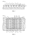
- FIG. 1 and FIG. 2 illustrate a vertical cross-section and a top view, respectively, of a Hall sensor 10 according to an exemplary embodiment of the present invention, wherein the Hall sensor 10 has six well contacts 14 and five buffer regions 19 interleaved with, and thus distributed in between, the well contacts 14, one buffer region 19 in between every two neighboring well contacts 14.
- Embodiments of the present invention are not limited to this number of well contacts 14 and buffer regions 19.
- the well contacts 14 and the buffer regions 19 are arranged such that an array of alternating well contacts 14 and buffer regions 19 is obtained.
- the first, third, fourth and sixth may be supply contacts, and the second and fifth may be sense contacts. It can be seen that in this case the central supply contact consists of the third and fourth well contact, and thus is implemented as a distributed contact. This, however, is not intended to be limiting for the present invention.
- the depth dimension of the buffer regions 19, in a direction perpendicular to the surface of the substrate 13, is such that they are extending deeper into the electrically conductive well 12 than the well contacts 14.
- Such buffer regions are further called "deep buffer regions".
- the depth of the deep buffer regions 19 might for example be 1.0 ⁇ m in case of a conductive well 12 with a depth between 3 and 4 ⁇ m.
- the width (w in FIG. 2 ) of the buffer regions is between 6 and 10 ⁇ m, more preferably between 7 and 9 ⁇ m, more preferably 8 ⁇ m. In embodiments of the present invention the width (w in FIG.
- the outer well contacts 14 are larger than the inner well contacts 14.
- the distance between the center of a well contact 14 and the closest edge of the neighboring buffer region 19 is between 1 and 4 ⁇ m, more preferably between 1.5 and 3 ⁇ m, more preferably between 1.5 and 2 ⁇ m, more preferably about 2 ⁇ m.
- 2 x w 1 has almost the same size as the depth of the conductive well 12, which may be for instance between 3 and 4 ⁇ m.
- the width w of the buffer region 19 is about 4 x w 1 .
- the width of a well contact 14 ranges between 0.2 ⁇ m and 1.0 ⁇ m, preferably between 0.4 ⁇ m and 0.7 ⁇ m.
- the spacing between two neighboring well contacts 14, from the middle of one well contact 14 towards the middle of the neighboring well contact 14 minus the width of the buffer region 19 in between both contacts varies between 2 and 4 ⁇ m, preferably between 3 and 4 ⁇ m. This distance is referred to as the "effective distance".
- the buffer width is subtracted because it does not significantly contribute to the resistance of the path between the two neighboring well contacts.
- the region through which the electrons or holes, depending on the first conductivity type, travel over the "effective distance" i.e. the region between the well contact and the buffer region
- the depth of the well 12 has a similar depth as the effective distance between two neighboring well contacts 14. This has as advantage that it results in the best trade-off between accuracy and sensitivity. The ideal well depth would be infinite though.
- the width of a buffer region 19 is preferably about twice the effective distance between two neighboring well contacts 14.
- the distance between two neighboring well contacts 14 ranges between 1 and 10 ⁇ m.
- the semiconductor chip 10 comprises 4 well contacts 14.
- Such a semiconductor chip 10 can be electrically represented as a Wheatstone bridge.
- the well contacts 14 are configured to alternatingly function during spinning as current injection contacts and as voltage measurement contacts.
- the well contacts indicated S1 and S2 are the sense contacts or voltage measurement contacts while the other two contacts are the supply or current injection contacts.
- the arrows indicate currents.
- the offset error of a Hall measurement can be cancelled out by the spinning method.
- the well contacts may be mapped in 4 separate groups of connected well contacts using a modulo 4 mapping. It is an advantage of embodiments of the present invention that the resistance value between each of these groups can be made equal.
- the maximum difference between resistance sizes is below 1% of the average resistance value, preferably below 0.1% of the average resistance value.
- a vertical Hall element typically has a difference in resistance sizes between 1% and 0.1% resulting in an offset reduction by a factor of 5 to 10 by the spinning technique, whereas in horizontal Hall sensors the spinning technique can result in a offset reduction with a factor 100 or more.
- the buffer regions create zones of equal potential within the conductive well 12 of the sensor.
- the buffer regions create a geometrical and electrical symmetry of the sense contacts S1 and S2 with respect to the supply contacts.
- each buffer region 19 is provided in between two well contacts 14
- each well contact 14 is provided in between two buffer regions 19.
- embodiments of the present invention may comprise at least one buffer region 19 outside the outer well contacts 14.
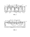
- the embodiment illustrated in FIG. 3 has two buffer regions outside the outer well contacts 14.
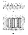
- FIG. 5 and FIG.6 schematically illustrate a vertical cross-section and a top view, respectively, of a Hall sensor 10 according to another embodiment of the present invention, comprising buffer regions 19 in between well contacts 14.
- the Hall sensor 10 illustrated has six well contacts 14 and five buffer regions 19 distributed in between the well contacts 14, one buffer region 19 in between every two neighboring well contacts 14.
- the buffer regions 19 and well contacts 14 are arranged in an array of alternating well contacts 14 and buffer regions 19.
- FIG. 4 shows a cross-section of an exemplary embodiment of the present invention comprising buffer regions 19.
- four well contacts 14 are provided, and five buffer regions 19.
- the well contacts and buffer regions are laid out in an array of alternating buffer regions and well contacts, there being a well contact in between every two neighboring buffer regions 19.
- the buffer regions 19 create a geometrical and electrical symmetry of the sense contacts S1 and S2 with respect to the supply contacts.
- the well contacts 14 are extended using well contact extensions 31.
- the well contact extensions 31 have the first conductivity type.
- the well contact extensions are formed in an additional independent process step.
- the extensions have a doping level between 1e17 and 1e18, and a depth between 1 and 2 ⁇ m.
- FIG. 7 illustrates a vertical cross-section of an exemplary embodiment of the present invention comprising well contact extensions 31.
- FIG. 8 illustrates the top view of the same exemplary embodiment.
- the buffer regions 19 neighboring the outer well contacts 14 at both sides thereof form one entire buffer region 120 surrounding the outer well contact 14.
- the buffer regions 19 also the surrounding buffer regions 120 are considered.
- the buffer regions 19 neighboring the outer well contacts 14 form one entire buffer region 120 per outer well contact.
- the distance (w 3 in FIG. 10 ) from the edge of the surrounding buffer 120 region towards the nearest edge of the surrounded well contact should be close to half of the buffer width w between the inner contacts (e.g.
- the distance (w 4 in FIG. 10 ) between the nearest edge of the surrounding buffer region 120 towards the center of the nearest well contact is equal to or slightly smaller than w 1 (the distance between the center of a well contact 14 and the closest edge of the neighboring buffer region 19).
- the distance w 4 might for example be 10% smaller than w 1 .
- the distance w 4 might for example be less than 0.1 ⁇ m smaller than w 1 .
- the distance w 4 might be between 1 and 3 ⁇ m, preferably around 2 ⁇ m.
- the outer well contacts 14 are also referred to as the symmetrization well contacts.
- the outer symmetrization well contacts enable the same current path between the second and fifth well contact through the first and sixth well contact as between the second and third or third and fourth well contact.
- the path between the second and fifth well contact via the first and sixth well contact comprises:
- the width (w2 in FIG. 10 ) of the inner well contacts 14 ranges between 0.5 ⁇ m and 1 ⁇ m.
- the length of the outer well contacts 14 would ideally be infinitely long. This is, however, not required because the region below the outer well contacts is highly resistive. Therefore in embodiments of the present invention the length of the outer well contacts is between 2 ⁇ m and 3 ⁇ m.
- the exemplary embodiment illustrated in FIG. 9 and FIG. 10 is a vertical Hall sensor comprising six well contacts with in between these well contacts deep buffer regions 19.
- the outer symmetrization well contacts 14 are embedded in the outer deep buffer regions 120 to make the sensor electrically symmetrical for current flowing from left to right as explained in the previous paragraph.
- the exemplary embodiment illustrated in FIG. 11 and FIG. 12 is similar as the embodiment illustrated in FIG. 9 and FIG. 10 , except for the buffer regions which are shallow in the exemplary embodiment illustrated in FIG. 11 and FIG. 12 .
- These buffer regions 19, in the exemplary embodiment illustrated in FIG. 11 and FIG. 12 are realised with shallow trench isolation. Having shallow buffer regions has the advantage that these buffer regions may be self-aligned and that therefore no position inaccuracy occurs.
- the shallow trench isolation 131 serves as a mask for the implant step for the well contacts 14 and the buffer regions 19 because it is slightly deeper than the implant depth (e.g.
- the shallow trench isolation has a depth between 0.4 ⁇ m and 0.5 ⁇ m and the well contacts 14 and buffer regions 19 have a depth between 0.3 ⁇ m and 0.4 ⁇ m).
- FIG. 13 an exemplary embodiment of the present invention is shown wherein shallow trench isolation 131 serves as a mask for the implant step for the well contacts and the buffer regions.
- the first conductivity type e.g. n+
- the same first conductivity type (e.g. n+) implant is applied for the well contacts 14 as for the buffer regions 19. It is desired, however, for a Hall sensors to be as uniform as possible.
- the shallow buffer regions and the well contacts are formed simultaneously. Therefore the shallow buffer regions are self-aligned with the well contacts.
- polysilicon 142 may be used instead of shallow trench isolation as a mask for the implant step.
- polysilicon defines the drift region having an effective distance over which the electrons or holes, depending on the first conductivity type, drift.
- the thickness of the polysilicon is between 0.2 and 0.5 ⁇ m.
- FIG. 14 illustrates an embodiment of the present invention wherein the regions in between the well contacts 14 and the buffer regions 19 and/or the regions outside the outer buffer regions 19 or well contacts 14 are covered with a thin barrier layer, comprising dielectric material, for instance an oxide layer 141, with a polysilicon layer 142 on top.
- a thin barrier layer comprising dielectric material, for instance an oxide layer 141
- polysilicon layer 142 on top.
- the advantage of polysilicon is that substantially less interface states are present compared to shallow trench isolation where interface states are caused by impurities between the STI oxide 131 and the semiconductor interface.
- polysilicon when using polysilicon as drift region it is important that the polysilicon is grounded because of the depletion region which affects the symmetry in the Hall sensor.
- the depletion region is strongly bias dependent and its size is different for a high voltage contact (e.g. 2 V) compared to for a low voltage contact (e.g. 0 V).
- the buffer regions 19 may be electrically interconnected. In embodiments according to the present invention, the buffer regions 19 are floating.
- the distance between centers of neighboring buffer regions 19 is the same for all neighboring buffer regions 19. This is for example the case in the embodiment illustrated in FIG. 3 and FIG. 4 . This is required for having electrical symmetry. In embodiments of the present invention the distance between neighboring buffer regions 19 ranges between 2 ⁇ m and 6 ⁇ m, preferably between 3 ⁇ m and 5 ⁇ m.
- the distance between centers of neighboring buffer regions 19 is larger between buffer regions located at extremities of the array of buffer regions than between buffer regions located at the center thereof. This is for example illustrated in the embodiments illustrated in FIG. 1 , FIG. 5 , FIG. 7 , FIG. 9 , and FIG. 11 .
- the total buffer width between two neighboring well contacts is equal. This also holds for the second and fifth well contacts via the first and sixth well contact in case of a semiconductor chip with six well contacts.
- the width w, depth d and length (perpendicular to width and depth) dimensions of a buffer region 19 are the same for all buffer regions 19. This is for instance illustrated in the embodiment of FIG. 3 and FIG. 4 .
- some buffer regions 19 may have other dimensions than other buffer regions.
- the first and last buffer regions 19 in the array of buffer regions have a larger width dimension.
- the distance between neighboring well contacts 14 is the same for all neighboring well contacts 14. This is for instance illustrated in the embodiments of FIG. 3 and FIG. 4 . It is an advantage of embodiments of the present invention that electrical symmetry can be realized through geometrical symmetry. In embodiments of the present invention the distance between neighboring well contacts 14 ranges between 10 ⁇ m and 14 ⁇ m, preferably between 11 ⁇ m and 13 ⁇ m.
- the distance between neighboring well contacts 14 is larger between well contacts located at extremities of the array of well contacts than between well contacts located at the center thereof. This is for example illustrated in the embodiments illustrated in FIG. 1 , FIG. 5 , FIG. 7 , FIG. 9 , and FIG. 11 .
- a well contact 14 In embodiments of the present invention the dimensions of a well contact 14 are the same for all well contacts 14, as illustrated in all embodiments in the drawings. The present invention, however, is not limited thereto, and different well contacts could have different dimensions.
- the length of the well contacts 14 is larger than the length of the buffer regions 19.
- the width of the buffer regions 19 is wider than the width of the well contacts.
- the width of the buffer regions 19 is such that the total current from a well contact 14 passes through (one of) the buffer regions 19 neighboring the well contact 14.
- the supply contacts may be configured for being current driven or voltage driven.
- embodiments of the present invention relate to a method for manufacturing a semiconductor chip 10 for measuring a magnetic field based on the Hall effect.
- the semiconductor chip 10 is a vertical Hall sensor comprising well contacts 14 and buffer regions 19 in an electrically conductive well 12.
- the electrically conductive well 12 has a first conductivity type and is embedded in a substrate 13 having the second conductivity type.
- the well contacts 14 and buffer regions 19 have the first conductivity type.
- the method comprises at least one processing step for applying the well contacts and the buffer regions 19. In embodiments of the present invention applying the well contacts 14 and the buffer regions 19 is done simultaneously during the same processing step(s). Therefore it is not required to add any additional processing steps when adding the buffer regions 19 to the vertical Hall sensor.
- the method for manufacturing a semiconductor chip 10 for measuring a magnetic field based on the Hall effect may comprise a first step wherein shallow trench isolation is applied. In a following step a first conductivity type implant is applied on the regions not covered by the shallow trench isolation.
- the method for manufacturing a semiconductor chip 10 comprises a first step wherein a thin barrier layer, for instance a thin oxide layer 141, is applied.
- the applied oxide layer may be smaller than 1 ⁇ m, preferably smaller than 0.1 ⁇ m, more preferably smaller than 0.04 ⁇ m.
- a polysilicon layer 142 is applied on top of the thin barrier layer, and selectively removed at locations where an implant is to be applied.
- the barrier layer 141 is removed, for instance etched away, in the regions not covered by polysilicon.
- a first conductivity type implant is applied on the substrate, and implantation actually takes place only on the regions not covered by the polysilicon. This way, a self-aligned process is carrier out.
Landscapes
- Physics & Mathematics (AREA)
- Condensed Matter Physics & Semiconductors (AREA)
- General Physics & Mathematics (AREA)
- Engineering & Computer Science (AREA)
- Manufacturing & Machinery (AREA)
- Hall/Mr Elements (AREA)
- Measuring Magnetic Variables (AREA)
Abstract
Description
- The present invention relates to the field of vertical Hall sensors. More specifically, it relates to a system with limited, e.g. reduced, offset error for measuring a magnetic field and to a method for manufacturing such system.
- Vertical Hall sensors have the advantage that they can be manufactured using conventional semiconductor technology (e.g. CMOS). They have, however, the disadvantage that they suffer from a relatively high offset voltage compared to horizontal Hall sensors. The offset voltage is the voltage measured when no magnetic field is present.
- The measurement error due to offset voltage can be decreased by several techniques, such as for instance the spinning current technique. In this technique, the supply and readout contacts are cyclically interchanged. In one phase the offset is then added to the magnetic signal with positive sign and in the other phase with negative sign. By averaging both phases, the offset can typically be reduced more than 100 times.
- A Hall sensor may be represented as a distributed resistive Wheatstone bridge. In order for the spinning current technique to be effective it is important that electrical symmetry exists within the vertical Hall sensor (i.e. that all resistors in the resistive Wheatstone bridge have about the same value). A vertical Hall element, however, does not provide this electrical symmetry by default since all contacts are on one side and since the active area (e.g. an n-well) only has a limited depth. Therefore, in practice, rather than a factor 100, the offset is only reduced by a factor 5-10 after applying the spinning current technique. Moreover, the residual offset is temperature dependent and the dependency is non-linear. This requires a time consuming calibration procedure.
-
EP1540748 discloses a magnetic field sensor with a Hall element that has two inner and two outer contacts arranged along a straight line. The contacts are arranged on the surface of a well of a first conductivity type embedded in a substrate of a second conductivity type. A first of the two outer contacts and a first of the two inner contacts which are not adjacent contacts act as supply contacts to which a current can be applied, and the second of the two outer contacts and the second of the two inner contacts act as sense contacts for tapping a Hall voltage. A first resistance is provided between the first contact and the second contact, a second resistance is provided between the second and the third contact, a third resistance is provided between the third and the fourth contact, and a fourth resistance is provided between the first and the fourth contact. The resistance values of the first, second and third resistances are substantially equal. An additional resistance is furthermore provided, coupled in parallel to the fourth resistance, and having a resistance value selected such that the parallel resistance value of the fourth and the additional resistance is substantially equal to the resistance value of any of the first, second or third resistances. This way, the equivalent Wheatstone resistor bridge is balanced. With proper dimensioning of the additional resistor this works and can reduce to zero the residual offset after spinning. However, this works only at one fixed operation condition concerning biasing voltage and temperature. If any of these two parameters varies, the matching is disturbed by additional effects arising from the non-perfect symmetry between inside and outside contacts, leading to a strong increase of the residual offset. - The minimum magnetic flux density which can be accurately measured depends on the offset error of the vertical Hall sensor: the smaller the offset error, the more accurately a magnetic flux density can be measured. Therefore, in view of the difficulty in reducing offset errors, there is still room for improvement in vertical Hall sensors.
- It is an object of embodiments of the present invention to provide a system for sensitive and accurate magnetic field measurements based on the Hall effect. The above objective is accomplished by a method and a device according to the present invention.
- In a first aspect, the present invention provides a semiconductor chip for measuring a magnetic field based on the Hall effect. The semiconductor chip comprises:
- an electrically conductive well having a first conductivity type, in a substrate having a second conductivity type,
- at least four well contacts arranged at the surface of the well, and having the first conductivity type,
- a plurality of buffer regions interleaved with the well contacts, and having the first conductivity type.
- The buffer regions are highly conductive with a conductivity that may be ranging between 5 Ohm/sq and 100 Ohm/sq for shallow buffers and between 100 Ohm/sq and 1000 Ohm/sq for deep buffers. The buffer region dimensions are such that at least part of the current from a well contact to another well contact transits through one of its neighboring buffer regions.
- It is an advantage of embodiments of the present invention that the offset error is reduced by introducing highly conductive buffer regions through which the currents between well contacts flows. These buffer regions introduce zones of equal potential in the electrically conductive well and thereby provide an increased electrical symmetry compared to other vertical Hall sensors lacking the buffer regions. In embodiments of the present invention any current from a well contact transits through one of its neighboring buffer regions. It is an advantage of embodiments of the present invention that the surroundings of the well contacts are made equal. This "potential buffer" concept makes it irrelevant whether the current is running from one contact to its neighboring contact or from one external contact to the opposite external contact. In embodiments of the present invention the buffer regions are not electrically connected from outside the semiconductor chip. Therefore, in these embodiments, a floating self-adjusting potential exists for each buffer region. It is an advantage of embodiments of the present invention that symmetry in the sensor allows to decrease the offset voltage. In embodiments of the present invention the symmetry is increased by introducing buffer regions in between the well contacts. It is an advantage of embodiments of the present invention that electrical symmetry is realized on a single Hall element by introducing highly conductive zones in between them. When in prior art solutions multiple Hall elements are used, this has the disadvantage with regard to embodiments of the present invention that they have to be spaced further from each other to avoid connection of the wells and that the prior art solution is more sensitive for a good alignment between the contacts which could compromise good matching. It is an advantage of embodiments of the present invention that the offset error can be reduced, after spinning, with a factor between 20 and 100 independent of the temperature and biasing conditions. It is an advantage of embodiments of the present invention that they are applicable in multiple operation conditions (e.g. biasing voltage) and temperatures.
- In a semiconductor chip according to embodiments of the present invention the regions in between the well contacts and the buffer regions and/or the regions outside the outer buffer regions or well contacts are filled with dielectric material, such as oxide.
- In a semiconductor chip according to embodiments of the present invention the regions in between the well contacts and the buffer regions and/or the regions outside the outer buffer regions or well contacts are covered by a thin dielectric, for instance oxide, layer with a polysilicon layer on top.
- It is an advantage of embodiments of the present invention that the polysilicon and/or dielectric regions may serve as masking regions for the first conductivity type (e.g. n+) implant step. Through the first conductivity type (e.g. n+) implant step the well contacts and buffer regions are realized. During operation, the polysilicon or dielectric regions are the drift regions between the well contacts and buffer regions.
- A semiconductor chip according to embodiments of the present invention may comprise a buffer region outside each of the outer well contacts, wherein the buffer region outside the outer well contacts is having the first conductivity type and is highly conductive and wherein the buffer region is at least as wide as the other buffer regions and wherein the two outer buffer regions are electrically connected together on a floating potential.
- It is an advantage of embodiments of the present invention that the electrical symmetry is increased by adding highly conductive buffer regions outside the outer well contacts.
- A semiconductor chip according to embodiments of the present invention, may comprise at least six well contacts. It is an advantage of embodiments of the present invention that the electrical symmetry may be increased by having more than five well contacts.
- In a semiconductor chip according to embodiments of the present invention, the well contacts and buffer regions may be circular.
- In a semiconductor chip according to embodiments of the present invention, the distance between two neighboring buffer regions may be the same for all neighboring buffer regions and the dimensions of a buffer region may be the same for all buffer regions. It is an advantage of embodiments of the present invention that electrical symmetry can be realized through geometrical symmetry. It is an advantage of embodiments of the present invention that the electrical and geometrical symmetry is reproducible and that the process sensitivity is decreased.
- In a semiconductor chip according to embodiments of the present invention, the distance between two neighboring well contacts may be the same for all neighboring well contacts and the dimensions of a well contact are the same for all well contacts.
- In a semiconductor chip according to embodiments of the present invention, the buffer regions are extending to the same depth into the electrically conductive well as the well contacts. In embodiments according to the present invention the depth of the buffer regions may be between 2 to 3 times the depth of the electrically conductive wells. The buffer regions may be as deep as possible.
- It is an advantage of embodiments of the present invention that the buffer regions extend so deep into the electrically conductive well that a majority of the currents, for instance more than 90% of the currents, such as all currents, between the well contacts go through the buffer regions.
- In embodiments of the present invention, the buffer regions may have a width between the width of the well contacts and twice the depth of the electrically conductive well. The buffer regions may for example be between 6 and 20 times wider than the well contacts. It is an advantage of embodiments of the present invention that the buffer regions are so wide that all currents between the well contacts go through the buffer regions.
- In embodiments of the present invention, the buffer regions neighboring the outer well contacts may form one entire buffer region surrounding the outer well contact. It is an advantage of embodiments of the present invention that the electrical symmetry is increased when the outer well contacts are embedded in buffer regions.
- In a semiconductor chip according to embodiments of the present invention, the well contacts may be extended using well contact extensions having the first conductivity type. It is an advantage of embodiments of the present invention that the well contact extensions provide a contact between the well contacts, having for example a strong retrograde profile, and the deep well regions of higher conductivity.
- In a second aspect, the present invention provides a method for manufacturing a semiconductor chip, for instance a semiconductor chip according to embodiments of the present invention, suitable for measuring a magnetic field based on the Hall effect. In the method, applying the well contacts and applying the buffer regions involves the same processing step or processing steps. It is an advantage of embodiments of the present invention where shallow buffer regions are implemented, that no additional processing steps are required for implementing the buffer regions. It is an advantage of embodiments of the present invention that the shallow buffers are self-aligned with the well contacts because they are implemented in the same processing step or processing steps.
- In methods according to embodiments of the present invention, the following steps may be applied:
- in a first step shallow trench isolation is applied, and
- in a next step a first conductivity type implant is applied on the regions not covered by the shallow trench isolation.
- In methods according to embodiments of the present invention, the following steps may be applied:
- in a first step a thin dielectric layer is applied,
- in a next step polysilicon is applied over the dielectric layer,
- thereafter, the dielectric layer and the polysilicon are etched away where the well contacts and the buffer regions will later be formed, and then
- a first conductivity type implant is applied on the regions not covered by the polysilicon layer.
- Particular and preferred aspects of the invention are set out in the accompanying independent and dependent claims. Features from the dependent claims may be combined with features of the independent claims and with features of other dependent claims as appropriate and not merely as explicitly set out in the claims.
- For purposes of summarizing the invention and the advantages achieved over the prior art, certain objects and advantages of the invention have been described hereinabove. Of course, it is to be understood that not necessarily all such objects or advantages may be achieved in accordance with any particular embodiment of the invention. Thus, for example, those skilled in the art will recognize that the invention may be embodied or carried out in a manner that achieves or optimizes one advantage or group of advantages as taught herein without necessarily achieving other objects or advantages as may be taught or suggested herein.
- The above and other aspects of the invention will be apparent from and elucidated with reference to the embodiment(s) described hereinafter.
- The invention will now be described further, by way of example, with reference to the accompanying drawings, in which:
-
FIG. 1 provides a schematic vertical cross-section of a vertical Hall sensor with deep buffer regions in accordance with a first embodiment of the present invention. -
FIG. 2 provides a schematic top view of the vertical Hall sensor ofFIG. 1 with deep buffer regions in accordance with embodiments of the present invention. -
FIG. 3 provides a schematic vertical cross-section of a vertical Hall sensor with deep buffer regions in accordance with embodiments of the present invention. -
FIG.4 provides a schematic vertical cross-section of a vertical Hall sensor with wide buffer regions in accordance with embodiments of the present invention. -
FIG. 5 provides a schematic vertical cross-section of a vertical Hall sensor with wide buffer regions in accordance with embodiments of the present invention. -
FIG. 6 provides a schematic top view of the vertical Hall sensor ofFIG. 5 with wide buffer regions in accordance with embodiments of the present invention. -
FIG. 7 provides a schematic vertical cross-section of a vertical Hall sensor with deep buffer regions and well contact extensions in accordance with a second embodiment of the present invention. -
FIG. 8 provides a schematic top view of the vertical Hall sensor ofFIG. 7 with deep buffer regions and well contact extensions in accordance with embodiments of the present invention. -
FIG. 9 provides a schematic vertical cross-section of a vertical Hall sensor according to a fourth embodiment of the present invention, with deep buffer regions, and wherein the outer symmetrization well contacts lie inside the buffer regions. -
FIG. 10 provides a schematic top view of the vertical Hall sensor ofFIG. 9 with deep buffer regions, and wherein the outer symmetrization well contacts lie inside the buffer regions. -
FIG. 11 provides a schematic vertical cross-section of a vertical Hall sensor according to a fifth embodiment of the present invention, with shallow buffer regions, and wherein the outer symmetrization well contacts lie inside the buffer regions. -
FIG. 12 provides a schematic top view of the vertical Hall sensor ofFIG. 11 with shallow buffer regions, and wherein the outer symmetrization well contacts lie inside the buffer regions.
The drawings are only schematic and are non-limiting. In the drawings, the size of some of the elements may be exaggerated and not drawn on scale for illustrative purposes. The dimensions and the relative dimensions do not necessarily correspond to actual reductions to practice of the invention. -
FIG. 13 provides a schematic vertical cross-section of a vertical Hall sensor whereinshallow trench isolation 131 serves as a mask for the implant step for the well contacts and the buffer regions in accordance with embodiments of the present invention. -
FIG. 14 provides a schematic vertical cross-section of a vertical Hall sensor wherein the regions in between the well contacts and the buffer regions and/or wherein the regions outside the outer buffer regions or well contacts are covered by a thin oxide layer with a polysilicon layer on top. - Any reference signs in the claims shall not be construed as limiting the scope.
- In the different drawings, the same reference signs refer to the same or analogous elements.
- The present invention will be described with respect to particular embodiments and with reference to certain drawings but the invention is not limited thereto but only by the claims. The drawings described are only schematic and are non-limiting. In the drawings, the size of some of the elements may be exaggerated and not drawn on scale for illustrative purposes. The dimensions and the relative dimensions do not correspond to actual reductions to practice of the invention.
- The terms first, second and the like in the description and in the claims, are used for distinguishing between similar elements and not necessarily for describing a sequence, either temporally, spatially, in ranking or in any other manner. It is to be understood that the terms so used are interchangeable under appropriate circumstances and that the embodiments of the invention described herein are capable of operation in other sequences than described or illustrated herein.
- Moreover, the terms top, under and the like in the description and the claims are used for descriptive purposes and not necessarily for describing relative positions. It is to be understood that the terms so used are interchangeable under appropriate circumstances and that the embodiments of the invention described herein are capable of operation in other orientations than described or illustrated herein.
- It is to be noticed that the term "comprising", used in the claims, should not be interpreted as being restricted to the means listed thereafter; it does not exclude other elements or steps. It is thus to be interpreted as specifying the presence of the stated features, integers, steps or components as referred to, but does not preclude the presence or addition of one or more other features, integers, steps or components, or groups thereof. Thus, the scope of the expression "a device comprising means A and B" should not be limited to devices consisting only of components A and B. It means that with respect to the present invention, the only relevant components of the device are A and B.
- Reference throughout this specification to "one embodiment" or "an embodiment" means that a particular feature, structure or characteristic described in connection with the embodiment is included in at least one embodiment of the present invention. Thus, appearances of the phrases "in one embodiment" or "in an embodiment" in various places throughout this specification are not necessarily all referring to the same embodiment, but may. Furthermore, the particular features, structures or characteristics may be combined in any suitable manner, as would be apparent to one of ordinary skill in the art from this disclosure, in one or more embodiments.
- Similarly it should be appreciated that in the description of exemplary embodiments of the invention, various features of the invention are sometimes grouped together in a single embodiment, figure, or description thereof for the purpose of streamlining the disclosure and aiding in the understanding of one or more of the various inventive aspects. This method of disclosure, however, is not to be interpreted as reflecting an intention that the claimed invention requires more features than are expressly recited in each claim. Rather, as the following claims reflect, inventive aspects lie in less than all features of a single foregoing disclosed embodiment. Thus, the claims following the detailed description are hereby expressly incorporated into this detailed description, with each claim standing on its own as a separate embodiment of this invention.
- Furthermore, while some embodiments described herein include some but not other features included in other embodiments, combinations of features of different embodiments are meant to be within the scope of the invention, and form different embodiments, as would be understood by those in the art. For example, in the following claims, any of the claimed embodiments can be used in any combination.
- It should be noted that the use of particular terminology when describing certain features or aspects of the invention should not be taken to imply that the terminology is being re-defined herein to be restricted to include any specific characteristics of the features or aspects of the invention with which that terminology is associated.
- In the description provided herein, numerous specific details are set forth. However, it is understood that embodiments of the invention may be practiced without these specific details. In other instances, well-known methods, structures and techniques have not been shown in detail in order not to obscure an understanding of this description.
- Where in embodiments of the present invention reference is made to the "depth" of the well contact or of the buffer region the depth is measured in a direction orthogonal to the substrate surface.
- Where in embodiments of the present invention reference is made to the "length" of the well contact or of the buffer region the length is measured orthogonal to the depth direction and along the length of the well contact or of the buffer region.
- Where in embodiments of the present invention reference is made to the "width" of the well contact or of the buffer region, the width is measured orthogonal to the depth direction and orthogonal to the length direction.
- Where in embodiments of the present invention reference is made to the "outer well contacts", reference is made to the two outer well contacts of an array of substantially parallel well contacts. Hereby the well contacts are elongated well contacts and they are parallel in their elongated direction. All the other well contacts are the inner well contacts.
- In a first aspect, the present invention relates to a
semiconductor chip 10 for measuring a magnetic field based on the Hall effect. - According to embodiments of the present invention, the
semiconductor chip 10 for measuring a magnetic field based on the Hall effect, also called a Hall sensor in this description, comprises an electricallyconductive well 12 having a first conductivity type, in asubstrate 13 having a second conductivity type. In embodiments of the present invention, without being limited thereto, the first conductivity type of the electricallyconductive well 12 is n-type whereas the second conductivity type of thesubstrates 13 is p-type. In embodiments of the present invention the doping level of the p-type substrate 13 is about 1e15. In embodiments of the present invention the doping level of the n-type well 12 is between 1e16 and 5e16. The profile of the doping level maybe constant or increasing with the depth (i.e. retrograde). - The
semiconductor chip 10 furthermore comprises at least fourwell contacts 14 arranged at the surface of the well 12 which have the first conductivity type, n-type in the example given above. Thesemiconductor chip 10 may have an even well contact count or an odd well contact count. - When having four well contacts only an electrically non-symmetrical configuration can be obtained. In a symmetrical Hall configuration all resistors in the resistive Wheatstone bridge have a similar value.
- In case of an even number of at least six well contacts, the number being (N x 4 + 2) (e.g. 6, 10, 14, 18), the well contacts may be arranged in N groups of 4 contacts. When having an even number of at least six well contacts, the outer well contacts may be connected by a metal line which is left floating (non-biased outer well contacts). In the case of at least six well contacts, all well contacts except for the outer ones may be grouped in groups of four well contacts. The first well contacts of each group may be electrically interconnected, the second well contacts of each group may be electrically interconnected, the third well contacts of each group may be electrically interconnected and the fourth well contacts of each group may be electrically interconnected. For example when numbering the 16 inner well contacts of a group of 18 well contacts consecutively this results in a first group (1-4), a second group (5-8), a third group (9-12), and a fourth group (13-16). The outer well contacts of the configuration may be electrically interconnected and the first well contacts (1,5,9,13) of each group may be electrically interconnected, and the second well contacts (2,6,10,14) of each group may be electrically interconnected etc.
- In embodiments of the present invention the
well contacts 14 are interconnected to result in four groups of well contacts independent of the total number of well contacts. In the examples below the contacts are numbered consecutively. - In a sensor with five well contacts, the first and fifth well contacts might be interconnected.
- In a sensor with 9 well contacts, well contacts 1-5-9, 2-6, 3-7, 4-8 might be interconnected.
- In a sensor with 17 well contacts, well contacts 1-5-9-13-17, 2-6-10-14, 3-7-11-15, 4-8-12-16 might be interconnected.
- In these embodiments the first well contact is connected with the nx4+1 well contact(s), the second well contact is connected with the nx4+2 well contacts, the third well contact is connected with the nx4+3 well contacts, and the fourth well contact is connected with the nx4+4 well contacts (as long as well contacts are present). Hereby n is an integer ranging from 1 to N whereby Nx4 is smaller than or equal to the number of well contacts and (N+1)x4 is bigger than the number of well contacts. This mapping will be referred to as modulo 4 mapping.
- The
well contacts 14 may be elongated strips of conductive material on or in the surface of the well 12, arranged adjacent one another. Thewell contacts 14 may be located substantially parallel to one another in their elongated direction. This way, an array ofwell contacts 14 is provided of which twowell contacts 14 are outer well contacts, and all the other ones are inner well contacts. At least two of thewell contacts 14, in use, function as supply contacts for receiving current and injecting it into the well 12, while at least two of thewell contacts 14, in use, function as sense contacts to deliver a sense signal representative for a measured magnetic field. A plurality ofbuffer regions 19 is provided in between thewell contacts 14, and optionally also outside the region where the outer well contacts are provided. Thesebuffer regions 19 are conductive regions. Thebuffer regions 19 may be semiconductive regions also having the first conductivity type, n-type in the example given above. In embodiments of the present invention the buffer regions may be metallic. Thebuffer regions 19 are highly conductive with a conductivity that may be ranging between 5 Ohm/sq and 100 Ohm/sq for shallow buffers and with a conductivity that may be ranging 100 Ohm/sq and 1000 Ohm/sq for deep buffers. and their dimensions are such that at least part of the current from awell contact 14 to another, for instance a neighboring, well contact 14 transits through one of its neighboringbuffer regions 19. - In use, an unknown magnetic field may be applied perpendicular to the surface of the
chip 10. A bias current is injected into theconductive well 12 from acentral well contact 14, and is symmetrically collected by ground terminals at the left and right hand sides of the device. The current path goes down from the central terminal, and reaches across thechip 10 and back up to the ground terminals. - By introducing the
buffer regions 19 in thesemiconductor chip 10, interleaved with the well contacts, geometrical and electrical symmetry is created in the resistance values between thewell contacts 14. Therefore it is an advantage of embodiments of the present invention that the residual offset error of the vertical Hall element can be reduced by applying a spinning current method. When applying spinning, the well contacts are configured to alternatingly function as supply contacts for current injection and as sense contacts for voltage sensing. Because of the electrical symmetry the offset error can be eliminated by processing the subsequent measurement results. Because of the geometrical symmetry, the electrical symmetry can be maintained for a wide range of bias and temperature conditions (for example a temperature ranging from -50°C to 200°C and a bias between 1 V and 4 V). -
FIG. 1 and FIG. 2 illustrate a vertical cross-section and a top view, respectively, of aHall sensor 10 according to an exemplary embodiment of the present invention, wherein theHall sensor 10 has sixwell contacts 14 and fivebuffer regions 19 interleaved with, and thus distributed in between, thewell contacts 14, onebuffer region 19 in between every two neighboring wellcontacts 14. Embodiments of the present invention, however, are not limited to this number ofwell contacts 14 andbuffer regions 19. Thewell contacts 14 and thebuffer regions 19 are arranged such that an array of alternating wellcontacts 14 andbuffer regions 19 is obtained. Of the well contacts 25, for instance the first, third, fourth and sixth may be supply contacts, and the second and fifth may be sense contacts. It can be seen that in this case the central supply contact consists of the third and fourth well contact, and thus is implemented as a distributed contact. This, however, is not intended to be limiting for the present invention. - In the exemplary embodiment of
FIG. 1 and FIG. 2 , the depth dimension of thebuffer regions 19, in a direction perpendicular to the surface of thesubstrate 13, is such that they are extending deeper into the electrically conductive well 12 than thewell contacts 14. Such buffer regions are further called "deep buffer regions". The depth of thedeep buffer regions 19 might for example be 1.0 µm in case of aconductive well 12 with a depth between 3 and 4 µm. In embodiments of the present invention the width (w inFIG. 2 ) of the buffer regions is between 6 and 10 µm, more preferably between 7 and 9 µm, more preferably 8 µm. In embodiments of the present invention the width (w inFIG. 2 ) of a shallow highly doped buffer region is about two times the depth of theconductive well 12. In embodiments of the present invention the outer well contacts 14 (the symmetrization contacts) are larger than theinner well contacts 14. In embodiments of the present invention the distance between the center of awell contact 14 and the closest edge of the neighboring buffer region 19 (w1 inFIG. 2 ) is between 1 and 4 µm, more preferably between 1.5 and 3 µm, more preferably between 1.5 and 2 µm, more preferably about 2 µm. In embodiments of the present invention 2 x w1 has almost the same size as the depth of theconductive well 12, which may be for instance between 3 and 4 µm. In embodiments of the present invention the width w of thebuffer region 19 is about 4 x w1. In embodiments of the present invention the width of a well contact 14 (w2 inFIG. 2 ) ranges between 0.2µm and 1.0µm, preferably between 0.4µm and 0.7µm. - In embodiments of the present invention the spacing between two neighboring well
contacts 14, from the middle of onewell contact 14 towards the middle of the neighboring well contact 14 minus the width of thebuffer region 19 in between both contacts varies between 2 and 4 µm, preferably between 3 and 4 µm. This distance is referred to as the "effective distance". The buffer width is subtracted because it does not significantly contribute to the resistance of the path between the two neighboring well contacts. The region through which the electrons or holes, depending on the first conductivity type, travel over the "effective distance" (i.e. the region between the well contact and the buffer region) is also called the drift region. In embodiments of the present invention the depth of the well 12 has a similar depth as the effective distance between two neighboring wellcontacts 14. This has as advantage that it results in the best trade-off between accuracy and sensitivity. The ideal well depth would be infinite though. In embodiments of the present invention the width of abuffer region 19 is preferably about twice the effective distance between two neighboring wellcontacts 14. - In embodiments of the present invention the distance between two neighboring well
contacts 14 ranges between 1 and 10 µm. - In another exemplary embodiment, illustrated in
FIG.3 , thesemiconductor chip 10 comprises 4well contacts 14. Such asemiconductor chip 10 can be electrically represented as a Wheatstone bridge. Thewell contacts 14 are configured to alternatingly function during spinning as current injection contacts and as voltage measurement contacts. In the configuration illustrated inFIG. 3 , the well contacts indicated S1 and S2 are the sense contacts or voltage measurement contacts while the other two contacts are the supply or current injection contacts. In the configuration illustrated inFIG. 3 , the arrows indicate currents. - If the four resistance values in the Wheatstone bridge, formed by the semiconductor material in between two neighboring well
contacts 14, are of about equal size, the offset error of a Hall measurement can be cancelled out by the spinning method. As explained above the well contacts may be mapped in 4 separate groups of connected well contacts using a modulo 4 mapping. It is an advantage of embodiments of the present invention that the resistance value between each of these groups can be made equal. The maximum difference between resistance sizes is below 1% of the average resistance value, preferably below 0.1% of the average resistance value. A vertical Hall element typically has a difference in resistance sizes between 1% and 0.1% resulting in an offset reduction by a factor of 5 to 10 by the spinning technique, whereas in horizontal Hall sensors the spinning technique can result in a offset reduction with a factor 100 or more. - In a prior art solution as disclosed in
EP2546670 , the difference between resistance values in a vertical Hall sensor is reduced by electrically isolating the well contacts and afterwards reconnecting them. It is an advantage of embodiments of the present invention that it is not required to electrically isolate thewell contacts 14, as electrically isolating thewell contacts 14 requires more space compared to embodiments of the present invention. Typically 30 % less space will be required. Moreover, embodiments of the present invention are less sensitive to alignment errors. - The buffer regions (e.g. in
FIG. 1, FIG. 2 ,FIG. 3, FIG. 4 ) create zones of equal potential within theconductive well 12 of the sensor. The buffer regions create a geometrical and electrical symmetry of the sense contacts S1 and S2 with respect to the supply contacts. - While in the embodiment illustrated in
FIG. 1 and FIG. 2 eachbuffer region 19 is provided in between twowell contacts 14, in the embodiment illustrated inFIG. 3 each well contact 14 is provided in between twobuffer regions 19. Hence embodiments of the present invention may comprise at least onebuffer region 19 outside theouter well contacts 14. The embodiment illustrated inFIG. 3 has two buffer regions outside theouter well contacts 14. -
FIG. 5 and FIG.6 schematically illustrate a vertical cross-section and a top view, respectively, of aHall sensor 10 according to another embodiment of the present invention, comprisingbuffer regions 19 in betweenwell contacts 14. TheHall sensor 10 illustrated has sixwell contacts 14 and fivebuffer regions 19 distributed in between thewell contacts 14, onebuffer region 19 in between every two neighboring wellcontacts 14. Thebuffer regions 19 andwell contacts 14 are arranged in an array of alternating wellcontacts 14 andbuffer regions 19. - Also
FIG. 4 shows a cross-section of an exemplary embodiment of the present invention comprisingbuffer regions 19. In this embodiment, fourwell contacts 14 are provided, and fivebuffer regions 19. The well contacts and buffer regions are laid out in an array of alternating buffer regions and well contacts, there being a well contact in between every two neighboringbuffer regions 19. Also In the exemplary embodiment illustrated inFIG. 4 thebuffer regions 19 create a geometrical and electrical symmetry of the sense contacts S1 and S2 with respect to the supply contacts. - In embodiments of the present invention, the
well contacts 14 are extended using well contactextensions 31. Thewell contact extensions 31 have the first conductivity type. In embodiments according to the present invention the well contact extensions are formed in an additional independent process step. In embodiments according to the present invention the extensions have a doping level between 1e17 and 1e18, and a depth between 1 and 2 µm.FIG. 7 illustrates a vertical cross-section of an exemplary embodiment of the present invention comprising well contactextensions 31.FIG. 8 illustrates the top view of the same exemplary embodiment. - In embodiments of the present invention the
buffer regions 19 neighboring theouter well contacts 14 at both sides thereof form oneentire buffer region 120 surrounding theouter well contact 14. When in embodiments of the present invention reference in general is made to bufferregions 19 also the surroundingbuffer regions 120 are considered. In an exemplary embodiment of which the cross-section is illustrated inFIG. 9 and the top view inFIG. 10 , thebuffer regions 19 neighboring theouter well contacts 14 form oneentire buffer region 120 per outer well contact. In embodiments of the present invention the distance (w3 inFIG. 10 ) from the edge of the surroundingbuffer 120 region towards the nearest edge of the surrounded well contact should be close to half of the buffer width w between the inner contacts (e.g. 0.4 w <w3< 0.6 w or more preferably 0.45 w <w3< 0.55 w). In embodiments of the present invention the distance (w4 inFIG. 10 ) between the nearest edge of the surroundingbuffer region 120 towards the center of the nearest well contact is equal to or slightly smaller than w1 (the distance between the center of awell contact 14 and the closest edge of the neighboring buffer region 19). The distance w4 might for example be 10% smaller than w1. The distance w4 might for example be less than 0.1 µm smaller than w1. The distance w4 might be between 1 and 3 µm, preferably around 2 µm. Theouter well contacts 14 are also referred to as the symmetrization well contacts. They are electrically connected to one another, and make sure that the current does not feel any difference between going from one well contact to a neighboring well contact, and going from a well contact at one edge of the sensor to a well contact at the other edge of the sensor. For example in an embodiment with 6 well contacts (numbered consecutively), the outer symmetrization well contacts enable the same current path between the second and fifth well contact through the first and sixth well contact as between the second and third or third and fourth well contact. In this example the path between the second and fifth well contact via the first and sixth well contact comprises: - firstly a drift region over a width w4 which is preferably equal to or slightly smaller than w1,
- secondly a buffer region with a width w3 which is preferably equal to or slightly smaller than 0.5w,
- thirdly a metal line between the first and sixth well contact,
- fourthly a buffer region with a width w3 which is preferably equal to or slightly smaller than 0.5w
- finally a drift region over a width w4 which is preferably equal to or slightly smaller than w1.
- In embodiments of the present invention the width (w2 in
FIG. 10 ) of theinner well contacts 14 ranges between 0.5 µm and 1 µm. In embodiments of the present invention the length of theouter well contacts 14 would ideally be infinitely long. This is, however, not required because the region below the outer well contacts is highly resistive. Therefore in embodiments of the present invention the length of the outer well contacts is between 2 µm and 3 µm. The exemplary embodiment illustrated inFIG. 9 and FIG. 10 is a vertical Hall sensor comprising six well contacts with in between these well contactsdeep buffer regions 19. The outer symmetrization wellcontacts 14 are embedded in the outerdeep buffer regions 120 to make the sensor electrically symmetrical for current flowing from left to right as explained in the previous paragraph. - The exemplary embodiment illustrated in
FIG. 11 and FIG. 12 is similar as the embodiment illustrated inFIG. 9 and FIG. 10 , except for the buffer regions which are shallow in the exemplary embodiment illustrated inFIG. 11 and FIG. 12 . Thesebuffer regions 19, in the exemplary embodiment illustrated inFIG. 11 and FIG. 12 , are realised with shallow trench isolation. Having shallow buffer regions has the advantage that these buffer regions may be self-aligned and that therefore no position inaccuracy occurs. In embodiments according to the present invention theshallow trench isolation 131 serves as a mask for the implant step for thewell contacts 14 and thebuffer regions 19 because it is slightly deeper than the implant depth (e.g. the shallow trench isolation has a depth between 0.4 µm and 0.5 µm and thewell contacts 14 andbuffer regions 19 have a depth between 0.3µm and 0.4 µm). InFIG. 13 an exemplary embodiment of the present invention is shown whereinshallow trench isolation 131 serves as a mask for the implant step for the well contacts and the buffer regions. In embodiments according to the present invention the first conductivity type (e.g. n+) is implanted over the total sensor area. Only when there is noshallow trench isolation 131 it reaches into the silicon and forms thewell contacts 14 andbuffer regions 19. In embodiments of the present invention the same first conductivity type (e.g. n+) implant is applied for thewell contacts 14 as for thebuffer regions 19. It is desired, however, for a Hall sensors to be as uniform as possible. - In embodiments of the present invention the following process steps apply:
- applying shallow trench isolation,
- applying a first conductivity type (e.g. n+) implant on the regions not covered by the shallow trench isolation.
- In embodiments of the present invention the shallow buffer regions and the well contacts are formed simultaneously. Therefore the shallow buffer regions are self-aligned with the well contacts.
- In embodiments of the
present invention polysilicon 142 may be used instead of shallow trench isolation as a mask for the implant step. In that case polysilicon defines the drift region having an effective distance over which the electrons or holes, depending on the first conductivity type, drift. In embodiments according to the present invention the thickness of the polysilicon is between 0.2 and 0.5 µm. Self-alignment between theshallow buffer regions 19 and thewell contacts 14 is obtained by using the same processing steps for the buffer regions and the well contacts and by using the polysilicon as a mask when doping with the first conductivity type.FIG. 14 illustrates an embodiment of the present invention wherein the regions in between thewell contacts 14 and thebuffer regions 19 and/or the regions outside theouter buffer regions 19 or wellcontacts 14 are covered with a thin barrier layer, comprising dielectric material, for instance anoxide layer 141, with apolysilicon layer 142 on top.The advantage of polysilicon is that substantially less interface states are present compared to shallow trench isolation where interface states are caused by impurities between theSTI oxide 131 and the semiconductor interface. However, when using polysilicon as drift region it is important that the polysilicon is grounded because of the depletion region which affects the symmetry in the Hall sensor. The depletion region is strongly bias dependent and its size is different for a high voltage contact (e.g. 2 V) compared to for a low voltage contact (e.g. 0 V). - In embodiments of the present invention, the
buffer regions 19 may be electrically interconnected. In embodiments according to the present invention, thebuffer regions 19 are floating. - In embodiments of the present invention, the distance between centers of neighboring
buffer regions 19 is the same for all neighboringbuffer regions 19. This is for example the case in the embodiment illustrated inFIG. 3 and FIG. 4 . This is required for having electrical symmetry. In embodiments of the present invention the distance between neighboringbuffer regions 19 ranges between 2 µm and 6 µm, preferably between 3 µm and 5µm. - In alternative embodiments, the distance between centers of neighboring
buffer regions 19 is larger between buffer regions located at extremities of the array of buffer regions than between buffer regions located at the center thereof. This is for example illustrated in the embodiments illustrated inFIG. 1 ,FIG. 5 ,FIG. 7 ,FIG. 9 , andFIG. 11 . - In embodiments of the present invention the total buffer width between two neighboring well contacts is equal. This also holds for the second and fifth well contacts via the first and sixth well contact in case of a semiconductor chip with six well contacts.
- In embodiments of the present invention, the width w, depth d and length (perpendicular to width and depth) dimensions of a
buffer region 19 are the same for allbuffer regions 19. This is for instance illustrated in the embodiment ofFIG. 3 and FIG. 4 . In alternative embodiments, somebuffer regions 19 may have other dimensions than other buffer regions. For instance in the embodiments illustrated inFIG. 1 , andFIG. 5 , the first andlast buffer regions 19 in the array of buffer regions have a larger width dimension. - In embodiments of the present invention the distance between neighboring well
contacts 14 is the same for all neighboring wellcontacts 14. This is for instance illustrated in the embodiments ofFIG. 3 and FIG. 4 . It is an advantage of embodiments of the present invention that electrical symmetry can be realized through geometrical symmetry. In embodiments of the present invention the distance between neighboring wellcontacts 14 ranges between 10 µm and 14 µm, preferably between 11 µm and 13 µm. - In alternative embodiments, the distance between neighboring well
contacts 14 is larger between well contacts located at extremities of the array of well contacts than between well contacts located at the center thereof. This is for example illustrated in the embodiments illustrated inFIG. 1 ,FIG. 5 ,FIG. 7 ,FIG. 9 , andFIG. 11 . - In embodiments of the present invention the dimensions of a
well contact 14 are the same for allwell contacts 14, as illustrated in all embodiments in the drawings. The present invention, however, is not limited thereto, and different well contacts could have different dimensions. - In embodiments of the present invention the length of the
well contacts 14 is larger than the length of thebuffer regions 19. - In embodiments of the present invention the width of the
buffer regions 19 is wider than the width of the well contacts. The width of thebuffer regions 19 is such that the total current from awell contact 14 passes through (one of) thebuffer regions 19 neighboring thewell contact 14. - In embodiments of the present invention the supply contacts may be configured for being current driven or voltage driven.
- In a second aspect, embodiments of the present invention relate to a method for manufacturing a
semiconductor chip 10 for measuring a magnetic field based on the Hall effect. In embodiments of the present invention thesemiconductor chip 10 is a vertical Hall sensor comprising wellcontacts 14 andbuffer regions 19 in an electricallyconductive well 12. The electrically conductive well 12 has a first conductivity type and is embedded in asubstrate 13 having the second conductivity type. Thewell contacts 14 andbuffer regions 19 have the first conductivity type. The method comprises at least one processing step for applying the well contacts and thebuffer regions 19. In embodiments of the present invention applying thewell contacts 14 and thebuffer regions 19 is done simultaneously during the same processing step(s). Therefore it is not required to add any additional processing steps when adding thebuffer regions 19 to the vertical Hall sensor. - In embodiments of the present invention the method for manufacturing a
semiconductor chip 10 for measuring a magnetic field based on the Hall effect may comprise a first step wherein shallow trench isolation is applied. In a following step a first conductivity type implant is applied on the regions not covered by the shallow trench isolation. - In embodiments of the present invention the method for manufacturing a
semiconductor chip 10 comprises a first step wherein a thin barrier layer, for instance athin oxide layer 141, is applied. The applied oxide layer may be smaller than 1 µm, preferably smaller than 0.1 µm, more preferably smaller than 0.04 µm. In a following step apolysilicon layer 142 is applied on top of the thin barrier layer, and selectively removed at locations where an implant is to be applied. In a following step thebarrier layer 141 is removed, for instance etched away, in the regions not covered by polysilicon. In a following step a first conductivity type implant is applied on the substrate, and implantation actually takes place only on the regions not covered by the polysilicon. This way, a self-aligned process is carrier out. - While the invention has been illustrated and described in detail in the drawings and foregoing description, such illustration and description are to be considered illustrative or exemplary and not restrictive. The foregoing description details certain embodiments of the invention. It will be appreciated, however, that no matter how detailed the foregoing appears in text, the invention may be practiced in many ways. The invention is not limited to the disclosed embodiments.
Claims (14)
- A semiconductor chip (10) for measuring a magnetic field based on the Hall effect, the semiconductor chip (10) comprising:- an electrically conductive well (12) having a first conductivity type, in a substrate (13) having a second conductivity type,- at least four well contacts (14) arranged at the surface of the well (12), and having the first conductivity type,- a plurality of buffer regions (19) interleaved with the well contacts (14), and having the first conductivity type,
wherein the buffer regions (19) are highly conductive and wherein the buffer region (19) dimensions are such that at least part of the current from a well contact (14) to another well contact (14) transits through one of its neighboring buffer regions (19). - A semiconductor chip (10) according to claim 1, wherein the regions in between the well contacts (14) and the buffer regions (19) and/or wherein the regions outside the outer buffer regions (19) or well contacts (14) are filled with oxide (131).
- A semiconductor chip (10) according to claim 1, wherein the regions in between the well contacts (14) and the buffer regions (19) and/or the regions outside the outer buffer regions (19) or well contacts (14) are covered by a thin dielectric layer (141) with a polysilicon layer (142) on top.
- A semiconductor chip (10) according to any of the previous claims, the semiconductor chip (10) comprising a buffer region (19) outside each of the outer well contacts (14) wherein the buffer region (19) outside the outer well contacts (14) is having the first conductivity type and is highly conductive and wherein the buffer region (19) outside each of the outer well contacts (14) is at least as wide as the other buffer regions (19) and wherein the two buffer regions outside each of the outer well contacts (14) are electrically connected together on a floating potential.
- A semiconductor chip (10) according to any of the previous claims, the semiconductor chip comprising at least 6 well contacts (14).
- A semiconductor chip (10) according to any of the previous claims, wherein the distance (w1) between the center of a well contact (14) and the closest edge of a neighboring buffer region (19) is between 1.5 µm and 2 µm for the inner contacts (14).
- A semiconductor chip (10) according to any of the previous claims, wherein the buffer regions (19) are extending to the same depth into the electrically conductive well (12) as the well contacts (14).
- A semiconductor chip (10) according to any of the previous claims, wherein the buffer regions (19) have a width between the width of the well contacts (14) and twice the depth of the electrically conductive well (12).
- A semiconductor chip (10) according to any of the previous claims, wherein the buffer regions (19) neighboring the outer well contacts (14) form one entire buffer region (120) surrounding the outer well contact (14).
- A semiconductor chip (10) according to claim 9, wherein the distance (w4) between the nearest edge of a surrounding buffer region (120) and the center of the nearest well contact (14) equals the distance (w1) between the center of a well contact (14) and the closest edge of a neighboring buffer region (19), or 0.1 µm or less smaller.
- A semiconductor chip (10) according to any of the previous claims, wherein the well contacts (14) are extended using well contact extensions (31) having the first conductivity type.
- A method for manufacturing a semiconductor chip (10) for measuring a magnetic field based on the Hall effect, wherein applying the well contacts (14) and applying the buffer regions (19) involves the same processing step or processing steps.
- A method for manufacturing a semiconductor chip (10) according to claim 12, wherein the method comprises the following steps:- applying shallow trench isolation,- applying a first conductivity type implant on the regions not covered by the shallow trench isolation.
- A method for manufacturing a semiconductor chip (10) according to claim 12, wherein the method comprises the following steps:- applying a thin dielectric layer (141),- applying polysilicon (142) over the dielectric layer (141),- etching away the dielectric layer (141) and the polysilicon (142) where the well contacts (14) and the buffer regions (19) will later be formed- applying a first conductivity type implant on the regions not covered by the polysilicon layer (142).
Applications Claiming Priority (1)
| Application Number | Priority Date | Filing Date | Title |
|---|---|---|---|
| GB1418662.1A GB2531536A (en) | 2014-10-21 | 2014-10-21 | Vertical hall sensors with reduced offset error |
Publications (2)
| Publication Number | Publication Date |
|---|---|
| EP3012649A1 true EP3012649A1 (en) | 2016-04-27 |
| EP3012649B1 EP3012649B1 (en) | 2018-09-19 |
Family
ID=52013327
Family Applications (1)
| Application Number | Title | Priority Date | Filing Date |
|---|---|---|---|
| EP15190681.5A Active EP3012649B1 (en) | 2014-10-21 | 2015-10-20 | Vertical hall sensors with reduced offset error |
Country Status (3)
| Country | Link |
|---|---|
| US (1) | US9543504B2 (en) |
| EP (1) | EP3012649B1 (en) |
| GB (1) | GB2531536A (en) |
Cited By (1)
| Publication number | Priority date | Publication date | Assignee | Title |
|---|---|---|---|---|
| JP2018107391A (en) * | 2016-12-28 | 2018-07-05 | エイブリック株式会社 | Semiconductor device |
Families Citing this family (8)
| Publication number | Priority date | Publication date | Assignee | Title |
|---|---|---|---|---|
| US10103320B2 (en) * | 2016-05-04 | 2018-10-16 | Tdk-Micronas Gmbh | Component with reduced stress forces in the substrate |
| US10693057B2 (en) | 2016-05-04 | 2020-06-23 | Tdk-Micronas Gmbh | Sensor component with cap over trench and sensor elements |
| CN109755381B (en) * | 2018-12-24 | 2023-08-29 | 合肥中感微电子有限公司 | Hall sensor and manufacturing method thereof |
| CN110726959B (en) * | 2019-09-11 | 2021-11-02 | 杭州电子科技大学 | A Magnetic Field Sensor with Adjustable Sensitivity Based on Anomalous Hall Effect |
| US11372061B2 (en) * | 2020-03-13 | 2022-06-28 | Globalfoundries Singapore Pte. Ltd. | Hall effect sensor devices and methods of forming hall effect sensor devices |
| CN113851582B (en) * | 2021-08-18 | 2024-09-20 | 杭州未名信科科技有限公司 | A vertical Hall sensor and its preparation method |
| TWI847082B (en) * | 2021-12-22 | 2024-07-01 | 香港商睿克科技有限公司 | Vertical hall magnetic device |
| CN119414076B (en) * | 2024-10-15 | 2025-12-05 | 太原理工大学 | A switchless, high-precision, large-range current measurement device and signal processing method |
Citations (2)
| Publication number | Priority date | Publication date | Assignee | Title |
|---|---|---|---|---|
| US5548151A (en) * | 1994-03-09 | 1996-08-20 | Kabushiki Kaisha Toshiba | Hall element for detecting a magnetic field perpendicular to a substrate |
| US20060011999A1 (en) * | 2002-09-10 | 2006-01-19 | Sentron Ag | Magnetic field sensor comprising a hall element |
Family Cites Families (7)
| Publication number | Priority date | Publication date | Assignee | Title |
|---|---|---|---|---|
| CH669068A5 (en) * | 1986-04-29 | 1989-02-15 | Landis & Gyr Ag | INTEGRATED HALL ELEMENT. |
| JP4164615B2 (en) * | 1999-12-20 | 2008-10-15 | サンケン電気株式会社 | CURRENT DETECTOR HAVING HALL ELEMENT |
| CH699933A1 (en) * | 2008-11-28 | 2010-05-31 | Melexis Technologies Sa | Vertical Hall sensor. |
| CH704689B1 (en) * | 2011-03-24 | 2016-02-29 | X Fab Semiconductor Foundries | Vertical Hall sensor and method for manufacturing a vertical Hall sensor. |
| DE102011107767A1 (en) | 2011-07-15 | 2013-01-17 | Micronas Gmbh | Hall sensor |
| US8988072B2 (en) * | 2011-07-21 | 2015-03-24 | Infineon Technologies Ag | Vertical hall sensor with high electrical symmetry |
| US9548443B2 (en) * | 2013-01-29 | 2017-01-17 | Allegro Microsystems, Llc | Vertical Hall Effect element with improved sensitivity |
-
2014
- 2014-10-21 GB GB1418662.1A patent/GB2531536A/en not_active Withdrawn
-
2015
- 2015-10-20 EP EP15190681.5A patent/EP3012649B1/en active Active
- 2015-10-21 US US14/918,704 patent/US9543504B2/en active Active
Patent Citations (2)
| Publication number | Priority date | Publication date | Assignee | Title |
|---|---|---|---|---|
| US5548151A (en) * | 1994-03-09 | 1996-08-20 | Kabushiki Kaisha Toshiba | Hall element for detecting a magnetic field perpendicular to a substrate |
| US20060011999A1 (en) * | 2002-09-10 | 2006-01-19 | Sentron Ag | Magnetic field sensor comprising a hall element |
Cited By (1)
| Publication number | Priority date | Publication date | Assignee | Title |
|---|---|---|---|---|
| JP2018107391A (en) * | 2016-12-28 | 2018-07-05 | エイブリック株式会社 | Semiconductor device |
Also Published As
| Publication number | Publication date |
|---|---|
| GB201418662D0 (en) | 2014-12-03 |
| US20160111631A1 (en) | 2016-04-21 |
| US9543504B2 (en) | 2017-01-10 |
| EP3012649B1 (en) | 2018-09-19 |
| GB2531536A (en) | 2016-04-27 |
Similar Documents
| Publication | Publication Date | Title |
|---|---|---|
| EP3012649B1 (en) | Vertical hall sensors with reduced offset error | |
| EP3039440B1 (en) | Vertical hall effect sensor | |
| CN100388523C (en) | Magnetic Field Sensors with Hall Elements | |
| KR102019514B1 (en) | Hall sensor based on semiconductor device | |
| US9063187B2 (en) | Hall sensor element and method for measuring a magnetic field | |
| EP2878940B1 (en) | MEMS pressure sensor field shield layout for surface charge immunity in oil filled packaging | |
| EP3832279B1 (en) | Semiconductor stress sensor | |
| US11205748B2 (en) | 3-contact vertical hall sensor elements connected in a ring and related devices, systems, and methods | |
| CN105223420A (en) | For the measuring method of the TFT and contact resistance that measure contact resistance | |
| US20210183849A1 (en) | Power mos device having an integrated current sensor and manufacturing process thereof | |
| US10508958B2 (en) | Semiconductor pressure sensor with piezo-resistive portions with conductive shields | |
| CN113394339B (en) | Hall effect sensor device and method of forming a Hall effect sensor device | |
| US7205622B2 (en) | Vertical hall effect device | |
| CN118483628B (en) | Magnetic sensitive element and preparation method thereof, magnetic sensitive sensor, electronic device, chip and electronic device | |
| US6510742B1 (en) | Sensor formed on silicon on insulator structure and having reduced power up drift | |
| US9304103B2 (en) | Self-calibrating ion meter | |
| JPH10270773A (en) | Hall element | |
| JP2011085557A (en) | Semiconductor sensor and method for manufacturing the same | |
| JP2004296469A (en) | Hall element | |
| CN1502126A (en) | Structure and method for determining the edge of a region in a semiconductor wafer | |
| US12035637B2 (en) | Semiconductor device with CMOS process based hall sensor and manufacturing method | |
| CN122056122A (en) | Semiconductor Hall sensor structure |
Legal Events
| Date | Code | Title | Description |
|---|---|---|---|
| PUAI | Public reference made under article 153(3) epc to a published international application that has entered the european phase |
Free format text: ORIGINAL CODE: 0009012 |
|
| AK | Designated contracting states |
Kind code of ref document: A1 Designated state(s): AL AT BE BG CH CY CZ DE DK EE ES FI FR GB GR HR HU IE IS IT LI LT LU LV MC MK MT NL NO PL PT RO RS SE SI SK SM TR |
|
| AX | Request for extension of the european patent |
Extension state: BA ME |
|
| STAA | Information on the status of an ep patent application or granted ep patent |
Free format text: STATUS: REQUEST FOR EXAMINATION WAS MADE |
|
| STAA | Information on the status of an ep patent application or granted ep patent |
Free format text: STATUS: EXAMINATION IS IN PROGRESS |
|
| 17P | Request for examination filed |
Effective date: 20161026 |
|
| RBV | Designated contracting states (corrected) |
Designated state(s): AL AT BE BG CH CY CZ DE DK EE ES FI FR GB GR HR HU IE IS IT LI LT LU LV MC MK MT NL NO PL PT RO RS SE SI SK SM TR |
|
| 17Q | First examination report despatched |
Effective date: 20161124 |
|
| GRAP | Despatch of communication of intention to grant a patent |
Free format text: ORIGINAL CODE: EPIDOSNIGR1 |
|
| STAA | Information on the status of an ep patent application or granted ep patent |
Free format text: STATUS: GRANT OF PATENT IS INTENDED |
|
| INTG | Intention to grant announced |
Effective date: 20180410 |
|
| GRAS | Grant fee paid |
Free format text: ORIGINAL CODE: EPIDOSNIGR3 |
|
| GRAA | (expected) grant |
Free format text: ORIGINAL CODE: 0009210 |
|
| STAA | Information on the status of an ep patent application or granted ep patent |
Free format text: STATUS: THE PATENT HAS BEEN GRANTED |
|
| AK | Designated contracting states |
Kind code of ref document: B1 Designated state(s): AL AT BE BG CH CY CZ DE DK EE ES FI FR GB GR HR HU IE IS IT LI LT LU LV MC MK MT NL NO PL PT RO RS SE SI SK SM TR |
|
| REG | Reference to a national code |
Ref country code: GB Ref legal event code: FG4D |
|
| REG | Reference to a national code |
Ref country code: CH Ref legal event code: EP |
|
| REG | Reference to a national code |
Ref country code: AT Ref legal event code: REF Ref document number: 1043873 Country of ref document: AT Kind code of ref document: T Effective date: 20181015 |
|
| REG | Reference to a national code |
Ref country code: IE Ref legal event code: FG4D |
|
| REG | Reference to a national code |
Ref country code: DE Ref legal event code: R096 Ref document number: 602015016541 Country of ref document: DE |
|
| REG | Reference to a national code |
Ref country code: FR Ref legal event code: PLFP Year of fee payment: 4 |
|
| REG | Reference to a national code |
Ref country code: NL Ref legal event code: MP Effective date: 20180919 |
|
| PG25 | Lapsed in a contracting state [announced via postgrant information from national office to epo] |
Ref country code: FI Free format text: LAPSE BECAUSE OF FAILURE TO SUBMIT A TRANSLATION OF THE DESCRIPTION OR TO PAY THE FEE WITHIN THE PRESCRIBED TIME-LIMIT Effective date: 20180919 Ref country code: LT Free format text: LAPSE BECAUSE OF FAILURE TO SUBMIT A TRANSLATION OF THE DESCRIPTION OR TO PAY THE FEE WITHIN THE PRESCRIBED TIME-LIMIT Effective date: 20180919 Ref country code: BG Free format text: LAPSE BECAUSE OF FAILURE TO SUBMIT A TRANSLATION OF THE DESCRIPTION OR TO PAY THE FEE WITHIN THE PRESCRIBED TIME-LIMIT Effective date: 20181219 Ref country code: GR Free format text: LAPSE BECAUSE OF FAILURE TO SUBMIT A TRANSLATION OF THE DESCRIPTION OR TO PAY THE FEE WITHIN THE PRESCRIBED TIME-LIMIT Effective date: 20181220 Ref country code: NO Free format text: LAPSE BECAUSE OF FAILURE TO SUBMIT A TRANSLATION OF THE DESCRIPTION OR TO PAY THE FEE WITHIN THE PRESCRIBED TIME-LIMIT Effective date: 20181219 Ref country code: RS Free format text: LAPSE BECAUSE OF FAILURE TO SUBMIT A TRANSLATION OF THE DESCRIPTION OR TO PAY THE FEE WITHIN THE PRESCRIBED TIME-LIMIT Effective date: 20180919 Ref country code: SE Free format text: LAPSE BECAUSE OF FAILURE TO SUBMIT A TRANSLATION OF THE DESCRIPTION OR TO PAY THE FEE WITHIN THE PRESCRIBED TIME-LIMIT Effective date: 20180919 |
|
| REG | Reference to a national code |
Ref country code: LT Ref legal event code: MG4D |
|
| REG | Reference to a national code |
Ref country code: CH Ref legal event code: PFA Owner name: X-FAB SEMICONDUCTOR FOUNDRIES GMBH, BE Free format text: FORMER OWNER: X-FAB SEMICONDUCTOR FOUNDRIES AG, BE |
|
| PG25 | Lapsed in a contracting state [announced via postgrant information from national office to epo] |
Ref country code: AL Free format text: LAPSE BECAUSE OF FAILURE TO SUBMIT A TRANSLATION OF THE DESCRIPTION OR TO PAY THE FEE WITHIN THE PRESCRIBED TIME-LIMIT Effective date: 20180919 Ref country code: HR Free format text: LAPSE BECAUSE OF FAILURE TO SUBMIT A TRANSLATION OF THE DESCRIPTION OR TO PAY THE FEE WITHIN THE PRESCRIBED TIME-LIMIT Effective date: 20180919 Ref country code: LV Free format text: LAPSE BECAUSE OF FAILURE TO SUBMIT A TRANSLATION OF THE DESCRIPTION OR TO PAY THE FEE WITHIN THE PRESCRIBED TIME-LIMIT Effective date: 20180919 |
|
| REG | Reference to a national code |
Ref country code: AT Ref legal event code: MK05 Ref document number: 1043873 Country of ref document: AT Kind code of ref document: T Effective date: 20180919 |
|
| PG25 | Lapsed in a contracting state [announced via postgrant information from national office to epo] |
Ref country code: AT Free format text: LAPSE BECAUSE OF FAILURE TO SUBMIT A TRANSLATION OF THE DESCRIPTION OR TO PAY THE FEE WITHIN THE PRESCRIBED TIME-LIMIT Effective date: 20180919 Ref country code: IT Free format text: LAPSE BECAUSE OF FAILURE TO SUBMIT A TRANSLATION OF THE DESCRIPTION OR TO PAY THE FEE WITHIN THE PRESCRIBED TIME-LIMIT Effective date: 20180919 Ref country code: PL Free format text: LAPSE BECAUSE OF FAILURE TO SUBMIT A TRANSLATION OF THE DESCRIPTION OR TO PAY THE FEE WITHIN THE PRESCRIBED TIME-LIMIT Effective date: 20180919 Ref country code: EE Free format text: LAPSE BECAUSE OF FAILURE TO SUBMIT A TRANSLATION OF THE DESCRIPTION OR TO PAY THE FEE WITHIN THE PRESCRIBED TIME-LIMIT Effective date: 20180919 Ref country code: NL Free format text: LAPSE BECAUSE OF FAILURE TO SUBMIT A TRANSLATION OF THE DESCRIPTION OR TO PAY THE FEE WITHIN THE PRESCRIBED TIME-LIMIT Effective date: 20180919 Ref country code: CZ Free format text: LAPSE BECAUSE OF FAILURE TO SUBMIT A TRANSLATION OF THE DESCRIPTION OR TO PAY THE FEE WITHIN THE PRESCRIBED TIME-LIMIT Effective date: 20180919 Ref country code: IS Free format text: LAPSE BECAUSE OF FAILURE TO SUBMIT A TRANSLATION OF THE DESCRIPTION OR TO PAY THE FEE WITHIN THE PRESCRIBED TIME-LIMIT Effective date: 20190119 Ref country code: RO Free format text: LAPSE BECAUSE OF FAILURE TO SUBMIT A TRANSLATION OF THE DESCRIPTION OR TO PAY THE FEE WITHIN THE PRESCRIBED TIME-LIMIT Effective date: 20180919 Ref country code: ES Free format text: LAPSE BECAUSE OF FAILURE TO SUBMIT A TRANSLATION OF THE DESCRIPTION OR TO PAY THE FEE WITHIN THE PRESCRIBED TIME-LIMIT Effective date: 20180919 |
|
| PG25 | Lapsed in a contracting state [announced via postgrant information from national office to epo] |
Ref country code: PT Free format text: LAPSE BECAUSE OF FAILURE TO SUBMIT A TRANSLATION OF THE DESCRIPTION OR TO PAY THE FEE WITHIN THE PRESCRIBED TIME-LIMIT Effective date: 20190119 Ref country code: SK Free format text: LAPSE BECAUSE OF FAILURE TO SUBMIT A TRANSLATION OF THE DESCRIPTION OR TO PAY THE FEE WITHIN THE PRESCRIBED TIME-LIMIT Effective date: 20180919 Ref country code: SM Free format text: LAPSE BECAUSE OF FAILURE TO SUBMIT A TRANSLATION OF THE DESCRIPTION OR TO PAY THE FEE WITHIN THE PRESCRIBED TIME-LIMIT Effective date: 20180919 |
|
| REG | Reference to a national code |
Ref country code: DE Ref legal event code: R097 Ref document number: 602015016541 Country of ref document: DE |
|
| PG25 | Lapsed in a contracting state [announced via postgrant information from national office to epo] |
Ref country code: LU Free format text: LAPSE BECAUSE OF NON-PAYMENT OF DUE FEES Effective date: 20181020 |
|
| REG | Reference to a national code |
Ref country code: IE Ref legal event code: MM4A |
|
| PLBE | No opposition filed within time limit |
Free format text: ORIGINAL CODE: 0009261 |
|
| STAA | Information on the status of an ep patent application or granted ep patent |
Free format text: STATUS: NO OPPOSITION FILED WITHIN TIME LIMIT |
|
| PG25 | Lapsed in a contracting state [announced via postgrant information from national office to epo] |
Ref country code: MC Free format text: LAPSE BECAUSE OF FAILURE TO SUBMIT A TRANSLATION OF THE DESCRIPTION OR TO PAY THE FEE WITHIN THE PRESCRIBED TIME-LIMIT Effective date: 20180919 Ref country code: DK Free format text: LAPSE BECAUSE OF FAILURE TO SUBMIT A TRANSLATION OF THE DESCRIPTION OR TO PAY THE FEE WITHIN THE PRESCRIBED TIME-LIMIT Effective date: 20180919 |
|
| 26N | No opposition filed |
Effective date: 20190620 |
|
| PG25 | Lapsed in a contracting state [announced via postgrant information from national office to epo] |
Ref country code: SI Free format text: LAPSE BECAUSE OF FAILURE TO SUBMIT A TRANSLATION OF THE DESCRIPTION OR TO PAY THE FEE WITHIN THE PRESCRIBED TIME-LIMIT Effective date: 20180919 Ref country code: IE Free format text: LAPSE BECAUSE OF NON-PAYMENT OF DUE FEES Effective date: 20181020 |
|
| PG25 | Lapsed in a contracting state [announced via postgrant information from national office to epo] |
Ref country code: MT Free format text: LAPSE BECAUSE OF NON-PAYMENT OF DUE FEES Effective date: 20181020 |
|
| PG25 | Lapsed in a contracting state [announced via postgrant information from national office to epo] |
Ref country code: TR Free format text: LAPSE BECAUSE OF FAILURE TO SUBMIT A TRANSLATION OF THE DESCRIPTION OR TO PAY THE FEE WITHIN THE PRESCRIBED TIME-LIMIT Effective date: 20180919 |
|
| PG25 | Lapsed in a contracting state [announced via postgrant information from national office to epo] |
Ref country code: MK Free format text: LAPSE BECAUSE OF NON-PAYMENT OF DUE FEES Effective date: 20180919 Ref country code: CY Free format text: LAPSE BECAUSE OF FAILURE TO SUBMIT A TRANSLATION OF THE DESCRIPTION OR TO PAY THE FEE WITHIN THE PRESCRIBED TIME-LIMIT Effective date: 20180919 Ref country code: HU Free format text: LAPSE BECAUSE OF FAILURE TO SUBMIT A TRANSLATION OF THE DESCRIPTION OR TO PAY THE FEE WITHIN THE PRESCRIBED TIME-LIMIT; INVALID AB INITIO Effective date: 20151020 |
|
| REG | Reference to a national code |
Ref country code: DE Ref legal event code: R081 Ref document number: 602015016541 Country of ref document: DE Owner name: MELEXIS TECHNOLOGIES NV, BE Free format text: FORMER OWNERS: MELEXIS TECHNOLOGIES NV, TESSENDERLO, BE; X-FAB SEMICONDUCTOR FOUNDRIES AG, 99097 ERFURT, DE Ref country code: DE Ref legal event code: R081 Ref document number: 602015016541 Country of ref document: DE Owner name: X-FAB SEMICONDUCTOR FOUNDRIES GMBH, DE Free format text: FORMER OWNERS: MELEXIS TECHNOLOGIES NV, TESSENDERLO, BE; X-FAB SEMICONDUCTOR FOUNDRIES AG, 99097 ERFURT, DE |
|
| REG | Reference to a national code |
Ref country code: BE Ref legal event code: PD Owner name: X-FAB SEMICONDUCTOR FOUNDRIES GMBH; DE Free format text: DETAILS ASSIGNMENT: CHANGE OF OWNER(S), CHANGE OF LEGAL ENTITY; FORMER OWNER NAME: X-FAB SEMICONDUCTOR FOUNDRIES AG Effective date: 20210324 |
|
| REG | Reference to a national code |
Ref country code: GB Ref legal event code: 732E Free format text: REGISTERED BETWEEN 20210624 AND 20210630 |
|
| P01 | Opt-out of the competence of the unified patent court (upc) registered |
Effective date: 20230517 |
|
| PGFP | Annual fee paid to national office [announced via postgrant information from national office to epo] |
Ref country code: BE Payment date: 20250923 Year of fee payment: 11 Ref country code: GB Payment date: 20250923 Year of fee payment: 11 |
|
| PGFP | Annual fee paid to national office [announced via postgrant information from national office to epo] |
Ref country code: FR Payment date: 20250924 Year of fee payment: 11 |
|
| REG | Reference to a national code |
Ref country code: CH Ref legal event code: U11 Free format text: ST27 STATUS EVENT CODE: U-0-0-U10-U11 (AS PROVIDED BY THE NATIONAL OFFICE) Effective date: 20251101 |
|
| PGFP | Annual fee paid to national office [announced via postgrant information from national office to epo] |
Ref country code: DE Payment date: 20250923 Year of fee payment: 11 |
|
| PGFP | Annual fee paid to national office [announced via postgrant information from national office to epo] |
Ref country code: CH Payment date: 20251101 Year of fee payment: 11 |