EP3012059A2 - Method to produce a transparent piece to be used to protect an optical component - Google Patents
Method to produce a transparent piece to be used to protect an optical component Download PDFInfo
- Publication number
- EP3012059A2 EP3012059A2 EP15186879.1A EP15186879A EP3012059A2 EP 3012059 A2 EP3012059 A2 EP 3012059A2 EP 15186879 A EP15186879 A EP 15186879A EP 3012059 A2 EP3012059 A2 EP 3012059A2
- Authority
- EP
- European Patent Office
- Prior art keywords
- piece
- mentioned
- sheet
- sheets
- pieces
- Prior art date
- Legal status (The legal status is an assumption and is not a legal conclusion. Google has not performed a legal analysis and makes no representation as to the accuracy of the status listed.)
- Granted
Links
- 238000000034 method Methods 0.000 title claims abstract description 37
- 230000003287 optical effect Effects 0.000 title claims abstract description 15
- 239000011521 glass Substances 0.000 claims abstract description 15
- 229910052594 sapphire Inorganic materials 0.000 claims abstract description 13
- 239000010980 sapphire Substances 0.000 claims abstract description 13
- 229910052710 silicon Inorganic materials 0.000 claims abstract description 12
- 239000010703 silicon Substances 0.000 claims abstract description 12
- 241000167854 Bourreria succulenta Species 0.000 claims abstract description 10
- 238000003466 welding Methods 0.000 claims abstract description 8
- 238000003754 machining Methods 0.000 claims abstract 4
- 238000002679 ablation Methods 0.000 claims description 10
- 239000002994 raw material Substances 0.000 claims description 2
- 239000000463 material Substances 0.000 abstract description 7
- 238000000608 laser ablation Methods 0.000 abstract description 2
- 238000004519 manufacturing process Methods 0.000 description 7
- 238000005520 cutting process Methods 0.000 description 5
- 230000006378 damage Effects 0.000 description 2
- 238000005530 etching Methods 0.000 description 2
- 230000002349 favourable effect Effects 0.000 description 2
- 230000000149 penetrating effect Effects 0.000 description 2
- 238000003825 pressing Methods 0.000 description 2
- 235000007173 Abies balsamea Nutrition 0.000 description 1
- 241000218685 Tsuga Species 0.000 description 1
- 230000003466 anti-cipated effect Effects 0.000 description 1
- 238000001816 cooling Methods 0.000 description 1
- 230000008642 heat stress Effects 0.000 description 1
- 238000010438 heat treatment Methods 0.000 description 1
- 238000009776 industrial production Methods 0.000 description 1
- 230000035515 penetration Effects 0.000 description 1
Images

Classifications
-
- B—PERFORMING OPERATIONS; TRANSPORTING
- B23—MACHINE TOOLS; METAL-WORKING NOT OTHERWISE PROVIDED FOR
- B23K—SOLDERING OR UNSOLDERING; WELDING; CLADDING OR PLATING BY SOLDERING OR WELDING; CUTTING BY APPLYING HEAT LOCALLY, e.g. FLAME CUTTING; WORKING BY LASER BEAM
- B23K26/00—Working by laser beam, e.g. welding, cutting or boring
- B23K26/20—Bonding
- B23K26/21—Bonding by welding
- B23K26/24—Seam welding
-
- B—PERFORMING OPERATIONS; TRANSPORTING
- B23—MACHINE TOOLS; METAL-WORKING NOT OTHERWISE PROVIDED FOR
- B23K—SOLDERING OR UNSOLDERING; WELDING; CLADDING OR PLATING BY SOLDERING OR WELDING; CUTTING BY APPLYING HEAT LOCALLY, e.g. FLAME CUTTING; WORKING BY LASER BEAM
- B23K26/00—Working by laser beam, e.g. welding, cutting or boring
- B23K26/36—Removing material
- B23K26/38—Removing material by boring or cutting
-
- B—PERFORMING OPERATIONS; TRANSPORTING
- B23—MACHINE TOOLS; METAL-WORKING NOT OTHERWISE PROVIDED FOR
- B23K—SOLDERING OR UNSOLDERING; WELDING; CLADDING OR PLATING BY SOLDERING OR WELDING; CUTTING BY APPLYING HEAT LOCALLY, e.g. FLAME CUTTING; WORKING BY LASER BEAM
- B23K26/00—Working by laser beam, e.g. welding, cutting or boring
- B23K26/20—Bonding
- B23K26/206—Laser sealing
-
- B—PERFORMING OPERATIONS; TRANSPORTING
- B23—MACHINE TOOLS; METAL-WORKING NOT OTHERWISE PROVIDED FOR
- B23K—SOLDERING OR UNSOLDERING; WELDING; CLADDING OR PLATING BY SOLDERING OR WELDING; CUTTING BY APPLYING HEAT LOCALLY, e.g. FLAME CUTTING; WORKING BY LASER BEAM
- B23K26/00—Working by laser beam, e.g. welding, cutting or boring
- B23K26/20—Bonding
- B23K26/21—Bonding by welding
- B23K26/24—Seam welding
- B23K26/244—Overlap seam welding
-
- B—PERFORMING OPERATIONS; TRANSPORTING
- B23—MACHINE TOOLS; METAL-WORKING NOT OTHERWISE PROVIDED FOR
- B23K—SOLDERING OR UNSOLDERING; WELDING; CLADDING OR PLATING BY SOLDERING OR WELDING; CUTTING BY APPLYING HEAT LOCALLY, e.g. FLAME CUTTING; WORKING BY LASER BEAM
- B23K26/00—Working by laser beam, e.g. welding, cutting or boring
- B23K26/20—Bonding
- B23K26/32—Bonding taking account of the properties of the material involved
- B23K26/324—Bonding taking account of the properties of the material involved involving non-metallic parts
-
- B—PERFORMING OPERATIONS; TRANSPORTING
- B23—MACHINE TOOLS; METAL-WORKING NOT OTHERWISE PROVIDED FOR
- B23K—SOLDERING OR UNSOLDERING; WELDING; CLADDING OR PLATING BY SOLDERING OR WELDING; CUTTING BY APPLYING HEAT LOCALLY, e.g. FLAME CUTTING; WORKING BY LASER BEAM
- B23K26/00—Working by laser beam, e.g. welding, cutting or boring
- B23K26/36—Removing material
- B23K26/361—Removing material for deburring or mechanical trimming
-
- B—PERFORMING OPERATIONS; TRANSPORTING
- B23—MACHINE TOOLS; METAL-WORKING NOT OTHERWISE PROVIDED FOR
- B23K—SOLDERING OR UNSOLDERING; WELDING; CLADDING OR PLATING BY SOLDERING OR WELDING; CUTTING BY APPLYING HEAT LOCALLY, e.g. FLAME CUTTING; WORKING BY LASER BEAM
- B23K26/00—Working by laser beam, e.g. welding, cutting or boring
- B23K26/36—Removing material
- B23K26/362—Laser etching
- B23K26/364—Laser etching for making a groove or trench, e.g. for scribing a break initiation groove
-
- B—PERFORMING OPERATIONS; TRANSPORTING
- B23—MACHINE TOOLS; METAL-WORKING NOT OTHERWISE PROVIDED FOR
- B23K—SOLDERING OR UNSOLDERING; WELDING; CLADDING OR PLATING BY SOLDERING OR WELDING; CUTTING BY APPLYING HEAT LOCALLY, e.g. FLAME CUTTING; WORKING BY LASER BEAM
- B23K26/00—Working by laser beam, e.g. welding, cutting or boring
- B23K26/50—Working by transmitting the laser beam through or within the workpiece
- B23K26/57—Working by transmitting the laser beam through or within the workpiece the laser beam entering a face of the workpiece from which it is transmitted through the workpiece material to work on a different workpiece face, e.g. for effecting removal, fusion splicing, modifying or reforming
-
- C—CHEMISTRY; METALLURGY
- C03—GLASS; MINERAL OR SLAG WOOL
- C03B—MANUFACTURE, SHAPING, OR SUPPLEMENTARY PROCESSES
- C03B23/00—Re-forming shaped glass
- C03B23/20—Uniting glass pieces by fusing without substantial reshaping
-
- C—CHEMISTRY; METALLURGY
- C03—GLASS; MINERAL OR SLAG WOOL
- C03B—MANUFACTURE, SHAPING, OR SUPPLEMENTARY PROCESSES
- C03B23/00—Re-forming shaped glass
- C03B23/20—Uniting glass pieces by fusing without substantial reshaping
- C03B23/203—Uniting glass sheets
-
- H—ELECTRICITY
- H01—ELECTRIC ELEMENTS
- H01L—SEMICONDUCTOR DEVICES NOT COVERED BY CLASS H10
- H01L31/00—Semiconductor devices sensitive to infrared radiation, light, electromagnetic radiation of shorter wavelength or corpuscular radiation and specially adapted either for the conversion of the energy of such radiation into electrical energy or for the control of electrical energy by such radiation; Processes or apparatus specially adapted for the manufacture or treatment thereof or of parts thereof; Details thereof
- H01L31/02—Details
- H01L31/0203—Containers; Encapsulations, e.g. encapsulation of photodiodes
-
- H—ELECTRICITY
- H04—ELECTRIC COMMUNICATION TECHNIQUE
- H04N—PICTORIAL COMMUNICATION, e.g. TELEVISION
- H04N23/00—Cameras or camera modules comprising electronic image sensors; Control thereof
- H04N23/50—Constructional details
- H04N23/51—Housings
-
- B—PERFORMING OPERATIONS; TRANSPORTING
- B23—MACHINE TOOLS; METAL-WORKING NOT OTHERWISE PROVIDED FOR
- B23K—SOLDERING OR UNSOLDERING; WELDING; CLADDING OR PLATING BY SOLDERING OR WELDING; CUTTING BY APPLYING HEAT LOCALLY, e.g. FLAME CUTTING; WORKING BY LASER BEAM
- B23K2103/00—Materials to be soldered, welded or cut
- B23K2103/50—Inorganic material, e.g. metals, not provided for in B23K2103/02 – B23K2103/26
- B23K2103/54—Glass
-
- B—PERFORMING OPERATIONS; TRANSPORTING
- B23—MACHINE TOOLS; METAL-WORKING NOT OTHERWISE PROVIDED FOR
- B23K—SOLDERING OR UNSOLDERING; WELDING; CLADDING OR PLATING BY SOLDERING OR WELDING; CUTTING BY APPLYING HEAT LOCALLY, e.g. FLAME CUTTING; WORKING BY LASER BEAM
- B23K2103/00—Materials to be soldered, welded or cut
- B23K2103/50—Inorganic material, e.g. metals, not provided for in B23K2103/02 – B23K2103/26
- B23K2103/56—Inorganic material, e.g. metals, not provided for in B23K2103/02 – B23K2103/26 semiconducting
Definitions
- the object of this invention is a method to produce a transparent piece to be used to protect an optical component which piece consists of at least one flat wall that is optically bright and a rim going round a certain surface of this wall and so a room is formed inside the dimensions of the piece limiting to a certain surface and the inside of the rim.
- the usages of the invention are in the production of the pieces used for the protection and the encapsuling of the optical components. These pieces are transparent for the visible light and made of glass, silicon and sapphire or combinations of them. It is typical for these pieces that the surfaces of certain wall are optically bright so that the light penetrates through them efficiently and without reflecting this light unfavorably.
- the optical components it can be mentioned CMOS sensors and different components of projectors.
- the before mentioned pieces are produced with the known technology so that first a for example rectangular piece of total height of the product is formed and then beginning from one of its sides a room is etched for the optical components to be used in connection of it and thus around of this room remains a part that is rim surrounding this component and in one side a wall that is transparent for the light that is entering and leaving the optical component.
- Another way to produce a piece of the object of the invention according to the known technology is to compose it of two parts.
- the first part is then a bright plate of glass, silicon or sapphire and the second part is a plate of glass, silicon or sapphire where there has been made an opening of suitable size for the optical component.
- These plates are placed upon each other, heated to the temperature of 400 - 1000 oC and pressed together. They stick to each other because of the temperature and pressing power and thus form a piece of desired shape.
- the quality means optically bright surfaces and flat surface that let the light penetrate sufficiently without problems.
- Brightness of the surface is of course a relative concept but in this context can sufficiently brightness of the surface be seen the brightness of the glass, silicon and sapphire that is reached in the ordinary industrial production of glass, silicon and sapphire.
- the bottom (for instance the so called inside surface) of the room to be etched gets the shape of cone, in which case the light penetrating through the wall is not reflected without disturbance. It is also very challenging to achieve a sufficient surface brightness when using the etching method and it is then necessary to make compromises between the production costs and the surface brightness.
- the meaning of this invention is to achieve such a method to produce transparent pieces to be used to protect optical components that avoids the drawbacks of the known technology. It is characteristic for the solution according to the invention that has been presented in the claim 1 characterizing part.
- the most important advantage of the invention can be seen to be that the production of the glass, silicon and sapphire or combination of these materials pieces that are to be made in accordance with it the wall that is meant to let the light to penetrate through surfaces are optically bright and plane so that the light beams penetrating through it reflect as anticipated and without disturbance.
- line welding means all the welding that advances on a certain level, where no arc welding is formed by one welding.
- transparent piece means a piece that contains a transparent wall.
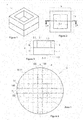
- figs 1 - 3 there is described as an example a piece P that has been produced using the method of the invention of material that in this example is glass.
- Fig 1 presents it in 3D, fig 2 directly from above and fig 3 cut A-A in the place indicated in fig 2 .
- the piece P is rectangular and its outside dimensions are x, y and z. Its cross section is in level x- y- direction square and it has been formed in the glass piece from its other x- y- surface a hollow reaching inside the piece, i.e. room 3.
- an optical component is put into this room and it is possible to focus visible light to this component through certain part of the glass piece.
- this part is wall 1, the first surface 1.1 and the second surface 1.2 of which are optically bright and plane.
- a rim 2 that goes around it and thus inside the outside dimensions x, y, z the before mentioned room 3 is formed reaching to the first surface 1.1 and the inside surface 2.1 of the rim.
- the thickness of the wall 1 is in this case a and the height of the rim is b.
- the before described piece P has been produced by an application of the method according to the invention as follows: According to the figs 4 - 6 two glass sheets, that is the first sheet 10 and the second sheet 11, have been placed upon each other upon a working underlay so that they have a common border surface 12.
- the mentioned sheets are plane, optically bright and they will be welded together using a laser beam 13a that has been focused to the level of the border surface 12. It can be seen in the fig 4 that the mentioned sheets will be joined with welds 14 that reach essentially from one edge to other of the sheet pair each other crossing linear welds.
- welds 14 that reach essentially from one edge to other of the sheet pair each other crossing linear welds.
- the combination C formed of the sheets 10, 11 there have been marked the lines to show the crossing points 100 where the combination is cut into pieces in the last phase of the method according to the invention.
- the distance between the cutting lines in two perpendicular directions corresponds to the dimensions x, y of the before mentioned piece P.
- the before mentioned welds 14 are formed on both sides of the mentioned crossing points near them so that the welds 14 form numerous square shape arc welds 14'.
- the sides of these arc welds are in certain such distance a from the crossing points 100 that it is possible to cut loose from the combination C glass pieces, that is pieces P using some known technique method along these cutting points without causing damage to the arc welds 14'.
- economical values for the distance a can be 25- 100 ⁇ m. However, this is not presented as a limitation for the usage of the invention but the value in question can always be selected case by case also outside this area.
- the arc weld 14' can be made gas tight or in some cases it can be made for instance using hemlock weld and the issues of the usage of the piece P determine case by case the requirements for the welding.
- a circular ablation is made inside each arc weld 14', more precisely inside the projection line in the thickness direction w of the sheets 10, 11 of this arc weld.
- the ablation is made using laser beam 13b so that it starts from the first surface 10.1 of the first sheet 10 and it is continued going round the ring through this sheet to its second surface 10.2 and as a result of this ablation a chink 15 is formed inside the arc weld 14' through the first sheet 10 and inside it a loose part 16 from the first sheet.
- an essentially part 16 size room 3 is formed in the combination C.
- the bottom of this room 3 is optically bright and plane part of the first surface 11.1 of the second plane 11.
- the oblation can be done in some other way than before for the second sheet 11, when the first sheet 10 needs to be optically bright. So the optical brightness is required for at least of the sheet whereof the coming transparent piece walls 1 are formed.
- the method according to the invention is not limited to removing the part 6 and to forming the room 3 only in the way that has been described above using the ablation.
- making the circular chink 15 can also be reached by other ways, like for example mechanically cutting or some other kind of laser technique. It is essential for the invention that by making the chink 15 as described and removing from inside it the part 16 an optically bright and plane wall 1 first surface 1.1 is obtained.
- the dimension z can be for instance 50 ⁇ m- 2 mm.
- the outside diameters for the sheets 10, 11 are in this example case about 150 mm.
- the method according to the invention can be use very widely in connection of different size and thickness sheets. In the market, there are as standard products for instance sheets of the diameter of 2" - 10" and their thicknesses vary in the before mentioned range 50 ⁇ m- 2 mm.
- the usage of the invention is however not limited only to the production of the pieces P of the presented size but it can be applied widely for different size products.
- the usage of the invention is not limited to the certain size standard preforms but it can be used much more widely.
- the focused laser beam 13b that causes the ablation about which the name "picoseconds-laser” is used can have the pulse length of for instance 10 picoseconds and the power can be tens of watts (W) when its advancing speed is a number of meters per second.
- the laser beam and the ablation advance going round certain circle and moving deeper with certain movement per round of the material when material disappears or is removed from this spot and a chink 15 is formed in the spot in question.
- the ablation or other work methods that are used in the method according to the invention do not harm the first surface 1.1 of the wall 1.
Landscapes
- Engineering & Computer Science (AREA)
- Physics & Mathematics (AREA)
- Optics & Photonics (AREA)
- Plasma & Fusion (AREA)
- Mechanical Engineering (AREA)
- Chemical & Material Sciences (AREA)
- Organic Chemistry (AREA)
- Microelectronics & Electronic Packaging (AREA)
- Materials Engineering (AREA)
- Chemical Kinetics & Catalysis (AREA)
- Signal Processing (AREA)
- General Chemical & Material Sciences (AREA)
- Oil, Petroleum & Natural Gas (AREA)
- Multimedia (AREA)
- Condensed Matter Physics & Semiconductors (AREA)
- Electromagnetism (AREA)
- General Physics & Mathematics (AREA)
- Computer Hardware Design (AREA)
- Power Engineering (AREA)
- Joining Of Glass To Other Materials (AREA)
- Optical Measuring Cells (AREA)
- Laser Beam Processing (AREA)
Abstract
Description
- The object of this invention is a method to produce a transparent piece to be used to protect an optical component which piece consists of at least one flat wall that is optically bright and a rim going round a certain surface of this wall and so a room is formed inside the dimensions of the piece limiting to a certain surface and the inside of the rim.
- The usages of the invention are in the production of the pieces used for the protection and the encapsuling of the optical components. These pieces are transparent for the visible light and made of glass, silicon and sapphire or combinations of them. It is typical for these pieces that the surfaces of certain wall are optically bright so that the light penetrates through them efficiently and without reflecting this light unfavorably. As an example of the optical components it can be mentioned CMOS sensors and different components of projectors.
- The before mentioned pieces are produced with the known technology so that first a for example rectangular piece of total height of the product is formed and then beginning from one of its sides a room is etched for the optical components to be used in connection of it and thus around of this room remains a part that is rim surrounding this component and in one side a wall that is transparent for the light that is entering and leaving the optical component.
- Another way to produce a piece of the object of the invention according to the known technology is to compose it of two parts. The first part is then a bright plate of glass, silicon or sapphire and the second part is a plate of glass, silicon or sapphire where there has been made an opening of suitable size for the optical component. These plates are placed upon each other, heated to the temperature of 400 - 1000 ºC and pressed together. They stick to each other because of the temperature and pressing power and thus form a piece of desired shape.
- The known technology that has been described above is used in the marked very widely when producing glass, silicon or sapphire contents pieces to be used in connection of the optical components.
- The greatest drawback of the known technique can be seen that when using it it is very laborious and expensive and many times even impossible to achieve a desired level quality product. In this case, the quality means optically bright surfaces and flat surface that let the light penetrate sufficiently without problems. Brightness of the surface is of course a relative concept but in this context can sufficiently brightness of the surface be seen the brightness of the glass, silicon and sapphire that is reached in the ordinary industrial production of glass, silicon and sapphire.
- When using an etching method, the bottom (for instance the so called inside surface) of the room to be etched gets the shape of cone, in which case the light penetrating through the wall is not reflected without disturbance. It is also very challenging to achieve a sufficient surface brightness when using the etching method and it is then necessary to make compromises between the production costs and the surface brightness.
- Another drawback of the known production method, that is pressing heated parts together is, that the heating causes heat tensions in the plates that are used and they change uneven the wall of the object of the penetration of the light so that there comes disturbance in the reflection of the light. Even though it is possible to achieve a sufficient surface brightness in this method this advantage is lost when the surfaces become none-plane.
- The meaning of this invention is to achieve such a method to produce transparent pieces to be used to protect optical components that avoids the drawbacks of the known technology. It is characteristic for the solution according to the invention that has been presented in the
claim 1 characterizing part. - The most important advantage of the invention can be seen to be that the production of the glass, silicon and sapphire or combination of these materials pieces that are to be made in accordance with it the wall that is meant to let the light to penetrate through surfaces are optically bright and plane so that the light beams penetrating through it reflect as anticipated and without disturbance.
- In this document the term "line welding" means all the welding that advances on a certain level, where no arc welding is formed by one welding. The term "transparent piece" means a piece that contains a transparent wall.
- The invention is described in more detail in the enclosed drawings, where
-
figs 1 - 3 present one transparent piece to be used to protect an optical component, -
fig 4 describes a setting where more than one before mentioned pieces are produced at a time using the method of the invention, -
fig 5 presents a cut detail drawing infig 4 where the place "Area 1" is described, -
fig 6 presents a sectional cut of the place "A-A". - Next, one for the invention favorable application is described referring to the before mentioned drawings.
- In
figs 1 - 3 there is described as an example a piece P that has been produced using the method of the invention of material that in this example is glass.Fig 1 presents it in 3D,fig 2 directly from above andfig 3 cut A-A in the place indicated infig 2 . The piece P is rectangular and its outside dimensions are x, y and z. Its cross section is in level x- y- direction square and it has been formed in the glass piece from its other x- y- surface a hollow reaching inside the piece, i.e.room 3. When using the piece P an optical component is put into this room and it is possible to focus visible light to this component through certain part of the glass piece. In the piece P of this example this part iswall 1, the first surface 1.1 and the second surface 1.2 of which are optically bright and plane. Around the first surface 1.1 there is arim 2 that goes around it and thus inside the outside dimensions x, y, z the before mentionedroom 3 is formed reaching to the first surface 1.1 and the inside surface 2.1 of the rim. The thickness of thewall 1 is in this case a and the height of the rim is b. The piece P is fastened to the usage object to its rim's 1 opposite surface. - The before described piece P has been produced by an application of the method according to the invention as follows: According to the
figs 4 - 6 two glass sheets, that is thefirst sheet 10 and thesecond sheet 11, have been placed upon each other upon a working underlay so that they have acommon border surface 12. The mentioned sheets are plane, optically bright and they will be welded together using alaser beam 13a that has been focused to the level of theborder surface 12. It can be seen in thefig 4 that the mentioned sheets will be joined withwelds 14 that reach essentially from one edge to other of the sheet pair each other crossing linear welds. In the combination C formed of thesheets crossing points 100 where the combination is cut into pieces in the last phase of the method according to the invention. The distance between the cutting lines in two perpendicular directions corresponds to the dimensions x, y of the before mentioned piece P. The before mentionedwelds 14 are formed on both sides of the mentioned crossing points near them so that thewelds 14 form numerous square shape arc welds 14'. The sides of these arc welds are in certain such distance a from thecrossing points 100 that it is possible to cut loose from the combination C glass pieces, that is pieces P using some known technique method along these cutting points without causing damage to the arc welds 14'. It can be mentioned that economical values for the distance a can be 25- 100 µm. However, this is not presented as a limitation for the usage of the invention but the value in question can always be selected case by case also outside this area. The arc weld 14' can be made gas tight or in some cases it can be made for instance using hemlock weld and the issues of the usage of the piece P determine case by case the requirements for the welding. - In this example, in the next stage of the method a circular ablation is made inside each arc weld 14', more precisely inside the projection line in the thickness direction w of the
sheets laser beam 13b so that it starts from the first surface 10.1 of thefirst sheet 10 and it is continued going round the ring through this sheet to its second surface 10.2 and as a result of this ablation achink 15 is formed inside the arc weld 14' through thefirst sheet 10 and inside it aloose part 16 from the first sheet. When thispart 16 is taken away, an essentiallypart 16size room 3 is formed in the combination C. The bottom of thisroom 3 is optically bright and plane part of the first surface 11.1 of thesecond plane 11. When a cutting is performed for the preform along the cutting points 100 a certain amount of pieces P get loose where everyone has awall 1 and arim 2. - Naturally, the oblation can be done in some other way than before for the
second sheet 11, when thefirst sheet 10 needs to be optically bright. So the optical brightness is required for at least of the sheet whereof the comingtransparent piece walls 1 are formed. - It is possible to produce, using the method of the invention, transparent pieces P where the raw material is glass, silicon or sapphire of that are composed of more than one of these materials.
- The method according to the invention is not limited to removing the part 6 and to forming the
room 3 only in the way that has been described above using the ablation. To get loose thispart 16 making thecircular chink 15 can also be reached by other ways, like for example mechanically cutting or some other kind of laser technique. It is essential for the invention that by making thechink 15 as described and removing from inside it thepart 16 an optically bright andplane wall 1 first surface 1.1 is obtained. - In the example case that has been presented before the dimensions of the piece P are: x and
y 15 mm and the dimension z can be for instance 50 µm- 2 mm. With the given values of x and y the outside diameters for thesheets second sheet - It is essential for the method according to the invention that the surface brightness and the plainness of a factory produced sheets are exploited to obtain a piece P that is optically bright and the
wall 1 with good reflection capabilities. This can be reached using the invention so that neither surface off thewall 1 is machined nor in the production of the piece P used preforms are caused shape changing heat stress. It is known that laser ablation does no cause note worthy increase in the temperature. The same applies to the mechanical working because the temperature can be controlled by for instance cooling. - It is possible to produce different shape pieces P with the method according to the invention. In addition to rectangular pieces it is possible to make for instance polygons, cylinders, otherwise curvilinear and combinations of these shape pieces. It is essential for those shapes that they can be made uniting two sheets. The inside 2.1 of the
rim 2 of the piece P can be made according to the invention method also in many shapes. All the presented methods are possible and the factor that determines the shape of theroom 3 can naturally be for instance the shape of the optical device that is to be placed there. - When the ablation is used its advancing speed can be adapted case by case. The
focused laser beam 13b that causes the ablation about which the name "picoseconds-laser" is used can have the pulse length of forinstance 10 picoseconds and the power can be tens of watts (W) when its advancing speed is a number of meters per second. The laser beam and the ablation advance going round certain circle and moving deeper with certain movement per round of the material when material disappears or is removed from this spot and achink 15 is formed in the spot in question. The ablation or other work methods that are used in the method according to the invention do not harm the first surface 1.1 of thewall 1. - It is worth noticing that even though in this description it has been kept to one for invention favorable realization example this does not however mean that the usage of the invention would be limited only to this type of example but many variations are possible within the inventive idea of the claims.
Claims (7)
- A method to produce a transparent piece (P) to be used to protect an optical component which piece consists of at least one plane wall (1) that is optically bright and a rim (2) going round the surface (1.1) of this wall when inside the out dimensions (x, y, z) a room (3) is formed limiting to the mentioned first surface (1.1) and the inside surface (2.1) of the rim and which method is characterized thereof that using it one or more pieces (P) are produced as follows:a. the first sheet (10) and the second sheet (11) where at least the one that is used to form wall/walls (1) is optically bright, are placed against each other,b.the surfaces (10.2, 11.1) of the mentioned sheet that are against each other are welded together using a focused laser beam (13a) at the level of their common junction plane (12),c. In welding the before mentioned, an arc weld (14') is formed either with a continuous weld or crossing welds (14) for each piece (P) to be produced,d.Inside the thickness wise (w) projection line of each arc weld (14') of the mentioned sheets (10, 11) a machining is performed to form an arc like chink (15) that reaches from the mentioned sheets (10, 11) through that sheet that is used to form the rim / rims of the piece / -s (P).e. the chink (15) that has been formed in each mentioned machining place loosens essentially room (3) size part (16) from the sheet that is being machined,f. Part / parts (16) are taken away from the mentioned sheet when a piece (P) is formed or a preform that includes a number of pieces (P) that are stuck to each other,g. in case of preforms, the pieces (P) are cut loose from it along the welding points (100) that are situated between the arc welds (14') of these pieces.
- The method according to the claim 1 characterized thereof that the raw material of the transparent piece (P) is glass, silicon or sapphire or combination of glass-silicon/sapphire, glass-silicon, glass-sapphire, or silicon-sapphire.
- The method according to the claim 1 or 2 characterized thereof that the machining of the chink (15) belonging to it is performed by ablation with a focused laser beam (13b), with mechanical work or by laser technique other than ablation.
- The method according to some of the claims 1 - 3 characterized thereof that the piece (P) produced by it is rectangular, polygon or cylinder.
- The method according to some of the claims 1 - 4 characterized thereof that the room (3) of the piece made by it is rectangular, polygon or cylinder.
- The method according to some of the claims 1 - 5 characterized thereof that the arc weld (14') is made gas tight.
- The method according to some of the claims 1 - 6 characterized thereof that the first and the second sheets (10, 11) that are used there are factory fabricated sheets.
Applications Claiming Priority (1)
| Application Number | Priority Date | Filing Date | Title |
|---|---|---|---|
| FI20140257A FI125935B (en) | 2014-09-26 | 2014-09-26 | A method of manufacturing a transparent body for protection of an optical component |
Publications (3)
| Publication Number | Publication Date |
|---|---|
| EP3012059A2 true EP3012059A2 (en) | 2016-04-27 |
| EP3012059A3 EP3012059A3 (en) | 2016-06-01 |
| EP3012059B1 EP3012059B1 (en) | 2017-10-18 |
Family
ID=54207346
Family Applications (1)
| Application Number | Title | Priority Date | Filing Date |
|---|---|---|---|
| EP15186879.1A Active EP3012059B1 (en) | 2014-09-26 | 2015-09-25 | Method to produce a transparent piece to be used to protect an optical component |
Country Status (2)
| Country | Link |
|---|---|
| EP (1) | EP3012059B1 (en) |
| FI (1) | FI125935B (en) |
Cited By (5)
| Publication number | Priority date | Publication date | Assignee | Title |
|---|---|---|---|---|
| CN109987567A (en) * | 2017-12-20 | 2019-07-09 | 罗伯特·博世有限公司 | Laser bonding method and micromechanical devices with laser bonding interconnecting piece |
| EP3812352A1 (en) | 2019-10-24 | 2021-04-28 | Schott Primoceler Oy | Glass compound arrangement |
| JP2021088468A (en) * | 2019-12-02 | 2021-06-10 | 日本電気硝子株式会社 | Laminated substrate and method for producing the same |
| US11975962B2 (en) | 2019-07-24 | 2024-05-07 | Schott Ag | Hermetically sealed transparent cavity and package for same |
| US11993511B2 (en) | 2019-07-16 | 2024-05-28 | Schott Ag | Hermetically sealed, toughened glass package and method for producing same |
Families Citing this family (16)
| Publication number | Priority date | Publication date | Assignee | Title |
|---|---|---|---|---|
| DE102019121298A1 (en) | 2019-08-07 | 2021-02-11 | Schott Ag | Hermetically sealed glass casing |
| DE102019125963A1 (en) | 2019-09-26 | 2021-04-01 | Schott Ag | Hermetically sealed glass casing |
| DE202020005535U1 (en) | 2020-01-15 | 2021-10-14 | Schott Ag | Hermetically sealed, transparent cavity and its housing |
| DE102020100819A1 (en) | 2020-01-15 | 2021-07-15 | Schott Ag | Hermetically sealed, transparent cavity and its housing |
| DE102020104613A1 (en) | 2020-02-21 | 2021-08-26 | Schott Ag | Hermetically sealed glass casing |
| DE102020117194B4 (en) | 2020-06-30 | 2023-06-22 | Schott Ag | Hermetically sealed enclosure and method of making same |
| DE102020129220A1 (en) | 2020-11-05 | 2022-05-05 | Schott Ag | Bond Quality Index |
| EP4241301A2 (en) | 2020-11-08 | 2023-09-13 | Schott Ag | Hermetically connected arrangement, enclosure and method for the production thereof |
| DE102020129380A1 (en) | 2020-11-08 | 2022-05-12 | Schott Ag | Hermetically bonded assembly |
| EP4166497A1 (en) | 2021-10-15 | 2023-04-19 | Schott Ag | Enclosure with information pattern |
| EP4177935A1 (en) | 2021-11-03 | 2023-05-10 | Schott Ag | Hermetic laser-welded enclosure |
| DE102021129411A1 (en) | 2021-11-11 | 2023-05-11 | Schott Ag | Hermetically bonded assembly |
| DE102022116612A1 (en) | 2022-07-04 | 2024-01-04 | Schott Ag | Hermetically sealed enclosure and method of designing the weld joint for such an enclosure |
| EP4344619A1 (en) | 2022-09-29 | 2024-04-03 | Schott Ag | Laser welded enclosure for electronics, circuitry or sensors |
| EP4393869A1 (en) * | 2022-12-28 | 2024-07-03 | Schott Ag | Method for welding substrates and welded substrates |
| EP4424651A1 (en) | 2023-03-02 | 2024-09-04 | Schott Ag | Bonded substrate arrangement and method for manufacturing of such an arrangement |
Family Cites Families (3)
| Publication number | Priority date | Publication date | Assignee | Title |
|---|---|---|---|---|
| EP2075082B1 (en) * | 2006-09-22 | 2015-11-11 | NEC SCHOTT Components Corporation | Substance joining method |
| JP5481167B2 (en) * | 2009-11-12 | 2014-04-23 | 浜松ホトニクス株式会社 | Glass welding method |
| DE102010038554A1 (en) * | 2010-07-28 | 2012-02-02 | Osram Ag | Optoelectronic semiconductor component and associated manufacturing method |
-
2014
- 2014-09-26 FI FI20140257A patent/FI125935B/en active IP Right Grant
-
2015
- 2015-09-25 EP EP15186879.1A patent/EP3012059B1/en active Active
Non-Patent Citations (1)
| Title |
|---|
| None |
Cited By (5)
| Publication number | Priority date | Publication date | Assignee | Title |
|---|---|---|---|---|
| CN109987567A (en) * | 2017-12-20 | 2019-07-09 | 罗伯特·博世有限公司 | Laser bonding method and micromechanical devices with laser bonding interconnecting piece |
| US11993511B2 (en) | 2019-07-16 | 2024-05-28 | Schott Ag | Hermetically sealed, toughened glass package and method for producing same |
| US11975962B2 (en) | 2019-07-24 | 2024-05-07 | Schott Ag | Hermetically sealed transparent cavity and package for same |
| EP3812352A1 (en) | 2019-10-24 | 2021-04-28 | Schott Primoceler Oy | Glass compound arrangement |
| JP2021088468A (en) * | 2019-12-02 | 2021-06-10 | 日本電気硝子株式会社 | Laminated substrate and method for producing the same |
Also Published As
| Publication number | Publication date |
|---|---|
| FI20140257A (en) | 2016-03-27 |
| EP3012059A3 (en) | 2016-06-01 |
| EP3012059B1 (en) | 2017-10-18 |
| FI125935B (en) | 2016-04-15 |
Similar Documents
| Publication | Publication Date | Title |
|---|---|---|
| EP3012059A2 (en) | Method to produce a transparent piece to be used to protect an optical component | |
| US10392290B2 (en) | Processing 3D shaped transparent brittle substrate | |
| JP6588911B2 (en) | 3D formation of glass | |
| Žemaitis et al. | Rapid high-quality 3D micro-machining by optimised efficient ultrashort laser ablation | |
| JP6768781B2 (en) | Method and device for separating a piece from a planar glass member by laser assist | |
| TWI677394B (en) | Method of closed form release for brittle materials using burst ultrafast laser pulses | |
| JP7150613B2 (en) | Method for joining substrates and components using substrate structuring | |
| KR102292611B1 (en) | Method of Laser Cutting a Sapphire Substrate by Lasers and an Article Comprising Sapphire with Edge Having a Series of Defects | |
| TWI632975B (en) | Methods for laser drilling materials and glass articles | |
| JP6629207B2 (en) | Edge chamfering method | |
| JP5525601B2 (en) | Substrate processing method using laser | |
| TWI517922B (en) | Methods for cutting a fragile material | |
| EP3356300A1 (en) | Method and device for laser processing of transparent materials | |
| CN106891096A (en) | A kind of laser cutting device and cutting method | |
| JP2017528323A (en) | Interface blocks, systems and methods for cutting substrates that transmit within a wavelength range using such interface blocks | |
| WO2015104762A1 (en) | Laser welding method | |
| CN104884205A (en) | Methods of forming images by laser micromachining | |
| US10710922B2 (en) | Methods and apparatus for cutting a substrate | |
| KR20170082649A (en) | Precision laser scoring | |
| JP2009082958A (en) | Laser beam machining apparatus and axicon lens | |
| KR20160093593A (en) | Method and apparatus for internally marking a substrate having a rough surface | |
| EP2962804A3 (en) | Method of welding two substrate pieces together using a focused laser beam | |
| Ascari et al. | Nanosecond pulsed laser welding of high carbon steels | |
| JP2024075582A (en) | Method for introducing recess into substrate | |
| GB2583090A (en) | Method for joining a first substrate to a second substrate |
Legal Events
| Date | Code | Title | Description |
|---|---|---|---|
| PUAI | Public reference made under article 153(3) epc to a published international application that has entered the european phase |
Free format text: ORIGINAL CODE: 0009012 |
|
| AK | Designated contracting states |
Kind code of ref document: A2 Designated state(s): AL AT BE BG CH CY CZ DE DK EE ES FI FR GB GR HR HU IE IS IT LI LT LU LV MC MK MT NL NO PL PT RO RS SE SI SK SM TR |
|
| AX | Request for extension of the european patent |
Extension state: BA ME |
|
| PUAL | Search report despatched |
Free format text: ORIGINAL CODE: 0009013 |
|
| AK | Designated contracting states |
Kind code of ref document: A3 Designated state(s): AL AT BE BG CH CY CZ DE DK EE ES FI FR GB GR HR HU IE IS IT LI LT LU LV MC MK MT NL NO PL PT RO RS SE SI SK SM TR |
|
| AX | Request for extension of the european patent |
Extension state: BA ME |
|
| RIC1 | Information provided on ipc code assigned before grant |
Ipc: B23K 26/38 20140101ALI20160426BHEP Ipc: B23K 26/362 20140101ALI20160426BHEP Ipc: C03B 23/203 20060101ALI20160426BHEP Ipc: B23K 26/324 20140101ALI20160426BHEP Ipc: B23K 26/26 20140101ALI20160426BHEP Ipc: B23K 26/20 20140101ALI20160426BHEP Ipc: B23K 26/244 20140101ALI20160426BHEP Ipc: B23K 26/00 20140101AFI20160426BHEP |
|
| 17P | Request for examination filed |
Effective date: 20161117 |
|
| RBV | Designated contracting states (corrected) |
Designated state(s): AL AT BE BG CH CY CZ DE DK EE ES FI FR GB GR HR HU IE IS IT LI LT LU LV MC MK MT NL NO PL PT RO RS SE SI SK SM TR |
|
| GRAP | Despatch of communication of intention to grant a patent |
Free format text: ORIGINAL CODE: EPIDOSNIGR1 |
|
| INTG | Intention to grant announced |
Effective date: 20170130 |
|
| GRAS | Grant fee paid |
Free format text: ORIGINAL CODE: EPIDOSNIGR3 |
|
| GRAJ | Information related to disapproval of communication of intention to grant by the applicant or resumption of examination proceedings by the epo deleted |
Free format text: ORIGINAL CODE: EPIDOSDIGR1 |
|
| GRAL | Information related to payment of fee for publishing/printing deleted |
Free format text: ORIGINAL CODE: EPIDOSDIGR3 |
|
| INTC | Intention to grant announced (deleted) | ||
| GRAP | Despatch of communication of intention to grant a patent |
Free format text: ORIGINAL CODE: EPIDOSNIGR1 |
|
| INTG | Intention to grant announced |
Effective date: 20170807 |
|
| GRAA | (expected) grant |
Free format text: ORIGINAL CODE: 0009210 |
|
| AK | Designated contracting states |
Kind code of ref document: B1 Designated state(s): AL AT BE BG CH CY CZ DE DK EE ES FI FR GB GR HR HU IE IS IT LI LT LU LV MC MK MT NL NO PL PT RO RS SE SI SK SM TR |
|
| RAP1 | Party data changed (applicant data changed or rights of an application transferred) |
Owner name: PRIMOCELER OY |
|
| REG | Reference to a national code |
Ref country code: GB Ref legal event code: FG4D |
|
| RIN1 | Information on inventor provided before grant (corrected) |
Inventor name: MAEAETTAENEN, ANTTI |
|
| REG | Reference to a national code |
Ref country code: CH Ref legal event code: EP |
|
| REG | Reference to a national code |
Ref country code: AT Ref legal event code: REF Ref document number: 937516 Country of ref document: AT Kind code of ref document: T Effective date: 20171115 Ref country code: IE Ref legal event code: FG4D |
|
| REG | Reference to a national code |
Ref country code: DE Ref legal event code: R096 Ref document number: 602015005407 Country of ref document: DE |
|
| REG | Reference to a national code |
Ref country code: CH Ref legal event code: NV Representative=s name: OFFICE ERNEST T. FREYLINGER S.A., CH |
|
| REG | Reference to a national code |
Ref country code: NL Ref legal event code: MP Effective date: 20171018 |
|
| REG | Reference to a national code |
Ref country code: DE Ref legal event code: R082 Ref document number: 602015005407 Country of ref document: DE Representative=s name: OFFICE FREYLINGER S.A., LU |
|
| REG | Reference to a national code |
Ref country code: LT Ref legal event code: MG4D |
|
| REG | Reference to a national code |
Ref country code: AT Ref legal event code: MK05 Ref document number: 937516 Country of ref document: AT Kind code of ref document: T Effective date: 20171018 |
|
| PG25 | Lapsed in a contracting state [announced via postgrant information from national office to epo] |
Ref country code: NL Free format text: LAPSE BECAUSE OF FAILURE TO SUBMIT A TRANSLATION OF THE DESCRIPTION OR TO PAY THE FEE WITHIN THE PRESCRIBED TIME-LIMIT Effective date: 20171018 |
|
| PG25 | Lapsed in a contracting state [announced via postgrant information from national office to epo] |
Ref country code: SE Free format text: LAPSE BECAUSE OF FAILURE TO SUBMIT A TRANSLATION OF THE DESCRIPTION OR TO PAY THE FEE WITHIN THE PRESCRIBED TIME-LIMIT Effective date: 20171018 Ref country code: ES Free format text: LAPSE BECAUSE OF FAILURE TO SUBMIT A TRANSLATION OF THE DESCRIPTION OR TO PAY THE FEE WITHIN THE PRESCRIBED TIME-LIMIT Effective date: 20171018 Ref country code: FI Free format text: LAPSE BECAUSE OF FAILURE TO SUBMIT A TRANSLATION OF THE DESCRIPTION OR TO PAY THE FEE WITHIN THE PRESCRIBED TIME-LIMIT Effective date: 20171018 Ref country code: LT Free format text: LAPSE BECAUSE OF FAILURE TO SUBMIT A TRANSLATION OF THE DESCRIPTION OR TO PAY THE FEE WITHIN THE PRESCRIBED TIME-LIMIT Effective date: 20171018 Ref country code: NO Free format text: LAPSE BECAUSE OF FAILURE TO SUBMIT A TRANSLATION OF THE DESCRIPTION OR TO PAY THE FEE WITHIN THE PRESCRIBED TIME-LIMIT Effective date: 20180118 |
|
| PG25 | Lapsed in a contracting state [announced via postgrant information from national office to epo] |
Ref country code: LV Free format text: LAPSE BECAUSE OF FAILURE TO SUBMIT A TRANSLATION OF THE DESCRIPTION OR TO PAY THE FEE WITHIN THE PRESCRIBED TIME-LIMIT Effective date: 20171018 Ref country code: IS Free format text: LAPSE BECAUSE OF FAILURE TO SUBMIT A TRANSLATION OF THE DESCRIPTION OR TO PAY THE FEE WITHIN THE PRESCRIBED TIME-LIMIT Effective date: 20180218 Ref country code: AT Free format text: LAPSE BECAUSE OF FAILURE TO SUBMIT A TRANSLATION OF THE DESCRIPTION OR TO PAY THE FEE WITHIN THE PRESCRIBED TIME-LIMIT Effective date: 20171018 Ref country code: RS Free format text: LAPSE BECAUSE OF FAILURE TO SUBMIT A TRANSLATION OF THE DESCRIPTION OR TO PAY THE FEE WITHIN THE PRESCRIBED TIME-LIMIT Effective date: 20171018 Ref country code: HR Free format text: LAPSE BECAUSE OF FAILURE TO SUBMIT A TRANSLATION OF THE DESCRIPTION OR TO PAY THE FEE WITHIN THE PRESCRIBED TIME-LIMIT Effective date: 20171018 Ref country code: BG Free format text: LAPSE BECAUSE OF FAILURE TO SUBMIT A TRANSLATION OF THE DESCRIPTION OR TO PAY THE FEE WITHIN THE PRESCRIBED TIME-LIMIT Effective date: 20180118 Ref country code: GR Free format text: LAPSE BECAUSE OF FAILURE TO SUBMIT A TRANSLATION OF THE DESCRIPTION OR TO PAY THE FEE WITHIN THE PRESCRIBED TIME-LIMIT Effective date: 20180119 |
|
| REG | Reference to a national code |
Ref country code: DE Ref legal event code: R097 Ref document number: 602015005407 Country of ref document: DE |
|
| PG25 | Lapsed in a contracting state [announced via postgrant information from national office to epo] |
Ref country code: SK Free format text: LAPSE BECAUSE OF FAILURE TO SUBMIT A TRANSLATION OF THE DESCRIPTION OR TO PAY THE FEE WITHIN THE PRESCRIBED TIME-LIMIT Effective date: 20171018 Ref country code: CZ Free format text: LAPSE BECAUSE OF FAILURE TO SUBMIT A TRANSLATION OF THE DESCRIPTION OR TO PAY THE FEE WITHIN THE PRESCRIBED TIME-LIMIT Effective date: 20171018 Ref country code: DK Free format text: LAPSE BECAUSE OF FAILURE TO SUBMIT A TRANSLATION OF THE DESCRIPTION OR TO PAY THE FEE WITHIN THE PRESCRIBED TIME-LIMIT Effective date: 20171018 Ref country code: EE Free format text: LAPSE BECAUSE OF FAILURE TO SUBMIT A TRANSLATION OF THE DESCRIPTION OR TO PAY THE FEE WITHIN THE PRESCRIBED TIME-LIMIT Effective date: 20171018 |
|
| PLBE | No opposition filed within time limit |
Free format text: ORIGINAL CODE: 0009261 |
|
| STAA | Information on the status of an ep patent application or granted ep patent |
Free format text: STATUS: NO OPPOSITION FILED WITHIN TIME LIMIT |
|
| PG25 | Lapsed in a contracting state [announced via postgrant information from national office to epo] |
Ref country code: PL Free format text: LAPSE BECAUSE OF FAILURE TO SUBMIT A TRANSLATION OF THE DESCRIPTION OR TO PAY THE FEE WITHIN THE PRESCRIBED TIME-LIMIT Effective date: 20171018 Ref country code: IT Free format text: LAPSE BECAUSE OF FAILURE TO SUBMIT A TRANSLATION OF THE DESCRIPTION OR TO PAY THE FEE WITHIN THE PRESCRIBED TIME-LIMIT Effective date: 20171018 Ref country code: RO Free format text: LAPSE BECAUSE OF FAILURE TO SUBMIT A TRANSLATION OF THE DESCRIPTION OR TO PAY THE FEE WITHIN THE PRESCRIBED TIME-LIMIT Effective date: 20171018 Ref country code: SM Free format text: LAPSE BECAUSE OF FAILURE TO SUBMIT A TRANSLATION OF THE DESCRIPTION OR TO PAY THE FEE WITHIN THE PRESCRIBED TIME-LIMIT Effective date: 20171018 |
|
| REG | Reference to a national code |
Ref country code: FR Ref legal event code: PLFP Year of fee payment: 4 |
|
| 26N | No opposition filed |
Effective date: 20180719 |
|
| PG25 | Lapsed in a contracting state [announced via postgrant information from national office to epo] |
Ref country code: SI Free format text: LAPSE BECAUSE OF FAILURE TO SUBMIT A TRANSLATION OF THE DESCRIPTION OR TO PAY THE FEE WITHIN THE PRESCRIBED TIME-LIMIT Effective date: 20171018 |
|
| PG25 | Lapsed in a contracting state [announced via postgrant information from national office to epo] |
Ref country code: MC Free format text: LAPSE BECAUSE OF FAILURE TO SUBMIT A TRANSLATION OF THE DESCRIPTION OR TO PAY THE FEE WITHIN THE PRESCRIBED TIME-LIMIT Effective date: 20171018 |
|
| REG | Reference to a national code |
Ref country code: BE Ref legal event code: MM Effective date: 20180930 |
|
| REG | Reference to a national code |
Ref country code: IE Ref legal event code: MM4A |
|
| PG25 | Lapsed in a contracting state [announced via postgrant information from national office to epo] |
Ref country code: LU Free format text: LAPSE BECAUSE OF NON-PAYMENT OF DUE FEES Effective date: 20180925 |
|
| PG25 | Lapsed in a contracting state [announced via postgrant information from national office to epo] |
Ref country code: IE Free format text: LAPSE BECAUSE OF NON-PAYMENT OF DUE FEES Effective date: 20180925 |
|
| PG25 | Lapsed in a contracting state [announced via postgrant information from national office to epo] |
Ref country code: BE Free format text: LAPSE BECAUSE OF NON-PAYMENT OF DUE FEES Effective date: 20180930 |
|
| PG25 | Lapsed in a contracting state [announced via postgrant information from national office to epo] |
Ref country code: MT Free format text: LAPSE BECAUSE OF NON-PAYMENT OF DUE FEES Effective date: 20180925 |
|
| PG25 | Lapsed in a contracting state [announced via postgrant information from national office to epo] |
Ref country code: TR Free format text: LAPSE BECAUSE OF FAILURE TO SUBMIT A TRANSLATION OF THE DESCRIPTION OR TO PAY THE FEE WITHIN THE PRESCRIBED TIME-LIMIT Effective date: 20171018 |
|
| PG25 | Lapsed in a contracting state [announced via postgrant information from national office to epo] |
Ref country code: PT Free format text: LAPSE BECAUSE OF FAILURE TO SUBMIT A TRANSLATION OF THE DESCRIPTION OR TO PAY THE FEE WITHIN THE PRESCRIBED TIME-LIMIT Effective date: 20171018 |
|
| PG25 | Lapsed in a contracting state [announced via postgrant information from national office to epo] |
Ref country code: HU Free format text: LAPSE BECAUSE OF FAILURE TO SUBMIT A TRANSLATION OF THE DESCRIPTION OR TO PAY THE FEE WITHIN THE PRESCRIBED TIME-LIMIT; INVALID AB INITIO Effective date: 20150925 Ref country code: CY Free format text: LAPSE BECAUSE OF FAILURE TO SUBMIT A TRANSLATION OF THE DESCRIPTION OR TO PAY THE FEE WITHIN THE PRESCRIBED TIME-LIMIT Effective date: 20171018 Ref country code: MK Free format text: LAPSE BECAUSE OF NON-PAYMENT OF DUE FEES Effective date: 20171018 |
|
| PG25 | Lapsed in a contracting state [announced via postgrant information from national office to epo] |
Ref country code: AL Free format text: LAPSE BECAUSE OF FAILURE TO SUBMIT A TRANSLATION OF THE DESCRIPTION OR TO PAY THE FEE WITHIN THE PRESCRIBED TIME-LIMIT Effective date: 20171018 |
|
| REG | Reference to a national code |
Ref country code: DE Ref legal event code: R081 Ref document number: 602015005407 Country of ref document: DE Owner name: SCHOTT PRIMOCELER OY, FI Free format text: FORMER OWNER: PRIMOCELER OY, TAMPERE, FI |
|
| P01 | Opt-out of the competence of the unified patent court (upc) registered |
Effective date: 20230516 |
|
| PGFP | Annual fee paid to national office [announced via postgrant information from national office to epo] |
Ref country code: CH Payment date: 20231001 Year of fee payment: 9 |
|
| PGFP | Annual fee paid to national office [announced via postgrant information from national office to epo] |
Ref country code: DE Payment date: 20240919 Year of fee payment: 10 |
|
| PGFP | Annual fee paid to national office [announced via postgrant information from national office to epo] |
Ref country code: GB Payment date: 20240918 Year of fee payment: 10 |
|
| PGFP | Annual fee paid to national office [announced via postgrant information from national office to epo] |
Ref country code: FR Payment date: 20240916 Year of fee payment: 10 |