EP3010151A1 - Method and apparatus for a buck converter with pulse frequency modulation - Google Patents
Method and apparatus for a buck converter with pulse frequency modulation Download PDFInfo
- Publication number
- EP3010151A1 EP3010151A1 EP14188907.1A EP14188907A EP3010151A1 EP 3010151 A1 EP3010151 A1 EP 3010151A1 EP 14188907 A EP14188907 A EP 14188907A EP 3010151 A1 EP3010151 A1 EP 3010151A1
- Authority
- EP
- European Patent Office
- Prior art keywords
- time
- proportional
- vdd
- buck converter
- comparator
- Prior art date
- Legal status (The legal status is an assumption and is not a legal conclusion. Google has not performed a legal analysis and makes no representation as to the accuracy of the status listed.)
- Granted
Links
Images



Classifications
-
- H—ELECTRICITY
- H03—ELECTRONIC CIRCUITRY
- H03K—PULSE TECHNIQUE
- H03K7/00—Modulating pulses with a continuously-variable modulating signal
- H03K7/06—Frequency or rate modulation, i.e. PFM or PRM
-
- H—ELECTRICITY
- H02—GENERATION; CONVERSION OR DISTRIBUTION OF ELECTRIC POWER
- H02M—APPARATUS FOR CONVERSION BETWEEN AC AND AC, BETWEEN AC AND DC, OR BETWEEN DC AND DC, AND FOR USE WITH MAINS OR SIMILAR POWER SUPPLY SYSTEMS; CONVERSION OF DC OR AC INPUT POWER INTO SURGE OUTPUT POWER; CONTROL OR REGULATION THEREOF
- H02M3/00—Conversion of DC power input into DC power output
- H02M3/02—Conversion of DC power input into DC power output without intermediate conversion into AC
- H02M3/04—Conversion of DC power input into DC power output without intermediate conversion into AC by static converters
- H02M3/10—Conversion of DC power input into DC power output without intermediate conversion into AC by static converters using discharge tubes with control electrode or semiconductor devices with control electrode
- H02M3/145—Conversion of DC power input into DC power output without intermediate conversion into AC by static converters using discharge tubes with control electrode or semiconductor devices with control electrode using devices of a triode or transistor type requiring continuous application of a control signal
- H02M3/155—Conversion of DC power input into DC power output without intermediate conversion into AC by static converters using discharge tubes with control electrode or semiconductor devices with control electrode using devices of a triode or transistor type requiring continuous application of a control signal using semiconductor devices only
- H02M3/156—Conversion of DC power input into DC power output without intermediate conversion into AC by static converters using discharge tubes with control electrode or semiconductor devices with control electrode using devices of a triode or transistor type requiring continuous application of a control signal using semiconductor devices only with automatic control of output voltage or current, e.g. switching regulators
- H02M3/158—Conversion of DC power input into DC power output without intermediate conversion into AC by static converters using discharge tubes with control electrode or semiconductor devices with control electrode using devices of a triode or transistor type requiring continuous application of a control signal using semiconductor devices only with automatic control of output voltage or current, e.g. switching regulators including plural semiconductor devices as final control devices for a single load
- H02M3/1588—Conversion of DC power input into DC power output without intermediate conversion into AC by static converters using discharge tubes with control electrode or semiconductor devices with control electrode using devices of a triode or transistor type requiring continuous application of a control signal using semiconductor devices only with automatic control of output voltage or current, e.g. switching regulators including plural semiconductor devices as final control devices for a single load comprising at least one synchronous rectifier element
-
- H—ELECTRICITY
- H02—GENERATION; CONVERSION OR DISTRIBUTION OF ELECTRIC POWER
- H02M—APPARATUS FOR CONVERSION BETWEEN AC AND AC, BETWEEN AC AND DC, OR BETWEEN DC AND DC, AND FOR USE WITH MAINS OR SIMILAR POWER SUPPLY SYSTEMS; CONVERSION OF DC OR AC INPUT POWER INTO SURGE OUTPUT POWER; CONTROL OR REGULATION THEREOF
- H02M1/00—Details of apparatus for conversion
- H02M1/0003—Details of control, feedback or regulation circuits
- H02M1/0032—Control circuits allowing low power mode operation, e.g. in standby mode
-
- Y—GENERAL TAGGING OF NEW TECHNOLOGICAL DEVELOPMENTS; GENERAL TAGGING OF CROSS-SECTIONAL TECHNOLOGIES SPANNING OVER SEVERAL SECTIONS OF THE IPC; TECHNICAL SUBJECTS COVERED BY FORMER USPC CROSS-REFERENCE ART COLLECTIONS [XRACs] AND DIGESTS
- Y02—TECHNOLOGIES OR APPLICATIONS FOR MITIGATION OR ADAPTATION AGAINST CLIMATE CHANGE
- Y02B—CLIMATE CHANGE MITIGATION TECHNOLOGIES RELATED TO BUILDINGS, e.g. HOUSING, HOUSE APPLIANCES OR RELATED END-USER APPLICATIONS
- Y02B70/00—Technologies for an efficient end-user side electric power management and consumption
- Y02B70/10—Technologies improving the efficiency by using switched-mode power supplies [SMPS], i.e. efficient power electronics conversion e.g. power factor correction or reduction of losses in power supplies or efficient standby modes
Definitions
- the disclosure relates generally to power supply circuits and methods and, more particularly, to buck type converters, circuit and a method thereof.
- DC-DC converters are voltage regulators used in conjunction with semiconductor devices, integrated circuit (IC), battery chargers, and other applications.
- DC-DC converters can be used in digital, analog, and power applications to deliver a regulated supply voltage.
- FIG. 1 illustrates a typical implementation of a buck DC/DC output stage supplying a resistive load.
- the circuit comprises of a voltage source VDD 10, and output voltage VOUT 20, a p-channel MOSFET switch 30, a n-channel MOSFET switch 40.
- An inductor element 50 is electrically couples the switch network (p-channel MOSFET switch 30 and a n-channel MOSFET switch 40) and the output load (e.g. he output load consists of a d capacitor 60 and resistive load 70).
- a buck converter generates a pulse width modulation (PWM) switching voltage at the LX node, denoted as VLX.
- PWM pulse width modulation
- Buck converters operate in one of two modes, the pulse width modulation (PWM) mode, and the pulse frequency modulation (PFM) mode.
- PWM pulse width modulation
- PFM pulse frequency modulation
- the frequency of operation is fixed.
- the frequency is allowed to change with the load current.
- the p-channel MOSFET switch voltage and inductor coil current are shown as a function of time is denoted.
- the p-channel MOSFET switch voltage as a function of time 74 highlights the voltage state during the on-time, off-time and period.
- the inductor coil current as a function of time 76 also shows the current magnitude during the different states of the circuit.
- the inductor coil current (IL) increases during the on-time (Ton) when the p-channel MOSFET switch 30 is “on” state and the LX node is "high.”
- the off-time (Toff) the p-channel MOSFET switch 30 turns “off' state and the n-channel MOSFET switch 40 turns into an "on” state.
- the LX node goes to a " low state,” and the inductor coil current (IL) decreases.
- the length of the operational cycle is the period, Tperiod, of the switching cycle that is the sum of the on-time (Ton), and the off-time (Toff).
- the frequency is related to the period, Tperiod.
- Pulse frequency modulation (PFM) mode can be used to make a buck converter with superb operating characteristics.
- a buck converter in pulse frequency modulation (PFM) mode is stable with a variety of operating conditions and loads (e.g. output capacitor, output inductors, frequency, etc.). Additionally, the pulse frequency modulation (PFM) mode typically offers very low quiescent current, in comparison with a current-loop PWM mode buck converter.
- the pulse frequency modulation (PFM) mode naturally scales the frequency of the buck converter with load offering efficiency benefits at low and medium loads.
- PFM mode is not usually favored amongst system designers, as the noise created by the buck converter does not have a fixed frequency. This can cause issues with interference because the frequency is unpredictable.
- PFM pulse frequency modulation
- the buck converter operates in PFM mode at low loads with a fixed current limit.
- DCM discontinuous conduction mode
- CCM continuous conduction mode
- the frequency of the buck converter in this condition is set by the fixed minimum off-time. Once the load approaches the fixed current limit, the current limit is allowed to rise dynamically to support the load. The frequency is still set by the difference in the input and output voltages, and fixed minimum off-time.
- a digital pulse frequency modulation controller for switch-mode power supply is described.
- digital logic using a pulse frequency mode which includes a frequency targeting mode which dynamically adjusts the size of the pulses in order to achieve a switching frequency within a desired band.
- a digital boost feedback voltage controller for switch-mode power supply using pulse frequency modulation (PF) described.
- PF pulse frequency modulation
- a cascade boost and inverting buck converter with independent control has been disclosed. As discussed in published U. S. Patent Application US 2012/03196046 to Walters describes a controller which may control the boost converter based on on-time control. In inverted buck converter, duty cycle is based on phase angle of the AC conductive angle modulated voltage.
- a current mode buck converter with fixed PWM/PFM boundary is disclosed.
- PWM pulse width modulation
- PFM pulse frequency modulation
- a principal object of the present disclosure is to provide a solution for a buck converter whose frequency becomes fixed by the minimum off-time at high loads.
- Another further object of the present disclosure is to provide a solution for a buck converter whose minimum off-time is set by a circuit to fix the value of the frequency.
- an off-time circuit that creates a minimum off-time proportional to (1-D) where D is the duty cycle.
- buck converter device in pulse frequency modulation (PFM) mode to provide a more predictable frequency.
- PFM pulse frequency modulation
- buck converter having a pulse frequency modulation (PFM) mode where the frequency is fixed, where the fixed frequency is set using a minimum off-time, where the minimum off-time is proportional to 1-D where D is the duty cycle.
- PFM pulse frequency modulation
- a buck converter device having a pulse frequency modulation (PFM) where the frequency is fixed, with minimum off-time operation, whose minimum off time is proportional to the 1-D, where D is the duty cycle, the device comprising a comparator providing an output signal of a minimum off time, an amplifier; and, a p-channel MOSFET whose gate is connected to the output of said amplifier providing a signal threshold voltage to a positive terminal of said comparator.
- PFM pulse frequency modulation
- a method of pulse frequency modulation (PFM) with low loads comprising the following steps: providing a buck converter having a PFM mode, operating said PFM mode with a fixed frequency, wherein the fixed frequency is set using a minimum off-time, and setting the minimum off-time to be proportional to (1-D), where D is a duty cycle of the buck converter.
- PFM pulse frequency modulation
- a method of pulse frequency modulation (PFM) with low loads comprising of the following steps: (1) providing a buck converter comprising of an amplifier, a comparator , a p-channel MOSFET, a first resistor element, a second resistor element, a third resistor element, a capacitor element, a first switch, and a second switch, (2) creating a replica of reference voltage Vref proportional to the difference between Vdd and Vref, (3) creating a threshold voltage above ground proportional to the difference between Vdd and Vref, (4) establishing a voltage on a capacitor whose rate of change is proportional to power supply Vdd, (5) establishing a time to charge a capacitor to a threshold voltage proportional to (Vdd-Vref)/Vdd, and (6) establishing a minimum off time on the output of a comparator.
- PFM pulse frequency modulation
- FIG. 1 illustrates a typical implementation of a buck DC/DC output stage supplying a resistive load.
- the circuit comprises of a voltage source VDD 10, and output voltage VOUT 20, a p-channel MOSFET switch 30, a n-channel MOSFET switch 40.
- An inductor element 50 is electrically couples the switch network (p-channel MOSFET switch 30 and a n-channel MOSFET switch 40) and the output load (e.g. the output load consists of a capacitor 60 and resistive load 70).
- a buck converter generates a pulse width modulation (PWM) switching voltage at the LX node, denoted as VLX. This voltage is filtered, with high efficiency, by an inductor (L) 50, and an output capacitor (C) 60.
- PWM pulse width modulation
- Buck converters operate in one of two modes, the pulse width modulation (PWM) mode, and the pulse frequency modulation (PFM) mode.
- PWM pulse width modulation
- PFM pulse frequency modulation
- the p-channel MOSFET switch voltage and inductor coil current are shown as a function of time is denoted as 80.
- the p-channel MOSFET switch voltage as a function of time 74 highlights the voltage state during the on-time, off-time and period.
- the inductor coil current as a function of time 76 also shows the current magnitude during the different states of the circuit.
- the inductor coil current (IL) increases during the on-time (Ton) when the p-channel MOSFET switch 30 is “on” state and the LX node is "high.”
- the off-time (Toff) the p-channel MOSFET switch 30 turns “off' state and the n-channel MOSFET switch 40 turns into an "on” state.
- the LX node goes to a "low state,” and the inductor coil current (IL) decreases.
- the length of the operational cycle is the period, Tperiod, of the switching cycle that is the sum of the on-time (Ton), and the off-time (Toff).
- the frequency is related to the period, Tperiod.
- the buck converter may operate in pure PFM with low loads. In this mode the buck converter operates as follows ; (1) When the output voltage falls below the reference voltage the output PMOS turns on; (2) When the current in the coil reaches the fixed current limit the output PMOS turns off and the output NMOS turns on; (3) If the NMOS current reaches zero, before the output voltage falls below the reference voltage again, both pass-devices are turned off and the output is high impedance; (4) When the load current approaches the fixed current limit the buck moves to "dynamic sleep". In this mode the current limit is varied with the drop in output voltage of the buck. When the buck is operating in this mode the frequency is fixed by the minimum off-time.
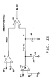
- FIG. 3A illustrates a circuit schematic of the first embodiment in this disclosure.
- An amplifier A1 80 has two inputs Vdd 81 and voltage reference Vref 82.
- a MUX 85 has two input signals Vdd and ground Vss 85, providing gain Gm1.
- a current of magnitude I Gm1 Vdd, for voltage V1.
- a switch RST 90 is a switch to ground. This is followed by a capacitor C 95 providing voltage V1.
- the two signals VTHRESH and V1 are inputs to comparator COMP1 100 providing an output signal Min Off.
- FIG. 3B illustrates a circuit schematic of the second embodiment in this disclosure.
- a second embodiment is to charge a capacitor with a current proportional to Vdd. If the circuit is arranged such that the capacitor must charge up to a voltage proportional to (Vdd-Vout) then the time taken will be proportional to the value required to remove the duty-cycle effect on the frequency of the buck. The buck converter will then operate with a fixed frequency when in continuous current mode operation.
- FIG. 3B creates a fixed current into the capacitor.
- the circuit implementation has a power supply Vdd 105.
- a first differential amplifier 110 has a negative input connected to input reference signal Vref.
- the first differential amplifier 110 has an output signal connected to a gate of a p-channel MOSFET 140.
- the first differential amplifier 110 positive input is electrically connected to the source of the p-channel MOSFET P1 140.
- the p-channel MOSFET P1 140 source is connected to a resistor element R1 151 and p-channel MOSFET 140 drain is connected to a resistor element R2 152.
- a second differential amplifier 120 has a negative input connected to a resistor divider resistor element R3 153 and resistor element R4 154.
- the second differential amplifier 120 has an output signal connected to a gate of p-channel MOSFET P2 150.
- the second differential amplifier 120 positive input is electrically connected to the source of the p-channel MOSFET 150.
- the p-channel MOSFET 140 source is connected to a resistor element R5 155 and p-channel MOSFET 150 drain is connected to a switch RST 156, and capacitor element C1 160.
- a comparator COMP1 130 has two inputs where the first positive input is connected to the p-channel MOSFET P1 drain 140, and a second negative input connected to the p-channel MOSFET P2 drain 150. The output of the comparator COMP1 130 is the "Min-off" signal 135.
- FIG. 4 is a circuit schematic diagram illustrating a circuit schematic in accordance with the third embodiment of the disclosure.
- the circuit as illustrated in FIG. 4 uses a resistor rather than a current source to reduce the quiescent current the block requires.
- the circuit below is similar to the first embodiment, but somewhat simpler.
- the current into the capacitor is no longer constant, but is still directly proportional to the supply.
- the initial slope of the voltage waveform on V1 will be approximately linear and proportional to the supply. Therefore if the threshold voltage is relatively low the circuit will approximate the first implementation. If the threshold is higher the voltage is no longer linear, but is still proportional to supply. In any practical implementation this circuit is sufficient to give a good fixed frequency operation.
- the circuit implementation has a power supply Vdd 105.
- a first differential amplifier 110 has a negative input connected to input signal reference voltage Vref.
- the first differential amplifier 110 has an output signal connected to a gate of a p-channel MOSFET 140.
- the first differential amplifier 110 positive input is electrically connected to the source of the p-channel MOSFET P1 140.
- the p-channel MOSFET P1 140 source is connected to a resistor element R1 151 and p-channel MOSFET 140 drain is connected to a resistor element R2 152.
- a comparator COMP1 130 has two inputs where the first positive input is connected to the p-channel MOSFET P1 drain 140, and a second negative input connected to a switch RST 156, and capacitor element C1 160.
- a second switch 170 is in series with the resistor 155.
- the output of comparator COMP1 130 is the "Min-off' signal 135.
- This invention fixes the frequency of the buck in PFM making the effect of the interference much easier to prevent in a practical design.
- the fixed frequency also offers other benefits in multi-phase bucks. Specifically it allows the use of a fixed delay between phases to create equally spaced phase delays. This radically simplifies the creation of multi-phase PFM bucks.
- the circuit in the second embodiment was designed and simulated with a full switching model of the PFM buck with dynamic sleep current.
- the table, Table 1, below shows the results obtained from the second embodiment.
- Table 1. Vin Vout Freq1 Freq2 4.7 0.6 2.41 2.08 4 0.6 2.34 2.06 3.2 0.6 2.24 2.05 4.7 1 2.17 2.08 4 1 2.07 2.07 3.2 1 1.90 2.04 4.7 1.4 1.94 2.08 4 1.4 1.79 2.06 3.2 1.4 1.55 2.01 Tol. 23% 1.68%
- the first two columns show the supply and output voltage. As these change so the duty cycle will change. As the duty cycle changes if the minimum off-time is fixed the frequency will shift.
- the expected frequency for a fixed minimum off-time implementation is given in the third column.
- the fourth column shows the results when using the circuit as shown. The tolerance is given at the bottom.
- the frequency of the fixed minimum off-time circuit is 2.07MHz +/-23%.
- the frequency of the proposed circuit is 2.07MHz +/-1.68%. This accuracy is more than adequate to create a multi-phase buck converter using just a simple delay circuit to offset each phase.
- the same effect is created in a digital or semi-digital way. For example, if the supply current were measured using an analog-to-digital converter, ADC, and if the minimum off-time were digitally programmable. In this case the digital would calculate the "correct" minimum off-time for the supply and output voltage conditions to give fixed frequency operation.
- ADC analog-to-digital converter
- the digital would calculate the "correct" minimum off-time for the supply and output voltage conditions to give fixed frequency operation.
- This embodiment can be applied to any combination of purely analog, purely digital or mixed-mode applications. Equally, the scheme should be suitable for most switching architectures that use a continuous-current mode of operation, and specifically should cover boost converters, as well as buck converters.
- FIG. 5 a methodology for providing an improved buck converter in pulse frequency modulation (PFM) mode in accordance with an embodiment of the disclosure.
- a method of pulse frequency modulation (PFM) with low loads comprises the steps: a first step 170 providing a buck converter having a pulse frequency modulation (PFM) mode, a second step 180 operating the PFM mode with a fixed frequency where the fixed frequency is set using a minimum off-time, a third step 190 setting the minimum off-time to be proportional to (1-D), where D is the duty cycle of the buck converter.
Landscapes
- Engineering & Computer Science (AREA)
- Power Engineering (AREA)
- Dc-Dc Converters (AREA)
Abstract
Description
- The disclosure relates generally to power supply circuits and methods and, more particularly, to buck type converters, circuit and a method thereof.
- DC-DC converters are voltage regulators used in conjunction with semiconductor devices, integrated circuit (IC), battery chargers, and other applications. DC-DC converters can be used in digital, analog, and power applications to deliver a regulated supply voltage.
- An example of known to the inventor, DC-DC converter's regulator output stage is shown in
FIG. 1. FIG. 1 illustrates a typical implementation of a buck DC/DC output stage supplying a resistive load. The circuit comprises of avoltage source VDD 10, andoutput voltage VOUT 20, a p-channel MOSFET switch 30, a n-channel MOSFET switch 40. Aninductor element 50 is electrically couples the switch network (p-channel MOSFET switch 30 and a n-channel MOSFET switch 40) and the output load (e.g. he output load consists ofa d capacitor 60 and resistive load 70). A buck converter generates a pulse width modulation (PWM) switching voltage at the LX node, denoted as VLX. This voltage is filtered, with high efficiency, by an inductor (L) 50, and an output capacitor (C) 60. Buck converters operate in one of two modes, the pulse width modulation (PWM) mode, and the pulse frequency modulation (PFM) mode. In the pulse width modulation (PWM) mode, the frequency of operation is fixed. In the pulse frequency modulation (PFM) mode, the frequency is allowed to change with the load current. - As illustrated in
FIG. 2 , the p-channel MOSFET switch voltage and inductor coil current are shown as a function of time is denoted. The p-channel MOSFET switch voltage as a function of time 74 highlights the voltage state during the on-time, off-time and period. The inductor coil current as a function oftime 76 also shows the current magnitude during the different states of the circuit. In both modes of operation, the inductor coil current (IL) increases during the on-time (Ton) when the p-channel MOSFET switch 30 is "on" state and the LX node is "high." During the off-time (Toff), the p-channel MOSFET switch 30 turns "off' state and the n-channel MOSFET switch 40 turns into an "on" state. During this state, the LX node goes to a " low state," and the inductor coil current (IL) decreases. The length of the operational cycle is the period, Tperiod, of the switching cycle that is the sum of the on-time (Ton), and the off-time (Toff). The frequency is related to the period, Tperiod. - Pulse frequency modulation (PFM) mode can be used to make a buck converter with superb operating characteristics. A buck converter in pulse frequency modulation (PFM) mode is stable with a variety of operating conditions and loads (e.g. output capacitor, output inductors, frequency, etc.). Additionally, the pulse frequency modulation (PFM) mode typically offers very low quiescent current, in comparison with a current-loop PWM mode buck converter. The pulse frequency modulation (PFM) mode naturally scales the frequency of the buck converter with load offering efficiency benefits at low and medium loads. However, PFM mode is not usually favored amongst system designers, as the noise created by the buck converter does not have a fixed frequency. This can cause issues with interference because the frequency is unpredictable. In pulse frequency modulation (PFM) architecture, the buck converter operates in PFM mode at low loads with a fixed current limit. As the load increases the current in the coil moves from discontinuous conduction mode (DCM) to continuous conduction mode (CCM). The frequency of the buck converter in this condition is set by the fixed minimum off-time. Once the load approaches the fixed current limit, the current limit is allowed to rise dynamically to support the load. The frequency is still set by the difference in the input and output voltages, and fixed minimum off-time.
- A digital pulse frequency modulation controller for switch-mode power supply is described. As discussed in published
U. S. Patent 8,525,502 to Weinstein et al , describes digital logic using a pulse frequency mode which includes a frequency targeting mode which dynamically adjusts the size of the pulses in order to achieve a switching frequency within a desired band. - A digital boost feedback voltage controller for switch-mode power supply using pulse frequency modulation (PF) described. As discussed in published
U. S. Patent 8,362,756 to Weinstein et al , discloses a controller configured to send pulse frequency modulation (PFM) high and low side signals that control the voltage on the power stage output capacitor and charge pump output capacitor. - A cascade boost and inverting buck converter with independent control has been disclosed. As discussed in published U. S. Patent Application
US 2012/03196046 to Walters - A current mode buck converter with fixed PWM/PFM boundary is disclosed. As discussed in published
U.S. Patent 8,106,642 and U.S Patent ApplicationUS2011/0241641 to Chen et al. , describes a buck converter that operates in pulse width modulation (PWM) and pulse frequency modulation (PFM) mode which transitions from PWM to PFM mode by adaptively adjusting a trigger condition. - In these embodiments, the solutions to improve the response of a voltage converter in pulse frequency modulation (PFM) mode , and more specifically utilize various means to address transitioning from PWM to PFM mode is discussed.
- It is desirable to provide a solution to that achieves a more predictable frequency for the buck converter in pulse frequency modulation (PFM) mode when the load current is high enough to create significant interference.
- It is desirable to provide a solution for a buck converter which operates in a purely hysteretic mode.
- It is desirable to provide a solution for a buck converter which operates in pulse frequency modulation (PFM) mode.
- It is desirable to provide a solution for a buck converter which operates in a continuous conduction mode (CCM).
- A principal object of the present disclosure is to provide a solution for a buck converter whose frequency becomes fixed by the minimum off-time at high loads.
- Another further object of the present disclosure is to provide a solution for a buck converter whose minimum off-time is set by a circuit to fix the value of the frequency.
- Also in accordance with the object of the present disclosure, an off-time circuit is provided that creates a minimum off-time proportional to (1-D) where D is the duty cycle.
- The above and other objects are achieved by a buck converter device in pulse frequency modulation (PFM) mode to provide a more predictable frequency.
- The above and other objects are further achieved by providing a buck converter having a pulse frequency modulation (PFM) mode where the frequency is fixed, where the fixed frequency is set using a minimum off-time, where the minimum off-time is proportional to 1-D where D is the duty cycle.
- The above and other objects are further achieved by a buck converter device having a pulse frequency modulation (PFM) where the frequency is fixed, with minimum off-time operation, whose minimum off time is proportional to the 1-D, where D is the duty cycle, the device comprising a comparator providing an output signal of a minimum off time, an amplifier; and, a p-channel MOSFET whose gate is connected to the output of said amplifier providing a signal threshold voltage to a positive terminal of said comparator.
- The above and other objects are further achieved by a method of pulse frequency modulation (PFM) with low loads, comprising the following steps: providing a buck converter having a PFM mode, operating said PFM mode with a fixed frequency, wherein the fixed frequency is set using a minimum off-time, and setting the minimum off-time to be proportional to (1-D), where D is a duty cycle of the buck converter.
- The above and other objects are further achieved by a method of pulse frequency modulation (PFM) with low loads comprising of the following steps: (1) providing a buck converter comprising of an amplifier, a comparator , a p-channel MOSFET, a first resistor element, a second resistor element, a third resistor element, a capacitor element, a first switch, and a second switch, (2) creating a replica of reference voltage Vref proportional to the difference between Vdd and Vref, (3) creating a threshold voltage above ground proportional to the difference between Vdd and Vref, (4) establishing a voltage on a capacitor whose rate of change is proportional to power supply Vdd, (5) establishing a time to charge a capacitor to a threshold voltage proportional to (Vdd-Vref)/Vdd, and (6) establishing a minimum off time on the output of a comparator.
- As such, a novel buck converter with improved pulse frequency modulation (PFM) mode of operation where the frequency is fixed is desired. Other advantages will be recognized by those of ordinary skill in the art.
- The present disclosure and the corresponding advantages and features provided thereby will be best understood and appreciated upon review of the following detailed description of the disclosure, taken in conjunction with the following drawings, where like numerals represent like elements, in which:
-
FIG. 1 is a circuit schematic diagram illustrating an embodiment known to the inventor of a buck converter and load; -
FIG. 2 is a plot of p-channel MOSFET switch voltage and coil current as a function of time known to the inventor; -
FIG. 3A is a circuit schematic diagram in accordance with a first embodiment of the disclosure; -
FIG. 3B is a circuit schematic diagram in accordance with a second embodiment of the disclosure; -
FIG. 4 is a circuit schematic diagram in accordance with a third embodiment of the disclosure; and -
FIG. 5 a methodology for providing an improved buck converter in pulse frequency modulation (PFM) mode in accordance with an embodiment of the disclosure. -
FIG. 1 illustrates a typical implementation of a buck DC/DC output stage supplying a resistive load. The circuit comprises of avoltage source VDD 10, andoutput voltage VOUT 20, a p-channel MOSFET switch 30, a n-channel MOSFET switch 40. Aninductor element 50 is electrically couples the switch network (p-channel MOSFET switch 30 and a n-channel MOSFET switch 40) and the output load (e.g. the output load consists of acapacitor 60 and resistive load 70). A buck converter generates a pulse width modulation (PWM) switching voltage at the LX node, denoted as VLX. This voltage is filtered, with high efficiency, by an inductor (L) 50, and an output capacitor (C) 60. Buck converters operate in one of two modes, the pulse width modulation (PWM) mode, and the pulse frequency modulation (PFM) mode. In the pulse width modulation (PWM) mode, the frequency of operation is fixed. In the pulse frequency modulation (PFM) mode, the frequency is allowed to change with the load current. - As illustrated in
FIG. 2 , the p-channel MOSFET switch voltage and inductor coil current are shown as a function of time is denoted as 80. The p-channel MOSFET switch voltage as a function of time 74 highlights the voltage state during the on-time, off-time and period. The inductor coil current as a function oftime 76 also shows the current magnitude during the different states of the circuit. In both modes of operation, the inductor coil current (IL) increases during the on-time (Ton) when the p-channel MOSFET switch 30 is "on" state and the LX node is "high." During the off-time (Toff), the p-channel MOSFET switch 30 turns "off' state and the n-channel MOSFET switch 40 turns into an "on" state. During this state, the LX node goes to a "low state," and the inductor coil current (IL) decreases. The length of the operational cycle is the period, Tperiod, of the switching cycle that is the sum of the on-time (Ton), and the off-time (Toff). The frequency is related to the period, Tperiod. - The buck converter may operate in pure PFM with low loads. In this mode the buck converter operates as follows ; (1) When the output voltage falls below the reference voltage the output PMOS turns on; (2) When the current in the coil reaches the fixed current limit the output PMOS turns off and the output NMOS turns on; (3) If the NMOS current reaches zero, before the output voltage falls below the reference voltage again, both pass-devices are turned off and the output is high impedance; (4) When the load current approaches the fixed current limit the buck moves to "dynamic sleep". In this mode the current limit is varied with the drop in output voltage of the buck. When the buck is operating in this mode the frequency is fixed by the minimum off-time. In this case the buck operates as follows: (A) The output voltage is always below the DAC voltage, so the PMOS turns on immediately; (B) The current rises until it reaches the dynamically controlled current limit; (C) The NMOS turns on, and the minimum off-time counter is started: (D) Once the minimum off-time counter completes the PMOS turns back on
The duty cycle of the buck is still such that Ton=Tperiod*(D) and Toff=Tperiod*(1-D) where D is the duty cycle, D=(vout/Vdd). If the output voltage (vout) and the supply (Vdd) are fixed, the frequency is therefore controlled by the minimum off-time. If the minimum off time is controlled so that Toff = K(1-D) where K is a constant then the frequency is fixed (again D = Vout/Vdd). To explain what happens here consider the case where supply rises and the min off-time is fixed. As the supply rises so the rate of change of current in the coil during the NMOS on-time increases. The minimum current in the coil (below the current limit) therefore falls. The rate of change of current in the coil for the PMOS on-time has not changed, so the PMOS on time must be longer. This causes the frequency to fall. With the variable min-off time as given above the effect is countered. Now, as supply rises the min off-time decreased, and so the frequency remains the same. By expanding the equation a practical circuit can be found. Toff = K.(Vdd-Vout)/Vdd -
FIG. 3A illustrates a circuit schematic of the first embodiment in this disclosure. Anamplifier A1 80 has twoinputs Vdd 81 andvoltage reference Vref 82. The output of amplifier A1 80value is the VTHRESH , where is VTHRESH = A1 * (Vdd -Vref). AMUX 85 has two input signals Vdd andground Vss 85, providing gain Gm1. A current of magnitude I = Gm1 Vdd, for voltage V1. Aswitch RST 90 is a switch to ground. This is followed by acapacitor C 95 providing voltage V1. The two signals VTHRESH and V1 are inputs tocomparator COMP1 100 providing an output signal Min Off. -
FIG. 3B illustrates a circuit schematic of the second embodiment in this disclosure. A second embodiment is to charge a capacitor with a current proportional to Vdd. If the circuit is arranged such that the capacitor must charge up to a voltage proportional to (Vdd-Vout) then the time taken will be proportional to the value required to remove the duty-cycle effect on the frequency of the buck. The buck converter will then operate with a fixed frequency when in continuous current mode operation.FIG. 3B creates a fixed current into the capacitor. The circuit implementation has apower supply Vdd 105. A firstdifferential amplifier 110 has a negative input connected to input reference signal Vref. The firstdifferential amplifier 110 has an output signal connected to a gate of a p-channel MOSFET 140. The firstdifferential amplifier 110 positive input is electrically connected to the source of the p-channel MOSFET P1 140. The p-channel MOSFET P1 140 source is connected to aresistor element R1 151 and p-channel MOSFET 140 drain is connected to aresistor element R2 152. A seconddifferential amplifier 120 has a negative input connected to a resistor dividerresistor element R3 153 andresistor element R4 154. The seconddifferential amplifier 120 has an output signal connected to a gate of p-channel MOSFET P2 150. The seconddifferential amplifier 120 positive input is electrically connected to the source of the p-channel MOSFET 150. The p-channel MOSFET 140 source is connected to aresistor element R5 155 and p-channel MOSFET 150 drain is connected to aswitch RST 156, andcapacitor element C1 160. Acomparator COMP1 130 has two inputs where the first positive input is connected to the p-channelMOSFET P1 drain 140, and a second negative input connected to the p-channelMOSFET P2 drain 150. The output of thecomparator COMP1 130 is the "Min-off"signal 135. - In the circuit above the operation is as follows:
- The amplifier AMP1 creates a replica of Vref at the bottom of R1. The current through R1 is therefore proportional to the difference between Vdd and Vref. This is the (Vdd-Vref) term in the equation.
- This current is passed through R2, creating a threshold voltage (Vthresh) above ground proportional to Vdd-Vref. The resistors R3 and R4 create a voltage proportional to Vdd.
- The amplifier AMP2 creates a replica of this voltage across R5 equal to that across R3. The current through R5 is therefore proportional to the supply voltage Vdd.
- The rate of change of the voltage across C1 is therefore proportional also to Vdd.
- The time taken for the capacitor C1 to charge to Vthresh is therefore proportional to:

-
FIG. 4 is a circuit schematic diagram illustrating a circuit schematic in accordance with the third embodiment of the disclosure. The circuit as illustrated inFIG. 4 uses a resistor rather than a current source to reduce the quiescent current the block requires. The circuit below is similar to the first embodiment, but somewhat simpler. The current into the capacitor is no longer constant, but is still directly proportional to the supply. The initial slope of the voltage waveform on V1 will be approximately linear and proportional to the supply. Therefore if the threshold voltage is relatively low the circuit will approximate the first implementation. If the threshold is higher the voltage is no longer linear, but is still proportional to supply. In any practical implementation this circuit is sufficient to give a good fixed frequency operation. - The circuit implementation has a
power supply Vdd 105. A firstdifferential amplifier 110 has a negative input connected to input signal reference voltage Vref. The firstdifferential amplifier 110 has an output signal connected to a gate of a p-channel MOSFET 140. The firstdifferential amplifier 110 positive input is electrically connected to the source of the p-channel MOSFET P1 140. The p-channel MOSFET P1 140 source is connected to aresistor element R1 151 and p-channel MOSFET 140 drain is connected to aresistor element R2 152. Acomparator COMP1 130 has two inputs where the first positive input is connected to the p-channelMOSFET P1 drain 140, and a second negative input connected to aswitch RST 156, andcapacitor element C1 160. Asecond switch 170 is in series with theresistor 155. The output ofcomparator COMP1 130 is the "Min-off'signal 135. - This invention fixes the frequency of the buck in PFM making the effect of the interference much easier to prevent in a practical design. The fixed frequency also offers other benefits in multi-phase bucks. Specifically it allows the use of a fixed delay between phases to create equally spaced phase delays. This radically simplifies the creation of multi-phase PFM bucks.
- The circuit in the second embodiment was designed and simulated with a full switching model of the PFM buck with dynamic sleep current. The table, Table 1, below shows the results obtained from the second embodiment.
Table 1. Vin Vout Freq1 Freq2 4.7 0.6 2.41 2.08 4 0.6 2.34 2.06 3.2 0.6 2.24 2.05 4.7 1 2.17 2.08 4 1 2.07 2.07 3.2 1 1.90 2.04 4.7 1.4 1.94 2.08 4 1.4 1.79 2.06 3.2 1.4 1.55 2.01 Tol. 23% 1.68% - The first two columns show the supply and output voltage. As these change so the duty cycle will change. As the duty cycle changes if the minimum off-time is fixed the frequency will shift. The expected frequency for a fixed minimum off-time implementation is given in the third column. The fourth column shows the results when using the circuit as shown. The tolerance is given at the bottom. The frequency of the fixed minimum off-time circuit is 2.07MHz +/-23%. The frequency of the proposed circuit is 2.07MHz +/-1.68%. This accuracy is more than adequate to create a multi-phase buck converter using just a simple delay circuit to offset each phase.
- The same effect is created in a digital or semi-digital way. For example, if the supply current were measured using an analog-to-digital converter, ADC, and if the minimum off-time were digitally programmable. In this case the digital would calculate the "correct" minimum off-time for the supply and output voltage conditions to give fixed frequency operation. This embodiment, can be applied to any combination of purely analog, purely digital or mixed-mode applications. Equally, the scheme should be suitable for most switching architectures that use a continuous-current mode of operation, and specifically should cover boost converters, as well as buck converters.
-
FIG. 5 a methodology for providing an improved buck converter in pulse frequency modulation (PFM) mode in accordance with an embodiment of the disclosure. A method of pulse frequency modulation (PFM) with low loads comprises the steps: afirst step 170 providing a buck converter having a pulse frequency modulation (PFM) mode, asecond step 180 operating the PFM mode with a fixed frequency where the fixed frequency is set using a minimum off-time, athird step 190 setting the minimum off-time to be proportional to (1-D), where D is the duty cycle of the buck converter. - As such, a novel buck converter with fixed frequency operation and minimum off-time are herein described. Other advantages will be recognized by those of ordinary skill in the art.
- The above detailed description of the disclosure, and the examples described therein, has been presented for the purposes of illustration and description. While the principles of the disclosure have been described above in connection with a specific device, it is to be clearly understood that this description is made only by way of example and not as a limitation on the scope of the disclosure.
Claims (17)
- A buck converter device having a pulse frequency modulation (PFM) where the frequency is fixed using a minimum off-time operation, where the minimum off time is proportional to the 1-D, wherein D is the duty cycle.
- The buck converter of claim 1 , the device comprising:- a comparator providing an output signal of a minimum off time;- a first amplifier;- a p-channel MOSFET whose gate is connected to the output of said first amplifier providing a signal threshold voltage to a positive terminal of said comparator;- a second amplifier; and,- a second p-channel MOSFET whose gate is connected to the output of said second amplifier providing a signal to a negative terminal of said comparator.
- The buck converter of claim 2, wherein the negative input terminal of said first amplifier is the reference voltage Vref, and wherein the positive input of said first amplifier is electrically connected to a first resistor and said first p-channel MOSFET source, and wherein said first p-channel MOSFET drain is electrically connected to a second resistor element and providing a positive threshold voltage input to said comparator whose threshold voltage is proportional to the difference between the power supply voltage Vdd and reference voltage Vref, and wherein said second amplifier negative input is electrically connected to a resistor divider network further comprising a third resistor and a fourth resistor providing a voltage to said negative input proportional to the power supply voltage.
- The buck converter of claim 3, wherein said comparator negative input is electrically connected to a switch providing a the start of the on-time to allow for re-initiation at the next off-time; and wherein said comparator negative input is electrically connected to a capacitor providing a rate of change across the capacitor is proportional to the power supply voltage Vdd.
- The buck converter of claim 4, wherein said capacitor is charged to the threshold voltage is the time proportional to (Vdd-Vref)/Vdd.
- A buck converter device having a pulse frequency modulation (PFM) where the frequency is fixed, with minimum off-time operation, whose minimum off time is proportional to the 1-D, where D is the duty cycle, the device comprising:- a comparator providing an output signal of a minimum off time;- a first amplifier; and,- a p-channel MOSFET whose gate is connected to the output of said first amplifier providing a signal threshold voltage to a positive terminal of said comparator.
- The buck converter of claim 2 or 6 wherein the negative input terminal of said first amplifier is the reference voltage Vref.
- The buck converter of claim 7, wherein the positive input of said amplifier is electrically connected to a first resistor and said first p-channel MOSFET source.
- The buck converter of claim 8, wherein said first p-channel MOSFET drain is electrically connected to a second resistor element and providing a positive threshold voltage input to said comparator whose threshold voltage is proportional to the difference between the power supply voltage Vdd and reference voltage Vref.
- The buck converter of claim 3 or 9, wherein said comparator negative input is electrically connected to a switch providing a the start of the on-time to allow for re-initiation at the next off-time.
- The buck converter of claim 10, wherein said comparator negative input is electrically connected to a capacitor of voltage V1 providing a rate of change across the capacitor is linear and proportional to the power supply voltage Vdd.
- The buck converter of claim 11, wherein said comparator negative input is electrically connected to a series combination of a resistor and a switch.
- The buck converter of claim 12, wherein said converter provides a fixed frequency operation.
- A method of pulse frequency modulation (PFM) with low loads, comprising the following steps:- providing a buck converter having a PFM mode;- operating said PFM mode with a fixed frequency, wherein the fixed frequency is set using a minimum off-time; and- setting the minimum off time to be proportional to (1-D), where D is a duty cycle of the buck converter.
- The method of pulse frequency modulation (PFM) of claim 14 further comprising of the following steps :- providing a buck converter comprising of a first amplifier, a second amplifier, and a comparator , a first p-channel MOSFET, a second p-channel MOSFET (PMOS), a first resistor element, a second resistor element, a third resistor element, a fourth resistor element, a capacitor element, and a switch;- creating a replica of the reference voltage Vref proportional to the difference between Vdd and Vref;- creating a threshold voltage above ground proportional to the difference between Vdd and Vref;- establishing a voltage from said third resistor and said fourth resistor proportional to power supply Vdd on said second amplifier;- creating a replica of the voltage on said fifth resistor equal to the voltage across said third resistor proportional to the supply voltage Vdd;- establishing a voltage on said capacitor whose rate of change is proportional to power supply Vdd;- establishing a time to charge the capacitor to a threshold voltage proportional to (Vdd-Vref)/Vdd; and- establishing a minimum off- time on the output of said comparator.
- The method of pulse frequency modulation (PFM) of claim 15 further comprising the steps:resetting the switch at the start time of the on-time.
- A method of pulse frequency modulation (PFM) with low loads comprising of the following steps:- providing a buck converter comprising of an amplifier, a comparator, a p-channel MOSFET, a first resistor element, a second resistor element, a third resistor element, a capacitor element, a first switch, and a second switch;- creating a replica of reference voltage Vref proportional to the difference between Vdd and Vref;- creating a threshold voltage above ground proportional to the difference between Vdd and Vref;- establishing a voltage on said capacitor whose rate of change is proportional to power supply Vdd;- establishing a time to charge the capacitor to a threshold voltage proportional to (Vdd-Vref)/Vdd; and- establishing a minimum off time on the output of said comparator.
Priority Applications (2)
| Application Number | Priority Date | Filing Date | Title |
|---|---|---|---|
| EP14188907.1A EP3010151B1 (en) | 2014-10-14 | 2014-10-14 | Method and apparatus for a buck converter with pulse width modulation and pulse frequency modulation mode |
| US14/516,820 US10103720B2 (en) | 2014-10-14 | 2014-10-17 | Method and apparatus for a buck converter with pulse width modulation and pulse frequency modulation mode |
Applications Claiming Priority (1)
| Application Number | Priority Date | Filing Date | Title |
|---|---|---|---|
| EP14188907.1A EP3010151B1 (en) | 2014-10-14 | 2014-10-14 | Method and apparatus for a buck converter with pulse width modulation and pulse frequency modulation mode |
Publications (2)
| Publication Number | Publication Date |
|---|---|
| EP3010151A1 true EP3010151A1 (en) | 2016-04-20 |
| EP3010151B1 EP3010151B1 (en) | 2020-09-02 |
Family
ID=51690955
Family Applications (1)
| Application Number | Title | Priority Date | Filing Date |
|---|---|---|---|
| EP14188907.1A Active EP3010151B1 (en) | 2014-10-14 | 2014-10-14 | Method and apparatus for a buck converter with pulse width modulation and pulse frequency modulation mode |
Country Status (2)
| Country | Link |
|---|---|
| US (1) | US10103720B2 (en) |
| EP (1) | EP3010151B1 (en) |
Families Citing this family (7)
| Publication number | Priority date | Publication date | Assignee | Title |
|---|---|---|---|---|
| US9906128B2 (en) | 2014-10-29 | 2018-02-27 | Infineon Technologies Austria Ag | Intermediate voltage bus converter with power saving modes |
| US9735678B2 (en) * | 2015-09-04 | 2017-08-15 | Dialog Semiconductor (Uk) Limited | Voltage converters with asymmetric gate voltages |
| CN106208692B (en) * | 2016-08-31 | 2020-05-22 | 杰华特微电子(杭州)有限公司 | Switch circuit control method, control circuit and switch circuit device |
| US11152846B2 (en) | 2020-01-15 | 2021-10-19 | Apple Inc. | Method and apparatus for providing adaptive inductor peak current in DC-DC converter |
| CN113162407B (en) * | 2021-03-26 | 2023-03-24 | 西安电子科技大学 | Step-down DC-DC converter with ultra-low static power consumption |
| US20240421690A1 (en) * | 2023-06-13 | 2024-12-19 | Texas Instruments Incorporated | Dynamic minimum off-time for switching regulator |
| CN117294161B (en) * | 2023-11-24 | 2024-02-09 | 湖南科技大学 | Method for determining stable domain of main circuit parameters of Buck-Boost inverter based on medium frequency state |
Citations (7)
| Publication number | Priority date | Publication date | Assignee | Title |
|---|---|---|---|---|
| US20080024104A1 (en) * | 2006-07-25 | 2008-01-31 | Fuji Electric Device Technology Co., Ltd. | DC-DC converter |
| KR20100102824A (en) * | 2009-03-12 | 2010-09-27 | 한양대학교 산학협력단 | Adaptive on-time controller and pulse frequency modulation buck converter using the same |
| US20110241641A1 (en) | 2010-04-06 | 2011-10-06 | Chih-Ning Chen | Current Mode Buck Converter with Fixed PWM/PFM Boundary |
| US20120319604A1 (en) | 2011-06-17 | 2012-12-20 | Intersil Americas Inc. | Cascade boost and inverting buck converter with independent control |
| US8362756B2 (en) | 2010-12-21 | 2013-01-29 | Exar Corporation | Digital boost feedback voltage controller for switch-mode power supplies using pulse-frequency modulation |
| US8525502B2 (en) | 2011-03-02 | 2013-09-03 | Exar Corporation | Digital pulse-frequency modulation controller for switch-mode power supplies with frequency targeting and ultrasonic modes |
| US20140232367A1 (en) * | 2013-02-20 | 2014-08-21 | Anpec Electronics Corporation | Switching regulator control method |
Family Cites Families (6)
| Publication number | Priority date | Publication date | Assignee | Title |
|---|---|---|---|---|
| US6900995B2 (en) * | 2001-11-29 | 2005-05-31 | Iwatt, Inc. | PWM power converter controlled by transistion detection of a comparator error signal |
| JP5255908B2 (en) * | 2008-05-27 | 2013-08-07 | ルネサスエレクトロニクス株式会社 | Semiconductor integrated circuit and operation method thereof |
| US8164218B2 (en) * | 2008-07-17 | 2012-04-24 | Monolithic Power Systems, Inc. | Power converters and associated methods of control |
| US8476882B2 (en) * | 2010-09-30 | 2013-07-02 | Exar Corporation | Reference voltage based equivalent series resistance (ESR) emulation for constant on-time (COT) control of buck regulators |
| US8552706B2 (en) * | 2011-03-29 | 2013-10-08 | Analog Devices, Inc. | Stability methods and structures for current-mode DC-DC voltage converters |
| JP5703950B2 (en) * | 2011-05-13 | 2015-04-22 | 富士電機株式会社 | Voltage-current converter |
-
2014
- 2014-10-14 EP EP14188907.1A patent/EP3010151B1/en active Active
- 2014-10-17 US US14/516,820 patent/US10103720B2/en not_active Expired - Fee Related
Patent Citations (8)
| Publication number | Priority date | Publication date | Assignee | Title |
|---|---|---|---|---|
| US20080024104A1 (en) * | 2006-07-25 | 2008-01-31 | Fuji Electric Device Technology Co., Ltd. | DC-DC converter |
| KR20100102824A (en) * | 2009-03-12 | 2010-09-27 | 한양대학교 산학협력단 | Adaptive on-time controller and pulse frequency modulation buck converter using the same |
| US20110241641A1 (en) | 2010-04-06 | 2011-10-06 | Chih-Ning Chen | Current Mode Buck Converter with Fixed PWM/PFM Boundary |
| US8106642B2 (en) | 2010-04-06 | 2012-01-31 | Anpec Electronics Corporation | Current mode buck converter with fixed PWM/PFM boundary |
| US8362756B2 (en) | 2010-12-21 | 2013-01-29 | Exar Corporation | Digital boost feedback voltage controller for switch-mode power supplies using pulse-frequency modulation |
| US8525502B2 (en) | 2011-03-02 | 2013-09-03 | Exar Corporation | Digital pulse-frequency modulation controller for switch-mode power supplies with frequency targeting and ultrasonic modes |
| US20120319604A1 (en) | 2011-06-17 | 2012-12-20 | Intersil Americas Inc. | Cascade boost and inverting buck converter with independent control |
| US20140232367A1 (en) * | 2013-02-20 | 2014-08-21 | Anpec Electronics Corporation | Switching regulator control method |
Non-Patent Citations (1)
| Title |
|---|
| CHEN-YU WANG ET AL: "A high effieciency DC/DC boost regulator with adaptive off/on-time control", VLSI DESIGN, AUTOMATION, AND TEST (VLSI-DAT), 2013 INTERNATIONAL SYMPOSIUM ON, IEEE, 22 April 2013 (2013-04-22), pages 1 - 4, XP032679852, ISBN: 978-1-4673-4435-7, [retrieved on 20130614], DOI: 10.1109/VLDI-DAT.2013.6533804 * |
Also Published As
| Publication number | Publication date |
|---|---|
| US20160105108A1 (en) | 2016-04-14 |
| US10103720B2 (en) | 2018-10-16 |
| EP3010151B1 (en) | 2020-09-02 |
Similar Documents
| Publication | Publication Date | Title |
|---|---|---|
| US9035638B2 (en) | DC/DC converter arrangement and method for DC/DC conversion | |
| US11444537B2 (en) | Power converters and compensation circuits thereof | |
| US10594215B2 (en) | Circuits and methods to linearize conversion gain in a DC-DC converter | |
| US20210067041A1 (en) | Buck converter including inductor current sensing via high- and low-side switching device current sensing | |
| CN109586565B (en) | COT controlled multiphase direct current converter, control circuit and current sharing method | |
| US10566901B2 (en) | Constant-frequency control method with fast transient | |
| EP3010151B1 (en) | Method and apparatus for a buck converter with pulse width modulation and pulse frequency modulation mode | |
| US9312772B2 (en) | Current limiting scheme for a converter | |
| US10250122B2 (en) | Multi-phase control for pulse width modulation power converters | |
| US8148967B2 (en) | PWM clock generation system and method to improve transient response of a voltage regulator | |
| US9529373B2 (en) | Switching regulator and control circuit and control method therefor | |
| CN105450024B (en) | Multi-stage amplifier | |
| US8063615B2 (en) | Synchronous rectifier control for synchronous boost converter | |
| CN106464265B (en) | DC-DC Converter Controller Device with Dual Counter Digital Integrator | |
| CN106849650B (en) | Method and system for reducing transients in DC-DC converters | |
| EP2973971B1 (en) | Systems and methods for 100 percent duty cycle in switching regulators | |
| US8502516B2 (en) | Voltage adjustment module and power supply device | |
| US20050017703A1 (en) | Synthetic ripple regulator | |
| US20070085523A1 (en) | Dc-dc converter | |
| US8164218B2 (en) | Power converters and associated methods of control | |
| CN105337500A (en) | Power converter and method for adjusting linear transient response of power converter | |
| JP2013165537A (en) | Switching regulator, control method therefor, and power supply device | |
| KR101289727B1 (en) | A charge pump circuit controlling output voltage by RC time constant | |
| US9490699B2 (en) | Digitally controlled current mode power converter | |
| US9081403B1 (en) | Optimal compensating ramp generator for fixed frequency current mode DC-DC converters |
Legal Events
| Date | Code | Title | Description |
|---|---|---|---|
| PUAI | Public reference made under article 153(3) epc to a published international application that has entered the european phase |
Free format text: ORIGINAL CODE: 0009012 |
|
| AK | Designated contracting states |
Kind code of ref document: A1 Designated state(s): AL AT BE BG CH CY CZ DE DK EE ES FI FR GB GR HR HU IE IS IT LI LT LU LV MC MK MT NL NO PL PT RO RS SE SI SK SM TR |
|
| AX | Request for extension of the european patent |
Extension state: BA ME |
|
| 17P | Request for examination filed |
Effective date: 20161020 |
|
| RBV | Designated contracting states (corrected) |
Designated state(s): AL AT BE BG CH CY CZ DE DK EE ES FI FR GB GR HR HU IE IS IT LI LT LU LV MC MK MT NL NO PL PT RO RS SE SI SK SM TR |
|
| STAA | Information on the status of an ep patent application or granted ep patent |
Free format text: STATUS: REQUEST FOR EXAMINATION WAS MADE |
|
| STAA | Information on the status of an ep patent application or granted ep patent |
Free format text: STATUS: EXAMINATION IS IN PROGRESS |
|
| 17Q | First examination report despatched |
Effective date: 20180809 |
|
| RAP1 | Party data changed (applicant data changed or rights of an application transferred) |
Owner name: APPLE INC. |
|
| GRAP | Despatch of communication of intention to grant a patent |
Free format text: ORIGINAL CODE: EPIDOSNIGR1 |
|
| STAA | Information on the status of an ep patent application or granted ep patent |
Free format text: STATUS: GRANT OF PATENT IS INTENDED |
|
| INTG | Intention to grant announced |
Effective date: 20200317 |
|
| GRAS | Grant fee paid |
Free format text: ORIGINAL CODE: EPIDOSNIGR3 |
|
| GRAA | (expected) grant |
Free format text: ORIGINAL CODE: 0009210 |
|
| STAA | Information on the status of an ep patent application or granted ep patent |
Free format text: STATUS: THE PATENT HAS BEEN GRANTED |
|
| AK | Designated contracting states |
Kind code of ref document: B1 Designated state(s): AL AT BE BG CH CY CZ DE DK EE ES FI FR GB GR HR HU IE IS IT LI LT LU LV MC MK MT NL NO PL PT RO RS SE SI SK SM TR |
|
| REG | Reference to a national code |
Ref country code: GB Ref legal event code: FG4D |
|
| REG | Reference to a national code |
Ref country code: AT Ref legal event code: REF Ref document number: 1309989 Country of ref document: AT Kind code of ref document: T Effective date: 20200915 Ref country code: CH Ref legal event code: EP |
|
| REG | Reference to a national code |
Ref country code: DE Ref legal event code: R096 Ref document number: 602014069619 Country of ref document: DE |
|
| REG | Reference to a national code |
Ref country code: IE Ref legal event code: FG4D |
|
| REG | Reference to a national code |
Ref country code: LT Ref legal event code: MG4D |
|
| PG25 | Lapsed in a contracting state [announced via postgrant information from national office to epo] |
Ref country code: SE Free format text: LAPSE BECAUSE OF FAILURE TO SUBMIT A TRANSLATION OF THE DESCRIPTION OR TO PAY THE FEE WITHIN THE PRESCRIBED TIME-LIMIT Effective date: 20200902 Ref country code: NO Free format text: LAPSE BECAUSE OF FAILURE TO SUBMIT A TRANSLATION OF THE DESCRIPTION OR TO PAY THE FEE WITHIN THE PRESCRIBED TIME-LIMIT Effective date: 20201202 Ref country code: BG Free format text: LAPSE BECAUSE OF FAILURE TO SUBMIT A TRANSLATION OF THE DESCRIPTION OR TO PAY THE FEE WITHIN THE PRESCRIBED TIME-LIMIT Effective date: 20201202 Ref country code: GR Free format text: LAPSE BECAUSE OF FAILURE TO SUBMIT A TRANSLATION OF THE DESCRIPTION OR TO PAY THE FEE WITHIN THE PRESCRIBED TIME-LIMIT Effective date: 20201203 Ref country code: LT Free format text: LAPSE BECAUSE OF FAILURE TO SUBMIT A TRANSLATION OF THE DESCRIPTION OR TO PAY THE FEE WITHIN THE PRESCRIBED TIME-LIMIT Effective date: 20200902 Ref country code: HR Free format text: LAPSE BECAUSE OF FAILURE TO SUBMIT A TRANSLATION OF THE DESCRIPTION OR TO PAY THE FEE WITHIN THE PRESCRIBED TIME-LIMIT Effective date: 20200902 Ref country code: FI Free format text: LAPSE BECAUSE OF FAILURE TO SUBMIT A TRANSLATION OF THE DESCRIPTION OR TO PAY THE FEE WITHIN THE PRESCRIBED TIME-LIMIT Effective date: 20200902 |
|
| PGFP | Annual fee paid to national office [announced via postgrant information from national office to epo] |
Ref country code: DE Payment date: 20200929 Year of fee payment: 7 |
|
| REG | Reference to a national code |
Ref country code: NL Ref legal event code: MP Effective date: 20200902 |
|
| REG | Reference to a national code |
Ref country code: AT Ref legal event code: MK05 Ref document number: 1309989 Country of ref document: AT Kind code of ref document: T Effective date: 20200902 |
|
| PG25 | Lapsed in a contracting state [announced via postgrant information from national office to epo] |
Ref country code: PL Free format text: LAPSE BECAUSE OF FAILURE TO SUBMIT A TRANSLATION OF THE DESCRIPTION OR TO PAY THE FEE WITHIN THE PRESCRIBED TIME-LIMIT Effective date: 20200902 Ref country code: RS Free format text: LAPSE BECAUSE OF FAILURE TO SUBMIT A TRANSLATION OF THE DESCRIPTION OR TO PAY THE FEE WITHIN THE PRESCRIBED TIME-LIMIT Effective date: 20200902 Ref country code: LV Free format text: LAPSE BECAUSE OF FAILURE TO SUBMIT A TRANSLATION OF THE DESCRIPTION OR TO PAY THE FEE WITHIN THE PRESCRIBED TIME-LIMIT Effective date: 20200902 |
|
| PG25 | Lapsed in a contracting state [announced via postgrant information from national office to epo] |
Ref country code: CZ Free format text: LAPSE BECAUSE OF FAILURE TO SUBMIT A TRANSLATION OF THE DESCRIPTION OR TO PAY THE FEE WITHIN THE PRESCRIBED TIME-LIMIT Effective date: 20200902 Ref country code: EE Free format text: LAPSE BECAUSE OF FAILURE TO SUBMIT A TRANSLATION OF THE DESCRIPTION OR TO PAY THE FEE WITHIN THE PRESCRIBED TIME-LIMIT Effective date: 20200902 Ref country code: PT Free format text: LAPSE BECAUSE OF FAILURE TO SUBMIT A TRANSLATION OF THE DESCRIPTION OR TO PAY THE FEE WITHIN THE PRESCRIBED TIME-LIMIT Effective date: 20210104 Ref country code: NL Free format text: LAPSE BECAUSE OF FAILURE TO SUBMIT A TRANSLATION OF THE DESCRIPTION OR TO PAY THE FEE WITHIN THE PRESCRIBED TIME-LIMIT Effective date: 20200902 Ref country code: RO Free format text: LAPSE BECAUSE OF FAILURE TO SUBMIT A TRANSLATION OF THE DESCRIPTION OR TO PAY THE FEE WITHIN THE PRESCRIBED TIME-LIMIT Effective date: 20200902 Ref country code: SM Free format text: LAPSE BECAUSE OF FAILURE TO SUBMIT A TRANSLATION OF THE DESCRIPTION OR TO PAY THE FEE WITHIN THE PRESCRIBED TIME-LIMIT Effective date: 20200902 |
|
| PG25 | Lapsed in a contracting state [announced via postgrant information from national office to epo] |
Ref country code: ES Free format text: LAPSE BECAUSE OF FAILURE TO SUBMIT A TRANSLATION OF THE DESCRIPTION OR TO PAY THE FEE WITHIN THE PRESCRIBED TIME-LIMIT Effective date: 20200902 Ref country code: AL Free format text: LAPSE BECAUSE OF FAILURE TO SUBMIT A TRANSLATION OF THE DESCRIPTION OR TO PAY THE FEE WITHIN THE PRESCRIBED TIME-LIMIT Effective date: 20200902 Ref country code: AT Free format text: LAPSE BECAUSE OF FAILURE TO SUBMIT A TRANSLATION OF THE DESCRIPTION OR TO PAY THE FEE WITHIN THE PRESCRIBED TIME-LIMIT Effective date: 20200902 Ref country code: IS Free format text: LAPSE BECAUSE OF FAILURE TO SUBMIT A TRANSLATION OF THE DESCRIPTION OR TO PAY THE FEE WITHIN THE PRESCRIBED TIME-LIMIT Effective date: 20210102 |
|
| REG | Reference to a national code |
Ref country code: CH Ref legal event code: PL |
|
| REG | Reference to a national code |
Ref country code: DE Ref legal event code: R097 Ref document number: 602014069619 Country of ref document: DE |
|
| PG25 | Lapsed in a contracting state [announced via postgrant information from national office to epo] |
Ref country code: LU Free format text: LAPSE BECAUSE OF NON-PAYMENT OF DUE FEES Effective date: 20201014 Ref country code: SK Free format text: LAPSE BECAUSE OF FAILURE TO SUBMIT A TRANSLATION OF THE DESCRIPTION OR TO PAY THE FEE WITHIN THE PRESCRIBED TIME-LIMIT Effective date: 20200902 Ref country code: MC Free format text: LAPSE BECAUSE OF FAILURE TO SUBMIT A TRANSLATION OF THE DESCRIPTION OR TO PAY THE FEE WITHIN THE PRESCRIBED TIME-LIMIT Effective date: 20200902 |
|
| PLBE | No opposition filed within time limit |
Free format text: ORIGINAL CODE: 0009261 |
|
| STAA | Information on the status of an ep patent application or granted ep patent |
Free format text: STATUS: NO OPPOSITION FILED WITHIN TIME LIMIT |
|
| REG | Reference to a national code |
Ref country code: BE Ref legal event code: MM Effective date: 20201031 |
|
| PG25 | Lapsed in a contracting state [announced via postgrant information from national office to epo] |
Ref country code: FR Free format text: LAPSE BECAUSE OF NON-PAYMENT OF DUE FEES Effective date: 20201102 |
|
| 26N | No opposition filed |
Effective date: 20210603 |
|
| GBPC | Gb: european patent ceased through non-payment of renewal fee |
Effective date: 20201202 |
|
| PG25 | Lapsed in a contracting state [announced via postgrant information from national office to epo] |
Ref country code: BE Free format text: LAPSE BECAUSE OF NON-PAYMENT OF DUE FEES Effective date: 20201031 Ref country code: DK Free format text: LAPSE BECAUSE OF FAILURE TO SUBMIT A TRANSLATION OF THE DESCRIPTION OR TO PAY THE FEE WITHIN THE PRESCRIBED TIME-LIMIT Effective date: 20200902 Ref country code: CH Free format text: LAPSE BECAUSE OF NON-PAYMENT OF DUE FEES Effective date: 20201031 Ref country code: LI Free format text: LAPSE BECAUSE OF NON-PAYMENT OF DUE FEES Effective date: 20201031 Ref country code: SI Free format text: LAPSE BECAUSE OF FAILURE TO SUBMIT A TRANSLATION OF THE DESCRIPTION OR TO PAY THE FEE WITHIN THE PRESCRIBED TIME-LIMIT Effective date: 20200902 |
|
| PG25 | Lapsed in a contracting state [announced via postgrant information from national office to epo] |
Ref country code: IT Free format text: LAPSE BECAUSE OF FAILURE TO SUBMIT A TRANSLATION OF THE DESCRIPTION OR TO PAY THE FEE WITHIN THE PRESCRIBED TIME-LIMIT Effective date: 20200902 Ref country code: IE Free format text: LAPSE BECAUSE OF NON-PAYMENT OF DUE FEES Effective date: 20201014 |
|
| PG25 | Lapsed in a contracting state [announced via postgrant information from national office to epo] |
Ref country code: GB Free format text: LAPSE BECAUSE OF NON-PAYMENT OF DUE FEES Effective date: 20201202 |
|
| REG | Reference to a national code |
Ref country code: DE Ref legal event code: R119 Ref document number: 602014069619 Country of ref document: DE |
|
| PG25 | Lapsed in a contracting state [announced via postgrant information from national office to epo] |
Ref country code: IS Free format text: LAPSE BECAUSE OF FAILURE TO SUBMIT A TRANSLATION OF THE DESCRIPTION OR TO PAY THE FEE WITHIN THE PRESCRIBED TIME-LIMIT Effective date: 20210102 Ref country code: TR Free format text: LAPSE BECAUSE OF FAILURE TO SUBMIT A TRANSLATION OF THE DESCRIPTION OR TO PAY THE FEE WITHIN THE PRESCRIBED TIME-LIMIT Effective date: 20200902 Ref country code: MT Free format text: LAPSE BECAUSE OF FAILURE TO SUBMIT A TRANSLATION OF THE DESCRIPTION OR TO PAY THE FEE WITHIN THE PRESCRIBED TIME-LIMIT Effective date: 20200902 Ref country code: CY Free format text: LAPSE BECAUSE OF FAILURE TO SUBMIT A TRANSLATION OF THE DESCRIPTION OR TO PAY THE FEE WITHIN THE PRESCRIBED TIME-LIMIT Effective date: 20200902 |
|
| PG25 | Lapsed in a contracting state [announced via postgrant information from national office to epo] |
Ref country code: MK Free format text: LAPSE BECAUSE OF FAILURE TO SUBMIT A TRANSLATION OF THE DESCRIPTION OR TO PAY THE FEE WITHIN THE PRESCRIBED TIME-LIMIT Effective date: 20200902 |
|
| PG25 | Lapsed in a contracting state [announced via postgrant information from national office to epo] |
Ref country code: DE Free format text: LAPSE BECAUSE OF NON-PAYMENT OF DUE FEES Effective date: 20220503 |