EP3010052A1 - Delayed fluorescence compound, and organic light emitting diode and display device using the same - Google Patents
Delayed fluorescence compound, and organic light emitting diode and display device using the same Download PDFInfo
- Publication number
- EP3010052A1 EP3010052A1 EP15189892.1A EP15189892A EP3010052A1 EP 3010052 A1 EP3010052 A1 EP 3010052A1 EP 15189892 A EP15189892 A EP 15189892A EP 3010052 A1 EP3010052 A1 EP 3010052A1
- Authority
- EP
- European Patent Office
- Prior art keywords
- compound
- delayed fluorescence
- mixture
- fluorescence compound
- light emitting
- Prior art date
- Legal status (The legal status is an assumption and is not a legal conclusion. Google has not performed a legal analysis and makes no representation as to the accuracy of the status listed.)
- Granted
Links
- 150000001875 compounds Chemical class 0.000 title claims abstract description 217
- 230000003111 delayed effect Effects 0.000 title claims abstract description 65
- UJOBWOGCFQCDNV-UHFFFAOYSA-N 9H-carbazole Chemical compound C1=CC=C2C3=CC=CC=C3NC2=C1 UJOBWOGCFQCDNV-UHFFFAOYSA-N 0.000 claims abstract description 51
- KZTYYGOKRVBIMI-UHFFFAOYSA-N diphenyl sulfone Chemical compound C=1C=CC=CC=1S(=O)(=O)C1=CC=CC=C1 KZTYYGOKRVBIMI-UHFFFAOYSA-N 0.000 claims abstract description 14
- IKJFYINYNJYDTA-UHFFFAOYSA-N dibenzothiophene sulfone Chemical compound C1=CC=C2S(=O)(=O)C3=CC=CC=C3C2=C1 IKJFYINYNJYDTA-UHFFFAOYSA-N 0.000 claims abstract description 7
- ODHXBMXNKOYIBV-UHFFFAOYSA-N triphenylamine Chemical compound C1=CC=CC=C1N(C=1C=CC=CC=1)C1=CC=CC=C1 ODHXBMXNKOYIBV-UHFFFAOYSA-N 0.000 claims abstract description 7
- 239000002019 doping agent Substances 0.000 claims description 45
- 238000004770 highest occupied molecular orbital Methods 0.000 claims description 19
- 238000004768 lowest unoccupied molecular orbital Methods 0.000 claims description 19
- 239000000463 material Substances 0.000 claims description 14
- 239000000758 substrate Substances 0.000 claims description 14
- 238000005538 encapsulation Methods 0.000 claims description 9
- 238000002347 injection Methods 0.000 claims description 6
- 239000007924 injection Substances 0.000 claims description 6
- 239000000203 mixture Substances 0.000 description 101
- YMWUJEATGCHHMB-UHFFFAOYSA-N Dichloromethane Chemical compound ClCCl YMWUJEATGCHHMB-UHFFFAOYSA-N 0.000 description 81
- VLKZOEOYAKHREP-UHFFFAOYSA-N n-Hexane Chemical compound CCCCCC VLKZOEOYAKHREP-UHFFFAOYSA-N 0.000 description 60
- YXFVVABEGXRONW-UHFFFAOYSA-N Toluene Chemical compound CC1=CC=CC=C1 YXFVVABEGXRONW-UHFFFAOYSA-N 0.000 description 54
- XLYOFNOQVPJJNP-UHFFFAOYSA-N water Chemical compound O XLYOFNOQVPJJNP-UHFFFAOYSA-N 0.000 description 45
- WYURNTSHIVDZCO-UHFFFAOYSA-N Tetrahydrofuran Chemical compound C1CCOC1 WYURNTSHIVDZCO-UHFFFAOYSA-N 0.000 description 36
- BWHMMNNQKKPAPP-UHFFFAOYSA-L potassium carbonate Chemical compound [K+].[K+].[O-]C([O-])=O BWHMMNNQKKPAPP-UHFFFAOYSA-L 0.000 description 34
- 239000007789 gas Substances 0.000 description 33
- 238000010926 purge Methods 0.000 description 33
- 239000010410 layer Substances 0.000 description 29
- QTBSBXVTEAMEQO-UHFFFAOYSA-N Acetic acid Chemical compound CC(O)=O QTBSBXVTEAMEQO-UHFFFAOYSA-N 0.000 description 24
- XEKOWRVHYACXOJ-UHFFFAOYSA-N Ethyl acetate Chemical compound CCOC(C)=O XEKOWRVHYACXOJ-UHFFFAOYSA-N 0.000 description 24
- OKKJLVBELUTLKV-UHFFFAOYSA-N Methanol Chemical compound OC OKKJLVBELUTLKV-UHFFFAOYSA-N 0.000 description 18
- YLQBMQCUIZJEEH-UHFFFAOYSA-N tetrahydrofuran Natural products C=1C=COC=1 YLQBMQCUIZJEEH-UHFFFAOYSA-N 0.000 description 18
- 229910000027 potassium carbonate Inorganic materials 0.000 description 17
- 239000006227 byproduct Substances 0.000 description 16
- KDLHZDBZIXYQEI-UHFFFAOYSA-N palladium Substances [Pd] KDLHZDBZIXYQEI-UHFFFAOYSA-N 0.000 description 16
- 238000000926 separation method Methods 0.000 description 16
- 238000006243 chemical reaction Methods 0.000 description 15
- 239000002244 precipitate Substances 0.000 description 12
- 239000002904 solvent Substances 0.000 description 12
- 239000007850 fluorescent dye Substances 0.000 description 11
- 229940126062 Compound A Drugs 0.000 description 10
- NLDMNSXOCDLTTB-UHFFFAOYSA-N Heterophylliin A Natural products O1C2COC(=O)C3=CC(O)=C(O)C(O)=C3C3=C(O)C(O)=C(O)C=C3C(=O)OC2C(OC(=O)C=2C=C(O)C(O)=C(O)C=2)C(O)C1OC(=O)C1=CC(O)=C(O)C(O)=C1 NLDMNSXOCDLTTB-UHFFFAOYSA-N 0.000 description 10
- CSNNHWWHGAXBCP-UHFFFAOYSA-L Magnesium sulfate Chemical compound [Mg+2].[O-][S+2]([O-])([O-])[O-] CSNNHWWHGAXBCP-UHFFFAOYSA-L 0.000 description 10
- MHAJPDPJQMAIIY-UHFFFAOYSA-N Hydrogen peroxide Chemical compound OO MHAJPDPJQMAIIY-UHFFFAOYSA-N 0.000 description 8
- 230000015572 biosynthetic process Effects 0.000 description 8
- 239000007787 solid Substances 0.000 description 8
- 238000003786 synthesis reaction Methods 0.000 description 8
- BWGRDBSNKQABCB-UHFFFAOYSA-N 4,4-difluoro-N-[3-[3-(3-methyl-5-propan-2-yl-1,2,4-triazol-4-yl)-8-azabicyclo[3.2.1]octan-8-yl]-1-thiophen-2-ylpropyl]cyclohexane-1-carboxamide Chemical compound CC(C)C1=NN=C(C)N1C1CC2CCC(C1)N2CCC(NC(=O)C1CCC(F)(F)CC1)C1=CC=CS1 BWGRDBSNKQABCB-UHFFFAOYSA-N 0.000 description 7
- VEXZGXHMUGYJMC-UHFFFAOYSA-N Hydrochloric acid Chemical compound Cl VEXZGXHMUGYJMC-UHFFFAOYSA-N 0.000 description 7
- 239000010408 film Substances 0.000 description 7
- FVIZARNDLVOMSU-UHFFFAOYSA-N ginsenoside K Natural products C1CC(C2(CCC3C(C)(C)C(O)CCC3(C)C2CC2O)C)(C)C2C1C(C)(CCC=C(C)C)OC1OC(CO)C(O)C(O)C1O FVIZARNDLVOMSU-UHFFFAOYSA-N 0.000 description 7
- 239000000243 solution Substances 0.000 description 7
- RYHBNJHYFVUHQT-UHFFFAOYSA-N 1,4-Dioxane Chemical compound C1COCCO1 RYHBNJHYFVUHQT-UHFFFAOYSA-N 0.000 description 6
- HEMHJVSKTPXQMS-UHFFFAOYSA-M Sodium hydroxide Chemical compound [OH-].[Na+] HEMHJVSKTPXQMS-UHFFFAOYSA-M 0.000 description 6
- 229940125904 compound 1 Drugs 0.000 description 6
- JNGZXGGOCLZBFB-IVCQMTBJSA-N compound E Chemical compound N([C@@H](C)C(=O)N[C@@H]1C(N(C)C2=CC=CC=C2C(C=2C=CC=CC=2)=N1)=O)C(=O)CC1=CC(F)=CC(F)=C1 JNGZXGGOCLZBFB-IVCQMTBJSA-N 0.000 description 6
- 238000010168 coupling process Methods 0.000 description 6
- 238000005859 coupling reaction Methods 0.000 description 6
- LVTJOONKWUXEFR-FZRMHRINSA-N protoneodioscin Natural products O(C[C@@H](CC[C@]1(O)[C@H](C)[C@@H]2[C@]3(C)[C@H]([C@H]4[C@@H]([C@]5(C)C(=CC4)C[C@@H](O[C@@H]4[C@H](O[C@H]6[C@@H](O)[C@@H](O)[C@@H](O)[C@H](C)O6)[C@@H](O)[C@H](O[C@H]6[C@@H](O)[C@@H](O)[C@@H](O)[C@H](C)O6)[C@H](CO)O4)CC5)CC3)C[C@@H]2O1)C)[C@H]1[C@H](O)[C@H](O)[C@H](O)[C@@H](CO)O1 LVTJOONKWUXEFR-FZRMHRINSA-N 0.000 description 6
- QFLWZFQWSBQYPS-AWRAUJHKSA-N (3S)-3-[[(2S)-2-[[(2S)-2-[5-[(3aS,6aR)-2-oxo-1,3,3a,4,6,6a-hexahydrothieno[3,4-d]imidazol-4-yl]pentanoylamino]-3-methylbutanoyl]amino]-3-(4-hydroxyphenyl)propanoyl]amino]-4-[1-bis(4-chlorophenoxy)phosphorylbutylamino]-4-oxobutanoic acid Chemical compound CCCC(NC(=O)[C@H](CC(O)=O)NC(=O)[C@H](Cc1ccc(O)cc1)NC(=O)[C@@H](NC(=O)CCCCC1SC[C@@H]2NC(=O)N[C@H]12)C(C)C)P(=O)(Oc1ccc(Cl)cc1)Oc1ccc(Cl)cc1 QFLWZFQWSBQYPS-AWRAUJHKSA-N 0.000 description 5
- 230000008901 benefit Effects 0.000 description 5
- 230000005283 ground state Effects 0.000 description 5
- 229910052943 magnesium sulfate Inorganic materials 0.000 description 5
- 239000003960 organic solvent Substances 0.000 description 5
- SSJXIUAHEKJCMH-PHDIDXHHSA-N (1r,2r)-cyclohexane-1,2-diamine Chemical compound N[C@@H]1CCCC[C@H]1N SSJXIUAHEKJCMH-PHDIDXHHSA-N 0.000 description 4
- GHYOCDFICYLMRF-UTIIJYGPSA-N (2S,3R)-N-[(2S)-3-(cyclopenten-1-yl)-1-[(2R)-2-methyloxiran-2-yl]-1-oxopropan-2-yl]-3-hydroxy-3-(4-methoxyphenyl)-2-[[(2S)-2-[(2-morpholin-4-ylacetyl)amino]propanoyl]amino]propanamide Chemical compound C1(=CCCC1)C[C@@H](C(=O)[C@@]1(OC1)C)NC([C@H]([C@@H](C1=CC=C(C=C1)OC)O)NC([C@H](C)NC(CN1CCOCC1)=O)=O)=O GHYOCDFICYLMRF-UTIIJYGPSA-N 0.000 description 4
- CSCPPACGZOOCGX-UHFFFAOYSA-N Acetone Chemical compound CC(C)=O CSCPPACGZOOCGX-UHFFFAOYSA-N 0.000 description 4
- VMQMZMRVKUZKQL-UHFFFAOYSA-N Cu+ Chemical compound [Cu+] VMQMZMRVKUZKQL-UHFFFAOYSA-N 0.000 description 4
- MZRVEZGGRBJDDB-UHFFFAOYSA-N N-Butyllithium Chemical compound [Li]CCCC MZRVEZGGRBJDDB-UHFFFAOYSA-N 0.000 description 4
- QAOWNCQODCNURD-UHFFFAOYSA-N Sulfuric acid Chemical compound OS(O)(=O)=O QAOWNCQODCNURD-UHFFFAOYSA-N 0.000 description 4
- 229940125797 compound 12 Drugs 0.000 description 4
- 229940126214 compound 3 Drugs 0.000 description 4
- 230000007246 mechanism Effects 0.000 description 4
- SCVFZCLFOSHCOH-UHFFFAOYSA-M potassium acetate Chemical compound [K+].CC([O-])=O SCVFZCLFOSHCOH-UHFFFAOYSA-M 0.000 description 4
- 238000003756 stirring Methods 0.000 description 4
- LWIHDJKSTIGBAC-UHFFFAOYSA-K tripotassium phosphate Chemical compound [K+].[K+].[K+].[O-]P([O-])([O-])=O LWIHDJKSTIGBAC-UHFFFAOYSA-K 0.000 description 4
- 229910000404 tripotassium phosphate Inorganic materials 0.000 description 4
- 0 *c(cc1)ccc1N(c1ccccc1)c1ccccc1 Chemical compound *c(cc1)ccc1N(c1ccccc1)c1ccccc1 0.000 description 3
- QBNABJXQGRVIRA-UHFFFAOYSA-N O=S(c(cc1)ccc1Br)(c(cc1)ccc1Br)=O Chemical compound O=S(c(cc1)ccc1Br)(c(cc1)ccc1Br)=O QBNABJXQGRVIRA-UHFFFAOYSA-N 0.000 description 3
- 238000010521 absorption reaction Methods 0.000 description 3
- 229940125773 compound 10 Drugs 0.000 description 3
- 229940125782 compound 2 Drugs 0.000 description 3
- 229940125898 compound 5 Drugs 0.000 description 3
- MTHSVFCYNBDYFN-UHFFFAOYSA-N diethylene glycol Chemical compound OCCOCCO MTHSVFCYNBDYFN-UHFFFAOYSA-N 0.000 description 3
- 230000005281 excited state Effects 0.000 description 3
- 230000009975 flexible effect Effects 0.000 description 3
- ZLVXBBHTMQJRSX-VMGNSXQWSA-N jdtic Chemical compound C1([C@]2(C)CCN(C[C@@H]2C)C[C@H](C(C)C)NC(=O)[C@@H]2NCC3=CC(O)=CC=C3C2)=CC=CC(O)=C1 ZLVXBBHTMQJRSX-VMGNSXQWSA-N 0.000 description 3
- 239000012046 mixed solvent Substances 0.000 description 3
- 239000012044 organic layer Substances 0.000 description 3
- KZPYGQFFRCFCPP-UHFFFAOYSA-N 1,1'-bis(diphenylphosphino)ferrocene Chemical compound [Fe+2].C1=CC=C[C-]1P(C=1C=CC=CC=1)C1=CC=CC=C1.C1=CC=C[C-]1P(C=1C=CC=CC=1)C1=CC=CC=C1 KZPYGQFFRCFCPP-UHFFFAOYSA-N 0.000 description 2
- ATTVYRDSOVWELU-UHFFFAOYSA-N 1-diphenylphosphoryl-2-(2-diphenylphosphorylphenoxy)benzene Chemical compound C=1C=CC=CC=1P(C=1C(=CC=CC=1)OC=1C(=CC=CC=1)P(=O)(C=1C=CC=CC=1)C=1C=CC=CC=1)(=O)C1=CC=CC=C1 ATTVYRDSOVWELU-UHFFFAOYSA-N 0.000 description 2
- SDHNJSIZTIODFW-UHFFFAOYSA-N 9-(8-carbazol-9-yldibenzothiophen-2-yl)carbazole Chemical compound C12=CC=CC=C2C2=CC=CC=C2N1C1=CC=C(SC=2C3=CC(=CC=2)N2C4=CC=CC=C4C4=CC=CC=C42)C3=C1 SDHNJSIZTIODFW-UHFFFAOYSA-N 0.000 description 2
- IAZDPXIOMUYVGZ-UHFFFAOYSA-N Dimethylsulphoxide Chemical compound CS(C)=O IAZDPXIOMUYVGZ-UHFFFAOYSA-N 0.000 description 2
- LFQSCWFLJHTTHZ-UHFFFAOYSA-N Ethanol Chemical compound CCO LFQSCWFLJHTTHZ-UHFFFAOYSA-N 0.000 description 2
- PCLIMKBDDGJMGD-UHFFFAOYSA-N N-bromosuccinimide Chemical compound BrN1C(=O)CCC1=O PCLIMKBDDGJMGD-UHFFFAOYSA-N 0.000 description 2
- -1 Sodium nitride Chemical class 0.000 description 2
- 239000007864 aqueous solution Substances 0.000 description 2
- IPWKHHSGDUIRAH-UHFFFAOYSA-N bis(pinacolato)diboron Chemical compound O1C(C)(C)C(C)(C)OB1B1OC(C)(C)C(C)(C)O1 IPWKHHSGDUIRAH-UHFFFAOYSA-N 0.000 description 2
- 239000012267 brine Substances 0.000 description 2
- 239000010949 copper Substances 0.000 description 2
- 230000003247 decreasing effect Effects 0.000 description 2
- 238000011161 development Methods 0.000 description 2
- 230000018109 developmental process Effects 0.000 description 2
- AGCOMFFHXJMNLN-UHFFFAOYSA-N dichloromethane;dihydrochloride Chemical compound Cl.Cl.ClCCl AGCOMFFHXJMNLN-UHFFFAOYSA-N 0.000 description 2
- KTWOOEGAPBSYNW-UHFFFAOYSA-N ferrocene Chemical compound [Fe+2].C=1C=C[CH-]C=1.C=1C=C[CH-]C=1 KTWOOEGAPBSYNW-UHFFFAOYSA-N 0.000 description 2
- 230000003993 interaction Effects 0.000 description 2
- 238000012986 modification Methods 0.000 description 2
- 230000004048 modification Effects 0.000 description 2
- MUJIDPITZJWBSW-UHFFFAOYSA-N palladium(2+) Chemical compound [Pd+2] MUJIDPITZJWBSW-UHFFFAOYSA-N 0.000 description 2
- 235000011056 potassium acetate Nutrition 0.000 description 2
- 229910052708 sodium Inorganic materials 0.000 description 2
- 239000011734 sodium Substances 0.000 description 2
- HPALAKNZSZLMCH-UHFFFAOYSA-M sodium;chloride;hydrate Chemical compound O.[Na+].[Cl-] HPALAKNZSZLMCH-UHFFFAOYSA-M 0.000 description 2
- 230000007704 transition Effects 0.000 description 2
- WRECIMRULFAWHA-UHFFFAOYSA-N trimethyl borate Chemical compound COB(OC)OC WRECIMRULFAWHA-UHFFFAOYSA-N 0.000 description 2
- TXBFHHYSJNVGBX-UHFFFAOYSA-N (4-diphenylphosphorylphenyl)-triphenylsilane Chemical compound C=1C=CC=CC=1P(C=1C=CC(=CC=1)[Si](C=1C=CC=CC=1)(C=1C=CC=CC=1)C=1C=CC=CC=1)(=O)C1=CC=CC=C1 TXBFHHYSJNVGBX-UHFFFAOYSA-N 0.000 description 1
- UVNPEUJXKZFWSJ-LMTQTHQJSA-N (R)-N-[(4S)-8-[6-amino-5-[(3,3-difluoro-2-oxo-1H-pyrrolo[2,3-b]pyridin-4-yl)sulfanyl]pyrazin-2-yl]-2-oxa-8-azaspiro[4.5]decan-4-yl]-2-methylpropane-2-sulfinamide Chemical compound CC(C)(C)[S@@](=O)N[C@@H]1COCC11CCN(CC1)c1cnc(Sc2ccnc3NC(=O)C(F)(F)c23)c(N)n1 UVNPEUJXKZFWSJ-LMTQTHQJSA-N 0.000 description 1
- ZCJJIQHVZCFSGZ-UHFFFAOYSA-N 2,8-bis(diphenylphosphoryl)dibenzothiophene Chemical compound C=1C=CC=CC=1P(C=1C=C2C3=CC(=CC=C3SC2=CC=1)P(=O)(C=1C=CC=CC=1)C=1C=CC=CC=1)(=O)C1=CC=CC=C1 ZCJJIQHVZCFSGZ-UHFFFAOYSA-N 0.000 description 1
- ZDNCCAKVWJEZLB-UHFFFAOYSA-N 3-carbazol-9-yl-9-phenylcarbazole Chemical compound C1=CC=CC=C1N1C2=CC=C(N3C4=CC=CC=C4C4=CC=CC=C43)C=C2C2=CC=CC=C21 ZDNCCAKVWJEZLB-UHFFFAOYSA-N 0.000 description 1
- WDBQJSCPCGTAFG-QHCPKHFHSA-N 4,4-difluoro-N-[(1S)-3-[4-(3-methyl-5-propan-2-yl-1,2,4-triazol-4-yl)piperidin-1-yl]-1-pyridin-3-ylpropyl]cyclohexane-1-carboxamide Chemical compound FC1(CCC(CC1)C(=O)N[C@@H](CCN1CCC(CC1)N1C(=NN=C1C)C(C)C)C=1C=NC=CC=1)F WDBQJSCPCGTAFG-QHCPKHFHSA-N 0.000 description 1
- LFMBNFVMWMCBTP-UHFFFAOYSA-N 9-(5-carbazol-9-yl-1-phenylcyclohexa-2,4-dien-1-yl)carbazole Chemical group C1=CC=CC=2C3=CC=CC=C3N(C1=2)C1(CC(=CC=C1)N1C2=CC=CC=C2C=2C=CC=CC1=2)C1=CC=CC=C1 LFMBNFVMWMCBTP-UHFFFAOYSA-N 0.000 description 1
- ARDAOPBRXDNRCA-UHFFFAOYSA-N CC1(C)OB(c(cc2)cc(c3ccc4)c2[n]2c3c4c3ccccc23)OC1(C)C Chemical compound CC1(C)OB(c(cc2)cc(c3ccc4)c2[n]2c3c4c3ccccc23)OC1(C)C ARDAOPBRXDNRCA-UHFFFAOYSA-N 0.000 description 1
- PYYNSQKMSZMHRM-UHFFFAOYSA-N CC1(C)OB(c(cc2c3c4cccc3)cc3c2[n]4c2ccccc32)OC1(C)C Chemical compound CC1(C)OB(c(cc2c3c4cccc3)cc3c2[n]4c2ccccc32)OC1(C)C PYYNSQKMSZMHRM-UHFFFAOYSA-N 0.000 description 1
- RYGMFSIKBFXOCR-UHFFFAOYSA-N Copper Chemical compound [Cu] RYGMFSIKBFXOCR-UHFFFAOYSA-N 0.000 description 1
- NUGPIZCTELGDOS-QHCPKHFHSA-N N-[(1S)-3-[4-(3-methyl-5-propan-2-yl-1,2,4-triazol-4-yl)piperidin-1-yl]-1-pyridin-3-ylpropyl]cyclopentanecarboxamide Chemical compound C(C)(C)C1=NN=C(N1C1CCN(CC1)CC[C@@H](C=1C=NC=CC=1)NC(=O)C1CCCC1)C NUGPIZCTELGDOS-QHCPKHFHSA-N 0.000 description 1
- LFZAGIJXANFPFN-UHFFFAOYSA-N N-[3-[4-(3-methyl-5-propan-2-yl-1,2,4-triazol-4-yl)piperidin-1-yl]-1-thiophen-2-ylpropyl]acetamide Chemical compound C(C)(C)C1=NN=C(N1C1CCN(CC1)CCC(C=1SC=CC=1)NC(C)=O)C LFZAGIJXANFPFN-UHFFFAOYSA-N 0.000 description 1
- CUAPXNXBWGCQBG-UHFFFAOYSA-N Nc1ccccc1-[n]1c(cccc2)c2c2c1cccc2 Chemical compound Nc1ccccc1-[n]1c(cccc2)c2c2c1cccc2 CUAPXNXBWGCQBG-UHFFFAOYSA-N 0.000 description 1
- WRGUPOOLHRQRCV-UHFFFAOYSA-N O=S(c(cc1)ccc1-c(cc1)ccc1N(c1ccccc1)c1ccccc1)(c(cc1)ccc1Br)=O Chemical compound O=S(c(cc1)ccc1-c(cc1)ccc1N(c1ccccc1)c1ccccc1)(c(cc1)ccc1Br)=O WRGUPOOLHRQRCV-UHFFFAOYSA-N 0.000 description 1
- YJBPFTPQJOHNJU-UHFFFAOYSA-N O=S(c(cc1)ccc1-c(cc1c2ccc3)ccc1[n]1c2c3c2c1cccc2)(c(cc1)ccc1-c(cc1)cc2c1[n]1c3c2ccc(-c(cc2)cc(c4ccccc44)c2[n]4-c(cc2)ccc2S(c(cc2)ccc2-c2ccc4[n](c(cccc5)c5c5ccc6)c5c6c4c2)(=O)=O)c3c2ccccc12)=O Chemical compound O=S(c(cc1)ccc1-c(cc1c2ccc3)ccc1[n]1c2c3c2c1cccc2)(c(cc1)ccc1-c(cc1)cc2c1[n]1c3c2ccc(-c(cc2)cc(c4ccccc44)c2[n]4-c(cc2)ccc2S(c(cc2)ccc2-c2ccc4[n](c(cccc5)c5c5ccc6)c5c6c4c2)(=O)=O)c3c2ccccc12)=O YJBPFTPQJOHNJU-UHFFFAOYSA-N 0.000 description 1
- WBYQQHQLTIXTBR-UHFFFAOYSA-N O=S(c(cc1)ccc1-c1ccc2[n](c(cccc3)c3c3ccc4)c3c4c2c1)(c(cc1)ccc1-c(cc1c2ccc3)ccc1[n]1c2c3c2c1cccc2)=O Chemical compound O=S(c(cc1)ccc1-c1ccc2[n](c(cccc3)c3c3ccc4)c3c4c2c1)(c(cc1)ccc1-c(cc1c2ccc3)ccc1[n]1c2c3c2c1cccc2)=O WBYQQHQLTIXTBR-UHFFFAOYSA-N 0.000 description 1
- ZJHCCJCCDUHEIQ-UHFFFAOYSA-N O=S(c(cc1)ccc1Br)(C(C=C1)=CCC1N1C2=CCCC=C2c2c1cccc2)=O Chemical compound O=S(c(cc1)ccc1Br)(C(C=C1)=CCC1N1C2=CCCC=C2c2c1cccc2)=O ZJHCCJCCDUHEIQ-UHFFFAOYSA-N 0.000 description 1
- XVCNOUWUTSSPOP-UHFFFAOYSA-N O=S(c(ccc(-c1ccc2[n](c3ccccc3c3ccc4)c3c4c2c1)c1)c1-c1c2)(c1ccc2-c(cc1)cc(c2ccc3)c1[n]1c2c3c2ccccc12)=O Chemical compound O=S(c(ccc(-c1ccc2[n](c3ccccc3c3ccc4)c3c4c2c1)c1)c1-c1c2)(c1ccc2-c(cc1)cc(c2ccc3)c1[n]1c2c3c2ccccc12)=O XVCNOUWUTSSPOP-UHFFFAOYSA-N 0.000 description 1
- ZFGCKZCEDNBNMV-UHFFFAOYSA-N O=S(c(ccc(Br)c1)c1-c1c2)(c1ccc2Br)=O Chemical compound O=S(c(ccc(Br)c1)c1-c1c2)(c1ccc2Br)=O ZFGCKZCEDNBNMV-UHFFFAOYSA-N 0.000 description 1
- ZRZFJEBJGVGNJY-UHFFFAOYSA-N O=S1(c(ccc(-[n]2c(cccc3)c3c3c2cccc3)c2)c2-c2cc(-c(cc3)cc(c4ccc5)c3[n]3c4c5c4c3cccc4)ccc12)=O Chemical compound O=S1(c(ccc(-[n]2c(cccc3)c3c3c2cccc3)c2)c2-c2cc(-c(cc3)cc(c4ccc5)c3[n]3c4c5c4c3cccc4)ccc12)=O ZRZFJEBJGVGNJY-UHFFFAOYSA-N 0.000 description 1
- IOISJCALFXIRPB-UHFFFAOYSA-N O=S1(c(ccc(-[n]2c3ccccc3c3c2cccc3)c2)c2-c2cc(-c3cc(c4c5cccc4)c4[n]5c(cccc5)c5c4c3)ccc12)=O Chemical compound O=S1(c(ccc(-[n]2c3ccccc3c3c2cccc3)c2)c2-c2cc(-c3cc(c4c5cccc4)c4[n]5c(cccc5)c5c4c3)ccc12)=O IOISJCALFXIRPB-UHFFFAOYSA-N 0.000 description 1
- CXZAVFCWJYXJJN-UHFFFAOYSA-N O=S1(c(ccc(Br)c2)c2-c2c1ccc(-[n]1c(cccc3)c3c3c1cccc3)c2)=O Chemical compound O=S1(c(ccc(Br)c2)c2-c2c1ccc(-[n]1c(cccc3)c3c3c1cccc3)c2)=O CXZAVFCWJYXJJN-UHFFFAOYSA-N 0.000 description 1
- RKYSCSYTTUHWAV-UHFFFAOYSA-N O=S1(c(ccc(Br)c2)c2-c2cc(-c(cc3)ccc3N(c3ccccc3)c3ccccc3)ccc12)=O Chemical compound O=S1(c(ccc(Br)c2)c2-c2cc(-c(cc3)ccc3N(c3ccccc3)c3ccccc3)ccc12)=O RKYSCSYTTUHWAV-UHFFFAOYSA-N 0.000 description 1
- 229910021626 Tin(II) chloride Inorganic materials 0.000 description 1
- HCHKCACWOHOZIP-UHFFFAOYSA-N Zinc Chemical compound [Zn] HCHKCACWOHOZIP-UHFFFAOYSA-N 0.000 description 1
- 239000000956 alloy Substances 0.000 description 1
- 229910045601 alloy Inorganic materials 0.000 description 1
- XAGFODPZIPBFFR-UHFFFAOYSA-N aluminium Chemical compound [Al] XAGFODPZIPBFFR-UHFFFAOYSA-N 0.000 description 1
- 229910052782 aluminium Inorganic materials 0.000 description 1
- UHOVQNZJYSORNB-UHFFFAOYSA-N benzene Substances C1=CC=CC=C1 UHOVQNZJYSORNB-UHFFFAOYSA-N 0.000 description 1
- SZLNOBJKCVERBJ-UHFFFAOYSA-N c(cc1)cc2c1[n]1c3c2cccc3c2ccccc12 Chemical compound c(cc1)cc2c1[n]1c3c2cccc3c2ccccc12 SZLNOBJKCVERBJ-UHFFFAOYSA-N 0.000 description 1
- FJDQFPXHSGXQBY-UHFFFAOYSA-L caesium carbonate Chemical compound [Cs+].[Cs+].[O-]C([O-])=O FJDQFPXHSGXQBY-UHFFFAOYSA-L 0.000 description 1
- 229910000024 caesium carbonate Inorganic materials 0.000 description 1
- 238000004364 calculation method Methods 0.000 description 1
- 230000000052 comparative effect Effects 0.000 description 1
- 229910052802 copper Inorganic materials 0.000 description 1
- 230000008878 coupling Effects 0.000 description 1
- RTZKZFJDLAIYFH-UHFFFAOYSA-N ether Substances CCOCC RTZKZFJDLAIYFH-UHFFFAOYSA-N 0.000 description 1
- XLYOFNOQVPJJNP-ZSJDYOACSA-N heavy water Substances [2H]O[2H] XLYOFNOQVPJJNP-ZSJDYOACSA-N 0.000 description 1
- AMGQUBHHOARCQH-UHFFFAOYSA-N indium;oxotin Chemical compound [In].[Sn]=O AMGQUBHHOARCQH-UHFFFAOYSA-N 0.000 description 1
- 238000001819 mass spectrum Methods 0.000 description 1
- 238000000034 method Methods 0.000 description 1
- IBHBKWKFFTZAHE-UHFFFAOYSA-N n-[4-[4-(n-naphthalen-1-ylanilino)phenyl]phenyl]-n-phenylnaphthalen-1-amine Chemical compound C1=CC=CC=C1N(C=1C2=CC=CC=C2C=CC=1)C1=CC=C(C=2C=CC(=CC=2)N(C=2C=CC=CC=2)C=2C3=CC=CC=C3C=CC=2)C=C1 IBHBKWKFFTZAHE-UHFFFAOYSA-N 0.000 description 1
- 230000002093 peripheral effect Effects 0.000 description 1
- 125000001997 phenyl group Chemical group [H]C1=C([H])C([H])=C(*)C([H])=C1[H] 0.000 description 1
- FVZVCSNXTFCBQU-UHFFFAOYSA-N phosphanyl Chemical group [PH2] FVZVCSNXTFCBQU-UHFFFAOYSA-N 0.000 description 1
- 238000010992 reflux Methods 0.000 description 1
- 230000006641 stabilisation Effects 0.000 description 1
- 238000011105 stabilization Methods 0.000 description 1
- 238000002207 thermal evaporation Methods 0.000 description 1
- 239000010409 thin film Substances 0.000 description 1
- AXZWODMDQAVCJE-UHFFFAOYSA-L tin(II) chloride (anhydrous) Chemical compound [Cl-].[Cl-].[Sn+2] AXZWODMDQAVCJE-UHFFFAOYSA-L 0.000 description 1
- XSVXWCZFSFKRDO-UHFFFAOYSA-N triphenyl-(3-triphenylsilylphenyl)silane Chemical compound C1=CC=CC=C1[Si](C=1C=C(C=CC=1)[Si](C=1C=CC=CC=1)(C=1C=CC=CC=1)C=1C=CC=CC=1)(C=1C=CC=CC=1)C1=CC=CC=C1 XSVXWCZFSFKRDO-UHFFFAOYSA-N 0.000 description 1
- 238000005406 washing Methods 0.000 description 1
- 150000003751 zinc Chemical class 0.000 description 1
- 239000011701 zinc Substances 0.000 description 1
- 229910052725 zinc Inorganic materials 0.000 description 1
Images


Classifications
-
- C—CHEMISTRY; METALLURGY
- C07—ORGANIC CHEMISTRY
- C07D—HETEROCYCLIC COMPOUNDS
- C07D487/00—Heterocyclic compounds containing nitrogen atoms as the only ring hetero atoms in the condensed system, not provided for by groups C07D451/00 - C07D477/00
- C07D487/02—Heterocyclic compounds containing nitrogen atoms as the only ring hetero atoms in the condensed system, not provided for by groups C07D451/00 - C07D477/00 in which the condensed system contains two hetero rings
- C07D487/04—Ortho-condensed systems
-
- C—CHEMISTRY; METALLURGY
- C07—ORGANIC CHEMISTRY
- C07D—HETEROCYCLIC COMPOUNDS
- C07D487/00—Heterocyclic compounds containing nitrogen atoms as the only ring hetero atoms in the condensed system, not provided for by groups C07D451/00 - C07D477/00
- C07D487/02—Heterocyclic compounds containing nitrogen atoms as the only ring hetero atoms in the condensed system, not provided for by groups C07D451/00 - C07D477/00 in which the condensed system contains two hetero rings
- C07D487/06—Peri-condensed systems
-
- C—CHEMISTRY; METALLURGY
- C07—ORGANIC CHEMISTRY
- C07D—HETEROCYCLIC COMPOUNDS
- C07D519/00—Heterocyclic compounds containing more than one system of two or more relevant hetero rings condensed among themselves or condensed with a common carbocyclic ring system not provided for in groups C07D453/00 or C07D455/00
-
- C—CHEMISTRY; METALLURGY
- C09—DYES; PAINTS; POLISHES; NATURAL RESINS; ADHESIVES; COMPOSITIONS NOT OTHERWISE PROVIDED FOR; APPLICATIONS OF MATERIALS NOT OTHERWISE PROVIDED FOR
- C09K—MATERIALS FOR MISCELLANEOUS APPLICATIONS, NOT PROVIDED FOR ELSEWHERE
- C09K11/00—Luminescent, e.g. electroluminescent, chemiluminescent materials
- C09K11/06—Luminescent, e.g. electroluminescent, chemiluminescent materials containing organic luminescent materials
-
- H—ELECTRICITY
- H10—SEMICONDUCTOR DEVICES; ELECTRIC SOLID-STATE DEVICES NOT OTHERWISE PROVIDED FOR
- H10K—ORGANIC ELECTRIC SOLID-STATE DEVICES
- H10K50/00—Organic light-emitting devices
- H10K50/80—Constructional details
- H10K50/84—Passivation; Containers; Encapsulations
-
- H—ELECTRICITY
- H10—SEMICONDUCTOR DEVICES; ELECTRIC SOLID-STATE DEVICES NOT OTHERWISE PROVIDED FOR
- H10K—ORGANIC ELECTRIC SOLID-STATE DEVICES
- H10K85/00—Organic materials used in the body or electrodes of devices covered by this subclass
- H10K85/60—Organic compounds having low molecular weight
- H10K85/631—Amine compounds having at least two aryl rest on at least one amine-nitrogen atom, e.g. triphenylamine
- H10K85/636—Amine compounds having at least two aryl rest on at least one amine-nitrogen atom, e.g. triphenylamine comprising heteroaromatic hydrocarbons as substituents on the nitrogen atom
-
- H—ELECTRICITY
- H10—SEMICONDUCTOR DEVICES; ELECTRIC SOLID-STATE DEVICES NOT OTHERWISE PROVIDED FOR
- H10K—ORGANIC ELECTRIC SOLID-STATE DEVICES
- H10K85/00—Organic materials used in the body or electrodes of devices covered by this subclass
- H10K85/60—Organic compounds having low molecular weight
- H10K85/649—Aromatic compounds comprising a hetero atom
- H10K85/657—Polycyclic condensed heteroaromatic hydrocarbons
- H10K85/6572—Polycyclic condensed heteroaromatic hydrocarbons comprising only nitrogen in the heteroaromatic polycondensed ring system, e.g. phenanthroline or carbazole
-
- H—ELECTRICITY
- H10—SEMICONDUCTOR DEVICES; ELECTRIC SOLID-STATE DEVICES NOT OTHERWISE PROVIDED FOR
- H10K—ORGANIC ELECTRIC SOLID-STATE DEVICES
- H10K85/00—Organic materials used in the body or electrodes of devices covered by this subclass
- H10K85/60—Organic compounds having low molecular weight
- H10K85/649—Aromatic compounds comprising a hetero atom
- H10K85/657—Polycyclic condensed heteroaromatic hydrocarbons
- H10K85/6576—Polycyclic condensed heteroaromatic hydrocarbons comprising only sulfur in the heteroaromatic polycondensed ring system, e.g. benzothiophene
-
- C—CHEMISTRY; METALLURGY
- C09—DYES; PAINTS; POLISHES; NATURAL RESINS; ADHESIVES; COMPOSITIONS NOT OTHERWISE PROVIDED FOR; APPLICATIONS OF MATERIALS NOT OTHERWISE PROVIDED FOR
- C09K—MATERIALS FOR MISCELLANEOUS APPLICATIONS, NOT PROVIDED FOR ELSEWHERE
- C09K2211/00—Chemical nature of organic luminescent or tenebrescent compounds
- C09K2211/10—Non-macromolecular compounds
- C09K2211/1003—Carbocyclic compounds
- C09K2211/1014—Carbocyclic compounds bridged by heteroatoms, e.g. N, P, Si or B
-
- C—CHEMISTRY; METALLURGY
- C09—DYES; PAINTS; POLISHES; NATURAL RESINS; ADHESIVES; COMPOSITIONS NOT OTHERWISE PROVIDED FOR; APPLICATIONS OF MATERIALS NOT OTHERWISE PROVIDED FOR
- C09K—MATERIALS FOR MISCELLANEOUS APPLICATIONS, NOT PROVIDED FOR ELSEWHERE
- C09K2211/00—Chemical nature of organic luminescent or tenebrescent compounds
- C09K2211/10—Non-macromolecular compounds
- C09K2211/1018—Heterocyclic compounds
- C09K2211/1025—Heterocyclic compounds characterised by ligands
- C09K2211/1029—Heterocyclic compounds characterised by ligands containing one nitrogen atom as the heteroatom
-
- C—CHEMISTRY; METALLURGY
- C09—DYES; PAINTS; POLISHES; NATURAL RESINS; ADHESIVES; COMPOSITIONS NOT OTHERWISE PROVIDED FOR; APPLICATIONS OF MATERIALS NOT OTHERWISE PROVIDED FOR
- C09K—MATERIALS FOR MISCELLANEOUS APPLICATIONS, NOT PROVIDED FOR ELSEWHERE
- C09K2211/00—Chemical nature of organic luminescent or tenebrescent compounds
- C09K2211/10—Non-macromolecular compounds
- C09K2211/1018—Heterocyclic compounds
- C09K2211/1025—Heterocyclic compounds characterised by ligands
- C09K2211/1092—Heterocyclic compounds characterised by ligands containing sulfur as the only heteroatom
-
- H—ELECTRICITY
- H10—SEMICONDUCTOR DEVICES; ELECTRIC SOLID-STATE DEVICES NOT OTHERWISE PROVIDED FOR
- H10K—ORGANIC ELECTRIC SOLID-STATE DEVICES
- H10K2101/00—Properties of the organic materials covered by group H10K85/00
- H10K2101/40—Interrelation of parameters between multiple constituent active layers or sublayers, e.g. HOMO values in adjacent layers
-
- H—ELECTRICITY
- H10—SEMICONDUCTOR DEVICES; ELECTRIC SOLID-STATE DEVICES NOT OTHERWISE PROVIDED FOR
- H10K—ORGANIC ELECTRIC SOLID-STATE DEVICES
- H10K50/00—Organic light-emitting devices
- H10K50/10—OLEDs or polymer light-emitting diodes [PLED]
- H10K50/11—OLEDs or polymer light-emitting diodes [PLED] characterised by the electroluminescent [EL] layers
-
- H—ELECTRICITY
- H10—SEMICONDUCTOR DEVICES; ELECTRIC SOLID-STATE DEVICES NOT OTHERWISE PROVIDED FOR
- H10K—ORGANIC ELECTRIC SOLID-STATE DEVICES
- H10K50/00—Organic light-emitting devices
- H10K50/10—OLEDs or polymer light-emitting diodes [PLED]
- H10K50/14—Carrier transporting layers
- H10K50/15—Hole transporting layers
-
- H—ELECTRICITY
- H10—SEMICONDUCTOR DEVICES; ELECTRIC SOLID-STATE DEVICES NOT OTHERWISE PROVIDED FOR
- H10K—ORGANIC ELECTRIC SOLID-STATE DEVICES
- H10K50/00—Organic light-emitting devices
- H10K50/10—OLEDs or polymer light-emitting diodes [PLED]
- H10K50/14—Carrier transporting layers
- H10K50/16—Electron transporting layers
-
- H—ELECTRICITY
- H10—SEMICONDUCTOR DEVICES; ELECTRIC SOLID-STATE DEVICES NOT OTHERWISE PROVIDED FOR
- H10K—ORGANIC ELECTRIC SOLID-STATE DEVICES
- H10K50/00—Organic light-emitting devices
- H10K50/10—OLEDs or polymer light-emitting diodes [PLED]
- H10K50/17—Carrier injection layers
-
- H—ELECTRICITY
- H10—SEMICONDUCTOR DEVICES; ELECTRIC SOLID-STATE DEVICES NOT OTHERWISE PROVIDED FOR
- H10K—ORGANIC ELECTRIC SOLID-STATE DEVICES
- H10K50/00—Organic light-emitting devices
- H10K50/10—OLEDs or polymer light-emitting diodes [PLED]
- H10K50/17—Carrier injection layers
- H10K50/171—Electron injection layers
Definitions
- the embodiments of the invention relate to an organic light emitting diode (OLED) and more particularly to a delayed fluorescence compound having excellent emitting efficiency and an OLED and a display device using the delayed fluorescence compound.
- OLED organic light emitting diode
- the OLED when the electron and the hole from a cathode, which serves as an electron-injecting electrode, and an anode, which serves as a hole-injecting electrode, are injected into an emitting material layer, the electron and the hole are combined and become extinct such that the light is emitted from the OLED.
- a flexible substrate for example, a plastic substrate, can be used as a base substrate for the OLED, and the OLED has excellent characteristics of driving voltage, power consumption and color purity.
- the OLED includes a first electrode as an anode on a substrate, a second electrode as a cathode facing the first electrode and an organic emitting layer therebetween.
- the organic emitting layer may include a hole injection layer (HIL), a hole transporting layer (HTL), an emitting material layer (EML), an electron transporting layer (HTL) and an electron injection layer (EIL) sequentially stacked on the first electrode.
- HIL hole injection layer
- HTL hole transporting layer
- EML emitting material layer
- HTL electron transporting layer
- EIL electron injection layer
- the hole is transferred into the EML from the first electrode through the HIL and the HTL, and the electron is transferred into the EML from the second electrode through the EIL and the ETL.
- the electron and the hole are combined in the EML to generated excitons, and the excitons are transited from an excited state to a ground state such the light is emitted.
- the charge balance factor "r” means a balance between the hole and the electron generating the exciton. Generally, assuming 1:1 matching of the hole and the electrode, the charge balance factor has a value of "1".
- the radiative quantum efficiency " ⁇ " is a value regarding an effective emitting efficiency of the emitting material. In the host-dopant system, the radiative quantum efficiency depends on a fluorescent quantum efficiency of the dopant.
- the internal quantum efficiency " ⁇ int” is a ratio of the excitons generating the light to the excitons generated by the combination of the hole and the electron.
- a maximum value of the internal quantum efficiency is 0.25.
- a ratio of the singlet excitons to the triplet excitons is 1:3 according to the spin structure.
- the fluorescent compound only the singlet excitons excluding the triplet excitons are engaged in the emission.
- the out-coupling efficiency " ⁇ out-coupling " is a ratio of the light emitted from the display device to the light emitted from the EML.
- the isotropic compounds are deposited in a thermal evaporation method to form a thin film, the emitting materials are randomly oriented. In this instance, the out-coupling efficiency of the display device may be assumed as 0.2.
- the maximum emitting efficiency of the OLED including the fluorescent compound as the emitting material is less than about 5%.
- the phosphorescent compound where both the singlet excitons and the triplet excitons are engaged in the emission, has been developed for the OLED.
- the red and green phosphorescent compound having a relatively high efficiency are introduced and developed. However, there is no blue phosphorescent compound meeting the requirements in the emitting efficiency and the reliability.
- the embodiment of the invention is directed to a delayed fluorescence compound and an OLED and a display device using the same that substantially obviate one or more of the problems due to limitations and disadvantages of the related art.
- An object of the embodiment of the invention is to provide a delayed fluorescence compound having high emitting efficiency.
- Another object of the embodiment of the invention is to provide an OLED and a display device having an improved emission efficiency.
- an aspect of an embodiment of the invention provides a delayed fluorescence compound including a first electron donor moiety of indolo-[3,2,1-j,k]carbazole; a second electron donor moiety selected from indolo-[3,2,1-j,k]carbazole, carbazole or triphenylamine; and an electron acceptor moiety selected from dibenzothiophene sulfone or diphenyl sulfone, wherein the first and second electron donor moieties are combined to the electron acceptor moiety, and the electron acceptor moiety is combined to a first position or a para-position of the first electron donor moiety.
- a delayed fluorescence compound of Formula 1 wherein one of m and n is 1, and the other one of m and n is 0, and wherein each of X1 and X2 is independently selected from Formula 2: and each of Y1 and Y2 is independently selected from Formula 3:
- an organic light emitting diode including a first electrode; a second electrode facing the first electrode; and an organic emitting layer between the first and second electrodes and including a delayed fluorescence compound, wherein the delayed fluorescence compound includes a first electron donor moiety of indolo-[3,2,1-j,k]carbazole, a second electron donor moiety selected from indolo-[3,2,1-j,k]carbazole, carbazole or triphenylamine, and an electron acceptor moiety selected from dibenzothiophene sulfone or diphenyl sulfone, wherein the first and second electron donor moieties are combined to the electron acceptor moiety, and the electron acceptor moiety is combined to a first position or a para-position of the first electron donor moiety.
- the delayed fluorescence compound includes a first electron donor moiety of indolo-[3,2,1-j,k]carbazole, a second electron donor moiety selected from indolo
- an organic light emitting diode including a first electrode; a second electrode facing the first electrode; and an organic emitting layer between the first and second electrodes and including a delayed fluorescence compound of Formula 1: wherein one of m and n is 1, and the other one of m and n is 0, and wherein each of X1 and X2 is independently selected from Formula 2: and each of Y1 and Y2 is independently selected from Formula 3:
- a display device including a substrate; an organic light emitting diode on the substrate and including a first electrode, a second electrode facing the first electrode and an organic emitting layer between the first and second electrodes and including a delayed fluorescence compound; an encapsulation film on the organic light emitting diode; and a cover window on the encapsulation film, wherein the delayed fluorescence compound includes a first electron donor moiety of indolo-[3,2,1-j,k]carbazole, a second electron donor moiety selected from indolo-[3,2,1-j,k]carbazole, carbazole or triphenylamine, and an electron acceptor moiety selected from dibenzothiophene sulfone or diphenyl sulfone, wherein the first and second electron donor moieties are combined to the electron acceptor moiety, and the electron acceptor moiety is combined to a first position or a para-position of the first electron donor moiety.
- a display device including a substrate; an organic light emitting diode on the substrate and including a first electrode, a second electrode facing the first electrode and an organic emitting layer between the first and second electrodes and including a delayed fluorescence compound of Formula 1: an encapsulation film on the organic light emitting diode; and a cover window on the encapsulation film, wherein one of m and n is 1, and the other one of m and n is 0, and wherein each of X1 and X2 is independently selected from Formula 2: and each of Y1 and Y2 is independently selected from Formula 3:
- the meanings of "at least one selected from a first item, a second item, and a third item” includes not only each of the first item, the second item, and the third item, but also all combinations of these items that may be suggested from two or more ones of the first item, the second item, and the third item.
- any one element when any one element is referred to as being "on" another element, it can be directly on the upper surface of the other element or a third intervening element may also be present.
- a delayed fluorescence compound of the present invention has a structure in that a first electron donor moiety of indolo-[3,2,1-j,k]carbazole and a second electron donor moiety are respectively combined (or linked) to an electron acceptor moiety and the electron acceptor moiety is combined to a third or para- positions of the first electron donor moiety.
- the delayed fluorescent compound of the present invention has Formula 1 of following.
- the delayed fluorescent compound in the Formula 1 may have Formula 2-1 or Formula 2-2 followings:
- the delayed fluorescence compound of the present invention may have a structure in that a first electron donor moiety of indolo-[3,2,1-j,k]carbazole and a second electron donor moiety are respectively combined (or linked) to an electron acceptor moiety and the electron acceptor moiety is combined to a third position of the first electron donor moiety.
- the delayed fluorescence compound of the present invention may have a structure in that a first electron donor moiety of indolo-[3,2,1-j,k]carbazole and a second electron donor moiety are respectively combined (or linked) to an electron acceptor moiety and the electron acceptor moiety is combined to a para- position of the first electron donor moiety.
- each of Y1 and Y2 as the second electron donor moiety is independently selected from indolo-[3,2,1-j,k]carbazole, carbazole or triphenylamine.
- the first and second electron donor moieties are same or different.
- each of Y1 and Y2 as the second electron donor moiety is independently selected from materials in Formula 3 of following:
- each of X1 and X2 as the electron acceptor moiety is independently selected from dibenzothiophene sulfone or diphenyl sulfone.
- each of X1 and X2 as the second electron acceptor moiety is independently selected from materials in Formula 4 of following:
- the delayed fluorescence compound includes the first and second electron donor moieties and the electron acceptor moiety
- the charge transfer is easily generated in the molecule and the emitting efficiency is improved.
- the dipole from the first and second electron donor moieties to the electron acceptor moiety is generated such that the dipole moment in the molecule is increased. As a result, the emitting efficiency is further improved.
- the excitons in the triplet state are engaged in the emission such that the emitting efficiency of the delayed fluorescent compound is increased.
- the delayed fluorescence compound of the present invention has a rigid structure due to indolo-[3,2,1-j,k]carbazole such that the vibration in the molecule is decreased. As a result, the color shift problem is decreased, and the color purity is improved. In addition, since the delayed fluorescence compound of the present invention has large molecular weight, the thermal stability is increased.
- the first and second electron donor moieties and the electron acceptor moiety are combined or linked in the molecule such that an overlap between highest occupied molecular orbital (HOMO) and lowest unoccupied molecular orbital (LUMO) is reduced.
- HOMO highest occupied molecular orbital
- LUMO lowest unoccupied molecular orbital
- FIG. 1 is a view illustrating an emission mechanism of a delayed fluorescence compound according to the present invention
- the triplet excitons as well as the singlet excitons are engaged in the emission such that the emitting efficiency is improved.
- the triplet exciton is activated by a field, and the triplet exciton and the singlet exciton are transferred into an intermediated state "I 1 " and transited into a ground state “So” to emit the light.
- the singlet state "S 1 " and the triplet state “T 1 " are transited into the intermediated state "I 1 " (S 1 -> I 1 ⁇ -T 1 ), and the singlet exciton and the triplet exciton in the intermediated state "I 1 " are engaged in the emission such that the emitting efficiency is improved.
- the compound having the above emission mechanism may be referred to as a field activated delayed fluorescence (FADF) compound.
- FADF field activated delayed fluorescence
- the dipole moment is generated in a polarized state.
- the interaction between the HOMO and the LUMO is further reduced such that the emission mechanism does not comply the Selection Rule. Accordingly, in the FADF compound, the transition from the triplet state "T 1 " and the singlet state "S 1 " into the intermediated state "I 1 " can be generated such that the triplet exciton can be engaged in the emission.
- the intersystem transition (intersystem crossing) from 25% singlet state “S 1 " excitons and 75% triplet state “T 1 " excitons to the intermediated state "I 1 " is generated, and the singlet and triplet excitons in the intermediated state "I 1 " are transited into the ground state to emit the light.
- the FADF compound has the theoretic quantum efficiency of 100%.
- the delayed fluorescence compound in the Formula 1 may be one of compounds in Formula 5. (Compounds 1 to 12 in an order)
- the delayed fluorescence compound of the present invention has large energy band gap such that the emitting efficiency of an OLED or a display device including the compound may be increased.
- compound E bis(pinacolate)diboron (1.2 equivalent), [1,1-bis(diphenylphosphineo)ferrocene]palladium(II), dichloride dichloromethane, 1,1-bis(diphenylphosphino)ferrocene and potassium acetate were put into the mixed solvent of 1,4-dioxane and toluene (1:1) in the flask, where the light was blocked out, and stirred. After the bubbles were disappeared, the mixture was stirred for 17 hours under a temperature of 120°C in the oil bath. After completion of the reaction, the mixture was cooled into the room temperature, and the solvent was removed. The resultant was washed by dichloromethane and refined such that compound F was obtained.
- compound G was put into acetic acid and was stirred. 30% hydrogen peroxide was excessively added. The mixture was refluxed for 8 hours under a temperature of 110°C, and the reaction was completed. The mixture was cooled into the room temperature, and water was added to be precipitate. The mixture was stirred for about 30 minutes, and the precipitate was filtered. The resultant was washed by water such that compound H was obtained.
- compound A (1 equivalent) was dissolved in 1,4-dioxane, and CuI and K 3 PO 4 were added.
- Compound H 1.1 equivalent
- trans-1,2-diaminocyclohexane were added into the flask including the compound A.
- the mixture was stirred and refluxed for 24 hours under a temperature of 110°C.
- the mixture which was cooled into the room temperature, was extracted by using water and ethyl acetate.
- the resultant was columned by using the solvent of ethyl acetate and hexane such that compound I was obtained.
- compound I was dissolved in toluene, and compound F (1.2 equivalent) was added.
- K 2 CO 3 (4.4 equivalent), which was dissolved in DI water, was added into the mixture.
- Pd 0.05 equivalent was added.
- the mixture was refluxed and stirred under a temperature of 80 °C.
- the mixture was extracted and was re-crystallized for separation of compound I, compound F and the by-products.
- the resultant was columned by dichloromethane and hexane such that compound 1 was obtained.
- compound H was dissolved in toluene, and compound F (2.4 equivalent) was added.
- K 2 CO 3 (8.8 equivalent), which was dissolved in DI water, was added into the mixture.
- Pd 0.1 equivalent was added.
- the mixture was refluxed and stirred under a temperature of 80 °C.
- the mixture was extracted and was re-crystallized for separation of compound H, compound F and the by-products.
- the resultant was columned by dichloromethane and hexane such that compound 2 was obtained.
- compound G-1 was put into acetic acid and was stirred. 30% hydrogen peroxide was excessively added. The mixture was refluxed for 8 hours under a temperature of 110°C, and the reaction was completed. The mixture was cooled into the room temperature, and water was slowly added to be precipitate. The mixture was additionally stirred for about 30 minutes, and the precipitate was filtered. The resultant was washed by water such that compound H-1 was obtained.
- compound A (1 equivalent) was dissolved in 1,4-dioxane, and CuI and K 3 PO 4 were added.
- Compound H-1 1.1 equivalent
- trans-1,2-diaminocyclohexane were added into the flask including the compound A.
- the mixture was stirred and refluxed for 24 hours under a temperature of 110°C.
- the mixture which was cooled into the room temperature, was extracted by using water and ethyl acetate.
- the resultant was columned by using the solvent of ethyl acetate and hexane such that compound I-1 was obtained.
- compound I-1 was dissolved in toluene, and compound F (1.2 equivalent) was added.
- K 2 CO 3 (4.4 equivalent), which was dissolved in DI water, was added into the mixture.
- Pd 0.05 equivalent was added.
- the mixture was refluxed and stirred for 8 hours under a temperature of 80 °C.
- the mixture was extracted and was re-crystallized for separation of compound I-1, compound F and the by-products.
- the resultant was columned by dichloromethane and hexane such that compound 3 was obtained.
- compound H-1 was dissolved in toluene, and compound F (2.4 equivalent) was added.
- K 2 CO 3 (8.8 equivalent), which was dissolved in DI water, was added into the mixture.
- Pd 0.1 equivalent was added.
- the mixture was refluxed and stirred for 8 hours under a temperature of 80 °C.
- the mixture was extracted and was re-crystallized for separation of compound H-1, compound F and the by-products.
- the resultant was columned by dichloromethane and hexane such that compound 4 was obtained.
- compound J was dissolved in tetrahydrofuran, and n-butyl-lithium (1.2 equivalent) was slowly added under a temperature of -78°C. The mixture was stirred for 1 hour under a temperature of -78 °C. After additionally stirring the mixture for 2 hours under the room temperature, the mixture was cooled into a temperature of -78°C, and trimethyl-borate was added. The temperature of the mixture was slowly increased into the room temperature and was stirred for 2 hours. Diluted hydrochloric acid (5.0%) was added into the mixture and stirred for 1 hour under a condition of pH 5 to 6. The solution was extracted by methylene chloride. The organic part was extracted by brine and DI water, and moisture was removed by MgSO 4 . The organic solvent was removed such that compound K was obtained.
- n-butyl-lithium 1.2 equivalent
- compound H was dissolved in toluene, and compound K (1.1 equivalent) was added.
- K 2 CO 3 (4.4 equivalent), which was dissolved in DI water, was added into the mixture.
- Pd 0.05 equivalent was added.
- the mixture was refluxed and stirred under a temperature of 80 °C.
- the mixture was extracted and was re-crystallized for separation of compound H, compound K and the by-products.
- the resultant was columned by dichloromethane and hexane such that compound L was obtained.
- compound H-1 was dissolved in toluene, and compound K (1.1 equivalent) was added.
- K 2 CO 3 (4.4 equivalent), which was dissolved in DI water, was added into the mixture.
- Pd 0.05 equivalent was added.
- the mixture was refluxed and stirred under a temperature of 80°C.
- the mixture was extracted and was re-crystallized for separation of compound H-1, compound K and the by-products.
- the resultant was columned by dichloromethane and hexane such that compound L-1 was obtained.
- compound L-1 was dissolved in toluene, and compound F (1.1 equivalent) was added.
- K 2 CO 3 (4.4 equivalent), which was dissolved in DI water, was added into the mixture.
- Pd 0.05 equivalent was added.
- the mixture was refluxed and stirred under a temperature of 80 °C.
- the mixture was extracted and was re-crystallized for separation of compound L-1, compound F and the by-products.
- the resultant was columned by dichloromethane and hexane such that compound 6 was obtained.
- compound A compound B (1.1 equivalent) and cesium carbonate (1.5 equivalent) were put into dimethylsulfoxide, and the mixture was stirred. After stirring for about 2 hour under the room temperature, the mixture was put into and stirred under a temperature of 60 °C in the oil bath. 8 hours after, the mixture was put into iced DI water such that yellow solids were obtained. The yellow solids were filtered and extracted by using dichloromethane and DI water. Moisture was removed by MgSO 4 , and the organic solvent was removed. The resultant was re-crystallized by using dichloromethane and methanol such that compound C was obtained.
- compound E and N-bromosuccinimide was put into dichloromethane in the flask, where the light was blocked out, and the mixture was stirred for 12 hours. After completion of the reaction, the mixture was extracted by using dichloromethane and DI water, and moisture was removed by MgSO 4 . The resultant was refined such that compound F was obtained.
- compound F bis(pinacolate)diboron (1.2 equivalent), [1,1-bis(diphenylphosphineo)ferrocene]palladium(II), dichloride dichloromethane, 1,1-bis(diphenylphosphino)ferrocene and potassium acetate were put into the mixed solvent of 1,4-dioxane and toluene (1:1) in the flask, where the light was blocked out, and stirred. After the bubbles were disappeared, the mixture was stirred for 17 hours under a temperature of 120°C in the oil bath. After completion of the reaction, the mixture was cooled into the room temperature, and the solvent was removed. The resultant was washed by dichloromethane and refined such that compound G was obtained.
- compound A (1 equivalent) was dissolved in 1,4-dioxane, and CuI and K 3 PO 4 were added.
- Compound I (1 equivalent) and trans-1,2-diaminocyclohexane were added into the flask including the compound A.
- the mixture was stirred and refluxed for 24 hours under a temperature of 110°C.
- the mixture which was cooled into the room temperature, was extracted by using water and ethyl acetate.
- the resultant was columned by using the solvent of ethyl acetate and hexane such that compound J was obtained.
- compound J was dissolved in toluene, and compound G (1.2 equivalent) was added.
- K 2 CO 3 (4.4 equivalent), which was dissolved in DI water, was added into the mixture.
- Pd 0.05 equivalent was added.
- the mixture was refluxed and stirred under a temperature of 80 °C.
- the mixture was extracted and was re-crystallized for separation of compound J, compound G and the by-products.
- the resultant was columned by dichloromethane and hexane such that compound 7 was obtained.
- compound H-1 was put into acetic acid and was stirred. 30% hydrogen peroxide was excessively added. The mixture was refluxed for 8 hours under a temperature of 110°C, and the reaction was completed. The mixture was cooled into the room temperature, and water was slowly added to be precipitate. The mixture was additionally stirred for about 30 minutes, and the precipitate was filtered. The resultant was washed by water such that compound I-1 was obtained.
- compound A (1 equivalent) was dissolved in 1,4-dioxane, and CuI and K 3 PO 4 were added.
- Compound I-1 (1 equivalent) and trans-1,2-diaminocyclohexane were added into the flask including the compound A.
- the mixture was stirred and refluxed for 24 hours under a temperature of 110°C.
- the mixture which was cooled into the room temperature, was extracted by using water and ethyl acetate.
- the resultant was columned by using the solvent of ethyl acetate and hexane such that compound J-1 was obtained.
- compound J-1 was dissolved in toluene, and compound G (1.2 equivalent) was added.
- K 2 CO 3 (4.4 equivalent), which was dissolved in DI water, was added into the mixture.
- Pd 0.05 equivalent was added.
- the mixture was refluxed and stirred for 8 hours under a temperature of 80 °C.
- the mixture was extracted and was re-crystallized for separation of compound J-1, compound G and the by-products.
- the resultant was columned by dichloromethane and hexane such that compound 9 was obtained.
- compound I-1 was dissolved in toluene, and compound G (2.4 equivalent) was added.
- K 2 CO 3 (8.8 equivalent), which was dissolved in DI water, was added into the mixture.
- Pd 0.1 equivalent was added.
- the mixture was refluxed and stirred for 8 hours under a temperature of 80°C.
- the mixture was extracted and was re-crystallized for separation of compound I-1, compound G and the by-products.
- the resultant was columned by dichloromethane and hexane such that compound 10 was obtained.
- compound K was dissolved in tetrahydrofuran, and n-butyl-lithium (1.2 equivalent) was slowly added under a temperature of -78°C. The mixture was stirred for 1 hour under a temperature of -78 °C. After additionally stirring the mixture for 2 hours under the room temperature, the mixture was cooled into a temperature of -78°C, and trimethyl-borate was added. The temperature of the mixture was slowly increased into the room temperature and was stirred for 2 hours. Diluted hydrochloric acid (5.0%) was added into the mixture and stirred for 1 hour under a condition of pH 5 to 6. The solution was extracted by methylene chloride. The organic part was extracted by brine and DI water, and moisture was removed by MgSO 4 . The organic solvent was removed such that compound L was obtained.
- compound I was dissolved in toluene, and compound L (1.1 equivalent) was added.
- K 2 CO 3 (4.4 equivalent), which was dissolved in DI water, was added into the mixture.
- Pd 0.05 equivalent was added.
- the mixture was refluxed and stirred under a temperature of 80 °C.
- the mixture was extracted and was re-crystallized for separation of compound I, compound L and the by-products.
- the resultant was columned by dichloromethane and hexane such that compound M was obtained.
- compound M was dissolved in toluene, and compound G (1.1 equivalent) was added.
- K 2 CO 3 (4.4 equivalent), which was dissolved in DI water, was added into the mixture.
- Pd 0.05 equivalent was added.
- the mixture was refluxed and stirred under a temperature of 80°C.
- the mixture was extracted and was re-crystallized for separation of compound M, compound G and the by-products.
- the resultant was columned by dichloromethane and hexane such that compound 11 was obtained.
- compound I-1 was dissolved in toluene, and compound L (1.1 equivalent) was added.
- K 2 CO 3 (4.4 equivalent), which was dissolved in DI water, was added into the mixture.
- Pd 0.05 equivalent was added.
- the mixture was refluxed and stirred under a temperature of 80 °C.
- the mixture was extracted and was re-crystallized for separation of compound I-1, compound L and the by-products.
- the resultant was columned by dichloromethane and hexane such that compound M-1 was obtained.
- compound M-1 was dissolved in toluene, and compound G (1.1 equivalent) was added.
- K 2 CO 3 (4.4 equivalent), which was dissolved in DI water, was added into the mixture.
- Pd 0.05 equivalent was added.
- the mixture was refluxed and stirred under a temperature of 80 °C.
- the mixture was extracted and was re-crystallized for separation of compound M-1, compound G and the by-products.
- the resultant was columned by dichloromethane and hexane such that compound 12 was obtained.
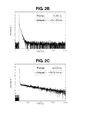
- the delayed fluorescence compounds (Coml, Com2, Com9 and Com10) of the present invention show the delayed fluorescent emission of hundreds to hundreds of thousands nano-seconds (ns).
- the delayed fluorescence compound of the present invention is activated by the field such that the excitons in the singlet state “S 1 " and the triplet state “T 1 " are transited into the intermediated state "I 1 ".
- both the exciton in the singlet state "S 1 " and the exciton in the triplet state “T 1 " are engaged in the emission.
- the FADF compound is a single molecule compound having the electron donor moiety and the electron acceptor moiety in the single molecule such that the charge transfer is easily generated. In the FADF compound with particular conditions, the charge can be separated from the electron donor moiety to the electron acceptor moiety.
- the FADF compound is activated by outer factors. It can be verified by comparing the absorption peak and the emission peak of the solution of the compounds.
- ⁇ is the Stock-shift value
- h is Planck's constant
- c is the velocity of light
- a is the onsager cavity radius
- ⁇ is a difference between the dipole moment of the excited state and the dipole moment of the ground state.
- ⁇ f is a value indicating the orientational polarizability of the solvent and may be a function of the dielectric constant of the solvent ( ⁇ ) and the refractive index of the solvent (n).
- ⁇ f ⁇ - 1 2 ⁇ + 1 - n 2 - 1 2 n 2 + 1
- the FADF can be verified by comparing the absorption peak and the emission peak of the solution of the compounds.
- the orientational polarizability ( ⁇ f) of the mixed solvent can be calculated by using the orientational polarizability of each pure solvent and their mole fraction.
- ⁇ f and ⁇ are linearly plotted by using above “Lippert-Mataga equation”
- the compound may provide the FADF emission.
- the 25% excitons in the singlet state and the 75% excitons in the triplet state are transited into the intermediate state by an outer force, i.e., a field generated when the OLED is driven.
- the excitons in the intermediate state are transited into the ground state such that the emitting efficiency is improved. Namely, in the fluorescent compound, since the singlet exciton and the triplet exciton are engaged in the emission, the emitting efficiency is improved.
- An ITO layer is deposited on a substrate and washed to form an anode (3mm*3mm).
- the substrate is loaded in a vacuum chamber, and a hole injecting layer (40 ⁇ , NPB(N,N'-di(naphthalen-1-yl)-N,N'-diphenyl-benzidine)), a hole transporting layer (10 ⁇ , mCP(N,N'-Dicarbazolyl-3,5-benzene)), an emitting material layer (200 ⁇ , host (bis ⁇ 2-[di(phenyl)phosphino]phenyl ⁇ ether oxide) and dopant (12%)), an electron transporting layer (300 ⁇ , 1,3,5-tri(phenyl-2-benzimidazole)-benzene), an electron injecting layer (10 ⁇ , LiF), and a cathode (Al) are sequentially formed on the anode under a base pressure of about 10 -6 to 10 -7 Torr.
- a hole injecting layer 40 ⁇ , NPB(N,
- the reference compound in Formula 6 is used as the dopant to form the OLED.
- the compound 1 is used as the dopant to form the OLED.
- the compound 2 is used as the dopant to form the OLED.
- the compound 3 is used as the dopant to form the OLED.
- the compound 6 is used as the dopant to form the OLED.
- the compound 7 is used as the dopant to form the OLED.
- the compound 9 is used as the dopant to form the OLED.
- the compound 10 is used as the dopant to form the OLED.
- the compound 11 is used as the dopant to form the OLED.
- Table 4 Voltage (V) Cd/A lm/W EQE (%) CIE (X) CIE (Y) Ref 7.94 4.84 1.91 2.99 0.182 0.169 Ex1 6.14 12.85 6.57 7.27 0.165 0.116 Ex2 5.92 12.45 6.60 6.92 0.168 0.111 Ex3 5.66 10.19 5.66 6.43 0.173 0.122 Ex4 5.95 10.72 5.66 5.18 0.167 0.121 Ex5 5.62 10.22 5.71 6.42 0.156 0.138 Ex6 5.25 11.76 7.03 6.99 0.169 0.104 Ex7 5.86 12.54 6.71 6.95 0.164 0.113 Ex8 5.68 10.00 5.53 6.33 0.178 0.161
- FIG. 3 is a schematic cross-sectional view of an OLED according to the invention.
- the OLED “E” is formed on a substrate (not shown).
- the OLED “E” includes a first electrode 110 as an anode, a second electrode 130 as a cathode and an organic emitting layer 120 therebetween.
- an encapsulation film which includes at least one inorganic layer and at least one organic layer and covers the OLED "E", and a cover window on the encapsulation film may be further formed to form a display device including the OLED "E".
- the substrate, the encapsulation film and the cover window may have a flexible property such that a flexible display device may be provided.
- the first electrode 110 is formed of a material having a relatively high work function
- the second electrode 130 is formed of a material having a relatively low work function.
- the first electrode 110 may be formed of indium-tin-oxide (ITO)
- the second electrode 130 may be formed of aluminum (Al) or A1 alloy (AlNd).
- the organic emitting layer 120 may include red, green and blue emitting patterns.
- the organic emitting layer 120 may have a single-layered structure.
- the organic emitting layer 120 includes a hole injection layer (HIL) 121, a hole transporting layer (HTL) 122, an emitting material layer (EML) 123, an electron transporting layer (ETL) 124 and an electron injection layer (EIL) 125 sequentially stacked on the first electrode 110.
- HIL hole injection layer
- HTL hole transporting layer
- EML electron transporting layer
- EIL electron injection layer
- At least one selected from the HIL 121, the HTL 122, the EML 123, the ETL 124 and the EIL 125 includes the delayed fluorescence compound in the Formula 1.
- the EML 123 may include the delayed fluorescence compound in the Formula 1.
- the delayed fluorescence compound acts as the dopant, and the EML 123 may further include a host to emit the blue light.
- the dopant has about 1 to 30 weight % with respect to the host.
- a difference between the HOMO of the host "HOMO Host” and the HOMO of the dopant "HOMO Dopant " or a difference between the LUMO of the host "LUMO Host " and the LUMO of the dopant "LUMO Dopant " is less than 0.5 eV. (
- the host which meets the above condition, may be selected from materials in Formula 7.
- materials in Formula 7. Bis[2-(diphenylphosphino)phenyl]ether oxide (DPEPO), 2,8-bis(diphenylphosphoryl)dibenzothiophene (PPT), 2,8-di(9H-carbazol-9-yl)dibenzothiophene (DCzDBT), m-bis(carbazol-9-yl)biphenyl (m-CBP), Diphenyl-4-triphenylsilylphenyl-phosphine oxide (TPSO1), 9-(9-phenyl-9H-carbazol-6-yl)-9H-carbazole (CCP) in an order)
- DPEPO 2,8-bis(diphenylphosphoryl)dibenzothiophene
- DCzDBT 2,8-di(9H-carbazol-9-yl)dibenzothiophene
- m-CBP m-bis(
- the triplet energy of the dopant is smaller than the triplet energy of the host, and a difference between the singlet energy of the dopant and the triplet energy of the dopant is less than 0.3eV. ( ⁇ E ST ⁇ 0.3eV) As the difference " ⁇ E ST " is smaller, the emitting efficiency is higher. In the delayed fluorescence compound of the present invention, even if the difference " ⁇ E ST " between the singlet energy of the dopant and the triplet energy of the dopant is about 0.3eV, which is relatively large, the excitons in the singlet state "S1" and the excitons in the triplet state "T1" can be transited into the intermediate state "I1".
- the delayed fluorescence compound of the present invention may act as a host in the EML 123, and the EML 123 may further include a dopant to emit the blue light.
- the dopant has about 1 to 30 weight % with respect to the host. Since the development of the blue host having excellent properties is insufficient, the delayed fluorescence compound of the present invention may be used as the host to increase the degree of freedom for the host. In this instance, the triplet energy of the dopant may be smaller than the triplet energy of the host of the delayed fluorescence compound of the present invention.
- the EML 123 may include a first dopant of the delayed fluorescence compound of the present invention, a host and a second dopant.
- the weight % summation of the first and second dopants may be about 1 to 30 to emit the blue light. In this instance, the emitting efficiency and the color purity may be further improved.
- the triplet energy of the first dopant i.e., the delayed fluorescence compound of the present invention
- the triplet energy of the first dopant may be smaller than the triplet energy of the host and larger than the triplet energy of the second dopant.
- a difference between the singlet energy of the first dopant and the triplet energy of the first dopant is less than 0.3eV. ( ⁇ E ST ⁇ 0.3eV) As the difference " ⁇ E ST " is smaller, the emitting efficiency is higher.
- the excitons in the singlet state "S 1 " and the excitons in the triplet state “T 1 " can be transited into the intermediate state "I 1 ".
- the delayed fluorescence compound of the present invention includes the first and second electron donor moieties and the electron acceptor, the charge transfer in the molecule is easily generated such that the emitting efficiency of the compound is improved.
- the dipole from the first and second electron donor moieties to the electron acceptor moiety is generated such that the dipole moment in the molecule is increased.
- the emitting efficiency is further improved.
- the excitons in the triplet state are engaged in the emission such that the emitting efficiency of the delayed fluorescent compound is increased.
- the OLED and the display device using or including the delayed fluorescence compound of the present invention has an advantage in the emitting efficiency.
Abstract
Description
- This application claims priority to and the benefit of
Korean Patent Application Nos. 10-2014-0140972 10-2014-0140973 10-2015-0130520 10-2015-0130917 - The embodiments of the invention relate to an organic light emitting diode (OLED) and more particularly to a delayed fluorescence compound having excellent emitting efficiency and an OLED and a display device using the delayed fluorescence compound.
- The requirements of the large-size display device have led to developments in flat panel display devices as an image displaying device. Among the flat panel display devices, the OLED is rapidly developed.
- In the OLED, when the electron and the hole from a cathode, which serves as an electron-injecting electrode, and an anode, which serves as a hole-injecting electrode, are injected into an emitting material layer, the electron and the hole are combined and become extinct such that the light is emitted from the OLED. A flexible substrate, for example, a plastic substrate, can be used as a base substrate for the OLED, and the OLED has excellent characteristics of driving voltage, power consumption and color purity.
- The OLED includes a first electrode as an anode on a substrate, a second electrode as a cathode facing the first electrode and an organic emitting layer therebetween.
- To improve the emitting efficiency, the organic emitting layer may include a hole injection layer (HIL), a hole transporting layer (HTL), an emitting material layer (EML), an electron transporting layer (HTL) and an electron injection layer (EIL) sequentially stacked on the first electrode.
- The hole is transferred into the EML from the first electrode through the HIL and the HTL, and the electron is transferred into the EML from the second electrode through the EIL and the ETL.
- The electron and the hole are combined in the EML to generated excitons, and the excitons are transited from an excited state to a ground state such the light is emitted.
- The External quantum efficiency () of the emitting material for the EML can be expressed by:

- In the above equation, "ηint" is the internal quantum efficiency, "Γ " is the charge balance factor, "Φ" is the radiative quantum efficiency, and "ηout-coupling" is the out-coupling efficiency.
- The charge balance factor "r " means a balance between the hole and the electron generating the exciton. Generally, assuming 1:1 matching of the hole and the electrode, the charge balance factor has a value of "1". The radiative quantum efficiency "Φ " is a value regarding an effective emitting efficiency of the emitting material. In the host-dopant system, the radiative quantum efficiency depends on a fluorescent quantum efficiency of the dopant.
- The internal quantum efficiency "ηint" is a ratio of the excitons generating the light to the excitons generated by the combination of the hole and the electron. In the fluorescent compound, a maximum value of the internal quantum efficiency is 0.25. When the hole and the electron are combined to generate the exciton, a ratio of the singlet excitons to the triplet excitons is 1:3 according to the spin structure. However, in the fluorescent compound, only the singlet excitons excluding the triplet excitons are engaged in the emission.
- The out-coupling efficiency "ηout-coupling" is a ratio of the light emitted from the display device to the light emitted from the EML. When the isotropic compounds are deposited in a thermal evaporation method to form a thin film, the emitting materials are randomly oriented. In this instance, the out-coupling efficiency of the display device may be assumed as 0.2.
- Accordingly, the maximum emitting efficiency of the OLED including the fluorescent compound as the emitting material is less than about 5%.
- To overcome the disadvantage of the emitting efficiency of the fluorescent compound, the phosphorescent compound, where both the singlet excitons and the triplet excitons are engaged in the emission, has been developed for the OLED.
- The red and green phosphorescent compound having a relatively high efficiency are introduced and developed. However, there is no blue phosphorescent compound meeting the requirements in the emitting efficiency and the reliability.
- Accordingly, the embodiment of the invention is directed to a delayed fluorescence compound and an OLED and a display device using the same that substantially obviate one or more of the problems due to limitations and disadvantages of the related art.
- An object of the embodiment of the invention is to provide a delayed fluorescence compound having high emitting efficiency.
- Another object of the embodiment of the invention is to provide an OLED and a display device having an improved emission efficiency.
- Additional features and advantages of the invention will be set forth in the description which follows, and in part will be apparent from the description, or may be learned by practice of the invention. The objectives and other advantages of the invention will be realized and attained by the structure particularly pointed out in the written description and claims hereof as well as the appended drawings.
- To achieve these and other advantages and in accordance with the purpose of the embodiments of the invention, as embodied and broadly described herein, an aspect of an embodiment of the invention provides a delayed fluorescence compound including a first electron donor moiety of indolo-[3,2,1-j,k]carbazole; a second electron donor moiety selected from indolo-[3,2,1-j,k]carbazole, carbazole or triphenylamine; and an electron acceptor moiety selected from dibenzothiophene sulfone or diphenyl sulfone, wherein the first and second electron donor moieties are combined to the electron acceptor moiety, and the electron acceptor moiety is combined to a first position or a para-position of the first electron donor moiety.
- In another aspect of the embodiment of the invention, provided is a delayed fluorescence compound of Formula 1:


- In another aspect of the embodiment of the invention provided is an organic light emitting diode including a first electrode; a second electrode facing the first electrode; and an organic emitting layer between the first and second electrodes and including a delayed fluorescence compound, wherein the delayed fluorescence compound includes a first electron donor moiety of indolo-[3,2,1-j,k]carbazole, a second electron donor moiety selected from indolo-[3,2,1-j,k]carbazole, carbazole or triphenylamine, and an electron acceptor moiety selected from dibenzothiophene sulfone or diphenyl sulfone, wherein the first and second electron donor moieties are combined to the electron acceptor moiety, and the electron acceptor moiety is combined to a first position or a para-position of the first electron donor moiety.
- In another aspect of the embodiment of the invention provided is an organic light emitting diode including a first electrode; a second electrode facing the first electrode; and an organic emitting layer between the first and second electrodes and including a delayed fluorescence compound of Formula 1:


- In another aspect of the embodiment of the invention provided is a display device including a substrate; an organic light emitting diode on the substrate and including a first electrode, a second electrode facing the first electrode and an organic emitting layer between the first and second electrodes and including a delayed fluorescence compound; an encapsulation film on the organic light emitting diode; and a cover window on the encapsulation film, wherein the delayed fluorescence compound includes a first electron donor moiety of indolo-[3,2,1-j,k]carbazole, a second electron donor moiety selected from indolo-[3,2,1-j,k]carbazole, carbazole or triphenylamine, and an electron acceptor moiety selected from dibenzothiophene sulfone or diphenyl sulfone, wherein the first and second electron donor moieties are combined to the electron acceptor moiety, and the electron acceptor moiety is combined to a first position or a para-position of the first electron donor moiety.
- In another aspect of the embodiment of the invention provided is a display device including a substrate; an organic light emitting diode on the substrate and including a first electrode, a second electrode facing the first electrode and an organic emitting layer between the first and second electrodes and including a delayed fluorescence compound of Formula 1:


- It is to be understood that both the foregoing general description and the following detailed description are by example and explanatory and are intended to provide further explanation of the invention as claimed.
- The accompanying drawings, which are included to provide a further understanding of the invention and are incorporated in and constitute a part of this specification, illustrate embodiments of the invention and together with the description serve to explain the principles of the invention.
-
FIG. 1 is a view illustrating an emission mechanism of a delayed fluorescence compound according to the present invention. -
FIGs. 2A to 2D respectively show distribution of HOMO and LUMO ofcompound 1 of the present invention. -
FIG. 3 is a schematic cross-sectional view of an OLED according to the invention. - The meanings of terms described in the present specification should be understood as follows.
- The singular forms should be understood as including the plural forms as well unless the context clearly indicates otherwise. The terms "first", "second", and the like are used to discriminate any one element from other elements and the scope of the present invention is not intended to be limited by these terms. The terms "comprises" "includes" and the like should be understood as not precluding the presence or addition of one or more other features, integers, steps, operations, elements, components, or combinations thereof. The term "at least one" should be understood as including all combinations that may be suggested from one or more associated items. For example, the meanings of "at least one selected from a first item, a second item, and a third item" includes not only each of the first item, the second item, and the third item, but also all combinations of these items that may be suggested from two or more ones of the first item, the second item, and the third item. In addition, when any one element is referred to as being "on" another element, it can be directly on the upper surface of the other element or a third intervening element may also be present.
- Reference will now be made in detail to example embodiments, examples of which are illustrated in the accompanying drawings.
- A delayed fluorescence compound of the present invention has a structure in that a first electron donor moiety of indolo-[3,2,1-j,k]carbazole and a second electron donor moiety are respectively combined (or linked) to an electron acceptor moiety and the electron acceptor moiety is combined to a third or para- positions of the first electron donor moiety. The delayed fluorescent compound of the present invention has
Formula 1 of following.

- In the
Formula 1, one of "m" and "n" is 1, and the other one of "m" and "n" is 0 (zero). Namely, the delayed fluorescent compound in the Formula 1 may have Formula 2-1 or Formula 2-2 followings:

- In other words, as shown in the Formula 2-1, the delayed fluorescence compound of the present invention may have a structure in that a first electron donor moiety of indolo-[3,2,1-j,k]carbazole and a second electron donor moiety are respectively combined (or linked) to an electron acceptor moiety and the electron acceptor moiety is combined to a third position of the first electron donor moiety.
- Alternatively, as shown in the Formula 2-2, the delayed fluorescence compound of the present invention may have a structure in that a first electron donor moiety of indolo-[3,2,1-j,k]carbazole and a second electron donor moiety are respectively combined (or linked) to an electron acceptor moiety and the electron acceptor moiety is combined to a para- position of the first electron donor moiety.
- In the
Formulas 1, 2-1 and 2-2, each of Y1 and Y2 as the second electron donor moiety is independently selected from indolo-[3,2,1-j,k]carbazole, carbazole or triphenylamine. The first and second electron donor moieties are same or different. For example, each of Y1 and Y2 as the second electron donor moiety is independently selected from materials in Formula 3 of following:
- In the
Formulas 1, 2-1 and 2-2, each of X1 and X2 as the electron acceptor moiety is independently selected from dibenzothiophene sulfone or diphenyl sulfone. For example, each of X1 and X2 as the second electron acceptor moiety is independently selected from materials in Formula 4 of following:
- Since the delayed fluorescence compound includes the first and second electron donor moieties and the electron acceptor moiety, the charge transfer is easily generated in the molecule and the emitting efficiency is improved. In addition, the dipole from the first and second electron donor moieties to the electron acceptor moiety is generated such that the dipole moment in the molecule is increased. As a result, the emitting efficiency is further improved.
- Moreover, in the delayed fluorescent compound of the present invention, the excitons in the triplet state are engaged in the emission such that the emitting efficiency of the delayed fluorescent compound is increased.
- Further, since indolo-[3,2,1-j,k]carbazole, which has high triplet energy and excellent hole property, is used for the first electron donor moiety and optionally for the second electron donor moiety, the increase of the emitting efficiency is further increased. (HOMO : - 5.56eV, LUMO : - 1.25eV, ET = 3.04 eV)
- Since the delayed fluorescence compound of the present invention has a rigid structure due to indolo-[3,2,1-j,k]carbazole such that the vibration in the molecule is decreased. As a result, the color shift problem is decreased, and the color purity is improved. In addition, since the delayed fluorescence compound of the present invention has large molecular weight, the thermal stability is increased.
- In the delayed fluorescence compound of the present invention, the first and second electron donor moieties and the electron acceptor moiety are combined or linked in the molecule such that an overlap between highest occupied molecular orbital (HOMO) and lowest unoccupied molecular orbital (LUMO) is reduced. As a result, a field activated complex is generated, and the emitting efficiency of the delayed fluorescence compound is improved.
- Referring to
FIG. 1 , which is a view illustrating an emission mechanism of a delayed fluorescence compound according to the present invention, in the delayed fluorescence compound of the present invention, the triplet excitons as well as the singlet excitons are engaged in the emission such that the emitting efficiency is improved. - Namely, the triplet exciton is activated by a field, and the triplet exciton and the singlet exciton are transferred into an intermediated state "I1" and transited into a ground state "So" to emit the light. In other words, the singlet state "S1" and the triplet state "T1" are transited into the intermediated state "I1" (S1-> I1 <-T1), and the singlet exciton and the triplet exciton in the intermediated state "I1" are engaged in the emission such that the emitting efficiency is improved. The compound having the above emission mechanism may be referred to as a field activated delayed fluorescence (FADF) compound.
- In the related art fluorescence compound, since the HOMO and the LUMO are dispersed throughout an entirety of the molecule, the interconversion of the HOMO and the LUMO is impossible. (Selection Rule)
- However, in the FADF compound, since the overlap between the HOMO and the LUMO in the molecule is relatively small, the interaction between the HOMO and the LUMO is small. Accordingly, changes of the spin state of one electron do not affect other electrons, and new charge transfer band, which does not comply the Selection Rule, is generated.
- Moreover, since the electron donor moiety and the electron acceptor moiety is spatially spaced apart from each other in the molecule, the dipole moment is generated in a polarized state. In the polarized state dipole moment, the interaction between the HOMO and the LUMO is further reduced such that the emission mechanism does not comply the Selection Rule. Accordingly, in the FADF compound, the transition from the triplet state "T1" and the singlet state "S1" into the intermediated state "I1" can be generated such that the triplet exciton can be engaged in the emission.
- When the OLED is driven, the intersystem transition (intersystem crossing) from 25% singlet state "S1" excitons and 75% triplet state "T1" excitons to the intermediated state "I1" is generated, and the singlet and triplet excitons in the intermediated state "I1" are transited into the ground state to emit the light. As a result, the FADF compound has the theoretic quantum efficiency of 100%.
- For example, the delayed fluorescence compound in the
Formula 1 may be one of compounds in Formula 5. (Compounds 1 to 12 in an order)

- The HOMO, the LUMO and the energy band gap of the
compounds 1 to 12 are listed in Table 1.Table 1 HOMO (eV) LUMO (eV) Band gap Compound 1 -5.58 -1.67 3.91 Compound 2 -5.65 -1.62 4.03 Compound 3 -5.94 -1.96 3.98 Compound 4 -5.70 -1.83 3.87 Compound 5 -5.12 -1.59 3.53 Compound 6 -5.17 -1.80 3.37 Compound 7 -5.68 -1.52 4.16 Compound 8 -5.67 -1.59 4.08 Compound 9 -5.62 -1.91 3.71 Compound 10 -5.70 -1.73 3.97 Compound 11 -5.10 -1.51 3.59 Compound 12 -5.16 -1.74 3.42 - As shown in Table 1, the delayed fluorescence compound of the present invention has large energy band gap such that the emitting efficiency of an OLED or a display device including the compound may be increased.
-

- In the N2 gas purging system, compound A, compound B (2 equivalent), potassium carbonate (2 equivalent) and copper (Cu) were put into diethylene glycol, and the mixture was stirred. After stirring for about 1 hour under a temperature of 240 °C, the reaction was completed. The mixture was extracted by boiled acetone to remove the organic solvent. The resultant was put into the diluted hydrochloric acid solution. After washing by DI water, the resultant was re-crystallized by using acetone and methanol such that compound C was obtained.
-

- In the N2 gas purging system, compound C was put into acetic acid, and the mixture was stirred under a temperature of 70 °C. Activated zinc, which was activated with diluted hydrochloric acid, was added, and the mixture was refluxed for 1 hour after the color of the mixture was changed. After completion of the reflux, the mixture was cooled into the room temperature, and DI water was added to obtain solids. The solids were filtered to remove zinc, and the residuals were put into acetic acid. Diluted hydrochloric acid by DI water (hydrochloric acid : DI water=1: 10 (vol.%)) of excess amount was added into the mixture to obtain solids. The solids was washed by DI water such that compound D was obtained.
-

- In the ice bath, compound D was put into acetic acid, and sulfuric acid was added and stirred. Sodium nitride (1.1 equivalent) was dissolved in DI water, and the solution was slowly added into the flask including the compound D for 15 minutes and was additionally stirred for 10 minutes. The flask was transferred into the oil bath, and the mixture was reacted for 20 minutes under a temperature of 130 °C. After completion of the reaction, the mixture was cooled into the room temperature, and DI water was put into the resultant to obtain the precipitates. The precipitates was filtered and washed by methanol. The filtered precipitated was columned and re-crystallized by using dichloromethane and methanol such that compound E was obtained.
-


- In the N2 gas purging system, compound E, bis(pinacolate)diboron (1.2 equivalent), [1,1-bis(diphenylphosphineo)ferrocene]palladium(II), dichloride dichloromethane, 1,1-bis(diphenylphosphino)ferrocene and potassium acetate were put into the mixed solvent of 1,4-dioxane and toluene (1:1) in the flask, where the light was blocked out, and stirred. After the bubbles were disappeared, the mixture was stirred for 17 hours under a temperature of 120°C in the oil bath. After completion of the reaction, the mixture was cooled into the room temperature, and the solvent was removed. The resultant was washed by dichloromethane and refined such that compound F was obtained.
-

- In the N2 gas purging system, compound G was put into acetic acid and was stirred. 30% hydrogen peroxide was excessively added. The mixture was refluxed for 8 hours under a temperature of 110°C, and the reaction was completed. The mixture was cooled into the room temperature, and water was added to be precipitate. The mixture was stirred for about 30 minutes, and the precipitate was filtered. The resultant was washed by water such that compound H was obtained.
-

- In the N2 gas purging system, compound A (1 equivalent) was dissolved in 1,4-dioxane, and CuI and K3PO4 were added. Compound H (1.1 equivalent) and trans-1,2-diaminocyclohexane were added into the flask including the compound A. The mixture was stirred and refluxed for 24 hours under a temperature of 110°C. After completion of the reaction, the mixture, which was cooled into the room temperature, was extracted by using water and ethyl acetate. The resultant was columned by using the solvent of ethyl acetate and hexane such that compound I was obtained.
-

- In the N2 gas purging system, compound I was dissolved in toluene, and compound F (1.2 equivalent) was added. K2CO3 (4.4 equivalent), which was dissolved in DI water, was added into the mixture. After adding tetrahydrofuran, and Pd (0.05 equivalent) was added. The mixture was refluxed and stirred under a temperature of 80 °C. The mixture was extracted and was re-crystallized for separation of compound I, compound F and the by-products. The resultant was columned by dichloromethane and hexane such that
compound 1 was obtained. -

- In the N2 gas purging system, compound H was dissolved in toluene, and compound F (2.4 equivalent) was added. K2CO3 (8.8 equivalent), which was dissolved in DI water, was added into the mixture. After adding tetrahydrofuran, and Pd (0.1 equivalent) was added. The mixture was refluxed and stirred under a temperature of 80 °C. The mixture was extracted and was re-crystallized for separation of compound H, compound F and the by-products. The resultant was columned by dichloromethane and hexane such that compound 2 was obtained.
-

- In the N2 gas purging system, compound G-1 was put into acetic acid and was stirred. 30% hydrogen peroxide was excessively added. The mixture was refluxed for 8 hours under a temperature of 110°C, and the reaction was completed. The mixture was cooled into the room temperature, and water was slowly added to be precipitate. The mixture was additionally stirred for about 30 minutes, and the precipitate was filtered. The resultant was washed by water such that compound H-1 was obtained.
-

- In the N2 gas purging system, compound A (1 equivalent) was dissolved in 1,4-dioxane, and CuI and K3PO4 were added. Compound H-1 (1.1 equivalent) and trans-1,2-diaminocyclohexane were added into the flask including the compound A. The mixture was stirred and refluxed for 24 hours under a temperature of 110°C. After completion of the reaction, the mixture, which was cooled into the room temperature, was extracted by using water and ethyl acetate. The resultant was columned by using the solvent of ethyl acetate and hexane such that compound I-1 was obtained.
-

- In the N2 gas purging system, compound I-1 was dissolved in toluene, and compound F (1.2 equivalent) was added. K2CO3 (4.4 equivalent), which was dissolved in DI water, was added into the mixture. After adding tetrahydrofuran, and Pd (0.05 equivalent) was added. The mixture was refluxed and stirred for 8 hours under a temperature of 80 °C. The mixture was extracted and was re-crystallized for separation of compound I-1, compound F and the by-products. The resultant was columned by dichloromethane and hexane such that compound 3 was obtained.
-

- In the N2 gas purging system, compound H-1 was dissolved in toluene, and compound F (2.4 equivalent) was added. K2CO3 (8.8 equivalent), which was dissolved in DI water, was added into the mixture. After adding tetrahydrofuran, and Pd (0.1 equivalent) was added. The mixture was refluxed and stirred for 8 hours under a temperature of 80 °C. The mixture was extracted and was re-crystallized for separation of compound H-1, compound F and the by-products. The resultant was columned by dichloromethane and hexane such that compound 4 was obtained.
-

- In the N2 gas purging system, compound J was dissolved in tetrahydrofuran, and n-butyl-lithium (1.2 equivalent) was slowly added under a temperature of -78°C. The mixture was stirred for 1 hour under a temperature of -78 °C. After additionally stirring the mixture for 2 hours under the room temperature, the mixture was cooled into a temperature of -78°C, and trimethyl-borate was added. The temperature of the mixture was slowly increased into the room temperature and was stirred for 2 hours. Diluted hydrochloric acid (5.0%) was added into the mixture and stirred for 1 hour under a condition of pH 5 to 6. The solution was extracted by methylene chloride. The organic part was extracted by brine and DI water, and moisture was removed by MgSO4. The organic solvent was removed such that compound K was obtained.
-

- In the N2 gas purging system, compound H was dissolved in toluene, and compound K (1.1 equivalent) was added. K2CO3 (4.4 equivalent), which was dissolved in DI water, was added into the mixture. After adding tetrahydrofuran, and Pd (0.05 equivalent) was added. The mixture was refluxed and stirred under a temperature of 80 °C. The mixture was extracted and was re-crystallized for separation of compound H, compound K and the by-products. The resultant was columned by dichloromethane and hexane such that compound L was obtained.
-


- In the N2 gas purging system, compound L was dissolved in toluene, and compound F (1.1 equivalent) was added. K2CO3 (4.4 equivalent), which was dissolved in DI water, was added into the mixture. After adding tetrahydrofuran, and Pd (0.05 equivalent) was added. The mixture was refluxed and stirred under a temperature of 80 °C. The mixture was extracted and was re-crystallized for separation of compound L, compound F and the by-products. The resultant was columned by dichloromethane and hexane such that compound 5 was obtained.
-

- In the N2 gas purging system, compound H-1 was dissolved in toluene, and compound K (1.1 equivalent) was added. K2CO3 (4.4 equivalent), which was dissolved in DI water, was added into the mixture. After adding tetrahydrofuran, and Pd (0.05 equivalent) was added. The mixture was refluxed and stirred under a temperature of 80°C. The mixture was extracted and was re-crystallized for separation of compound H-1, compound K and the by-products. The resultant was columned by dichloromethane and hexane such that compound L-1 was obtained.
-

- In the N2 gas purging system, compound L-1 was dissolved in toluene, and compound F (1.1 equivalent) was added. K2CO3 (4.4 equivalent), which was dissolved in DI water, was added into the mixture. After adding tetrahydrofuran, and Pd (0.05 equivalent) was added. The mixture was refluxed and stirred under a temperature of 80 °C. The mixture was extracted and was re-crystallized for separation of compound L-1, compound F and the by-products. The resultant was columned by dichloromethane and hexane such that compound 6 was obtained.
-


- In the N2 gas purging system, compound A, compound B (1.1 equivalent) and cesium carbonate (1.5 equivalent) were put into dimethylsulfoxide, and the mixture was stirred. After stirring for about 2 hour under the room temperature, the mixture was put into and stirred under a temperature of 60 °C in the oil bath. 8 hours after, the mixture was put into iced DI water such that yellow solids were obtained. The yellow solids were filtered and extracted by using dichloromethane and DI water. Moisture was removed by MgSO4, and the organic solvent was removed. The resultant was re-crystallized by using dichloromethane and methanol such that compound C was obtained.
-

- In the N2 gas purging system, compound C and SnCl2·2H2O were put into ethanol, and the mixture was stirred for 8 hours under a temperature of 70 °C. After completion of the reaction, the mixture was cooled into the room temperature. The mixture was added into IN sodium hydroxide aqueous solution to obtain solids. The solids were filtered and dissolved in dichloromethane. IN sodium hydroxide aqueous solution was added to be extracted. The aqueous layer was removed to obtain an organic layer. The organic layer was extracted by DI water, and moisture was removed by MgSO4. The organic solvent was removed such that compound D was obtained.
-

- In the ice bath, compound D was put into acetic acid, and sulfuric acid was added and stirred. Sodium nitride (1.1 equivalent) was dissolved in DI water, and the solution was slowly added into the flask including the compound D for 15 minutes and was additionally stirred for 10 minutes. The flask was transferred into the oil bath, and the mixture was reacted for 20 minutes under a temperature of 130 °C. After completion of the reaction, the mixture was cooled into the room temperature, and DI water was put into the resultant to obtain the precipitates. The precipitates was filtered and washed by methanol. The filtered precipitated was columned and re-crystallized by using dichloromethane and methanol such that compound E was obtained.
-

- In the N2 gas purging system, compound E and N-bromosuccinimide was put into dichloromethane in the flask, where the light was blocked out, and the mixture was stirred for 12 hours. After completion of the reaction, the mixture was extracted by using dichloromethane and DI water, and moisture was removed by MgSO4. The resultant was refined such that compound F was obtained.
-

- In the N2 gas purging system, compound F, bis(pinacolate)diboron (1.2 equivalent), [1,1-bis(diphenylphosphineo)ferrocene]palladium(II), dichloride dichloromethane, 1,1-bis(diphenylphosphino)ferrocene and potassium acetate were put into the mixed solvent of 1,4-dioxane and toluene (1:1) in the flask, where the light was blocked out, and stirred. After the bubbles were disappeared, the mixture was stirred for 17 hours under a temperature of 120°C in the oil bath. After completion of the reaction, the mixture was cooled into the room temperature, and the solvent was removed. The resultant was washed by dichloromethane and refined such that compound G was obtained.
-


- In the N2 gas purging system, compound H was put into acetic acid and was stirred. 30% hydrogen peroxide was excessively added. The mixture was refluxed for 8 hours under a temperature of 110°C, and the reaction was completed. The mixture was cooled into the room temperature, and water was added to be precipitate. The mixture was stirred for about 30 minutes, and the precipitate was filtered. The resultant was washed by water such that compound I was obtained.
-

- In the N2 gas purging system, compound A (1 equivalent) was dissolved in 1,4-dioxane, and CuI and K3PO4 were added. Compound I (1.1 equivalent) and trans-1,2-diaminocyclohexane were added into the flask including the compound A. The mixture was stirred and refluxed for 24 hours under a temperature of 110°C. After completion of the reaction, the mixture, which was cooled into the room temperature, was extracted by using water and ethyl acetate. The resultant was columned by using the solvent of ethyl acetate and hexane such that compound J was obtained.
- (8) compound 7

- In the N2 gas purging system, compound J was dissolved in toluene, and compound G (1.2 equivalent) was added. K2CO3 (4.4 equivalent), which was dissolved in DI water, was added into the mixture. After adding tetrahydrofuran, and Pd (0.05 equivalent) was added. The mixture was refluxed and stirred under a temperature of 80 °C. The mixture was extracted and was re-crystallized for separation of compound J, compound G and the by-products. The resultant was columned by dichloromethane and hexane such that compound 7 was obtained.
-


- In the N2 gas purging system, compound I was dissolved in toluene, and compound G (2.4 equivalent) was added. K2CO3 (8.8 equivalent), which was dissolved in DI water, was added into the mixture. After adding tetrahydrofuran, and Pd (0.1 equivalent) was added. The mixture was refluxed and stirred under a temperature of 80 °C. The mixture was extracted and was re-crystallized for separation of compound I, compound G and the by-products. The resultant was columned by dichloromethane and hexane such that compound 8 was obtained.
-

- In the N2 gas purging system, compound H-1 was put into acetic acid and was stirred. 30% hydrogen peroxide was excessively added. The mixture was refluxed for 8 hours under a temperature of 110°C, and the reaction was completed. The mixture was cooled into the room temperature, and water was slowly added to be precipitate. The mixture was additionally stirred for about 30 minutes, and the precipitate was filtered. The resultant was washed by water such that compound I-1 was obtained.
-

- In the N2 gas purging system, compound A (1 equivalent) was dissolved in 1,4-dioxane, and CuI and K3PO4 were added. Compound I-1 (1.1 equivalent) and trans-1,2-diaminocyclohexane were added into the flask including the compound A. The mixture was stirred and refluxed for 24 hours under a temperature of 110°C. After completion of the reaction, the mixture, which was cooled into the room temperature, was extracted by using water and ethyl acetate. The resultant was columned by using the solvent of ethyl acetate and hexane such that compound J-1 was obtained.
-


- In the N2 gas purging system, compound J-1 was dissolved in toluene, and compound G (1.2 equivalent) was added. K2CO3 (4.4 equivalent), which was dissolved in DI water, was added into the mixture. After adding tetrahydrofuran, and Pd (0.05 equivalent) was added. The mixture was refluxed and stirred for 8 hours under a temperature of 80 °C. The mixture was extracted and was re-crystallized for separation of compound J-1, compound G and the by-products. The resultant was columned by dichloromethane and hexane such that compound 9 was obtained.
-

- In the N2 gas purging system, compound I-1 was dissolved in toluene, and compound G (2.4 equivalent) was added. K2CO3 (8.8 equivalent), which was dissolved in DI water, was added into the mixture. After adding tetrahydrofuran, and Pd (0.1 equivalent) was added. The mixture was refluxed and stirred for 8 hours under a temperature of 80°C. The mixture was extracted and was re-crystallized for separation of compound I-1, compound G and the by-products. The resultant was columned by dichloromethane and hexane such that compound 10 was obtained.
-

- In the N2 gas purging system, compound K was dissolved in tetrahydrofuran, and n-butyl-lithium (1.2 equivalent) was slowly added under a temperature of -78°C. The mixture was stirred for 1 hour under a temperature of -78 °C. After additionally stirring the mixture for 2 hours under the room temperature, the mixture was cooled into a temperature of -78°C, and trimethyl-borate was added. The temperature of the mixture was slowly increased into the room temperature and was stirred for 2 hours. Diluted hydrochloric acid (5.0%) was added into the mixture and stirred for 1 hour under a condition of pH 5 to 6. The solution was extracted by methylene chloride. The organic part was extracted by brine and DI water, and moisture was removed by MgSO4. The organic solvent was removed such that compound L was obtained.
-

- In the N2 gas purging system, compound I was dissolved in toluene, and compound L (1.1 equivalent) was added. K2CO3 (4.4 equivalent), which was dissolved in DI water, was added into the mixture. After adding tetrahydrofuran, and Pd (0.05 equivalent) was added. The mixture was refluxed and stirred under a temperature of 80 °C. The mixture was extracted and was re-crystallized for separation of compound I, compound L and the by-products. The resultant was columned by dichloromethane and hexane such that compound M was obtained.
-

- In the N2 gas purging system, compound M was dissolved in toluene, and compound G (1.1 equivalent) was added. K2CO3 (4.4 equivalent), which was dissolved in DI water, was added into the mixture. After adding tetrahydrofuran, and Pd (0.05 equivalent) was added. The mixture was refluxed and stirred under a temperature of 80°C. The mixture was extracted and was re-crystallized for separation of compound M, compound G and the by-products. The resultant was columned by dichloromethane and hexane such that compound 11 was obtained.
-

- In the N2 gas purging system, compound I-1 was dissolved in toluene, and compound L (1.1 equivalent) was added. K2CO3 (4.4 equivalent), which was dissolved in DI water, was added into the mixture. After adding tetrahydrofuran, and Pd (0.05 equivalent) was added. The mixture was refluxed and stirred under a temperature of 80 °C. The mixture was extracted and was re-crystallized for separation of compound I-1, compound L and the by-products. The resultant was columned by dichloromethane and hexane such that compound M-1 was obtained.
-


- In the N2 gas purging system, compound M-1 was dissolved in toluene, and compound G (1.1 equivalent) was added. K2CO3 (4.4 equivalent), which was dissolved in DI water, was added into the mixture. After adding tetrahydrofuran, and Pd (0.05 equivalent) was added. The mixture was refluxed and stirred under a temperature of 80 °C. The mixture was extracted and was re-crystallized for separation of compound M-1, compound G and the by-products. The resultant was columned by dichloromethane and hexane such that compound 12 was obtained.
- The mass spectrum data of the
above compounds 1 to 12 are listed in Table 2.Table 2 Calculation Found (M(H+) Com1 C42H26N2O2S 622.17 623.05 Com2 C48H28N2O2S 696.19 697.47 Com3 C42H24N2O2S 620.16 620.98 Com4 C48H26N2O2S 694.17 695.28 Com5 C48H32N2O2S 700.22 701.39 Com6 C48H30N2O2S 698.20 699.05 Com7 C42H26N2O2S 622.17 622.93 Com8 C48H28N2O2S 696.19 697.31 Com9 C42H24N2O2S 620.16 621.20 Com10 C48H26N2O2S 694.17 695.08 Com11 C48H32N2O2S 700.22 701.16 Com12 C48H30N2O2S 698.20 699.49 - The emission properties of the
above compounds 1, 2, 9 and 10 (Coml, Com2, Com9 and Com10) are measured and the results are listed in Table 3 and shown inFIGs. 2A to 12D . (Quantarus tau apparatus of Hamamatsu Co., Ltd. O2 free condition)Table 3 Prompt (ns) Delayed (ns) 
17.01 4706.58 Com1 
10.44 311.20 Com2 
62.05 7273.16 Com9 
12.65 2658.03 Com10 - As shown in Table 3 and
FIGs. 2A to 2D , the delayed fluorescence compounds (Coml, Com2, Com9 and Com10) of the present invention show the delayed fluorescent emission of hundreds to hundreds of thousands nano-seconds (ns). - As mentioned above, the delayed fluorescence compound of the present invention is activated by the field such that the excitons in the singlet state "S1" and the triplet state "T1" are transited into the intermediated state "I1". As a result, both the exciton in the singlet state "S1" and the exciton in the triplet state "T1" are engaged in the emission.
- The FADF compound is a single molecule compound having the electron donor moiety and the electron acceptor moiety in the single molecule such that the charge transfer is easily generated. In the FADF compound with particular conditions, the charge can be separated from the electron donor moiety to the electron acceptor moiety.
- The FADF compound is activated by outer factors. It can be verified by comparing the absorption peak and the emission peak of the solution of the compounds.

- In the above equation, "Δυ" is the Stock-shift value, and "υ abs" and "υfl" are the wave-number of the maximum absorption peak and the maximum emission peak, respectively. "h" is Planck's constant, "c" is the velocity of light, "a" is the onsager cavity radius, and "Δµ " is a difference between the dipole moment of the excited state and the dipole moment of the ground state. (Δµ = µe - µg)
- "Δf" is a value indicating the orientational polarizability of the solvent and may be a function of the dielectric constant of the solvent (ε) and the refractive index of the solvent (n).

- Since the intensity of dipole moment in the excited state is determined by the peripheral polarity (e.g., the polarity of the solvent), the FADF can be verified by comparing the absorption peak and the emission peak of the solution of the compounds.
- The orientational polarizability (Δf) of the mixed solvent can be calculated by using the orientational polarizability of each pure solvent and their mole fraction. When "Δf" and "Δυ" are linearly plotted by using above "Lippert-Mataga equation", the compound may provide the FADF emission.
- Namely, when the FADF complex is stabilized according to the orientational polarizability of the solvent, the emission peak is shifted in a long wavelength according to the degree of the stabilization. Accordingly, when the compound provides the FADF emission, "Δf" and "Δυ" are plotted in a linear line. When "Δf" and "Δυ" are plotted in a linear line, the compound provides the FADF emission.
- In the delayed fluorescence compound of the present invention, the 25% excitons in the singlet state and the 75% excitons in the triplet state are transited into the intermediate state by an outer force, i.e., a field generated when the OLED is driven. (Intersystem crossing) The excitons in the intermediate state are transited into the ground state such that the emitting efficiency is improved. Namely, in the fluorescent compound, since the singlet exciton and the triplet exciton are engaged in the emission, the emitting efficiency is improved.
- An ITO layer is deposited on a substrate and washed to form an anode (3mm*3mm). The substrate is loaded in a vacuum chamber, and a hole injecting layer (40Å, NPB(N,N'-di(naphthalen-1-yl)-N,N'-diphenyl-benzidine)), a hole transporting layer (10Å, mCP(N,N'-Dicarbazolyl-3,5-benzene)), an emitting material layer (200Å, host (bis{2-[di(phenyl)phosphino]phenyl}ether oxide) and dopant (12%)), an electron transporting layer (300Å, 1,3,5-tri(phenyl-2-benzimidazole)-benzene), an electron injecting layer (10Å, LiF), and a cathode (Al) are sequentially formed on the anode under a base pressure of about 10-6 to 10-7 Torr.
- The reference compound in Formula 6 is used as the dopant to form the OLED.
- The
compound 1 is used as the dopant to form the OLED. - The compound 2 is used as the dopant to form the OLED.
- The compound 3 is used as the dopant to form the OLED.
- The compound 6 is used as the dopant to form the OLED.
- The compound 7 is used as the dopant to form the OLED.
- The compound 9 is used as the dopant to form the OLED.
- The compound 10 is used as the dopant to form the OLED.
- The compound 11 is used as the dopant to form the OLED.

Table 4 Voltage (V) Cd/A lm/W EQE (%) CIE (X) CIE (Y) Ref 7.94 4.84 1.91 2.99 0.182 0.169 Ex1 6.14 12.85 6.57 7.27 0.165 0.116 Ex2 5.92 12.45 6.60 6.92 0.168 0.111 Ex3 5.66 10.19 5.66 6.43 0.173 0.122 Ex4 5.95 10.72 5.66 5.18 0.167 0.121 Ex5 5.62 10.22 5.71 6.42 0.156 0.138 Ex6 5.25 11.76 7.03 6.99 0.169 0.104 Ex7 5.86 12.54 6.71 6.95 0.164 0.113 Ex8 5.68 10.00 5.53 6.33 0.178 0.161 - As shown in Table 4, in the OLEDs using the compounds of the present invention (Ex1 to Ex8), the color purity and the emitting efficiency are improved.
-
FIG. 3 is a schematic cross-sectional view of an OLED according to the invention. - As shown in
FIG. 3 , the OLED "E" is formed on a substrate (not shown). The OLED "E" includes afirst electrode 110 as an anode, asecond electrode 130 as a cathode and an organic emittinglayer 120 therebetween. - Although not shown, an encapsulation film, which includes at least one inorganic layer and at least one organic layer and covers the OLED "E", and a cover window on the encapsulation film may be further formed to form a display device including the OLED "E". The substrate, the encapsulation film and the cover window may have a flexible property such that a flexible display device may be provided.
- The
first electrode 110 is formed of a material having a relatively high work function, and thesecond electrode 130 is formed of a material having a relatively low work function. For example, thefirst electrode 110 may be formed of indium-tin-oxide (ITO), and thesecond electrode 130 may be formed of aluminum (Al) or A1 alloy (AlNd). The organic emittinglayer 120 may include red, green and blue emitting patterns. - The organic emitting
layer 120 may have a single-layered structure. Alternatively, to improve the emitting efficiency, the organic emittinglayer 120 includes a hole injection layer (HIL) 121, a hole transporting layer (HTL) 122, an emitting material layer (EML) 123, an electron transporting layer (ETL) 124 and an electron injection layer (EIL) 125 sequentially stacked on thefirst electrode 110. - At least one selected from the
HIL 121, theHTL 122, theEML 123, theETL 124 and theEIL 125 includes the delayed fluorescence compound in theFormula 1. - For example, the
EML 123 may include the delayed fluorescence compound in theFormula 1. The delayed fluorescence compound acts as the dopant, and theEML 123 may further include a host to emit the blue light. In this instance, the dopant has about 1 to 30 weight % with respect to the host. - A difference between the HOMO of the host "HOMOHost" and the HOMO of the dopant "HOMODopant" or a difference between the LUMO of the host "LUMOHost" and the LUMO of the dopant "LUMODopant" is less than 0.5 eV. (|HOMOHostHOMODopant|≤ 0.5eV or |LUMOHost-LUMODopant|≤ 0.5eV) In this instance, the charge transfer efficiency from the host to the dopant may be improved.
- For example, the host, which meets the above condition, may be selected from materials in Formula 7. (Bis[2-(diphenylphosphino)phenyl]ether oxide (DPEPO), 2,8-bis(diphenylphosphoryl)dibenzothiophene (PPT), 2,8-di(9H-carbazol-9-yl)dibenzothiophene (DCzDBT), m-bis(carbazol-9-yl)biphenyl (m-CBP), Diphenyl-4-triphenylsilylphenyl-phosphine oxide (TPSO1), 9-(9-phenyl-9H-carbazol-6-yl)-9H-carbazole (CCP) in an order)


- The triplet energy of the dopant is smaller than the triplet energy of the host, and a difference between the singlet energy of the dopant and the triplet energy of the dopant is less than 0.3eV. (Δ EST≤ 0.3eV) As the difference "Δ EST" is smaller, the emitting efficiency is higher. In the delayed fluorescence compound of the present invention, even if the difference "Δ EST" between the singlet energy of the dopant and the triplet energy of the dopant is about 0.3eV, which is relatively large, the excitons in the singlet state "S1" and the excitons in the triplet state "T1" can be transited into the intermediate state "I1".
- On the other hand, the delayed fluorescence compound of the present invention may act as a host in the
EML 123, and theEML 123 may further include a dopant to emit the blue light. In this instance, the dopant has about 1 to 30 weight % with respect to the host. Since the development of the blue host having excellent properties is insufficient, the delayed fluorescence compound of the present invention may be used as the host to increase the degree of freedom for the host. In this instance, the triplet energy of the dopant may be smaller than the triplet energy of the host of the delayed fluorescence compound of the present invention. - The
EML 123 may include a first dopant of the delayed fluorescence compound of the present invention, a host and a second dopant. The weight % summation of the first and second dopants may be about 1 to 30 to emit the blue light. In this instance, the emitting efficiency and the color purity may be further improved. - In this instance, the triplet energy of the first dopant, i.e., the delayed fluorescence compound of the present invention, may be smaller than the triplet energy of the host and larger than the triplet energy of the second dopant. In addition, a difference between the singlet energy of the first dopant and the triplet energy of the first dopant is less than 0.3eV. (Δ EST≤ 0.3eV) As the difference "Δ EST" is smaller, the emitting efficiency is higher. In the delayed fluorescence compound of the present invention, even if the difference "Δ EST" between the singlet energy of the dopant and the triplet energy of the dopant is about 0.3eV, which is relatively large, the excitons in the singlet state "S1" and the excitons in the triplet state "T1" can be transited into the intermediate state "I1".
- As mentioned above, since the delayed fluorescence compound of the present invention includes the first and second electron donor moieties and the electron acceptor, the charge transfer in the molecule is easily generated such that the emitting efficiency of the compound is improved. In addition, the dipole from the first and second electron donor moieties to the electron acceptor moiety is generated such that the dipole moment in the molecule is increased. As a result, the emitting efficiency is further improved. Moreover, in the delayed fluorescent compound of the present invention, the excitons in the triplet state are engaged in the emission such that the emitting efficiency of the delayed fluorescent compound is increased.
- Accordingly, the OLED and the display device using or including the delayed fluorescence compound of the present invention has an advantage in the emitting efficiency.
- It will be apparent to those skilled in the art that various modifications and variations can be made in the embodiment of the invention without departing from the spirit or scope of the invention. Thus, it is intended that the embodiment of the invention cover the modifications and variations of this invention provided they come within the scope of the appended claims and their equivalents.
Claims (12)
- A delayed fluorescence compound, comprising:a first electron donor moiety of indolo-[3,2,1-j,k]carbazole;a second electron donor moiety selected from indolo-[3,2,1-j,k]carbazole, carbazole or triphenylamine; andan electron acceptor moiety selected from dibenzothiophene sulfone or diphenyl sulfone,wherein the first and second electron donor moieties are combined to the electron acceptor moiety, and the electron acceptor moiety is combined to a first position or a para-position of the first electron donor moiety.
- The delayed fluorescence compound according to claim 1, wherein the compound is defined by Formula 1:


- The delayed fluorescence compound according to claim 1 and/or claim 2, wherein a difference between a singlet energy of the delayed fluorescence compound and a triplet energy of the delayed fluorescence compound is less than 0.3eV.
- An organic light emitting diode, comprising:a first electrode;a second electrode facing the first electrode; andan organic emitting layer between the first and second electrodes and including a delayed fluorescence compound,wherein the delayed fluorescence compound includes a first electron donor moiety of indolo-[3,2,1-j,k]carbazole, a second electron donor moiety selected from indolo-[3,2,1-j,k]carbazole, carbazole or triphenylamine, and an electron acceptor moiety selected from dibenzothiophene sulfone or diphenyl sulfone,wherein the first and second electron donor moieties are combined to the electron acceptor moiety, and the electron acceptor moiety is combined to a first position or a para-position of the first electron donor moiety.
- The organic light emitting diode according to claim 4, wherein the organic emitting layer includes a hole injection layer (HIL), a hole transporting layer (HTL), an emitting material layer (EML), an electron transporting layer (ETL) and an electron injection layer (EIL), and
wherein at least one from selected the HIL, the HTL, the EML, the ETL and the EIL includes the delayed fluorescence compound. - The organic light emitting diode according to claim 4 and/or claim 5, wherein a difference between a singlet energy of the delayed fluorescence compound and a triplet energy of the delayed fluorescence compound is less than 0.3eV.
- The organic light emitting diode according to any one of claims 4 to 6, wherein the organic emitting layer further includes a host, and the delayed fluorescence compound is used as a dopant.
- The organic light emitting diode according to claim 7, wherein a difference between a HOMO of the host and a HOMO of the dopant or a difference between the LUMO of the host and the LUMO of the dopant is less than 0.5 eV.
- The organic light emitting diode according to any one of claims 4 to 6, wherein the organic emitting layer further includes a dopant, and the delayed fluorescence compound is used as a host.
- The organic light emitting diode according to any one of claims 4 to 6, wherein the organic emitting layer further includes a host and a first dopant, and the delayed fluorescence compound is used as a second dopant, and
wherein a triplet energy of the second host is smaller than the triplet energy of the host and larger than the triplet energy of the first dopant. - The organic light emitting diode according to any one of claims 4 to 10, wherein the delayed fluorescence compound is defined by Formula 1:


- A display device, comprising:a substrate;an organic light emitting diode on the substrate, wherein the organic light emitting diode is as defined in any one of claims 4 to 11;an encapsulation film on the organic light emitting diode; anda cover window on the encapsulation film
Applications Claiming Priority (4)
| Application Number | Priority Date | Filing Date | Title |
|---|---|---|---|
| KR20140140973 | 2014-10-17 | ||
| KR20140140972 | 2014-10-17 | ||
| KR1020150130520A KR102454044B1 (en) | 2014-10-17 | 2015-09-15 | Delayed Fluorescence compound and Organic light emitting diode device and Display device using the same |
| KR1020150130917A KR102454042B1 (en) | 2014-10-17 | 2015-09-16 | Delayed Fluorescence compound, and Organic light emitting diode device and Display device using the same |
Publications (2)
| Publication Number | Publication Date |
|---|---|
| EP3010052A1 true EP3010052A1 (en) | 2016-04-20 |
| EP3010052B1 EP3010052B1 (en) | 2017-08-09 |
Family
ID=54325461
Family Applications (1)
| Application Number | Title | Priority Date | Filing Date |
|---|---|---|---|
| EP15189892.1A Active EP3010052B1 (en) | 2014-10-17 | 2015-10-15 | Delayed fluorescence compound, and organic light emitting diode and display device using the same |
Country Status (3)
| Country | Link |
|---|---|
| US (1) | US9837619B2 (en) |
| EP (1) | EP3010052B1 (en) |
| CN (1) | CN105524070B (en) |
Cited By (3)
| Publication number | Priority date | Publication date | Assignee | Title |
|---|---|---|---|---|
| WO2018186374A1 (en) * | 2017-04-03 | 2018-10-11 | 出光興産株式会社 | Organic electroluminescent element and electronic device |
| WO2018186396A1 (en) * | 2017-04-03 | 2018-10-11 | 出光興産株式会社 | Organic electroluminescence element and electronic apparatus |
| WO2018186404A1 (en) * | 2017-04-03 | 2018-10-11 | 出光興産株式会社 | Organic electroluminescent element and electronic device |
Families Citing this family (9)
| Publication number | Priority date | Publication date | Assignee | Title |
|---|---|---|---|---|
| US9954187B2 (en) * | 2016-04-08 | 2018-04-24 | Idemitsu Kosan Co., Ltd. | Compound, organic electroluminescence device and electronic device |
| CN106928237B (en) * | 2017-01-24 | 2020-12-29 | 北京绿人科技有限责任公司 | N-heterodicarbazole compound, preparation method, intermediate and application thereof, and organic electroluminescent device |
| US10312455B2 (en) * | 2017-03-26 | 2019-06-04 | Feng-wen Yen | Delayed fluorescence material for organic electroluminescence device |
| CN108997306A (en) * | 2017-06-06 | 2018-12-14 | 浙江九洲药物科技有限公司 | A kind of method that industrialized production prepares fluorine substituted diphenylamine bithiophene S, S- dioxide |
| CN109422756A (en) * | 2017-08-31 | 2019-03-05 | 吉林奥来德光电材料股份有限公司 | A kind of delayed fluorescence material and preparation method thereof and the device prepared using the material |
| US10400002B2 (en) | 2017-10-02 | 2019-09-03 | Feng-wen Yen | Iridium complex and organic electroluminescence device using the same |
| CN111233897B (en) * | 2020-01-15 | 2022-07-05 | 广东聚华印刷显示技术有限公司 | Compound, preparation method thereof and light-emitting diode |
| CN115124540A (en) * | 2021-03-24 | 2022-09-30 | 江苏绿人半导体有限公司 | Organic compound and organic electroluminescent device |
| CN113471376B (en) * | 2021-06-28 | 2024-03-19 | 广东聚华印刷显示技术有限公司 | Light emitting structure, organic light emitting diode and electronic device |
Citations (4)
| Publication number | Priority date | Publication date | Assignee | Title |
|---|---|---|---|---|
| US20120075273A1 (en) * | 2010-09-29 | 2012-03-29 | Canon Kabushiki Kaisha | Indolo[3,2,1-jk]carbazole compound and organic light-emitting device containing the same |
| US20120248968A1 (en) * | 2011-03-25 | 2012-10-04 | Idemitsu Kosan Co., Ltd. | Organic electroluminescence device |
| US20140145151A1 (en) * | 2012-11-27 | 2014-05-29 | Universal Display Corporation | Organic Electroluminescent Device With Delayed Fluorescence |
| US20140151665A1 (en) * | 2012-11-30 | 2014-06-05 | Samsung Display Co., Ltd. | Carbazole derivative and organic electroluminescence device using the same |
Family Cites Families (4)
| Publication number | Priority date | Publication date | Assignee | Title |
|---|---|---|---|---|
| JP5483962B2 (en) * | 2008-09-04 | 2014-05-07 | ユー・ディー・シー アイルランド リミテッド | Organic electroluminescence device |
| CN104271701A (en) * | 2012-04-25 | 2015-01-07 | 国立大学法人九州大学 | Light-emitting material and organic light-emitting element |
| JP6009817B2 (en) * | 2012-05-22 | 2016-10-19 | ユー・ディー・シー アイルランド リミテッド | Charge transport material, organic electroluminescent element, light emitting device, display device and lighting device |
| CN102775398B (en) * | 2012-07-25 | 2016-01-06 | 中节能万润股份有限公司 | A kind of Novel bipolar material and application thereof |
-
2015
- 2015-10-15 EP EP15189892.1A patent/EP3010052B1/en active Active
- 2015-10-16 CN CN201510673026.7A patent/CN105524070B/en active Active
- 2015-10-16 US US14/885,785 patent/US9837619B2/en active Active
Patent Citations (4)
| Publication number | Priority date | Publication date | Assignee | Title |
|---|---|---|---|---|
| US20120075273A1 (en) * | 2010-09-29 | 2012-03-29 | Canon Kabushiki Kaisha | Indolo[3,2,1-jk]carbazole compound and organic light-emitting device containing the same |
| US20120248968A1 (en) * | 2011-03-25 | 2012-10-04 | Idemitsu Kosan Co., Ltd. | Organic electroluminescence device |
| US20140145151A1 (en) * | 2012-11-27 | 2014-05-29 | Universal Display Corporation | Organic Electroluminescent Device With Delayed Fluorescence |
| US20140151665A1 (en) * | 2012-11-30 | 2014-06-05 | Samsung Display Co., Ltd. | Carbazole derivative and organic electroluminescence device using the same |
Cited By (6)
| Publication number | Priority date | Publication date | Assignee | Title |
|---|---|---|---|---|
| WO2018186374A1 (en) * | 2017-04-03 | 2018-10-11 | 出光興産株式会社 | Organic electroluminescent element and electronic device |
| WO2018186396A1 (en) * | 2017-04-03 | 2018-10-11 | 出光興産株式会社 | Organic electroluminescence element and electronic apparatus |
| WO2018186404A1 (en) * | 2017-04-03 | 2018-10-11 | 出光興産株式会社 | Organic electroluminescent element and electronic device |
| JPWO2018186374A1 (en) * | 2017-04-03 | 2020-02-20 | 出光興産株式会社 | Organic electroluminescence device and electronic equipment |
| JPWO2018186404A1 (en) * | 2017-04-03 | 2020-02-20 | 出光興産株式会社 | Organic electroluminescence device and electronic equipment |
| JPWO2018186396A1 (en) * | 2017-04-03 | 2020-02-20 | 出光興産株式会社 | Organic electroluminescence device and electronic equipment |
Also Published As
| Publication number | Publication date |
|---|---|
| CN105524070B (en) | 2018-02-06 |
| US20160111660A1 (en) | 2016-04-21 |
| CN105524070A (en) | 2016-04-27 |
| EP3010052B1 (en) | 2017-08-09 |
| US9837619B2 (en) | 2017-12-05 |
Similar Documents
| Publication | Publication Date | Title |
|---|---|---|
| EP3009494B1 (en) | Delayed fluorescence compound, and organic light emitting diode and display device using the same | |
| EP3010052B1 (en) | Delayed fluorescence compound, and organic light emitting diode and display device using the same | |
| EP3020783B1 (en) | Delayed fluorescence compound, and organic light emitting diode and display device using the same | |
| EP3029125B1 (en) | Delayed fluorescence compound, and organic light emitting diode and display device using the same | |
| EP2881446B1 (en) | Organic compound and organic light emitting diode using the same | |
| TW201443072A (en) | Charge-transfer material, host material, thin film and organic light-emitting device | |
| US10892419B2 (en) | Space-through charge transfer compound, and organic light emitting diode and display device using the same | |
| US20210167304A1 (en) | New emitter materials and matrix materials for optoelectronic and electronic components, in particular organic light-emitting diodes (oleds) | |
| JPWO2009034987A1 (en) | Phosphorescent polymer compound and organic electroluminescence device using the same | |
| JP2010529030A (en) | Charge transport materials for light emitting applications | |
| EP3029753B1 (en) | Space-through charge transfer compound, and organic light emitting diode and display device using the same | |
| KR102454042B1 (en) | Delayed Fluorescence compound, and Organic light emitting diode device and Display device using the same | |
| KR102503744B1 (en) | Delayed fluorescence compound, and Organic light emitting diode device and Display device using the same | |
| KR102454043B1 (en) | Delayed Fluorescence compound, and Organic light emitting diode device and Display device using the same | |
| TWI646085B (en) | Space charge transfer compound, organic light emitting diode using the same, and display device | |
| KR102454044B1 (en) | Delayed Fluorescence compound and Organic light emitting diode device and Display device using the same | |
| TWI588132B (en) | Delayed fluorescence compound, and organic light emitting diode and display device using the same |
Legal Events
| Date | Code | Title | Description |
|---|---|---|---|
| PUAI | Public reference made under article 153(3) epc to a published international application that has entered the european phase |
Free format text: ORIGINAL CODE: 0009012 |
|
| 17P | Request for examination filed |
Effective date: 20151015 |
|
| AK | Designated contracting states |
Kind code of ref document: A1 Designated state(s): AL AT BE BG CH CY CZ DE DK EE ES FI FR GB GR HR HU IE IS IT LI LT LU LV MC MK MT NL NO PL PT RO RS SE SI SK SM TR |
|
| AX | Request for extension of the european patent |
Extension state: BA ME |
|
| RBV | Designated contracting states (corrected) |
Designated state(s): AL AT BE BG CH CY CZ DE DK EE ES FI FR GB GR HR HU IE IS IT LI LT LU LV MC MK MT NL NO PL PT RO RS SE SI SK SM TR |
|
| REG | Reference to a national code |
Ref country code: DE Ref legal event code: R079 Ref document number: 602015004003 Country of ref document: DE Free format text: PREVIOUS MAIN CLASS: H01L0051000000 Ipc: H01L0051540000 |
|
| GRAP | Despatch of communication of intention to grant a patent |
Free format text: ORIGINAL CODE: EPIDOSNIGR1 |
|
| RIC1 | Information provided on ipc code assigned before grant |
Ipc: H01L 51/50 20060101ALN20170120BHEP Ipc: C07D 487/04 20060101ALI20170120BHEP Ipc: H01L 51/54 20060101AFI20170120BHEP |
|
| RIC1 | Information provided on ipc code assigned before grant |
Ipc: C07D 487/04 20060101ALI20170201BHEP Ipc: H01L 51/54 20060101AFI20170201BHEP Ipc: H01L 51/50 20060101ALN20170201BHEP |
|
| RIC1 | Information provided on ipc code assigned before grant |
Ipc: H01L 51/50 20060101ALN20170207BHEP Ipc: H01L 51/54 20060101AFI20170207BHEP Ipc: C07D 487/04 20060101ALI20170207BHEP |
|
| INTG | Intention to grant announced |
Effective date: 20170301 |
|
| RAP1 | Party data changed (applicant data changed or rights of an application transferred) |
Owner name: LG DISPLAY CO., LTD. |
|
| GRAS | Grant fee paid |
Free format text: ORIGINAL CODE: EPIDOSNIGR3 |
|
| GRAA | (expected) grant |
Free format text: ORIGINAL CODE: 0009210 |
|
| AK | Designated contracting states |
Kind code of ref document: B1 Designated state(s): AL AT BE BG CH CY CZ DE DK EE ES FI FR GB GR HR HU IE IS IT LI LT LU LV MC MK MT NL NO PL PT RO RS SE SI SK SM TR |
|
| REG | Reference to a national code |
Ref country code: GB Ref legal event code: FG4D |
|
| REG | Reference to a national code |
Ref country code: CH Ref legal event code: EP Ref country code: AT Ref legal event code: REF Ref document number: 917709 Country of ref document: AT Kind code of ref document: T Effective date: 20170815 |
|
| REG | Reference to a national code |
Ref country code: IE Ref legal event code: FG4D |
|
| REG | Reference to a national code |
Ref country code: DE Ref legal event code: R096 Ref document number: 602015004003 Country of ref document: DE |
|
| REG | Reference to a national code |
Ref country code: FR Ref legal event code: PLFP Year of fee payment: 3 |
|
| REG | Reference to a national code |
Ref country code: NL Ref legal event code: MP Effective date: 20170809 |
|
| REG | Reference to a national code |
Ref country code: LT Ref legal event code: MG4D |
|
| REG | Reference to a national code |
Ref country code: AT Ref legal event code: MK05 Ref document number: 917709 Country of ref document: AT Kind code of ref document: T Effective date: 20170809 |
|
| PG25 | Lapsed in a contracting state [announced via postgrant information from national office to epo] |
Ref country code: AT Free format text: LAPSE BECAUSE OF FAILURE TO SUBMIT A TRANSLATION OF THE DESCRIPTION OR TO PAY THE FEE WITHIN THE PRESCRIBED TIME-LIMIT Effective date: 20170809 Ref country code: NL Free format text: LAPSE BECAUSE OF FAILURE TO SUBMIT A TRANSLATION OF THE DESCRIPTION OR TO PAY THE FEE WITHIN THE PRESCRIBED TIME-LIMIT Effective date: 20170809 Ref country code: LT Free format text: LAPSE BECAUSE OF FAILURE TO SUBMIT A TRANSLATION OF THE DESCRIPTION OR TO PAY THE FEE WITHIN THE PRESCRIBED TIME-LIMIT Effective date: 20170809 Ref country code: HR Free format text: LAPSE BECAUSE OF FAILURE TO SUBMIT A TRANSLATION OF THE DESCRIPTION OR TO PAY THE FEE WITHIN THE PRESCRIBED TIME-LIMIT Effective date: 20170809 Ref country code: FI Free format text: LAPSE BECAUSE OF FAILURE TO SUBMIT A TRANSLATION OF THE DESCRIPTION OR TO PAY THE FEE WITHIN THE PRESCRIBED TIME-LIMIT Effective date: 20170809 Ref country code: NO Free format text: LAPSE BECAUSE OF FAILURE TO SUBMIT A TRANSLATION OF THE DESCRIPTION OR TO PAY THE FEE WITHIN THE PRESCRIBED TIME-LIMIT Effective date: 20171109 Ref country code: SE Free format text: LAPSE BECAUSE OF FAILURE TO SUBMIT A TRANSLATION OF THE DESCRIPTION OR TO PAY THE FEE WITHIN THE PRESCRIBED TIME-LIMIT Effective date: 20170809 |
|
| PG25 | Lapsed in a contracting state [announced via postgrant information from national office to epo] |
Ref country code: LV Free format text: LAPSE BECAUSE OF FAILURE TO SUBMIT A TRANSLATION OF THE DESCRIPTION OR TO PAY THE FEE WITHIN THE PRESCRIBED TIME-LIMIT Effective date: 20170809 Ref country code: IS Free format text: LAPSE BECAUSE OF FAILURE TO SUBMIT A TRANSLATION OF THE DESCRIPTION OR TO PAY THE FEE WITHIN THE PRESCRIBED TIME-LIMIT Effective date: 20171209 Ref country code: GR Free format text: LAPSE BECAUSE OF FAILURE TO SUBMIT A TRANSLATION OF THE DESCRIPTION OR TO PAY THE FEE WITHIN THE PRESCRIBED TIME-LIMIT Effective date: 20171110 Ref country code: RS Free format text: LAPSE BECAUSE OF FAILURE TO SUBMIT A TRANSLATION OF THE DESCRIPTION OR TO PAY THE FEE WITHIN THE PRESCRIBED TIME-LIMIT Effective date: 20170809 Ref country code: ES Free format text: LAPSE BECAUSE OF FAILURE TO SUBMIT A TRANSLATION OF THE DESCRIPTION OR TO PAY THE FEE WITHIN THE PRESCRIBED TIME-LIMIT Effective date: 20170809 Ref country code: BG Free format text: LAPSE BECAUSE OF FAILURE TO SUBMIT A TRANSLATION OF THE DESCRIPTION OR TO PAY THE FEE WITHIN THE PRESCRIBED TIME-LIMIT Effective date: 20171109 Ref country code: PL Free format text: LAPSE BECAUSE OF FAILURE TO SUBMIT A TRANSLATION OF THE DESCRIPTION OR TO PAY THE FEE WITHIN THE PRESCRIBED TIME-LIMIT Effective date: 20170809 |
|
| PG25 | Lapsed in a contracting state [announced via postgrant information from national office to epo] |
Ref country code: RO Free format text: LAPSE BECAUSE OF FAILURE TO SUBMIT A TRANSLATION OF THE DESCRIPTION OR TO PAY THE FEE WITHIN THE PRESCRIBED TIME-LIMIT Effective date: 20170809 Ref country code: DK Free format text: LAPSE BECAUSE OF FAILURE TO SUBMIT A TRANSLATION OF THE DESCRIPTION OR TO PAY THE FEE WITHIN THE PRESCRIBED TIME-LIMIT Effective date: 20170809 Ref country code: CZ Free format text: LAPSE BECAUSE OF FAILURE TO SUBMIT A TRANSLATION OF THE DESCRIPTION OR TO PAY THE FEE WITHIN THE PRESCRIBED TIME-LIMIT Effective date: 20170809 |
|
| REG | Reference to a national code |
Ref country code: DE Ref legal event code: R097 Ref document number: 602015004003 Country of ref document: DE |
|
| PG25 | Lapsed in a contracting state [announced via postgrant information from national office to epo] |
Ref country code: IT Free format text: LAPSE BECAUSE OF FAILURE TO SUBMIT A TRANSLATION OF THE DESCRIPTION OR TO PAY THE FEE WITHIN THE PRESCRIBED TIME-LIMIT Effective date: 20170809 Ref country code: SK Free format text: LAPSE BECAUSE OF FAILURE TO SUBMIT A TRANSLATION OF THE DESCRIPTION OR TO PAY THE FEE WITHIN THE PRESCRIBED TIME-LIMIT Effective date: 20170809 Ref country code: SM Free format text: LAPSE BECAUSE OF FAILURE TO SUBMIT A TRANSLATION OF THE DESCRIPTION OR TO PAY THE FEE WITHIN THE PRESCRIBED TIME-LIMIT Effective date: 20170809 Ref country code: EE Free format text: LAPSE BECAUSE OF FAILURE TO SUBMIT A TRANSLATION OF THE DESCRIPTION OR TO PAY THE FEE WITHIN THE PRESCRIBED TIME-LIMIT Effective date: 20170809 Ref country code: MC Free format text: LAPSE BECAUSE OF FAILURE TO SUBMIT A TRANSLATION OF THE DESCRIPTION OR TO PAY THE FEE WITHIN THE PRESCRIBED TIME-LIMIT Effective date: 20170809 |
|
| PLBE | No opposition filed within time limit |
Free format text: ORIGINAL CODE: 0009261 |
|
| STAA | Information on the status of an ep patent application or granted ep patent |
Free format text: STATUS: NO OPPOSITION FILED WITHIN TIME LIMIT |
|
| 26N | No opposition filed |
Effective date: 20180511 |
|
| REG | Reference to a national code |
Ref country code: IE Ref legal event code: MM4A |
|
| PG25 | Lapsed in a contracting state [announced via postgrant information from national office to epo] |
Ref country code: LU Free format text: LAPSE BECAUSE OF NON-PAYMENT OF DUE FEES Effective date: 20171015 |
|
| REG | Reference to a national code |
Ref country code: FR Ref legal event code: PLFP Year of fee payment: 4 Ref country code: BE Ref legal event code: MM Effective date: 20171031 |
|
| PG25 | Lapsed in a contracting state [announced via postgrant information from national office to epo] |
Ref country code: SI Free format text: LAPSE BECAUSE OF FAILURE TO SUBMIT A TRANSLATION OF THE DESCRIPTION OR TO PAY THE FEE WITHIN THE PRESCRIBED TIME-LIMIT Effective date: 20170809 Ref country code: BE Free format text: LAPSE BECAUSE OF NON-PAYMENT OF DUE FEES Effective date: 20171031 |
|
| PG25 | Lapsed in a contracting state [announced via postgrant information from national office to epo] |
Ref country code: MT Free format text: LAPSE BECAUSE OF NON-PAYMENT OF DUE FEES Effective date: 20171015 |
|
| PG25 | Lapsed in a contracting state [announced via postgrant information from national office to epo] |
Ref country code: IE Free format text: LAPSE BECAUSE OF NON-PAYMENT OF DUE FEES Effective date: 20171015 |
|
| REG | Reference to a national code |
Ref country code: CH Ref legal event code: PL |
|
| PG25 | Lapsed in a contracting state [announced via postgrant information from national office to epo] |
Ref country code: HU Free format text: LAPSE BECAUSE OF FAILURE TO SUBMIT A TRANSLATION OF THE DESCRIPTION OR TO PAY THE FEE WITHIN THE PRESCRIBED TIME-LIMIT; INVALID AB INITIO Effective date: 20151015 |
|
| PG25 | Lapsed in a contracting state [announced via postgrant information from national office to epo] |
Ref country code: LI Free format text: LAPSE BECAUSE OF NON-PAYMENT OF DUE FEES Effective date: 20181031 Ref country code: CH Free format text: LAPSE BECAUSE OF NON-PAYMENT OF DUE FEES Effective date: 20181031 |
|
| PG25 | Lapsed in a contracting state [announced via postgrant information from national office to epo] |
Ref country code: CY Free format text: LAPSE BECAUSE OF FAILURE TO SUBMIT A TRANSLATION OF THE DESCRIPTION OR TO PAY THE FEE WITHIN THE PRESCRIBED TIME-LIMIT Effective date: 20170809 |
|
| PG25 | Lapsed in a contracting state [announced via postgrant information from national office to epo] |
Ref country code: MK Free format text: LAPSE BECAUSE OF FAILURE TO SUBMIT A TRANSLATION OF THE DESCRIPTION OR TO PAY THE FEE WITHIN THE PRESCRIBED TIME-LIMIT Effective date: 20170809 |
|
| PG25 | Lapsed in a contracting state [announced via postgrant information from national office to epo] |
Ref country code: TR Free format text: LAPSE BECAUSE OF FAILURE TO SUBMIT A TRANSLATION OF THE DESCRIPTION OR TO PAY THE FEE WITHIN THE PRESCRIBED TIME-LIMIT Effective date: 20170809 |
|
| PG25 | Lapsed in a contracting state [announced via postgrant information from national office to epo] |
Ref country code: PT Free format text: LAPSE BECAUSE OF FAILURE TO SUBMIT A TRANSLATION OF THE DESCRIPTION OR TO PAY THE FEE WITHIN THE PRESCRIBED TIME-LIMIT Effective date: 20170809 |
|
| PG25 | Lapsed in a contracting state [announced via postgrant information from national office to epo] |
Ref country code: AL Free format text: LAPSE BECAUSE OF FAILURE TO SUBMIT A TRANSLATION OF THE DESCRIPTION OR TO PAY THE FEE WITHIN THE PRESCRIBED TIME-LIMIT Effective date: 20170809 |
|
| REG | Reference to a national code |
Ref country code: DE Ref legal event code: R079 Ref document number: 602015004003 Country of ref document: DE Free format text: PREVIOUS MAIN CLASS: H01L0051540000 Ipc: H10K0085000000 |
|
| PGFP | Annual fee paid to national office [announced via postgrant information from national office to epo] |
Ref country code: GB Payment date: 20230821 Year of fee payment: 9 |
|
| PGFP | Annual fee paid to national office [announced via postgrant information from national office to epo] |
Ref country code: FR Payment date: 20230821 Year of fee payment: 9 |
|
| REG | Reference to a national code |
Ref country code: DE Ref legal event code: R082 Ref document number: 602015004003 Country of ref document: DE Representative=s name: TER MEER STEINMEISTER & PARTNER PATENTANWAELTE, DE |
|
| PGFP | Annual fee paid to national office [announced via postgrant information from national office to epo] |
Ref country code: DE Payment date: 20230822 Year of fee payment: 9 |