EP3010046A1 - Compound-semiconductor photovoltaic cell and manufacturing method of compound-semiconductor photovoltaic cell - Google Patents
Compound-semiconductor photovoltaic cell and manufacturing method of compound-semiconductor photovoltaic cell Download PDFInfo
- Publication number
- EP3010046A1 EP3010046A1 EP15189610.7A EP15189610A EP3010046A1 EP 3010046 A1 EP3010046 A1 EP 3010046A1 EP 15189610 A EP15189610 A EP 15189610A EP 3010046 A1 EP3010046 A1 EP 3010046A1
- Authority
- EP
- European Patent Office
- Prior art keywords
- layer
- cell
- photoelectric conversion
- compound
- junction layer
- Prior art date
- Legal status (The legal status is an assumption and is not a legal conclusion. Google has not performed a legal analysis and makes no representation as to the accuracy of the status listed.)
- Granted
Links
Images




Classifications
-
- H—ELECTRICITY
- H10—SEMICONDUCTOR DEVICES; ELECTRIC SOLID-STATE DEVICES NOT OTHERWISE PROVIDED FOR
- H10F—INORGANIC SEMICONDUCTOR DEVICES SENSITIVE TO INFRARED RADIATION, LIGHT, ELECTROMAGNETIC RADIATION OF SHORTER WAVELENGTH OR CORPUSCULAR RADIATION
- H10F10/00—Individual photovoltaic cells, e.g. solar cells
- H10F10/10—Individual photovoltaic cells, e.g. solar cells having potential barriers
- H10F10/19—Photovoltaic cells having multiple potential barriers of different types, e.g. tandem cells having both PN and PIN junctions
-
- H—ELECTRICITY
- H10—SEMICONDUCTOR DEVICES; ELECTRIC SOLID-STATE DEVICES NOT OTHERWISE PROVIDED FOR
- H10F—INORGANIC SEMICONDUCTOR DEVICES SENSITIVE TO INFRARED RADIATION, LIGHT, ELECTROMAGNETIC RADIATION OF SHORTER WAVELENGTH OR CORPUSCULAR RADIATION
- H10F10/00—Individual photovoltaic cells, e.g. solar cells
- H10F10/10—Individual photovoltaic cells, e.g. solar cells having potential barriers
- H10F10/14—Photovoltaic cells having only PN homojunction potential barriers
- H10F10/142—Photovoltaic cells having only PN homojunction potential barriers comprising multiple PN homojunctions, e.g. tandem cells
-
- H—ELECTRICITY
- H10—SEMICONDUCTOR DEVICES; ELECTRIC SOLID-STATE DEVICES NOT OTHERWISE PROVIDED FOR
- H10F—INORGANIC SEMICONDUCTOR DEVICES SENSITIVE TO INFRARED RADIATION, LIGHT, ELECTROMAGNETIC RADIATION OF SHORTER WAVELENGTH OR CORPUSCULAR RADIATION
- H10F10/00—Individual photovoltaic cells, e.g. solar cells
- H10F10/10—Individual photovoltaic cells, e.g. solar cells having potential barriers
- H10F10/14—Photovoltaic cells having only PN homojunction potential barriers
- H10F10/144—Photovoltaic cells having only PN homojunction potential barriers comprising only Group III-V materials, e.g. GaAs,AlGaAs, or InP photovoltaic cells
-
- H—ELECTRICITY
- H10—SEMICONDUCTOR DEVICES; ELECTRIC SOLID-STATE DEVICES NOT OTHERWISE PROVIDED FOR
- H10F—INORGANIC SEMICONDUCTOR DEVICES SENSITIVE TO INFRARED RADIATION, LIGHT, ELECTROMAGNETIC RADIATION OF SHORTER WAVELENGTH OR CORPUSCULAR RADIATION
- H10F19/00—Integrated devices, or assemblies of multiple devices, comprising at least one photovoltaic cell covered by group H10F10/00, e.g. photovoltaic modules
- H10F19/40—Integrated devices, or assemblies of multiple devices, comprising at least one photovoltaic cell covered by group H10F10/00, e.g. photovoltaic modules comprising photovoltaic cells in a mechanically stacked configuration
-
- H—ELECTRICITY
- H10—SEMICONDUCTOR DEVICES; ELECTRIC SOLID-STATE DEVICES NOT OTHERWISE PROVIDED FOR
- H10F—INORGANIC SEMICONDUCTOR DEVICES SENSITIVE TO INFRARED RADIATION, LIGHT, ELECTROMAGNETIC RADIATION OF SHORTER WAVELENGTH OR CORPUSCULAR RADIATION
- H10F71/00—Manufacture or treatment of devices covered by this subclass
- H10F71/127—The active layers comprising only Group III-V materials, e.g. GaAs or InP
- H10F71/1272—The active layers comprising only Group III-V materials, e.g. GaAs or InP comprising at least three elements, e.g. GaAlAs or InGaAsP
-
- H—ELECTRICITY
- H10—SEMICONDUCTOR DEVICES; ELECTRIC SOLID-STATE DEVICES NOT OTHERWISE PROVIDED FOR
- H10F—INORGANIC SEMICONDUCTOR DEVICES SENSITIVE TO INFRARED RADIATION, LIGHT, ELECTROMAGNETIC RADIATION OF SHORTER WAVELENGTH OR CORPUSCULAR RADIATION
- H10F71/00—Manufacture or treatment of devices covered by this subclass
- H10F71/139—Manufacture or treatment of devices covered by this subclass using temporary substrates
-
- H—ELECTRICITY
- H10—SEMICONDUCTOR DEVICES; ELECTRIC SOLID-STATE DEVICES NOT OTHERWISE PROVIDED FOR
- H10F—INORGANIC SEMICONDUCTOR DEVICES SENSITIVE TO INFRARED RADIATION, LIGHT, ELECTROMAGNETIC RADIATION OF SHORTER WAVELENGTH OR CORPUSCULAR RADIATION
- H10F77/00—Constructional details of devices covered by this subclass
- H10F77/10—Semiconductor bodies
- H10F77/12—Active materials
- H10F77/124—Active materials comprising only Group III-V materials, e.g. GaAs
-
- H—ELECTRICITY
- H10—SEMICONDUCTOR DEVICES; ELECTRIC SOLID-STATE DEVICES NOT OTHERWISE PROVIDED FOR
- H10F—INORGANIC SEMICONDUCTOR DEVICES SENSITIVE TO INFRARED RADIATION, LIGHT, ELECTROMAGNETIC RADIATION OF SHORTER WAVELENGTH OR CORPUSCULAR RADIATION
- H10F77/00—Constructional details of devices covered by this subclass
- H10F77/10—Semiconductor bodies
- H10F77/12—Active materials
- H10F77/124—Active materials comprising only Group III-V materials, e.g. GaAs
- H10F77/1248—Active materials comprising only Group III-V materials, e.g. GaAs having three or more elements, e.g. GaAlAs, InGaAs or InGaAsP
-
- Y—GENERAL TAGGING OF NEW TECHNOLOGICAL DEVELOPMENTS; GENERAL TAGGING OF CROSS-SECTIONAL TECHNOLOGIES SPANNING OVER SEVERAL SECTIONS OF THE IPC; TECHNICAL SUBJECTS COVERED BY FORMER USPC CROSS-REFERENCE ART COLLECTIONS [XRACs] AND DIGESTS
- Y02—TECHNOLOGIES OR APPLICATIONS FOR MITIGATION OR ADAPTATION AGAINST CLIMATE CHANGE
- Y02E—REDUCTION OF GREENHOUSE GAS [GHG] EMISSIONS, RELATED TO ENERGY GENERATION, TRANSMISSION OR DISTRIBUTION
- Y02E10/00—Energy generation through renewable energy sources
- Y02E10/50—Photovoltaic [PV] energy
- Y02E10/544—Solar cells from Group III-V materials
-
- Y—GENERAL TAGGING OF NEW TECHNOLOGICAL DEVELOPMENTS; GENERAL TAGGING OF CROSS-SECTIONAL TECHNOLOGIES SPANNING OVER SEVERAL SECTIONS OF THE IPC; TECHNICAL SUBJECTS COVERED BY FORMER USPC CROSS-REFERENCE ART COLLECTIONS [XRACs] AND DIGESTS
- Y02—TECHNOLOGIES OR APPLICATIONS FOR MITIGATION OR ADAPTATION AGAINST CLIMATE CHANGE
- Y02P—CLIMATE CHANGE MITIGATION TECHNOLOGIES IN THE PRODUCTION OR PROCESSING OF GOODS
- Y02P70/00—Climate change mitigation technologies in the production process for final industrial or consumer products
- Y02P70/50—Manufacturing or production processes characterised by the final manufactured product
Definitions
- triple-junction photovoltaic cells including a Ge cell/Ga(In)As cell/GaInP cell using a lattice matching material on a Ge substrate, which has almost the same lattice constant as gallium arsenide (GaAs), having band gaps for respective cells of 1.88 eV/1.40 eV/0.67 eV, are generally used.
- GaAs gallium arsenide
- a compound-semiconductor photovoltaic cell has an efficiency which is about twice an efficiency of a silicon (Si)-based photovoltaic cell.
- Si silicon
- the compound-semiconductor photovoltaic cell is several orders of magnitude more expensive than the Si-based photovoltaic cell. Therefore, the compound-semiconductor photovoltaic cells have been used for a special purpose, such as an artificial satellite in space, for example.
- a compound-semiconductor photovoltaic cell has been put to practical use for a terrestrial application (for general purpose on earth), by combining an inexpensive plastic lens and a small-sized photovoltaic cell, forming a concentration type cell, reducing an amount of compound-semiconductor which is more expensive than a normal planar cell, and realizing cost reduction.
- a band-gap balance of the currently prevailing lattice-matching type triple-junction photovoltaic cell using a Ge substrate is not optimum from a viewpoint of an electric current band gap.
- a configuration, in which a band gap of a bottom cell in increased, has promise.
- Applied Physics Letters, 101, 191111 discloses a photovoltaic cell made by a series junction method using an electrically-conductive nanoparticle array.
- a GaAs substrate has a photovoltaic cell and an InP substrate which are connected via a Pd nanoparticle array using a VDW (Van-der-Waals) method. Electric current flows via ohmic contact of nanoparticles and semiconductor.
- publication of US Patent Application No. 2012/0138116 discloses a photovoltaic cell formed by directly joining a surface of a GaAs substrate on which a GaInP top cell is formed and a surface of an InP substrate on which a GaInAs bottom cell is formed.
- a cell of a short wavelength region can be formed easily using a lattice matching material
- a long wavelength region can be formed easily using a lattice matching material.
- a compound-semiconductor photovoltaic cell includes a compound-semiconductor substrate; one or more first photoelectric conversion cells formed of a first compound-semiconductor material and laminated on the compound-semiconductor substrate; a first junction layer formed of a second compound-semiconductor material and laminated on the one or more first photoelectric conversion cells; a second junction layer formed of a third compound-semiconductor material and joined to the first junction layer directly or indirectly; and one or more second photoelectric conversion cells formed of a fourth compound-semiconductor material, joined to the one or more first photoelectric conversion cells via the first junction layer and the second junction layer, and arranged on a light incident side of the one or more first photoelectric conversion cells in a light incident direction.
- Band gaps of the one or more first photoelectric conversion cells and the one or more second photoelectric conversion cells are made smaller from the incident side toward a deep side in the light incident direction in order.
- a band gap of the second junction layer is greater than or equal to a band gap of the second photoelectric conversion cell
- the band gap of the second junction layer is greater than or equal to a band gap of at least one second conversion cell of the plural second photoelectric conversion cells.
- the one or more second photoelectric conversion cells are gallium arsenide (GaAs)-based photovoltaic cells
- the second junction layer is a gallium phosphide arsenide (GaPAs) layer.
- a compound-semiconductor photovoltaic cell achieving high efficiency, and a manufacturing method of the compound-semiconductor photovoltaic cell can be provided.
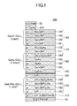
- Fig. 1 is a cross-sectional diagram illustrating a compound-semiconductor photovoltaic cell 100 according to a first embodiment.
- the compound-semiconductor photovoltaic cell 100 is a triple-junction type photovoltaic cell in which the GaInPAs cell 120 (1.0 eV), the GaAs cell 160 (1.42 eV), and the GaInP cell 180 (1.9 eV) are directly connected.
- the GaAs-based photoelectric conversion cell is a photoelectric conversion cell almost lattice matching with GaAs or Ge, a lattice constant of which is close to GaAs, and formed of a material system, a crystal of which can be grown on the GaAs substrate or a Ge substrate.
- a material which almost lattice matches with GaAs or Ge, a lattice constant of which is close to GaAs, and a crystal of which can be grown on the GaAs substrate or on the Ge substrate will be called a "GaAs lattice matching-based material”
- a cell formed of the GaAs lattice matching-based material will be called a "GaAs lattice matching-based material cell”.
- the GaInPAs cell 120 is an InP-based photoelectric conversion cell
- the GaAs cell 160 and the GaInP cell 180 are GaAs-based photoelectric conversion cells.
- the InP substrate 110 is an example of a compound-semiconductor substrate or a first compound-semiconductor substrate.
- the GaInPAs cell 120 is an example of a first photoelectric conversion cell manufactured of a first compound-semiconductor material.
- junction layer 130 is an example of a first junction layer manufactured of a second compound-semiconductor material and laminated on the GaInPAs cell 120.
- the junction layer 140 is an example of a second junction layer manufactured of a third compound-semiconductor material.
- the junction layers 130 and 140 function also as tunnel junction layers.
- the GaAs cell 160 and the GaInP cell 180 are examples of plural second photoelectric conversion cells manufactured of a fourth compound-semiconductor material.
- InP substrate 110 for example, a wafer of a single crystal of p-type indium phosphide may be used.
- impurity for example, zinc (Zn) or the like may be used.
- the GaInPAs cell 120 is configured with crystalline layers of GaInPAs which lattice match with InP.
- the InP layer 121, the Ga(x)InP(y)As layer 122, the Ga(x)InP(y)As layer 123 and the [Al(x)Ga](y)InAs layer 124 are laminated in this order.
- the InP layer 121 is a BSF (Back Surface Field) layer arranged on a deep side in the light incident direction.
- a p-n junction in the GaInPAs cell 120 is structured by the Ga(x)InP(y)As layer 122 and the Ga(x)InP(y)As layer 123.
- the [Al(x)Ga](y)InAs layer 124 is a window layer arranged on a near side in the light incident direction (light incident side).
- the GaInPAs cell 120 may be regarded as a cell, which is configured with the Ga(x)InP(y)As layer 122 and the Ga(x)InP(y)As layer 123 that structure the p-n junction, on the light incident side of the GaInPAs cell 120 the [Al(x)Ga](y)InAs layer 124 is formed, and on the deep side in the light incident direction the InP layer 121 is formed.
- the InP layer 121 has a band gap greater than a band gap (1.0 eV) of the p-type Ga(x)InP(y)As layer 122 and the n-type Ga(x)InP(y)As layer 123, since the InP layer 121 is used as the BSF layer.
- a band gap 1.0 eV
- zinc (Zn) may be used for the impurity of the InP layer 121.
- a conductivity type becomes p-type.
- Ga(x)InP(y)As layer 123 for example, by using Si for the impurity, a conductivity type becomes n-type.
- a ratio of Ga, x, and a ratio of P, y are adjusted so that the band gaps are 1.0 eV.
- the [Al(x)Ga](y)InAs layer 124 has a band gap greater than the band gaps (1.0 eV) of the Ga(x)InP(y)As layer 122 and the Ga(x)InP(y)As layer 123, since the [Al(x)Ga](y)InAs layer 124 is used as a window layer.
- the band gap of the [Al(x)Ga](y)InAs layer 124 is set to 1.5 eV, for example.
- Si may be used for the impurity of the [Al(x)Ga](y)InAs layer 124.
- AlGaInAs lattice matches with InP it is suitable for being laminated on the Ga(x)InP(y)As layer 123.
- the junction layer 130 is joined to the junction layer 140 in the process of manufacturing the compound-semiconductor photovoltaic cell 100 by a cleaning treatment and a surface activation treatment.
- the compound-semiconductor photovoltaic cell 100 is manufactured by joining the two laminated bodies.
- junction layer 130 is formed on an uppermost surface of one of the two laminated bodies, and the junction layer 140 is formed on an uppermost surface of the other laminated body.
- an n + -type InP layer is used as the junction layer 130.
- An impurity concentration of the junction layer 130 is set to be higher than an impurity concentration of the [Al(x)Ga](y)InAs layer 124. Therefore, a conductivity type of the junction layer 130 is n + -type.
- a band gap of the InP layer used as the junction layer 130 is 1.35 eV.
- the band gap of the InP layer used as the junction layer 130 is 1.35 eV.
- a Ga(x)InP layer in which Ga is added may be used as the junction layer 130, and the band gap may be made greater than 1.35 eV by increasing a composition ratio of Ga.
- a material used for the junction layer 130 preferably has a band gap which is greater than or equal to the band gap (1.42 eV) of the GaAs cell 160 which is arranged on an incident side (upstream side) of the junction layer 130 in the light incident direction.
- the junction layer 140 is joined to the junction layer 130 on the side of the InP substrate 110 in the process of manufacturing the compound-semiconductor photovoltaic cell 100 by a cleaning treatment and a surface activation treatment.
- an n + -type GaPAs layer may be used as the junction layer 140.
- a band gap of the GaPAs layer is greater than the band gap (1.42 eV) of the GaAs cell 160.
- the GaPAs layer applies a tensile strain to the GaAs substrate, but there is not a problem when it is within a range of critical film thickness, and it can be used as the junction layer 140.
- An impurity concentration of the junction layer 140 is set in the same way as the junction layer 130.
- the band gap of the GaPAs is 1.47 eV.
- junction layer 140 is laminated on the GaAs cell 160.
- the GaAs cell 160 is formed between the junction layer 140 and the tunnel junction layer 170.
- the GaAs cell 160 includes a p-type Ga(x)InP layer 161, a p-type GaAs layer 162, an n-type GaAs layer 163 and an n-type [Al(x)Ga](y)InP layer 164.
- the Ga(x)InP layer 161, the GaAs layer 162, the GaAs layer 163 and the [Al(x)Ga](y)InP layer 164 have a configuration of being laminated on a surface of the junction layer 140 in this order.
- the GaAs cell 160 is, in an actual manufacturing process, for example, laminated on the tunnel junction layer 170 in a state of being turned upside down.
- the Ga(x)InP layer 161 is a BSF (Back Surface Field) layer arranged on a deep side in the light incident direction.
- a p-n junction in the GaAs cell 160 is structured by the GaAs layer 162 and the GaAs layer 163.
- the [Al(x)Ga](y)InP layer 164 is a window layer arranged on a near side in the light incident direction (light incident side).
- the GaAs cell 160 may be regarded as a cell, which is configured with the GaAs layer 162 and the GaAs layer 163 that structure the p-n junction, on the light incident side of the GaAs cell 160 the [Al(x)Ga](y)InP layer 164 is formed, and on the deep side in the light incident direction the Ga(x)InP layer 161 is formed.
- the Ga(x)InP layer 161 has only to have a band gap greater than or equal to a band gap (1.42 eV) of the p-type GaAs layer 162 and the n-type GaAs layer 163, since the Ga(x)InP layer 161 is used as the BSF layer.
- a band gap 1.42 eV
- Zn Zn may be used for the impurity of the Ga(x)InP layer 161.
- a conductivity type becomes p-type.
- a conductivity type becomes n-type.
- the band gaps of the GaAs layer 162 and the GaAs layer 163 are 1.42 eV.
- the [Al(x)Ga](y)InP layer 164 has a band gap greater than the band gaps (1.42 eV) of the p-type GaAs layer 162 and the n-type GaAs layer 163, since the [Al(x)Ga](y)InP layer 164 is used as a window layer.
- the [Al(x)Ga](y)InP layer 164 has only to have a band gap greater than or equal to the band gap (1.42 eV) of the p-type GaAs layer 162 and the n-type GaAs layer 163.
- the impurity of the [Al(x)Ga](y)InP layer 164 for example, Si may be used.
- the tunnel junction layer 170 is arranged between the GaAs cell 160 and the GaInP cell 180.
- a part above the boundary of the junction layers 130 and 140 of the compound-semiconductor photovoltaic cell 100 shown in Fig. 1 is manufactured, for example, by serially laminating in a state of being turned upside down, the tunnel junction layer 170 is laminated on the GaInP cell 180.
- the tunnel junction layer 170 includes an n-type Ga(x)InP layer 171, and a p-type Al(x)GaAs layer 172.
- n-type Ga(x)InP layer 171 and p-type Al(x)GaAs layer 172 form a thin p-n junction which is doped at high concentration.
- Both the Ga(x)InP layer 171 and the Al(x)GaAs layer 172 are doped at higher concentration than the GaInP cell 180.
- the tunnel junction layer 170 is a junction layer arranged so that an electric current flows between the p-type Ga(x)InP layer 182 in GaInP cell 180 and the n-type GaAs layer 163 in the GaAs cell 160 by the tunnel junction.
- the GaInP cell 180 is formed between the tunnel junction layer 170 and the contact layer 40A.
- the GaInP cell 180 includes a p-type Al(x)InP layer 181, a p-type Ga(x)InP layer 182, an n-type Ga(x)InP layer 183 and an n-type Al(x)InP layer 184.
- the Al(x)InP layer 181, the Ga(x)InP layer 182, the Ga(x)InP layer 183 and the Al(x)InP layer 184 are laminated on a surface of the tunnel junction layer 170 in this order.
- the GaInP cell 180 is, in an actual manufacturing process, for example, laminated on a GaAs contact layer 40A on a GaAs substrate, which is not shown, in a state of being turned upside down.
- the GaInP cell 180 is configured with crystalline layers of GaInP which lattice matches with GaAs.
- the Al(x)InP layer 184, the Ga(x)InP layer 183, the Ga(x)InP layer 182 and the Al(x)InP layer 181 are laminated in this order.
- the GaInP cell 180 may be regarded as a cell, which is configured with the Ga(x)InP layer 182 and the Ga(x)InP layer 183 that structure the p-n junction, on the light incident side of which the Al(x)InP layer 184 is formed, and on the deep side of which in the light incident direction the Al(x)InP layer 181 is formed.
- the Al(x)InP layer 181 only has to have a band gap greater than or equal to a band gap (1.9 eV) of the p-type Ga(x)InP layer 182 and the n-type Ga(x)InP layer 183, since the Al(x)InP layer 181 is used as the BSF layer.
- a band gap 1.9 eV
- Zn may be used for the impurity of the Al(x)InP layer 181.
- a conductivity type becomes p-type.
- Ga(x)InP layer 183 for example, by using Si for the impurity, a conductivity type becomes n-type.
- the band gaps of the Ga(x)InP layer 182 and the Ga(x)InP layer 183 are 1.9 eV.
- the Al(x)InP layer 184 has a band gap greater than the band gaps (1.9 eV) of the p-type Ga(x)InP layer 182 and the n-type Ga(x)InP layer 183, since the Al(x) InP layer 184 is used as a window layer.
- the Al(x)InP layer 184 has only to have a band gap greater than or equal to the band gap (1.9 eV) of the p-type Ga(x)InP layer 182 and the n-type Ga(x)InP layer 183.
- the impurity of the Al(x)InP layer 184 for example, Si may be used.
- the contact layer 40A is a layer laminated on the GaInP cell 180 in order to perform an ohmic connection to the electrode 50.
- a gallium arsenide (GaAs) layer is used for the contact layer 40A.
- the electrode 50 is, for example, a metallic thin film, such as
- Figs. 2A to 3B are diagrams illustrating the manufacturing method of the compound-semiconductor photovoltaic cell 100 according to the first embodiment.
- a laminated body 100B is manufactured using an InP substrate 110, while manufacturing a laminated body 100A using a GaAs substrate 20.
- the GaAs substrate 20 is an example of a second compound-semiconductor substrate.
- a GaInP cell 180 included in the laminated body 100A is configured with crystalline layers of GaInP which lattice match with GaAs, and is formed on the GaAs substrate 20.
- a GaInPAs cell 120 included in the laminated body 100B is configured with crystalline layers of GaInPAs which lattice matches with InP, and is formed on the InP substrate 110.
- the compound-semiconductor photovoltaic cell 100 according to the first embodiment is manufactured by directly joining the laminated body 100A and the laminated body 100B, lattice constants of which are different from each other.
- the lattice constant of InP is about 0.587 nm or 5.87 ⁇ (angstroms)
- the lattice constant of GaAs is about 0.565 nm or 5.65 ⁇ , it is only necessary to adjust compositions so that a GaAs cell 160 and a GaInP cell 180, which are formed on the GaAs substrate 20, have lattice constants quite close to the lattice constant (about 5.65 ⁇ ) of GaAs.
- the laminated body 100A is manufactured by laminating, using MOCVD (Metal Organic Chemical Vapor Deposition) method, on the GaAs substrate 20, a Ga(x)InP etching stop layer 30, an n + -type GaAs contact layer 40, the GaInP cell 180, the tunnel junction layer 170, the GaAs cell 160 and the junction layer 140.
- MOCVD Metal Organic Chemical Vapor Deposition
- the lower side having the GaAs substrate 20 is a light incident side. Since the laminated body 100A is turned upside down upon joining to the laminated body 100B later, the laminated body 100A grows from an opposite direction with respect to the vertical relationship shown in Fig. 1 .
- the laminated bodies 100A and 100B are manufactured through epitaxial growth by MOCVD method.
- GaIn(P)As represents both a composition including P and a composition not including P. That is, GaIn(P)As is an expression including both GaInPAs and GaInAs. Therefore, a GaInAs cell may be used instead of the GaInPAs cell 120.
- the band gap of the Ga(x)InP layer used as the junction layer 230 is 1.42 eV
- the band gap of the Ga(x)InP layer used as the junction layer 230 may be made greater than 1.42 eV by increasing the composition ratio of Ga.
- the GaInP layer (junction layer 230) having a tensile strain is formed with a thickness less than the thickness in which a lattice relaxation occurs.
- conductive nanoparticles are self-arranged on a junction interface using a phase separation array of block copolymer.
- a nano-array of Pd, Au, Pt, Ag or the like is possible.
- metal ions such as Pd 2+ (palladium)
- metal ions are selectively formed on the block copolymer.
- a block copolymer template is removed and a self-arranged nanoparticle array is formed.
- Light is transmitted in a part without nano particles.
- an incident direction of light is a direction from an upper part to a lower part in the drawing (direction from the GaInP cell 180 to the GaInAs cell 410).
- a band gap between the p-type Ga(x)InAs layer 412 and n-type Ga(x)InAs layer 413 is 0.75 eV.
- the tunnel junction layer 420 is formed between the GaInPAs cell 120 and the GaInAs cell 410.
- the tunnel junction layer 420 includes an n + -type InP layer 421 and a p + -type Al(x)InAs layer 422.
- n + -type InP layer 421 and the p + -type Al(x)InAs layer 422 form a thin p-n junction which is doped at high concentration.
- Both the InP layer 421 of the tunnel junction layer 420 and the Al(x)InAs layer 422 are doped at higher concentration than the GaInPAs cell 120.
- the tunnel junction layer 420 is a junction layer arranged so that an electric current flows between the p-type Ga(x)InP(y)As layer 122 of the GaInPAs cell 120 and the n-type Ga(x)InAs layer 413 of the GaInAs cell 410 by tunnel junction.
- the compound-semiconductor photovoltaic cell 400 according to the fourth embodiment has a combination of band gaps of 1.9 eV/1.42 eV/1.0 eV/0.75 eV according to four photoelectric conversion cells of the GaInP cell 180, the GaAs cell 160, the GaInPAs cell 120 and the GaInAs cell 410.
Landscapes
- Photovoltaic Devices (AREA)
Abstract
Description
- The disclosures herein generally relate to a compound-semiconductor photovoltaic cell and a manufacturing method of the compound-semiconductor photovoltaic cell.
- Since band gap energy or a lattice constant of a compound-semiconductor varies depending on material composition, multi-junction type photovoltaic cells in which energy conversion efficiency is enhanced by sharing a wavelength range of solar light have been manufactured.
- At present, triple-junction photovoltaic cells including a Ge cell/Ga(In)As cell/GaInP cell using a lattice matching material on a Ge substrate, which has almost the same lattice constant as gallium arsenide (GaAs), having band gaps for respective cells of 1.88 eV/1.40 eV/0.67 eV, are generally used.
- A compound-semiconductor photovoltaic cell has an efficiency which is about twice an efficiency of a silicon (Si)-based photovoltaic cell. However, by reason of cost of a substrate, small size of the substrate or the like, the compound-semiconductor photovoltaic cell is several orders of magnitude more expensive than the Si-based photovoltaic cell. Therefore, the compound-semiconductor photovoltaic cells have been used for a special purpose, such as an artificial satellite in space, for example.
- Recently, a compound-semiconductor photovoltaic cell has been put to practical use for a terrestrial application (for general purpose on earth), by combining an inexpensive plastic lens and a small-sized photovoltaic cell, forming a concentration type cell, reducing an amount of compound-semiconductor which is more expensive than a normal planar cell, and realizing cost reduction.
- However, power generation costs of photovoltaic cells including Si are still high, further cost reduction is important, and enhancement of energy conversion efficiency and reduction of manufacturing post are being studied.
- As described above, a band-gap balance of the currently prevailing lattice-matching type triple-junction photovoltaic cell using a Ge substrate is not optimum from a viewpoint of an electric current band gap. A configuration, in which a band gap of a bottom cell in increased, has promise.
- Proceedings of the 29st IEEE Photovoltaic Specialists Conference (2010) pp. 412-417 discloses, as an example of high efficiency, a triple-junction photovoltaic cell in which band gaps of the respective cells are set to 1.9 eV/1.42 eV/1.0 eV, aiming at optimization of the band gap balance.
- For the cell of 1.9 eV and the cell of 1.42 eV, GaInP and GaAs which lattice match with a GaAs substrate are used, respectively. On the other hand, for the cell of 1.0 eV, a GaInAs cell, which does not lattice match with the GaAs substrate and causes lattice mismatch of about 2% to occur, is used. In order to realize the above configuration, a crystal grows in an opposite direction to those of normal photovoltaic cells.
- Specifically, on the GaAs substrate, it grows in an order of a GaInP cell and a GaAs cell. Next, it causes the GaInAs cell to grow via a lattice relaxation buffer layer for changing lattice constant difference. Then, a surface is adhered to a support substrate, and finally by removing the GaAs substrate a triple-junction photovoltaic cell is manufactured. Light incidence is on a side of the GaInP cell in which band gap is great.
- Moreover, Japanese Published Patent Application No.
2002-289884 - Moreover, Applied Physics Letters, 101, 191111 (2012) discloses a photovoltaic cell made by a series junction method using an electrically-conductive nanoparticle array. A GaAs substrate has a photovoltaic cell and an InP substrate which are connected via a Pd nanoparticle array using a VDW (Van-der-Waals) method. Electric current flows via ohmic contact of nanoparticles and semiconductor.
- Moreover, publication of
US Patent Application No. 2012/0138116 discloses a photovoltaic cell formed by directly joining a surface of a GaAs substrate on which a GaInP top cell is formed and a surface of an InP substrate on which a GaInAs bottom cell is formed. On the GaAs substrate, a cell of a short wavelength region can be formed easily using a lattice matching material, and on the InP substrate, a long wavelength region can be formed easily using a lattice matching material. - It is a general object of at least one embodiment of the present invention to provide a compound-semiconductor photovoltaic cell and a manufacturing method of the compound-semiconductor photovoltaic cell that substantially obviate one or more problems caused by the limitations and disadvantages of the related art.
- In one embodiment, a compound-semiconductor photovoltaic cell includes a compound-semiconductor substrate; one or more first photoelectric conversion cells formed of a first compound-semiconductor material and laminated on the compound-semiconductor substrate; a first junction layer formed of a second compound-semiconductor material and laminated on the one or more first photoelectric conversion cells; a second junction layer formed of a third compound-semiconductor material and joined to the first junction layer directly or indirectly; and one or more second photoelectric conversion cells formed of a fourth compound-semiconductor material, joined to the one or more first photoelectric conversion cells via the first junction layer and the second junction layer, and arranged on a light incident side of the one or more first photoelectric conversion cells in a light incident direction. Band gaps of the one or more first photoelectric conversion cells and the one or more second photoelectric conversion cells are made smaller from the incident side toward a deep side in the light incident direction in order. In a case of a single second photoelectric conversion cell, a band gap of the second junction layer is greater than or equal to a band gap of the second photoelectric conversion cell, and in a case of plural second photoelectric conversion cells, the band gap of the second junction layer is greater than or equal to a band gap of at least one second conversion cell of the plural second photoelectric conversion cells. The one or more second photoelectric conversion cells are gallium arsenide (GaAs)-based photovoltaic cells, and the second junction layer is a gallium phosphide arsenide (GaPAs) layer.
- In another embodiment, a manufacturing method of a compound-semiconductor photovoltaic cell includes forming one or more first photoelectric conversion cells of a first compound-semiconductor material on a first compound-semiconductor substrate; forming a first junction layer of a second compound-semiconductor material on the one or more first photoelectric conversion cells; forming one or more second photoelectric conversion cells of a fourth compound-semiconductor material which are arranged on a light incident side of the one or more first photoelectric conversion cells in a light incident direction on a second compound-semiconductor substrate; forming a second junction layer of a third compound-semiconductor material on the one or more second photoelectric conversion cells; joining the first junction layer to the second junction layer directly or indirectly; and removing the second compound-semiconductor substrate. Band gaps of the one or more first photoelectric conversion cells and the one or more second photoelectric conversion cells are made smaller from the incident side toward a deep side in the light incident direction in order. In a case of a single second photoelectric conversion cell, a band gap of the second junction layer is greater than or equal to a band gap of the second photoelectric conversion cell, and in a case of plural second photoelectric conversion cells, the band gap of the second junction layer is greater than or equal to a band gap of at least one second conversion cell of the plural second photoelectric conversion cells. The one or more second photoelectric conversion cells are GaAs-based photovoltaic cells, and the second junction layer is a GaPAs layer.
- According to the embodiment of the present application, a compound-semiconductor photovoltaic cell achieving high efficiency, and a manufacturing method of the compound-semiconductor photovoltaic cell can be provided.
- Other objects and further features of embodiments will become apparent from the following detailed description when read in conjunction with the accompanying drawings, in which:
-
Fig. 1 is a cross-sectional diagram illustrating an example of a compound-semiconductorphotovoltaic cell 100 according to a first embodiment; -
Figs. 2A and 2B are diagrams illustrating an example of a manufacturing method of the compound-semiconductorphotovoltaic cell 100 according to the first embodiment; -
Figs. 3A and 3B are diagrams illustrating another example of the manufacturing method of the compound semiconductorphotovoltaic cell 100 according to the first embodiment; -
Fig. 4 is a cross-sectional diagram illustrating an example of a compound-semiconductorphotovoltaic cell 200 according to a second embodiment; -
Fig. 5 is a cross-sectional diagram illustrating an example of a compound-semiconductorphotovoltaic cell 201 according to a variation of the second embodiment; -
Fig. 6 is a cross-sectional diagram illustrating an example of a compound-semiconductorphotovoltaic cell 300 according to a third embodiment; and -
Fig. 7 is a cross-sectional diagram illustrating an example of a compound-semiconductorphotovoltaic cell 400 according to a fourth embodiment. - In the following, embodiments to which an compound-semiconductor photovoltaic cell and a manufacturing method of the compound-semiconductor photovoltaic cell according to the present invention are applied will be described with reference to the accompanying drawings.
-
Fig. 1 is a cross-sectional diagram illustrating a compound-semiconductorphotovoltaic cell 100 according to a first embodiment. - The compound-semiconductor
photovoltaic cell 100 includes anelectrode 10, anInP substrate 110, a GaInPAscell 120, ajunction layer 130, ajunction layer 140, aGaAs cell 160, atunnel junction layer 170, aGaInP cell 180, acontact layer 40A and anelectrode 50. - The compound-semiconductor
photovoltaic cell 100 according to the first embodiment is a triple-junction type photovoltaic cell in which the GaInPAs cell 120 (1.0 eV), the GaAs cell 160 (1.42 eV), and the GaInP cell 180 (1.9 eV) are directly connected. - Here, a cell included in the compound-semiconductor
photovoltaic cell 100 includes an InP (indium phosphide)-based photoelectric conversion cell and a GaAs (gallium arsenide)-based photoelectric conversion cell. The InP-based photoelectric conversion cell is a photoelectric conversion cell almost lattice matching with InP and formed of a material system, a crystal of which can be grown on theInP substrate 110. Here, a material which almost lattice matches with InP, and a crystal of which can be grown on theInP substrate 110 will be called an "InP lattice matching-based material", and a cell formed of the InP lattice matching-based material will be called an "InP lattice matching-based material cell". - Moreover, the GaAs-based photoelectric conversion cell is a photoelectric conversion cell almost lattice matching with GaAs or Ge, a lattice constant of which is close to GaAs, and formed of a material system, a crystal of which can be grown on the GaAs substrate or a Ge substrate. Here, a material which almost lattice matches with GaAs or Ge, a lattice constant of which is close to GaAs, and a crystal of which can be grown on the GaAs substrate or on the Ge substrate will be called a "GaAs lattice matching-based material", and a cell formed of the GaAs lattice matching-based material will be called a "GaAs lattice matching-based material cell".
- Meanwhile, the above-described configurations are the same also in second to fourth embodiments.
- In the compound-semiconductor
photovoltaic cell 100, the GaInPAscell 120 is an InP-based photoelectric conversion cell, and theGaAs cell 160 and theGaInP cell 180 are GaAs-based photoelectric conversion cells. - Here, the
InP substrate 110 is an example of a compound-semiconductor substrate or a first compound-semiconductor substrate. TheGaInPAs cell 120 is an example of a first photoelectric conversion cell manufactured of a first compound-semiconductor material. - Moreover, the
junction layer 130 is an example of a first junction layer manufactured of a second compound-semiconductor material and laminated on theGaInPAs cell 120. Thejunction layer 140 is an example of a second junction layer manufactured of a third compound-semiconductor material. The junction layers 130 and 140 function also as tunnel junction layers. TheGaAs cell 160 and theGaInP cell 180 are examples of plural second photoelectric conversion cells manufactured of a fourth compound-semiconductor material. - In
Fig. 1 , an incident direction of light is a direction from an upper part to a lower part in the drawing (direction from theGaInP cell 180 to the GaInPAs cell 120). - The
electrode 10 is a lower electrode positioned on a deep side in the light incident direction. For theelectrode 10, for example, an electrode in which metal layers of Ti/Pt/Au or the like may be used. - For the
InP substrate 110, for example, a wafer of a single crystal of p-type indium phosphide may be used. For impurity, for example, zinc (Zn) or the like may be used. - The
GaInPAs cell 120 is formed on a surface of theInP substrate 110. TheGaInPAs cell 120 includes a p-type InP layer 121, a p-type Ga(x)InP(y)Aslayer 122, an n-type Ga(x)InP(y)Aslayer 123, and an n-type [Al(x)Ga](y)InAs layer 124. - The
GaInPAs cell 120 is configured with crystalline layers of GaInPAs which lattice match with InP. TheInP layer 121, the Ga(x)InP(y)Aslayer 122, the Ga(x)InP(y)Aslayer 123 and the [Al(x)Ga](y)InAs layer 124 are laminated in this order. - The
InP layer 121 is a BSF (Back Surface Field) layer arranged on a deep side in the light incident direction. A p-n junction in theGaInPAs cell 120 is structured by the Ga(x)InP(y)Aslayer 122 and the Ga(x)InP(y)Aslayer 123. The [Al(x)Ga](y)InAs layer 124 is a window layer arranged on a near side in the light incident direction (light incident side). - Here, the
GaInPAs cell 120 may be regarded as a cell, which is configured with the Ga(x)InP(y)Aslayer 122 and the Ga(x)InP(y)Aslayer 123 that structure the p-n junction, on the light incident side of theGaInPAs cell 120 the [Al(x)Ga](y)InAs layer 124 is formed, and on the deep side in the light incident direction theInP layer 121 is formed. - The
InP layer 121 has a band gap greater than a band gap (1.0 eV) of the p-type Ga(x)InP(y)Aslayer 122 and the n-type Ga(x)InP(y)Aslayer 123, since theInP layer 121 is used as the BSF layer. For the impurity of theInP layer 121, for example, zinc (Zn) may be used. - In the Ga(x)InP(y)As
layer 122, for example, by using Zn for the impurity, a conductivity type becomes p-type. - In the Ga(x)InP(y)As
layer 123, for example, by using Si for the impurity, a conductivity type becomes n-type. - In the Ga(x)InP(y)As
layer 122 and the Ga(x)InP(y)Aslayer 123, a ratio of Ga, x, and a ratio of P, y, are adjusted so that the band gaps are 1.0 eV. - The [Al(x)Ga](y)
InAs layer 124 has a band gap greater than the band gaps (1.0 eV) of the Ga(x)InP(y)Aslayer 122 and the Ga(x)InP(y)Aslayer 123, since the [Al(x)Ga](y)InAs layer 124 is used as a window layer. - In the first embodiment, the band gap of the [Al(x)Ga](y)
InAs layer 124 is set to 1.5 eV, for example. For the impurity of the [Al(x)Ga](y)InAs layer 124, for example, Si may be used. - Since AlGaInAs lattice matches with InP, it is suitable for being laminated on the Ga(x)InP(y)As
layer 123. - The
junction layer 130 is joined to thejunction layer 140 in the process of manufacturing the compound-semiconductorphotovoltaic cell 100 by a cleaning treatment and a surface activation treatment. The compound-semiconductorphotovoltaic cell 100 is manufactured by joining the two laminated bodies. - The
junction layer 130 is formed on an uppermost surface of one of the two laminated bodies, and thejunction layer 140 is formed on an uppermost surface of the other laminated body. By joining thejunction layer 130 and thejunction layer 140, the compound-semiconductorphotovoltaic cell 100, as shown inFig. 1 , is manufactured. - As the
junction layer 130, an n+-type InP layer is used. An impurity concentration of thejunction layer 130 is set to be higher than an impurity concentration of the [Al(x)Ga](y)InAs layer 124. Therefore, a conductivity type of thejunction layer 130 is n+-type. - A band gap of the InP layer used as the
junction layer 130 is 1.35 eV. Here, an embodiment in which the band gap of the InP layer used as thejunction layer 130 is 1.35 eV will be explained. However, a Ga(x)InP layer in which Ga is added may be used as thejunction layer 130, and the band gap may be made greater than 1.35 eV by increasing a composition ratio of Ga. - A material used for the
junction layer 130 preferably has a band gap which is greater than or equal to the band gap (1.42 eV) of theGaAs cell 160 which is arranged on an incident side (upstream side) of thejunction layer 130 in the light incident direction. - Moreover, a band gap of the [Al(x)Ga](y)
InAs layer 124 which is a window layer of theGaInPAs cell 120 is set to 1.5 eV, for example, so that light transmitted through thejunction layer 130 surely reaches the Ga(x)InP(y)Aslayer 122 and the Ga(x)InP(y)Aslayer 123 of theGaInPAs cell 120. - The
junction layer 140 is joined to thejunction layer 130 on the side of theInP substrate 110 in the process of manufacturing the compound-semiconductorphotovoltaic cell 100 by a cleaning treatment and a surface activation treatment. As thejunction layer 140, an n+-type GaPAs layer may be used. A band gap of the GaPAs layer is greater than the band gap (1.42 eV) of theGaAs cell 160. - The GaPAs layer applies a tensile strain to the GaAs substrate, but there is not a problem when it is within a range of critical film thickness, and it can be used as the
junction layer 140. An impurity concentration of thejunction layer 140 is set in the same way as thejunction layer 130. The band gap of the GaPAs is 1.47 eV. - Since a part above the boundary of the junction layers 130 and 140 of the compound-semiconductor
photovoltaic cell 100 shown inFig. 1 is manufactured, for example, by serially laminating in a state of being turned upside down, thejunction layer 140 is laminated on theGaAs cell 160. - The
GaAs cell 160 is formed between thejunction layer 140 and thetunnel junction layer 170. - The
GaAs cell 160 includes a p-type Ga(x)InP layer 161, a p-type GaAs layer 162, an n-type GaAs layer 163 and an n-type [Al(x)Ga](y)InP layer 164. - The Ga(x)
InP layer 161, theGaAs layer 162, theGaAs layer 163 and the [Al(x)Ga](y)InP layer 164 have a configuration of being laminated on a surface of thejunction layer 140 in this order. TheGaAs cell 160 is, in an actual manufacturing process, for example, laminated on thetunnel junction layer 170 in a state of being turned upside down. - For this reason, in the actual manufacturing process, they are laminated on the
tunnel junction layer 170 in the order of, for example, the [Al(x)Ga](y)InP layer 164, theGaAs layer 163, theGaAs layer 162 and the Ga(x)InP layer 161. - The Ga(x)
InP layer 161 is a BSF (Back Surface Field) layer arranged on a deep side in the light incident direction. A p-n junction in theGaAs cell 160 is structured by theGaAs layer 162 and theGaAs layer 163. The [Al(x)Ga](y)InP layer 164 is a window layer arranged on a near side in the light incident direction (light incident side). - Here, the
GaAs cell 160 may be regarded as a cell, which is configured with theGaAs layer 162 and theGaAs layer 163 that structure the p-n junction, on the light incident side of theGaAs cell 160 the [Al(x)Ga](y)InP layer 164 is formed, and on the deep side in the light incident direction the Ga(x)InP layer 161 is formed. - The Ga(x)
InP layer 161 has only to have a band gap greater than or equal to a band gap (1.42 eV) of the p-type GaAs layer 162 and the n-type GaAs layer 163, since the Ga(x)InP layer 161 is used as the BSF layer. For the impurity of the Ga(x)InP layer 161, for example, Zn may be used. - In the
GaAs layer 162, for example, by using Zn for the impurity, a conductivity type becomes p-type. - In the
GaAs layer 163, for example, by using Si for the impurity, a conductivity type becomes n-type. - The band gaps of the
GaAs layer 162 and theGaAs layer 163 are 1.42 eV. - The [Al(x)Ga](y)
InP layer 164 has a band gap greater than the band gaps (1.42 eV) of the p-type GaAs layer 162 and the n-type GaAs layer 163, since the [Al(x)Ga](y)InP layer 164 is used as a window layer. - In the first embodiment, the [Al(x)Ga](y)
InP layer 164 has only to have a band gap greater than or equal to the band gap (1.42 eV) of the p-type GaAs layer 162 and the n-type GaAs layer 163. For the impurity of the [Al(x)Ga](y)InP layer 164, for example, Si may be used. - The
tunnel junction layer 170 is arranged between theGaAs cell 160 and theGaInP cell 180. A part above the boundary of the junction layers 130 and 140 of the compound-semiconductorphotovoltaic cell 100 shown inFig. 1 is manufactured, for example, by serially laminating in a state of being turned upside down, thetunnel junction layer 170 is laminated on theGaInP cell 180. - The
tunnel junction layer 170 includes an n-type Ga(x)InP layer 171, and a p-type Al(x)GaAs layer 172. For an impurity for causing a conductivity type to become n-type, for example, tellurium (Te) may be used. For an impurity for causing a conductivity type to become p-type, for example, carbon (C) may be used. The n-type Ga(x)InP layer 171 and the p-type Al(x)GaAs layer 172 form a thin p-n junction which is doped at high concentration. - Both the Ga(x)
InP layer 171 and the Al(x)GaAs layer 172 are doped at higher concentration than theGaInP cell 180. Thetunnel junction layer 170 is a junction layer arranged so that an electric current flows between the p-type Ga(x)InP layer 182 inGaInP cell 180 and the n-type GaAs layer 163 in theGaAs cell 160 by the tunnel junction. - The
GaInP cell 180 is formed between thetunnel junction layer 170 and thecontact layer 40A. - The
GaInP cell 180 includes a p-type Al(x)InP layer 181, a p-type Ga(x)InP layer 182, an n-type Ga(x)InP layer 183 and an n-type Al(x)InP layer 184. - The Al(x)
InP layer 181, the Ga(x)InP layer 182, the Ga(x)InP layer 183 and the Al(x)InP layer 184 are laminated on a surface of thetunnel junction layer 170 in this order. TheGaInP cell 180 is, in an actual manufacturing process, for example, laminated on aGaAs contact layer 40A on a GaAs substrate, which is not shown, in a state of being turned upside down. - The
GaInP cell 180 is configured with crystalline layers of GaInP which lattice matches with GaAs. In an actual manufacturing process, for example, the Al(x)InP layer 184, the Ga(x)InP layer 183, the Ga(x)InP layer 182 and the Al(x)InP layer 181 are laminated in this order. - The Al(x)
InP layer 181 is a BSF (Back Surface Field) layer arranged on a deep side in the light incident direction. A p-n junction in theGaInP cell 180 is structured by the Ga(x)InP layer 182 and the Ga(x)InP layer 183. The Al(x)InP layer 184 is a window layer arranged on a near side in the light incident direction (light incident side). - Here, the
GaInP cell 180 may be regarded as a cell, which is configured with the Ga(x)InP layer 182 and the Ga(x)InP layer 183 that structure the p-n junction, on the light incident side of which the Al(x)InP layer 184 is formed, and on the deep side of which in the light incident direction the Al(x)InP layer 181 is formed. - The Al(x)
InP layer 181 only has to have a band gap greater than or equal to a band gap (1.9 eV) of the p-type Ga(x)InP layer 182 and the n-type Ga(x)InP layer 183, since the Al(x)InP layer 181 is used as the BSF layer. For the impurity of the Al(x)InP layer 181, for example, Zn may be used. - In the Ga(x)
InP layer 182, for example, by using Zn for the impurity, a conductivity type becomes p-type. - In the Ga(x)
InP layer 183, for example, by using Si for the impurity, a conductivity type becomes n-type. - The band gaps of the Ga(x)
InP layer 182 and the Ga(x)InP layer 183 are 1.9 eV. - The Al(x)
InP layer 184 has a band gap greater than the band gaps (1.9 eV) of the p-type Ga(x)InP layer 182 and the n-type Ga(x)InP layer 183, since the Al(x)InP layer 184 is used as a window layer. - In the first embodiment, the Al(x)
InP layer 184 has only to have a band gap greater than or equal to the band gap (1.9 eV) of the p-type Ga(x)InP layer 182 and the n-type Ga(x)InP layer 183. For the impurity of the Al(x)InP layer 184, for example, Si may be used. - The
contact layer 40A is a layer laminated on theGaInP cell 180 in order to perform an ohmic connection to theelectrode 50. For example, a gallium arsenide (GaAs) layer is used for thecontact layer 40A. - The
electrode 50 is, for example, a metallic thin film, such as - Ti/Pb/Au, and formed on the
contact layer 40A. - Next, a manufacturing method of the compound-semiconductor
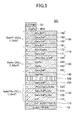
photovoltaic cell 100 according to the first embodiment will be explained with reference toFigs. 2A to 3B . -
Figs. 2A to 3B are diagrams illustrating the manufacturing method of the compound-semiconductorphotovoltaic cell 100 according to the first embodiment. - At first, as shown in
Fig. 2A , alaminated body 100B is manufactured using anInP substrate 110, while manufacturing alaminated body 100A using aGaAs substrate 20. TheGaAs substrate 20 is an example of a second compound-semiconductor substrate. - Here, a
GaInP cell 180 included in thelaminated body 100A is configured with crystalline layers of GaInP which lattice match with GaAs, and is formed on theGaAs substrate 20. Moreover, aGaInPAs cell 120 included in thelaminated body 100B is configured with crystalline layers of GaInPAs which lattice matches with InP, and is formed on theInP substrate 110. - In this way, lattice constants of the
laminated body 100A and thelaminated body 100B are different from each other. The compound-semiconductorphotovoltaic cell 100 according to the first embodiment is manufactured by directly joining thelaminated body 100A and thelaminated body 100B, lattice constants of which are different from each other. - Since the lattice constant of InP is about 0.587 nm or 5.87 Å (angstroms), it is only necessary to adjust a composition so that the
GaInPAs cell 120 formed on theInP substrate 110 has a lattice constant quite close to the lattice constant (about 5.87 Å) of InP. - Moreover, since the lattice constant of GaAs is about 0.565 nm or 5.65 Å, it is only necessary to adjust compositions so that a
GaAs cell 160 and aGaInP cell 180, which are formed on theGaAs substrate 20, have lattice constants quite close to the lattice constant (about 5.65 Å) of GaAs. - The
laminated body 100A is manufactured by laminating, using MOCVD (Metal Organic Chemical Vapor Deposition) method, on theGaAs substrate 20, a Ga(x)InPetching stop layer 30, an n+-typeGaAs contact layer 40, theGaInP cell 180, thetunnel junction layer 170, theGaAs cell 160 and thejunction layer 140. - Here, the
GaInP cell 180 includes an Al(x)InP layer 184 which lattice matches with GaAs, a Ga(x)InP layer 183, a Ga(x)InP layer 182 and an Al(x)InP layer 181. The Al(x)InP layer 181 is a BSF layer, and the Al(x)InP layer 184 is a window layer. - Moreover, the
tunnel junction layer 170 includes an Al(x)GaAs layer 172 and an Ga(x)InP layer 171. - The
GaAs cell 160 includes an [Al(x)Ga](y)InP layer 164, aGaAs layer 163, aGaAs layer 162 and a Ga(x)InP layer 161. The Ga(x)InP layer 161 is a BSF layer, and the [Al(x)Ga](y)InP layer 164 is a window layer. - Upon the lamination (growth) of the
laminated body 100A, the lower side having theGaAs substrate 20 is a light incident side. Since thelaminated body 100A is turned upside down upon joining to thelaminated body 100B later, thelaminated body 100A grows from an opposite direction with respect to the vertical relationship shown inFig. 1 . - Specifically, it serially grows from a cell of a wide band gap (GaInP cell 180) to a narrow gap cell (GaAs cell 160). Moreover, finally a p-side becomes the lower side (deep side in the light incident direction).
- Moreover, for the
laminated body 100B, theGaInPAs cell 120 and thejunction layer 130 are laminated (grown) on theInP substrate 110 by MOCVD method. In thelaminated body 100B shown inFig. 2A , a side of thejunction layer 130, which is opposite to theInP substrate 110, is a light incident side. - The
GaInPAs cell 120 includes, from a side of theInP substrate 110, anInP layer 121, a Ga(x)InP(y)Aslayer 122, a Ga(x)InP(y)Aslayer 123 and an [Al(x)Ga](y)InAs layer 124. TheInP layer 121 is a BSF layer, and the [Al(x)Ga](y)InAs layer 124 is a window layer. - As described above, the
laminated bodies - Next, as shown in
Fig. 2B , thelaminated bodies - Surfaces of the
junction layer 140 of thelaminated body 100A and thejunction layer 130 of thelaminated body 100B are subjected to a cleaning treatment and a surface activation treatment, and thejunction layer 130 and thejunction layer 140 are joined directly. The surface activation treatment is performed by a nitrogen (N2) plasma treatment, and the junction is performed in a vacuum at temperature of 150 °C. - According to the above-described processes, a
laminated body 100C, as shown inFig. 2B , is prepared. Thelaminated body 100C is manufactured by placing thelaminated body 100A, which is turned upside down, i.e. in a state where thejunction layer 140 is on the bottom side, on thejunction layer 130 of thelaminated body 100B, shown inFig. 2A , and joining thejunction layer 130 and thejunction layer 140. - The
laminated body 100C has a configuration in which on theInP substrate 110, theGaInPAs cell 120, thejunction layer 130, thejunction layer 140, theGaAs cell 160, thetunnel junction layer 170, theGaInP cell 180, theGaAs contact layer 40, an InPetching stop layer 30 and theGaAs substrate 20 are laminated in this order. - Next, the
GaAs substrate 20 and the GaInPetching stop layer 30 are removed from thelaminated body 100C, shown inFig. 2B by selective etching, respectively, and thereby a laminated body 100D, shown inFig. 3A , is obtained. - The
GaAs substrate 20 and the GaInPetching stop layer 30 may be etched as follows: - The
GaAs substrate 20 can be etched, for example, with a mixture of sulfuric acid (H2SO4), hydrogen peroxide (N2O2) and water (H2O) as wet etching solution. Since GaInP in the GaInPetching stop layer 30 does not dissolve in the mixture of sulfuric acid (H2SO4), hydrogen peroxide (N2O2) and water (H2O), the wet etching process can be stopped at the GaInPetching stop layer 30. - Moreover, the GaInP
etching stop layer 30 can be etched, for example, with a mixture of hydrochloric acid (HCl) and water (H2O). - As described above, the laminated body 100D, shown in
Fig. 3A , is obtained by removing theGaAs substrate 20 and the GaInPetching stop layer 30 from thelaminated body 100C (SeeFig. 2B ) by selective etching, respectively. - Next, while forming an upper electrode 50 (see
Fig. 1 ) on theGaAs contact layer 40, alower electrode 10 is formed on theInP substrate 110. - Then, the contact layer 40 (See
Fig. 3A ) other than a part located immediately below the upper electrode 50 (SeeFig. 1 ) is removed by using theupper electrode 50 as a mask, and thereby acontact layer 40A, as shown inFig. 3B , is formed. - The
contact layer 40A can be formed, for example, by etching with a mixture of sulfuric acid (H2SO4), hydrogen peroxide (H2O2) and water (H2O) as wet etching solution. Since AlInP in the Al(x)InP layer 184 does not dissolve in the mixture of sulfuric acid (H2SO4), hydrogen peroxide (H2O2) and water (H2O), the wet etching process can be stopped at the Al(x)InP layer 184 in theGaInP cell 180. - As described above, the compound-semiconductor
photovoltaic cell 100 according to the first embodiment is completed. The compound-semiconductorphotovoltaic cell 100 shown inFig. 3B is identical with the compound-semiconductorphotovoltaic cell 100 shown inFig. 1 . - The compound-semiconductor
photovoltaic cell 100 has a configuration such that solar light enters the compound-semiconductorphotovoltaic cell 100 from a side of a cell of a wide band gap (side of the GaInP cell 180). Meanwhile, an antireflection film is preferably provided on a surface of the Al(x)InP layer 184, which solar light enters. The antireflection film is omitted inFig. 3B . - As described above, the compound-semiconductor
photovoltaic cell 100 according to the first embodiment uses the GaPAs layer which is greater than the band gap (1.42 eV) of theGaAs cell 160 as ajunction layer 140. - Conventionally, GaAs (1.42 eV) or GaInP (1.9 eV) is used as a wafer junction layer such as the
junction layer 140. In a case of a GaAs wafer junction layer, a part of light transmitted through the GaAs cell (1.42 eV) is absorbed here, and efficiency decreases. - On the other hand, in the first embodiment, for a material of the junction layers 130 and 140 which serve both as wafer junction layers and as tunnel junctions, p+GaPAs/n+InP is used. Since GaPAs as the
junction layer 140 has a band gap greater than the GaAs cell 160 (1.42 eV), it is possible to cause most of light of long wavelength transmitted through theGaAs cell 160 to enter theGaInPAs cell 120. - Moreover, impurity concentrations of the tunnel junction layers and the wafer junction layers are required to be high. In the first embodiment, since the
junction layer GaAs cell 160 and theGaInPAs cell 120, a thickness of high concentration layers can be decreased and light absorption in the junction layers 130 and 140 is reduced. Therefore, a highly-efficient compound-semiconductorphotovoltaic cell 100 can be manufactured. - Moreover, the GaInP cell 180 (1.9 eV) lattice matching with GaAs has a great junctional resistance in joining to InP, and is a factor degrading efficiency. In the first embodiment of the present invention, since difference between valence band energy of p+GaPAs of the
junction layer 140 and conduction band energy of n+InP of thejunction layer 130 is less than the difference between valence band energy of p+GaInP and the conduction band energy of n+InP, the junctional resistance is low. According to the above-described property, it is possible to further enhance the efficiency. - Moreover, in the compound-semiconductor
photovoltaic cell 100 according to the first embodiment, as a window layer of theGaInPAs cell 120 formed on theInP substrate 110, the [Al(x)Ga](y)InAs layer 124 with a band gap of 1.5 eV is formed, and as thejunction layer 130 above it, the InP junction layer is formed. - Moreover, a band gap of the [Al(x)Ga](y)
InAs layer 124 which is a window layer of theGaInPAs cell 120 is set to 1.5 eV, which is greater than theGaAs cell 160, so that light transmitted through thejunction layer 130 surely reaches the Ga(x)InP(y)Aslayer 122 and the Ga(x)InP(y)Aslayer 123 of theGaInPAs cell 120. - For this reason, according to the first embodiment, a compound-semiconductor
photovoltaic cell 100 for which efficiency is enhanced and a manufacturing method of the compound-semiconductorphotovoltaic cell 100 can be provided. - Moreover, in the compound-semiconductor
photovoltaic cell 100 according to the first embodiment, in addition to setting the band gap of thejunction layer 130 as described above, a band gap of the [Al(x)Ga](y)InAs layer 124, which is a window layer of theGaInPAs cell 120, is set to 1.5 eV which is greater than that of theGaAs cell 160. - Also according to the above setting, efficiency is enhanced for the compound-semiconductor
photovoltaic cell 100. - Moreover, instead of the [Al(x)Ga](y)
InAs layer 124, which is a window layer of theGaInPAs cell 120, a thin film layer formed of Al(Ga)InAs, Al(Ga)AsSb, Al(Ga)PSb, Al(In)PSb or the like may be used. - In this case, instead of the [Al(x)Ga](y)
InAs layer 124, it is only necessary to adjust a composition so that the thin film layer of Al(Ga)InAs, Al(Ga)AsSb, Al(Ga)PSb, Al(In)PSb or the like has a band gap the same as or greater than the GaAs cell 160 (1.42 eV). - Meanwhile, in the expressions "Al(Ga)InAs", "Al(Ga)AsSb" and "Al(Ga)PSb", the notation "(Ga)" represents both a composition including Ga and a composition not including Ga. That is, "Al(Ga)InAs" is an expression including "AlGaInAs" and "AlInAs". Moreover, "Al(Ga)AsSb" is an expression including "AlGaAsSb" and "AIAsSb". Furthermore, "Al(Ga)PSb" is an expression including "AlGaPSb" and "AlPSb".
- Moreover, in the expression "Al(In)PSb", the notation "(In)" represents both a composition including In and a position not including In. That is, "Al(In)PSb" is an expression including "AlInPSb" and "AlPSb".
- Regarding a triple-junction
photovoltaic cell 100, such as the compound-semiconductorphotovoltaic cell 100 according to the first embodiment, for example, Oyo Butsuri Vol. 79, No. 5, 2010, P. 436 describes, as band gaps of three cells, a combination of 1.9 eV/1.42 eV/1.0 eV and a combination of 1.7 eV/1.2 eV/0.67 eV, which are more preferable than the triple-junction cell of (1.88 eV/1.4 eV/0.67 eV) according to the related art. - However, it is quite difficult to realize the above-described combinations of band gaps by using a lattice constant.
- In this respect, according to the first embodiment, since a compound-semiconductor
photovoltaic cell 100 is manufactured by joining two cells of lattice constants (laminated body 100A andlaminated body 100B (SeeFig. 2A )) using a direct junction method, the compound-semiconductorphotovoltaic cell 100 including cells having lattice constants which are different from each other can be easily realized. - Meanwhile, in the above description, the embodiment, in which respective cells or the like are formed on an
InP substrate 10 and aGaAs substrate 20 by MOCVD method, is explained. However, the respective cells or the like may be formed by MBE (Molecular Beam Epitaxy) method. - Moreover, in the above description, the embodiment, in which the compound-semiconductor
photovoltaic cell 100 is manufactured by usinglaminated bodies InP substrate 10 and theGaAs substrate 20, respectively, is explained. However, a combination other than theInP substrate 10 and theGaAs substrate 20 may be used. - For example, the
laminated bodies - Moreover, in the above description, the embodiment, in which as an InP lattice matching system material cell a
GaInPAs cell 120 is used, is explained. However, the InP lattice matching system material cell is not limited to theGaInPAs cell 120, but a cell expressed by "GaIn(P)As" may be used. - The notation (P) in the expression GaIn(P)As represents both a composition including P and a composition not including P. That is, GaIn(P)As is an expression including both GaInPAs and GaInAs. Therefore, a GaInAs cell may be used instead of the
GaInPAs cell 120. - Moreover, in the above description, the embodiment, in which as a GaAs lattice matching system material cell a
GaInP cell 180 is used, is explained. However, the GaAs lattice matching system material cell is not limited to theGaInP cell 180, but a cell expressed by "(Al)GaInP(As)" may be used. - The expression "(Al)GaInP(As)" includes both a composition including Al and a composition not including Al. Moreover, the expression "(Al)GaInP(As)" includes both a composition including As and a composition not including As. For this reason, it is expressed by "(Al)" and "(As)". That is, "(Al)GaInP(As)" is an expression including AlGaInP, GaInPAs and GaInP. Therefore, an AlGaInP cell or a GaInPAs cell may be used instead of the
GaInP cell 180. - In a photovoltaic cell shown in Applied Physics Letters, 101, 191111 (2012), light of long wavelength transmitted through the GaInPAs cell (1.8 eV) enters a GaInPAs cell (1.15 eV). However, on the light incident side of the GaInPAs cell (1.15 eV), an InP junction layer whose band gap is less than an absorption layer (1.8 eV) of the GaInPAs cell is formed via a Pd layer below the GaInPAs cell (1.8 eV).
- Therefore, before entering the GaInPAs cell (1.15 eV) a part of light is absorbed in the InP junction layer. This InP junction layer serves both a function as a junction layer and a function as a window layer. However, since such an InP window layer has a band gap less than the absorption layer (1.8 eV) of the GaInPAs cell, it contributes to degradation of efficiency of the photovoltaic cell.
- Moreover, in the related art described in publication of
US Patent Application No. 2012/0138116 , light of long wavelength transmitted through the GaInP cell enters the GaInAs cell. However, on the light incident side of the GaInAs cell, an InP junction layer whose band gap is less than the GaInP is formed as a junction layer which is directly connected to a GaAs epi-substrate. Therefore, before entering the GaInAs cell a part of light is absorbed in the InP junction layer. Such an InP window layer contributes to degradation of efficiency of the photovoltaic cell. - In the second embodiment, a compound-semiconductor photovoltaic cell that also solves the above-described problem is provided.
-
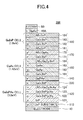
Fig. 4 is a cross-sectional diagram illustrating a compound-semiconductorphotovoltaic cell 200 according to the second embodiment. The compound-semiconductorphotovoltaic cell 200 is obtained by replacing the junction layer 130 (InP layer) in the compound-semiconductorphotovoltaic cell 100 according to the first embodiment by a junction layer 230 (Ga(x)InP layer). Since other configurations are the same as the compound-semiconductorphotovoltaic cell 100 according to the first embodiment, a difference will be explained in the following. - As the
junction layer 230, an n+-type Ga(x)InP layer is used. An impurity concentration of thejunction layer 230 is set to be higher than an impurity concentration of the [Al(x)Ga](y)InAs layer 124. Therefore, a conductivity type of thejunction layer 230 is n+-type. - The Ga(x)InP layer used as the
junction layer 230 is, for example, a GaInP layer with a Ga composition of 10% (i.e. x=0.1), a tensile strain of 0.7% and a band gap of 1.42 eV. - Here, an embodiment in which the band gap of the Ga(x)InP layer used as the
junction layer 230 is 1.42 eV will be explained. However, the band gap of the Ga(x)InP layer used as thejunction layer 230 may be made greater than 1.42 eV by increasing the composition ratio of Ga. - The Ga(x)InP layer used as the
junction layer 230 only has to have a band gap which is greater than or equal to the band gap (1.42 eV) of theGaAs cell 160 which is arranged on an incident side (upstream side) of thejunction layer 230 in the light incident direction. - That is, the band gap of the
junction layer 230 only has to be greater than or equal to the band gap of theGaAs cell 160 which is arranged on the incident side (upstream side) of thejunction layer 230 in the light incident direction. - In the compound-semiconductor
photovoltaic cell 200 according to the second embodiment, the band gap of thejunction layer 230 is set as above in order to prevent light transmitted through theGaAs cell 160 and thejunction layer 140 without absorption from being absorbed in thejunction layer 230. - That is, the above-described setting is to effectively guide solar light to the
GaInPAs cell 120 on a deep side (downstream side) of thejunction layer 230 in the light incident direction without being absorbed in thejunction layer 230. - In the compound-semiconductor
photovoltaic cell 200 according to the second embodiment, as a window layer of theGaInPAs cell 120 formed on theInP substrate 110, an [Al(x)Ga](y)InAs layer 124 with a band gap of 1.5 eV is formed, and as thejunction layer 230 further on it a GaInP junction layer is formed. - The GaInP junction layer used as the
junction layer 230 is a GaInP junction layer which has a Ga composition of 10%, a tensile strain of 0.7% and a band gap of 1.42 eV. The band gap of the junction layer 230 (1.42 eV) is set so as to be greater than or equal to a band gap (1.42 eV) of the GaAs call 160 which is a photoelectric conversion cell adjacent to thejunction layer 230 on the light incident side. - That is, the Ga(x)InP layer used as the
junction layer 230 has the above-described band gap in order to guide light transmitted through theGaAs cell 160, which is a photoelectric conversion cell adjacent on the light incident side (upstream side) of thejunction layer 230 in the light incident direction, without being absorbed, to theGaInPAs cell 120 on the deep side of thejunction layer 230 in the light incident direction. - Moreover, a band gap of the [Al(x)Ga](y)
InAs layer 124 which is a window layer of theGaInPAs cell 120 is set to 1.5 eV, which is greater than theGaAs cell 160, so that light transmitted through thejunction layer 230 surely reaches the Ga(x)InP(y)Aslayer 122 and the Ga(x)InP(y)Aslayer 123 of theGaInPAs cell 120. - In the compound-semiconductor
photovoltaic cell 200 according to the second embodiment, a Ga(x)InP layer having a band gap greater than or equal to the band gaps of theGaAs cell 160 and thejunction layer 140 is used as thejunction layer 230 in order to suppress an occurrence of energy loss. - For this reason, according to the second embodiment, a compound-semiconductor
photovoltaic cell 200 for which efficiency is enhanced and a manufacturing method of the compound-semiconductorphotovoltaic cell 200 can be provided. - Moreover, in the compound-semiconductor
photovoltaic cell 200 according to the second embodiment, a band gap of the [Al(x)Ga](y)InAs layer 124, which is a window layer of theGaInPAs cell 120, is set to 1.5 eV which is greater than that of theGaAs cell 160. - Also according to the above setting, efficiency is enhanced for the compound-semiconductor
photovoltaic cell 200. - Moreover, the GaInP layer (junction layer 230) having a tensile strain is formed with a thickness less than the thickness in which a lattice relaxation occurs.
- Moreover, as a material, which has a band gap being the same or more than the GaAs cell 160 (1.42 eV) and which can be grown to the
InP substrate 110, there is GaPSb, which can lattice match, other than the GaInP having tensile strain. - For this reason, as the
junction layer 230, instead of the above-described GaInP layer, a GaPSb layer may be used. In this case, a composition only has to be adjusted so that the GaPSb layer has a band gap being the same or more than the GaAs cell 160 (1.42 eV). - Moreover, Al(Ga)InAs, Al(Ga)AsSb, Al(Ga)PSb, Al(In)PSb or the like is also a material which has a composition to have a band gap being the same or more than the GaAs cell 160 (1.42 eV) and which can be grown on the
InP substrate 110. -
Fig. 5 is a cross-sectional diagram illustrating a compound-semiconductorphotovoltaic cell 201 according to a variation of the second embodiment. - The compound-semiconductor
photovoltaic cell 201 according to the variation of the second embodiment is obtained by mechanically joining the junction layers 230 and 140 shown inFig. 4 . - In the compound-semiconductor photovoltaic cell, shown in
Fig. 5 , afixture member 202 joins between the junction layers 230 and 140. As thefixture member 202, for example, a palladium (Pd) nanoparticle array may be used. - In the palladium nanoparticle array, conductive nanoparticles are self-arranged on a junction interface using a phase separation array of block copolymer. A nano-array of Pd, Au, Pt, Ag or the like is possible. By spin coating diluted solution of block copolymer, self-arranging the block copolymer and exposing to aqueous solution including metal ions such as Pd2+ (palladium), metal ions are selectively formed on the block copolymer. Then, by irradiating argon (Ar) plasma, a block copolymer template is removed and a self-arranged nanoparticle array is formed. Light is transmitted in a part without nano particles. By using the palladium nanoparticle array, light transmitted through the
GaAs cell 160 can be effectively guided to theGaInPAs cell 120. - By joining the junction layers 130 and 140 in a state in which a palladium nanoparticle array is formed on the
junction layer photovoltaic cell 201 can be manufactured. - The
fixture member 202 is an example of a fixture unit. In this way, a joining method of mechanically overlaying two laminated bodies using thefixture member 202 is called "mechanical stack". - Meanwhile, the
fixture member 202 is not limited to the palladium nanoparticle array, but may be a nanoparticle array including another metal (e.g. gold (Au)). Furthermore, other mechanical means may be employed. - As described above, a laminated body including the
GaInPAs cell 120 and a laminated body including theGaAs cell 160 and theGaInP cell 180 may be joined by the mechanical stack. - The first and second embodiments show the configuration in which the junction layers 130, 140 or the junction layers 230, 140 serve both as wafer junction layers and as tunnel junction layers. However, the wafer junction layers and the tunnel junction layers may be formed separately.
-
Fig. 6 is a cross-sectional diagram illustrating a compound-semiconductorphotovoltaic cell 300 according to the third embodiment. The compound-semiconductorphotovoltaic cell 300 is obtained by providing atunnel junction layer 350 between thejunction layer 140 and theGaAs cell 160 of the compound-semiconductorphotovoltaic cell 200 according to the second embodiment. Since other configurations are the same as the compound-semiconductorphotovoltaic cell 200 according to the second embodiment, a difference will be explained in the following. - The
tunnel junction layer 350 includes an n+GaInP layer 351 and a p+AlGaAs 352. The n+GaInP layer 351 and the p+AlGaAs 352 form a tunnel junction layer including a thin p-n junction which is doped at high concentration. - In the compound-semiconductor
photovoltaic cell 300, thejunction layer 140 and thejunction layer 230 realize a wafer junction. Moreover, atunnel junction layer 350 is provided between thejunction layer 140 and theGaAs cell 160, in the same way as thetunnel junction layer 170 between theGaInP cell 180 and theGaAs cell 160. - Meanwhile, as the
tunnel junction layer 350, a tunnel junction layer of p+GaAs and n+GaAs may be used. However, since both the n+GaInP layer 351 and the p+AlGaAs 352 have band gaps greater than theGaAs cell 160, it is possible to cause most of light of long wavelength transmitted through theGaAs cell 160 to enter theGaInPAs cell 120. - As described above, according to the third embodiment, a compound-semiconductor
photovoltaic cell 300 for which efficiency is enhanced can be provided. - In the third embodiment, the triple-junction type compound-semiconductor
photovoltaic cell 300 including theGaInP cell 180, theGaAs cell 160 and theGaInPAs cell 120 is manufactured. A combination of band gaps of the three photoelectric conversion cells is 1.9 eV/1.42 eV/1.0 eV. - In the fourth embodiment, by adding a GaInAs cell (0.75 eV) to the
GaInP cell 180, theGaAs cell 160 and theGaInPAs cell 120, a four-junction type compound-semiconductorphotovoltaic cell 400 is provided. A combination of band gaps of the four photoelectric conversion cells is 1.9 eV/1.42 eV/1.0 eV/0.75 eV. -
Fig. 7 is a cross-sectional diagram illustrating the compound-semiconductorphotovoltaic cell 400 according to the fourth embodiment. In the following, to the same composition element as in the compound-semiconductorphotovoltaic cell 300 according to the third embodiment, the same reference numeral is assigned, and an explanation thereof will be omitted. - The compound-semiconductor
photovoltaic cell 400 includes anelectrode 10, anInP substrate 110, aGaInAs cell 410, ajunction layer 420, aGaInPAs cell 120, ajunction layer 230, ajunction layer 140, atunnel junction layer 350, aGaAs cell 160, atunnel junction layer 170, aGaInP cell 180, acontact layer 40A and anelectrode 50. Meanwhile, theGaInAs cell 410 is an InP-based photoelectric conversion cell. - The compound-semiconductor
photovoltaic cell 400 according to the fourth embodiment is a four-junction type photovoltaic cell in which the GaInAs cell 410 (0.75 eV), the GaInPAs cell 120 (1.0 eV), the GaAs cell 160 (1.42 eV) and the GaInP cell 180 (1.9 eV) are serially connected. - Here, the
GaInAs cell 410 and theGaInPAs cell 120 are examples of plural first photoelectric conversion cells manufactured from a first compound-semiconductor material. - In
Fig. 7 , an incident direction of light is a direction from an upper part to a lower part in the drawing (direction from theGaInP cell 180 to the GaInAs cell 410). - According to the IEEE document (Proceedings of the 28th IEEE Photovoltaic Specialists Conference (2009) pp. 1090-1093), for four-junction photovoltaic cells, a band gap balance of a combination of about 1.9 eV/1.4 eV/1.0 eV/0.7 eV is preferable.
- The compound-semiconductor
photovoltaic cell 400 is obtained by inserting theGaInAs cell 410 and atunnel junction layer 420 between thesubstrate 110 and theGaInPAs cell 120 of the compound-semiconductorphotovoltaic cell 100 according to the first embodiment. - The
GaInAs cell 410 includes a p-type InP layer 411, a p-type Ga(x)InAslayer 412, an n-type Ga(x)InAslayer 413 and an n-type InP layer 414. TheInP layer 411 is a BSF layer and theInP layer 414 is a window layer. - Here, the
GaInAs cell 410 may be regarded as a cell, which is configured with the p-type Ga(x)InAslayer 412 and the n-type Ga(x)InAslayer 413, without including theInP layer 411 and theInP layer 414. In this case, it may be treated assuming that the InP layer 414 (window layer) is formed on the light incident side of theGaInAs cell 410 which is configured with the p-type Ga(x)InAslayer 412 and the n-type Ga(x)InAslayer 413, and assuming that the InP layer 411 (BSF layer) is formed on the deep side in the light incident direction. - A band gap between the p-type Ga(x)InAs
layer 412 and n-type Ga(x)InAslayer 413 is 0.75 eV. - The
tunnel junction layer 420 is formed between theGaInPAs cell 120 and theGaInAs cell 410. Thetunnel junction layer 420 includes an n+-type InP layer 421 and a p+-type Al(x)InAslayer 422. - For impurity for causing the conductivity type of the
InP layer 421 to become n+-type, for example, silicon (Si) may be used. For impurity for causing the conductivity type of the Al(x)InAslayer 422 to become p+-type, for example, carbon (C) may be used. The n+-type InP layer 421 and the p+-type Al(x)InAslayer 422 form a thin p-n junction which is doped at high concentration. - Both the
InP layer 421 of thetunnel junction layer 420 and the Al(x)InAslayer 422 are doped at higher concentration than theGaInPAs cell 120. Thetunnel junction layer 420 is a junction layer arranged so that an electric current flows between the p-type Ga(x)InP(y)Aslayer 122 of theGaInPAs cell 120 and the n-type Ga(x)InAslayer 413 of theGaInAs cell 410 by tunnel junction. - The compound-semiconductor
photovoltaic cell 400 according to the fourth embodiment has a combination of band gaps of 1.9 eV/1.42 eV/1.0 eV/0.75 eV according to four photoelectric conversion cells of theGaInP cell 180, theGaAs cell 160, theGaInPAs cell 120 and theGaInAs cell 410. - Therefore, according to the fourth embodiment, a compound-semiconductor
photovoltaic cell 400 whose energy conversion efficiency is further higher than the compound-semiconductorphotovoltaic cell 300 according to the third embodiment can be provided. - Meanwhile, by removing the
junction layer 140 and the n+-type GaInP layer 351 and forming a tunnel junction of thejunction layer 230 and the p+-type AlGaAs layer 352, the compound-semiconductor photovoltaic cell may be made thinner than the compound-semiconductorphotovoltaic cell 400 shown inFig. 7 while suppressing absorption of light. - Further, the present invention is not limited to these embodiments, but various variations and modifications may be made without departing from the scope of the present invention.
- The present application is based on and claims the benefit of priority of Japanese Priority Application No.
2014-211230 filed on October 15, 2014
Claims (10)
- A compound-semiconductor photovoltaic cell comprising:a compound-semiconductor substrate;one or more first photoelectric conversion cells formed of a first compound-semiconductor material and laminated on the compound-semiconductor substrate;a first junction layer formed of a second compound-semiconductor material and laminated on the one or more first photoelectric conversion cells;a second junction layer formed of a third compound-semiconductor material and joined to the first junction layer directly or indirectly; andone or more second photoelectric conversion cells formed of a fourth compound-semiconductor material, joined to the one or more first photoelectric conversion cells via the first junction layer and the second junction layer, and arranged on a light incident side of the one or more first photoelectric conversion cells in a light incident direction, wherein band gaps of the one or more first photoelectric conversion cells and the one or more second photoelectric conversion cells are made smaller from the incident side toward a deep side in the light incident direction in order, in a case of a single second photoelectric conversion cell, a band gap of the second junction layer is greater than or equal to a band gap of the second photoelectric conversion cell, and in a case of plural second photoelectric conversion cells, the band gap of the second junction layer is greater than or equal to a band gap of at least one second conversion cell of the plural second photoelectric conversion cells, the one or more second photoelectric conversion cells are gallium arsenide (GaAs)-based photovoltaic cells, and the second junction layer is a gallium phosphide arsenide (GaPAs) layer.
- The compound-semiconductor photovoltaic cell as claimed in claim 1, wherein the one or more first photoelectric conversion cells are indium phosphide (InP)-based photoelectric conversion cells.
- The compound-semiconductor photovoltaic cell as claimed in claim 2, wherein the first junction layer is a gallium phosphide antimonide (GaPSb) layer or a gallium indium phosphide (GaInP) layer which has a tensile strain applied to an InP substrate.
- The compound-semiconductor photovoltaic cell as claimed in any one of claims 1 to 3, wherein the one or more second photoelectric conversion cells are plural photoelectric conversion cells.
- The compound-semiconductor photovoltaic cell as claimed in any one of claims 1 to 4, wherein a tunnel junction layer or a part of a tunnel junction layer is formed with the first junction layer and the second junction layer.
- The compound-semiconductor photovoltaic cell as claimed in any one of claims 1 to 4, wherein a first photoelectric conversion cell of the one or more first photoelectric conversion cells which is positioned on the most light incident side and a second photoelectric conversion cell of the one or more second photoelectric conversion cells which is positioned on the deepest side in the light incident direction are electrically connected via a tunnel junction, and the tunnel junction is arranged on a light incident side of the second junction layer.
- The compound-semiconductor photovoltaic cell as claimed in claim 6, wherein the tunnel junction is formed of a material whose band gap is greater than a band gap of the second photoelectric conversion cell positioned on the deepest side in the light incident direction.
- The compound-semiconductor photovoltaic cell as claimed in claim 7, wherein the tunnel junction includes a p+-type aluminum gallium arsenide (p+AlGaAs) layer and an n+-type gallium indium phosphide (n+GaInP) layer.
- The compound-semiconductor photovoltaic cell as claimed in any one of claims 1 to 4 further comprising a fixture unit configured to fix the first junction layer and the second junction layer.
- A manufacturing method of a compound-semiconductor photovoltaic cell comprising:forming one or more first photoelectric conversion cells of a first compound-semiconductor material on a first compound-semiconductor substrate;forming a first junction layer of a second compound-semiconductor material on the one or more first photoelectric conversion cells;forming one or more second photoelectric conversion cells of a fourth compound-semiconductor material which are arranged on a light incident side of the one or more first photoelectric conversion cells in a light incident direction on a second compound-semiconductor substrate;forming a second junction layer of a third compound-semiconductor material on the one or more second photoelectric conversion cells;joining the first junction layer to the second junction layer directly or indirectly; andremoving the second compound-semiconductor substrate, wherein band gaps of the one or more first photoelectric conversion cells and the one or more second photoelectric conversion cells are made smaller from the incident side toward a deep side in the light incident direction in order, in a case of a single second photoelectric conversion cell, a band gap of the second junction layer is greater than or equal to a band gap of the second photoelectric conversion cell, and in a case of plural second photoelectric conversion cells, the band gap of the second junction layer is greater than or equal to a band gap of at least one second conversion cell of the plural second photoelectric conversion cells, the one or more second photoelectric conversion cells are GaAs-based photovoltaic cells, and the second junction layer is a GaPAs layer.
Applications Claiming Priority (1)
| Application Number | Priority Date | Filing Date | Title |
|---|---|---|---|
| JP2014211230A JP2016082041A (en) | 2014-10-15 | 2014-10-15 | Compound semiconductor solar cell and method of manufacturing compound semiconductor solar cell |
Publications (2)
| Publication Number | Publication Date |
|---|---|
| EP3010046A1 true EP3010046A1 (en) | 2016-04-20 |
| EP3010046B1 EP3010046B1 (en) | 2021-04-21 |
Family
ID=54293167
Family Applications (1)
| Application Number | Title | Priority Date | Filing Date |
|---|---|---|---|
| EP15189610.7A Active EP3010046B1 (en) | 2014-10-15 | 2015-10-13 | Compound-semiconductor photovoltaic cell and manufacturing method of compound-semiconductor photovoltaic cell |
Country Status (3)
| Country | Link |
|---|---|
| US (1) | US20160111577A1 (en) |
| EP (1) | EP3010046B1 (en) |
| JP (1) | JP2016082041A (en) |
Cited By (1)
| Publication number | Priority date | Publication date | Assignee | Title |
|---|---|---|---|---|
| WO2025144119A1 (en) * | 2023-12-27 | 2025-07-03 | Parlak Temel | Manufacturing method for new generation photovoltaic panel |
Families Citing this family (4)
| Publication number | Priority date | Publication date | Assignee | Title |
|---|---|---|---|---|
| TWI577040B (en) * | 2016-05-19 | 2017-04-01 | 國立中山大學 | Method for monolithic manufacturing of serially connected photovoltaic devices |
| CN113257940B (en) * | 2020-02-13 | 2023-12-29 | 隆基绿能科技股份有限公司 | Laminated photovoltaic device and production method |
| KR102472172B1 (en) * | 2020-11-26 | 2022-11-29 | 한국광기술원 | Multi-Junction Solar Cell with Reverse Strain Layer |
| KR102472195B1 (en) * | 2020-11-26 | 2022-11-29 | 한국광기술원 | Multi-Junction Solar Cell with Grading Structure |
Citations (5)
| Publication number | Priority date | Publication date | Assignee | Title |
|---|---|---|---|---|
| JP2002289884A (en) | 2001-03-27 | 2002-10-04 | Sumitomo Electric Ind Ltd | Solar cell, solar cell device |
| US20110124146A1 (en) * | 2009-05-29 | 2011-05-26 | Pitera Arthur J | Methods of forming high-efficiency multi-junction solar cell structures |
| US20120138116A1 (en) | 2010-12-03 | 2012-06-07 | The Boeing Company | Direct wafer bonding |
| US20140252312A1 (en) * | 2013-03-07 | 2014-09-11 | The Government Of The United States Of America, As Represented By The Secretary Of The Navy | Tunnel Diodes Incorporating Strain-Balanced, Quantum-Confined Heterostructures |
| WO2014142340A1 (en) * | 2013-03-14 | 2014-09-18 | Ricoh Company, Ltd. | Compound semiconductor photovoltaic cell and manufacturing method of the same |
Family Cites Families (4)
| Publication number | Priority date | Publication date | Assignee | Title |
|---|---|---|---|---|
| US7812249B2 (en) * | 2003-04-14 | 2010-10-12 | The Boeing Company | Multijunction photovoltaic cell grown on high-miscut-angle substrate |
| US20090078310A1 (en) * | 2007-09-24 | 2009-03-26 | Emcore Corporation | Heterojunction Subcells In Inverted Metamorphic Multijunction Solar Cells |
| US20110041898A1 (en) * | 2009-08-19 | 2011-02-24 | Emcore Solar Power, Inc. | Back Metal Layers in Inverted Metamorphic Multijunction Solar Cells |
| WO2013030530A1 (en) * | 2011-08-29 | 2013-03-07 | Iqe Plc. | Photovoltaic device |
-
2014
- 2014-10-15 JP JP2014211230A patent/JP2016082041A/en active Pending
-
2015
- 2015-10-13 EP EP15189610.7A patent/EP3010046B1/en active Active
- 2015-10-14 US US14/882,993 patent/US20160111577A1/en not_active Abandoned
Patent Citations (5)
| Publication number | Priority date | Publication date | Assignee | Title |
|---|---|---|---|---|
| JP2002289884A (en) | 2001-03-27 | 2002-10-04 | Sumitomo Electric Ind Ltd | Solar cell, solar cell device |
| US20110124146A1 (en) * | 2009-05-29 | 2011-05-26 | Pitera Arthur J | Methods of forming high-efficiency multi-junction solar cell structures |
| US20120138116A1 (en) | 2010-12-03 | 2012-06-07 | The Boeing Company | Direct wafer bonding |
| US20140252312A1 (en) * | 2013-03-07 | 2014-09-11 | The Government Of The United States Of America, As Represented By The Secretary Of The Navy | Tunnel Diodes Incorporating Strain-Balanced, Quantum-Confined Heterostructures |
| WO2014142340A1 (en) * | 2013-03-14 | 2014-09-18 | Ricoh Company, Ltd. | Compound semiconductor photovoltaic cell and manufacturing method of the same |
Non-Patent Citations (5)
| Title |
|---|
| APPLIED PHYSICS LETTERS, vol. 101, 2012, pages 191111 |
| CHMIELEWSKI DANIEL J ET AL: "Metamorphic GaAsP Tunnel Junctions for High-Efficiency III-V/IV Multijunction Solar Cell Technology", IEEE JOURNAL OF PHOTOVOLTAICS, I E E E, US, vol. 4, no. 5, 18 August 2014 (2014-08-18), pages 1301 - 1305, XP011556830, ISSN: 2156-3381, [retrieved on 20140818], DOI: 10.1109/JPHOTOV.2014.2328592 * |
| OYO BUTSURI, vol. 79, no. 5, 2010, pages 436 |
| PROCEEDINGS OF THE 28TH IEEE PHOTOVOLTAIC SPECIALISTS CONFERENCE (2009, pages 1090 - 1093 |
| PROCEEDINGS OF THE 29ST IEEE PHOTOVOLTAIC SPECIALISTS CONFERENCE, 2010, pages 412 - 417 |
Cited By (1)
| Publication number | Priority date | Publication date | Assignee | Title |
|---|---|---|---|---|
| WO2025144119A1 (en) * | 2023-12-27 | 2025-07-03 | Parlak Temel | Manufacturing method for new generation photovoltaic panel |
Also Published As
| Publication number | Publication date |
|---|---|
| JP2016082041A (en) | 2016-05-16 |
| EP3010046B1 (en) | 2021-04-21 |
| US20160111577A1 (en) | 2016-04-21 |
Similar Documents
| Publication | Publication Date | Title |
|---|---|---|
| EP3167491B1 (en) | Compound-semiconductor photovoltaic cell and manufacturing method of compound-semiconductor photovoltaic cell | |
| US10008627B2 (en) | Photovoltaic cell and photovoltaic cell manufacturing method | |
| US10490684B2 (en) | Method for producing a compound photovoltaic cell | |
| US20100218819A1 (en) | Semiconductor optoelectronic devices and methods for making semiconductor optoelectronic devices | |
| EP2973745B1 (en) | Compound semiconductor photovoltaic cell and manufacturing method of the same | |
| JP6446782B2 (en) | Compound semiconductor solar cell and method of manufacturing compound semiconductor solar cell | |
| US11527667B2 (en) | Tunnel junctions for multijunction solar cells | |
| EP3010046B1 (en) | Compound-semiconductor photovoltaic cell and manufacturing method of compound-semiconductor photovoltaic cell | |
| US20180261709A1 (en) | Solar battery | |
| EP2966692A1 (en) | Compound-semiconductor photovoltaic cell and manufacturing method of compound-semiconductor photovoltaic cell | |
| JP2017017115A (en) | Compound semiconductor solar battery and manufacturing method for the same | |
| JP2015038952A (en) | Compound semiconductor solar cell and method of manufacturing compound semiconductor solar cell | |
| US20150372179A1 (en) | Multi-junction solar cell, methods for the production thereof, and uses thereof | |
| US20180301580A1 (en) | Compound semiconductor solar cell | |
| Ferry et al. | Valley photovoltaics and the search for the hot carrier solar cell |
Legal Events
| Date | Code | Title | Description |
|---|---|---|---|
| PUAI | Public reference made under article 153(3) epc to a published international application that has entered the european phase |
Free format text: ORIGINAL CODE: 0009012 |
|
| 17P | Request for examination filed |
Effective date: 20151013 |
|
| AK | Designated contracting states |
Kind code of ref document: A1 Designated state(s): AL AT BE BG CH CY CZ DE DK EE ES FI FR GB GR HR HU IE IS IT LI LT LU LV MC MK MT NL NO PL PT RO RS SE SI SK SM TR |
|
| AX | Request for extension of the european patent |
Extension state: BA ME |
|
| STAA | Information on the status of an ep patent application or granted ep patent |
Free format text: STATUS: EXAMINATION IS IN PROGRESS |
|
| 17Q | First examination report despatched |
Effective date: 20180405 |
|
| REG | Reference to a national code |
Ref country code: DE Ref legal event code: R079 Ref document number: 602015068300 Country of ref document: DE Free format text: PREVIOUS MAIN CLASS: H01L0031030400 Ipc: H01L0031068700 |
|
| GRAP | Despatch of communication of intention to grant a patent |
Free format text: ORIGINAL CODE: EPIDOSNIGR1 |
|
| RIC1 | Information provided on ipc code assigned before grant |
Ipc: H01L 31/0687 20120101AFI20201204BHEP Ipc: H01L 31/043 20140101ALI20201204BHEP Ipc: H01L 31/0304 20060101ALI20201204BHEP Ipc: H01L 31/18 20060101ALI20201204BHEP Ipc: H01L 31/0693 20120101ALI20201204BHEP |
|
| STAA | Information on the status of an ep patent application or granted ep patent |
Free format text: STATUS: GRANT OF PATENT IS INTENDED |
|
| INTG | Intention to grant announced |
Effective date: 20210114 |
|
| GRAS | Grant fee paid |
Free format text: ORIGINAL CODE: EPIDOSNIGR3 |
|
| GRAA | (expected) grant |
Free format text: ORIGINAL CODE: 0009210 |
|
| STAA | Information on the status of an ep patent application or granted ep patent |
Free format text: STATUS: THE PATENT HAS BEEN GRANTED |
|
| AK | Designated contracting states |
Kind code of ref document: B1 Designated state(s): AL AT BE BG CH CY CZ DE DK EE ES FI FR GB GR HR HU IE IS IT LI LT LU LV MC MK MT NL NO PL PT RO RS SE SI SK SM TR |
|
| REG | Reference to a national code |
Ref country code: GB Ref legal event code: FG4D |
|
| REG | Reference to a national code |
Ref country code: CH Ref legal event code: EP |
|
| REG | Reference to a national code |
Ref country code: DE Ref legal event code: R096 Ref document number: 602015068300 Country of ref document: DE |
|
| REG | Reference to a national code |
Ref country code: IE Ref legal event code: FG4D |
|
| REG | Reference to a national code |
Ref country code: AT Ref legal event code: REF Ref document number: 1385558 Country of ref document: AT Kind code of ref document: T Effective date: 20210515 |
|
| REG | Reference to a national code |
Ref country code: LT Ref legal event code: MG9D |
|
| REG | Reference to a national code |
Ref country code: AT Ref legal event code: MK05 Ref document number: 1385558 Country of ref document: AT Kind code of ref document: T Effective date: 20210421 |
|
| REG | Reference to a national code |
Ref country code: NL Ref legal event code: MP Effective date: 20210421 |
|
| PG25 | Lapsed in a contracting state [announced via postgrant information from national office to epo] |
Ref country code: LT Free format text: LAPSE BECAUSE OF FAILURE TO SUBMIT A TRANSLATION OF THE DESCRIPTION OR TO PAY THE FEE WITHIN THE PRESCRIBED TIME-LIMIT Effective date: 20210421 Ref country code: NL Free format text: LAPSE BECAUSE OF FAILURE TO SUBMIT A TRANSLATION OF THE DESCRIPTION OR TO PAY THE FEE WITHIN THE PRESCRIBED TIME-LIMIT Effective date: 20210421 Ref country code: FI Free format text: LAPSE BECAUSE OF FAILURE TO SUBMIT A TRANSLATION OF THE DESCRIPTION OR TO PAY THE FEE WITHIN THE PRESCRIBED TIME-LIMIT Effective date: 20210421 Ref country code: BG Free format text: LAPSE BECAUSE OF FAILURE TO SUBMIT A TRANSLATION OF THE DESCRIPTION OR TO PAY THE FEE WITHIN THE PRESCRIBED TIME-LIMIT Effective date: 20210721 Ref country code: AT Free format text: LAPSE BECAUSE OF FAILURE TO SUBMIT A TRANSLATION OF THE DESCRIPTION OR TO PAY THE FEE WITHIN THE PRESCRIBED TIME-LIMIT Effective date: 20210421 Ref country code: HR Free format text: LAPSE BECAUSE OF FAILURE TO SUBMIT A TRANSLATION OF THE DESCRIPTION OR TO PAY THE FEE WITHIN THE PRESCRIBED TIME-LIMIT Effective date: 20210421 |
|
| PG25 | Lapsed in a contracting state [announced via postgrant information from national office to epo] |
Ref country code: IS Free format text: LAPSE BECAUSE OF FAILURE TO SUBMIT A TRANSLATION OF THE DESCRIPTION OR TO PAY THE FEE WITHIN THE PRESCRIBED TIME-LIMIT Effective date: 20210821 Ref country code: LV Free format text: LAPSE BECAUSE OF FAILURE TO SUBMIT A TRANSLATION OF THE DESCRIPTION OR TO PAY THE FEE WITHIN THE PRESCRIBED TIME-LIMIT Effective date: 20210421 Ref country code: GR Free format text: LAPSE BECAUSE OF FAILURE TO SUBMIT A TRANSLATION OF THE DESCRIPTION OR TO PAY THE FEE WITHIN THE PRESCRIBED TIME-LIMIT Effective date: 20210722 Ref country code: PT Free format text: LAPSE BECAUSE OF FAILURE TO SUBMIT A TRANSLATION OF THE DESCRIPTION OR TO PAY THE FEE WITHIN THE PRESCRIBED TIME-LIMIT Effective date: 20210823 Ref country code: PL Free format text: LAPSE BECAUSE OF FAILURE TO SUBMIT A TRANSLATION OF THE DESCRIPTION OR TO PAY THE FEE WITHIN THE PRESCRIBED TIME-LIMIT Effective date: 20210421 Ref country code: NO Free format text: LAPSE BECAUSE OF FAILURE TO SUBMIT A TRANSLATION OF THE DESCRIPTION OR TO PAY THE FEE WITHIN THE PRESCRIBED TIME-LIMIT Effective date: 20210721 Ref country code: ES Free format text: LAPSE BECAUSE OF FAILURE TO SUBMIT A TRANSLATION OF THE DESCRIPTION OR TO PAY THE FEE WITHIN THE PRESCRIBED TIME-LIMIT Effective date: 20210421 Ref country code: RS Free format text: LAPSE BECAUSE OF FAILURE TO SUBMIT A TRANSLATION OF THE DESCRIPTION OR TO PAY THE FEE WITHIN THE PRESCRIBED TIME-LIMIT Effective date: 20210421 Ref country code: SE Free format text: LAPSE BECAUSE OF FAILURE TO SUBMIT A TRANSLATION OF THE DESCRIPTION OR TO PAY THE FEE WITHIN THE PRESCRIBED TIME-LIMIT Effective date: 20210421 |
|
| REG | Reference to a national code |
Ref country code: DE Ref legal event code: R097 Ref document number: 602015068300 Country of ref document: DE |
|
| PG25 | Lapsed in a contracting state [announced via postgrant information from national office to epo] |
Ref country code: SM Free format text: LAPSE BECAUSE OF FAILURE TO SUBMIT A TRANSLATION OF THE DESCRIPTION OR TO PAY THE FEE WITHIN THE PRESCRIBED TIME-LIMIT Effective date: 20210421 Ref country code: SK Free format text: LAPSE BECAUSE OF FAILURE TO SUBMIT A TRANSLATION OF THE DESCRIPTION OR TO PAY THE FEE WITHIN THE PRESCRIBED TIME-LIMIT Effective date: 20210421 Ref country code: DK Free format text: LAPSE BECAUSE OF FAILURE TO SUBMIT A TRANSLATION OF THE DESCRIPTION OR TO PAY THE FEE WITHIN THE PRESCRIBED TIME-LIMIT Effective date: 20210421 Ref country code: CZ Free format text: LAPSE BECAUSE OF FAILURE TO SUBMIT A TRANSLATION OF THE DESCRIPTION OR TO PAY THE FEE WITHIN THE PRESCRIBED TIME-LIMIT Effective date: 20210421 Ref country code: EE Free format text: LAPSE BECAUSE OF FAILURE TO SUBMIT A TRANSLATION OF THE DESCRIPTION OR TO PAY THE FEE WITHIN THE PRESCRIBED TIME-LIMIT Effective date: 20210421 Ref country code: RO Free format text: LAPSE BECAUSE OF FAILURE TO SUBMIT A TRANSLATION OF THE DESCRIPTION OR TO PAY THE FEE WITHIN THE PRESCRIBED TIME-LIMIT Effective date: 20210421 |
|
| PGFP | Annual fee paid to national office [announced via postgrant information from national office to epo] |
Ref country code: DE Payment date: 20211020 Year of fee payment: 7 |
|
| PLBE | No opposition filed within time limit |
Free format text: ORIGINAL CODE: 0009261 |
|
| STAA | Information on the status of an ep patent application or granted ep patent |
Free format text: STATUS: NO OPPOSITION FILED WITHIN TIME LIMIT |
|
| PGFP | Annual fee paid to national office [announced via postgrant information from national office to epo] |
Ref country code: FR Payment date: 20211022 Year of fee payment: 7 |
|
| 26N | No opposition filed |
Effective date: 20220124 |
|
| PG25 | Lapsed in a contracting state [announced via postgrant information from national office to epo] |
Ref country code: IS Free format text: LAPSE BECAUSE OF FAILURE TO SUBMIT A TRANSLATION OF THE DESCRIPTION OR TO PAY THE FEE WITHIN THE PRESCRIBED TIME-LIMIT Effective date: 20210821 Ref country code: AL Free format text: LAPSE BECAUSE OF FAILURE TO SUBMIT A TRANSLATION OF THE DESCRIPTION OR TO PAY THE FEE WITHIN THE PRESCRIBED TIME-LIMIT Effective date: 20210421 |
|
| REG | Reference to a national code |
Ref country code: CH Ref legal event code: PL |
|
| REG | Reference to a national code |
Ref country code: BE Ref legal event code: MM Effective date: 20211031 |
|
| GBPC | Gb: european patent ceased through non-payment of renewal fee |
Effective date: 20211013 |
|
| PG25 | Lapsed in a contracting state [announced via postgrant information from national office to epo] |
Ref country code: MC Free format text: LAPSE BECAUSE OF FAILURE TO SUBMIT A TRANSLATION OF THE DESCRIPTION OR TO PAY THE FEE WITHIN THE PRESCRIBED TIME-LIMIT Effective date: 20210421 |
|
| PG25 | Lapsed in a contracting state [announced via postgrant information from national office to epo] |
Ref country code: LU Free format text: LAPSE BECAUSE OF NON-PAYMENT OF DUE FEES Effective date: 20211013 Ref country code: IT Free format text: LAPSE BECAUSE OF FAILURE TO SUBMIT A TRANSLATION OF THE DESCRIPTION OR TO PAY THE FEE WITHIN THE PRESCRIBED TIME-LIMIT Effective date: 20210421 Ref country code: GB Free format text: LAPSE BECAUSE OF NON-PAYMENT OF DUE FEES Effective date: 20211013 Ref country code: BE Free format text: LAPSE BECAUSE OF NON-PAYMENT OF DUE FEES Effective date: 20211031 |
|
| PG25 | Lapsed in a contracting state [announced via postgrant information from national office to epo] |
Ref country code: LI Free format text: LAPSE BECAUSE OF NON-PAYMENT OF DUE FEES Effective date: 20211031 Ref country code: CH Free format text: LAPSE BECAUSE OF NON-PAYMENT OF DUE FEES Effective date: 20211031 |
|
| PG25 | Lapsed in a contracting state [announced via postgrant information from national office to epo] |
Ref country code: IE Free format text: LAPSE BECAUSE OF NON-PAYMENT OF DUE FEES Effective date: 20211013 |
|
| REG | Reference to a national code |
Ref country code: DE Ref legal event code: R119 Ref document number: 602015068300 Country of ref document: DE |
|
| PG25 | Lapsed in a contracting state [announced via postgrant information from national office to epo] |
Ref country code: HU Free format text: LAPSE BECAUSE OF FAILURE TO SUBMIT A TRANSLATION OF THE DESCRIPTION OR TO PAY THE FEE WITHIN THE PRESCRIBED TIME-LIMIT; INVALID AB INITIO Effective date: 20151013 |
|
| PG25 | Lapsed in a contracting state [announced via postgrant information from national office to epo] |
Ref country code: CY Free format text: LAPSE BECAUSE OF FAILURE TO SUBMIT A TRANSLATION OF THE DESCRIPTION OR TO PAY THE FEE WITHIN THE PRESCRIBED TIME-LIMIT Effective date: 20210421 |
|
| PG25 | Lapsed in a contracting state [announced via postgrant information from national office to epo] |
Ref country code: FR Free format text: LAPSE BECAUSE OF NON-PAYMENT OF DUE FEES Effective date: 20221031 Ref country code: DE Free format text: LAPSE BECAUSE OF NON-PAYMENT OF DUE FEES Effective date: 20230503 |
|
| PG25 | Lapsed in a contracting state [announced via postgrant information from national office to epo] |
Ref country code: MK Free format text: LAPSE BECAUSE OF FAILURE TO SUBMIT A TRANSLATION OF THE DESCRIPTION OR TO PAY THE FEE WITHIN THE PRESCRIBED TIME-LIMIT Effective date: 20210421 |
|
| PG25 | Lapsed in a contracting state [announced via postgrant information from national office to epo] |
Ref country code: MT Free format text: LAPSE BECAUSE OF FAILURE TO SUBMIT A TRANSLATION OF THE DESCRIPTION OR TO PAY THE FEE WITHIN THE PRESCRIBED TIME-LIMIT Effective date: 20210421 |
|
| PG25 | Lapsed in a contracting state [announced via postgrant information from national office to epo] |
Ref country code: TR Free format text: LAPSE BECAUSE OF FAILURE TO SUBMIT A TRANSLATION OF THE DESCRIPTION OR TO PAY THE FEE WITHIN THE PRESCRIBED TIME-LIMIT Effective date: 20210421 |