EP3010029A1 - Capacitor - Google Patents
Capacitor Download PDFInfo
- Publication number
- EP3010029A1 EP3010029A1 EP14811742.7A EP14811742A EP3010029A1 EP 3010029 A1 EP3010029 A1 EP 3010029A1 EP 14811742 A EP14811742 A EP 14811742A EP 3010029 A1 EP3010029 A1 EP 3010029A1
- Authority
- EP
- European Patent Office
- Prior art keywords
- current collecting
- capacitor
- electrolytic solution
- sealing plate
- electrolyte
- Prior art date
- Legal status (The legal status is an assumption and is not a legal conclusion. Google has not performed a legal analysis and makes no representation as to the accuracy of the status listed.)
- Granted
Links
Images






Classifications
-
- H—ELECTRICITY
- H01—ELECTRIC ELEMENTS
- H01G—CAPACITORS; CAPACITORS, RECTIFIERS, DETECTORS, SWITCHING DEVICES, LIGHT-SENSITIVE OR TEMPERATURE-SENSITIVE DEVICES OF THE ELECTROLYTIC TYPE
- H01G11/00—Hybrid capacitors, i.e. capacitors having different positive and negative electrodes; Electric double-layer [EDL] capacitors; Processes for the manufacture thereof or of parts thereof
- H01G11/78—Cases; Housings; Encapsulations; Mountings
- H01G11/80—Gaskets; Sealings
-
- H—ELECTRICITY
- H01—ELECTRIC ELEMENTS
- H01G—CAPACITORS; CAPACITORS, RECTIFIERS, DETECTORS, SWITCHING DEVICES, LIGHT-SENSITIVE OR TEMPERATURE-SENSITIVE DEVICES OF THE ELECTROLYTIC TYPE
- H01G11/00—Hybrid capacitors, i.e. capacitors having different positive and negative electrodes; Electric double-layer [EDL] capacitors; Processes for the manufacture thereof or of parts thereof
- H01G11/14—Arrangements or processes for adjusting or protecting hybrid or EDL capacitors
- H01G11/18—Arrangements or processes for adjusting or protecting hybrid or EDL capacitors against thermal overloads, e.g. heating, cooling or ventilating
-
- H—ELECTRICITY
- H01—ELECTRIC ELEMENTS
- H01G—CAPACITORS; CAPACITORS, RECTIFIERS, DETECTORS, SWITCHING DEVICES, LIGHT-SENSITIVE OR TEMPERATURE-SENSITIVE DEVICES OF THE ELECTROLYTIC TYPE
- H01G11/00—Hybrid capacitors, i.e. capacitors having different positive and negative electrodes; Electric double-layer [EDL] capacitors; Processes for the manufacture thereof or of parts thereof
- H01G11/22—Electrodes
- H01G11/24—Electrodes characterised by structural features of the materials making up or comprised in the electrodes, e.g. form, surface area or porosity; characterised by the structural features of powders or particles used therefor
-
- H—ELECTRICITY
- H01—ELECTRIC ELEMENTS
- H01G—CAPACITORS; CAPACITORS, RECTIFIERS, DETECTORS, SWITCHING DEVICES, LIGHT-SENSITIVE OR TEMPERATURE-SENSITIVE DEVICES OF THE ELECTROLYTIC TYPE
- H01G11/00—Hybrid capacitors, i.e. capacitors having different positive and negative electrodes; Electric double-layer [EDL] capacitors; Processes for the manufacture thereof or of parts thereof
- H01G11/66—Current collectors
-
- H—ELECTRICITY
- H01—ELECTRIC ELEMENTS
- H01G—CAPACITORS; CAPACITORS, RECTIFIERS, DETECTORS, SWITCHING DEVICES, LIGHT-SENSITIVE OR TEMPERATURE-SENSITIVE DEVICES OF THE ELECTROLYTIC TYPE
- H01G11/00—Hybrid capacitors, i.e. capacitors having different positive and negative electrodes; Electric double-layer [EDL] capacitors; Processes for the manufacture thereof or of parts thereof
- H01G11/74—Terminals, e.g. extensions of current collectors
-
- H—ELECTRICITY
- H01—ELECTRIC ELEMENTS
- H01G—CAPACITORS; CAPACITORS, RECTIFIERS, DETECTORS, SWITCHING DEVICES, LIGHT-SENSITIVE OR TEMPERATURE-SENSITIVE DEVICES OF THE ELECTROLYTIC TYPE
- H01G9/00—Electrolytic capacitors, rectifiers, detectors, switching devices, light-sensitive or temperature-sensitive devices; Processes of their manufacture
- H01G9/004—Details
- H01G9/08—Housing; Encapsulation
- H01G9/12—Vents or other means allowing expansion
-
- Y—GENERAL TAGGING OF NEW TECHNOLOGICAL DEVELOPMENTS; GENERAL TAGGING OF CROSS-SECTIONAL TECHNOLOGIES SPANNING OVER SEVERAL SECTIONS OF THE IPC; TECHNICAL SUBJECTS COVERED BY FORMER USPC CROSS-REFERENCE ART COLLECTIONS [XRACs] AND DIGESTS
- Y02—TECHNOLOGIES OR APPLICATIONS FOR MITIGATION OR ADAPTATION AGAINST CLIMATE CHANGE
- Y02E—REDUCTION OF GREENHOUSE GAS [GHG] EMISSIONS, RELATED TO ENERGY GENERATION, TRANSMISSION OR DISTRIBUTION
- Y02E60/00—Enabling technologies; Technologies with a potential or indirect contribution to GHG emissions mitigation
- Y02E60/13—Energy storage using capacitors
Definitions
- a technique of this disclosure relates to a capacitor such as an electric double layer capacitor and an electrolytic capacitor.
- a capacitor such as an electric double layer capacitor and an electrolytic capacitor
- an electrolyte contained in a capacitor element stays in a case.
- a capacitor includes a gas releasing mechanism.
- This gas releasing mechanism discharges gas accumulated in an exterior package case at the time of drive of the capacitor.
- a safety valve with gas permeability is used for this gas releasing mechanism.
- a capacitor including a gas releasing mechanism such as a safety valve on a sealing plate is normally mounted with the sealing plate located on the upper side.
- a gas releasing mechanism such as a safety valve on a sealing plate
- an electronic device having such a capacitor mounted thereon cannot necessarily maintain the ideal arrangement form described above for the capacitor and horizontal arrangement or tilt arrangement is inevitable depending on a mounting environment. Even when the gas releasing mechanism is away from the flowing electrolyte, the electrolyte adhering to a side surface of the exterior package case may splash up in a disposition environment accompanied by vibrations and may reduce the gas releasing function.
- a predetermined amount of electrolytic solution may be enclosed in the exterior package case so as to achieve a longer life of a capacitor.
- the electrolytic solution enclosed in the exterior package case flows inside the capacitor.
- the electrolyte enters the gas releasing mechanism, a gas transmission path is blocked by the electrolyte. If the electrolyte adheres to a valve function portion, gas pressure is prevented from directly acting on the valve function portion. If the valve function portion is covered with the electrolyte, the valve function decreases due to deterioration in gas permeability etc., and an explosion-proof function is impaired due to a delay in valve opening in response to an abrupt increase in pressure etc.
- Patent Literatures 1 and 2 do not disclose or suggest such a requirement and a problem and do not disclose or suggest a configuration etc. for solving the problem.
- an aspect of a capacitor of this disclosure provides a capacitor having an exterior package case housing an electrolyte along with a capacitor element, a sealing plate where an external terminal is disposed , the sealing plate sealing the exterior package case, and a current collecting plate disposed between an electrode protruding portion formed on an element end surface of the capacitor element and the external terminal, the capacitor comprising a gas releasing mechanism disposed in the sealing plate to release a gas in the exterior package case; and a blocking mechanism disposed on at least one of the sealing plate and the current collecting plate to block the electrolyte from the gas releasing mechanism.
- the blocking mechanism may include a first blocking wall erected on the sealing plate to block the electrolyte, and a second blocking wall erected on the current collecting plate to block the electrolyte, and the second blocking wall may be provided for a position different from the first blocking wall.
- the electrode protruding portion may be formed by protruding an electrode body on the anode side and an electrode body on the cathode side at different positions on one surface portion of the element end surface, and the current collecting plate on the anode side may be provided for the electrode protruding portion on the anode side and the current collecting plate on the cathode side may be provided for the electrode protruding portion on the cathode side.
- This capacitor may preferably comprise an insulation interval between the current collecting plate on the anode side and the current collecting plate on the cathode side, and a third blocking wall blocking the electrolyte in the insulation interval.
- This capacitor may preferably comprise an insulation interval at a position facing the gas releasing mechanism.
- This capacitor may preferably comprise an electrolyte absorbent material absorbing the electrolyte and blocking the electrolyte from the gas releasing mechanism.
- the electrolyte absorbent material maybe disposed in an insulation interval formed between the current collecting plate on the anode side and the current collecting plate on the cathode side.
- the electrolyte absorbent material may be interposed and fixed between an edge portion of the current collecting plate as well as the second blocking wall on the anode side and an edge portion of the current collecting plate as well as the second blocking wall on the cathode side.
- the electrolyte absorbent material may be interposed and fixed between the element end surface and/or an end surface of the current collecting plate and the sealing plate.
- a capacitor of the present invention includes a blocking mechanism 6 for an electrolytic solution 4 for preventing deterioration of a gas releasing function due to flowing of the electrolytic solution 4 contained in an electric double layer capacitor (hereinafter simply referred to as a "capacitor") 2 by way of example.
- the electrolytic solution 4 is an example of an electrolyte having fluidity.
- a first embodiment will be described in terms of an example of the blocking mechanism 6 and a second embodiment will be described in terms of the case that the capacitor is formed including first or second electrolytic solution absorbent material 8-1, 8-2 in addition to the blocking mechanism 6.
- the electrolytic solution absorbent material 8-1, 8-2 is an example of an electrolyte absorbent material.
- a third embodiment will be described in terms of a disposition state example of the electrolytic solution absorbent material 8-1, 8-2.
- Fig. 1 shows an example of a current collecting plate and a capacitor element of the capacitor 2.
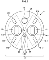
- Fig. 2 shows an example of a sealing plate.
- Fig. 3 shows the blocking mechanism 6 of the sealing plate and current collecting plates.
- Fig. 4 shows a sealing portion and a current collecting portion of the capacitor 2.
- Fig. 5 shows an arrangement form of the capacitor 2 and a blocking function for an electrolyte.
- the capacitor 2 includes a capacitor element 10, an exterior package case 12, a sealing plate 14, and current collecting plates 18-1, 18-2.
- the capacitor element 10 is impregnated with the electrolytic solution 4.
- the exterior package case 12 houses the electrolytic solution 4, the capacitor element 10, and the current collecting plates 18-1, 18-2 and is sealed by the sealing plate 14.
- the electrolytic solution 4 is an example of an electrolyte and has fluidity.
- the sealing plate 14 is provided with a safety valve 16 and this safety valve 16 is an example of a degassing valve and is also an example of a gas releasing mechanism.
- the sealing plate 14 is provided with first blocking walls 6-11, 6-12, 6-13, 6-14 and the current collecting plates 18-1, 18-2 are provided with second blocking walls 6-21, 6-22. Additionally, in this embodiment, the sealing plate 14 is provided with a third blocking wall 6-30.
- the blocking walls 6-11, 6-12, 6-13, 6-14, 6-21, 6-22, 6-30 are an example of the blocking mechanism 6 blocking the electrolytic solution 4 for the safety valve
- a of Fig. 1 shows a portion of the capacitor element 10.
- This capacitor element 10 is a winding element having respective electrode foils on the anode and cathode sides and a separator 48 overlapped and wound. This winding element is fixed by a fixing tape 50.
- the electrode foils for example, an aluminum foil is used as a base material, and polarizable electrodes containing an active material such as activated carbon, a binder, etc. are formed on the both surfaces of the aluminum foil.
- the capacitor element 10 has an element end surface 52 formed of an edge portion of the separator 48.
- electrode protruding portions 46-1, 46-2 on the anode side and the cathode side are formed by drawing out the edge portions of the electrode foils on the anode side and the cathode side.
- the electrode protruding portions 46-1, 46-2 are made up of a base member having aluminum surfaces exposed without forming the polarizable electrodes, and are formed of the edge portions of the electrode foils.
- each of the electrode protruding portions 46-1, 46-2 is formed into a fan shape having an angle of 120 degrees with a cut made in a circular arc portion at an angle of 40 degrees, for example, and is flattened by bending each portion toward the center of the element.
- the element end surface 52 has an insulation interval formed on the side of the facing surfaces of the electrode protruding portion 46-1 on the anode side and the electrode protruding portion 46-2 on the cathode side.
- This insulation interval includes a circular central part formed in the central part of the element end surface 52 of the capacitor element 10.
- FIG. B of Fig. 1 shows the current collecting plate 18-1 on the anode side.
- the current collecting plate 18-1 is connected to an external terminal 24-1 on the anode side.
- the current collecting plate 18-2 on the cathode side is the same as the current collecting plate 18-1 and is connected to the external terminal 24-2 on the cathode side.
- the current collecting plate 18-1 includes a main body portion 32.
- the main body portion 32 includes linear edge portions 34, 36 in crossing directions and includes a large-diameter circular arc portion 38 and a small-diameter circular arc portion 40 connecting the edge portions 34, 36.
- the circular arc portion 38 is disposed on the circumferential edge side of the capacitor element 10 and the circular arc portion 40 is disposed in the vicinity of the center of the capacitor element 10.
- One surface of the main body portion 32 has a triangular convex portion 70 formed with one vertex facing toward the circular arc portion 40 of the current collecting plates 18-1.
- One side of the convex portion 70 closer to the circular arc portion 38 acts as a current collecting plate connecting surface portion 71 connected to a terminal connecting surface portion 22 of the external terminal 24-1.
- Second blocking walls 6-21, 6-22 blocking the electrolytic solution 4 are disposed close to each of the edge portions 34, 36 of the current collecting plate 18-1.
- Each of the blocking walls 6-21, 6-22 is formed of a rectangular flat plate, for example.
- the second blocking walls 6-21, 6-22 are set equivalent to or lower than the height of a gap generated between the main body portion 32 and a rear surface of the sealing plate 14 (a surface facing the capacitor element 10) when the current collecting plate 18-1 is connected to the external terminal 24-1.
- the current collecting plate 18-2 on the cathode side has the same shape as the current collecting plate 18-1 on the anode side.
- Fig. 2 shows the rear surface of the sealing plate (the surface facing the capacitor element).
- the sealing plate 14 is an example of a sealing plate of the present invention.
- the sealing plate 14 is formed from a hard insulating synthetic resin, for example.
- the sealing plate 14 is provided with the external terminal 24-1 on the anode side, the external terminal 24-2 on the cathode side, the safety valve 16 acting as the gas releasing mechanism, a plurality of the first blocking walls 6-11, 6-12, 6-13, 6-14 blocking the electrolytic solution 4 (B of Fig. 5 ), and a third blocking wall 6-30.
- the first blocking walls 6-11, 6-12, 6-13, 6-14 are set equivalent to or lower than the height of a gap generated between the main body portion 32 and the rear surface of the sealing plate 14 (the surface facing the capacitor element 10) when the current collecting plates 18-1, 18-2 are connected to the external terminals 24-1, 24-2.
- the third blocking wall 6-30 is formed at a portion facing the insulation interval formed between the current collecting plates 18-1, 18-2 and is set to the same height as the first blocking walls 6-11, 6-12, 6-13, 6-14. Therefore, the current collecting plates 18-1, 18-2 do not exist on a surface facing the third blocking wall 6-30.
- Each of the external terminals 24-1, 24-2 is formed of a metal material with good conductivity and is attached to the sealing plate 14 by insert molding.
- the terminal connecting surface portion 22 is formed on each of the external terminals 24-1, 24-2.
- the terminal connecting surface portion 22 of the external terminal 24-1 is connected to the current collecting plate 18-1 on the anode side and the terminal connecting surface portion 22 of the external terminal 24-2 is connected to the current collecting plate 18-2 on the cathode side.
- the safety valve 16 is disposed in a valve hole portion 26 included in the sealing plate 14.
- the safety valve 16 includes, for example, a film portion having gas permeability and this film portion is disposed in the valve hole portion 26.
- the third blocking wall 6-30 is disposed in the vicinity of a center O of the sealing plate 14.
- the third blocking wall 6-30 is, by way of example, a triangle pole body erected in the perpendicular direction relative to the rear surface of the sealing plate 14.
- the third blocking wall 6-30 includes a surface portion 28 parallel to the edge portion of the current collecting plate 18-1 or the current collecting plate 18-2 and a surface portion 30 in a crossing direction relative to the surface portion 28.
- Each of the first blocking walls 6-11, 6-12, 6-13, 6-14 is a rectangular parallelepiped, by way of example.
- Each of the blocking walls 6-11, 6-12, 6-13, 6-14 is arranged in parallel with the edge portions of the current collecting plate 18-1 or the current collecting plate 18-2.
- Each of the current collecting plates 18-1, 18-2 is symmetrically arranged with the center O of the sealing plate 14, the safety valve 16, and the third blocking wall 6-30 interposed therebetween.
- the electrode protruding portions 46-1, 46-2 formed on the element end surface 52 of the capacitor element 10 are connected to the current collecting plates 18-1, 18-2.
- the current collecting plate 18-1 on the anode side and the current collecting plate 18-2 on the cathode side are placed on the electrode protruding portion 46-1 and the electrode protruding portion 46-2, respectively, such that the surfaces without the convex portions 70 are placed on the electrode protruding portions 46-1, 46-2.
- the current collecting plates 18-1, 18-2 are placed such that the circular arc portions 40 meets the central part of the element without contact between the current collecting plate 18-1 and the current collecting plate 18-2.
- the current collecting plates 18-1, 18-2 and the electrode protruding portions 46-1, 46-2 are welded by laser irradiation from the side of the current collecting plates 18-1, 18-2 to a portion of the main body portion 32 without the convex portion 70.
- This laser irradiation uses an inert gas such as argon gas and helium gas for a shielding gas to shield the capacitor element 10, thereby avoiding the effect of laser heat and sputtering on the capacitor element 10.
- the current collecting plates 18-1, 18-2 connected to the capacitor element 10 are connected to the external terminals 24-1, 24-2 formed on the sealing plate 14.
- the external terminals 24-1, 24-2 are placed such that the terminal connecting surface portions 22 thereof are linked to the current collecting plate connecting surface portions 71 of the convex portions 70 formed on the main body portions 32 of the current collecting plates 18-1, 18-2.
- the terminal connecting surface portions 22 are connected to the current collecting plate connecting surface portions 71 by irradiating the periphery of grounding portions of the terminal connecting surface portions 22 and the current collecting plate connecting surface portions 71 with a laser from the side of the circular arc portions 38 of the current collecting plates 18-1, 18-2.
- Fig. 3 shows the sealing plate 14 provided with the current collecting plates 18-1, 18-2 connected to the external terminals 24-1, 24-2.
- the sealing plate 14 and the current collecting plates 18-1, 18-2 form a space portion 54 ( Fig. 4 ) corresponding to the protrusion length of the external terminals 24-1, 24-2.
- the space formed by the space portion 54 and the insulation interval between the current collecting plate 18-1 and the current collecting plate 18-2 is a space that may act as a movement path of the electrolytic solution 4 when the electrolytic solution 4 splashes up.
- the first blocking walls 6-11, 6-12, 6-13, 6-14 and the third blocking wall 6-30 on the side of the sealing plate 14 and the second blocking walls 6-21, 6-22 described above on the side of the current collecting plates 18-1, 18-2 are arranged in this space.
- Fig. 4 shows a sealing portion of a capacitor.
- This capacitor 2 is an example of the capacitor of the present invention.
- the capacitor 2 includes the exterior package case 12 formed from an aluminum plate.
- the exterior package case 12 is a matter that a metal plate of aluminum etc is formed into a bottomed cylindrical shape, for example, and is formed into a circular shape, an elliptical shape, an oval shape, or a rectangular shape in accordance with the shape of the capacitor element 10 housed therein.
- the capacitor element 10 has a structure in which the electrode foils on the anode and cathode sides are laminated or wound via the separator 48 and is formed into a circular shape, an elliptical shape, an oval shape, or a rectangular shape.
- the exterior package case 12 has a cylindrical shape.
- the exterior package case 12 houses the capacitor element 10 and has the sealing plate 14 disposed on the opening portion side.
- the sealing plate 14 is disposed and positioned on a step portion 60 formed on the exterior package case 12, and an opening edge portion 64 of the exterior package case 12 subjected to a curling treatment is fixed to an elastic portion 62 disposed on the upper surface side of the sealing plate 14. As a result, the exterior package case 12 is sealed in a tight-seal state.
- Fig. 5 shows a state of the electrolytic solution 4 in the capacitor 2 when the capacitor 2 is disposed in a tilted manner.
- the electrolytic solution 4 enclosed in the exterior package case 12 and the electrolytic solution 4 contained in the capacitor element 10 move in a direction orthogonal to the gravity direction.
- the sealing plate 14 is on the lower side, the electrolytic solution 4 moving toward the sealing plate 14 is in contact with a portion of the sealing plate 14 as shown in B of Fig. 5 .
- the electrolytic solution 4 is blocked by the plurality of the blocking walls 6-11, 6-12, 6-13, 6-14, 6-30, 6-21, 6-22. Therefore, the electrolytic solution 4 does not touch the safety valve 16 and the electrolytic solution 4 does not enter the valve hole portion 26.
- the second blocking walls 6-21, 6-22 are arranged to surround the safety valve 16, thereby achieving a structure in which the electrolytic solution 4 hardly adheres to the safety valve 16.
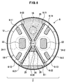
- Fig. 6 shows a capacitor including a trapezoidal (trapezium) electrolytic solution absorbent material.
- This capacitor 2 has an electrolytic solution absorbent material 8-1 disposed between the element end surface 52 and the sealing plate 14, avoiding the disposition positions of the current collecting plates 18-1, 18-2.
- the electrolytic solution absorbent material 8-1 is interposed and fixed between the edge portions 34, 36 and the second blocking walls 6-21, 6-22 of the current collecting plates 18-1, 18-2 and the third blocking wall 6-30.
- the electrolytic solution absorbent material 8-1 may be formed of a flexible spongy or porous body.
- the electrolytic solution absorbent material 8-1 absorbs and retains the surplus electrolytic solution 4 staying inside the exterior package case 12.
- the shape of the electrolytic solution absorbent material 8-1 is trapezoidal in the second embodiment, the shape is not limited to this, and the size and shape may be changed as needed depending on a desired absorbed amount of the electrolytic solution 4 and a size of the space between the current collecting plate 18-1 and the current collecting plate 18-2.
- the current collecting plates 18-1, 18-2 and the third blocking wall 6-30 are utilized as a means for fixing the electrolytic solution absorbent material 8-1, the means is not limited to this.
- the electrolytic solution absorbent material 8-1 may be interposed and fixed in the space portion 54 between the sealing plate 14 and the current collecting plates 18-1, 18-2 or may be fixed by using an adhesive.
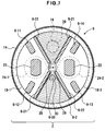
- Fig. 7 shows variation of another electrolytic solution absorbent material 8-1.
- This capacitor 2 has an electrolytic solution absorbent material 8-2 disposed in a surrounding manner on a peripheral edge of the sealing plate 14.
- This configuration allows the surrounding electrolytic solution absorbent material 8-2 to absorb and retain the surplus electrolytic solution 4 staying inside the exterior package case 12 regardless the arrangement direction of the capacitor 2 and, therefore, the electrolytic solution 4 can be prevented from adhering to the safety valve 16. Even if the electrolytic solution 4 splashes up due to vibrations, the electrolytic solution absorbent material 8-2 disposed on the peripheral edge can reduce the level of splashing-up.
- Fig. 8 shows the capacitor 2 including the electrolytic solution absorbent material 8-1.
- This electrolytic solution absorbent material 8-1 is disposed in an insulation interval 56 between the current collecting plates 18-1, 18-2 and is interposed and fixed at least between the facing portions of the element end surface 52 and the sealing plate 14.
- the electrolytic solution absorbent material 8-1 has one surface in contact with a portion of the sealing plate 14 facing toward the inside of the exterior package case 12 and the other surface side in contact with the element end surface 52 of the capacitor element 10.
- the first blocking walls 6-12, 6-13 formed on the sealing plate 14 are in contact with a portion of the facing surface side of the current collecting plates 18-1, 18-2, and the second blocking walls 6-21, 6-22 on the current collecting plates 18-1, 18-2 are disposed inside the first blocking walls 6-12, 6-13.
- the electrolytic solution absorbent material 8-1 is inserted in the insulation interval 56 between the current collecting plate 18-1 on the anode side and the current collecting plate 18-2 on the cathode side.
- a length L1 of the electrolytic solution absorbent material 8-1 is formed longer than a facing interval L2 between the element end surface 52 and the sealing plate 14 in the insulation interval 56.
- the length L1 of the electrolytic solution absorbent material 8-1 before disposition in the capacitor 2 is formed as a length twice longer than the facing interval L2, for example.
- the electrolytic solution absorbent material 8-1 is compressed by applying a predetermined compression force F in the up-down direction and inserted in the insulation interval 56.
- the electrolytic solution absorbent material 8-1 When inserted in the insulation interval 56, the electrolytic solution absorbent material 8-1 is disposed in a compressed state with a restoring force to the compression force F and is attached by pressure to the element end surface 52 and the sealing plate 14 to demonstrate the blocking function for the electrolytic solution 4.
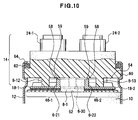
- the electrolytic solution absorbent material 8-1 may partially enter a gap 58 between the sealing plate 14 and the second blocking walls 6-21, 6-22 in accordance with restoration from the compression and may form a projection portion 59.
- the electrolytic solution absorbent material 8-1 is interposed and fixed between both the element end surface 52 and the second blocking walls 6-21, 6-22, which are end surfaces of the current collecting plates 18-1, 18-2, and the sealing plate 14.
- the projection portion 59 may be formed by a portion of the electrolytic solution absorbent material 8-1 entering inside the gap 58 depending on, for example, a horizontal length of formation of the electrolytic solution absorbent material 8-1 relative to the width of the insulation interval 56 and a ratio of the volume of the insulation interval 56 and the volume of the electrolytic solution absorbent material 8-1.
- the projection portion 59 has a different length entering inside the gap 58 depending on the hardness (viscosity) and the restoring characteristic of the electrolytic solution absorbent material 8-1.
- the capacitor 2 has the electrolytic solution absorbent material 8-1 disposed in the insulation interval 56 and the gap 58 and therefore can block the inflow of the electrolytic solution 4 to the safety valve 16.
- the electrolytic solution absorbent material 8-1 blocks the gap 58 between the blocking walls 6-21, 6-22 and the sealing plate 14 to prevent the surplus electrolytic solution 4 in the exterior package case 12 from flowing through the gap 58 toward the safety valve 16. Since the electrolytic solution absorbent material 8-1 is more firmly fixed by compression between the blocking walls 6-21, 6-22 and the sealing plate 14, the fixed state is maintained against impact and continuous vibrations on the capacitor element 2 and the blocking function for the electrolytic solution 4 can be maintained.
- This electrolytic solution absorbent material 8-1 can block the gap 58 between the blocking walls 6-21, 6-22 and the sealing plate 14 and can absorb the electrolytic solution 4 in the insulation interval 56 to prevent the inflow toward the safety valve 16.
- an interval may be formed between the first blocking walls 6-11, 6-12, 6-13, 6-14 on the sealing plate 14 and the current collecting plates 18-1, 18-2 and between the second blocking walls 6-21, 6-22 on the current collecting plates 18-1, 18-2 and the sealing plate 14, or these walls and plates may be arranged in close contact with each other.
- the height of the third blocking wall 6-30 on the sealing plate 14 is the same height as the other first blocking walls 6-11, 6-12, 6-13, 6-14 in the embodiments, the height is not limited to this. If the third blocking wall 6-30 is disposed at a position not facing the current collecting plates 18-1, 18-2 when the external terminals 24-1, 24-2 are connected to the current collecting plates 18-1, 18-2, the third blocking wall 6-30 may be extended to the element end surface 52 of the capacitor element 10. In this way, the path of the electrolytic solution 4 more closely passing through the center of the capacitor element 10 can be closed.
- the shape of the current collecting plates 18-1, 18-2 is the fan shape in the embodiments, the shape is not limited to this.
- the shape may be semicircular or the shapes of the current collecting plate 18-1 and the current collecting plate 18-2 may be different from each other.
- the surfaces of the convex portions 70 formed on the current collecting plates 18-1, 18-2 are utilized for the connection between the current collecting plates 18-1, 18-2 and the external terminals 24-1, 24-2, the connection is not limited to this.
- the main body portion 32 may partially be cut out on the side of the circular arc portion 38 to form a current collecting plate connecting surface portion or the main body portion 32 may have a bent shape to make a central part higher.
- first blocking walls 6-11, 6-12, 6-13, 6-14 are disposed inside the second blocking walls 6-21, 6-22 in the embodiments, a disposition of the first blocking walls 6-11, 6-12, 6-13, 6-14 is not limited to this.
- the first blocking walls 6-11, 6-12, 6-13, 6-14 and the second blocking walls 6-21, 6-22 are disposed at different positions. In particular, it is only necessary to avoid overlap between the first blocking walls 6-11, 6-12, 6-13, 6-14 and the second blocking walls 6-21, 6-22, and the second blocking walls 6-21, 6-22 may be disposed inside the first blocking walls 6-11, 6-12, 6-13, 6-14.
- electrode protruding portion 46-1 on the anode side and the electrode protruding portion 46-2 on the cathode side are formed on the one element end surface 52 of the capacitor element 10 in the embodiments, formations of the electrode protruding portions 46-1, 46-2 are not limited to this, and the electrode protruding portion on the anode side and the electrode protruding portion on the cathode side may be formed on different element end surfaces.
- the gas releasing mechanism is not limited to this.
- a through-hole may be formed in the sealing plate to dispose a gas permeable film such that the through-hole is closed, or the gas releasing mechanism may be a valve structure opening a tight-seal state when the internal pressure increases.
- this electrolyte includes such an electrolyte of which fluidity is increased by applying vibration etc. at the time of drive of the capacitor 2.
- the capacitor including the first, second, and third blocking walls as an example of the blocking mechanism 6 is exemplified in the embodiments, at least one of the first and second blocking walls may be included.
- the blocking mechanism 6 may be disposed on one or both of the sealing plate and the current collecting plate.
- a process of the electrolytic solution absorbent material 8-1 is not limited to this.
- the sealing plate 14 and the current collecting plates 18-1, 18-2 may be connected while the electrolytic solution absorbent material 8-1 is compressed.
- the gas releasing mechanism such as a safety valve is included in the sealing plate sealing the exterior package case enclosing the capacitor element, and the electrolyte staying in the exterior package case can be blocked from the gas releasing mechanism so as to prevent deterioration of the valve function of the gas releasing mechanism due to the electrolyte
- the invention of this disclosure can widely be utilized in capacitors such as electric double layer capacitors.
Landscapes
- Engineering & Computer Science (AREA)
- Power Engineering (AREA)
- Microelectronics & Electronic Packaging (AREA)
- Chemical & Material Sciences (AREA)
- Materials Engineering (AREA)
- Electric Double-Layer Capacitors Or The Like (AREA)
Abstract
Description
- A technique of this disclosure relates to a capacitor such as an electric double layer capacitor and an electrolytic capacitor.
- In a capacitor such as an electric double layer capacitor and an electrolytic capacitor, an electrolyte contained in a capacitor element stays in a case. Such a capacitor includes a gas releasing mechanism. This gas releasing mechanism discharges gas accumulated in an exterior package case at the time of drive of the capacitor. For this gas releasing mechanism, for example, a safety valve with gas permeability is used.
- Regarding a capacitor of this type, it is known that a Y-shaped projection is formed on a sealing plate to avoid contact of electrolytic solution leaking out at the time of operation of the safety valve with an external terminal by the projection on the sealing plate (e.g., Patent Literature 1).
- It is known that when a cap of a resign case is fused with a lower case by ultrasonic waves, electrolytic solution flowing out from a polarizable electrode due to vibrations is blocked by a blocking wall disposed on the cap to prevent the electrolytic solution from contaminating a fused portion (e.g., Patent Literature 2).
-
- Patent Literature 1:
Japanese Utility Model Application Laid-Open Publication No. 55-129447 - Patent Literature 2:
Japanese Laid-Open Patent Publication No. 2011-100998 - A capacitor including a gas releasing mechanism such as a safety valve on a sealing plate is normally mounted with the sealing plate located on the upper side. In such a mounting form, an electrolyte staying in an exterior package case moves toward a bottom portion of the exterior package case and is therefore kept away from the safety valve of the sealing plate, and the function of the gas releasing mechanism for the electrolyte is maintained.
- However, an electronic device having such a capacitor mounted thereon cannot necessarily maintain the ideal arrangement form described above for the capacitor and horizontal arrangement or tilt arrangement is inevitable depending on a mounting environment. Even when the gas releasing mechanism is away from the flowing electrolyte, the electrolyte adhering to a side surface of the exterior package case may splash up in a disposition environment accompanied by vibrations and may reduce the gas releasing function.
- A predetermined amount of electrolytic solution may be enclosed in the exterior package case so as to achieve a longer life of a capacitor. The electrolytic solution enclosed in the exterior package case flows inside the capacitor.
- If the electrolyte enters the gas releasing mechanism, a gas transmission path is blocked by the electrolyte. If the electrolyte adheres to a valve function portion, gas pressure is prevented from directly acting on the valve function portion. If the valve function portion is covered with the electrolyte, the valve function decreases due to deterioration in gas permeability etc., and an explosion-proof function is impaired due to a delay in valve opening in response to an abrupt increase in pressure etc.
-
Patent Literatures 1 and 2 do not disclose or suggest such a requirement and a problem and do not disclose or suggest a configuration etc. for solving the problem. - In view of the problem, it is therefore an object of the present invention to prevent deterioration in gas release function due to adherence of a flowing electrolyte.
- To achieved the object, an aspect of a capacitor of this disclosure provides a capacitor having an exterior package case housing an electrolyte along with a capacitor element, a sealing plate where an external terminal is disposed , the sealing plate sealing the exterior package case, and a current collecting plate disposed between an electrode protruding portion formed on an element end surface of the capacitor element and the external terminal, the capacitor comprising a gas releasing mechanism disposed in the sealing plate to release a gas in the exterior package case; and a blocking mechanism disposed on at least one of the sealing plate and the current collecting plate to block the electrolyte from the gas releasing mechanism.
- In this capacitor, preferably, the blocking mechanism may include a first blocking wall erected on the sealing plate to block the electrolyte, and a second blocking wall erected on the current collecting plate to block the electrolyte, and the second blocking wall may be provided for a position different from the first blocking wall.
- In this capacitor, preferably, the electrode protruding portion may be formed by protruding an electrode body on the anode side and an electrode body on the cathode side at different positions on one surface portion of the element end surface, and the current collecting plate on the anode side may be provided for the electrode protruding portion on the anode side and the current collecting plate on the cathode side may be provided for the electrode protruding portion on the cathode side.
- This capacitor may preferably comprise an insulation interval between the current collecting plate on the anode side and the current collecting plate on the cathode side, and a third blocking wall blocking the electrolyte in the insulation interval.
- This capacitor may preferably comprise an insulation interval at a position facing the gas releasing mechanism.
- This capacitor may preferably comprise an electrolyte absorbent material absorbing the electrolyte and blocking the electrolyte from the gas releasing mechanism.
- In this capacitor, preferably, the electrolyte absorbent material maybe disposed in an insulation interval formed between the current collecting plate on the anode side and the current collecting plate on the cathode side.
- In this capacitor, preferably, the electrolyte absorbent material may be interposed and fixed between an edge portion of the current collecting plate as well as the second blocking wall on the anode side and an edge portion of the current collecting plate as well as the second blocking wall on the cathode side.
- In this capacitor, preferably, the electrolyte absorbent material may be interposed and fixed between the element end surface and/or an end surface of the current collecting plate and the sealing plate.
- According to the capacitor of this disclosure, any of the following effects is provided.
-
- (1) Since the electrolyte splashing up due to, for example, vibrations applied to the capacitor is blocked by the blocking mechanism, the releasing function of the gas releasing mechanism is not reduced.
- (2) The electrolyte in motion such as flowing or splashing up can be blocked from the gas releasing mechanism even when the capacitor is arranged in the horizontal arrangement or the tilt arrangement or even when the capacitor is accompanied by vibrations regardless of an arrangement form so as to prevent function deterioration of the gas releasing mechanism due to adherence of electrolyte.
- (3) Since the function deterioration of the gas releasing mechanism can be prevented, the reliability of the capacitor is improved and the reliability can be maintained.
- Other objects, features, and advantages of the present invention will become more apparent by reference to the accompanying drawings and embodiments.
-
-
Fig. 1 is a perspective view of an example of a current collecting plate and a capacitor element of an electric double layer capacitor according to a first embodiment. -
Fig. 2 is a view of an example of a sealing plate of the electric double layer capacitor according to the first embodiment. -
Fig. 3 is a view of arrangement of blocking walls of the sealing plate and current collecting plates. -
Fig. 4 is a partial cross-sectional view of a sealing portion and a current collecting portion of the electric double layer capacitor. -
Fig. 5 is a view of a staying electrolytic solution and a blocking function for the electrolytic solution in tilt arrangement of the capacitor. -
Fig. 6 is a view of an electric double layer capacitor according to a second embodiment. -
Fig. 7 is a view of a variation of an electrolytic solution absorbent material. -
Fig. 8 is a partial cross-sectional view of an electric double layer capacitor according to a third embodiment. -
Fig. 9 is a view of an example of disposition of the electrolytic solution absorbent material to an insulation interval. -
Fig. 10 is a view of another example of a disposition state of the electrolytic solution absorbent material to an insulation interval. -
Fig. 11 is a view of a further example of a disposition state of the electrolytic solution absorbent material. - A capacitor of the present invention includes a
blocking mechanism 6 for anelectrolytic solution 4 for preventing deterioration of a gas releasing function due to flowing of theelectrolytic solution 4 contained in an electric double layer capacitor (hereinafter simply referred to as a "capacitor") 2 by way of example. Theelectrolytic solution 4 is an example of an electrolyte having fluidity. A first embodiment will be described in terms of an example of theblocking mechanism 6 and a second embodiment will be described in terms of the case that the capacitor is formed including first or second electrolytic solution absorbent material 8-1, 8-2 in addition to theblocking mechanism 6. The electrolytic solution absorbent material 8-1, 8-2 is an example of an electrolyte absorbent material. A third embodiment will be described in terms of a disposition state example of the electrolytic solution absorbent material 8-1, 8-2. - The first, second, and third embodiments will now be described with reference to examples shown in the figures.
-
Fig. 1 shows an example of a current collecting plate and a capacitor element of thecapacitor 2.Fig. 2 shows an example of a sealing plate.Fig. 3 shows theblocking mechanism 6 of the sealing plate and current collecting plates.Fig. 4 shows a sealing portion and a current collecting portion of thecapacitor 2.Fig. 5 shows an arrangement form of thecapacitor 2 and a blocking function for an electrolyte. - The
capacitor 2 includes acapacitor element 10, anexterior package case 12, a sealingplate 14, and current collecting plates 18-1, 18-2. Thecapacitor element 10 is impregnated with theelectrolytic solution 4. Theexterior package case 12 houses theelectrolytic solution 4, thecapacitor element 10, and the current collecting plates 18-1, 18-2 and is sealed by the sealingplate 14. Theelectrolytic solution 4 is an example of an electrolyte and has fluidity. The sealingplate 14 is provided with asafety valve 16 and thissafety valve 16 is an example of a degassing valve and is also an example of a gas releasing mechanism. The sealingplate 14 is provided with first blocking walls 6-11, 6-12, 6-13, 6-14 and the current collecting plates 18-1, 18-2 are provided with second blocking walls 6-21, 6-22. Additionally, in this embodiment, the sealingplate 14 is provided with a third blocking wall 6-30. The blocking walls 6-11, 6-12, 6-13, 6-14, 6-21, 6-22, 6-30 are an example of theblocking mechanism 6 blocking theelectrolytic solution 4 for thesafety valve 16. - A of
Fig. 1 shows a portion of thecapacitor element 10. Thiscapacitor element 10 is a winding element having respective electrode foils on the anode and cathode sides and aseparator 48 overlapped and wound. This winding element is fixed by a fixingtape 50. For the electrode foils, for example, an aluminum foil is used as a base material, and polarizable electrodes containing an active material such as activated carbon, a binder, etc. are formed on the both surfaces of the aluminum foil. Thecapacitor element 10 has anelement end surface 52 formed of an edge portion of theseparator 48. - On this
element end surface 52, electrode protruding portions 46-1, 46-2 on the anode side and the cathode side are formed by drawing out the edge portions of the electrode foils on the anode side and the cathode side. The electrode protruding portions 46-1, 46-2 are made up of a base member having aluminum surfaces exposed without forming the polarizable electrodes, and are formed of the edge portions of the electrode foils. In this embodiment, each of the electrode protruding portions 46-1, 46-2 is formed into a fan shape having an angle of 120 degrees with a cut made in a circular arc portion at an angle of 40 degrees, for example, and is flattened by bending each portion toward the center of the element. Theelement end surface 52 has an insulation interval formed on the side of the facing surfaces of the electrode protruding portion 46-1 on the anode side and the electrode protruding portion 46-2 on the cathode side. This insulation interval includes a circular central part formed in the central part of theelement end surface 52 of thecapacitor element 10. - B of
Fig. 1 shows the current collecting plate 18-1 on the anode side. The current collecting plate 18-1 is connected to an external terminal 24-1 on the anode side. The current collecting plate 18-2 on the cathode side is the same as the current collecting plate 18-1 and is connected to the external terminal 24-2 on the cathode side. - The current collecting plate 18-1 includes a
main body portion 32. Themain body portion 32 has a fan shape set to an opening angle θ=120 degrees. Themain body portion 32 includeslinear edge portions circular arc portion 38 and a small-diametercircular arc portion 40 connecting theedge portions circular arc portion 38 is disposed on the circumferential edge side of thecapacitor element 10 and thecircular arc portion 40 is disposed in the vicinity of the center of thecapacitor element 10. - One surface of the
main body portion 32 has a triangularconvex portion 70 formed with one vertex facing toward thecircular arc portion 40 of the current collecting plates 18-1. One side of theconvex portion 70 closer to thecircular arc portion 38 acts as a current collecting plate connectingsurface portion 71 connected to a terminal connectingsurface portion 22 of the external terminal 24-1. - Second blocking walls 6-21, 6-22 blocking the
electrolytic solution 4 are disposed close to each of theedge portions main body portion 32 and a rear surface of the sealing plate 14 (a surface facing the capacitor element 10) when the current collecting plate 18-1 is connected to the external terminal 24-1. - Although not shown, the current collecting plate 18-2 on the cathode side has the same shape as the current collecting plate 18-1 on the anode side.
-
Fig. 2 shows the rear surface of the sealing plate (the surface facing the capacitor element). The sealingplate 14 is an example of a sealing plate of the present invention. The sealingplate 14 is formed from a hard insulating synthetic resin, for example. The sealingplate 14 is provided with the external terminal 24-1 on the anode side, the external terminal 24-2 on the cathode side, thesafety valve 16 acting as the gas releasing mechanism, a plurality of the first blocking walls 6-11, 6-12, 6-13, 6-14 blocking the electrolytic solution 4 (B ofFig. 5 ), and a third blocking wall 6-30. The first blocking walls 6-11, 6-12, 6-13, 6-14 are set equivalent to or lower than the height of a gap generated between themain body portion 32 and the rear surface of the sealing plate 14 (the surface facing the capacitor element 10) when the current collecting plates 18-1, 18-2 are connected to the external terminals 24-1, 24-2. The third blocking wall 6-30 is formed at a portion facing the insulation interval formed between the current collecting plates 18-1, 18-2 and is set to the same height as the first blocking walls 6-11, 6-12, 6-13, 6-14. Therefore, the current collecting plates 18-1, 18-2 do not exist on a surface facing the third blocking wall 6-30. - Each of the external terminals 24-1, 24-2 is formed of a metal material with good conductivity and is attached to the sealing
plate 14 by insert molding. The terminal connectingsurface portion 22 is formed on each of the external terminals 24-1, 24-2. The terminal connectingsurface portion 22 of the external terminal 24-1 is connected to the current collecting plate 18-1 on the anode side and the terminal connectingsurface portion 22 of the external terminal 24-2 is connected to the current collecting plate 18-2 on the cathode side. - The
safety valve 16 is disposed in avalve hole portion 26 included in the sealingplate 14. Thesafety valve 16 includes, for example, a film portion having gas permeability and this film portion is disposed in thevalve hole portion 26. - The third blocking wall 6-30 is disposed in the vicinity of a center O of the sealing
plate 14. The third blocking wall 6-30 is, by way of example, a triangle pole body erected in the perpendicular direction relative to the rear surface of the sealingplate 14. The third blocking wall 6-30 includes asurface portion 28 parallel to the edge portion of the current collecting plate 18-1 or the current collecting plate 18-2 and asurface portion 30 in a crossing direction relative to thesurface portion 28. - Each of the first blocking walls 6-11, 6-12, 6-13, 6-14 is a rectangular parallelepiped, by way of example. Each of the blocking walls 6-11, 6-12, 6-13, 6-14 is arranged in parallel with the edge portions of the current collecting plate 18-1 or the current collecting plate 18-2.
- As indicated by broken lines, each of the current collecting plates 18-1, 18-2 is a fan-shaped circular arc plate having the opening angle θ=120 degrees, for example. Each of the current collecting plates 18-1, 18-2 is symmetrically arranged with the center O of the sealing
plate 14, thesafety valve 16, and the third blocking wall 6-30 interposed therebetween. - The electrode protruding portions 46-1, 46-2 formed on the
element end surface 52 of thecapacitor element 10 are connected to the current collecting plates 18-1, 18-2. The current collecting plate 18-1 on the anode side and the current collecting plate 18-2 on the cathode side are placed on the electrode protruding portion 46-1 and the electrode protruding portion 46-2, respectively, such that the surfaces without theconvex portions 70 are placed on the electrode protruding portions 46-1, 46-2. In this case, the current collecting plates 18-1, 18-2 are placed such that thecircular arc portions 40 meets the central part of the element without contact between the current collecting plate 18-1 and the current collecting plate 18-2. The current collecting plates 18-1, 18-2 and the electrode protruding portions 46-1, 46-2 are welded by laser irradiation from the side of the current collecting plates 18-1, 18-2 to a portion of themain body portion 32 without theconvex portion 70. This laser irradiation uses an inert gas such as argon gas and helium gas for a shielding gas to shield thecapacitor element 10, thereby avoiding the effect of laser heat and sputtering on thecapacitor element 10. - The current collecting plates 18-1, 18-2 connected to the
capacitor element 10 are connected to the external terminals 24-1, 24-2 formed on the sealingplate 14. The external terminals 24-1, 24-2 are placed such that the terminal connectingsurface portions 22 thereof are linked to the current collecting plate connectingsurface portions 71 of theconvex portions 70 formed on themain body portions 32 of the current collecting plates 18-1, 18-2. The terminal connectingsurface portions 22 are connected to the current collecting plate connectingsurface portions 71 by irradiating the periphery of grounding portions of the terminal connectingsurface portions 22 and the current collecting plate connectingsurface portions 71 with a laser from the side of thecircular arc portions 38 of the current collecting plates 18-1, 18-2. In this case, since themain body portions 32 are located between the current collecting plate connectingsurface portions 71 and thecircular arc portions 38, a sputter etc. generated by the laser irradiation are prevented from dropping onto theelement end surface 52 of thecapacitor element 10 to avoid a short circuit. -
Fig. 3 shows the sealingplate 14 provided with the current collecting plates 18-1, 18-2 connected to the external terminals 24-1, 24-2. - When the current collecting plates 18-1, 18-2 are connected to the external terminals 24-1, 24-2 of the sealing
plate 14, the sealingplate 14 and the current collecting plates 18-1, 18-2 form a space portion 54 (Fig. 4 ) corresponding to the protrusion length of the external terminals 24-1, 24-2. The space formed by thespace portion 54 and the insulation interval between the current collecting plate 18-1 and the current collecting plate 18-2 is a space that may act as a movement path of theelectrolytic solution 4 when theelectrolytic solution 4 splashes up. As indicated by broken lines, the first blocking walls 6-11, 6-12, 6-13, 6-14 and the third blocking wall 6-30 on the side of the sealingplate 14 and the second blocking walls 6-21, 6-22 described above on the side of the current collecting plates 18-1, 18-2 are arranged in this space. -
Fig. 4 shows a sealing portion of a capacitor. Thiscapacitor 2 is an example of the capacitor of the present invention. - The
capacitor 2 includes theexterior package case 12 formed from an aluminum plate. Theexterior package case 12 is a matter that a metal plate of aluminum etc is formed into a bottomed cylindrical shape, for example, and is formed into a circular shape, an elliptical shape, an oval shape, or a rectangular shape in accordance with the shape of thecapacitor element 10 housed therein. Thecapacitor element 10 has a structure in which the electrode foils on the anode and cathode sides are laminated or wound via theseparator 48 and is formed into a circular shape, an elliptical shape, an oval shape, or a rectangular shape. In the first embodiment, theexterior package case 12 has a cylindrical shape. - The
exterior package case 12 houses thecapacitor element 10 and has the sealingplate 14 disposed on the opening portion side. The sealingplate 14 is disposed and positioned on astep portion 60 formed on theexterior package case 12, and anopening edge portion 64 of theexterior package case 12 subjected to a curling treatment is fixed to anelastic portion 62 disposed on the upper surface side of the sealingplate 14. As a result, theexterior package case 12 is sealed in a tight-seal state. -
Fig. 5 shows a state of theelectrolytic solution 4 in thecapacitor 2 when thecapacitor 2 is disposed in a tilted manner. - When the
capacitor 2 is in the tilt arrangement at an angle θ, as shown in A ofFig. 5 , theelectrolytic solution 4 enclosed in theexterior package case 12 and theelectrolytic solution 4 contained in thecapacitor element 10 move in a direction orthogonal to the gravity direction. In this case, since the sealingplate 14 is on the lower side, theelectrolytic solution 4 moving toward the sealingplate 14 is in contact with a portion of the sealingplate 14 as shown in B ofFig. 5 . - In this case, a plurality of the blocking walls 6-11, 6-12, 6-13, 6-14, 6-21, 6-22, 6-30 is interposed between the
electrolytic solution 4 and thesafety valve 16. As a result, thesafety valve 16 is blocked from theelectrolytic solution 4. - In such a configuration, even when vibrations are applied to the
capacitor 2 and theelectrolytic solution 4 is shaken and splashed up, theelectrolytic solution 4 is blocked by the plurality of the blocking walls 6-11, 6-12, 6-13, 6-14, 6-30, 6-21, 6-22. Therefore, theelectrolytic solution 4 does not touch thesafety valve 16 and theelectrolytic solution 4 does not enter thevalve hole portion 26. The second blocking walls 6-21, 6-22 are arranged to surround thesafety valve 16, thereby achieving a structure in which theelectrolytic solution 4 hardly adheres to thesafety valve 16. -
- (1) The blocking walls 6-11, 6-12, 6-13, 6-14 are disposed on the sealing
plate 14 while the blocking walls 6-21, 6-22 are disposed on the current collecting plates 18-1, 18-2, and these blocking walls are arranged in a separated state. Thespace portion 54 between the sealingplate 14 and the current collecting plates 18-1, 18-2 does not prevent the conduction of gas and theelectrolytic solution 4 toward thesafety valve 16 is blocked by a plurality of the blocking walls 6-11, 6-12, 6-13, 6-14, the blocking wall 6-30, and the blocking walls 6-21, 6-22. As a result, theelectrolytic solution 4 adhering to the sealingplate 14 can be prevented from moving to thesafety valve 16. Even when thecapacitor 2 is horizontally placed or disposed with inclination and vibrations is applied to thecapacitor 2 so as to splash up theelectrolytic solution 4, theelectrolytic solution 4 can be prevented from reaching thesafety valve 16. - (2) Even if a gap is generated between the lower end surfaces of the blocking walls 6-11, 6-12, 6-13, 6-14 and the
main body portions 32 of the current collecting plates 18-1, 18-2 as well as between the upper end surfaces of the blocking walls 6-21, 6-22 and the rear surface of the sealingplate 14, the blocking walls 6-11, 6-12, 6-13, 6-14 and the blocking walls 6-21, 6-22 are disposed in parallel arrangement and theelectrolytic solution 4 can thereby be prevented from entering from the gap. In particular, even if a gap is generated between the upper end surfaces of the blocking walls 6-21, 6-22 and the rear surface of the sealingplate 14 and theelectrolytic solution 4 enters from the gap, the blocking walls 6-11, 6-12, 6-13, 6-14 are formed toward themain body portions 32 of the current collecting plates 18-1, 18-2 to face the gap. Therefore, even when a gap is generated between the blocking walls 6-21, 6-22 and the sealingplate 14 and theelectrolytic solution 4 passes through the gap, the movement of theelectrolytic solution 4 toward thesafety valve 16 can be restrained by the blocking walls 6-11, 6-12, 6-13, 6-14 facing the gap. - (3) The blocking wall 6-30 is disposed to close the movement path of the
electrolytic solution 4 to thesafety valve 16, the movement path including the space formed with the insulating interval between the current collecting plate 18-1 and the current collecting plate 18-2. Therefore, even if thecapacitor 2 is disposed in a tilted manner with the sealingplate 14 located on the lower side and thesafety valve 16 located on the upper side and theelectrolytic solution 4 collected on the side opposite to thesafety valve 16 splashes up toward thesafety valve 16 due to vibrations, adherence to thesafety valve 16 side can be avoided. In particular, theelectrolytic solution 4 can be prevented by the blocking wall 6-30 from entering in the space formed with the insulating interval between the current collecting plate 18-1 and the current collecting plate 18-2. - (4) Since the
electrolytic solution 4 does not adhere to thesafety valve 16, the valve function of thesafety valve 16 is not impaired. The gas discharge function and the explosion-proof function are maintained and the reliability of thecapacitor 2 is retained. - (5) As shown in
Fig. 3 , the current collecting plates 18-1, 18-2 are formed into a fan shape and are disposed without covering thesafety valve 16. In particular, the insulation interval is included at a position facing thesafety valve 16 that is an example of the gas releasing mechanism and the current collecting plates 18-1, 18-2 do not exist at a position under thesafety valve 16. Therefore, the current collecting plates 18-1, 18-2 are not interposed between theelement end surface 52 of thecapacitor element 10 and thesafety valve 16 and theelectrolytic solution 4 can be prevented from staying and moving through the mediation of the current collecting plates 18-1, 18-2. The function of thesafety valve 16 can be prevented from deteriorating due to theelectrolytic solution 4. In particular, theelectrolytic solution 4 is prevented from being guided through the current collecting plates 18-1, 18-2 to thesafety valve 16. -
Fig. 6 shows a capacitor including a trapezoidal (trapezium) electrolytic solution absorbent material. Thiscapacitor 2 has an electrolytic solution absorbent material 8-1 disposed between theelement end surface 52 and the sealingplate 14, avoiding the disposition positions of the current collecting plates 18-1, 18-2. The electrolytic solution absorbent material 8-1 is interposed and fixed between theedge portions electrolytic solution 4 staying inside theexterior package case 12. - Although the shape of the electrolytic solution absorbent material 8-1 is trapezoidal in the second embodiment, the shape is not limited to this, and the size and shape may be changed as needed depending on a desired absorbed amount of the
electrolytic solution 4 and a size of the space between the current collecting plate 18-1 and the current collecting plate 18-2. - Although the current collecting plates 18-1, 18-2 and the third blocking wall 6-30 are utilized as a means for fixing the electrolytic solution absorbent material 8-1, the means is not limited to this. For example, the electrolytic solution absorbent material 8-1 may be interposed and fixed in the
space portion 54 between the sealingplate 14 and the current collecting plates 18-1, 18-2 or may be fixed by using an adhesive. -
Fig. 7 shows variation of another electrolytic solution absorbent material 8-1. Thiscapacitor 2 has an electrolytic solution absorbent material 8-2 disposed in a surrounding manner on a peripheral edge of the sealingplate 14. - This configuration allows the surrounding electrolytic solution absorbent material 8-2 to absorb and retain the surplus
electrolytic solution 4 staying inside theexterior package case 12 regardless the arrangement direction of thecapacitor 2 and, therefore, theelectrolytic solution 4 can be prevented from adhering to thesafety valve 16. Even if theelectrolytic solution 4 splashes up due to vibrations, the electrolytic solution absorbent material 8-2 disposed on the peripheral edge can reduce the level of splashing-up. -
- (1) Since the
electrolytic solution 4 collected in theexterior package case 12 is absorbed by the electrolytic solution absorbent material 8-1 or the electrolytic solution absorbent material 8-2, an amount of the splashing-upelectrolytic solution 4 can be reduced as far as possible. - (2) If the
capacitor 2 is disposed in the tilt arrangement (e. g. , A ofFig. 5 ), the electrolytic solution absorbent material 8-1 can be disposed at a lower part in which theelectrolytic solution 4 accumulates, so as to retain theelectrolytic solution 4 in the electrolytic solution absorbent material 8-1 and to prevent theelectrolytic solution 4 from splashing up. As a result theelectrolytic solution 4 to thesafety valve 16 can be blocked. - (3) The electrolytic solution absorbent material 8-2 can be disposed in a surrounding manner on the inner wall of the
exterior package case 12 so as to absorb and retain theelectrolytic solution 4 in the electrolytic solution absorbent material 8-2. Therefore, theelectrolytic solution 4 can be blocked from thesafety valve 16 even when thecapacitor 2 is in the horizontal arrangement or the tilt arrangement or the arrangement with thesafety valve 16 located on the lower side etc. -
Fig. 8 shows thecapacitor 2 including the electrolytic solution absorbent material 8-1. This electrolytic solution absorbent material 8-1 is disposed in aninsulation interval 56 between the current collecting plates 18-1, 18-2 and is interposed and fixed at least between the facing portions of theelement end surface 52 and the sealingplate 14. In particular, the electrolytic solution absorbent material 8-1 has one surface in contact with a portion of the sealingplate 14 facing toward the inside of theexterior package case 12 and the other surface side in contact with theelement end surface 52 of thecapacitor element 10. - In the
capacitor 2, for example, as depicted in A ofFig. 9 , the first blocking walls 6-12, 6-13 formed on the sealingplate 14 are in contact with a portion of the facing surface side of the current collecting plates 18-1, 18-2, and the second blocking walls 6-21, 6-22 on the current collecting plates 18-1, 18-2 are disposed inside the first blocking walls 6-12, 6-13. For example, as depicted in B of theFig. 9 , the electrolytic solution absorbent material 8-1 is inserted in theinsulation interval 56 between the current collecting plate 18-1 on the anode side and the current collecting plate 18-2 on the cathode side. - A length L1 of the electrolytic solution absorbent material 8-1 is formed longer than a facing interval L2 between the
element end surface 52 and the sealingplate 14 in theinsulation interval 56. The length L1 of the electrolytic solution absorbent material 8-1 before disposition in thecapacitor 2 is formed as a length twice longer than the facing interval L2, for example. - For example, the electrolytic solution absorbent material 8-1 is compressed by applying a predetermined compression force F in the up-down direction and inserted in the
insulation interval 56. When inserted in theinsulation interval 56, the electrolytic solution absorbent material 8-1 is disposed in a compressed state with a restoring force to the compression force F and is attached by pressure to theelement end surface 52 and the sealingplate 14 to demonstrate the blocking function for theelectrolytic solution 4. - For example, as depicted in
Fig. 10 , the electrolytic solution absorbent material 8-1 may partially enter agap 58 between the sealingplate 14 and the second blocking walls 6-21, 6-22 in accordance with restoration from the compression and may form aprojection portion 59. In this case, the electrolytic solution absorbent material 8-1 is interposed and fixed between both theelement end surface 52 and the second blocking walls 6-21, 6-22, which are end surfaces of the current collecting plates 18-1, 18-2, and the sealingplate 14. - The
projection portion 59 may be formed by a portion of the electrolytic solution absorbent material 8-1 entering inside thegap 58 depending on, for example, a horizontal length of formation of the electrolytic solution absorbent material 8-1 relative to the width of theinsulation interval 56 and a ratio of the volume of theinsulation interval 56 and the volume of the electrolytic solution absorbent material 8-1. Theprojection portion 59 has a different length entering inside thegap 58 depending on the hardness (viscosity) and the restoring characteristic of the electrolytic solution absorbent material 8-1. If theprojection portion 59 is formed, side surface portions of the electrolytic solution absorbent material 8-1 is, for example, supported along the edge portions 34 (36) and the blocking walls 6-21, 6-22 of the current collecting plates 18-1, 18-2 and theprojection portion 59 is engaged with thegap 58. As a result, the electrolytic solution absorbent material 8-1 is firmly fixed in theinsulation interval 56. - Therefore, the
capacitor 2 has the electrolytic solution absorbent material 8-1 disposed in theinsulation interval 56 and thegap 58 and therefore can block the inflow of theelectrolytic solution 4 to thesafety valve 16. -
- (1) The electrolytic solution absorbent material 8-1 may be inserted in a compressed state only in the
gap 58 between the sealingplate 14 and both the blocking wall 6-21 on the current collecting plate 18-1 and the blocking wall 6-22 on the current collecting plate 18-2. Therefore, for example, as depicted inFig. 11 , thecapacitor 2 may include the electrolytic solution absorbent material 8-1 inserted between both the blocking wall 6-21 on the current collecting plate 18-1 and the blocking wall 6-22 on the current collecting plate 18-2 and the sealingplate 14. This electrolytic solution absorbent material 8-1 is disposed along the end surfaces of the blocking walls 6-21, 6-22. The electrolytic solution absorbent material 8-1 is formed longer than the height of thegap 58 and may be compressed and inserted into thegap 58. The electrolytic solution absorbent material 8-1 is interposed and fixed between the blocking walls 6-21, 6-22, which are the end surfaces of the current collecting plates 18-1, 18-2, and the sealingplate 14. - As a result, the electrolytic solution absorbent material 8-1 blocks the
gap 58 between the blocking walls 6-21, 6-22 and the sealingplate 14 to prevent the surpluselectrolytic solution 4 in theexterior package case 12 from flowing through thegap 58 toward thesafety valve 16. Since the electrolytic solution absorbent material 8-1 is more firmly fixed by compression between the blocking walls 6-21, 6-22 and the sealingplate 14, the fixed state is maintained against impact and continuous vibrations on thecapacitor element 2 and the blocking function for theelectrolytic solution 4 can be maintained. -
- (2) The inserted electrolytic solution absorbent material 8-1 of the
capacitor 2 may be fixed in a compressed state at least in thegap 58 between the sealingplate 14 and both the blocking wall 6-21 of the current collecting plate 18-1 and the blocking wall 6-22 of the current collecting plate 18-2. This electrolytic solution absorbent material 8-1 is not limited to those having a quadrangular cross-sectional shape, for example, and may partially form a portion disposed between the blocking walls 6-21, 6-22 and the sealingplate 14, and the thickness of the portion may be formed longer than the height of thegap 58. In this case, the thickness of the portion of the electrolytic solution absorbent material 8-1 disposed in theinsulation interval 56 may be, for example, formed equivalent to or smaller than the interval between theelement end surface 52 and the sealingplate 14. - This electrolytic solution absorbent material 8-1 can block the
gap 58 between the blocking walls 6-21, 6-22 and the sealingplate 14 and can absorb theelectrolytic solution 4 in theinsulation interval 56 to prevent the inflow toward thesafety valve 16. -
- (3) Regarding the electrolytic solution absorbent material 8-2 depicted in
Fig. 7 , the electrolytic solution absorbent material 8-2 having a thickness longer than the interval between the sealingplate 14 and theelement end surface 52 of thecapacitor element 10 may be inserted in a compressed state in the same way. -
- (1) Since the electrolytic solution absorbent material 8-1, 8-2 is attached by pressure and firmly fixed to the
element end surface 52 and the sealingplate 14, the fixed state is maintained against impact and continuous vibrations on thecapacitor element 2 and the blocking function through absorption of theelectrolytic solution 4 can be maintained. - (2) Since the electrolytic solution absorbent material 8-1 is compressed and inserted to close the
gap 58 between the second blocking walls 6-21, 6-22 and the sealingplate 14, the electrolytic solution absorbent material 8-1 can retain theelectrolytic solution 4 and can prevent the splashing-up etc. of theelectrolytic solution 4 to block the inflow of theelectrolytic solution 4 to thesafety valve 16. - In the embodiments, an interval may be formed between the first blocking walls 6-11, 6-12, 6-13, 6-14 on the sealing
plate 14 and the current collecting plates 18-1, 18-2 and between the second blocking walls 6-21, 6-22 on the current collecting plates 18-1, 18-2 and the sealingplate 14, or these walls and plates may be arranged in close contact with each other. - Although the height of the third blocking wall 6-30 on the sealing
plate 14 is the same height as the other first blocking walls 6-11, 6-12, 6-13, 6-14 in the embodiments, the height is not limited to this. If the third blocking wall 6-30 is disposed at a position not facing the current collecting plates 18-1, 18-2 when the external terminals 24-1, 24-2 are connected to the current collecting plates 18-1, 18-2, the third blocking wall 6-30 may be extended to theelement end surface 52 of thecapacitor element 10. In this way, the path of theelectrolytic solution 4 more closely passing through the center of thecapacitor element 10 can be closed. - Although the shape of the current collecting plates 18-1, 18-2 is the fan shape in the embodiments, the shape is not limited to this. The shape may be semicircular or the shapes of the current collecting plate 18-1 and the current collecting plate 18-2 may be different from each other.
- Although the surfaces of the
convex portions 70 formed on the current collecting plates 18-1, 18-2 are utilized for the connection between the current collecting plates 18-1, 18-2 and the external terminals 24-1, 24-2, the connection is not limited to this. For example, themain body portion 32 may partially be cut out on the side of thecircular arc portion 38 to form a current collecting plate connecting surface portion or themain body portion 32 may have a bent shape to make a central part higher. - Although the first blocking walls 6-11, 6-12, 6-13, 6-14 are disposed inside the second blocking walls 6-21, 6-22 in the embodiments, a disposition of the first blocking walls 6-11, 6-12, 6-13, 6-14 is not limited to this. The first blocking walls 6-11, 6-12, 6-13, 6-14 and the second blocking walls 6-21, 6-22 are disposed at different positions. In particular, it is only necessary to avoid overlap between the first blocking walls 6-11, 6-12, 6-13, 6-14 and the second blocking walls 6-21, 6-22, and the second blocking walls 6-21, 6-22 may be disposed inside the first blocking walls 6-11, 6-12, 6-13, 6-14.
- Although the electrode protruding portion 46-1 on the anode side and the electrode protruding portion 46-2 on the cathode side are formed on the one
element end surface 52 of thecapacitor element 10 in the embodiments, formations of the electrode protruding portions 46-1, 46-2 are not limited to this, and the electrode protruding portion on the anode side and the electrode protruding portion on the cathode side may be formed on different element end surfaces. - Although the
safety valve 16 is used as the gas releasing mechanism in the embodiments, the gas releasing mechanism is not limited to this. For example, a through-hole may be formed in the sealing plate to dispose a gas permeable film such that the through-hole is closed, or the gas releasing mechanism may be a valve structure opening a tight-seal state when the internal pressure increases. - Although the
electrolytic solution 4 having fluidity is exemplified as an example of an electrolyte in the embodiments, this electrolyte includes such an electrolyte of which fluidity is increased by applying vibration etc. at the time of drive of thecapacitor 2. - Although the capacitor including the first, second, and third blocking walls as an example of the
blocking mechanism 6 is exemplified in the embodiments, at least one of the first and second blocking walls may be included. Theblocking mechanism 6 may be disposed on one or both of the sealing plate and the current collecting plate. - Although the long and large electrolytic solution absorbent material 8-1 is compressed and inserted between the current collecting plates 18-1, 18-2 and the sealing
plate 14 in the case described in the embodiments, a process of the electrolytic solution absorbent material 8-1 is not limited to this. In a manufacturing process of thecapacitor 2, for example, after the electrolytic solution absorbent material 8-1 is disposed on theelement end surface 52, the sealingplate 14 and the current collecting plates 18-1, 18-2 may be connected while the electrolytic solution absorbent material 8-1 is compressed. - As described above, the most preferable embodiments etc. of the invention of this disclosure have been described. The invention of this disclosure is not limited by the above description and explanation. On the basis of the spirit of the invention described in claims or the spirit of the invention disclosed in the description of embodiments, various modifications and alterations can be made by those skilled in that art and these modifications and alterations obviously fall within the scope of the present invention.
- Since the gas releasing mechanism such as a safety valve is included in the sealing plate sealing the exterior package case enclosing the capacitor element, and the electrolyte staying in the exterior package case can be blocked from the gas releasing mechanism so as to prevent deterioration of the valve function of the gas releasing mechanism due to the electrolyte, the invention of this disclosure can widely be utilized in capacitors such as electric double layer capacitors.
-
- 2 electric double layer capacitor
- 4 electrolytic solution
- 6 blocking mechanism
- 6-11, 6-12, 6-13, 6-14 first blocking wall
- 6-21, 6-22 second blocking wall
- 6-30 third blocking wall
- 8-1 electrolytic solution absorbent material
- 8-2 electrolytic solution absorbent material
- 10 capacitor element
- 12 exterior package case
- 14 sealing plate
- 16 safety valve
- 18-1, 18-2 current collecting plate
- 22 terminal connecting surface portion
- 24-1, 24-2 external terminal
- 26 valve hole portion
- 28 surface portion
- 30 surface portion
- 32 main body portion
- 34 edge portion
- 36 edge portion
- 38 circular arc portion
- 40 circular arc portion
- 46-1, 46-2 electrode protruding portion
- 48 separator
- 50 fixing tape
- 52 element end surface
- 54 space portion
- 56 insulation interval
- 58 gap
- 59 projection portion
- 60 step portion
- 62 elastic portion
- 64 opening edge portion
- 70 convex portion
- 71 current collecting plate connecting surface portion
Claims (9)
- A capacitor having an exterior package case housing an electrolyte along with a capacitor element, a sealing plate where an external terminal is disposed, the sealing plate sealing the exterior package case, and a current collecting plate disposed between an electrode protruding portion formed on an element end surface of the capacitor element and the external terminal, the capacitor comprising:a gas releasing mechanism disposed in the sealing plate to release a gas in the exterior package case; anda blocking mechanism disposed on at least one of the sealing plate and the current collecting plate to block the electrolyte from the gas releasing mechanism.
- The capacitor according to claim 1, wherein
the blocking mechanism includes
a first blocking wall erected on the sealing plate to block the electrolyte, and
a second blocking wall erected on the current collecting plate to block the electrolyte, and wherein
the second blocking wall is provided for a position different from the first blocking wall. - The capacitor according to claim 1 or claim 2,
wherein
the electrode protruding portion is formed by protruding an electrode body on the anode side and an electrode body on the cathode side at different positions on one surface portion of the element end surface, and wherein
the current collecting plate on the anode side is provided for the electrode protruding portion on the anode side and the current collecting plate on the cathode side is provided for the electrode protruding portion on the cathode side. - The capacitor according to claim 3, the capacitor comprising an insulation interval between the current collecting plate on the anode side and the current collecting plate on the cathode side, and a third blocking wall blocking the electrolyte in the insulation interval.
- The capacitor according to any one of claims 1 to 4, the capacitor comprising an insulation interval at a position facing the gas releasing mechanism.
- The capacitor according to any one of claims 1 to 5, the capacitor comprising an electrolyte absorbent material absorbing the electrolyte and blocking the electrolyte from the gas releasing mechanism.
- The capacitor according to claim 6, wherein the electrolyte absorbent material is disposed in an insulation interval formed between the current collecting plate on the anode side and the current collecting plate on the cathode side.
- The capacitor according to claim 7, wherein the electrolyte absorbent material is interposed and fixed between an edge portion of the current collecting plate as well as the second blocking wall on the anode side and an edge portion of the current collecting plate as well as the second blocking wall on the cathode side.
- The capacitor according to any one of claims 6 to 8, wherein the electrolyte absorbent material is interposed and fixed between the element end surface and/or an end surface of the current collecting plate and the sealing plate.
Applications Claiming Priority (2)
| Application Number | Priority Date | Filing Date | Title |
|---|---|---|---|
| JP2013125626 | 2013-06-14 | ||
| PCT/JP2014/003128 WO2014199639A1 (en) | 2013-06-14 | 2014-06-12 | Capacitor |
Publications (3)
| Publication Number | Publication Date |
|---|---|
| EP3010029A1 true EP3010029A1 (en) | 2016-04-20 |
| EP3010029A4 EP3010029A4 (en) | 2017-04-26 |
| EP3010029B1 EP3010029B1 (en) | 2021-01-06 |
Family
ID=52021951
Family Applications (1)
| Application Number | Title | Priority Date | Filing Date |
|---|---|---|---|
| EP14811742.7A Not-in-force EP3010029B1 (en) | 2013-06-14 | 2014-06-12 | Capacitor with gas release mechanism |
Country Status (5)
| Country | Link |
|---|---|
| US (1) | US9875856B2 (en) |
| EP (1) | EP3010029B1 (en) |
| JP (1) | JP6493205B2 (en) |
| CN (1) | CN105308699B (en) |
| WO (1) | WO2014199639A1 (en) |
Families Citing this family (10)
| Publication number | Priority date | Publication date | Assignee | Title |
|---|---|---|---|---|
| TWI546836B (en) * | 2014-10-28 | 2016-08-21 | 鈺邦科技股份有限公司 | Opening-sealed element and solid electrolytic capacitor thereof |
| KR102096430B1 (en) * | 2015-01-15 | 2020-04-02 | 엘에스엠트론 주식회사 | External terminal member of electric energy storage device having structure for preventing electrolyte leakage |
| JP7034577B2 (en) * | 2015-03-06 | 2022-03-14 | 日東電工株式会社 | Hydrogen discharge membrane |
| JP6972854B2 (en) * | 2016-09-28 | 2021-11-24 | 日本ケミコン株式会社 | Capacitors and their manufacturing methods |
| DE102018127263A1 (en) * | 2018-10-31 | 2020-04-30 | Tdk Electronics Ag | capacitor |
| DE102019133565A1 (en) * | 2019-12-09 | 2021-06-10 | Tdk Electronics Ag | Electrolytic capacitor with control element for gas diffusion |
| JP7806443B2 (en) * | 2021-11-02 | 2026-01-27 | 日本ケミコン株式会社 | Electricity storage device and method for manufacturing the same |
| CN115117565A (en) * | 2022-08-12 | 2022-09-27 | 楚能新能源股份有限公司 | Converge subassembly and cylinder battery |
| CN117174491B (en) * | 2023-10-16 | 2024-01-26 | 东莞市爱伦电子科技有限公司 | Electrolytic capacitor |
| CN121366811B (en) * | 2025-12-17 | 2026-05-08 | 东莞市爱伦电子科技有限公司 | A type of ultra-low temperature horn capacitor |
Family Cites Families (10)
| Publication number | Priority date | Publication date | Assignee | Title |
|---|---|---|---|---|
| JPS55129447U (en) | 1979-03-08 | 1980-09-12 | ||
| JP2004022233A (en) * | 2002-06-13 | 2004-01-22 | Tookan:Kk | Battery with danger prevention mechanism |
| JP2004071266A (en) * | 2002-08-05 | 2004-03-04 | Sanyo Electric Co Ltd | Non-aqueous electrolyte secondary battery and method of manufacturing the same |
| KR100599803B1 (en) * | 2004-09-24 | 2006-07-12 | 삼성에스디아이 주식회사 | Secondary Battery, Electrode Assembly and Current Collecting Plate Used in the Same |
| EP2075809A4 (en) * | 2006-10-16 | 2014-09-17 | Panasonic Corp | CONDENSER |
| US20110102972A1 (en) | 2009-11-05 | 2011-05-05 | Samsung Elctro-Mechanics Co., Ltd. | Chip-type electric double layer capacitor cell and method of manufacturing the same |
| JP5581934B2 (en) * | 2010-09-22 | 2014-09-03 | 日本ケミコン株式会社 | Electrolytic capacitor |
| JP5961939B2 (en) * | 2011-07-21 | 2016-08-03 | 日本ケミコン株式会社 | Capacitor manufacturing method |
| JP5961940B2 (en) * | 2011-07-21 | 2016-08-03 | 日本ケミコン株式会社 | Capacitor manufacturing method |
| CN103210459B (en) | 2010-11-09 | 2016-08-10 | 日本贵弥功株式会社 | Capacitor and its manufacturing method |
-
2014
- 2014-06-12 WO PCT/JP2014/003128 patent/WO2014199639A1/en not_active Ceased
- 2014-06-12 EP EP14811742.7A patent/EP3010029B1/en not_active Not-in-force
- 2014-06-12 JP JP2015522549A patent/JP6493205B2/en active Active
- 2014-06-12 CN CN201480032071.8A patent/CN105308699B/en active Active
-
2015
- 2015-12-08 US US14/962,771 patent/US9875856B2/en not_active Expired - Fee Related
Also Published As
| Publication number | Publication date |
|---|---|
| CN105308699A (en) | 2016-02-03 |
| WO2014199639A1 (en) | 2014-12-18 |
| JPWO2014199639A1 (en) | 2017-02-23 |
| US9875856B2 (en) | 2018-01-23 |
| CN105308699B (en) | 2018-04-06 |
| EP3010029A4 (en) | 2017-04-26 |
| US20160093450A1 (en) | 2016-03-31 |
| EP3010029B1 (en) | 2021-01-06 |
| JP6493205B2 (en) | 2019-04-03 |
Similar Documents
| Publication | Publication Date | Title |
|---|---|---|
| EP3010029B1 (en) | Capacitor with gas release mechanism | |
| US8603667B1 (en) | Electrochemical device | |
| JP5849623B2 (en) | Electricity storage element | |
| JP5672863B2 (en) | battery | |
| JPWO2017056742A1 (en) | Power storage device and method for manufacturing power storage device | |
| JP6079338B2 (en) | Power storage device and method for manufacturing power storage device | |
| JP6015582B2 (en) | Electricity storage element | |
| US7031140B2 (en) | Electric double layer capacitor, electrolytic cell and process for fabricating same | |
| JP5779387B2 (en) | Electrochemical devices | |
| JP5728263B2 (en) | Electrochemical devices | |
| JP6346449B2 (en) | Secondary battery | |
| JP2012033396A (en) | Rectangular secondary battery | |
| JP2014220197A (en) | Power storage element and method of manufacturing power storage element | |
| JP7095293B2 (en) | Power storage element | |
| JP2015022941A (en) | Power storage element | |
| JP2005166974A (en) | Electric double layer capacitor, electrolyte battery, and manufacturing method thereof | |
| JP6645533B2 (en) | Storage element | |
| WO2015133340A1 (en) | Electrochemical device | |
| JP6064878B2 (en) | Power storage module | |
| JP2012204002A (en) | Power storage device | |
| KR101297093B1 (en) | Wiring substrate and super capacitor of surface mount type using the same | |
| JP5875129B2 (en) | Electrochemical devices | |
| JP7771999B2 (en) | Energy storage cell | |
| KR101549812B1 (en) | Ceramic substrate and super capacitor of surface mount type using the same | |
| JP2025078345A (en) | Water capture member and non-aqueous electrolyte device |
Legal Events
| Date | Code | Title | Description |
|---|---|---|---|
| PUAI | Public reference made under article 153(3) epc to a published international application that has entered the european phase |
Free format text: ORIGINAL CODE: 0009012 |
|
| 17P | Request for examination filed |
Effective date: 20151222 |
|
| AK | Designated contracting states |
Kind code of ref document: A1 Designated state(s): AL AT BE BG CH CY CZ DE DK EE ES FI FR GB GR HR HU IE IS IT LI LT LU LV MC MK MT NL NO PL PT RO RS SE SI SK SM TR |
|
| AX | Request for extension of the european patent |
Extension state: BA ME |
|
| R17P | Request for examination filed (corrected) |
Effective date: 20151222 |
|
| DAX | Request for extension of the european patent (deleted) | ||
| A4 | Supplementary search report drawn up and despatched |
Effective date: 20170309 |
|
| RIC1 | Information provided on ipc code assigned before grant |
Ipc: H01G 11/74 20130101ALI20170303BHEP Ipc: H01G 11/80 20130101ALI20170303BHEP Ipc: H01G 11/14 20130101ALI20170303BHEP Ipc: H01G 11/18 20130101ALI20170303BHEP Ipc: H01G 9/12 20060101AFI20170303BHEP |
|
| RA4 | Supplementary search report drawn up and despatched (corrected) |
Effective date: 20170322 |
|
| STAA | Information on the status of an ep patent application or granted ep patent |
Free format text: STATUS: EXAMINATION IS IN PROGRESS |
|
| 17Q | First examination report despatched |
Effective date: 20171030 |
|
| GRAP | Despatch of communication of intention to grant a patent |
Free format text: ORIGINAL CODE: EPIDOSNIGR1 |
|
| STAA | Information on the status of an ep patent application or granted ep patent |
Free format text: STATUS: GRANT OF PATENT IS INTENDED |
|
| INTG | Intention to grant announced |
Effective date: 20200821 |
|
| GRAS | Grant fee paid |
Free format text: ORIGINAL CODE: EPIDOSNIGR3 |
|
| GRAA | (expected) grant |
Free format text: ORIGINAL CODE: 0009210 |
|
| STAA | Information on the status of an ep patent application or granted ep patent |
Free format text: STATUS: THE PATENT HAS BEEN GRANTED |
|
| AK | Designated contracting states |
Kind code of ref document: B1 Designated state(s): AL AT BE BG CH CY CZ DE DK EE ES FI FR GB GR HR HU IE IS IT LI LT LU LV MC MK MT NL NO PL PT RO RS SE SI SK SM TR |
|
| REG | Reference to a national code |
Ref country code: GB Ref legal event code: FG4D |
|
| REG | Reference to a national code |
Ref country code: AT Ref legal event code: REF Ref document number: 1353256 Country of ref document: AT Kind code of ref document: T Effective date: 20210115 Ref country code: CH Ref legal event code: EP |
|
| REG | Reference to a national code |
Ref country code: DE Ref legal event code: R096 Ref document number: 602014074042 Country of ref document: DE |
|
| REG | Reference to a national code |
Ref country code: IE Ref legal event code: FG4D |
|
| REG | Reference to a national code |
Ref country code: NL Ref legal event code: MP Effective date: 20210106 |
|
| REG | Reference to a national code |
Ref country code: AT Ref legal event code: MK05 Ref document number: 1353256 Country of ref document: AT Kind code of ref document: T Effective date: 20210106 |
|
| REG | Reference to a national code |
Ref country code: LT Ref legal event code: MG9D |
|
| PG25 | Lapsed in a contracting state [announced via postgrant information from national office to epo] |
Ref country code: HR Free format text: LAPSE BECAUSE OF FAILURE TO SUBMIT A TRANSLATION OF THE DESCRIPTION OR TO PAY THE FEE WITHIN THE PRESCRIBED TIME-LIMIT Effective date: 20210106 Ref country code: GR Free format text: LAPSE BECAUSE OF FAILURE TO SUBMIT A TRANSLATION OF THE DESCRIPTION OR TO PAY THE FEE WITHIN THE PRESCRIBED TIME-LIMIT Effective date: 20210407 Ref country code: FI Free format text: LAPSE BECAUSE OF FAILURE TO SUBMIT A TRANSLATION OF THE DESCRIPTION OR TO PAY THE FEE WITHIN THE PRESCRIBED TIME-LIMIT Effective date: 20210106 Ref country code: PT Free format text: LAPSE BECAUSE OF FAILURE TO SUBMIT A TRANSLATION OF THE DESCRIPTION OR TO PAY THE FEE WITHIN THE PRESCRIBED TIME-LIMIT Effective date: 20210506 Ref country code: LT Free format text: LAPSE BECAUSE OF FAILURE TO SUBMIT A TRANSLATION OF THE DESCRIPTION OR TO PAY THE FEE WITHIN THE PRESCRIBED TIME-LIMIT Effective date: 20210106 Ref country code: BG Free format text: LAPSE BECAUSE OF FAILURE TO SUBMIT A TRANSLATION OF THE DESCRIPTION OR TO PAY THE FEE WITHIN THE PRESCRIBED TIME-LIMIT Effective date: 20210406 Ref country code: NL Free format text: LAPSE BECAUSE OF FAILURE TO SUBMIT A TRANSLATION OF THE DESCRIPTION OR TO PAY THE FEE WITHIN THE PRESCRIBED TIME-LIMIT Effective date: 20210106 Ref country code: NO Free format text: LAPSE BECAUSE OF FAILURE TO SUBMIT A TRANSLATION OF THE DESCRIPTION OR TO PAY THE FEE WITHIN THE PRESCRIBED TIME-LIMIT Effective date: 20210406 |
|
| PG25 | Lapsed in a contracting state [announced via postgrant information from national office to epo] |
Ref country code: RS Free format text: LAPSE BECAUSE OF FAILURE TO SUBMIT A TRANSLATION OF THE DESCRIPTION OR TO PAY THE FEE WITHIN THE PRESCRIBED TIME-LIMIT Effective date: 20210106 Ref country code: LV Free format text: LAPSE BECAUSE OF FAILURE TO SUBMIT A TRANSLATION OF THE DESCRIPTION OR TO PAY THE FEE WITHIN THE PRESCRIBED TIME-LIMIT Effective date: 20210106 Ref country code: PL Free format text: LAPSE BECAUSE OF FAILURE TO SUBMIT A TRANSLATION OF THE DESCRIPTION OR TO PAY THE FEE WITHIN THE PRESCRIBED TIME-LIMIT Effective date: 20210106 Ref country code: AT Free format text: LAPSE BECAUSE OF FAILURE TO SUBMIT A TRANSLATION OF THE DESCRIPTION OR TO PAY THE FEE WITHIN THE PRESCRIBED TIME-LIMIT Effective date: 20210106 Ref country code: SE Free format text: LAPSE BECAUSE OF FAILURE TO SUBMIT A TRANSLATION OF THE DESCRIPTION OR TO PAY THE FEE WITHIN THE PRESCRIBED TIME-LIMIT Effective date: 20210106 |
|
| PG25 | Lapsed in a contracting state [announced via postgrant information from national office to epo] |
Ref country code: IS Free format text: LAPSE BECAUSE OF FAILURE TO SUBMIT A TRANSLATION OF THE DESCRIPTION OR TO PAY THE FEE WITHIN THE PRESCRIBED TIME-LIMIT Effective date: 20210506 |
|
| REG | Reference to a national code |
Ref country code: DE Ref legal event code: R097 Ref document number: 602014074042 Country of ref document: DE |
|
| PG25 | Lapsed in a contracting state [announced via postgrant information from national office to epo] |
Ref country code: CZ Free format text: LAPSE BECAUSE OF FAILURE TO SUBMIT A TRANSLATION OF THE DESCRIPTION OR TO PAY THE FEE WITHIN THE PRESCRIBED TIME-LIMIT Effective date: 20210106 Ref country code: EE Free format text: LAPSE BECAUSE OF FAILURE TO SUBMIT A TRANSLATION OF THE DESCRIPTION OR TO PAY THE FEE WITHIN THE PRESCRIBED TIME-LIMIT Effective date: 20210106 Ref country code: SM Free format text: LAPSE BECAUSE OF FAILURE TO SUBMIT A TRANSLATION OF THE DESCRIPTION OR TO PAY THE FEE WITHIN THE PRESCRIBED TIME-LIMIT Effective date: 20210106 |
|
| PLBE | No opposition filed within time limit |
Free format text: ORIGINAL CODE: 0009261 |
|
| STAA | Information on the status of an ep patent application or granted ep patent |
Free format text: STATUS: NO OPPOSITION FILED WITHIN TIME LIMIT |
|
| PG25 | Lapsed in a contracting state [announced via postgrant information from national office to epo] |
Ref country code: SK Free format text: LAPSE BECAUSE OF FAILURE TO SUBMIT A TRANSLATION OF THE DESCRIPTION OR TO PAY THE FEE WITHIN THE PRESCRIBED TIME-LIMIT Effective date: 20210106 Ref country code: RO Free format text: LAPSE BECAUSE OF FAILURE TO SUBMIT A TRANSLATION OF THE DESCRIPTION OR TO PAY THE FEE WITHIN THE PRESCRIBED TIME-LIMIT Effective date: 20210106 Ref country code: ES Free format text: LAPSE BECAUSE OF FAILURE TO SUBMIT A TRANSLATION OF THE DESCRIPTION OR TO PAY THE FEE WITHIN THE PRESCRIBED TIME-LIMIT Effective date: 20210106 Ref country code: DK Free format text: LAPSE BECAUSE OF FAILURE TO SUBMIT A TRANSLATION OF THE DESCRIPTION OR TO PAY THE FEE WITHIN THE PRESCRIBED TIME-LIMIT Effective date: 20210106 |
|
| 26N | No opposition filed |
Effective date: 20211007 |
|
| PG25 | Lapsed in a contracting state [announced via postgrant information from national office to epo] |
Ref country code: AL Free format text: LAPSE BECAUSE OF FAILURE TO SUBMIT A TRANSLATION OF THE DESCRIPTION OR TO PAY THE FEE WITHIN THE PRESCRIBED TIME-LIMIT Effective date: 20210106 Ref country code: MC Free format text: LAPSE BECAUSE OF FAILURE TO SUBMIT A TRANSLATION OF THE DESCRIPTION OR TO PAY THE FEE WITHIN THE PRESCRIBED TIME-LIMIT Effective date: 20210106 |
|
| REG | Reference to a national code |
Ref country code: CH Ref legal event code: PL |
|
| PG25 | Lapsed in a contracting state [announced via postgrant information from national office to epo] |
Ref country code: SI Free format text: LAPSE BECAUSE OF FAILURE TO SUBMIT A TRANSLATION OF THE DESCRIPTION OR TO PAY THE FEE WITHIN THE PRESCRIBED TIME-LIMIT Effective date: 20210106 |
|
| REG | Reference to a national code |
Ref country code: BE Ref legal event code: MM Effective date: 20210630 |
|
| PG25 | Lapsed in a contracting state [announced via postgrant information from national office to epo] |
Ref country code: LU Free format text: LAPSE BECAUSE OF NON-PAYMENT OF DUE FEES Effective date: 20210612 |
|
| PG25 | Lapsed in a contracting state [announced via postgrant information from national office to epo] |
Ref country code: LI Free format text: LAPSE BECAUSE OF NON-PAYMENT OF DUE FEES Effective date: 20210630 Ref country code: IT Free format text: LAPSE BECAUSE OF FAILURE TO SUBMIT A TRANSLATION OF THE DESCRIPTION OR TO PAY THE FEE WITHIN THE PRESCRIBED TIME-LIMIT Effective date: 20210106 Ref country code: IE Free format text: LAPSE BECAUSE OF NON-PAYMENT OF DUE FEES Effective date: 20210612 Ref country code: CH Free format text: LAPSE BECAUSE OF NON-PAYMENT OF DUE FEES Effective date: 20210630 |
|
| PG25 | Lapsed in a contracting state [announced via postgrant information from national office to epo] |
Ref country code: IS Free format text: LAPSE BECAUSE OF FAILURE TO SUBMIT A TRANSLATION OF THE DESCRIPTION OR TO PAY THE FEE WITHIN THE PRESCRIBED TIME-LIMIT Effective date: 20210506 |
|
| PG25 | Lapsed in a contracting state [announced via postgrant information from national office to epo] |
Ref country code: BE Free format text: LAPSE BECAUSE OF NON-PAYMENT OF DUE FEES Effective date: 20210630 |
|
| PG25 | Lapsed in a contracting state [announced via postgrant information from national office to epo] |
Ref country code: HU Free format text: LAPSE BECAUSE OF FAILURE TO SUBMIT A TRANSLATION OF THE DESCRIPTION OR TO PAY THE FEE WITHIN THE PRESCRIBED TIME-LIMIT; INVALID AB INITIO Effective date: 20140612 |
|
| PG25 | Lapsed in a contracting state [announced via postgrant information from national office to epo] |
Ref country code: CY Free format text: LAPSE BECAUSE OF FAILURE TO SUBMIT A TRANSLATION OF THE DESCRIPTION OR TO PAY THE FEE WITHIN THE PRESCRIBED TIME-LIMIT Effective date: 20210106 |
|
| P01 | Opt-out of the competence of the unified patent court (upc) registered |
Effective date: 20230731 |
|
| PG25 | Lapsed in a contracting state [announced via postgrant information from national office to epo] |
Ref country code: MK Free format text: LAPSE BECAUSE OF FAILURE TO SUBMIT A TRANSLATION OF THE DESCRIPTION OR TO PAY THE FEE WITHIN THE PRESCRIBED TIME-LIMIT Effective date: 20210106 |
|
| PGFP | Annual fee paid to national office [announced via postgrant information from national office to epo] |
Ref country code: GB Payment date: 20240620 Year of fee payment: 11 |
|
| PGFP | Annual fee paid to national office [announced via postgrant information from national office to epo] |
Ref country code: DE Payment date: 20240619 Year of fee payment: 11 |
|
| PGFP | Annual fee paid to national office [announced via postgrant information from national office to epo] |
Ref country code: FR Payment date: 20240628 Year of fee payment: 11 |
|
| PG25 | Lapsed in a contracting state [announced via postgrant information from national office to epo] |
Ref country code: MT Free format text: LAPSE BECAUSE OF FAILURE TO SUBMIT A TRANSLATION OF THE DESCRIPTION OR TO PAY THE FEE WITHIN THE PRESCRIBED TIME-LIMIT Effective date: 20210106 |
|
| PG25 | Lapsed in a contracting state [announced via postgrant information from national office to epo] |
Ref country code: TR Free format text: LAPSE BECAUSE OF FAILURE TO SUBMIT A TRANSLATION OF THE DESCRIPTION OR TO PAY THE FEE WITHIN THE PRESCRIBED TIME-LIMIT Effective date: 20210106 |
|
| REG | Reference to a national code |
Ref country code: DE Ref legal event code: R119 Ref document number: 602014074042 Country of ref document: DE |
|
| GBPC | Gb: european patent ceased through non-payment of renewal fee |
Effective date: 20250612 |
|
| PG25 | Lapsed in a contracting state [announced via postgrant information from national office to epo] |
Ref country code: GB Free format text: LAPSE BECAUSE OF NON-PAYMENT OF DUE FEES Effective date: 20250612 |
|
| PG25 | Lapsed in a contracting state [announced via postgrant information from national office to epo] |
Ref country code: DE Free format text: LAPSE BECAUSE OF NON-PAYMENT OF DUE FEES Effective date: 20260101 |
|
| PG25 | Lapsed in a contracting state [announced via postgrant information from national office to epo] |
Ref country code: FR Free format text: LAPSE BECAUSE OF NON-PAYMENT OF DUE FEES Effective date: 20250630 |