EP3008751B1 - Method of forming an integrated silicon and iii-n semiconductor device - Google Patents
Method of forming an integrated silicon and iii-n semiconductor device Download PDFInfo
- Publication number
- EP3008751B1 EP3008751B1 EP14791900.5A EP14791900A EP3008751B1 EP 3008751 B1 EP3008751 B1 EP 3008751B1 EP 14791900 A EP14791900 A EP 14791900A EP 3008751 B1 EP3008751 B1 EP 3008751B1
- Authority
- EP
- European Patent Office
- Prior art keywords
- iii
- semiconductor material
- silicon
- layer stack
- silicon device
- Prior art date
- Legal status (The legal status is an assumption and is not a legal conclusion. Google has not performed a legal analysis and makes no representation as to the accuracy of the status listed.)
- Active
Links
- 229910052710 silicon Inorganic materials 0.000 title claims description 112
- 239000010703 silicon Substances 0.000 title claims description 112
- 239000004065 semiconductor Substances 0.000 title claims description 93
- 238000000034 method Methods 0.000 title claims description 31
- XUIMIQQOPSSXEZ-UHFFFAOYSA-N Silicon Chemical compound [Si] XUIMIQQOPSSXEZ-UHFFFAOYSA-N 0.000 claims description 112
- 239000010410 layer Substances 0.000 claims description 89
- 239000000463 material Substances 0.000 claims description 79
- 239000000758 substrate Substances 0.000 claims description 34
- 239000011229 interlayer Substances 0.000 claims description 32
- 238000002955 isolation Methods 0.000 claims description 26
- 229910002601 GaN Inorganic materials 0.000 claims description 22
- 239000013078 crystal Substances 0.000 claims description 15
- 238000000926 separation method Methods 0.000 claims description 15
- JMASRVWKEDWRBT-UHFFFAOYSA-N Gallium nitride Chemical compound [Ga]#N JMASRVWKEDWRBT-UHFFFAOYSA-N 0.000 claims description 12
- 239000003989 dielectric material Substances 0.000 claims description 12
- VYPSYNLAJGMNEJ-UHFFFAOYSA-N Silicium dioxide Chemical compound O=[Si]=O VYPSYNLAJGMNEJ-UHFFFAOYSA-N 0.000 claims description 9
- 239000000377 silicon dioxide Substances 0.000 claims description 4
- 235000012239 silicon dioxide Nutrition 0.000 claims description 4
- 230000005669 field effect Effects 0.000 claims description 3
- 238000010438 heat treatment Methods 0.000 claims description 3
- 239000002019 doping agent Substances 0.000 claims description 2
- 229910044991 metal oxide Inorganic materials 0.000 claims description 2
- 150000004706 metal oxides Chemical class 0.000 claims description 2
- 230000015572 biosynthetic process Effects 0.000 description 13
- 238000004519 manufacturing process Methods 0.000 description 11
- 230000004888 barrier function Effects 0.000 description 8
- 235000012431 wafers Nutrition 0.000 description 8
- BOTDANWDWHJENH-UHFFFAOYSA-N Tetraethyl orthosilicate Chemical compound CCO[Si](OCC)(OCC)OCC BOTDANWDWHJENH-UHFFFAOYSA-N 0.000 description 4
- 230000005533 two-dimensional electron gas Effects 0.000 description 4
- ZOXJGFHDIHLPTG-UHFFFAOYSA-N Boron Chemical group [B] ZOXJGFHDIHLPTG-UHFFFAOYSA-N 0.000 description 3
- 230000000903 blocking effect Effects 0.000 description 3
- 229910052796 boron Inorganic materials 0.000 description 3
- 150000002500 ions Chemical class 0.000 description 3
- 238000000623 plasma-assisted chemical vapour deposition Methods 0.000 description 3
- 229910002704 AlGaN Inorganic materials 0.000 description 2
- GYHNNYVSQQEPJS-UHFFFAOYSA-N Gallium Chemical compound [Ga] GYHNNYVSQQEPJS-UHFFFAOYSA-N 0.000 description 2
- MHAJPDPJQMAIIY-UHFFFAOYSA-N Hydrogen peroxide Chemical compound OO MHAJPDPJQMAIIY-UHFFFAOYSA-N 0.000 description 2
- AUCDRFABNLOFRE-UHFFFAOYSA-N alumane;indium Chemical compound [AlH3].[In] AUCDRFABNLOFRE-UHFFFAOYSA-N 0.000 description 2
- 229910052782 aluminium Inorganic materials 0.000 description 2
- XAGFODPZIPBFFR-UHFFFAOYSA-N aluminium Chemical compound [Al] XAGFODPZIPBFFR-UHFFFAOYSA-N 0.000 description 2
- RNQKDQAVIXDKAG-UHFFFAOYSA-N aluminum gallium Chemical compound [Al].[Ga] RNQKDQAVIXDKAG-UHFFFAOYSA-N 0.000 description 2
- PMHQVHHXPFUNSP-UHFFFAOYSA-M copper(1+);methylsulfanylmethane;bromide Chemical compound Br[Cu].CSC PMHQVHHXPFUNSP-UHFFFAOYSA-M 0.000 description 2
- 229910052733 gallium Inorganic materials 0.000 description 2
- 239000001257 hydrogen Substances 0.000 description 2
- 229910052739 hydrogen Inorganic materials 0.000 description 2
- 125000004435 hydrogen atom Chemical class [H]* 0.000 description 2
- 239000000203 mixture Substances 0.000 description 2
- 229920002120 photoresistant polymer Polymers 0.000 description 2
- VHUUQVKOLVNVRT-UHFFFAOYSA-N Ammonium hydroxide Chemical compound [NH4+].[OH-] VHUUQVKOLVNVRT-UHFFFAOYSA-N 0.000 description 1
- 229910015844 BCl3 Inorganic materials 0.000 description 1
- 239000000908 ammonium hydroxide Substances 0.000 description 1
- 238000000137 annealing Methods 0.000 description 1
- 125000004429 atom Chemical group 0.000 description 1
- NWAIGJYBQQYSPW-UHFFFAOYSA-N azanylidyneindigane Chemical compound [In]#N NWAIGJYBQQYSPW-UHFFFAOYSA-N 0.000 description 1
- 238000005530 etching Methods 0.000 description 1
- 229910052738 indium Inorganic materials 0.000 description 1
- APFVFJFRJDLVQX-UHFFFAOYSA-N indium atom Chemical compound [In] APFVFJFRJDLVQX-UHFFFAOYSA-N 0.000 description 1
- 239000012212 insulator Substances 0.000 description 1
- 230000010354 integration Effects 0.000 description 1
- 238000012986 modification Methods 0.000 description 1
- 230000004048 modification Effects 0.000 description 1
- 150000004767 nitrides Chemical class 0.000 description 1
- 125000004433 nitrogen atom Chemical group N* 0.000 description 1
- 230000005693 optoelectronics Effects 0.000 description 1
- 238000003825 pressing Methods 0.000 description 1
- 230000011218 segmentation Effects 0.000 description 1
- 229910052814 silicon oxide Inorganic materials 0.000 description 1
- 239000002904 solvent Substances 0.000 description 1
- 238000009987 spinning Methods 0.000 description 1
- FAQYAMRNWDIXMY-UHFFFAOYSA-N trichloroborane Chemical compound ClB(Cl)Cl FAQYAMRNWDIXMY-UHFFFAOYSA-N 0.000 description 1
Images


Classifications
-
- H—ELECTRICITY
- H01—ELECTRIC ELEMENTS
- H01L—SEMICONDUCTOR DEVICES NOT COVERED BY CLASS H10
- H01L21/00—Processes or apparatus adapted for the manufacture or treatment of semiconductor or solid state devices or of parts thereof
- H01L21/02—Manufacture or treatment of semiconductor devices or of parts thereof
- H01L21/04—Manufacture or treatment of semiconductor devices or of parts thereof the devices having at least one potential-jump barrier or surface barrier, e.g. PN junction, depletion layer or carrier concentration layer
- H01L21/18—Manufacture or treatment of semiconductor devices or of parts thereof the devices having at least one potential-jump barrier or surface barrier, e.g. PN junction, depletion layer or carrier concentration layer the devices having semiconductor bodies comprising elements of Group IV of the Periodic System or AIIIBV compounds with or without impurities, e.g. doping materials
- H01L21/185—Joining of semiconductor bodies for junction formation
- H01L21/187—Joining of semiconductor bodies for junction formation by direct bonding
-
- H—ELECTRICITY
- H01—ELECTRIC ELEMENTS
- H01L—SEMICONDUCTOR DEVICES NOT COVERED BY CLASS H10
- H01L21/00—Processes or apparatus adapted for the manufacture or treatment of semiconductor or solid state devices or of parts thereof
- H01L21/70—Manufacture or treatment of devices consisting of a plurality of solid state components formed in or on a common substrate or of parts thereof; Manufacture of integrated circuit devices or of parts thereof
- H01L21/71—Manufacture of specific parts of devices defined in group H01L21/70
- H01L21/76—Making of isolation regions between components
- H01L21/762—Dielectric regions, e.g. EPIC dielectric isolation, LOCOS; Trench refilling techniques, SOI technology, use of channel stoppers
- H01L21/7624—Dielectric regions, e.g. EPIC dielectric isolation, LOCOS; Trench refilling techniques, SOI technology, use of channel stoppers using semiconductor on insulator [SOI] technology
- H01L21/76251—Dielectric regions, e.g. EPIC dielectric isolation, LOCOS; Trench refilling techniques, SOI technology, use of channel stoppers using semiconductor on insulator [SOI] technology using bonding techniques
- H01L21/76254—Dielectric regions, e.g. EPIC dielectric isolation, LOCOS; Trench refilling techniques, SOI technology, use of channel stoppers using semiconductor on insulator [SOI] technology using bonding techniques with separation/delamination along an ion implanted layer, e.g. Smart-cut, Unibond
-
- H—ELECTRICITY
- H01—ELECTRIC ELEMENTS
- H01L—SEMICONDUCTOR DEVICES NOT COVERED BY CLASS H10
- H01L21/00—Processes or apparatus adapted for the manufacture or treatment of semiconductor or solid state devices or of parts thereof
- H01L21/70—Manufacture or treatment of devices consisting of a plurality of solid state components formed in or on a common substrate or of parts thereof; Manufacture of integrated circuit devices or of parts thereof
- H01L21/77—Manufacture or treatment of devices consisting of a plurality of solid state components or integrated circuits formed in, or on, a common substrate
- H01L21/78—Manufacture or treatment of devices consisting of a plurality of solid state components or integrated circuits formed in, or on, a common substrate with subsequent division of the substrate into plural individual devices
- H01L21/82—Manufacture or treatment of devices consisting of a plurality of solid state components or integrated circuits formed in, or on, a common substrate with subsequent division of the substrate into plural individual devices to produce devices, e.g. integrated circuits, each consisting of a plurality of components
- H01L21/8258—Manufacture or treatment of devices consisting of a plurality of solid state components or integrated circuits formed in, or on, a common substrate with subsequent division of the substrate into plural individual devices to produce devices, e.g. integrated circuits, each consisting of a plurality of components the substrate being a semiconductor, using a combination of technologies covered by H01L21/8206, H01L21/8213, H01L21/822, H01L21/8252, H01L21/8254 or H01L21/8256
Definitions
- This relates to methods of forming integrated silicon and III-N semiconductor devices.
- An integrated silicon and III-N semiconductor device may have electronic components such as metal oxide semiconductor (MOS) transistors formed in silicon, and other electronic components such as gallium nitride field effect transistors (GaN FETs) or optoelectronic components such as photodetectors, light emitting diodes (LEDs) or lasers formed in III-N semiconductor material, with the silicon and III-N semiconductor material disposed on a common substrate. It may be desirable to integrate the silicon and III-N semiconductor material on a common substrate prior to fabricating the components in the silicon and in the III-N semiconductor material.
- MOS metal oxide semiconductor
- GaN FETs gallium nitride field effect transistors
- LEDs light emitting diodes
- lasers formed in III-N semiconductor material
- Such a method is known from H.-S. Lee et al.: "Wafer-Level Heterogeneous Integration of GaN HEMTs and Si (100) MOSFETs", IEEE Electron Device Letters, Vol. 33, No. 2, February 2012, pages 200-202 .
- the key step of this method is the fabrication of a Si (100)-GaN-Si hybrid wafer by bonding a silicon (100) on insulator (SOI) wafer to the nitride surface of an AlGaN/GaN on Si (111) wafer.
- SOI silicon oxide
- AlGaN/GaN on Si (111) wafer A thin layer of silicon oxide is used to enhance the bonding between the SOI and the AlGaN/GaN wafers.
- the hybrid wafer has been fabricated, a standard Si process technology can be used for the fabrication of the Si devices.
- the Si (100) active layer is selectively removed from the regions where GaN transistors are needed.
- the devices are then isolated by mesa etching with a BCl 3 /Cl 2 -based plasma.
- An integrated silicon and III-N semiconductor device is formed by growing III-N semiconductor material on a first silicon substrate having a first orientation. Planar isolation regions are formed in areas for a silicon device film to be formed.
- a second silicon substrate with a second, different, orientation is ion implanted with a separating species to form a release layer between a silicon device film at a top surface of the second silicon substrate and a carrier wafer at a bottom of the second silicon substrate.
- the silicon device film is attached to the III-N semiconductor material while the silicon device film is connected to the carrier wafer through the release layer.
- the carrier wafer is subsequently removed from the silicon device film.
- the silicon device film is then bonded to the III-N semiconductor material.
- a first plurality of components is formed in and/or on the silicon device film.
- a portion of the silicon device film is removed to expose the III-N semiconductor material.
- a second plurality of components is formed in and/or on III-N semiconductor material in the exposed region.
- a dielectric interlayer may be formed on the silicon device film and/or the III-N semiconductor material prior to the attaching step, so that the dielectric interlayer is disposed between the silicon device film and the III-N semiconductor material in the integrated silicon and III-N semiconductor device.
- III-N semiconductor materials are materials in which Group III (boron group) elements (boron, aluminum, gallium, indium) provide a portion of the atoms in the semiconductor material and nitrogen atoms provide the remainder.
- III-N semiconductor materials are gallium nitride, boron gallium nitride, aluminum gallium nitride, indium nitride, and indium aluminum gallium nitride.
- III-N materials may be written with variable subscripts to denote a range of possible stoichiometries.
- aluminum gallium nitride may be written as Al x Ga 1-x N and indium aluminum gallium nitride may be written as In x Al y Ga 1-x-y N.
- GaN FET is an example of a field effect transistor that includes III-N semiconductor materials.
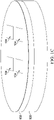
- FIGS. 1A-1H depict formation of an integrated silicon and III-N semiconductor device in successive stages of fabrication.
- FIG. 1A shows a silicon single-crystal first substrate 100 with a first crystal orientation, for example a ⁇ 111 ⁇ orientation.
- a layer stack of III-N semiconductor material 102 is formed on a top surface of the first substrate 100.
- the first crystal orientation may be selected to facilitate growth of the layer stack of III-N semiconductor material 102.
- the layer stack of III-N semiconductor material 102 may include, for example, a mismatch isolation layer of 100 to 300 nanometers of aluminum nitride formed on the top surface of the first substrate 100, and a buffer layer of 1 to 7 microns of graded layers of Al x Ga 1-x N, which is aluminum rich at the mismatch isolation layer and is gallium rich at a top surface of the buffer layer.
- the layer stack of III-N semiconductor material 102 may also include an electrical isolation layer of 300 to 2000 nanometers of semi-insulating gallium nitride formed on the buffer layer, and a low-defect layer of 25 to 1000 nanometers of gallium nitride formed on the electrical isolation layer.
- the layer stack of III-N semiconductor material 102 may also include a barrier layer formed on the low-defect layer.
- the barrier layer may be, for example, 8 to 30 nanometers of Al x Ga 1-x N or In x Al y Ga 1-x-y N.
- a composition of group III elements in the barrier layer may be, for example, 24 to 28 percent aluminum nitride and 72 to 76 percent gallium nitride.
- Forming the barrier layer on the low-defect layer generates a two-dimensional electron gas in the low-defect layer just below the barrier layer with an electron density of, for example, 1 ⁇ 10 12 to 2 ⁇ 10 13 cm -2 .
- the layer stack of III-N semiconductor material 102 may also include an optional cap layer of 2 to 5 nanometers of gallium nitride may be formed on the barrier layer.
- isolation regions 104 are formed in areas defined for a subsequent silicon film. Formation of the isolation regions 104 may include removal of material from the layer stack of III-N semiconductor material 102 so that the two-dimensional electron gas is disrupted in the isolation regions 104, as depicted in FIG. IB. Alternatively, formation of the isolation regions 104 may include ion implanting dopants so that the two-dimensional electron gas is disrupted in the isolation regions 104.
- dielectric material is formed in the isolation regions 104 and subsequently planarized to be substantially coplanar with a top surface of the layer stack of III-N semiconductor material 102, as depicted in FIG. 1C .
- the dielectric material may be, for example, silicon dioxide formed by a plasma enhanced chemical vapor deposition (PECVD) process using tetraethyl orthosilicate, also known as tetraethoxysilane or TEOS.
- PECVD plasma enhanced chemical vapor deposition
- a second silicon substrate 106 is provided with a second crystal orientation which is different than the first orientation of the first substrate 100.
- the second crystal orientation may be ⁇ 100 ⁇ .
- a cleaving species, such as hydrogen, is ion implanted into the second silicon substrate 106 at a sufficient dose and energy to form a separation layer 108 which is disposed between a silicon device film 110 and a carrier portion 112 of the second silicon substrate 106.
- the second crystal orientation may be selected to enhance performance of subsequently formed components in the silicon device film 110.
- the silicon device film 110 may be, for example, 2 to 5 microns thick.
- the cleaving species may be hydrogen, implanted at a dose of 5 ⁇ 10 16 cm -2 to 2 ⁇ 10 17 cm -2 at an energy of 225 keV for a 2 micron thickness of the silicon device film 110 to 450 keV for a 5 micron thickness.
- the silicon device film 110 may be cleaned in an aqueous mixture of hydrogen peroxide and ammonium hydroxide.
- a bonding operation is performed in which the silicon device film 110 is at least partially attached to the layer stack of III-N semiconductor material 102.
- the bonding operation may include, for example, pressing the silicon device film 110 and the layer stack of III-N semiconductor material 102 together at 0.8 megapascals to 1 megapascal pressure and 400 °C to 420 °C.
- the carrier portion 112 of the second silicon substrate 106 remains attached to the silicon device film 110 through the separation layer 108 during the bonding operation.
- a separation process is performed which separates the carrier portion 112 from the silicon device film 110 at the separation layer 108, leaving the silicon device film 110 bonded to the layer stack of III-N semiconductor material 102.
- the separation process includes heating the carrier portion 112 above 450 °C. Bonding between the silicon device film 110 and the layer stack of III-N semiconductor material 102 may become stronger during the separation process.
- the first substrate 100 remains attached to the layer stack of III-N semiconductor material 102.
- a portion of the silicon device film 110 is removed in areas for subsequent formation of components in the layer stack of III-N semiconductor material 102, leaving regions of the silicon device film 110 in place for subsequent formation of components in the silicon device film 110.
- the portion of the silicon device film 110 may be removed, for example, by forming an etch mask of photoresist which exposes the portion of the silicon device film 110 to be removed, and performing a silicon etch process to remove silicon in the exposed area. Other processes for removing the portion of the silicon device film 110 are within the scope of the instant embodiment.
- additional layers of III-N material may be formed on the layer stack of III-N semiconductor material 102 after the portion of the silicon device film 110 is removed.
- a first plurality of components 114 is formed in and/or on the silicon device film 110.
- the first plurality of components 114 may include, for example, MOS transistors as depicted in FIG. 1H .
- Other components such as bipolar junction transistors, diodes and resistors, are within the scope of the instant example.
- a second plurality of components 116 is formed in and/or on the layer stack of III-N semiconductor material 102.
- the second plurality of components 116 may include, for example, GaN FETs as depicted in FIG. 1H .
- Other components, such as photodetectors, LEDs or lasers are within the scope of the instant example.
- Integrated silicon and III-N semiconductor devices 118 include instances of both the first plurality of components 114 in the silicon device film 110 and instances of the second plurality of components 116 in the layer stack of III-N semiconductor material 102.
- the integrated silicon and III-N semiconductor devices 118 are outlined in FIG. 1H with the phantom lines.
- the integrated silicon and III-N semiconductor devices 118 may be separated by scribing, sawing, or other segmentation processes. Forming the integrated silicon and III-N semiconductor devices 118 using the process described in reference to FIG. 1A through FIG. 1H may advantageously provide a lower fabrication cost and complexity than other processes in which the layer stack of III-N semiconductor material 102 is transferred to a different substrate than one on which the layer stack of III-N semiconductor material 102 was originally formed.
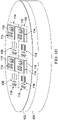
- FIGS. 2A-2F depict formation of another integrated silicon and III-N semiconductor device in successive stages of fabrication.
- a silicon single-crystal first substrate 200 is provided with a first crystal orientation, for example a ⁇ 111 ⁇ orientation.
- a layer stack of III-N semiconductor material 202 is formed on a top surface of the first substrate 200, as described in reference to FIG. 1A .
- Isolation regions 204 are formed in areas defined for a subsequent silicon film, as described for corresponding isolation regions 104 in reference to FIG. 1B and FIG. 1C .
- a first interlayer film 220 of dielectric material may be formed over the layer stack of III-N semiconductor material 202, and over the isolation regions 204.
- the first interlayer film 220 may be, for example, 10 to 100 nanometers of silicon dioxide based dielectric material formed by spinning on methylsilsesquioxane (MSQ) and subsequently baking out solvents and annealing the dielectric material.
- MSQ methylsilsesquioxane
- Other dielectric materials and other formation processes for the first interlayer film 220 are within the scope of the instant example.
- a second silicon substrate 206 is provided with a second crystal orientation, for example ⁇ 100 ⁇ , different than the first orientation of the first substrate 200.
- a separation layer 208 is formed between a silicon device film 210 and a carrier portion 212 of the second silicon substrate 206, as described in reference to FIG. ID.
- a second interlayer film 222 of dielectric material may be formed on the silicon device film 210.
- the second interlayer film 222 may be formed as described in reference to the first interlayer film 220.
- at least one of the first interlayer film 220 and the second interlayer film 222, and possibly both, is formed before proceeding to a subsequent bonding step.
- a bonding operation is performed in which the silicon device film 210 is at least partially bonded to the layer stack of III-N semiconductor material 202 through the first interlayer film 220 and/or the second interlayer film 222.
- the bonding operation may be similar to the bonding operation described in reference to FIG. IE.
- the carrier portion 212 of the second silicon substrate 206 remains attached to the silicon device film 210 through the separation layer 208 during the bonding operation.
- a separation process is performed which separates the carrier portion 212 from the silicon device film 210, leaving the silicon device film 210 bonded to the layer stack of III-N semiconductor material 202 through the first interlayer film 220 and/or the second interlayer film 222.
- the separation process includes heating the carrier portion 212 above 450 °C. Bonding between the silicon device film 210, the first interlayer film 220 and/or the second interlayer film 222, and the layer stack of III-N semiconductor material 202 may become stronger during the separation process.
- a portion of the silicon device film 210 and the underlying first interlayer film 220 and/or the second interlayer film 222 invention is removed in areas for subsequent formation of components in the layer stack of III-N semiconductor material 202, leaving regions of the silicon device film 210 and the underlying first interlayer film 220 and/or the second interlayer film 222 in place for subsequent formation of components in the silicon device film 210.
- the portion of the silicon device film 210 and the underlying first interlayer film 220 and/or the second interlayer film 222 may be removed, for example, as described in reference to FIG. 1G .
- additional layers of III-N material may be formed on the layer stack of III-N semiconductor material 202 after the portion of the silicon device film 210 and the underlying first interlayer film 220 and/or the second interlayer film 222 is removed.
- a first plurality of components 214 is formed in and/or on the silicon device film 210, and a second plurality of components 216 is formed in and/or on the layer stack of III-N semiconductor material 202, as described in reference to FIG. 1H .
- Integrated silicon and III-N semiconductor devices 218 include instances of both the first plurality of components 214 in the silicon device film 210 and instances of the second plurality of components 216 in the layer stack of III-N semiconductor material 202.
- the integrated silicon and III-N semiconductor devices 218 are outlined in FIG. 2F with the phantom lines.
- Forming the integrated silicon and III-N semiconductor devices 218 using the first interlayer film 220 and/or the second interlayer film 222 may provide a stronger structure including the silicon device film 210 and the layer stack of III-N semiconductor material 202 than a structure in which the silicon device film 210 is directly bonded to the layer stack of III-N semiconductor material 202.
- FIGS. 3A-3D are cross sections of a further integrated silicon and III-N semiconductor device in successive stages of fabrication. The process according to FIGS. 3A-3D is an example not forming part of the claimed invention.
- the integrated silicon and III-N semiconductor device 318 is formed on a silicon first substrate 300 with a layer stack of III-N semiconductor material 302 formed on the first substrate 300.
- a silicon device film 310 is bonded to the layer stack of III-N semiconductor material 302, possibly through an optional interlayer film 320 of dielectric material.
- the silicon device film 310 has a different crystal orientation from the first substrate 300.
- a first plurality of components 314 is at least partially formed in and/or on the silicon device film 310. Isolation regions may be formed in the layer stack of III-N semiconductor material 302 under the first plurality of components 314.
- an etch mask 324 is formed over the first plurality of components 314.
- the etch mask 324 may include, for example, photoresist formed by a photolithographic process.
- a silicon film etch process is performed which removes silicon from the silicon device film 310 in areas exposed by the etch mask 324.
- the interlayer film 320 if present, is also removed in the areas exposed by the etch mask 324.
- the etch mask 324 may be removed after the silicon film etch process is completed.
- an epitaxial blocking layer 326 is formed over the first plurality of components 314 and exposes an area of the layer stack of III-N semiconductor material 302 for subsequent epitaxial growth of III-N semiconductor material.
- the epitaxial blocking layer 326 may include, for example, 100 to 300 nanometers of silicon dioxide formed by PECVD using TEOS.
- additional III-N semiconductor material 328 is epitaxially grown on the exposed areas of the layer stack of III-N semiconductor material 302.
- the additional III-N semiconductor material 328 may include, for example, a barrier layer and gallium nitride cap. Formation of the barrier layer may generate a two-dimensional electron gas in an underlying gallium nitride layer. In such a case, formation of isolation regions in the under the layer stack of III-N semiconductor material 302 under the first plurality of components 314 may not be necessary, in contrast to the claimed invention.
- a second plurality of components 316 is formed in and/or on the additional III-N semiconductor material 328.
- the epitaxial blocking layer 326 is removed, possibly before the second plurality of components 316 is formed.
- Forming the additional III-N semiconductor material 328 after the silicon device film 310 is bonded to the layer stack of III-N semiconductor material 302 may advantageously provide higher performance in the second plurality of components 316, because the additional III-N semiconductor material 328 is not stressed by the bonding process.
Description
- This relates to methods of forming integrated silicon and III-N semiconductor devices.
- An integrated silicon and III-N semiconductor device may have electronic components such as metal oxide semiconductor (MOS) transistors formed in silicon, and other electronic components such as gallium nitride field effect transistors (GaN FETs) or optoelectronic components such as photodetectors, light emitting diodes (LEDs) or lasers formed in III-N semiconductor material, with the silicon and III-N semiconductor material disposed on a common substrate. It may be desirable to integrate the silicon and III-N semiconductor material on a common substrate prior to fabricating the components in the silicon and in the III-N semiconductor material.
- Such a method is known from H.-S. Lee et al.: "Wafer-Level Heterogeneous Integration of GaN HEMTs and Si (100) MOSFETs", IEEE Electron Device Letters, Vol. 33, No. 2, February 2012, pages 200-202. The key step of this method is the fabrication of a Si (100)-GaN-Si hybrid wafer by bonding a silicon (100) on insulator (SOI) wafer to the nitride surface of an AlGaN/GaN on Si (111) wafer. A thin layer of silicon oxide is used to enhance the bonding between the SOI and the AlGaN/GaN wafers. Once the hybrid wafer has been fabricated, a standard Si process technology can be used for the fabrication of the Si devices. For the fabrication of GaN devices, the Si (100) active layer is selectively removed from the regions where GaN transistors are needed. The devices are then isolated by mesa etching with a BCl3/Cl2-based plasma.
- Further methods of forming integrated III-V and silicon devices are known from
US Patent Application Publications 2006/0284247 A1 and2012/0280326 A1 . - According to the invention, a method according to claim 1 is provided. Preferred embodiments are defined in claims 2-11.
- Some steps of the method are explained in the following:
An integrated silicon and III-N semiconductor device is formed by growing III-N semiconductor material on a first silicon substrate having a first orientation. Planar isolation regions are formed in areas for a silicon device film to be formed. - A second silicon substrate with a second, different, orientation is ion implanted with a separating species to form a release layer between a silicon device film at a top surface of the second silicon substrate and a carrier wafer at a bottom of the second silicon substrate. The silicon device film is attached to the III-N semiconductor material while the silicon device film is connected to the carrier wafer through the release layer. The carrier wafer is subsequently removed from the silicon device film. The silicon device film is then bonded to the III-N semiconductor material. A first plurality of components is formed in and/or on the silicon device film. A portion of the silicon device film is removed to expose the III-N semiconductor material. A second plurality of components is formed in and/or on III-N semiconductor material in the exposed region.
- Optionally, a dielectric interlayer may be formed on the silicon device film and/or the III-N semiconductor material prior to the attaching step, so that the dielectric interlayer is disposed between the silicon device film and the III-N semiconductor material in the integrated silicon and III-N semiconductor device.
-
-
FIGS. 1A-1H depict formation of an integrated silicon and III-N semiconductor device in successive stages of fabrication. -
FIGS. 2A-2F depict formation of another integrated silicon and III-N semiconductor device in successive stages of fabrication. -
FIGS. 3A-3D are cross sections of a further integrated silicon and III-N semiconductor device in successive stages of fabrication. The manufacturing method according toFIGS. 3A-3D is an example not forming part of the claimed invention. - III-N semiconductor materials are materials in which Group III (boron group) elements (boron, aluminum, gallium, indium) provide a portion of the atoms in the semiconductor material and nitrogen atoms provide the remainder. Examples of III-N semiconductor materials are gallium nitride, boron gallium nitride, aluminum gallium nitride, indium nitride, and indium aluminum gallium nitride. III-N materials may be written with variable subscripts to denote a range of possible stoichiometries. For example, aluminum gallium nitride may be written as AlxGa1-xN and indium aluminum gallium nitride may be written as InxAlyGa1-x-yN. GaN FET is an example of a field effect transistor that includes III-N semiconductor materials.
-
FIGS. 1A-1H depict formation of an integrated silicon and III-N semiconductor device in successive stages of fabrication. -
FIG. 1A shows a silicon single-crystalfirst substrate 100 with a first crystal orientation, for example a {111} orientation. A layer stack of III-N semiconductor material 102 is formed on a top surface of thefirst substrate 100. The first crystal orientation may be selected to facilitate growth of the layer stack of III-N semiconductor material 102. The layer stack of III-N semiconductor material 102 may include, for example, a mismatch isolation layer of 100 to 300 nanometers of aluminum nitride formed on the top surface of thefirst substrate 100, and a buffer layer of 1 to 7 microns of graded layers of AlxGa1-xN, which is aluminum rich at the mismatch isolation layer and is gallium rich at a top surface of the buffer layer. In some versions of the instant embodiment, the layer stack of III-N semiconductor material 102 may also include an electrical isolation layer of 300 to 2000 nanometers of semi-insulating gallium nitride formed on the buffer layer, and a low-defect layer of 25 to 1000 nanometers of gallium nitride formed on the electrical isolation layer. - In further versions of the instant embodiment, the layer stack of III-
N semiconductor material 102 may also include a barrier layer formed on the low-defect layer. The barrier layer may be, for example, 8 to 30 nanometers of AlxGa1-xN or InxAlyGa1-x-yN. A composition of group III elements in the barrier layer may be, for example, 24 to 28 percent aluminum nitride and 72 to 76 percent gallium nitride. Forming the barrier layer on the low-defect layer generates a two-dimensional electron gas in the low-defect layer just below the barrier layer with an electron density of, for example, 1×10¹² to 2×1013 cm-2. The layer stack of III-N semiconductor material 102 may also include an optional cap layer of 2 to 5 nanometers of gallium nitride may be formed on the barrier layer. - In
FIG. 1B , according to the invention,isolation regions 104 are formed in areas defined for a subsequent silicon film. Formation of theisolation regions 104 may include removal of material from the layer stack of III-N semiconductor material 102 so that the two-dimensional electron gas is disrupted in theisolation regions 104, as depicted in FIG. IB. Alternatively, formation of theisolation regions 104 may include ion implanting dopants so that the two-dimensional electron gas is disrupted in theisolation regions 104. - In
FIG. 1C , in versions of the instant embodiment in which material is removed from the layer stack of III-N semiconductor material 102 in theisolation regions 104, dielectric material is formed in theisolation regions 104 and subsequently planarized to be substantially coplanar with a top surface of the layer stack of III-N semiconductor material 102, as depicted inFIG. 1C . The dielectric material may be, for example, silicon dioxide formed by a plasma enhanced chemical vapor deposition (PECVD) process using tetraethyl orthosilicate, also known as tetraethoxysilane or TEOS. - In
FIG. 1D , asecond silicon substrate 106 is provided with a second crystal orientation which is different than the first orientation of thefirst substrate 100. For example, the second crystal orientation may be {100}. A cleaving species, such as hydrogen, is ion implanted into thesecond silicon substrate 106 at a sufficient dose and energy to form aseparation layer 108 which is disposed between asilicon device film 110 and acarrier portion 112 of thesecond silicon substrate 106. The second crystal orientation may be selected to enhance performance of subsequently formed components in thesilicon device film 110. Thesilicon device film 110 may be, for example, 2 to 5 microns thick. The cleaving species may be hydrogen, implanted at a dose of 5×1016 cm-2 to 2×1017 cm-2 at an energy of 225 keV for a 2 micron thickness of thesilicon device film 110 to 450 keV for a 5 micron thickness. After theseparation layer 108 is formed, thesilicon device film 110 may be cleaned in an aqueous mixture of hydrogen peroxide and ammonium hydroxide. - In FIG. IE, a bonding operation is performed in which the
silicon device film 110 is at least partially attached to the layer stack of III-N semiconductor material 102. The bonding operation may include, for example, pressing thesilicon device film 110 and the layer stack of III-N semiconductor material 102 together at 0.8 megapascals to 1 megapascal pressure and 400 °C to 420 °C. Thecarrier portion 112 of thesecond silicon substrate 106 remains attached to thesilicon device film 110 through theseparation layer 108 during the bonding operation. - In FIG. IF, a separation process is performed which separates the
carrier portion 112 from thesilicon device film 110 at theseparation layer 108, leaving thesilicon device film 110 bonded to the layer stack of III-N semiconductor material 102. The separation process includes heating thecarrier portion 112 above 450 °C. Bonding between thesilicon device film 110 and the layer stack of III-N semiconductor material 102 may become stronger during the separation process. Thefirst substrate 100 remains attached to the layer stack of III-N semiconductor material 102. - In
FIG. 1G , a portion of thesilicon device film 110 is removed in areas for subsequent formation of components in the layer stack of III-N semiconductor material 102, leaving regions of thesilicon device film 110 in place for subsequent formation of components in thesilicon device film 110. The portion of thesilicon device film 110 may be removed, for example, by forming an etch mask of photoresist which exposes the portion of thesilicon device film 110 to be removed, and performing a silicon etch process to remove silicon in the exposed area. Other processes for removing the portion of thesilicon device film 110 are within the scope of the instant embodiment. In some versions of the instant embodiment, additional layers of III-N material may be formed on the layer stack of III-N semiconductor material 102 after the portion of thesilicon device film 110 is removed. - In
FIG. 1H , a first plurality ofcomponents 114 is formed in and/or on thesilicon device film 110. The first plurality ofcomponents 114 may include, for example, MOS transistors as depicted inFIG. 1H . Other components, such as bipolar junction transistors, diodes and resistors, are within the scope of the instant example. A second plurality ofcomponents 116 is formed in and/or on the layer stack of III-N semiconductor material 102. The second plurality ofcomponents 116 may include, for example, GaN FETs as depicted inFIG. 1H . Other components, such as photodetectors, LEDs or lasers are within the scope of the instant example. Integrated silicon and III-N semiconductor devices 118 include instances of both the first plurality ofcomponents 114 in thesilicon device film 110 and instances of the second plurality ofcomponents 116 in the layer stack of III-N semiconductor material 102. The integrated silicon and III-N semiconductor devices 118 are outlined inFIG. 1H with the phantom lines. The integrated silicon and III-N semiconductor devices 118 may be separated by scribing, sawing, or other segmentation processes. Forming the integrated silicon and III-N semiconductor devices 118 using the process described in reference toFIG. 1A through FIG. 1H may advantageously provide a lower fabrication cost and complexity than other processes in which the layer stack of III-N semiconductor material 102 is transferred to a different substrate than one on which the layer stack of III-N semiconductor material 102 was originally formed. -
FIGS. 2A-2F depict formation of another integrated silicon and III-N semiconductor device in successive stages of fabrication. InFIG. 2A , a silicon single-crystalfirst substrate 200 is provided with a first crystal orientation, for example a {111} orientation. A layer stack of III-N semiconductor material 202 is formed on a top surface of thefirst substrate 200, as described in reference toFIG. 1A .Isolation regions 204 are formed in areas defined for a subsequent silicon film, as described forcorresponding isolation regions 104 in reference toFIG. 1B andFIG. 1C . Afirst interlayer film 220 of dielectric material may be formed over the layer stack of III-N semiconductor material 202, and over theisolation regions 204. Thefirst interlayer film 220 may be, for example, 10 to 100 nanometers of silicon dioxide based dielectric material formed by spinning on methylsilsesquioxane (MSQ) and subsequently baking out solvents and annealing the dielectric material. Other dielectric materials and other formation processes for thefirst interlayer film 220 are within the scope of the instant example. - In
FIG. 2B , asecond silicon substrate 206 is provided with a second crystal orientation, for example {100}, different than the first orientation of thefirst substrate 200. Aseparation layer 208 is formed between asilicon device film 210 and acarrier portion 212 of thesecond silicon substrate 206, as described in reference to FIG. ID. Asecond interlayer film 222 of dielectric material may be formed on thesilicon device film 210. Thesecond interlayer film 222 may be formed as described in reference to thefirst interlayer film 220. In the instant embodiment, at least one of thefirst interlayer film 220 and thesecond interlayer film 222, and possibly both, is formed before proceeding to a subsequent bonding step. - In
FIG. 2C , a bonding operation is performed in which thesilicon device film 210 is at least partially bonded to the layer stack of III-N semiconductor material 202 through thefirst interlayer film 220 and/or thesecond interlayer film 222. The bonding operation may be similar to the bonding operation described in reference to FIG. IE. Thecarrier portion 212 of thesecond silicon substrate 206 remains attached to thesilicon device film 210 through theseparation layer 208 during the bonding operation. - In
FIG. 2D , a separation process is performed which separates thecarrier portion 212 from thesilicon device film 210, leaving thesilicon device film 210 bonded to the layer stack of III-N semiconductor material 202 through thefirst interlayer film 220 and/or thesecond interlayer film 222. The separation process includes heating thecarrier portion 212 above 450 °C. Bonding between thesilicon device film 210, thefirst interlayer film 220 and/or thesecond interlayer film 222, and the layer stack of III-N semiconductor material 202 may become stronger during the separation process. - In
FIG. 2E , a portion of thesilicon device film 210 and the underlyingfirst interlayer film 220 and/or thesecond interlayer film 222 invention is removed in areas for subsequent formation of components in the layer stack of III-N semiconductor material 202, leaving regions of thesilicon device film 210 and the underlyingfirst interlayer film 220 and/or thesecond interlayer film 222 in place for subsequent formation of components in thesilicon device film 210. The portion of thesilicon device film 210 and the underlyingfirst interlayer film 220 and/or thesecond interlayer film 222 may be removed, for example, as described in reference toFIG. 1G . In some versions of the instant embodiment, additional layers of III-N material may be formed on the layer stack of III-N semiconductor material 202 after the portion of thesilicon device film 210 and the underlyingfirst interlayer film 220 and/or thesecond interlayer film 222 is removed. - In
FIG. 2F , a first plurality ofcomponents 214 is formed in and/or on thesilicon device film 210, and a second plurality ofcomponents 216 is formed in and/or on the layer stack of III-N semiconductor material 202, as described in reference toFIG. 1H . Integrated silicon and III-N semiconductor devices 218 include instances of both the first plurality ofcomponents 214 in thesilicon device film 210 and instances of the second plurality ofcomponents 216 in the layer stack of III-N semiconductor material 202. The integrated silicon and III-N semiconductor devices 218 are outlined inFIG. 2F with the phantom lines. Forming the integrated silicon and III-N semiconductor devices 218 using thefirst interlayer film 220 and/or thesecond interlayer film 222 may provide a stronger structure including thesilicon device film 210 and the layer stack of III-N semiconductor material 202 than a structure in which thesilicon device film 210 is directly bonded to the layer stack of III-N semiconductor material 202. -
FIGS. 3A-3D are cross sections of a further integrated silicon and III-N semiconductor device in successive stages of fabrication. The process according toFIGS. 3A-3D is an example not forming part of the claimed invention. - In
FIG. 3A , the integrated silicon and III-N semiconductor device 318 is formed on a siliconfirst substrate 300 with a layer stack of III-N semiconductor material 302 formed on thefirst substrate 300. Asilicon device film 310 is bonded to the layer stack of III-N semiconductor material 302, possibly through anoptional interlayer film 320 of dielectric material. Thesilicon device film 310 has a different crystal orientation from thefirst substrate 300. A first plurality ofcomponents 314 is at least partially formed in and/or on thesilicon device film 310. Isolation regions may be formed in the layer stack of III-N semiconductor material 302 under the first plurality ofcomponents 314. - In
FIG. 3B , anetch mask 324 is formed over the first plurality ofcomponents 314. Theetch mask 324 may include, for example, photoresist formed by a photolithographic process. A silicon film etch process is performed which removes silicon from thesilicon device film 310 in areas exposed by theetch mask 324. Theinterlayer film 320, if present, is also removed in the areas exposed by theetch mask 324. Theetch mask 324 may be removed after the silicon film etch process is completed. - In
FIG. 3C , anepitaxial blocking layer 326 is formed over the first plurality ofcomponents 314 and exposes an area of the layer stack of III-N semiconductor material 302 for subsequent epitaxial growth of III-N semiconductor material. Theepitaxial blocking layer 326 may include, for example, 100 to 300 nanometers of silicon dioxide formed by PECVD using TEOS. - Subsequently, additional III-
N semiconductor material 328 is epitaxially grown on the exposed areas of the layer stack of III-N semiconductor material 302. The additional III-N semiconductor material 328 may include, for example, a barrier layer and gallium nitride cap. Formation of the barrier layer may generate a two-dimensional electron gas in an underlying gallium nitride layer. In such a case, formation of isolation regions in the under the layer stack of III-N semiconductor material 302 under the first plurality ofcomponents 314 may not be necessary, in contrast to the claimed invention. - In
FIG. 3D , a second plurality ofcomponents 316 is formed in and/or on the additional III-N semiconductor material 328. Theepitaxial blocking layer 326 is removed, possibly before the second plurality ofcomponents 316 is formed. Forming the additional III-N semiconductor material 328 after thesilicon device film 310 is bonded to the layer stack of III-N semiconductor material 302 may advantageously provide higher performance in the second plurality ofcomponents 316, because the additional III-N semiconductor material 328 is not stressed by the bonding process. - Those skilled in the art will appreciate that modifications may be made to the described embodiments according to
FIGS. 1 and2 , and also that many other embodiments are possible, within the scope of the present invention as defined in the appended claims.
Claims (11)
- A method of forming an integrated silicon and III-N semiconductor device, comprising:providing a first substrate (100, 200) of silicon having a first crystal orientation;forming a layer stack of III-N semiconductor material (102, 202) on a top surface of the first substrate (100, 200);defining areas on the first substrate for a silicon device film (110, 210) to be formed;forming isolation regions (104, 204) on the first substrate (100, 200) in the layer stack of III-N material (102, 202) in said areas defined for the silicon device film (110, 210) to be formed;if forming isolation regions (104, 204) comprises removing material, forming dielectric material in the isolation regions and planarising the dielectric material to be coplanar with a top surface of the III-N semiconductor material (102, 202);providing a second substrate of silicon (106, 206) having a second crystal orientation which is different from the first crystal orientation;implanting a cleaving species into said second substrate to form a separation layer (108, 208) in the second substrate which separates the silicon device film (110, 210) from a carrier portion (112, 212) of the second substrate;bonding the silicon device film to the layer stack of III-N semiconductor material, so that the carrier portion remains attached to the silicon device film through the separation layer;after bonding, heating the carrier portion (112, 212) to a temperature above 450 °C to separate the carrier portion from the silicon device film at the separation layer, so that the first substrate remains attached to the layer stack of III-N semiconductor material;removing a portion of the silicon device film (110, 210) so as to expose an area of the layer stack of III-N semiconductor material (102, 202), leaving regions of the silicon device film (110, 210) in place in said areas defined for the silicon device film;forming a first plurality of components (114, 214) in and/or on the silicon device film over the isolation regions (104, 204) in the layer stack of III-N semiconductor material (102, 202); andforming a second plurality of components (116, 216) in and/or on the layer stack of III-N semiconductor material.
- The method of claim 1, further comprising the step of forming an interlayer film (220, 222) of dielectric material on at least one of (i) the silicon device film (210) and (ii) the layer stack of III-N semiconductor material (202) with the isolation regions (204) formed therein, prior to the step of bonding.
- The method of claim 2, wherein the interlayer film (222) is formed on the silicon device film (210) prior to the step of bonding.
- The method of claim 2, wherein the interlayer film (220) is formed on the layer stack of III-N semiconductor material (202) prior to the step of bonding.
- The method of claim 2, wherein the interlayer film (220, 222) includes silicon dioxide based dielectric material.
- The method of claim 1, wherein the step of forming the isolation regions (104, 204) includes ion implanting dopants into the layer stack of III-N semiconductor material (102, 202) in the isolation regions (104, 204).
- The method of claim 1, wherein the step of forming the isolation regions (104, 204) includes removing III-N semiconductor material from the layer stack of III-N semiconductor material (102, 202) in the isolation regions.
- The method of claim 1, wherein the first crystal orientation is {111}.
- The method of claim 1, wherein the second crystal orientation is {100}.
- The method of claim 1, wherein the first plurality of components includes a metal oxide semiconductor transistor.
- The method of claim 1, wherein the second plurality of components includes a gallium nitride field effect transistor.
Applications Claiming Priority (2)
| Application Number | Priority Date | Filing Date | Title |
|---|---|---|---|
| US13/886,652 US9396948B2 (en) | 2013-05-03 | 2013-05-03 | Layer transfer of silicon onto III-nitride material for heterogenous integration |
| PCT/US2014/036794 WO2014179797A1 (en) | 2013-05-03 | 2014-05-05 | Integrated silicon and iii-n semiconductor device |
Publications (3)
| Publication Number | Publication Date |
|---|---|
| EP3008751A1 EP3008751A1 (en) | 2016-04-20 |
| EP3008751A4 EP3008751A4 (en) | 2017-03-15 |
| EP3008751B1 true EP3008751B1 (en) | 2022-07-06 |
Family
ID=51841622
Family Applications (1)
| Application Number | Title | Priority Date | Filing Date |
|---|---|---|---|
| EP14791900.5A Active EP3008751B1 (en) | 2013-05-03 | 2014-05-05 | Method of forming an integrated silicon and iii-n semiconductor device |
Country Status (4)
| Country | Link |
|---|---|
| US (1) | US9396948B2 (en) |
| EP (1) | EP3008751B1 (en) |
| CN (1) | CN105164800B (en) |
| WO (1) | WO2014179797A1 (en) |
Families Citing this family (2)
| Publication number | Priority date | Publication date | Assignee | Title |
|---|---|---|---|---|
| US10453679B2 (en) | 2015-08-28 | 2019-10-22 | Intel Corporation | Methods and devices integrating III-N transistor circuitry with Si transistor circuitry |
| EP3761343A1 (en) * | 2019-07-03 | 2021-01-06 | IMEC vzw | Method for manufacturing a silicon on nitride substrate |
Family Cites Families (14)
| Publication number | Priority date | Publication date | Assignee | Title |
|---|---|---|---|---|
| JPH04299518A (en) * | 1991-03-27 | 1992-10-22 | Nippondenso Co Ltd | Semiconductor device and manufacture thereof |
| US7119365B2 (en) * | 2002-03-26 | 2006-10-10 | Sharp Kabushiki Kaisha | Semiconductor device and manufacturing method thereof, SOI substrate and display device using the same, and manufacturing method of the SOI substrate |
| US20070090491A1 (en) * | 2003-04-07 | 2007-04-26 | United Microelectronics Corp. | Semiconductor structure with silicon on insulator |
| US7348658B2 (en) * | 2004-08-30 | 2008-03-25 | International Business Machines Corporation | Multilayer silicon over insulator device |
| US7420226B2 (en) * | 2005-06-17 | 2008-09-02 | Northrop Grumman Corporation | Method for integrating silicon CMOS and AlGaN/GaN wideband amplifiers on engineered substrates |
| US7217629B2 (en) * | 2005-07-15 | 2007-05-15 | International Business Machines Corporation | Epitaxial imprinting |
| WO2007053686A2 (en) * | 2005-11-01 | 2007-05-10 | Massachusetts Institute Of Technology | Monolithically integrated semiconductor materials and devices |
| US7897994B2 (en) * | 2007-06-18 | 2011-03-01 | Texas Instruments Incorporated | Method of making (100) NMOS and (110) PMOS sidewall surface on the same fin orientation for multiple gate MOSFET with DSB substrate |
| KR101572476B1 (en) * | 2008-12-12 | 2015-11-27 | 주식회사 동부하이텍 | semiconductor and method of manufacturing the same |
| US7994550B2 (en) * | 2009-05-22 | 2011-08-09 | Raytheon Company | Semiconductor structures having both elemental and compound semiconductor devices on a common substrate |
| US8212294B2 (en) * | 2010-01-28 | 2012-07-03 | Raytheon Company | Structure having silicon CMOS transistors with column III-V transistors on a common substrate |
| US8912055B2 (en) * | 2011-05-03 | 2014-12-16 | Imec | Method for manufacturing a hybrid MOSFET device and hybrid MOSFET obtainable thereby |
| CN102790004B (en) * | 2011-05-16 | 2014-06-11 | 中国科学院上海微系统与信息技术研究所 | Preparation method of full-isolation mixed crystal orientation crystal orientation silicon-on-insulator (SOI) |
| US8916909B2 (en) * | 2012-03-06 | 2014-12-23 | Infineon Technologies Austria Ag | Semiconductor device and method for fabricating a semiconductor device |
-
2013
- 2013-05-03 US US13/886,652 patent/US9396948B2/en active Active
-
2014
- 2014-05-05 WO PCT/US2014/036794 patent/WO2014179797A1/en active Application Filing
- 2014-05-05 CN CN201480024816.6A patent/CN105164800B/en active Active
- 2014-05-05 EP EP14791900.5A patent/EP3008751B1/en active Active
Also Published As
| Publication number | Publication date |
|---|---|
| CN105164800A (en) | 2015-12-16 |
| US9396948B2 (en) | 2016-07-19 |
| CN105164800B (en) | 2019-01-18 |
| EP3008751A1 (en) | 2016-04-20 |
| WO2014179797A1 (en) | 2014-11-06 |
| US20140329370A1 (en) | 2014-11-06 |
| EP3008751A4 (en) | 2017-03-15 |
Similar Documents
| Publication | Publication Date | Title |
|---|---|---|
| US10074588B2 (en) | Semiconductor devices with a thermally conductive layer and methods of their fabrication | |
| CN109844184B (en) | Engineered substrate structures for power and radio frequency applications | |
| EP2317554B1 (en) | Integrated semiconductor substrate structure and method of manufacturing an integrated semiconductor substrate structure | |
| TWI355017B (en) | Method for producing semiconductor device | |
| JP2022106775A (en) | Electronic power devices integrated with engineered substrate | |
| US8759169B2 (en) | Method for producing silicon semiconductor wafers comprising a layer for integrating III-V semiconductor components | |
| US20040012037A1 (en) | Hetero-integration of semiconductor materials on silicon | |
| CN111512415B (en) | System and method for engineering integrated devices on a substrate | |
| US20130062696A1 (en) | SOI Semiconductor Structure with a Hybrid of Coplanar Germanium and III-V, and Preparation Method thereof | |
| CN111566827A (en) | Power and RF devices implemented with engineered substrate structures | |
| US20160343810A1 (en) | Method for manufacturing semiconductor device using high speed epitaxial lift-off and template for iii-v direct growth and semiconductor device manufactured using the same | |
| CN110291645B (en) | Method and system for vertical power device | |
| US11011410B2 (en) | Substrate having two semiconductor materials on insulator | |
| JP7332634B2 (en) | Reduction of parasitic capacitance in GaN-on-silicon devices | |
| KR102196071B1 (en) | Process to form soi substrate | |
| US8546207B2 (en) | Method for fabricating semiconductor wafers for the integration of silicon components with HEMTs, and appropriate semiconductor layer arrangement | |
| EP3008751B1 (en) | Method of forming an integrated silicon and iii-n semiconductor device | |
| US20210013335A1 (en) | Insulating structure of high electron mobility transistor and manufacturing method thereof | |
| US9406564B2 (en) | Singulation through a masking structure surrounding expitaxial regions | |
| US20230395376A1 (en) | Semiconductor substrates and methods of producing the same | |
| EP4287247A1 (en) | A method for producing a semiconductor chip | |
| US9209065B1 (en) | Engineered substrate and device for co-integration of strained silicon and relaxed silicon | |
| JP2019176110A (en) | Method for manufacturing semiconductor device | |
| US20140264456A1 (en) | Method of forming a high electron mobility semiconductor device |
Legal Events
| Date | Code | Title | Description |
|---|---|---|---|
| PUAI | Public reference made under article 153(3) epc to a published international application that has entered the european phase |
Free format text: ORIGINAL CODE: 0009012 |
|
| 17P | Request for examination filed |
Effective date: 20151222 |
|
| AK | Designated contracting states |
Kind code of ref document: A1 Designated state(s): AL AT BE BG CH CY CZ DE DK EE ES FI FR GB GR HR HU IE IS IT LI LT LU LV MC MK MT NL NO PL PT RO RS SE SI SK SM TR |
|
| AX | Request for extension of the european patent |
Extension state: BA ME |
|
| DAX | Request for extension of the european patent (deleted) | ||
| REG | Reference to a national code |
Ref country code: DE Ref legal event code: R079 Ref document number: 602014084237 Country of ref document: DE Free format text: PREVIOUS MAIN CLASS: H01L0021700000 Ipc: H01L0021825800 |
|
| A4 | Supplementary search report drawn up and despatched |
Effective date: 20170209 |
|
| RIC1 | Information provided on ipc code assigned before grant |
Ipc: H01L 21/18 20060101ALI20170203BHEP Ipc: H01L 21/8258 20060101AFI20170203BHEP |
|
| STAA | Information on the status of an ep patent application or granted ep patent |
Free format text: STATUS: REQUEST FOR EXAMINATION WAS MADE |
|
| STAA | Information on the status of an ep patent application or granted ep patent |
Free format text: STATUS: EXAMINATION IS IN PROGRESS |
|
| 17Q | First examination report despatched |
Effective date: 20200403 |
|
| STAA | Information on the status of an ep patent application or granted ep patent |
Free format text: STATUS: EXAMINATION IS IN PROGRESS |
|
| GRAP | Despatch of communication of intention to grant a patent |
Free format text: ORIGINAL CODE: EPIDOSNIGR1 |
|
| STAA | Information on the status of an ep patent application or granted ep patent |
Free format text: STATUS: GRANT OF PATENT IS INTENDED |
|
| INTG | Intention to grant announced |
Effective date: 20211209 |
|
| GRAS | Grant fee paid |
Free format text: ORIGINAL CODE: EPIDOSNIGR3 |
|
| GRAA | (expected) grant |
Free format text: ORIGINAL CODE: 0009210 |
|
| STAA | Information on the status of an ep patent application or granted ep patent |
Free format text: STATUS: THE PATENT HAS BEEN GRANTED |
|
| AK | Designated contracting states |
Kind code of ref document: B1 Designated state(s): AL AT BE BG CH CY CZ DE DK EE ES FI FR GB GR HR HU IE IS IT LI LT LU LV MC MK MT NL NO PL PT RO RS SE SI SK SM TR |
|
| REG | Reference to a national code |
Ref country code: GB Ref legal event code: FG4D |
|
| REG | Reference to a national code |
Ref country code: AT Ref legal event code: REF Ref document number: 1503476 Country of ref document: AT Kind code of ref document: T Effective date: 20220715 Ref country code: CH Ref legal event code: EP |
|
| REG | Reference to a national code |
Ref country code: DE Ref legal event code: R096 Ref document number: 602014084237 Country of ref document: DE |
|
| REG | Reference to a national code |
Ref country code: IE Ref legal event code: FG4D |
|
| REG | Reference to a national code |
Ref country code: LT Ref legal event code: MG9D |
|
| REG | Reference to a national code |
Ref country code: NL Ref legal event code: MP Effective date: 20220706 |
|
| PG25 | Lapsed in a contracting state [announced via postgrant information from national office to epo] |
Ref country code: SE Free format text: LAPSE BECAUSE OF FAILURE TO SUBMIT A TRANSLATION OF THE DESCRIPTION OR TO PAY THE FEE WITHIN THE PRESCRIBED TIME-LIMIT Effective date: 20220706 Ref country code: RS Free format text: LAPSE BECAUSE OF FAILURE TO SUBMIT A TRANSLATION OF THE DESCRIPTION OR TO PAY THE FEE WITHIN THE PRESCRIBED TIME-LIMIT Effective date: 20220706 Ref country code: PT Free format text: LAPSE BECAUSE OF FAILURE TO SUBMIT A TRANSLATION OF THE DESCRIPTION OR TO PAY THE FEE WITHIN THE PRESCRIBED TIME-LIMIT Effective date: 20221107 Ref country code: NO Free format text: LAPSE BECAUSE OF FAILURE TO SUBMIT A TRANSLATION OF THE DESCRIPTION OR TO PAY THE FEE WITHIN THE PRESCRIBED TIME-LIMIT Effective date: 20221006 Ref country code: NL Free format text: LAPSE BECAUSE OF FAILURE TO SUBMIT A TRANSLATION OF THE DESCRIPTION OR TO PAY THE FEE WITHIN THE PRESCRIBED TIME-LIMIT Effective date: 20220706 Ref country code: LV Free format text: LAPSE BECAUSE OF FAILURE TO SUBMIT A TRANSLATION OF THE DESCRIPTION OR TO PAY THE FEE WITHIN THE PRESCRIBED TIME-LIMIT Effective date: 20220706 Ref country code: LT Free format text: LAPSE BECAUSE OF FAILURE TO SUBMIT A TRANSLATION OF THE DESCRIPTION OR TO PAY THE FEE WITHIN THE PRESCRIBED TIME-LIMIT Effective date: 20220706 Ref country code: FI Free format text: LAPSE BECAUSE OF FAILURE TO SUBMIT A TRANSLATION OF THE DESCRIPTION OR TO PAY THE FEE WITHIN THE PRESCRIBED TIME-LIMIT Effective date: 20220706 Ref country code: ES Free format text: LAPSE BECAUSE OF FAILURE TO SUBMIT A TRANSLATION OF THE DESCRIPTION OR TO PAY THE FEE WITHIN THE PRESCRIBED TIME-LIMIT Effective date: 20220706 |
|
| REG | Reference to a national code |
Ref country code: AT Ref legal event code: MK05 Ref document number: 1503476 Country of ref document: AT Kind code of ref document: T Effective date: 20220706 |
|
| PG25 | Lapsed in a contracting state [announced via postgrant information from national office to epo] |
Ref country code: PL Free format text: LAPSE BECAUSE OF FAILURE TO SUBMIT A TRANSLATION OF THE DESCRIPTION OR TO PAY THE FEE WITHIN THE PRESCRIBED TIME-LIMIT Effective date: 20220706 Ref country code: IS Free format text: LAPSE BECAUSE OF FAILURE TO SUBMIT A TRANSLATION OF THE DESCRIPTION OR TO PAY THE FEE WITHIN THE PRESCRIBED TIME-LIMIT Effective date: 20221106 Ref country code: HR Free format text: LAPSE BECAUSE OF FAILURE TO SUBMIT A TRANSLATION OF THE DESCRIPTION OR TO PAY THE FEE WITHIN THE PRESCRIBED TIME-LIMIT Effective date: 20220706 Ref country code: GR Free format text: LAPSE BECAUSE OF FAILURE TO SUBMIT A TRANSLATION OF THE DESCRIPTION OR TO PAY THE FEE WITHIN THE PRESCRIBED TIME-LIMIT Effective date: 20221007 |
|
| REG | Reference to a national code |
Ref country code: DE Ref legal event code: R097 Ref document number: 602014084237 Country of ref document: DE |
|
| PG25 | Lapsed in a contracting state [announced via postgrant information from national office to epo] |
Ref country code: SM Free format text: LAPSE BECAUSE OF FAILURE TO SUBMIT A TRANSLATION OF THE DESCRIPTION OR TO PAY THE FEE WITHIN THE PRESCRIBED TIME-LIMIT Effective date: 20220706 Ref country code: RO Free format text: LAPSE BECAUSE OF FAILURE TO SUBMIT A TRANSLATION OF THE DESCRIPTION OR TO PAY THE FEE WITHIN THE PRESCRIBED TIME-LIMIT Effective date: 20220706 Ref country code: DK Free format text: LAPSE BECAUSE OF FAILURE TO SUBMIT A TRANSLATION OF THE DESCRIPTION OR TO PAY THE FEE WITHIN THE PRESCRIBED TIME-LIMIT Effective date: 20220706 Ref country code: CZ Free format text: LAPSE BECAUSE OF FAILURE TO SUBMIT A TRANSLATION OF THE DESCRIPTION OR TO PAY THE FEE WITHIN THE PRESCRIBED TIME-LIMIT Effective date: 20220706 Ref country code: AT Free format text: LAPSE BECAUSE OF FAILURE TO SUBMIT A TRANSLATION OF THE DESCRIPTION OR TO PAY THE FEE WITHIN THE PRESCRIBED TIME-LIMIT Effective date: 20220706 |
|
| PLBE | No opposition filed within time limit |
Free format text: ORIGINAL CODE: 0009261 |
|
| STAA | Information on the status of an ep patent application or granted ep patent |
Free format text: STATUS: NO OPPOSITION FILED WITHIN TIME LIMIT |
|
| PG25 | Lapsed in a contracting state [announced via postgrant information from national office to epo] |
Ref country code: SK Free format text: LAPSE BECAUSE OF FAILURE TO SUBMIT A TRANSLATION OF THE DESCRIPTION OR TO PAY THE FEE WITHIN THE PRESCRIBED TIME-LIMIT Effective date: 20220706 Ref country code: EE Free format text: LAPSE BECAUSE OF FAILURE TO SUBMIT A TRANSLATION OF THE DESCRIPTION OR TO PAY THE FEE WITHIN THE PRESCRIBED TIME-LIMIT Effective date: 20220706 |
|
| 26N | No opposition filed |
Effective date: 20230411 |
|
| P01 | Opt-out of the competence of the unified patent court (upc) registered |
Effective date: 20230523 |
|
| PG25 | Lapsed in a contracting state [announced via postgrant information from national office to epo] |
Ref country code: AL Free format text: LAPSE BECAUSE OF FAILURE TO SUBMIT A TRANSLATION OF THE DESCRIPTION OR TO PAY THE FEE WITHIN THE PRESCRIBED TIME-LIMIT Effective date: 20220706 |
|
| PGFP | Annual fee paid to national office [announced via postgrant information from national office to epo] |
Ref country code: FR Payment date: 20230420 Year of fee payment: 10 Ref country code: DE Payment date: 20230419 Year of fee payment: 10 |
|
| PG25 | Lapsed in a contracting state [announced via postgrant information from national office to epo] |
Ref country code: SI Free format text: LAPSE BECAUSE OF FAILURE TO SUBMIT A TRANSLATION OF THE DESCRIPTION OR TO PAY THE FEE WITHIN THE PRESCRIBED TIME-LIMIT Effective date: 20220706 |
|
| PGFP | Annual fee paid to national office [announced via postgrant information from national office to epo] |
Ref country code: GB Payment date: 20230420 Year of fee payment: 10 |
|
| REG | Reference to a national code |
Ref country code: CH Ref legal event code: PL |
|
| PG25 | Lapsed in a contracting state [announced via postgrant information from national office to epo] |
Ref country code: MC Free format text: LAPSE BECAUSE OF FAILURE TO SUBMIT A TRANSLATION OF THE DESCRIPTION OR TO PAY THE FEE WITHIN THE PRESCRIBED TIME-LIMIT Effective date: 20220706 |
|
| REG | Reference to a national code |
Ref country code: BE Ref legal event code: MM Effective date: 20230531 |
|
| PG25 | Lapsed in a contracting state [announced via postgrant information from national office to epo] |
Ref country code: MC Free format text: LAPSE BECAUSE OF FAILURE TO SUBMIT A TRANSLATION OF THE DESCRIPTION OR TO PAY THE FEE WITHIN THE PRESCRIBED TIME-LIMIT Effective date: 20220706 Ref country code: LU Free format text: LAPSE BECAUSE OF NON-PAYMENT OF DUE FEES Effective date: 20230505 Ref country code: LI Free format text: LAPSE BECAUSE OF NON-PAYMENT OF DUE FEES Effective date: 20230531 Ref country code: IT Free format text: LAPSE BECAUSE OF FAILURE TO SUBMIT A TRANSLATION OF THE DESCRIPTION OR TO PAY THE FEE WITHIN THE PRESCRIBED TIME-LIMIT Effective date: 20220706 Ref country code: CH Free format text: LAPSE BECAUSE OF NON-PAYMENT OF DUE FEES Effective date: 20230531 |
|
| REG | Reference to a national code |
Ref country code: IE Ref legal event code: MM4A |