EP3007524A2 - Arrangement and method for connecting electronic components to a terminal for a sensor assembly - Google Patents
Arrangement and method for connecting electronic components to a terminal for a sensor assembly Download PDFInfo
- Publication number
- EP3007524A2 EP3007524A2 EP15189102.5A EP15189102A EP3007524A2 EP 3007524 A2 EP3007524 A2 EP 3007524A2 EP 15189102 A EP15189102 A EP 15189102A EP 3007524 A2 EP3007524 A2 EP 3007524A2
- Authority
- EP
- European Patent Office
- Prior art keywords
- electronic component
- terminal portion
- sensor assembly
- terminal
- hole
- Prior art date
- Legal status (The legal status is an assumption and is not a legal conclusion. Google has not performed a legal analysis and makes no representation as to the accuracy of the status listed.)
- Withdrawn
Links
Images


Classifications
-
- G—PHYSICS
- G01—MEASURING; TESTING
- G01P—MEASURING LINEAR OR ANGULAR SPEED, ACCELERATION, DECELERATION, OR SHOCK; INDICATING PRESENCE, ABSENCE, OR DIRECTION, OF MOVEMENT
- G01P1/00—Details of instruments
- G01P1/02—Housings
- G01P1/026—Housings for speed measuring devices, e.g. pulse generator
-
- G—PHYSICS
- G01—MEASURING; TESTING
- G01P—MEASURING LINEAR OR ANGULAR SPEED, ACCELERATION, DECELERATION, OR SHOCK; INDICATING PRESENCE, ABSENCE, OR DIRECTION, OF MOVEMENT
- G01P3/00—Measuring linear or angular speed; Measuring differences of linear or angular speeds
- G01P3/42—Devices characterised by the use of electric or magnetic means
-
- H—ELECTRICITY
- H05—ELECTRIC TECHNIQUES NOT OTHERWISE PROVIDED FOR
- H05K—PRINTED CIRCUITS; CASINGS OR CONSTRUCTIONAL DETAILS OF ELECTRIC APPARATUS; MANUFACTURE OF ASSEMBLAGES OF ELECTRICAL COMPONENTS
- H05K1/00—Printed circuits
- H05K1/18—Printed circuits structurally associated with non-printed electric components
- H05K1/182—Printed circuits structurally associated with non-printed electric components associated with components mounted in printed circuit boards [PCB], e.g. insert-mounted components [IMC]
- H05K1/184—Printed circuits structurally associated with non-printed electric components associated with components mounted in printed circuit boards [PCB], e.g. insert-mounted components [IMC] associated with components inserted in holes through the PCBs and wherein terminals of the components are connected to printed contacts on the walls of the holes or at the edges thereof or protruding over or into the holes
-
- H—ELECTRICITY
- H05—ELECTRIC TECHNIQUES NOT OTHERWISE PROVIDED FOR
- H05K—PRINTED CIRCUITS; CASINGS OR CONSTRUCTIONAL DETAILS OF ELECTRIC APPARATUS; MANUFACTURE OF ASSEMBLAGES OF ELECTRICAL COMPONENTS
- H05K3/00—Apparatus or processes for manufacturing printed circuits
- H05K3/30—Assembling printed circuits with electric components, e.g. with resistors
- H05K3/32—Assembling printed circuits with electric components, e.g. with resistors electrically connecting electric components or wires to printed circuits
- H05K3/325—Assembling printed circuits with electric components, e.g. with resistors electrically connecting electric components or wires to printed circuits by abutting or pinching; Mechanical auxiliary parts therefor
- H05K3/326—Assembling printed circuits with electric components, e.g. with resistors electrically connecting electric components or wires to printed circuits by abutting or pinching; Mechanical auxiliary parts therefor the printed circuit having integral resilient or deformable parts, e.g. tabs or parts of flexible circuits
-
- H—ELECTRICITY
- H05—ELECTRIC TECHNIQUES NOT OTHERWISE PROVIDED FOR
- H05K—PRINTED CIRCUITS; CASINGS OR CONSTRUCTIONAL DETAILS OF ELECTRIC APPARATUS; MANUFACTURE OF ASSEMBLAGES OF ELECTRICAL COMPONENTS
- H05K2201/00—Indexing scheme relating to printed circuits covered by H05K1/00
- H05K2201/03—Conductive materials
- H05K2201/0332—Structure of the conductor
- H05K2201/0364—Conductor shape
- H05K2201/0382—Continuously deformed conductors
-
- H—ELECTRICITY
- H05—ELECTRIC TECHNIQUES NOT OTHERWISE PROVIDED FOR
- H05K—PRINTED CIRCUITS; CASINGS OR CONSTRUCTIONAL DETAILS OF ELECTRIC APPARATUS; MANUFACTURE OF ASSEMBLAGES OF ELECTRICAL COMPONENTS
- H05K2201/00—Indexing scheme relating to printed circuits covered by H05K1/00
- H05K2201/09—Shape and layout
- H05K2201/09209—Shape and layout details of conductors
- H05K2201/09654—Shape and layout details of conductors covering at least two types of conductors provided for in H05K2201/09218 - H05K2201/095
- H05K2201/0969—Apertured conductors
-
- H—ELECTRICITY
- H05—ELECTRIC TECHNIQUES NOT OTHERWISE PROVIDED FOR
- H05K—PRINTED CIRCUITS; CASINGS OR CONSTRUCTIONAL DETAILS OF ELECTRIC APPARATUS; MANUFACTURE OF ASSEMBLAGES OF ELECTRICAL COMPONENTS
- H05K2201/00—Indexing scheme relating to printed circuits covered by H05K1/00
- H05K2201/10—Details of components or other objects attached to or integrated in a printed circuit board
- H05K2201/10431—Details of mounted components
- H05K2201/10439—Position of a single component
- H05K2201/10454—Vertically mounted
-
- H—ELECTRICITY
- H05—ELECTRIC TECHNIQUES NOT OTHERWISE PROVIDED FOR
- H05K—PRINTED CIRCUITS; CASINGS OR CONSTRUCTIONAL DETAILS OF ELECTRIC APPARATUS; MANUFACTURE OF ASSEMBLAGES OF ELECTRICAL COMPONENTS
- H05K2201/00—Indexing scheme relating to printed circuits covered by H05K1/00
- H05K2201/10—Details of components or other objects attached to or integrated in a printed circuit board
- H05K2201/10431—Details of mounted components
- H05K2201/1059—Connections made by press-fit insertion
-
- H—ELECTRICITY
- H05—ELECTRIC TECHNIQUES NOT OTHERWISE PROVIDED FOR
- H05K—PRINTED CIRCUITS; CASINGS OR CONSTRUCTIONAL DETAILS OF ELECTRIC APPARATUS; MANUFACTURE OF ASSEMBLAGES OF ELECTRICAL COMPONENTS
- H05K2201/00—Indexing scheme relating to printed circuits covered by H05K1/00
- H05K2201/10—Details of components or other objects attached to or integrated in a printed circuit board
- H05K2201/10613—Details of electrical connections of non-printed components, e.g. special leads
- H05K2201/10621—Components characterised by their electrical contacts
- H05K2201/10636—Leadless chip, e.g. chip capacitor or resistor
-
- Y—GENERAL TAGGING OF NEW TECHNOLOGICAL DEVELOPMENTS; GENERAL TAGGING OF CROSS-SECTIONAL TECHNOLOGIES SPANNING OVER SEVERAL SECTIONS OF THE IPC; TECHNICAL SUBJECTS COVERED BY FORMER USPC CROSS-REFERENCE ART COLLECTIONS [XRACs] AND DIGESTS
- Y02—TECHNOLOGIES OR APPLICATIONS FOR MITIGATION OR ADAPTATION AGAINST CLIMATE CHANGE
- Y02P—CLIMATE CHANGE MITIGATION TECHNOLOGIES IN THE PRODUCTION OR PROCESSING OF GOODS
- Y02P70/00—Climate change mitigation technologies in the production process for final industrial or consumer products
- Y02P70/50—Manufacturing or production processes characterised by the final manufactured product
Definitions
- the present disclosure relates to automotive vehicles and more particularly to sensors and components which are connected to leadframes for automotive vehicles.
- Automotive vehicles use many different types of sensors with components, which need be mounted to a leadframe or a PCB for a component of the vehicle.
- the lead portions of the sensors are secured to the leadframe or PCB by soldering or welding.
- a sensor assembly comprises an electronic component portion, wherein the electronic component portion is a metal electrode leadless face style component and a terminal portion, wherein the terminal portion defines a through hole and the electronic component portion is received within the through hole.
- the electronic component portion has a press fit with the terminal portion to retain the electronic component portion to the terminal portion.
- a method of assembling a sensor assembly comprises forming a through hole in a terminal portion and pressing a electronic component portion into the through hole defined by the terminal portion, wherein the electronic component portion has a press fit with the terminal portion, and wherein the electronic component portion is a metal electrode leadless face style component.
- FIGS 1-3 illustrate a sensor assembly 10, preferably for an automotive vehicle.
- the assembly 10 includes an electronic component portion 12 and a terminal portion 14.
- the electronic component portion 12 may be any type of electronic component, such as a MELF (metal electrode leadless face) resistor or diode.
- the terminal portion 14 may be any type of component which the electronic component portion 12 needs to be secured, such as a leadframe or a PCB (printed circuit board).
- the electronic component portion 12 may be a MELF resistor sometimes used in engine speed sensors 10.
- a receiving location 16 is defined by the terminal portion 14.
- the receiving location 16 may be a through hole formed by punching or pierced in the terminal portion 14, or integrally formed when the terminal portion 14 is made. Alternately, the receiving location 16 may be a marked location on the terminal portion 14, or an area where the material of the terminal portion 14 is thinner for easier deformation. Only a portion of the terminal portion 14 is shown, however, there may be multiple receiving locations 16 located on one component 14.
- the electronic component portion 12 is assembled to the terminal portion by pressing the electronic component portion 12 into the receiving location 16.
- the pressing operation for assembling the electronic component portion 12 to the terminal portion 14 is faster and uses less material than the welding or soldering process of securing the electronic component portion 12 to the leadframe 14. Additionally, the MELF style resistors or diodes are less expensive than leaded sensors.
- the hole is preferably the size and geometry as is needed to provide a desired fit for a particular electrical component 12.
- the electrical component 12 has a press fit or interference fit with the terminal portion 14. Excess material 18 is deformed when the electrical component 12 is pressed into the receiving location 16.
- FIG. 4-8 several embodiments of automotive component assemblies 110, 210, 310, 410, 510 are shown prior to pressing the electronic component portion 112, 212, 312, 412, 512 into the terminal portion 114, 214, 314, 414, 514.
- the terminal portion 114, 214, 314, 414, 514 defines at least one receiving location 116, 216, 316, 416, 516.
- excess material 118, 218, 318, 418, 518 is deformed by the electrical component 112, 212, 312, 412, 512.
- Phantom line 120, 220, 320, 420, 520 illustrates the approximate size and location of the material that will be deformed by the electrical component 112, 212, 312, 412, 512.
- the shape of the receiving location 116, 216, 316, 416, 516, and the shape and amount of excess material 118, 218, 318, 418, 518 may vary depending on a particular electrical component 112, 212, 312, 412, 512 and terminal portion 114, 214, 314, 414, 514 combination.
- One skilled in the art would be able to determine the desired shape of the receiving location 116, 216, 316, 416, 516, and the shape and amount of excess material 118, 218, 318, 418, 518 for a particular sensor assembly 110, 210, 310, 410, 510 and application of that assembly.
- the electrical component 112, 212, 312, 412, 512 may not be exactly centered to the receiving location 116, 216, 316, 416, 516. Pressing the electronic component portion 112, 212, 312, 412, 512 into the receiving location 116, 216, 316, 416, 516 should created sufficient contact with the excess material 118, 218, 318, 418, 518 to provide an electrical connection between the electronic component portion 112, 212, 312, 412, 512 and the terminal portion 114, 214, 314, 414, 514.
Landscapes
- Engineering & Computer Science (AREA)
- Microelectronics & Electronic Packaging (AREA)
- Physics & Mathematics (AREA)
- General Physics & Mathematics (AREA)
- Metallurgy (AREA)
- Manufacturing & Machinery (AREA)
- Structures For Mounting Electric Components On Printed Circuit Boards (AREA)
- Details Of Resistors (AREA)
Abstract
Description
- This application claims priority to United States Provisional Application No.
62/061,855 filed on October 9, 2014 - The present disclosure relates to automotive vehicles and more particularly to sensors and components which are connected to leadframes for automotive vehicles.
- Automotive vehicles use many different types of sensors with components, which need be mounted to a leadframe or a PCB for a component of the vehicle. Typically, the lead portions of the sensors are secured to the leadframe or PCB by soldering or welding.
- The background description provided herein is for the purpose of generally presenting the context of the disclosure. Work of the presently named inventors, to the extent it is described in this background section, as well as aspects of the description that may not otherwise qualify as prior art at the time of filing, are neither expressly nor impliedly admitted as prior art against the present disclosure.
- A sensor assembly comprises an electronic component portion, wherein the electronic component portion is a metal electrode leadless face style component and a terminal portion, wherein the terminal portion defines a through hole and the electronic component portion is received within the through hole. The electronic component portion has a press fit with the terminal portion to retain the electronic component portion to the terminal portion.
- A method of assembling a sensor assembly comprises forming a through hole in a terminal portion and pressing a electronic component portion into the through hole defined by the terminal portion, wherein the electronic component portion has a press fit with the terminal portion, and wherein the electronic component portion is a metal electrode leadless face style component.
- Further areas of applicability of the present disclosure will become apparent from the detailed description provided hereinafter. It should be understood that the detailed description and specific examples, while indicating the preferred embodiment of the disclosure, are intended for purposes of illustration only and are not intended to limit the scope of the disclosure.
- The present disclosure will become more fully understood from the detailed description and the accompanying drawings, wherein:
-
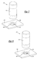
FIG. 1 is a schematic illustration of a first embodiment of the present invention of an arrangement for securing a MELF resistor to a leadframe; -
FIG. 2 is a terminal schematic illustration of the electronic component embodiment of the arrangement for securing the MELF resistor to the leadframe ofFig. 1 ; -
FIG. 3 is a third schematic illustration of the electronic component embodiment of the arrangement for securing the MELF resistor to the leadframe ofFigs. 1-2 ; -
FIG. 4 is a schematic illustration of a terminal embodiment of the present invention of an arrangement for securing a MELF resistor to a leadframe; -
FIG. 5 is a schematic illustration of a third embodiment of the present invention of an arrangement for securing a MELF resistor to a leadframe; -
FIG. 6 is a schematic illustration of a fourth embodiment of the present invention of an arrangement for securing a MELF resistor to a leadframe; -
FIG. 7 is a schematic illustration of a fifth embodiment of the present invention of an arrangement for securing a MELF resistor to a leadframe; and -
FIG. 8 is a schematic illustration of a sixth embodiment of the present invention of an arrangement for securing a MELF resistor to a leadframe. - The following description is merely exemplary in nature and is in no way intended to limit the disclosure, its application, or uses. For purposes of clarity, the same reference numbers will be used in the drawings to identify similar elements.
Figures 1-3 illustrate asensor assembly 10, preferably for an automotive vehicle. Theassembly 10 includes anelectronic component portion 12 and aterminal portion 14. Theelectronic component portion 12 may be any type of electronic component, such as a MELF (metal electrode leadless face) resistor or diode. Theterminal portion 14 may be any type of component which theelectronic component portion 12 needs to be secured, such as a leadframe or a PCB (printed circuit board). For example, theelectronic component portion 12 may be a MELF resistor sometimes used inengine speed sensors 10. - A receiving
location 16 is defined by theterminal portion 14. Thereceiving location 16 may be a through hole formed by punching or pierced in theterminal portion 14, or integrally formed when theterminal portion 14 is made. Alternately, thereceiving location 16 may be a marked location on theterminal portion 14, or an area where the material of theterminal portion 14 is thinner for easier deformation. Only a portion of theterminal portion 14 is shown, however, there may bemultiple receiving locations 16 located on onecomponent 14. - The
electronic component portion 12 is assembled to the terminal portion by pressing theelectronic component portion 12 into thereceiving location 16. The pressing operation for assembling theelectronic component portion 12 to theterminal portion 14 is faster and uses less material than the welding or soldering process of securing theelectronic component portion 12 to theleadframe 14. Additionally, the MELF style resistors or diodes are less expensive than leaded sensors. - When the
receiving location 16 is a through hole, the hole is preferably the size and geometry as is needed to provide a desired fit for a particularelectrical component 12. Theelectrical component 12 has a press fit or interference fit with theterminal portion 14. Excess material 18 is deformed when theelectrical component 12 is pressed into thereceiving location 16. - Referring to
Figures 4-8 several embodiments ofautomotive component assemblies electronic component portion terminal portion terminal portion location electrical component terminal portion excess material electrical component Phantom line electrical component receiving location excess material electrical component terminal portion receiving location excess material particular sensor assembly - Additionally, when assembled the
electrical component receiving location electronic component portion receiving location excess material electronic component portion terminal portion - While the best modes for carrying out the invention have been described in detail the true scope of the disclosure should not be so limited, since those familiar with the art to which this invention relates will recognize various alternative designs and embodiments for practicing the invention within the scope of the appended claims.
Claims (11)
- A sensor assembly comprising:a electronic component portion, wherein the electronic component portion is a metal electrode leadless face style component;a terminal portion, wherein the terminal portion defines a through hole and the electronic component portion is received within the through hole; andwherein the electronic component portion has a press fit with the terminal portion to retain the electronic component portion to the terminal portion.
- The sensor assembly of claim 1, wherein the terminal portion is a leadframe.
- The sensor assembly of claim 1, wherein the terminal portion is a printed circuit board.
- The sensor assembly of one of the claims 1-3, wherein the electronic component portion is a MELF resistor.
- The sensor assembly of one of the claims 1-4, wherein the sensor assembly is an engine speed sensor.
- A method of assembling sensor assembly comprising:forming a through hole in a terminal portion of the sensor assembly; andpressing an electronic component portion into the through hole defined by the terminal portion, wherein the electronic component portion has a press fit with the terminal portion, and wherein the electronic component portion is a metal electrode leadless face style component.
- The method of claim 6, wherein the terminal portion is a leadframe.
- The method of claim 6, wherein the terminal portion is a printed circuit board.
- The method of one of the claims 6-8, wherein the electronic component portion portion is a MELF resistor.
- The method of one of the claims 6-9, wherein the sensor assembly is an engine speed sensors.
- The method of one of the claims 6-10, wherein forming the hole further comprises one of punching and piercing the hole in the terminal portion.
Applications Claiming Priority (2)
| Application Number | Priority Date | Filing Date | Title |
|---|---|---|---|
| US201462061855P | 2014-10-09 | 2014-10-09 | |
| US14/878,457 US20160103146A1 (en) | 2014-10-09 | 2015-10-08 | Arrangement and method for connecting electronic components to a terminal for a sensor assembly |
Publications (2)
| Publication Number | Publication Date |
|---|---|
| EP3007524A2 true EP3007524A2 (en) | 2016-04-13 |
| EP3007524A3 EP3007524A3 (en) | 2016-08-03 |
Family
ID=54330595
Family Applications (1)
| Application Number | Title | Priority Date | Filing Date |
|---|---|---|---|
| EP15189102.5A Withdrawn EP3007524A3 (en) | 2014-10-09 | 2015-10-09 | Arrangement and method for connecting electronic components to a terminal for a sensor assembly |
Country Status (2)
| Country | Link |
|---|---|
| US (1) | US20160103146A1 (en) |
| EP (1) | EP3007524A3 (en) |
Families Citing this family (1)
| Publication number | Priority date | Publication date | Assignee | Title |
|---|---|---|---|---|
| CN106163111A (en) * | 2016-08-22 | 2016-11-23 | 常州鼎润电子科技有限公司 | Easily mounting circuit boards |
Citations (3)
| Publication number | Priority date | Publication date | Assignee | Title |
|---|---|---|---|---|
| US5990589A (en) * | 1996-12-13 | 1999-11-23 | Kabushiki Kaisha Sankyo Seiki Seisakusho | Brushless motor having core holder mounting to base board forming gap for wire insertion |
| US20080203835A1 (en) * | 2005-06-10 | 2008-08-28 | Jean-Marc Torres | Motor Drive Assembly |
| US20100313666A1 (en) * | 2008-01-11 | 2010-12-16 | Knorr Bremse Systeme Fuer Nutzfahrzeuge Gmbh | Conductor Track Carrier and Method for the Production of a Conductor Track Carrier |
Family Cites Families (12)
| Publication number | Priority date | Publication date | Assignee | Title |
|---|---|---|---|---|
| US4968269A (en) * | 1988-03-25 | 1990-11-06 | Cooper Industries, Inc. | Fuse holder |
| EP0359856B1 (en) * | 1988-04-09 | 1993-12-22 | Georg Sillner | Process and device for converting cylindrical electric components |
| US4970624A (en) * | 1990-01-22 | 1990-11-13 | Molex Incorporated | Electronic device employing a conductive adhesive |
| US5141455A (en) * | 1991-04-08 | 1992-08-25 | Molex Incorporated | Mounting of electronic components on substrates |
| DE9305285U1 (en) * | 1993-04-07 | 1993-06-09 | Ho, Yen Chung, Pan Chiao, Taipeh | Circuit board |
| JP2004505208A (en) * | 2000-07-27 | 2004-02-19 | ビステオン グローバル テクノロジーズ インコーポレイテッド | Integrated powertrain control system for large engines |
| US7304863B1 (en) * | 2003-06-09 | 2007-12-04 | Lattice Semiconductor Corporation | Integrated circuit including external electronic components with low insertion loss |
| US7863527B2 (en) * | 2007-02-23 | 2011-01-04 | Continental Automotive Systems Us, Inc. | Lead frame mount for circuit component |
| US7876577B2 (en) * | 2007-03-12 | 2011-01-25 | Tyco Electronics Corporation | System for attaching electronic components to molded interconnection devices |
| CN101978439B (en) * | 2008-02-22 | 2014-05-14 | 威世先进科技有限公司 | Surface mounted chip resistor with flexible leads |
| US8025508B2 (en) * | 2009-12-23 | 2011-09-27 | Hubbell Incorporated | Solar panel grounding connector |
| DE102010002943A1 (en) * | 2010-03-17 | 2011-09-22 | Robert Bosch Gmbh | Arrangement with an electrical and / or electronic module and a circuit carrier |
-
2015
- 2015-10-08 US US14/878,457 patent/US20160103146A1/en not_active Abandoned
- 2015-10-09 EP EP15189102.5A patent/EP3007524A3/en not_active Withdrawn
Patent Citations (3)
| Publication number | Priority date | Publication date | Assignee | Title |
|---|---|---|---|---|
| US5990589A (en) * | 1996-12-13 | 1999-11-23 | Kabushiki Kaisha Sankyo Seiki Seisakusho | Brushless motor having core holder mounting to base board forming gap for wire insertion |
| US20080203835A1 (en) * | 2005-06-10 | 2008-08-28 | Jean-Marc Torres | Motor Drive Assembly |
| US20100313666A1 (en) * | 2008-01-11 | 2010-12-16 | Knorr Bremse Systeme Fuer Nutzfahrzeuge Gmbh | Conductor Track Carrier and Method for the Production of a Conductor Track Carrier |
Also Published As
| Publication number | Publication date |
|---|---|
| EP3007524A3 (en) | 2016-08-03 |
| US20160103146A1 (en) | 2016-04-14 |
Similar Documents
| Publication | Publication Date | Title |
|---|---|---|
| EP2167930B1 (en) | Connection unit for a pressure measuring cell | |
| JP6230774B2 (en) | Ring-shaped or plate-shaped member and manufacturing method | |
| US11287449B2 (en) | Shunt resistor | |
| US10438730B2 (en) | Current sensing resistor and fabrication method thereof | |
| US20140213080A1 (en) | Press-fit pin, connection structure including the press-fit pin, and electronic device including the press-fit pin | |
| US10217594B2 (en) | Bridge assembly | |
| US8916079B2 (en) | Method for producing an electronic component | |
| DE69809379T2 (en) | pressure transducer | |
| DE102017125505A1 (en) | Socket for printed circuit boards | |
| US20160103146A1 (en) | Arrangement and method for connecting electronic components to a terminal for a sensor assembly | |
| JP2008541443A (en) | Particularly suitable for automotive instrument panels, a method for connecting to a printed circuit without soldering an electric drive | |
| DE102013202898B4 (en) | Sensor component for a pressure sensor | |
| US9030840B2 (en) | Arrangement comprising an electric and/or electronic module and a circuit carrier | |
| EP3007527A1 (en) | Arrangement and method for connecting an electrical component to a circuit portion | |
| JP2012099440A (en) | Holding member, and electronic component | |
| JP6307365B2 (en) | Terminal, terminal mounting structure, and electrical junction box comprising said terminal | |
| CN104668434A (en) | Method for producing an assembly unit | |
| JP2007087930A (en) | Threaded terminal | |
| JP5168440B2 (en) | Driving part fastening method and driving part | |
| CN103109422B (en) | Method for producing pin-shaped contact elements and contact element | |
| DE102015207873A1 (en) | Electronic module for a gearbox control unit | |
| CN104901041B (en) | Connecting pin for electronic circuit board | |
| EP3308873B1 (en) | Method of manufacturing a washer | |
| DE102006048068A1 (en) | fluid sensor | |
| WO2004068921A2 (en) | Electronic component |
Legal Events
| Date | Code | Title | Description |
|---|---|---|---|
| PUAI | Public reference made under article 153(3) epc to a published international application that has entered the european phase |
Free format text: ORIGINAL CODE: 0009012 |
|
| AK | Designated contracting states |
Kind code of ref document: A2 Designated state(s): AL AT BE BG CH CY CZ DE DK EE ES FI FR GB GR HR HU IE IS IT LI LT LU LV MC MK MT NL NO PL PT RO RS SE SI SK SM TR |
|
| AX | Request for extension of the european patent |
Extension state: BA ME |
|
| PUAL | Search report despatched |
Free format text: ORIGINAL CODE: 0009013 |
|
| AK | Designated contracting states |
Kind code of ref document: A3 Designated state(s): AL AT BE BG CH CY CZ DE DK EE ES FI FR GB GR HR HU IE IS IT LI LT LU LV MC MK MT NL NO PL PT RO RS SE SI SK SM TR |
|
| AX | Request for extension of the european patent |
Extension state: BA ME |
|
| RIC1 | Information provided on ipc code assigned before grant |
Ipc: H05K 1/18 20060101AFI20160624BHEP Ipc: H05K 3/32 20060101ALI20160624BHEP |
|
| STAA | Information on the status of an ep patent application or granted ep patent |
Free format text: STATUS: REQUEST FOR EXAMINATION WAS MADE |
|
| 17P | Request for examination filed |
Effective date: 20170203 |
|
| RBV | Designated contracting states (corrected) |
Designated state(s): AL AT BE BG CH CY CZ DE DK EE ES FI FR GB GR HR HU IE IS IT LI LT LU LV MC MK MT NL NO PL PT RO RS SE SI SK SM TR |
|
| STAA | Information on the status of an ep patent application or granted ep patent |
Free format text: STATUS: EXAMINATION IS IN PROGRESS |
|
| 17Q | First examination report despatched |
Effective date: 20200113 |
|
| STAA | Information on the status of an ep patent application or granted ep patent |
Free format text: STATUS: THE APPLICATION IS DEEMED TO BE WITHDRAWN |
|
| 18D | Application deemed to be withdrawn |
Effective date: 20200603 |