EP3007358A1 - Elastic wave filter device - Google Patents
Elastic wave filter device Download PDFInfo
- Publication number
- EP3007358A1 EP3007358A1 EP14804326.8A EP14804326A EP3007358A1 EP 3007358 A1 EP3007358 A1 EP 3007358A1 EP 14804326 A EP14804326 A EP 14804326A EP 3007358 A1 EP3007358 A1 EP 3007358A1
- Authority
- EP
- European Patent Office
- Prior art keywords
- elastic wave
- acoustic velocity
- width
- resonators
- low acoustic
- Prior art date
- Legal status (The legal status is an assumption and is not a legal conclusion. Google has not performed a legal analysis and makes no representation as to the accuracy of the status listed.)
- Granted
Links
Images



Classifications
-
- H—ELECTRICITY
- H03—ELECTRONIC CIRCUITRY
- H03H—IMPEDANCE NETWORKS, e.g. RESONANT CIRCUITS; RESONATORS
- H03H9/00—Networks comprising electromechanical or electro-acoustic elements; Electromechanical resonators
- H03H9/46—Filters
- H03H9/64—Filters using surface acoustic waves
- H03H9/6423—Means for obtaining a particular transfer characteristic
- H03H9/6433—Coupled resonator filters
- H03H9/6483—Ladder SAW filters
-
- H—ELECTRICITY
- H03—ELECTRONIC CIRCUITRY
- H03H—IMPEDANCE NETWORKS, e.g. RESONANT CIRCUITS; RESONATORS
- H03H9/00—Networks comprising electromechanical or electro-acoustic elements; Electromechanical resonators
- H03H9/02—Details
- H03H9/02535—Details of surface acoustic wave devices
- H03H9/02992—Details of bus bars, contact pads or other electrical connections for finger electrodes
-
- H—ELECTRICITY
- H03—ELECTRONIC CIRCUITRY
- H03H—IMPEDANCE NETWORKS, e.g. RESONANT CIRCUITS; RESONATORS
- H03H9/00—Networks comprising electromechanical or electro-acoustic elements; Electromechanical resonators
- H03H9/02—Details
- H03H9/125—Driving means, e.g. electrodes, coils
- H03H9/145—Driving means, e.g. electrodes, coils for networks using surface acoustic waves
-
- H—ELECTRICITY
- H03—ELECTRONIC CIRCUITRY
- H03H—IMPEDANCE NETWORKS, e.g. RESONANT CIRCUITS; RESONATORS
- H03H9/00—Networks comprising electromechanical or electro-acoustic elements; Electromechanical resonators
- H03H9/02—Details
- H03H9/125—Driving means, e.g. electrodes, coils
- H03H9/145—Driving means, e.g. electrodes, coils for networks using surface acoustic waves
- H03H9/14538—Formation
- H03H9/14541—Multilayer finger or busbar electrode
-
- H—ELECTRICITY
- H03—ELECTRONIC CIRCUITRY
- H03H—IMPEDANCE NETWORKS, e.g. RESONANT CIRCUITS; RESONATORS
- H03H9/00—Networks comprising electromechanical or electro-acoustic elements; Electromechanical resonators
- H03H9/02—Details
- H03H9/125—Driving means, e.g. electrodes, coils
- H03H9/145—Driving means, e.g. electrodes, coils for networks using surface acoustic waves
- H03H9/14544—Transducers of particular shape or position
- H03H9/1457—Transducers having different finger widths
-
- H—ELECTRICITY
- H03—ELECTRONIC CIRCUITRY
- H03H—IMPEDANCE NETWORKS, e.g. RESONANT CIRCUITS; RESONATORS
- H03H9/00—Networks comprising electromechanical or electro-acoustic elements; Electromechanical resonators
- H03H9/25—Constructional features of resonators using surface acoustic waves
-
- H—ELECTRICITY
- H03—ELECTRONIC CIRCUITRY
- H03H—IMPEDANCE NETWORKS, e.g. RESONANT CIRCUITS; RESONATORS
- H03H9/00—Networks comprising electromechanical or electro-acoustic elements; Electromechanical resonators
- H03H9/46—Filters
- H03H9/64—Filters using surface acoustic waves
- H03H9/6423—Means for obtaining a particular transfer characteristic
- H03H9/6426—Combinations of the characteristics of different transducers
-
- H—ELECTRICITY
- H03—ELECTRONIC CIRCUITRY
- H03H—IMPEDANCE NETWORKS, e.g. RESONANT CIRCUITS; RESONATORS
- H03H9/00—Networks comprising electromechanical or electro-acoustic elements; Electromechanical resonators
- H03H9/46—Filters
- H03H9/64—Filters using surface acoustic waves
- H03H9/6489—Compensation of undesirable effects
- H03H9/6496—Reducing ripple in transfer characteristic
-
- H—ELECTRICITY
- H03—ELECTRONIC CIRCUITRY
- H03H—IMPEDANCE NETWORKS, e.g. RESONANT CIRCUITS; RESONATORS
- H03H9/00—Networks comprising electromechanical or electro-acoustic elements; Electromechanical resonators
- H03H9/0004—Impedance-matching networks
- H03H9/0009—Impedance-matching networks using surface acoustic wave devices
-
- H—ELECTRICITY
- H03—ELECTRONIC CIRCUITRY
- H03H—IMPEDANCE NETWORKS, e.g. RESONANT CIRCUITS; RESONATORS
- H03H9/00—Networks comprising electromechanical or electro-acoustic elements; Electromechanical resonators
- H03H9/46—Filters
- H03H9/64—Filters using surface acoustic waves
- H03H9/6423—Means for obtaining a particular transfer characteristic
- H03H9/6433—Coupled resonator filters
Definitions
- the present invention relates to elastic wave filter devices configured by connecting a plurality of elastic wave resonators, and particularly relates to elastic wave filter devices including serial and parallel arms.
- Patent Document 1 and Patent Document 2 cited below disclose a structure in which an acoustic velocity in an electrode finger leading end-side portion is lower than an acoustic velocity in an electrode finger intersecting portion in an IDT (interdigital transducer) electrode. It is discussed that a piston mode is formed by using the above structure so that ripples due to transverse modes can be suppressed.
- Patent Document 1 discloses that the width of an opening, areas in which acoustic velocities differ from each other, and so on in a serial arm resonator are set to be different from the width of an opening, areas in which acoustic velocities differ from each other, and so on in a parallel arm resonator.
- Patent Document 3 discloses a ladder filter in which an intersecting width of a parallel arm resonator is larger than an intersecting width of a serial arm resonator. With this structure, it is expected to suppress spurious response caused by transverse modes and to realize miniaturization. Making the intersecting width of the parallel arm resonator larger increases transverse mode harmonics. It is discussed that the increase in the transverse mode harmonics disperses the transverse mode spurious response.
- Patent Documents 1 and 2 disclose a configuration in which transverse mode ripples are suppressed by forming a piston mode.
- the width of the opening, shapes of the areas in which acoustic velocities differ from each other, and so on are set to be different between the serial arm resonator and the parallel arm resonator.
- the suppression of transverse mode ripples cannot be realized with certainty only by simply setting the width of the opening, the areas in which acoustic velocities differ from each other, and so on to be different between the serial arm resonator and the parallel arm resonator.
- An object of the present invention is to provide an elastic wave filter device capable of suppressing transverse mode ripples with certainty.
- An elastic wave filter device includes a serial arm connecting an input terminal to an output terminal and a parallel arm connecting the serial arm to a ground potential, and also includes a plurality of elastic wave resonators.
- each of the elastic wave resonators includes a piezoelectric substrate and an IDT electrode formed on the piezoelectric substrate.
- the IDT electrode includes a first busbar, a second busbar disposed being spaced from the first busbar, a plurality of first electrode fingers, each base end of which is electrically connected to the first busbar, that extend toward the second busbar side, and a plurality of second electrode fingers, each base end of which is electrically connected to the second bus bar, that extend toward the first busbar side and are interleaved with the plurality of first electrode fingers.
- a central area at a center in a direction in which the first and second electrode fingers of the IDT electrode extend a low acoustic velocity area at an outer side portion of the central area in a direction in which the electrode fingers extend where an acoustic velocity is relatively low in comparison with the central area, and a high acoustic velocity area at an outer side portion in a direction in which the low acoustic velocity area extends where an elastic wave propagation velocity is higher than an elastic wave propagation velocity in the central area.
- a dimension of the low acoustic velocity area in the width direction of at least one elastic wave resonator differs from a dimension of the low acoustic velocity area in the width direction of the other elastic wave resonators.
- the first and second busbars respectively have a plurality of cavities arranged in a dispersed manner along the elastic wave propagation direction.
- An inner side portion relative to the cavities in the width direction of the IDT electrode is taken as an inner side busbar section, a portion where the plurality of cavities are provided is taken as a central busbar section, and an outer side portion relative to the central busbar section is taken as an outer side busbar section.
- the inner side busbar section is formed in a belt-like shape extending in the elastic wave propagation direction, and the central busbar section configures the aforementioned high acoustic velocity area.
- the inner side busbar width and/or a wide width portion provided on the base end side relative to the central area are included, and the inner side busbar width and/or a width of the wide width portion differ between at least the one elastic wave resonator and the other elastic wave resonators.
- a ladder filter is configured including a serial arm resonator (wherein a plurality of elastic wave resonators are provided in the serial arm) and a parallel arm resonator (wherein a plurality of elastic wave resonators are also provided in the parallel arm), in which at least the "one" elastic wave resonator corresponds to the serial arm resonator and the "other" elastic wave resonators correspond to the parallel arm resonator.
- a dimension of a low acoustic velocity area in the width direction of the serial arm resonator is smaller than a dimension of a low acoustic velocity area in the width direction of the parallel arm resonator.
- the serial arm resonator includes a plurality of resonators and the parallel arm resonator also includes a plurality of resonators, and the dimension of each low acoustic velocity area in the width direction of the plurality of serial arm resonators is smaller than the dimension of each low acoustic velocity area in the width direction of the plurality of parallel arm resonators.
- the dimension of the low acoustic velocity area in the width direction of at least one of the plurality of serial arm resonators differs from the dimension of the low acoustic velocity area in the width direction of the other serial arm resonators.
- the dimension of the low acoustic velocity area in the width direction of at least one of the plurality of parallel arm resonators differs from the dimension of the low acoustic velocity area in the width direction of the other parallel arm resonators.
- the low acoustic velocity area includes the inner side busbar width and/or the wide width portion provided on the base end side relative to the central area, and the inner side busbar width and/or the width of the wide width portion are smaller in the serial arm resonator than in the parallel arm resonator.
- the width of a low acoustic velocity area in at least one elastic wave resonator differs from the width of each low acoustic velocity area in the other elastic wave resonators, transverse mode ripples can be effectively suppressed.
- Fig. 2 is a circuit diagram of an elastic wave filter device according to a first embodiment of the present invention.
- the elastic wave filter device 1 is a ladder filter. Note that, however, the present invention is not limited to a ladder filter, as described later.
- the elastic wave filter device 1 includes a serial arm 4 connecting an input terminal 2 to an output terminal 3. There are provided first through third parallel arms 5, 6, and 7 that connect the serial arm 4 to a ground potential. A plurality of serial arm resonators S1-1, S1-2, S1-3, S2-1, S2-2, S2-3, S3-1, S3-2, and S3-3 are arranged in the serial arm 4. A capacitor C1 is connected in parallel to the serial arm resonators S2-2 and S2-3.
- the parallel arm 5 connects a connection point between the serial arm resonators S1-3 and S2-1 to the ground potential.
- a parallel arm resonator P1 and an inductance L1 are connected in series.
- the second parallel arm 6 is connected to a connection point between the serial arm resonators S2-3 and S3-1.
- the third parallel arm 7 is connected to the output terminal 3.
- a parallel arm resonator P2 is disposed in the second parallel arm 6, and a parallel arm resonator P3 is disposed in the third parallel arm 7.
- the second parallel arm 6 and the third parallel arm 7 are connected to each other with a shared connection point 8, and an inductance L2 is connected between the shared connection point 8 and the ground potential.
- the serial arm resonators S1-1 through S3-3 and the parallel arm resonators P1 through P3 are respectively configured of surface acoustic wave resonators.
- the surface acoustic wave resonator has a structure in which an IDT electrode is formed on a piezoelectric substrate, as widely known.
- Fig. 3(a) and Fig. 3(b) are a schematic plan view of the serial arm resonator S1-1 and an enlarged cross-sectional view illustrating an electrode structure of the stated resonator, respectively.
- the serial arm resonator S1-1 includes a piezoelectric substrate 11 and an IDT electrode 12 formed on the piezoelectric substrate 11. Reflectors 13 and 14 are provided on both sides of the IDT electrode 12 in a propagation direction of the surface acoustic wave.
- the serial arm resonator S1-1 is a one-port type surface acoustic wave resonator having the above-described structure.
- a film of SiO 2 and a film of SiN are laminated as dielectric layers so as to cover the IDT electrode 12 and the reflectors 13 and 14.
- Fig. 3(b) illustrates the above lamination structure in an enlarged manner.
- the piezoelectric substrate 11 is formed with LiNbO 3 of 127.5° Y-X.
- the material for forming the piezoelectric substrate is not limited to any specific one. In other words, various types of piezoelectric single crystals or piezoelectric ceramics can be used.
- Fig. 3 (b) illustrates, in an enlarged manner, a portion where a single electrode finger of the IDT electrode 12 is formed.
- the IDT electrode 12 is formed on the piezoelectric substrate 11.
- the IDT electrode 12 is formed of laminated metal films in the present embodiment.
- the stated electrode has a structure in which a NiCr film 12a, a Pt film 12b, a Ti film 12c, an AlCu film 12d, and a Ti film 12e are laminated in that order from bottom.
- the thicknesses of the respective layers are as follows: that is, NiCr film 12a: 100 ⁇ ; Pt film 12b: 360 ⁇ ; Ti film 12c: 100 ⁇ ; AlCu film 12d: 1500 ⁇ ; Ti film 12e: 100 ⁇ .
- a SiO 2 film 15 is so laminated as to cover the IDT electrode 12.
- a thickness as a dimension of the SiO 2 film 15 from an upper surface of the piezoelectric substrate 11 up to an upper surface of the SiO 2 film 15 is 5700 ⁇ .
- a SiN film 16 is laminated on the SiO 2 film 15. The SiN film 16 is 200 ⁇ in thickness.
- the structure of the surface acoustic wave resonator has been described, while taking the serial arm resonator S1-1 as a representative. Note that the other serial arm resonators S1-2 through S3-3 and the parallel arm resonators P1 through P3 are also configured of the same one-port type surface acoustic wave resonator. Further, the electrode structure, the dielectric layer thickness, and so on of each of the surface acoustic wave resonators are set to be the same as those of the serial arm resonator S1-1.
- a low acoustic velocity area and a high acoustic velocity area are provided in each surface acoustic wave resonator of the serial arm resonators S1-1 through S3-3 and the parallel arm resonators P1 through P3.
- the following low and high acoustic velocity areas are provided. This will be more specifically described below with reference to Figs. 1(a) and 1(b) .
- Fig. 1(a) is an enlarged partial cutout plan view illustrating the principal portion of the IDT electrode of the serial arm resonator S3-1.
- the IDT electrode includes a first busbar 21.
- a second busbar side is omitted.
- the second busbar side is configured in the same manner as the first busbar side.
- the busbar 21 includes an inner side busbar section 21A, a central busbar section 21B, and an outer side busbar section 21C.
- inner side refers to a side of an area where first and second electrode fingers 23 and 24 intersect with each other.
- a base end of the first electrode finger 23 is connected to the first busbar 21.
- a base end of the second electrode finger 24 is connected to the second busbar (not shown).
- a cavity 25 is provided in the central busbar section 21B.
- the cavity 25 is formed in a rectangular shape in the present embodiment. Note that, however, the shape of the cavity 25 is not limited to any specific one. Providing the cavity 25 allows an acoustic velocity in the central busbar section 21B, where the stated cavity 25 is provided, to be higher as represented by "V 3 ".
- the area where the central busbar section 21B is provided constitutes a high acoustic velocity area.
- the inner side busbar section 21A is a busbar portion having an elongate belt-like shape. As such, since this busbar section is a metallized area, a low acoustic velocity area is configured therein. Further, the base end side portion of the first finger electrode 23 includes a convex portion 23a and a plurality of wide width portions 23b having width-direction projections. A wide width portion 24a is also provided at a leading end side of the second electrode finger 24. As such, since the wide width portions 23b and 24a are provided, this area configures a low acoustic velocity area.
- a central portion of an area where the first electrode finger 23 and the second electrode finger 24 intersect with each other in the width direction is a central area represented by an acoustic velocity V 1 .
- the low acoustic velocity area is positioned at the outer side portion of the central area
- the high acoustic velocity area is positioned at the outer side portion of the low acoustic velocity area.
- the acoustic velocity in the central area is V 1
- the acoustic velocity in the low acoustic velocity area is V 2 A
- the acoustic velocity in the high acoustic velocity area is V 3 .
- a width of the low acoustic velocity area is W1A
- a width of the high acoustic velocity area is W2.
- the width of the low acoustic velocity area of the serial arm resonator S3-1 is W1A, and a width of each low acoustic velocity area of the serial arm resonators S3-2 and S3-3 is also W1A, which is the same in dimension as that of the serial arm resonator S3-1.
- Fig. 1(b) is a view illustrating the principal portion of the IDT electrode of the parallel resonator P1 in the present embodiment.
- the electrode structure of the parallel arm resonator P1 is substantially the same as that of the serial arm resonator S3-1 shown in Fig. 1(a) . Note that, however, a width W1B of the low acoustic velocity area is larger than the width W1A of the low acoustic velocity area shown in Fig. 1(a) .
- the width W1A of the low acoustic velocity area of the serial arm resonators S3-1 through S3-3 is smaller than the width W1B of the low acoustic velocity area of the parallel arm resonator P1.
- the width W1B of the above low acoustic velocity area is larger than the width of the low acoustic velocity area of the other parallel arm resonators P2 and P3, and also larger than the width of the low acoustic velocity area of the serial arm resonators S1-1 through S3-3.
- the width W1A of the low acoustic velocity area of the serial arm resonators S3-1 through S3-3 is made smaller than the width of the low acoustic velocity area of the other resonators, transverse mode ripples can be effectively suppressed in the pass band. This will be explained hereinafter based on a specific experiment example.
- Table 1 shown below, indicated are design parameters of the serial arm resonators S1-1 through S3-3 and the parallel arm resonators P1 through P3 of the present embodiment.
- Table 1 P1 S1-1 S1-2 S1-3 P2 S2-1 S2-2 S2-3 P3 S3-1 S3-2 S3-3 IDT Wavelength ( ⁇ m) 2.150 2.040 2.040 2.040 2.137 2.043 2.042 2.034 2.113 2.033 2.033 2.033 Intersecting Width ( ⁇ m) 48 38 38 38 38 53 42 41 31 61 34 34 29 Number of Pairs 87 171 171 171 97 189 188 139 110 152 133 Duty 0.475 0.475 0.475 0.475 0.475 0.475 0.475 0.475 0.475 0.475 0.475 0.475 0.475 0.475 0.475 0.475 0.475 0.475 0.475 0.475 0.475 0.475 0.475 0.475 0.475 0.475 0.475 0.475 0.475 0.475 0.475 0.475 0.4
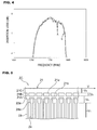
- a solid line represents attenuation frequency characteristics of the elastic wave filter device 1 of the present embodiment.
- a broken line represents a result of a comparative example in which widths of the low acoustic velocity areas are the same in all the resonators and widths of the high acoustic velocity areas are also the same in all the resonators.
- a dot-dash line represents attenuation frequency characteristics of a second embodiment, which will be explained later.
- the transverse mode ripple indicated by the arrow A is a ripple caused by the serial arm resonators S3-1 through S3-3.
- the pass band is defined by an anti-resonant frequency of a parallel arm resonator and a resonant frequency of a serial arm resonator. Accordingly, in the case where a transverse mode remains in the vicinity of the anti-resonant frequency of the parallel arm resonator and the vicinity of the resonant frequency of the serial arm resonator, a ripple is generated within the pass band.
- the low acoustic velocity areas of all the resonators are the same in dimension and the high acoustic velocity areas of all the resonators are also the same in dimension.
- transverse mode ripples cannot be completely suppressed in all the resonators.
- This allows transverse mode ripples to be generated within the pass band. Accordingly, there arises a problem that the loss is worsened within the pass band.
- the transverse mode ripple is generated within the pass band caused by the serial arm resonators S3-1, S3-2, and S3-3.
- the ripple indicated by the arrow A is generated by the serial arm resonators S3-1 through S3-3.
- the transverse mode ripple indicated by the arrow A does not appear. This is because, as mentioned earlier, the width W1A of the low acoustic velocity area in the serial arm resonators S3-1 through S3-3 is smaller than the width of the low acoustic velocity area in the other serial arm resonators S1-1 through S2-3. In other words, because transverse mode ripples in S3-1 through S3-3 can be reduced by making the width of the low acoustic velocity area smaller, it is understood that the ripple indicated by the arrow A within the pass band can be suppressed.
- the width W1B of the low acoustic velocity area in the parallel arm resonator P1 is made larger than the width of the low acoustic velocity area in the other parallel arm resonators P2 and P3, and also larger than the width of the low acoustic velocity area in the serial arm resonators S1-1 through S1-3. Accordingly, the transverse mode ripple indicated by the arrow B is also suppressed.
- the dot-dash line represents the attenuation frequency characteristics of an elastic wave filter device as the second embodiment configured in the same manner as the elastic wave filter device of the above embodiment except that the width of the low acoustic velocity area of the serial arm resonators S3-1 through S3-3 is the same as that of the serial arm resonators S1-1 through S2-3.
- the width of the low acoustic velocity area of the serial arm resonators S1-1 through S3-3 is made smaller than the width of the low acoustic velocity area of the parallel arm resonators P1 through P3.
- the width W1A of the low acoustic velocity area in the serial arm resonators S3-1 through S3-3 be smaller than the width of the low acoustic velocity area in the other serial arm resonators S1-1 through S2-3.
- the width of the low acoustic velocity area in the serial arm resonators S1-1 through S3-3 be smaller than the width of the low acoustic velocity area in the parallel arm resonators P1 through P3.
- the present invention is not limited to the elastic wave filter device having the ladder circuit configuration as described in the above embodiments.
- the invention can be applied to various types of filter devices that include serial and parallel arms and a plurality of elastic wave resonators.
- the invention may be applied to a filter device including serial and parallel arms, where elastic wave resonators are disposed in the plurality of parallel arms but not disposed in the serial arm.
- the invention may be applied to a filter device in which, conversely, a plurality of elastic wave resonators are connected to the serial arm in series to each other while the parallel arms do not have any elastic wave resonator.
- the invention may be applied to an elastic wave filter device in which the serial arm includes one elastic wave resonator and the parallel arm includes another elastic wave resonator.
- ripples within the band can be suppressed in accordance with the present invention.
- it is more effective to shorten the width of the low acoustic velocity area in the elastic wave resonator disposed in the serial arm than to shorten the width of the low acoustic velocity area in the elastic wave resonator disposed in the parallel arm. By doing so, ripples within the pass band can be effectively suppressed.
- the elastic wave resonator used in the present invention may be a surface acoustic wave resonator making use of the aforementioned surface acoustic waves, or may be an elastic wave resonator making use of other elastic waves such as boundary acoustic waves or the like.
- an arbitrary elastic wave resonator having an IDT electrode can be used.
- the width of the low acoustic velocity area can be changed in various modes.
- the change of the above-mentioned width can be made by changing the dimension in the width direction of the area where the wide width portion 23b is provided, the width of the belt-like busbar portion configuring the inner side busbar section 21A, or the like.
- the invention is not limited to the configuration shown in Fig. 1(a) where the plurality of wide width portions are provided at the leading end side and the base end side of the electrode fingers; a configuration in which a single wide width portion 24a is provided at the leading end side of the second electrode finger 24, like an elastic wave resonator 51 shown in Fig. 5 , may be employed.
- the wide width portion may not be provided on the first and second finger electrodes 23 and 24, and the low acoustic velocity area may be formed only with the inner side busbar section 21A.
- adjusting the width of the inner side busbar section 21A makes it possible to adjust the width of the low acoustic velocity area.
Landscapes
- Physics & Mathematics (AREA)
- Acoustics & Sound (AREA)
- Surface Acoustic Wave Elements And Circuit Networks Thereof (AREA)
Abstract
Description
- The present invention relates to elastic wave filter devices configured by connecting a plurality of elastic wave resonators, and particularly relates to elastic wave filter devices including serial and parallel arms.
- A variety of filter devices including serial and parallel arm resonators configured of surface acoustic wave resonators have been proposed. For example, Patent Document 1 and
Patent Document 2 cited below disclose a structure in which an acoustic velocity in an electrode finger leading end-side portion is lower than an acoustic velocity in an electrode finger intersecting portion in an IDT (interdigital transducer) electrode. It is discussed that a piston mode is formed by using the above structure so that ripples due to transverse modes can be suppressed. - Further, Patent Document 1 discloses that the width of an opening, areas in which acoustic velocities differ from each other, and so on in a serial arm resonator are set to be different from the width of an opening, areas in which acoustic velocities differ from each other, and so on in a parallel arm resonator.
-
Patent Document 3 cited below discloses a ladder filter in which an intersecting width of a parallel arm resonator is larger than an intersecting width of a serial arm resonator. With this structure, it is expected to suppress spurious response caused by transverse modes and to realize miniaturization. Making the intersecting width of the parallel arm resonator larger increases transverse mode harmonics. It is discussed that the increase in the transverse mode harmonics disperses the transverse mode spurious response. -
- Patent Document 1:
WO 2011/088904 A1 - Patent Document 2:
Japanese Unexamined Patent Application Publication No. 2011-101350 - Patent Document 3:
Japanese Unexamined Patent Application Publication No. 2011-205625 -
Patent Documents 1 and 2 disclose a configuration in which transverse mode ripples are suppressed by forming a piston mode. In particular, it is disclosed in Patent Document 1 that the width of the opening, shapes of the areas in which acoustic velocities differ from each other, and so on are set to be different between the serial arm resonator and the parallel arm resonator. However, the suppression of transverse mode ripples cannot be realized with certainty only by simply setting the width of the opening, the areas in which acoustic velocities differ from each other, and so on to be different between the serial arm resonator and the parallel arm resonator. - Furthermore, it is difficult to sufficiently suppress transverse mode ripples only by simply changing the intersecting width as disclosed in
Patent Document 3. - An object of the present invention is to provide an elastic wave filter device capable of suppressing transverse mode ripples with certainty.
- An elastic wave filter device according to the present invention includes a serial arm connecting an input terminal to an output terminal and a parallel arm connecting the serial arm to a ground potential, and also includes a plurality of elastic wave resonators. In the present invention, each of the elastic wave resonators includes a piezoelectric substrate and an IDT electrode formed on the piezoelectric substrate.
- In the present invention, the IDT electrode includes a first busbar, a second busbar disposed being spaced from the first busbar, a plurality of first electrode fingers, each base end of which is electrically connected to the first busbar, that extend toward the second busbar side, and a plurality of second electrode fingers, each base end of which is electrically connected to the second bus bar, that extend toward the first busbar side and are interleaved with the plurality of first electrode fingers.
- Further, there are provided a central area at a center in a direction in which the first and second electrode fingers of the IDT electrode extend, a low acoustic velocity area at an outer side portion of the central area in a direction in which the electrode fingers extend where an acoustic velocity is relatively low in comparison with the central area, and a high acoustic velocity area at an outer side portion in a direction in which the low acoustic velocity area extends where an elastic wave propagation velocity is higher than an elastic wave propagation velocity in the central area. In the present invention, in the case where a direction orthogonal to an elastic wave propagation direction is taken as a width direction, a dimension of the low acoustic velocity area in the width direction of at least one elastic wave resonator differs from a dimension of the low acoustic velocity area in the width direction of the other elastic wave resonators.
- In a specific aspect of the elastic wave filter device according to the present invention, the first and second busbars respectively have a plurality of cavities arranged in a dispersed manner along the elastic wave propagation direction. An inner side portion relative to the cavities in the width direction of the IDT electrode is taken as an inner side busbar section, a portion where the plurality of cavities are provided is taken as a central busbar section, and an outer side portion relative to the central busbar section is taken as an outer side busbar section. The inner side busbar section is formed in a belt-like shape extending in the elastic wave propagation direction, and the central busbar section configures the aforementioned high acoustic velocity area.
- In further another specific aspect of the elastic wave filter device according to the present invention, the inner side busbar width and/or a wide width portion provided on the base end side relative to the central area are included, and the inner side busbar width and/or a width of the wide width portion differ between at least the one elastic wave resonator and the other elastic wave resonators.
- In another specific aspect of the elastic wave filter device according to the present invention, a ladder filter is configured including a serial arm resonator (wherein a plurality of elastic wave resonators are provided in the serial arm) and a parallel arm resonator (wherein a plurality of elastic wave resonators are also provided in the parallel arm), in which at least the "one" elastic wave resonator corresponds to the serial arm resonator and the "other" elastic wave resonators correspond to the parallel arm resonator.
- In still another specific aspect of the elastic wave filter device according to the present invention, a dimension of a low acoustic velocity area in the width direction of the serial arm resonator is smaller than a dimension of a low acoustic velocity area in the width direction of the parallel arm resonator.
- In still another specific aspect of the elastic wave filter device according to the present invention, the serial arm resonator includes a plurality of resonators and the parallel arm resonator also includes a plurality of resonators, and the dimension of each low acoustic velocity area in the width direction of the plurality of serial arm resonators is smaller than the dimension of each low acoustic velocity area in the width direction of the plurality of parallel arm resonators.
- In still another specific aspect of the elastic wave filter device according to the present invention, the dimension of the low acoustic velocity area in the width direction of at least one of the plurality of serial arm resonators differs from the dimension of the low acoustic velocity area in the width direction of the other serial arm resonators.
- In still another specific aspect of the elastic wave filter device according to the present invention, the dimension of the low acoustic velocity area in the width direction of at least one of the plurality of parallel arm resonators differs from the dimension of the low acoustic velocity area in the width direction of the other parallel arm resonators.
- In still another specific aspect of the elastic wave filter device according to the present invention, the low acoustic velocity area includes the inner side busbar width and/or the wide width portion provided on the base end side relative to the central area, and the inner side busbar width and/or the width of the wide width portion are smaller in the serial arm resonator than in the parallel arm resonator.
- In the elastic wave filter device according to the present invention, because the width of a low acoustic velocity area in at least one elastic wave resonator differs from the width of each low acoustic velocity area in the other elastic wave resonators, transverse mode ripples can be effectively suppressed.
-
- [
Fig. 1] Fig. 1(a) and Fig. 1(b) are an enlarged partial cutout plan view illustrating the principal portion of an IDT electrode of a single serial arm resonator and an enlarged partial cutout plan view illustrating the principal portion of an IDT electrode of a single parallel arm resonator, respectively, in an elastic wave filter device according to a first embodiment of the present invention. - [
Fig. 2] Fig. 2 is a circuit diagram of the elastic wave filter device according to the first embodiment of the present invention. - [
Fig. 3] Fig. 3(a) and Fig. 3(b) are a schematic plan view of a serial arm resonator S1-1 and an enlarged cross-sectional view illustrating an electrode structure of the stated resonator, respectively, in the elastic wave filter device according to the first embodiment of the present invention. - [
Fig. 4] Fig. 4 is a diagram illustrating respective filter characteristics of the elastic wave filter device according to the first embodiment, an elastic wave filter device according to a second embodiment of the present invention, and an elastic wave filter device according to a comparative example. - [
Fig. 5] Fig. 5 is a partial cutout plan view illustrating a variation on a planar shape of an elastic wave resonator IDT electrode used in an elastic wave resonator that is used in an elastic wave filter device according to the present invention. - [
Fig. 6] Fig. 6 is a partial cutout plan view illustrating another variation on a planar shape of an elastic wave resonator IDT electrode used in an elastic wave resonator that is used in an elastic wave filter device according to the present invention. - Hereinafter, the present invention will be clarified through description of specific embodiments of the invention with reference to the drawings.
-
Fig. 2 is a circuit diagram of an elastic wave filter device according to a first embodiment of the present invention. The elastic wave filter device 1 is a ladder filter. Note that, however, the present invention is not limited to a ladder filter, as described later. - The elastic wave filter device 1 includes a serial arm 4 connecting an
input terminal 2 to anoutput terminal 3. There are provided first through thirdparallel arms - The
parallel arm 5 connects a connection point between the serial arm resonators S1-3 and S2-1 to the ground potential. In theparallel arm 5, a parallel arm resonator P1 and an inductance L1 are connected in series. - The second
parallel arm 6 is connected to a connection point between the serial arm resonators S2-3 and S3-1. The thirdparallel arm 7 is connected to theoutput terminal 3. - A parallel arm resonator P2 is disposed in the second
parallel arm 6, and a parallel arm resonator P3 is disposed in the thirdparallel arm 7. The secondparallel arm 6 and the thirdparallel arm 7 are connected to each other with a shared connection point 8, and an inductance L2 is connected between the shared connection point 8 and the ground potential. - In the elastic wave filter device 1, the serial arm resonators S1-1 through S3-3 and the parallel arm resonators P1 through P3 are respectively configured of surface acoustic wave resonators.
- The surface acoustic wave resonator has a structure in which an IDT electrode is formed on a piezoelectric substrate, as widely known.
-
Fig. 3(a) and Fig. 3(b) are a schematic plan view of the serial arm resonator S1-1 and an enlarged cross-sectional view illustrating an electrode structure of the stated resonator, respectively. - As shown in
Fig. 3(a) , the serial arm resonator S1-1 includes apiezoelectric substrate 11 and anIDT electrode 12 formed on thepiezoelectric substrate 11.Reflectors IDT electrode 12 in a propagation direction of the surface acoustic wave. The serial arm resonator S1-1 is a one-port type surface acoustic wave resonator having the above-described structure. Although not illustrated inFig. 3(a) , a film of SiO2 and a film of SiN are laminated as dielectric layers so as to cover theIDT electrode 12 and thereflectors -
Fig. 3(b) illustrates the above lamination structure in an enlarged manner. In the present embodiment, thepiezoelectric substrate 11 is formed with LiNbO3 of 127.5° Y-X. In the present invention, however, the material for forming the piezoelectric substrate is not limited to any specific one. In other words, various types of piezoelectric single crystals or piezoelectric ceramics can be used. -
Fig. 3 (b) illustrates, in an enlarged manner, a portion where a single electrode finger of theIDT electrode 12 is formed. TheIDT electrode 12 is formed on thepiezoelectric substrate 11. TheIDT electrode 12 is formed of laminated metal films in the present embodiment. In other words, the stated electrode has a structure in which aNiCr film 12a, aPt film 12b, aTi film 12c, anAlCu film 12d, and aTi film 12e are laminated in that order from bottom. In the present embodiment, the thicknesses of the respective layers are as follows: that is,NiCr film 12a: 100 Å;Pt film 12b: 360 Å;Ti film 12c: 100 Å;AlCu film 12d: 1500 Å;Ti film 12e: 100 Å. Note that a SiO2 film 15 is so laminated as to cover theIDT electrode 12. A thickness as a dimension of the SiO2 film 15 from an upper surface of thepiezoelectric substrate 11 up to an upper surface of the SiO2 film 15 is 5700 Å. ASiN film 16 is laminated on the SiO2 film 15. TheSiN film 16 is 200 Å in thickness. - It is not absolutely necessary to provide the SiO2 film 15 and the
SiN film 16 as the dielectric layers. - The structure of the surface acoustic wave resonator has been described, while taking the serial arm resonator S1-1 as a representative. Note that the other serial arm resonators S1-2 through S3-3 and the parallel arm resonators P1 through P3 are also configured of the same one-port type surface acoustic wave resonator. Further, the electrode structure, the dielectric layer thickness, and so on of each of the surface acoustic wave resonators are set to be the same as those of the serial arm resonator S1-1.
- In the elastic wave filter device 1 of the present embodiment, a low acoustic velocity area and a high acoustic velocity area are provided in each surface acoustic wave resonator of the serial arm resonators S1-1 through S3-3 and the parallel arm resonators P1 through P3. In order to suppress transverse mode ripples by using a piston mode, the following low and high acoustic velocity areas are provided. This will be more specifically described below with reference to
Figs. 1(a) and 1(b) . -
Fig. 1(a) is an enlarged partial cutout plan view illustrating the principal portion of the IDT electrode of the serial arm resonator S3-1. In the serial arm resonator S3-1, the IDT electrode includes afirst busbar 21. InFig. 1(a) , only thefirst busbar 21 side is illustrated whereas a second busbar side is omitted. However, it is to be noted that the second busbar side is configured in the same manner as the first busbar side. - In the IDT electrode, a direction orthogonal to the surface acoustic wave propagation direction (or a direction in which the electrode fingers extend) is referred to as a width direction. The
busbar 21 includes an innerside busbar section 21A, acentral busbar section 21B, and an outerside busbar section 21C. Here, the term "inner side" refers to a side of an area where first andsecond electrode fingers - A base end of the
first electrode finger 23 is connected to thefirst busbar 21. A base end of thesecond electrode finger 24 is connected to the second busbar (not shown). - In the
first busbar 21, acavity 25 is provided in thecentral busbar section 21B. Thecavity 25 is formed in a rectangular shape in the present embodiment. Note that, however, the shape of thecavity 25 is not limited to any specific one. Providing thecavity 25 allows an acoustic velocity in thecentral busbar section 21B, where the statedcavity 25 is provided, to be higher as represented by "V3". The area where thecentral busbar section 21B is provided constitutes a high acoustic velocity area. - The inner
side busbar section 21A is a busbar portion having an elongate belt-like shape. As such, since this busbar section is a metallized area, a low acoustic velocity area is configured therein. Further, the base end side portion of thefirst finger electrode 23 includes aconvex portion 23a and a plurality ofwide width portions 23b having width-direction projections. Awide width portion 24a is also provided at a leading end side of thesecond electrode finger 24. As such, since thewide width portions - Meanwhile, a central portion of an area where the
first electrode finger 23 and thesecond electrode finger 24 intersect with each other in the width direction is a central area represented by an acoustic velocity V1. - In other words, in the serial arm resonator S3-1, the low acoustic velocity area is positioned at the outer side portion of the central area, and the high acoustic velocity area is positioned at the outer side portion of the low acoustic velocity area. The acoustic velocity in the central area is V1, the acoustic velocity in the low acoustic velocity area is V2A, and the acoustic velocity in the high acoustic velocity area is V3. Further, a width of the low acoustic velocity area is W1A, and a width of the high acoustic velocity area is W2.
- In the present embodiment, the width of the low acoustic velocity area of the serial arm resonator S3-1 is W1A, and a width of each low acoustic velocity area of the serial arm resonators S3-2 and S3-3 is also W1A, which is the same in dimension as that of the serial arm resonator S3-1.
- On the other hand,
Fig. 1(b) is a view illustrating the principal portion of the IDT electrode of the parallel resonator P1 in the present embodiment. The electrode structure of the parallel arm resonator P1 is substantially the same as that of the serial arm resonator S3-1 shown inFig. 1(a) . Note that, however, a width W1B of the low acoustic velocity area is larger than the width W1A of the low acoustic velocity area shown inFig. 1(a) . In other words, in the present embodiment, the width W1A of the low acoustic velocity area of the serial arm resonators S3-1 through S3-3 is smaller than the width W1B of the low acoustic velocity area of the parallel arm resonator P1. - Moreover, the width W1B of the above low acoustic velocity area is larger than the width of the low acoustic velocity area of the other parallel arm resonators P2 and P3, and also larger than the width of the low acoustic velocity area of the serial arm resonators S1-1 through S3-3.
- In the present embodiment, because the width W1A of the low acoustic velocity area of the serial arm resonators S3-1 through S3-3 is made smaller than the width of the low acoustic velocity area of the other resonators, transverse mode ripples can be effectively suppressed in the pass band. This will be explained hereinafter based on a specific experiment example.
- In Table 1 shown below, indicated are design parameters of the serial arm resonators S1-1 through S3-3 and the parallel arm resonators P1 through P3 of the present embodiment.
Table 1 P1 S1-1 S1-2 S1-3 P2 S2-1 S2-2 S2-3 P3 S3-1 S3-2 S3-3 IDT Wavelength (µm) 2.150 2.040 2.040 2.040 2.137 2.043 2.042 2.034 2.113 2.033 2.033 2.033 Intersecting Width (µm) 48 38 38 38 53 42 41 31 61 34 34 29 Number of Pairs 87 171 171 171 97 189 188 139 110 152 152 133 Duty 0.475 0.475 0.475 0.475 0.475 0.475 0.475 0.475 0.475 0.475 0.475 0.475 - In
Fig. 4 , a solid line represents attenuation frequency characteristics of the elastic wave filter device 1 of the present embodiment. A broken line represents a result of a comparative example in which widths of the low acoustic velocity areas are the same in all the resonators and widths of the high acoustic velocity areas are also the same in all the resonators. A dot-dash line represents attenuation frequency characteristics of a second embodiment, which will be explained later. - As is clear when the solid line and the broken line are compared, it is understood that a large ripple indicated by an arrow A appears in the comparative example, but does not appear in the present embodiment. Further, it is also understood that a ripple indicated by an arrow B appears in the filter characteristics represented by the broken line, but does not appear in the present embodiment.
- It can be considered that the transverse mode ripple indicated by the arrow A is a ripple caused by the serial arm resonators S3-1 through S3-3.
- In the ladder filter, the pass band is defined by an anti-resonant frequency of a parallel arm resonator and a resonant frequency of a serial arm resonator. Accordingly, in the case where a transverse mode remains in the vicinity of the anti-resonant frequency of the parallel arm resonator and the vicinity of the resonant frequency of the serial arm resonator, a ripple is generated within the pass band.
- In the comparative example represented by the broken line in
Fig. 4 , the low acoustic velocity areas of all the resonators are the same in dimension and the high acoustic velocity areas of all the resonators are also the same in dimension. As such, transverse mode ripples cannot be completely suppressed in all the resonators. This allows transverse mode ripples to be generated within the pass band. Accordingly, there arises a problem that the loss is worsened within the pass band. In particular, as indicated by the arrow A inFig. 4 , the transverse mode ripple is generated within the pass band caused by the serial arm resonators S3-1, S3-2, and S3-3. Here, it can be assumed by comparing with the second embodiment to be discussed later that the ripple indicated by the arrow A is generated by the serial arm resonators S3-1 through S3-3. - In the present embodiment, as represented by the solid line in
Fig. 4 , the transverse mode ripple indicated by the arrow A does not appear. This is because, as mentioned earlier, the width W1A of the low acoustic velocity area in the serial arm resonators S3-1 through S3-3 is smaller than the width of the low acoustic velocity area in the other serial arm resonators S1-1 through S2-3. In other words, because transverse mode ripples in S3-1 through S3-3 can be reduced by making the width of the low acoustic velocity area smaller, it is understood that the ripple indicated by the arrow A within the pass band can be suppressed. - In the present embodiment, the width W1B of the low acoustic velocity area in the parallel arm resonator P1 is made larger than the width of the low acoustic velocity area in the other parallel arm resonators P2 and P3, and also larger than the width of the low acoustic velocity area in the serial arm resonators S1-1 through S1-3. Accordingly, the transverse mode ripple indicated by the arrow B is also suppressed.
- In
Fig. 4 , the dot-dash line represents the attenuation frequency characteristics of an elastic wave filter device as the second embodiment configured in the same manner as the elastic wave filter device of the above embodiment except that the width of the low acoustic velocity area of the serial arm resonators S3-1 through S3-3 is the same as that of the serial arm resonators S1-1 through S2-3. In other words, in the second embodiment, the width of the low acoustic velocity area of the serial arm resonators S1-1 through S3-3 is made smaller than the width of the low acoustic velocity area of the parallel arm resonators P1 through P3. As is clear when the filter characteristics represented by the dot-dash line and the filter characteristics of the comparative example represented by the broken line being compared, it is understood that the transverse mode ripples caused by the parallel arm resonator P1 are also suppressed in the second embodiment as well. - However, it is preferable that, like the first embodiment, the width W1A of the low acoustic velocity area in the serial arm resonators S3-1 through S3-3 be smaller than the width of the low acoustic velocity area in the other serial arm resonators S1-1 through S2-3. With this, it is understood that the ripple indicated by the arrow A can also be suppressed.
- As is clear from the first and second embodiments, in the elastic wave filter device 1 having a ladder circuit configuration, it is preferable that the width of the low acoustic velocity area in the serial arm resonators S1-1 through S3-3 be smaller than the width of the low acoustic velocity area in the parallel arm resonators P1 through P3. This makes it possible to suppress transverse mode ripples that are generated in the vicinity of the resonant frequency of the serial arm resonator and the vicinity of the anti-resonant frequency of the parallel arm resonator. As a result, ripples within the band can be suppressed. Accordingly, the ripples within the band can be effectively suppressed in the elastic wave filter device having the ladder circuit configuration.
- With the configurations disclosed in Patent Documents 1 through 3, it is difficult to sufficiently suppress transverse mode ripples within the band. In particular, it is disclosed in Patent Document 1 that the width of an opening, the shapes of areas in which acoustic velocities differ from each other, and so on in an IDT electrode are set to be different between the serial arm resonator and the parallel arm resonator; however, it is difficult to sufficiently suppress transverse mode ripples only with the configuration disclosed in Patent Document 1. In contrast, with the configuration of the present invention, it has been found that transverse mode ripples can be suppressed by particularly making the width of the low acoustic velocity area in the serial arm resonator differ from the width of the low acoustic velocity area in the parallel arm resonator. As such, the transverse mode ripples within the band can be effectively suppressed.
- It is to be noted that the present invention is not limited to the elastic wave filter device having the ladder circuit configuration as described in the above embodiments. In other words, the invention can be applied to various types of filter devices that include serial and parallel arms and a plurality of elastic wave resonators. For example, the invention may be applied to a filter device including serial and parallel arms, where elastic wave resonators are disposed in the plurality of parallel arms but not disposed in the serial arm. Alternatively, the invention may be applied to a filter device in which, conversely, a plurality of elastic wave resonators are connected to the serial arm in series to each other while the parallel arms do not have any elastic wave resonator. Further, the invention may be applied to an elastic wave filter device in which the serial arm includes one elastic wave resonator and the parallel arm includes another elastic wave resonator.
- In any case, by allowing the width of the low acoustic velocity area in at least one elastic wave resonator among the plurality of elastic wave resonators to differ from the width of the low acoustic velocity area in the other elastic wave resonators, ripples within the band can be suppressed in accordance with the present invention. In particular, it is more effective to shorten the width of the low acoustic velocity area in the elastic wave resonator disposed in the serial arm than to shorten the width of the low acoustic velocity area in the elastic wave resonator disposed in the parallel arm. By doing so, ripples within the pass band can be effectively suppressed.
- Note that the elastic wave resonator used in the present invention may be a surface acoustic wave resonator making use of the aforementioned surface acoustic waves, or may be an elastic wave resonator making use of other elastic waves such as boundary acoustic waves or the like.
- That is to say, an arbitrary elastic wave resonator having an IDT electrode can be used.
- The width of the low acoustic velocity area can be changed in various modes. For example, in the case where the serial arm resonator S3-1 shown in
Fig. 1(a) is taken as an example, the change of the above-mentioned width can be made by changing the dimension in the width direction of the area where thewide width portion 23b is provided, the width of the belt-like busbar portion configuring the innerside busbar section 21A, or the like. - The invention is not limited to the configuration shown in
Fig. 1(a) where the plurality of wide width portions are provided at the leading end side and the base end side of the electrode fingers; a configuration in which a singlewide width portion 24a is provided at the leading end side of thesecond electrode finger 24, like anelastic wave resonator 51 shown inFig. 5 , may be employed. - Further, like an
elastic wave resonator 61 shown inFig. 6 , the wide width portion may not be provided on the first andsecond finger electrodes side busbar section 21A. In this case, adjusting the width of the innerside busbar section 21A makes it possible to adjust the width of the low acoustic velocity area. -
- 1 ELASTIC WAVE FILTER DEVICE
- 2 INPUT TERMINAL
- 3 OUTPUT TERMINAL
- 4 SERIAL ARM
- 5 - 7 FIRST PARALLEL ARM, SECOND PARALLEL ARM, THIRD PARALLEL ARM
- 8 SHARED CONNECTION POINT
- 11 PIEZOELECTRIC SUBSTRATE
- 12 IDT ELECTRODE
- 12a NiCr FILM
- 12b Pt FILM
- 12c Ti FILM
- 12d AlCu FILM
- 12e Ti FILM
- 13, 14 REFLECTOR
- 15 SiO2 FILM
- 16 SiN FILM
- 21 BUSBAR
- 21A INNER SIDE BUSBAR SECTION
- 21B CENTRAL BUSBAR SECTION
- 21C OUTER SIDE BUSBAR SECTION
- 23, 24 FIRST ELECTRODE FINGER, SECOND ELECTRODE FINGER
- 23a CONVEX PORTION
- 23b, 24a WIDE WIDTH PORTION
- 25 CAVITY
- 51, 61 ELASTIC WAVE RESONATOR
- S1-1 - S3-3 SERIAL ARM RESONATOR
- P1 - P3 PARALLEL ARM RESONATOR
Claims (9)
- An elastic wave filter device comprising:a serial arm connecting an input terminal to an output terminal and a parallel arm connecting the serial arm to a ground potential, and a plurality of elastic wave resonators,wherein each of the elastic wave resonators includes a piezoelectric substrate and an IDT electrode formed on the piezoelectric substrate,the IDT electrode includes a first busbar, a second busbar disposed being spaced from the first busbar, a plurality of first electrode fingers, each base end of which is electrically connected to the first busbar, that extend toward the second busbar side, and a plurality of second electrode fingers, each base end of which is electrically connected to the second bus bar, that extend toward the first busbar side and are interleaved with the plurality of first electrode fingers,there are provided a central area at a center in a direction in which the first and second electrode fingers of the IDT electrode extend, a low acoustic velocity area at an outer side portion of the central area in a direction in which the electrode fingers extend where an acoustic velocity is relatively low in comparison with the central area, and a high acoustic velocity area at an outer side portion in a direction in which the low acoustic velocity area extends where an elastic wave propagation velocity is higher than an elastic wave propagation velocity in the central area, andin a case where a direction orthogonal to an elastic wave propagation direction is taken as a width direction, a dimension of the low acoustic velocity area in the width direction of at least one elastic wave resonator differs from a dimension of the low acoustic velocity area in the width direction of the other elastic wave resonators.
- The elastic wave filter device according to Claim 1,
wherein the first and second busbars respectively have a plurality of cavities arranged in a dispersed manner along the elastic wave propagation direction, an inner side portion relative to the cavities in the width direction of the IDT electrode is taken as an inner side busbar section, a portion where the plurality of cavities are provided is taken as a central busbar section, and an outer side portion relative to the central busbar section is taken as an outer side busbar section; the inner side busbar section is formed in a belt-like shape extending in the elastic wave propagation direction; and the central busbar section configures the aforementioned high acoustic velocity area. - The elastic wave filter device according to Claim 2,
wherein the inner side busbar width and/or a wide width portion provided on the base end side relative to the central area are included, and the inner side busbar width and/or a width of the wide width portion differ between at least the one elastic wave resonator and the other elastic wave resonators. - The elastic wave filter device according to any one of Claims 1 through 3,
wherein a ladder filter is configured including a serial arm resonator, wherein a plurality of elastic wave resonators are provided in the serial arm, and a parallel arm resonator, wherein a plurality of elastic wave resonators are also provided in the parallel arm, in which at least the one elastic wave resonator corresponds to the serial arm resonator and the other elastic wave resonators correspond to the parallel arm resonator. - The elastic wave filter device according to any one of Claims 1 through 4,
wherein a dimension of a low acoustic velocity area in the width direction of the serial arm resonator is smaller than a dimension of a low acoustic velocity area in the width direction of the parallel arm resonator. - The elastic wave filter device according to any one of Claims 1 through 5,
wherein the serial arm resonator includes a plurality of resonators and the parallel arm resonator also includes a plurality of resonators, and the dimension of each low acoustic velocity area in the width direction of the plurality of serial arm resonators is smaller than the dimension of each low acoustic velocity area in the width direction of the plurality of parallel arm resonators. - The elastic wave filter device according to Claim 5 or 6,
wherein the dimension of the low acoustic velocity area in the width direction of at least one of the plurality of serial arm resonators differs from the dimension of the low acoustic velocity area in the width direction of the other serial arm resonators. - The elastic wave filter device according to Claim 5 or 6,
wherein the dimension of the low acoustic velocity area in the width direction of at least one of the plurality of parallel arm resonators differs from the dimension of the low acoustic velocity area in the width direction of the other parallel arm resonators. - The elastic wave filter device according to any one of Claims 1 through 8,
wherein the low acoustic velocity area includes the inner side busbar width and/or the wide width portion provided on the base end side relative to the central area, and the inner side busbar width and/or the width of the wide width portion are smaller in the serial arm resonator than in the parallel arm resonator.
Applications Claiming Priority (2)
| Application Number | Priority Date | Filing Date | Title |
|---|---|---|---|
| JP2013112838 | 2013-05-29 | ||
| PCT/JP2014/063993 WO2014192755A1 (en) | 2013-05-29 | 2014-05-27 | Elastic wave filter device |
Publications (3)
| Publication Number | Publication Date |
|---|---|
| EP3007358A1 true EP3007358A1 (en) | 2016-04-13 |
| EP3007358A4 EP3007358A4 (en) | 2017-01-25 |
| EP3007358B1 EP3007358B1 (en) | 2019-10-23 |
Family
ID=51988784
Family Applications (1)
| Application Number | Title | Priority Date | Filing Date |
|---|---|---|---|
| EP14804326.8A Active EP3007358B1 (en) | 2013-05-29 | 2014-05-27 | Elastic wave filter device |
Country Status (6)
| Country | Link |
|---|---|
| US (1) | US9712139B2 (en) |
| EP (1) | EP3007358B1 (en) |
| JP (1) | JP6107947B2 (en) |
| KR (2) | KR101970217B1 (en) |
| CN (1) | CN105264772B (en) |
| WO (1) | WO2014192755A1 (en) |
Cited By (1)
| Publication number | Priority date | Publication date | Assignee | Title |
|---|---|---|---|---|
| US20210399719A1 (en) * | 2019-03-06 | 2021-12-23 | Murata Manufacturing Co., Ltd. | Filter, multiplexer, radio frequency front-end circuit, and communication device |
Families Citing this family (36)
| Publication number | Priority date | Publication date | Assignee | Title |
|---|---|---|---|---|
| JP6179594B2 (en) * | 2013-05-29 | 2017-08-16 | 株式会社村田製作所 | Elastic wave device |
| WO2016084526A1 (en) * | 2014-11-28 | 2016-06-02 | 株式会社村田製作所 | Elastic wave device |
| CN107615654B (en) * | 2015-06-24 | 2020-08-21 | 株式会社村田制作所 | filter device |
| JP6465363B2 (en) * | 2016-01-07 | 2019-02-06 | 太陽誘電株式会社 | Elastic wave device and manufacturing method thereof |
| WO2018003338A1 (en) * | 2016-06-27 | 2018-01-04 | 株式会社村田製作所 | Acoustic wave filter device |
| WO2018008252A1 (en) * | 2016-07-07 | 2018-01-11 | 株式会社村田製作所 | Acoustic wave device |
| CN109937534B (en) * | 2016-11-09 | 2023-09-08 | 株式会社村田制作所 | Elastic wave devices, high-frequency front-end circuits and communication devices |
| CN110178307B (en) * | 2017-01-17 | 2023-02-28 | 株式会社村田制作所 | Elastic wave device, high-frequency front-end circuit, and communication device |
| WO2018216548A1 (en) * | 2017-05-22 | 2018-11-29 | 株式会社村田製作所 | Acoustic wave device |
| KR102332100B1 (en) * | 2017-06-06 | 2021-11-29 | 가부시키가이샤 무라타 세이사쿠쇼 | Acoustic wave filter units, multiplexers and composite filter units |
| WO2019003909A1 (en) * | 2017-06-26 | 2019-01-03 | 株式会社村田製作所 | Elastic wave device and composite filter device |
| US10840876B2 (en) | 2017-08-23 | 2020-11-17 | Resonant Inc. | Temperature compensated acoustic wave devices |
| WO2019059208A1 (en) * | 2017-09-19 | 2019-03-28 | 株式会社村田製作所 | Elastic wave filter device and multiplexer |
| JP6888691B2 (en) * | 2017-12-19 | 2021-06-16 | 株式会社村田製作所 | Elastic wave device |
| WO2019123810A1 (en) * | 2017-12-19 | 2019-06-27 | 株式会社村田製作所 | Acoustic wave device |
| JP7055023B2 (en) | 2018-01-12 | 2022-04-15 | 太陽誘電株式会社 | Elastic wave resonators, filters and multiplexers |
| CN110808263B (en) * | 2018-08-06 | 2020-09-22 | 云谷(固安)科技有限公司 | Display panel, display screen and display terminal |
| US11171627B2 (en) | 2018-10-01 | 2021-11-09 | Qorvo Us, Inc. | Wave apodization for guided SAW resonators |
| JP7178881B2 (en) | 2018-11-16 | 2022-11-28 | NDK SAW devices株式会社 | surface acoustic wave element |
| DE102018131952A1 (en) | 2018-12-12 | 2020-06-18 | RF360 Europe GmbH | Electroacoustic resonator with suppressed excitation of transverse slit modes and reduced transverse modes |
| US11177791B2 (en) | 2019-02-01 | 2021-11-16 | Qorvo Us, Inc. | High quality factor transducers for surface acoustic wave devices |
| CN113940000B (en) | 2019-06-14 | 2026-01-23 | 株式会社村田制作所 | Elastic wave device |
| WO2020262388A1 (en) | 2019-06-24 | 2020-12-30 | 株式会社村田製作所 | Filter device |
| WO2021039639A1 (en) * | 2019-08-30 | 2021-03-04 | 株式会社村田製作所 | Elastic wave device |
| CN110995195B (en) * | 2019-11-15 | 2023-12-15 | 天津大学 | Filter |
| CN115004550A (en) * | 2020-01-24 | 2022-09-02 | 株式会社村田制作所 | Filter device, multiplexer, high-frequency front-end circuit, and communication device |
| JP7188402B2 (en) * | 2020-01-31 | 2022-12-13 | 株式会社村田製作所 | elastic wave filter |
| KR102754242B1 (en) * | 2020-04-27 | 2025-01-14 | 가부시키가이샤 무라타 세이사쿠쇼 | Elastic wave device |
| WO2021246447A1 (en) * | 2020-06-04 | 2021-12-09 | 株式会社村田製作所 | Elastic wave device |
| CN116530012A (en) * | 2020-11-18 | 2023-08-01 | 株式会社村田制作所 | Elastic wave filter and composite filter device |
| DE112021005272T5 (en) * | 2020-12-25 | 2023-10-12 | Murata Manufacturing Co., Ltd. | Filter device |
| CN112953438A (en) * | 2021-03-24 | 2021-06-11 | 武汉大学 | Lamb wave resonator with high Q value |
| US12107568B2 (en) | 2021-03-24 | 2024-10-01 | Murata Manufacturing Co., Ltd. | Composite transversely-excited film bulk acoustic resonator circuits having a capacitor for improved rejection |
| US12143090B2 (en) * | 2021-10-29 | 2024-11-12 | Qorvo Us, Inc. | Surface acoustic wave (SAW) structures with transverse mode suppression |
| CN114567283B (en) * | 2022-01-28 | 2023-04-11 | 江苏卓胜微电子股份有限公司 | Interdigital transduction structure, resonator manufacturing method and filter |
| US20240364305A1 (en) * | 2023-04-06 | 2024-10-31 | Skyworks Solutions, Inc. | Acoustic wave device with interdigital transducer electrodes having two bus bars |
Family Cites Families (12)
| Publication number | Priority date | Publication date | Assignee | Title |
|---|---|---|---|---|
| US4999535A (en) * | 1989-09-25 | 1991-03-12 | The United States Of America As Represented By The Secretary Of The Army | Saw transducer with improved bus-bar design |
| JP3385169B2 (en) * | 1996-11-11 | 2003-03-10 | 富士通株式会社 | Surface acoustic wave multimode filter |
| JP3161439B2 (en) | 1998-11-25 | 2001-04-25 | 株式会社村田製作所 | Surface acoustic wave filter |
| TW498614B (en) * | 1999-12-09 | 2002-08-11 | Matsushita Electric Industrial Co Ltd | Elastic surface wave device and communications equipment using the elastic surface wave device |
| JP2005159835A (en) * | 2003-11-27 | 2005-06-16 | Hitachi Media Electoronics Co Ltd | Surface acoustic wave filter |
| US7453334B1 (en) * | 2005-03-21 | 2008-11-18 | Triquint Semiconductor, Inc. | Leaky SAW resonator and method |
| DE102005061800A1 (en) * | 2005-12-23 | 2007-06-28 | Epcos Ag | Surface acoustic wave transducer e.g. electroacoustic transducer, for e.g. recursive filter, has marginal areas, whose breadth is adjusted such that wave number in excitation area is constant and smaller than in marginal and external areas |
| JP2008035220A (en) * | 2006-07-28 | 2008-02-14 | Kyocera Corp | Surface acoustic wave device and communication device |
| US7576471B1 (en) * | 2007-09-28 | 2009-08-18 | Triquint Semiconductor, Inc. | SAW filter operable in a piston mode |
| US7939989B2 (en) | 2009-09-22 | 2011-05-10 | Triquint Semiconductor, Inc. | Piston mode acoustic wave device and method providing a high coupling factor |
| DE102010005596B4 (en) * | 2010-01-25 | 2015-11-05 | Epcos Ag | Electroacoustic transducer with reduced losses due to transversal emission and improved performance by suppression of transverse modes |
| JP2011205625A (en) | 2010-03-02 | 2011-10-13 | Panasonic Corp | Ladder-type filter |
-
2014
- 2014-05-27 EP EP14804326.8A patent/EP3007358B1/en active Active
- 2014-05-27 WO PCT/JP2014/063993 patent/WO2014192755A1/en not_active Ceased
- 2014-05-27 KR KR1020157033047A patent/KR101970217B1/en active Active
- 2014-05-27 KR KR1020177007724A patent/KR20170034939A/en not_active Withdrawn
- 2014-05-27 JP JP2015519874A patent/JP6107947B2/en active Active
- 2014-05-27 CN CN201480030748.4A patent/CN105264772B/en active Active
-
2015
- 2015-11-06 US US14/934,351 patent/US9712139B2/en active Active
Non-Patent Citations (1)
| Title |
|---|
| See references of WO2014192755A1 * |
Cited By (2)
| Publication number | Priority date | Publication date | Assignee | Title |
|---|---|---|---|---|
| US20210399719A1 (en) * | 2019-03-06 | 2021-12-23 | Murata Manufacturing Co., Ltd. | Filter, multiplexer, radio frequency front-end circuit, and communication device |
| US11863162B2 (en) * | 2019-03-06 | 2024-01-02 | Murata Manufacturing Co., Ltd. | Filter, multiplexer, radio frequency front-end circuit, and communication device |
Also Published As
| Publication number | Publication date |
|---|---|
| CN105264772A (en) | 2016-01-20 |
| WO2014192755A1 (en) | 2014-12-04 |
| KR20150144797A (en) | 2015-12-28 |
| EP3007358B1 (en) | 2019-10-23 |
| KR20170034939A (en) | 2017-03-29 |
| EP3007358A4 (en) | 2017-01-25 |
| US20160065176A1 (en) | 2016-03-03 |
| JPWO2014192755A1 (en) | 2017-02-23 |
| CN105264772B (en) | 2018-01-12 |
| KR101970217B1 (en) | 2019-04-18 |
| JP6107947B2 (en) | 2017-04-05 |
| US9712139B2 (en) | 2017-07-18 |
Similar Documents
| Publication | Publication Date | Title |
|---|---|---|
| EP3007358B1 (en) | Elastic wave filter device | |
| US8710940B2 (en) | Elastic wave device having a capacitive electrode on the piezoelectric substrate | |
| US9742377B2 (en) | Filter and duplexer | |
| KR102584698B1 (en) | Acoustic wave devices and ladder-type filters | |
| JP6651643B2 (en) | Elastic wave filter, duplexer and communication device | |
| US10050601B2 (en) | Elastic wave apparatus | |
| JP7132944B2 (en) | Acoustic wave filters, demultiplexers and communication devices | |
| JP7278305B2 (en) | Acoustic wave device, branching filter and communication device | |
| CN108141193B (en) | Elastic wave element and elastic wave device | |
| CN110063024B (en) | elastic wave device | |
| CN111937305A (en) | Elastic wave element, elastic wave filter, demultiplexer, and communication device | |
| US10177740B2 (en) | Ladder filter and duplexer | |
| US12425001B2 (en) | Acoustic wave device and ladder filter | |
| KR102636227B1 (en) | elastic wave device | |
| WO2018079284A1 (en) | Ladder type filter, duplexer, and elastic wave filter apparatus | |
| CN118251838A (en) | Elastic wave device | |
| US20250112619A1 (en) | Acoustic wave device and multiplexer | |
| JP2020098970A (en) | Elastic surface wave element, splitter, and communication device | |
| CN116671008A (en) | Filters and Multiplexers |
Legal Events
| Date | Code | Title | Description |
|---|---|---|---|
| PUAI | Public reference made under article 153(3) epc to a published international application that has entered the european phase |
Free format text: ORIGINAL CODE: 0009012 |
|
| 17P | Request for examination filed |
Effective date: 20151112 |
|
| AK | Designated contracting states |
Kind code of ref document: A1 Designated state(s): AL AT BE BG CH CY CZ DE DK EE ES FI FR GB GR HR HU IE IS IT LI LT LU LV MC MK MT NL NO PL PT RO RS SE SI SK SM TR |
|
| AX | Request for extension of the european patent |
Extension state: BA ME |
|
| DAX | Request for extension of the european patent (deleted) | ||
| A4 | Supplementary search report drawn up and despatched |
Effective date: 20170103 |
|
| RIC1 | Information provided on ipc code assigned before grant |
Ipc: H03H 9/64 20060101AFI20161221BHEP Ipc: H03H 9/145 20060101ALI20161221BHEP Ipc: H03H 9/00 20060101ALN20161221BHEP Ipc: H03H 9/02 20060101ALI20161221BHEP |
|
| STAA | Information on the status of an ep patent application or granted ep patent |
Free format text: STATUS: EXAMINATION IS IN PROGRESS |
|
| 17Q | First examination report despatched |
Effective date: 20180207 |
|
| GRAP | Despatch of communication of intention to grant a patent |
Free format text: ORIGINAL CODE: EPIDOSNIGR1 |
|
| STAA | Information on the status of an ep patent application or granted ep patent |
Free format text: STATUS: GRANT OF PATENT IS INTENDED |
|
| RIC1 | Information provided on ipc code assigned before grant |
Ipc: H03H 9/00 20060101ALN20190409BHEP Ipc: H03H 9/145 20060101ALI20190409BHEP Ipc: H03H 9/02 20060101ALI20190409BHEP Ipc: H03H 9/64 20060101AFI20190409BHEP |
|
| RIC1 | Information provided on ipc code assigned before grant |
Ipc: H03H 9/00 20060101ALN20190416BHEP Ipc: H03H 9/145 20060101ALI20190416BHEP Ipc: H03H 9/64 20060101AFI20190416BHEP Ipc: H03H 9/02 20060101ALI20190416BHEP |
|
| INTG | Intention to grant announced |
Effective date: 20190502 |
|
| GRAS | Grant fee paid |
Free format text: ORIGINAL CODE: EPIDOSNIGR3 |
|
| GRAA | (expected) grant |
Free format text: ORIGINAL CODE: 0009210 |
|
| STAA | Information on the status of an ep patent application or granted ep patent |
Free format text: STATUS: THE PATENT HAS BEEN GRANTED |
|
| AK | Designated contracting states |
Kind code of ref document: B1 Designated state(s): AL AT BE BG CH CY CZ DE DK EE ES FI FR GB GR HR HU IE IS IT LI LT LU LV MC MK MT NL NO PL PT RO RS SE SI SK SM TR |
|
| REG | Reference to a national code |
Ref country code: GB Ref legal event code: FG4D |
|
| REG | Reference to a national code |
Ref country code: CH Ref legal event code: EP |
|
| REG | Reference to a national code |
Ref country code: IE Ref legal event code: FG4D |
|
| REG | Reference to a national code |
Ref country code: DE Ref legal event code: R096 Ref document number: 602014055651 Country of ref document: DE |
|
| REG | Reference to a national code |
Ref country code: AT Ref legal event code: REF Ref document number: 1194826 Country of ref document: AT Kind code of ref document: T Effective date: 20191115 |
|
| REG | Reference to a national code |
Ref country code: NL Ref legal event code: MP Effective date: 20191023 |
|
| REG | Reference to a national code |
Ref country code: LT Ref legal event code: MG4D |
|
| PG25 | Lapsed in a contracting state [announced via postgrant information from national office to epo] |
Ref country code: BG Free format text: LAPSE BECAUSE OF FAILURE TO SUBMIT A TRANSLATION OF THE DESCRIPTION OR TO PAY THE FEE WITHIN THE PRESCRIBED TIME-LIMIT Effective date: 20200123 Ref country code: PT Free format text: LAPSE BECAUSE OF FAILURE TO SUBMIT A TRANSLATION OF THE DESCRIPTION OR TO PAY THE FEE WITHIN THE PRESCRIBED TIME-LIMIT Effective date: 20200224 Ref country code: FI Free format text: LAPSE BECAUSE OF FAILURE TO SUBMIT A TRANSLATION OF THE DESCRIPTION OR TO PAY THE FEE WITHIN THE PRESCRIBED TIME-LIMIT Effective date: 20191023 Ref country code: PL Free format text: LAPSE BECAUSE OF FAILURE TO SUBMIT A TRANSLATION OF THE DESCRIPTION OR TO PAY THE FEE WITHIN THE PRESCRIBED TIME-LIMIT Effective date: 20191023 Ref country code: LT Free format text: LAPSE BECAUSE OF FAILURE TO SUBMIT A TRANSLATION OF THE DESCRIPTION OR TO PAY THE FEE WITHIN THE PRESCRIBED TIME-LIMIT Effective date: 20191023 Ref country code: SE Free format text: LAPSE BECAUSE OF FAILURE TO SUBMIT A TRANSLATION OF THE DESCRIPTION OR TO PAY THE FEE WITHIN THE PRESCRIBED TIME-LIMIT Effective date: 20191023 Ref country code: NL Free format text: LAPSE BECAUSE OF FAILURE TO SUBMIT A TRANSLATION OF THE DESCRIPTION OR TO PAY THE FEE WITHIN THE PRESCRIBED TIME-LIMIT Effective date: 20191023 Ref country code: LV Free format text: LAPSE BECAUSE OF FAILURE TO SUBMIT A TRANSLATION OF THE DESCRIPTION OR TO PAY THE FEE WITHIN THE PRESCRIBED TIME-LIMIT Effective date: 20191023 Ref country code: ES Free format text: LAPSE BECAUSE OF FAILURE TO SUBMIT A TRANSLATION OF THE DESCRIPTION OR TO PAY THE FEE WITHIN THE PRESCRIBED TIME-LIMIT Effective date: 20191023 Ref country code: NO Free format text: LAPSE BECAUSE OF FAILURE TO SUBMIT A TRANSLATION OF THE DESCRIPTION OR TO PAY THE FEE WITHIN THE PRESCRIBED TIME-LIMIT Effective date: 20200123 Ref country code: GR Free format text: LAPSE BECAUSE OF FAILURE TO SUBMIT A TRANSLATION OF THE DESCRIPTION OR TO PAY THE FEE WITHIN THE PRESCRIBED TIME-LIMIT Effective date: 20200124 |
|
| PG25 | Lapsed in a contracting state [announced via postgrant information from national office to epo] |
Ref country code: HR Free format text: LAPSE BECAUSE OF FAILURE TO SUBMIT A TRANSLATION OF THE DESCRIPTION OR TO PAY THE FEE WITHIN THE PRESCRIBED TIME-LIMIT Effective date: 20191023 Ref country code: IS Free format text: LAPSE BECAUSE OF FAILURE TO SUBMIT A TRANSLATION OF THE DESCRIPTION OR TO PAY THE FEE WITHIN THE PRESCRIBED TIME-LIMIT Effective date: 20200224 Ref country code: RS Free format text: LAPSE BECAUSE OF FAILURE TO SUBMIT A TRANSLATION OF THE DESCRIPTION OR TO PAY THE FEE WITHIN THE PRESCRIBED TIME-LIMIT Effective date: 20191023 |
|
| PG25 | Lapsed in a contracting state [announced via postgrant information from national office to epo] |
Ref country code: AL Free format text: LAPSE BECAUSE OF FAILURE TO SUBMIT A TRANSLATION OF THE DESCRIPTION OR TO PAY THE FEE WITHIN THE PRESCRIBED TIME-LIMIT Effective date: 20191023 |
|
| REG | Reference to a national code |
Ref country code: DE Ref legal event code: R097 Ref document number: 602014055651 Country of ref document: DE |
|
| PG2D | Information on lapse in contracting state deleted |
Ref country code: IS |
|
| PG25 | Lapsed in a contracting state [announced via postgrant information from national office to epo] |
Ref country code: EE Free format text: LAPSE BECAUSE OF FAILURE TO SUBMIT A TRANSLATION OF THE DESCRIPTION OR TO PAY THE FEE WITHIN THE PRESCRIBED TIME-LIMIT Effective date: 20191023 Ref country code: RO Free format text: LAPSE BECAUSE OF FAILURE TO SUBMIT A TRANSLATION OF THE DESCRIPTION OR TO PAY THE FEE WITHIN THE PRESCRIBED TIME-LIMIT Effective date: 20191023 Ref country code: CZ Free format text: LAPSE BECAUSE OF FAILURE TO SUBMIT A TRANSLATION OF THE DESCRIPTION OR TO PAY THE FEE WITHIN THE PRESCRIBED TIME-LIMIT Effective date: 20191023 Ref country code: DK Free format text: LAPSE BECAUSE OF FAILURE TO SUBMIT A TRANSLATION OF THE DESCRIPTION OR TO PAY THE FEE WITHIN THE PRESCRIBED TIME-LIMIT Effective date: 20191023 Ref country code: IS Free format text: LAPSE BECAUSE OF FAILURE TO SUBMIT A TRANSLATION OF THE DESCRIPTION OR TO PAY THE FEE WITHIN THE PRESCRIBED TIME-LIMIT Effective date: 20200223 |
|
| REG | Reference to a national code |
Ref country code: AT Ref legal event code: MK05 Ref document number: 1194826 Country of ref document: AT Kind code of ref document: T Effective date: 20191023 |
|
| PLBE | No opposition filed within time limit |
Free format text: ORIGINAL CODE: 0009261 |
|
| STAA | Information on the status of an ep patent application or granted ep patent |
Free format text: STATUS: NO OPPOSITION FILED WITHIN TIME LIMIT |
|
| PG25 | Lapsed in a contracting state [announced via postgrant information from national office to epo] |
Ref country code: SM Free format text: LAPSE BECAUSE OF FAILURE TO SUBMIT A TRANSLATION OF THE DESCRIPTION OR TO PAY THE FEE WITHIN THE PRESCRIBED TIME-LIMIT Effective date: 20191023 Ref country code: IT Free format text: LAPSE BECAUSE OF FAILURE TO SUBMIT A TRANSLATION OF THE DESCRIPTION OR TO PAY THE FEE WITHIN THE PRESCRIBED TIME-LIMIT Effective date: 20191023 Ref country code: SK Free format text: LAPSE BECAUSE OF FAILURE TO SUBMIT A TRANSLATION OF THE DESCRIPTION OR TO PAY THE FEE WITHIN THE PRESCRIBED TIME-LIMIT Effective date: 20191023 |
|
| 26N | No opposition filed |
Effective date: 20200724 |
|
| PG25 | Lapsed in a contracting state [announced via postgrant information from national office to epo] |
Ref country code: SI Free format text: LAPSE BECAUSE OF FAILURE TO SUBMIT A TRANSLATION OF THE DESCRIPTION OR TO PAY THE FEE WITHIN THE PRESCRIBED TIME-LIMIT Effective date: 20191023 Ref country code: AT Free format text: LAPSE BECAUSE OF FAILURE TO SUBMIT A TRANSLATION OF THE DESCRIPTION OR TO PAY THE FEE WITHIN THE PRESCRIBED TIME-LIMIT Effective date: 20191023 |
|
| PG25 | Lapsed in a contracting state [announced via postgrant information from national office to epo] |
Ref country code: LI Free format text: LAPSE BECAUSE OF NON-PAYMENT OF DUE FEES Effective date: 20200531 Ref country code: CH Free format text: LAPSE BECAUSE OF NON-PAYMENT OF DUE FEES Effective date: 20200531 Ref country code: MC Free format text: LAPSE BECAUSE OF FAILURE TO SUBMIT A TRANSLATION OF THE DESCRIPTION OR TO PAY THE FEE WITHIN THE PRESCRIBED TIME-LIMIT Effective date: 20191023 |
|
| REG | Reference to a national code |
Ref country code: BE Ref legal event code: MM Effective date: 20200531 |
|
| GBPC | Gb: european patent ceased through non-payment of renewal fee |
Effective date: 20200527 |
|
| PG25 | Lapsed in a contracting state [announced via postgrant information from national office to epo] |
Ref country code: LU Free format text: LAPSE BECAUSE OF NON-PAYMENT OF DUE FEES Effective date: 20200527 |
|
| PG25 | Lapsed in a contracting state [announced via postgrant information from national office to epo] |
Ref country code: FR Free format text: LAPSE BECAUSE OF NON-PAYMENT OF DUE FEES Effective date: 20200531 Ref country code: IE Free format text: LAPSE BECAUSE OF NON-PAYMENT OF DUE FEES Effective date: 20200527 Ref country code: GB Free format text: LAPSE BECAUSE OF NON-PAYMENT OF DUE FEES Effective date: 20200527 |
|
| PG25 | Lapsed in a contracting state [announced via postgrant information from national office to epo] |
Ref country code: BE Free format text: LAPSE BECAUSE OF NON-PAYMENT OF DUE FEES Effective date: 20200531 |
|
| PG25 | Lapsed in a contracting state [announced via postgrant information from national office to epo] |
Ref country code: TR Free format text: LAPSE BECAUSE OF FAILURE TO SUBMIT A TRANSLATION OF THE DESCRIPTION OR TO PAY THE FEE WITHIN THE PRESCRIBED TIME-LIMIT Effective date: 20191023 Ref country code: MT Free format text: LAPSE BECAUSE OF FAILURE TO SUBMIT A TRANSLATION OF THE DESCRIPTION OR TO PAY THE FEE WITHIN THE PRESCRIBED TIME-LIMIT Effective date: 20191023 Ref country code: CY Free format text: LAPSE BECAUSE OF FAILURE TO SUBMIT A TRANSLATION OF THE DESCRIPTION OR TO PAY THE FEE WITHIN THE PRESCRIBED TIME-LIMIT Effective date: 20191023 |
|
| PG25 | Lapsed in a contracting state [announced via postgrant information from national office to epo] |
Ref country code: MK Free format text: LAPSE BECAUSE OF FAILURE TO SUBMIT A TRANSLATION OF THE DESCRIPTION OR TO PAY THE FEE WITHIN THE PRESCRIBED TIME-LIMIT Effective date: 20191023 |
|
| REG | Reference to a national code |
Ref country code: DE Ref legal event code: R082 Ref document number: 602014055651 Country of ref document: DE Representative=s name: CBDL PATENTANWAELTE GBR, DE Ref country code: DE Ref legal event code: R082 Ref document number: 602014055651 Country of ref document: DE Representative=s name: CBDL PATENTANWAELTE EGBR, DE |
|
| PGFP | Annual fee paid to national office [announced via postgrant information from national office to epo] |
Ref country code: DE Payment date: 20250521 Year of fee payment: 12 |
|
| P01 | Opt-out of the competence of the unified patent court (upc) registered |
Free format text: CASE NUMBER: UPC_APP_0012715_3007358/2025 Effective date: 20251110 |
|
| P02 | Opt-out of the competence of the unified patent court (upc) changed |
Free format text: CASE NUMBER: UPC_APP_0012962_3007358/2025 Effective date: 20251112 |
|
| REG | Reference to a national code |
Ref country code: DE Ref legal event code: R008 Ref document number: 602014055651 Country of ref document: DE Ref country code: DE Ref legal event code: R039 Ref document number: 602014055651 Country of ref document: DE |