EP3007343A1 - Power unit with conductive slats - Google Patents
Power unit with conductive slats Download PDFInfo
- Publication number
- EP3007343A1 EP3007343A1 EP15186377.6A EP15186377A EP3007343A1 EP 3007343 A1 EP3007343 A1 EP 3007343A1 EP 15186377 A EP15186377 A EP 15186377A EP 3007343 A1 EP3007343 A1 EP 3007343A1
- Authority
- EP
- European Patent Office
- Prior art keywords
- power unit
- substrate
- power
- mother board
- power module
- Prior art date
- Legal status (The legal status is an assumption and is not a legal conclusion. Google has not performed a legal analysis and makes no representation as to the accuracy of the status listed.)
- Withdrawn
Links
Images



Classifications
-
- H—ELECTRICITY
- H05—ELECTRIC TECHNIQUES NOT OTHERWISE PROVIDED FOR
- H05K—PRINTED CIRCUITS; CASINGS OR CONSTRUCTIONAL DETAILS OF ELECTRIC APPARATUS; MANUFACTURE OF ASSEMBLAGES OF ELECTRICAL COMPONENTS
- H05K7/00—Constructional details common to different types of electric apparatus
- H05K7/02—Arrangements of circuit components or wiring on supporting structure
- H05K7/10—Plug-in assemblages of components, e.g. IC sockets
- H05K7/1092—Plug-in assemblages of components, e.g. IC sockets with built-in components, e.g. intelligent sockets
-
- H—ELECTRICITY
- H02—GENERATION; CONVERSION OR DISTRIBUTION OF ELECTRIC POWER
- H02M—APPARATUS FOR CONVERSION BETWEEN AC AND AC, BETWEEN AC AND DC, OR BETWEEN DC AND DC, AND FOR USE WITH MAINS OR SIMILAR POWER SUPPLY SYSTEMS; CONVERSION OF DC OR AC INPUT POWER INTO SURGE OUTPUT POWER; CONTROL OR REGULATION THEREOF
- H02M3/00—Conversion of DC power input into DC power output
- H02M3/02—Conversion of DC power input into DC power output without intermediate conversion into AC
- H02M3/04—Conversion of DC power input into DC power output without intermediate conversion into AC by static converters
- H02M3/10—Conversion of DC power input into DC power output without intermediate conversion into AC by static converters using discharge tubes with control electrode or semiconductor devices with control electrode
- H02M3/145—Conversion of DC power input into DC power output without intermediate conversion into AC by static converters using discharge tubes with control electrode or semiconductor devices with control electrode using devices of a triode or transistor type requiring continuous application of a control signal
-
- H—ELECTRICITY
- H01—ELECTRIC ELEMENTS
- H01R—ELECTRICALLY-CONDUCTIVE CONNECTIONS; STRUCTURAL ASSOCIATIONS OF A PLURALITY OF MUTUALLY-INSULATED ELECTRICAL CONNECTING ELEMENTS; COUPLING DEVICES; CURRENT COLLECTORS
- H01R12/00—Structural associations of a plurality of mutually-insulated electrical connecting elements, specially adapted for printed circuits, e.g. printed circuit boards [PCB], flat or ribbon cables, or like generally planar structures, e.g. terminal strips, terminal blocks; Coupling devices specially adapted for printed circuits, flat or ribbon cables, or like generally planar structures; Terminals specially adapted for contact with, or insertion into, printed circuits, flat or ribbon cables, or like generally planar structures
- H01R12/70—Coupling devices
- H01R12/7076—Coupling devices for connection between PCB and component, e.g. display
-
- H—ELECTRICITY
- H05—ELECTRIC TECHNIQUES NOT OTHERWISE PROVIDED FOR
- H05K—PRINTED CIRCUITS; CASINGS OR CONSTRUCTIONAL DETAILS OF ELECTRIC APPARATUS; MANUFACTURE OF ASSEMBLAGES OF ELECTRICAL COMPONENTS
- H05K1/00—Printed circuits
- H05K1/02—Details
- H05K1/14—Structural association of two or more printed circuits
- H05K1/141—One or more single auxiliary printed circuits mounted on a main printed circuit, e.g. modules, adapters
-
- H—ELECTRICITY
- H10—SEMICONDUCTOR DEVICES; ELECTRIC SOLID-STATE DEVICES NOT OTHERWISE PROVIDED FOR
- H10W—GENERIC PACKAGES, INTERCONNECTIONS, CONNECTORS OR OTHER CONSTRUCTIONAL DETAILS OF DEVICES COVERED BY CLASS H10
- H10W70/00—Package substrates; Interposers; Redistribution layers [RDL]
- H10W70/40—Leadframes
- H10W70/464—Additional interconnections in combination with leadframes
- H10W70/468—Circuit boards
-
- H—ELECTRICITY
- H10—SEMICONDUCTOR DEVICES; ELECTRIC SOLID-STATE DEVICES NOT OTHERWISE PROVIDED FOR
- H10W—GENERIC PACKAGES, INTERCONNECTIONS, CONNECTORS OR OTHER CONSTRUCTIONAL DETAILS OF DEVICES COVERED BY CLASS H10
- H10W70/00—Package substrates; Interposers; Redistribution layers [RDL]
- H10W70/40—Leadframes
- H10W70/481—Leadframes for devices being provided for in groups H10D8/00 - H10D48/00
-
- H—ELECTRICITY
- H10—SEMICONDUCTOR DEVICES; ELECTRIC SOLID-STATE DEVICES NOT OTHERWISE PROVIDED FOR
- H10W—GENERIC PACKAGES, INTERCONNECTIONS, CONNECTORS OR OTHER CONSTRUCTIONAL DETAILS OF DEVICES COVERED BY CLASS H10
- H10W90/00—Package configurations
- H10W90/811—Multiple chips on leadframes
-
- H—ELECTRICITY
- H05—ELECTRIC TECHNIQUES NOT OTHERWISE PROVIDED FOR
- H05K—PRINTED CIRCUITS; CASINGS OR CONSTRUCTIONAL DETAILS OF ELECTRIC APPARATUS; MANUFACTURE OF ASSEMBLAGES OF ELECTRICAL COMPONENTS
- H05K2201/00—Indexing scheme relating to printed circuits covered by H05K1/00
- H05K2201/04—Assemblies of printed circuits
- H05K2201/045—Hierarchy auxiliary PCB, i.e. more than two levels of hierarchy for daughter PCBs are important
-
- H—ELECTRICITY
- H05—ELECTRIC TECHNIQUES NOT OTHERWISE PROVIDED FOR
- H05K—PRINTED CIRCUITS; CASINGS OR CONSTRUCTIONAL DETAILS OF ELECTRIC APPARATUS; MANUFACTURE OF ASSEMBLAGES OF ELECTRICAL COMPONENTS
- H05K3/00—Apparatus or processes for manufacturing printed circuits
- H05K3/36—Assembling printed circuits with other printed circuits
- H05K3/366—Assembling printed circuits with other printed circuits substantially perpendicularly to each other
-
- H—ELECTRICITY
- H10—SEMICONDUCTOR DEVICES; ELECTRIC SOLID-STATE DEVICES NOT OTHERWISE PROVIDED FOR
- H10W—GENERIC PACKAGES, INTERCONNECTIONS, CONNECTORS OR OTHER CONSTRUCTIONAL DETAILS OF DEVICES COVERED BY CLASS H10
- H10W72/00—Interconnections or connectors in packages
- H10W72/50—Bond wires
- H10W72/531—Shapes of wire connectors
- H10W72/533—Cross-sectional shape
- H10W72/534—Cross-sectional shape being rectangular
-
- H—ELECTRICITY
- H10—SEMICONDUCTOR DEVICES; ELECTRIC SOLID-STATE DEVICES NOT OTHERWISE PROVIDED FOR
- H10W—GENERIC PACKAGES, INTERCONNECTIONS, CONNECTORS OR OTHER CONSTRUCTIONAL DETAILS OF DEVICES COVERED BY CLASS H10
- H10W72/00—Interconnections or connectors in packages
- H10W72/50—Bond wires
- H10W72/541—Dispositions of bond wires
- H10W72/547—Dispositions of multiple bond wires
- H10W72/5473—Dispositions of multiple bond wires multiple bond wires connected to a common bond pad
-
- H—ELECTRICITY
- H10—SEMICONDUCTOR DEVICES; ELECTRIC SOLID-STATE DEVICES NOT OTHERWISE PROVIDED FOR
- H10W—GENERIC PACKAGES, INTERCONNECTIONS, CONNECTORS OR OTHER CONSTRUCTIONAL DETAILS OF DEVICES COVERED BY CLASS H10
- H10W72/00—Interconnections or connectors in packages
- H10W72/60—Strap connectors, e.g. thick copper clips for grounding of power devices
- H10W72/641—Dispositions of strap connectors
- H10W72/647—Dispositions of multiple strap connectors
-
- H—ELECTRICITY
- H10—SEMICONDUCTOR DEVICES; ELECTRIC SOLID-STATE DEVICES NOT OTHERWISE PROVIDED FOR
- H10W—GENERIC PACKAGES, INTERCONNECTIONS, CONNECTORS OR OTHER CONSTRUCTIONAL DETAILS OF DEVICES COVERED BY CLASS H10
- H10W72/00—Interconnections or connectors in packages
- H10W72/60—Strap connectors, e.g. thick copper clips for grounding of power devices
- H10W72/641—Dispositions of strap connectors
- H10W72/647—Dispositions of multiple strap connectors
- H10W72/6478—Dispositions of multiple strap connectors multiple strap connectors connecting to a common bond pad
-
- H—ELECTRICITY
- H10—SEMICONDUCTOR DEVICES; ELECTRIC SOLID-STATE DEVICES NOT OTHERWISE PROVIDED FOR
- H10W—GENERIC PACKAGES, INTERCONNECTIONS, CONNECTORS OR OTHER CONSTRUCTIONAL DETAILS OF DEVICES COVERED BY CLASS H10
- H10W74/00—Encapsulations, e.g. protective coatings
-
- H—ELECTRICITY
- H10—SEMICONDUCTOR DEVICES; ELECTRIC SOLID-STATE DEVICES NOT OTHERWISE PROVIDED FOR
- H10W—GENERIC PACKAGES, INTERCONNECTIONS, CONNECTORS OR OTHER CONSTRUCTIONAL DETAILS OF DEVICES COVERED BY CLASS H10
- H10W90/00—Package configurations
- H10W90/701—Package configurations characterised by the relative positions of pads or connectors relative to package parts
- H10W90/751—Package configurations characterised by the relative positions of pads or connectors relative to package parts of bond wires
- H10W90/753—Package configurations characterised by the relative positions of pads or connectors relative to package parts of bond wires between laterally-adjacent chips
-
- H—ELECTRICITY
- H10—SEMICONDUCTOR DEVICES; ELECTRIC SOLID-STATE DEVICES NOT OTHERWISE PROVIDED FOR
- H10W—GENERIC PACKAGES, INTERCONNECTIONS, CONNECTORS OR OTHER CONSTRUCTIONAL DETAILS OF DEVICES COVERED BY CLASS H10
- H10W90/00—Package configurations
- H10W90/701—Package configurations characterised by the relative positions of pads or connectors relative to package parts
- H10W90/751—Package configurations characterised by the relative positions of pads or connectors relative to package parts of bond wires
- H10W90/754—Package configurations characterised by the relative positions of pads or connectors relative to package parts of bond wires between a chip and a stacked insulating package substrate, interposer or RDL
-
- H—ELECTRICITY
- H10—SEMICONDUCTOR DEVICES; ELECTRIC SOLID-STATE DEVICES NOT OTHERWISE PROVIDED FOR
- H10W—GENERIC PACKAGES, INTERCONNECTIONS, CONNECTORS OR OTHER CONSTRUCTIONAL DETAILS OF DEVICES COVERED BY CLASS H10
- H10W90/00—Package configurations
- H10W90/701—Package configurations characterised by the relative positions of pads or connectors relative to package parts
- H10W90/751—Package configurations characterised by the relative positions of pads or connectors relative to package parts of bond wires
- H10W90/756—Package configurations characterised by the relative positions of pads or connectors relative to package parts of bond wires between a chip and a stacked lead frame, conducting package substrate or heat sink
-
- H—ELECTRICITY
- H10—SEMICONDUCTOR DEVICES; ELECTRIC SOLID-STATE DEVICES NOT OTHERWISE PROVIDED FOR
- H10W—GENERIC PACKAGES, INTERCONNECTIONS, CONNECTORS OR OTHER CONSTRUCTIONAL DETAILS OF DEVICES COVERED BY CLASS H10
- H10W90/00—Package configurations
- H10W90/701—Package configurations characterised by the relative positions of pads or connectors relative to package parts
- H10W90/761—Package configurations characterised by the relative positions of pads or connectors relative to package parts of strap connectors
- H10W90/763—Package configurations characterised by the relative positions of pads or connectors relative to package parts of strap connectors between laterally-adjacent chips
-
- H—ELECTRICITY
- H10—SEMICONDUCTOR DEVICES; ELECTRIC SOLID-STATE DEVICES NOT OTHERWISE PROVIDED FOR
- H10W—GENERIC PACKAGES, INTERCONNECTIONS, CONNECTORS OR OTHER CONSTRUCTIONAL DETAILS OF DEVICES COVERED BY CLASS H10
- H10W90/00—Package configurations
- H10W90/701—Package configurations characterised by the relative positions of pads or connectors relative to package parts
- H10W90/761—Package configurations characterised by the relative positions of pads or connectors relative to package parts of strap connectors
- H10W90/764—Package configurations characterised by the relative positions of pads or connectors relative to package parts of strap connectors between a chip and a stacked insulating package substrate, interposer or RDL
-
- H—ELECTRICITY
- H10—SEMICONDUCTOR DEVICES; ELECTRIC SOLID-STATE DEVICES NOT OTHERWISE PROVIDED FOR
- H10W—GENERIC PACKAGES, INTERCONNECTIONS, CONNECTORS OR OTHER CONSTRUCTIONAL DETAILS OF DEVICES COVERED BY CLASS H10
- H10W90/00—Package configurations
- H10W90/701—Package configurations characterised by the relative positions of pads or connectors relative to package parts
- H10W90/761—Package configurations characterised by the relative positions of pads or connectors relative to package parts of strap connectors
- H10W90/766—Package configurations characterised by the relative positions of pads or connectors relative to package parts of strap connectors between a chip and a stacked lead frame, conducting package substrate or heat sink
Definitions
- III-Nitride or “III-N” refers to a compound semiconductor that includes nitrogen and at least one group III element such as aluminum (Al), gallium (Ga), indium (In), and boron (B), and including but not limited to any of its alloys, such as aluminum gallium nitride (Al x Ga (1-x) N), indium gallium nitride (In y Ga (1-y) N), aluminum indium gallium nitride (Al x In y Ga (1-x-y) N), gallium arsenide phosphide nitride (GaAs a P b N (1-a-b) ), aluminum indium gallium arsenide phosphide nitride (Al x In y Ga (1-x-y) As a P b N (1-a-b) ), for example.
- group III element such as aluminum (Al), gallium (Ga), indium (In), and boron (B)
- III-N also refers generally to any polarity including but not limited to Ga-polar, N-polar, semi-polar, or non-polar crystal orientations.
- a III-N material may also include either the Wurtzitic, Zincblende, or mixed polytypes, and may include single-crystal, monocrystalline, polycrystalline, or amorphous structures.
- Gallium nitride or GaN refers to a III-N compound semiconductor wherein the group III element or elements include some or a substantial amount of gallium, but may also include other group III elements in addition to gallium.
- a III-N or a GaN transistor may also refer to a composite high-voltage enhancement mode transistor that is formed by connecting the III-N or the GaN transistor in cascode with a lower voltage group IV transistor.
- group IV refers to a semiconductor that includes at least one group IV element such as silicon (Si), germanium (Ge), and carbon (C), and may also include compound semiconductors such as silicon germanium (SiGe) and silicon carbide (SiC), for example.
- group IV also refers to semiconductor materials which include more than one layer of group IV elements, or doping of group IV elements to produce strained group IV materials, and may also include group IV based composite substrates such as silicon on insulator (SOI), separation by implantation of oxygen (SIMOX) process substrates, and silicon on sapphire (SOS), for example.
- SOI silicon on insulator
- SIMOX separation by implantation of oxygen
- SOS silicon on sapphire
- Voltage converters are used in a variety of electronic circuits and systems. Many integrated circuit (IC) applications, for instance, require conversion of a direct current (DC) input to a lower, or higher, DC output.
- IC integrated circuit
- a buck converter may be implemented to convert a higher voltage DC input to a lower voltage DC output for use in low voltage applications in which relatively large output currents are required.
- the output of a voltage converter is typically provided by a power stage including a high side control transistor and a low side synchronous (sync) transistor, and may utilize relatively large passive devices, such as an output inductor and output capacitor.
- voltage converter circuitry typically includes a driver IC designed to drive the control and sync transistors of the power stage. Consequently, packaging solutions for mounting a voltage converter on a mother board typically require mother board surface area sufficient to accommodate a side-by-side layout including not only the control and sync transistors of the voltage converter power stage, but the output inductor, the output capacitor, and the driver IC for the power stage as well.
- the present disclosure is directed to a power unit with conductive slats, substantially as shown in and/or described in connection with at least one of the figures, and as set forth in the claims.
- voltage converters are used in a variety of electronic circuits and systems.
- integrated circuit (IC) applications may require conversion of a direct current (DC) input to a lower, or higher, DC output.
- DC direct current
- a buck converter may be implemented to convert a higher voltage DC input to a lower voltage DC output for use in low voltage applications in which relatively large output currents are required.
- FIG. 1 shows a diagram of a power unit including a voltage converter, according to one exemplary implementation.
- Power unit 100 includes power module 170 containing a voltage converter provided by power stage 130 and driver IC 140 for driving power stage 130.
- power stage 130 includes control transistor 110 (Q 1 ), synchronous (sync) transistor 120 (Q 2 ), output inductor 134, and output capacitor 136.
- power module 170 of power unit 100 is configured to receive an input voltage V IN , and to provide a converted voltage, e.g., a rectified and/or stepped down voltage, as V OUT .
- Power stage 130 may be implemented using two power transistors in the form of metal-oxide-semiconductor field-effect transistors (MOSFETs) configured as a half bridge, for example. That is to say, power stage 130 may include high side or control transistor 110 having drain 112, source 114, and gate 116, as well as low side or sync transistor 120 having drain 122, source 124, and gate 126. Control transistor 110 is coupled with sync transistor 120 at switch node 132, which, in turn, is coupled to output inductor 134. Respective control and sync transistors 110 and 120 may be implemented as group IV based power transistors, such as silicon power MOSFETs having a vertical design, for example. Power module 170 may be advantageously utilized as a voltage converter, for example a buck converter, in a variety of automotive, industrial, appliance, and lighting applications.
- MOSFETs metal-oxide-semiconductor field-effect transistors
- control transistor 110 and sync transistor 120 may be implemented as III-Nitride power transistors in the form of heterostructure FETs (HFETs) such as gallium nitride (GaN) or other III-Nitride high electron mobility transistors (HEMTs).
- HFETs heterostructure FETs
- GaN gallium nitride
- HEMTs high electron mobility transistors
- the voltage converter packaged by power unit 100 utilizes power stage 130 including control transistor 110, sync transistor 120, output inductor 134, and output capacitor 136 to provide output voltage V OUT .
- the voltage converter packaged by power unit 100 includes driver IC 140.
- conventional packaging solutions for mounting such a voltage converter on a mother board would typically require mother board surface area sufficient to accommodate a side-by-side layout including not only control transistor 110 and sync transistor 120, but output inductor 134, output capacitor 136, and driver IC 140 as well.
- the present application discloses a packaging solution in the form of a power unit with conductive slats providing mounting contacts for plugging into a mother board, that provides a highly compact design for packaging power stage 130, alone, or in combination with driver IC 140, as power module 170.
- power unit 100 may be configured for edge-mounting on a mother board, thereby substantially reducing the mother board surface area required to implement the voltage converter.
- power unit 100 may be configured for end-mounting on the mother board, thereby advantageously further reducing use of mother board surface area.
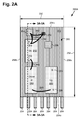
- Figure 2A shows an exemplary representation of such a packaging solution.
- FIG. 2A shows a top view of power unit 200A, according to one exemplary implementation.
- Power unit 200A includes power module 270 situated on a substrate (not visible from the perspective of Figure 2A ).
- power module 270 includes control transistor 210 (Q 1 ), sync transistor 220 (Q 2 ), switch node 232, output inductor 234, output capacitor 236, driver IC 240, electrical connectors 260, and encapsulant material 280.
- FIG. 2A shows also shown in Figure 2A.
- perspective lines 3A-3A corresponding to the cross-sectional view of power unit 200A shown by Figure 3A and discussed below.
- encapsulant material 280 may be any suitable electrically insulating material used as overmolding or encapsulation in semiconductor packaging. It is further noted that although, in practice, encapsulant material 280 is formed over and covers control transistor 210, sync transistor 220, switch node 232, output inductor 234, output capacitor 236, driver IC 240, and electrical connectors 280, Figure 2A depicts those features as though “seen through” encapsulant material 280 for the purposes of conceptual clarity.
- the substrate on which power module 270 is situated has length 252 determined by first and second ends 254a and 254b of the substrate, as well as width 256 determined by first and second edges 258a and 258b of the substrate.
- the substrate length 252 is greater than the substrate width 256.
- the substrate on which power module 270 is situated is itself situated on conductive slats each having an extended end away from power module 270, and each being one of mounting contacts 204.
- Mounting contacts 204 are electrically coupled to power module 270 by electrical routing within the substrate.
- Mounting contacts 204 are configured to provide electrical connections between power module 270 and a mother board into which power unit 200A is plugged (mother board not shown in Figure 2A ).
- power unit 200A is configured for end-mounting on the mother board.
- Power unit 200A including power module 270 corresponds in general to power unit 100 including power module 170, in Figure 1 , and may share any of the characteristics attributed to that corresponding feature in the present application.
- Control transistor 210, sync transistor 220, switch node 232, output inductor 234, and output capacitor 236, in Figure 2A correspond respectively in general to control transistor 110, sync transistor 120, switch node 132, output inductor 134, and output capacitor 136, in Figure 1 , and may share any of the characteristics attributed to those corresponding features in the present application.
- Control transistor 210 in Figure 2A , is shown to include top side source 214 and top side gate 216 corresponding respectively to source 114 and gate 116 of control transistor 110, in Figure 1
- sync transistor 220 is shown to include top side source 224 and top side gate 226 corresponding respectively to source 124 and gate 126 of sync transistor 120.
- control transistor 210 is implemented as a vertical power FET having a bottom side drain opposite top side source 214 and top side gate 216 and corresponding to drain 112 of control transistor 110, in Figure 1
- exemplary sync transistor 220 is also implemented as a vertical power FET having a bottom side drain opposite top side source 224 and top side gate 226 and corresponding to drain 122 of sync transistor 120, in Figure 1 .
- power module 270 includes driver IC 240, as well as all of the features included in power stage 130 of Figure 1 .
- driver IC 240 it may be advantageous or desirable to omit driver IC 240 from power module 270.
- power unit 200A may be configured to package control transistor 210, sync transistor 220, and one or both of output inductor 234 and output capacitor 236, but to omit driver IC 240.
- Mounting contacts 204 may be implemented using any suitable electrically conductive material or materials, and are collectively configured to provide power module 270 with electrical connections to ground, V IN , and V OUT , shown in Figure 1 .
- mounting contacts 204 may be extended ends of conductive slats that are part of a lead frame.
- the bottom side drain of sync transistor 220 corresponding to drain 122, in Figure 1 may be electrically connected to top side source 214 of control transistor 210 at switch node 232 by electrical routing within the substrate on which power module 270 is situated, as well as by electrical connectors 260. It is further noted that although electrical connectors 260 are depicted as wire bond in Figure 2A , that representation is merely for the purposes of conceptual clarity.
- electrical connectors 260 may be implemented as conductive clips, ribbons, strips, or vias, such as through-substrate vias, or as conductive traces on a printed circuit board (PCB).
- control transistor 210 may be coupled to sync transistor 220 by an electronic connector selected from the group consisting of a clip, a ribbon, a strip, a through-substrate via, a trace of a PCB, and a wire bond.
- driver IC 240 may be coupled to one or both of control transistor 210 and sync transistor 220 by an electrical connector selected from the group consisting of a clip, a ribbon, a strip, a through-substrate via, a trace of a PCB, and a wire bond.
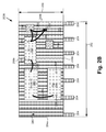
- Figure 2B shows a top view of power unit 200B for plugging into a mother board, according to another exemplary implementation. It is noted that all features in Figure 2B identified by reference numbers shown in and described by reference to Figure 2A , above, correspond respectively to those features and may share any of the characteristics attributed to those corresponding features in the present application.
- mounting contacts 204 of power unit 200B extend away from power module 270 at first edge 258a of the substrate on which power module 270 is situated. As described previously by reference to Figure 2A , mounting contacts 204 are electrically coupled to power module 270 by electrical routing within the substrate. Mounting contacts 204 are configured to provide electrical connections between power module 270 and a mother board into which power unit 200B is plugged (mother board not shown in Figure 2B ). Thus, power unit 200B is configured for edge-mounting on the mother board.
- FIG 3A shows a cross-sectional view of exemplary power unit 200A, in Figure 2A , according to one implementation, along perspective lines 3A-3A in Figure 2A .
- Power unit 300 includes substrate 302 having back surface 308b situated on conductive slats including conductive slat 390, and power module 370 situated on front surface 308a of substrate 302 opposite back surface 308b.
- Substrate 302 has length 352 determined by first and second ends 354a and 354b of substrate 302.
- power module 370 includes control transistor 310, driver IC 340 for driving control transistor 310, and output inductor 334, all situated on front surface 308a of substrate 302.
- power module 370 includes electrical connectors 360 and encapsulation material 380, and has exterior wall 372 situated adjacent mounting contacts 304 of power unit 300. Also shown in Figure 3A are drain 312, source 314, and gate 316 of control transistor 310.
- Power unit 300 including power module 370 corresponds in general to power unit 200A including power module 270, in Figure 2A , and may share any of the characteristics attributed to that corresponding feature in the present application. That is to say, substrate 302 having length 352 determined by first and second ends 354a and 354b of substrate 302 corresponds in general to the substrate having length 252 determined by first and second ends 254a and 254b, discussed by reference to Figure 2A , and may share any of the characteristics attributed to that corresponding feature in the present application.
- conductive slat 390 having an extended end away from power module 370 so as to be mounting contact 304 corresponds in general to the conductive slats serving as mounting contacts 204, discussed by reference to Figure 2A , and may share any of the characteristics attributed to those corresponding features, above.
- mounting contact 304 is electrically coupled to power module 370 by electrical routing in substrate 302.
- conductive slat 390 serving as mounting contact 304, as well as the conductive slats serving as mounting contacts 204, in Figures 2A and 2B may be part of a lead frame.
- conductive slat 390, in Figure 3A , as well as the conductive slats serving as mounting contacts 204, in Figures 2A and 2B may be formed of any suitable conductive material such as a metal or metal alloy, for example.
- substrate 302 may be a PCB configured as a daughter board for plugging into a mother board, for example.
- mounting contacts 304 can be electrically coupled to power module 370 by routing traces within the PCB of substrate 302.
- substrate 302 may include a molded interconnect system (MIS) as known in the art, and mounting contacts 304 can be electrically coupled to power module 370 by electrical connections produced in the MIS.
- MIS molded interconnect system
- power module 370 of power unit 300 also includes a sync transistor and output capacitor corresponding respectively to sync transistor 220 and output capacitor 236, in Figure 2A .
- exterior wall 372 of power module 370 adjacent mounting contacts 304 may be substantially perpendicular to front surface 308a of substrate 302.
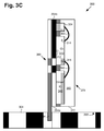
- Figure 3B shows a cross-sectional view of exemplary power unit 300 prior to being plugged into a mother board
- Figure shows power unit 300 plugged into the mother board. It is noted that all features in Figures 3B and 3C identified by reference numbers shown in and described by reference to Figure 3A , above, correspond respectively to those features and may share any of the characteristics attributed to those corresponding features in the present application.
- Figure 3B shows mother board 364 having major surface 368 including slot 366
- Figure 3C shows mounting contact 304 extending away from power module 370 at first end 354a of substrate 302 being plugged into slot 366. Consequently, mounting contacts 304 are placed into contact with electrical routing contained within mother board 364, which may be implemented as a PCB, so as to provide electrical connection between power module 370 and mother board 364.
- power unit 300 may be advantageously configured for end-mounting on mother board 364.
- end-mounting of power unit 300 on mother board 364 results in front surface 308a and back surface 308b of substrate 302 being substantially perpendicular to major surface 368 of mother board 364.
- power unit 200B in Figure 2B , may be analogously configured for edge-mounting on mother board 364.
- slot 366 would be configured to receive mounting contacts 204 extending away from power module 270 at first edge 258a of substrate 302.
- edge-mounting of power unit 200B on mother board 364 would also result in front surface 308a and back surface 308b of substrate 202/302 being substantially perpendicular to major surface 368 of mother board 364.
- the present application discloses a packaging solution in the form of a power unit with conductive slats providing mounting contacts for plugging into a mother board, that provides a highly compact design for packaging a voltage converter.
- the power unit with conductive slats disclosed in the present application may be configured for edge-mounting on a mother board, thereby substantially reducing the mother board surface area required to implement the voltage converter.
- such a power unit may be configured for end-mounting on the mother board, thereby advantageously further reducing use of mother board surface area.
Landscapes
- Engineering & Computer Science (AREA)
- Microelectronics & Electronic Packaging (AREA)
- Power Engineering (AREA)
- Dc-Dc Converters (AREA)
Abstract
Description
- The present application claims the benefit of and priority to a provisional application entitled "Module Card Structures," Serial No.
62/061,967 filed on October 9, 2014 - As used herein, "III-Nitride" or "III-N" refers to a compound semiconductor that includes nitrogen and at least one group III element such as aluminum (Al), gallium (Ga), indium (In), and boron (B), and including but not limited to any of its alloys, such as aluminum gallium nitride (AlxGa(1-x)N), indium gallium nitride (InyGa(1-y)N), aluminum indium gallium nitride (AlxInyGa(1-x-y)N), gallium arsenide phosphide nitride (GaAsaPbN(1-a-b)), aluminum indium gallium arsenide phosphide nitride (AlxInyGa(1-x-y)AsaPbN(1-a-b)), for example. III-N also refers generally to any polarity including but not limited to Ga-polar, N-polar, semi-polar, or non-polar crystal orientations. A III-N material may also include either the Wurtzitic, Zincblende, or mixed polytypes, and may include single-crystal, monocrystalline, polycrystalline, or amorphous structures. Gallium nitride or GaN, as used herein, refers to a III-N compound semiconductor wherein the group III element or elements include some or a substantial amount of gallium, but may also include other group III elements in addition to gallium. A III-N or a GaN transistor may also refer to a composite high-voltage enhancement mode transistor that is formed by connecting the III-N or the GaN transistor in cascode with a lower voltage group IV transistor.
- In addition, as used herein, the phrase "group IV" refers to a semiconductor that includes at least one group IV element such as silicon (Si), germanium (Ge), and carbon (C), and may also include compound semiconductors such as silicon germanium (SiGe) and silicon carbide (SiC), for example. Group IV also refers to semiconductor materials which include more than one layer of group IV elements, or doping of group IV elements to produce strained group IV materials, and may also include group IV based composite substrates such as silicon on insulator (SOI), separation by implantation of oxygen (SIMOX) process substrates, and silicon on sapphire (SOS), for example.
- Voltage converters are used in a variety of electronic circuits and systems. Many integrated circuit (IC) applications, for instance, require conversion of a direct current (DC) input to a lower, or higher, DC output. For example, a buck converter may be implemented to convert a higher voltage DC input to a lower voltage DC output for use in low voltage applications in which relatively large output currents are required.
- The output of a voltage converter is typically provided by a power stage including a high side control transistor and a low side synchronous (sync) transistor, and may utilize relatively large passive devices, such as an output inductor and output capacitor. In addition, voltage converter circuitry typically includes a driver IC designed to drive the control and sync transistors of the power stage. Consequently, packaging solutions for mounting a voltage converter on a mother board typically require mother board surface area sufficient to accommodate a side-by-side layout including not only the control and sync transistors of the voltage converter power stage, but the output inductor, the output capacitor, and the driver IC for the power stage as well.
- The present disclosure is directed to a power unit with conductive slats, substantially as shown in and/or described in connection with at least one of the figures, and as set forth in the claims.
-
-
Figure 1 shows a diagram of a power unit, according to one exemplary implementation. -
Figure 2A shows a top view of a power unit with conductive slats providing mounting contacts for plugging into a mother board, according to one exemplary implementation. -
Figure 2B shows a top view of a power unit with conductive slats providing mounting contacts for plugging into a mother board, according to another exemplary implementation. -
Figure 3A shows a cross-sectional view of the exemplary power unit shown inFigure 2A . -
Figure 3B shows a cross-sectional view of the exemplary power unit shown inFigure 2A prior to being plugged into a mother board. -
Figure 3C shows a cross-sectional view of the exemplary power unit shown inFigure 2A plugged into the mother board shown inFigure 3B . - The following description contains specific information pertaining to implementations in the present disclosure. One skilled in the art will recognize that the present disclosure may be implemented in a manner different from that specifically discussed herein. The drawings in the present application and their accompanying detailed description are directed to merely exemplary implementations. Unless noted otherwise, like or corresponding elements among the figures may be indicated by like or corresponding reference numerals. Moreover, the drawings and illustrations in the present application are generally not to scale, and are not intended to correspond to actual relative dimensions.
- As stated above, voltage converters are used in a variety of electronic circuits and systems. For instance, and as noted above, integrated circuit (IC) applications may require conversion of a direct current (DC) input to a lower, or higher, DC output. As a specific example, a buck converter may be implemented to convert a higher voltage DC input to a lower voltage DC output for use in low voltage applications in which relatively large output currents are required.
-
Figure 1 shows a diagram of a power unit including a voltage converter, according to one exemplary implementation.Power unit 100 includespower module 170 containing a voltage converter provided bypower stage 130 and driver IC 140 fordriving power stage 130. According to the exemplary implementation shown inFigure 1 ,power stage 130 includes control transistor 110 (Q1), synchronous (sync) transistor 120 (Q2),output inductor 134, andoutput capacitor 136. As shown inFigure 1 ,power module 170 ofpower unit 100 is configured to receive an input voltage VIN, and to provide a converted voltage, e.g., a rectified and/or stepped down voltage, as VOUT. -
Power stage 130 may be implemented using two power transistors in the form of metal-oxide-semiconductor field-effect transistors (MOSFETs) configured as a half bridge, for example. That is to say,power stage 130 may include high side orcontrol transistor 110 havingdrain 112,source 114, andgate 116, as well as low side orsync transistor 120 havingdrain 122, source 124, andgate 126.Control transistor 110 is coupled withsync transistor 120 atswitch node 132, which, in turn, is coupled tooutput inductor 134. Respective control andsync transistors Power module 170 may be advantageously utilized as a voltage converter, for example a buck converter, in a variety of automotive, industrial, appliance, and lighting applications. - It is noted that in the interests of ease and conciseness of description, the present inventive principles will in some instances be described by reference to specific implementations of a buck converter including one or more silicon based power FETs. However, it is emphasized that such implementations are merely exemplary, and the inventive principles disclosed herein are broadly applicable to a wide range of applications, including buck and boost converters, implemented using other group IV material based, or group III-V semiconductor based, power transistors. By way of example,
control transistor 110 andsync transistor 120 may be implemented as III-Nitride power transistors in the form of heterostructure FETs (HFETs) such as gallium nitride (GaN) or other III-Nitride high electron mobility transistors (HEMTs). - As shown in
Figure 1 , the voltage converter packaged bypower unit 100 utilizespower stage 130 includingcontrol transistor 110,sync transistor 120,output inductor 134, andoutput capacitor 136 to provide output voltage VOUT. In addition, the voltage converter packaged bypower unit 100 includesdriver IC 140. As a result, conventional packaging solutions for mounting such a voltage converter on a mother board would typically require mother board surface area sufficient to accommodate a side-by-side layout including not onlycontrol transistor 110 andsync transistor 120, butoutput inductor 134,output capacitor 136, anddriver IC 140 as well. - The present application discloses a packaging solution in the form of a power unit with conductive slats providing mounting contacts for plugging into a mother board, that provides a highly compact design for
packaging power stage 130, alone, or in combination with driver IC 140, aspower module 170. As discussed below,power unit 100 may be configured for edge-mounting on a mother board, thereby substantially reducing the mother board surface area required to implement the voltage converter. Alternatively, and as further discussed below,power unit 100 may be configured for end-mounting on the mother board, thereby advantageously further reducing use of mother board surface area.Figure 2A shows an exemplary representation of such a packaging solution. -
Figure 2A shows a top view ofpower unit 200A, according to one exemplary implementation.Power unit 200A includespower module 270 situated on a substrate (not visible from the perspective ofFigure 2A ). According to the exemplary implementation shown inFigure 2A ,power module 270 includes control transistor 210 (Q1), sync transistor 220 (Q2),switch node 232,output inductor 234,output capacitor 236,driver IC 240,electrical connectors 260, andencapsulant material 280. Also shown inFigure 2A areperspective lines 3A-3A corresponding to the cross-sectional view ofpower unit 200A shown byFigure 3A and discussed below. - It is noted that
encapsulant material 280 may be any suitable electrically insulating material used as overmolding or encapsulation in semiconductor packaging. It is further noted that although, in practice,encapsulant material 280 is formed over and coverscontrol transistor 210,sync transistor 220,switch node 232,output inductor 234,output capacitor 236,driver IC 240, andelectrical connectors 280,Figure 2A depicts those features as though "seen through"encapsulant material 280 for the purposes of conceptual clarity. - The substrate on which
power module 270 is situated haslength 252 determined by first andsecond ends width 256 determined by first andsecond edges substrate length 252 is greater than thesubstrate width 256. - The substrate on which
power module 270 is situated, is itself situated on conductive slats each having an extended end away frompower module 270, and each being one ofmounting contacts 204.Mounting contacts 204 are electrically coupled topower module 270 by electrical routing within the substrate. Mountingcontacts 204 are configured to provide electrical connections betweenpower module 270 and a mother board into whichpower unit 200A is plugged (mother board not shown inFigure 2A ). Thus,power unit 200A is configured for end-mounting on the mother board. -
Power unit 200A includingpower module 270 corresponds in general topower unit 100 includingpower module 170, inFigure 1 , and may share any of the characteristics attributed to that corresponding feature in the present application.Control transistor 210,sync transistor 220,switch node 232,output inductor 234, andoutput capacitor 236, inFigure 2A correspond respectively in general to controltransistor 110,sync transistor 120,switch node 132,output inductor 134, andoutput capacitor 136, inFigure 1 , and may share any of the characteristics attributed to those corresponding features in the present application. -
Control transistor 210, inFigure 2A , is shown to includetop side source 214 andtop side gate 216 corresponding respectively to source 114 andgate 116 ofcontrol transistor 110, inFigure 1 , whilesync transistor 220 is shown to includetop side source 224 andtop side gate 226 corresponding respectively to source 124 andgate 126 ofsync transistor 120. Although not visible in the perspective shown inFigure 2A , it is to be understood that, according to the present exemplary implementation,control transistor 210 is implemented as a vertical power FET having a bottom side drain oppositetop side source 214 andtop side gate 216 and corresponding to drain 112 ofcontrol transistor 110, inFigure 1 . Moreover,exemplary sync transistor 220 is also implemented as a vertical power FET having a bottom side drain oppositetop side source 224 andtop side gate 226 and corresponding to drain 122 ofsync transistor 120, inFigure 1 . - According to the exemplary implementation shown in
Figure 2A ,power module 270 includesdriver IC 240, as well as all of the features included inpower stage 130 ofFigure 1 . However, in some implementations, it may be advantageous or desirable to omitdriver IC 240 frompower module 270. In those implementations,power unit 200A may be configured to packagecontrol transistor 210,sync transistor 220, and one or both ofoutput inductor 234 andoutput capacitor 236, but to omitdriver IC 240. - Mounting
contacts 204 may be implemented using any suitable electrically conductive material or materials, and are collectively configured to providepower module 270 with electrical connections to ground, VIN, and VOUT, shown inFigure 1 . For example, in some implementations, mountingcontacts 204 may be extended ends of conductive slats that are part of a lead frame. - With respect to electrical connections among the features contained by
power module 270, it is noted that the bottom side drain ofsync transistor 220 corresponding to drain 122, inFigure 1 , may be electrically connected totop side source 214 ofcontrol transistor 210 atswitch node 232 by electrical routing within the substrate on whichpower module 270 is situated, as well as byelectrical connectors 260. It is further noted that althoughelectrical connectors 260 are depicted as wire bond inFigure 2A , that representation is merely for the purposes of conceptual clarity. - More generally,
electrical connectors 260 may be implemented as conductive clips, ribbons, strips, or vias, such as through-substrate vias, or as conductive traces on a printed circuit board (PCB). In other words,control transistor 210 may be coupled tosync transistor 220 by an electronic connector selected from the group consisting of a clip, a ribbon, a strip, a through-substrate via, a trace of a PCB, and a wire bond. In addition,driver IC 240 may be coupled to one or both ofcontrol transistor 210 andsync transistor 220 by an electrical connector selected from the group consisting of a clip, a ribbon, a strip, a through-substrate via, a trace of a PCB, and a wire bond. - Moving to
Figure 2B, Figure 2B shows a top view ofpower unit 200B for plugging into a mother board, according to another exemplary implementation. It is noted that all features inFigure 2B identified by reference numbers shown in and described by reference toFigure 2A , above, correspond respectively to those features and may share any of the characteristics attributed to those corresponding features in the present application. - In contrast to
power unit 200A, inFigure 2A , however, mountingcontacts 204 ofpower unit 200B extend away frompower module 270 atfirst edge 258a of the substrate on whichpower module 270 is situated. As described previously by reference toFigure 2A , mountingcontacts 204 are electrically coupled topower module 270 by electrical routing within the substrate. Mountingcontacts 204 are configured to provide electrical connections betweenpower module 270 and a mother board into whichpower unit 200B is plugged (mother board not shown inFigure 2B ). Thus,power unit 200B is configured for edge-mounting on the mother board. - Referring to
Figure 3A, Figure 3A shows a cross-sectional view ofexemplary power unit 200A, inFigure 2A , according to one implementation, alongperspective lines 3A-3A inFigure 2A .Power unit 300 includessubstrate 302 having backsurface 308b situated on conductive slats includingconductive slat 390, andpower module 370 situated onfront surface 308a ofsubstrate 302opposite back surface 308b.Substrate 302 haslength 352 determined by first andsecond ends substrate 302. As shown inFigure 3A ,power module 370 includescontrol transistor 310,driver IC 340 for drivingcontrol transistor 310, andoutput inductor 334, all situated onfront surface 308a ofsubstrate 302. As further shown inFigure 3A ,power module 370 includeselectrical connectors 360 andencapsulation material 380, and hasexterior wall 372 situated adjacent mountingcontacts 304 ofpower unit 300. Also shown inFigure 3A aredrain 312,source 314, andgate 316 ofcontrol transistor 310. -
Power unit 300 includingpower module 370 corresponds in general topower unit 200A includingpower module 270, inFigure 2A , and may share any of the characteristics attributed to that corresponding feature in the present application. That is to say,substrate 302 havinglength 352 determined by first andsecond ends substrate 302 corresponds in general to thesubstrate having length 252 determined by first andsecond ends Figure 2A , and may share any of the characteristics attributed to that corresponding feature in the present application. In addition,conductive slat 390 having an extended end away frompower module 370 so as to be mountingcontact 304 corresponds in general to the conductive slats serving as mountingcontacts 204, discussed by reference toFigure 2A , and may share any of the characteristics attributed to those corresponding features, above. Thus, mountingcontact 304 is electrically coupled topower module 370 by electrical routing insubstrate 302. - As noted above,
conductive slat 390 serving as mountingcontact 304, as well as the conductive slats serving as mountingcontacts 204, inFigures 2A and2B , may be part of a lead frame. Alternatively,conductive slat 390, inFigure 3A , as well as the conductive slats serving as mountingcontacts 204, inFigures 2A and2B , may be formed of any suitable conductive material such as a metal or metal alloy, for example. - In one implementation,
substrate 302 may be a PCB configured as a daughter board for plugging into a mother board, for example. In that implementation, mountingcontacts 304 can be electrically coupled topower module 370 by routing traces within the PCB ofsubstrate 302. In another implementation, for example,substrate 302 may include a molded interconnect system (MIS) as known in the art, and mountingcontacts 304 can be electrically coupled topower module 370 by electrical connections produced in the MIS. - It is noted that although not visible from the perspective shown by
Figure 3A , due to being obscured bycontrol transistor 310,driver IC 340, andencapsulation material 380,power module 370 ofpower unit 300 also includes a sync transistor and output capacitor corresponding respectively to synctransistor 220 andoutput capacitor 236, inFigure 2A . In addition to the features previously attributed topower unit 100/200A/ 200B/300, it is noted thatexterior wall 372 ofpower module 370 adjacent mountingcontacts 304 may be substantially perpendicular tofront surface 308a ofsubstrate 302. - Continuing to
Figures 3B and3C ,Figure 3B shows a cross-sectional view ofexemplary power unit 300 prior to being plugged into a mother board, while Figure showspower unit 300 plugged into the mother board. It is noted that all features inFigures 3B and3C identified by reference numbers shown in and described by reference toFigure 3A , above, correspond respectively to those features and may share any of the characteristics attributed to those corresponding features in the present application. - In addition to
power unit 300,Figure 3B showsmother board 364 havingmajor surface 368 includingslot 366, whileFigure 3C shows mountingcontact 304 extending away frompower module 370 atfirst end 354a ofsubstrate 302 being plugged intoslot 366. Consequently, mountingcontacts 304 are placed into contact with electrical routing contained withinmother board 364, which may be implemented as a PCB, so as to provide electrical connection betweenpower module 370 andmother board 364. - Thus, according to the implementation shown by
Figures 3A ,3B , and3C power unit 300 may be advantageously configured for end-mounting onmother board 364. According to the implementation shown inFigures 3A ,3B , and3C , end-mounting ofpower unit 300 onmother board 364 results infront surface 308a and backsurface 308b ofsubstrate 302 being substantially perpendicular tomajor surface 368 ofmother board 364. - It is noted that
power unit 200B, inFigure 2B , may be analogously configured for edge-mounting onmother board 364. In that implementation, however, slot 366 would be configured to receive mountingcontacts 204 extending away frompower module 270 atfirst edge 258a ofsubstrate 302. It is noted that edge-mounting ofpower unit 200B onmother board 364 would also result infront surface 308a and backsurface 308b of substrate 202/302 being substantially perpendicular tomajor surface 368 ofmother board 364. - Thus, the present application discloses a packaging solution in the form of a power unit with conductive slats providing mounting contacts for plugging into a mother board, that provides a highly compact design for packaging a voltage converter. The power unit with conductive slats disclosed in the present application may be configured for edge-mounting on a mother board, thereby substantially reducing the mother board surface area required to implement the voltage converter. Alternatively, such a power unit may be configured for end-mounting on the mother board, thereby advantageously further reducing use of mother board surface area.
- From the above description it is manifest that various techniques can be used for implementing the concepts described in the present application without departing from the scope of those concepts. Moreover, while the concepts have been described with specific reference to certain implementations, a person of ordinary skill in the art would recognize that changes can be made in form and detail without departing from the scope of those concepts. As such, the described implementations are to be considered in all respects as illustrative and not restrictive. It should also be understood that the present application is not limited to the particular implementations described herein, but many rearrangements, modifications, and substitutions are possible without departing from the scope of the present disclosure.
Claims (15)
- A power unit for plugging into a mother board, said power unit comprising:a power module situated on a substrate;said substrate being situated on a plurality of conductive slats each having an extended end away from said power module;each said extended end of said plurality of conductive slats being a mounting contact;each said mounting contact being electrically coupled to said power module by an electrical routing in said substrate;each said mounting contact configured to provide electrical connection between said power module and said mother board.
- The power unit of claim 1, wherein said substrate comprises a printed circuit board (PCB) configured as a daughter board.
- The power unit of claim 1, wherein said substrate comprises a molded interconnect system (MIS).
- The power unit of claim 1, wherein each said mounting contact is at an end of said substrate for end-mounting on said mother board.
- The power unit of claim 1, wherein each said mounting contact is at an edge of said substrate for edge-mounting on said mother board.
- The power unit of claim 1, wherein said plurality of conductive slats are part of a lead frame.
- A power unit for plugging into a mother board, said power unit comprising:a power module including a control transistor and a sync transistor of a power stage situated on a substrate;said substrate being situated on a plurality of conductive slats each having an extended end away from said power module;each said extended end of said plurality of conductive slats being a mounting contact;each said mounting contact being electrically coupled to said power module by an electrical routing in said substrate;each said mounting contact configured to provide electrical connection between said power module and said mother board.
- The power unit of claim 7, wherein said substrate comprises a printed circuit board (PCB) configured as a daughter board.
- The power unit of claim 7, wherein said substrate comprises a molded interconnect system (MIS).
- The power unit of claim 7, wherein each said mounting contact is at an end of said substrate for end-mounting on said mother board.
- The power unit of claim 7, wherein each said mounting contact is at an edge of said substrate for edge-mounting on said mother board.
- The power unit of claim 7, wherein said plurality of conductive slats are part of a lead frame.
- The power unit of claim 7, wherein said control transistor is coupled to said sync transistor by an electrical connector selected from the group consisting of a clip, a ribbon, a strip, a through-substrate via, a trace of a printed circuit board, and a wire bond.
- The power unit of claim 7, wherein said power module comprises a driver integrated circuit.
- The power unit of claim 14, wherein said driver integrated circuit is coupled to at least one of said control transistor and said sync transistor by an electrical connector selected from the group consisting of a clip, a ribbon, a strip, a through-substrate via, a trace of a printed circuit board, and a wire bond.
Applications Claiming Priority (2)
| Application Number | Priority Date | Filing Date | Title |
|---|---|---|---|
| US201462061967P | 2014-10-09 | 2014-10-09 | |
| US14/857,536 US20160105984A1 (en) | 2014-10-09 | 2015-09-17 | Power Unit with Conductive Slats |
Publications (1)
| Publication Number | Publication Date |
|---|---|
| EP3007343A1 true EP3007343A1 (en) | 2016-04-13 |
Family
ID=54256513
Family Applications (1)
| Application Number | Title | Priority Date | Filing Date |
|---|---|---|---|
| EP15186377.6A Withdrawn EP3007343A1 (en) | 2014-10-09 | 2015-09-23 | Power unit with conductive slats |
Country Status (2)
| Country | Link |
|---|---|
| US (1) | US20160105984A1 (en) |
| EP (1) | EP3007343A1 (en) |
Cited By (1)
| Publication number | Priority date | Publication date | Assignee | Title |
|---|---|---|---|---|
| EP4040045A1 (en) * | 2021-02-03 | 2022-08-10 | Self Electronics Co., Ltd. | Led power supply |
Families Citing this family (2)
| Publication number | Priority date | Publication date | Assignee | Title |
|---|---|---|---|---|
| CN109548280A (en) * | 2018-11-09 | 2019-03-29 | 天津航空机电有限公司 | A kind of card insert type power output circuit board being individually replaced |
| IT202300017841A1 (en) | 2023-08-30 | 2025-03-02 | St Microelectronics Int Nv | PROCEDURE FOR MANUFACTURING SEMICONDUCTOR DEVICES AND CORRESPONDING SEMICONDUCTOR DEVICE |
Citations (5)
| Publication number | Priority date | Publication date | Assignee | Title |
|---|---|---|---|---|
| EP0766504A2 (en) * | 1995-09-29 | 1997-04-02 | Allen-Bradley Company, Inc. | A wireless circuit board system for a motor controller |
| US5670749A (en) * | 1995-09-29 | 1997-09-23 | Allen-Bradley Company, Inc. | Multilayer circuit board having a window exposing an enhanced conductive layer for use as an insulated mounting area |
| US5907475A (en) * | 1996-04-16 | 1999-05-25 | Allen-Bradley Company, Llc | Circuit board system having a mounted board and a plurality of mounting boards |
| US20080012099A1 (en) * | 2006-07-11 | 2008-01-17 | Shing Yeh | Electronic assembly and manufacturing method having a reduced need for wire bonds |
| US20090108821A1 (en) * | 2007-03-07 | 2009-04-30 | Martin Standing | Multi-phase voltage regulation module |
Family Cites Families (3)
| Publication number | Priority date | Publication date | Assignee | Title |
|---|---|---|---|---|
| JP2001024312A (en) * | 1999-07-13 | 2001-01-26 | Taiyo Yuden Co Ltd | Electronic device manufacturing method, electronic device, and resin filling method |
| US7254036B2 (en) * | 2004-04-09 | 2007-08-07 | Netlist, Inc. | High density memory module using stacked printed circuit boards |
| JP5588419B2 (en) * | 2011-10-26 | 2014-09-10 | 株式会社東芝 | package |
-
2015
- 2015-09-17 US US14/857,536 patent/US20160105984A1/en not_active Abandoned
- 2015-09-23 EP EP15186377.6A patent/EP3007343A1/en not_active Withdrawn
Patent Citations (5)
| Publication number | Priority date | Publication date | Assignee | Title |
|---|---|---|---|---|
| EP0766504A2 (en) * | 1995-09-29 | 1997-04-02 | Allen-Bradley Company, Inc. | A wireless circuit board system for a motor controller |
| US5670749A (en) * | 1995-09-29 | 1997-09-23 | Allen-Bradley Company, Inc. | Multilayer circuit board having a window exposing an enhanced conductive layer for use as an insulated mounting area |
| US5907475A (en) * | 1996-04-16 | 1999-05-25 | Allen-Bradley Company, Llc | Circuit board system having a mounted board and a plurality of mounting boards |
| US20080012099A1 (en) * | 2006-07-11 | 2008-01-17 | Shing Yeh | Electronic assembly and manufacturing method having a reduced need for wire bonds |
| US20090108821A1 (en) * | 2007-03-07 | 2009-04-30 | Martin Standing | Multi-phase voltage regulation module |
Non-Patent Citations (1)
| Title |
|---|
| "Buck/Boost Converter PICtail(TM) Plus Daughter Board User's Guide", 25 March 2014 (2014-03-25), pages 1 - 56, XP055252553, Retrieved from the Internet <URL:http://ww1.microchip.com/downloads/en/DeviceDoc/70000336c.pdf> [retrieved on 20160223] * |
Cited By (1)
| Publication number | Priority date | Publication date | Assignee | Title |
|---|---|---|---|---|
| EP4040045A1 (en) * | 2021-02-03 | 2022-08-10 | Self Electronics Co., Ltd. | Led power supply |
Also Published As
| Publication number | Publication date |
|---|---|
| US20160105984A1 (en) | 2016-04-14 |
Similar Documents
| Publication | Publication Date | Title |
|---|---|---|
| EP2511953B1 (en) | Stacked composite device including a group III-V transistor and a group IV lateral transistor | |
| US10083884B2 (en) | Compact high-voltage semiconductor package | |
| US9041067B2 (en) | Integrated half-bridge circuit with low side and high side composite switches | |
| EP2521176B1 (en) | High voltage cascoded III-nitride rectifier package comprising conductive clips between electrodes of components and the surface of a package support member | |
| US10332825B2 (en) | Semiconductor package including flip chip mounted IC and vertically integrated inductor | |
| US9515014B2 (en) | Power converter package with integrated output inductor | |
| EP3007342A1 (en) | Insertable power unit with mounting contacts for plugging into a mother board | |
| US9202811B2 (en) | Cascode circuit integration of group III-N and group IV devices | |
| EP2511952A1 (en) | Stacked composite device including a group III-V transistor and a group IV vertical transistor | |
| US9831159B2 (en) | Semiconductor package with embedded output inductor | |
| US11387179B2 (en) | IC package with half-bridge power module | |
| JP2014054173A (en) | Integrated group iii-v power stage | |
| US9496168B2 (en) | Semiconductor package with via-coupled power transistors | |
| US20170117213A1 (en) | Semiconductor package with integrated die paddles for power stage | |
| US9099452B2 (en) | Semiconductor package with low profile switch node integrated heat spreader | |
| EP2521172A1 (en) | High voltage cascoded III-nitride rectifier package with etched leadframe | |
| US20160105984A1 (en) | Power Unit with Conductive Slats | |
| US20240421139A1 (en) | Module assembly of multiple semiconductor devices with insulating substrates | |
| US9768099B1 (en) | IC package with integrated inductor | |
| EP3168871B1 (en) | Semiconductor device and a method of making a semiconductor device |
Legal Events
| Date | Code | Title | Description |
|---|---|---|---|
| PUAI | Public reference made under article 153(3) epc to a published international application that has entered the european phase |
Free format text: ORIGINAL CODE: 0009012 |
|
| AK | Designated contracting states |
Kind code of ref document: A1 Designated state(s): AL AT BE BG CH CY CZ DE DK EE ES FI FR GB GR HR HU IE IS IT LI LT LU LV MC MK MT NL NO PL PT RO RS SE SI SK SM TR |
|
| AX | Request for extension of the european patent |
Extension state: BA ME |
|
| 17P | Request for examination filed |
Effective date: 20161012 |
|
| RBV | Designated contracting states (corrected) |
Designated state(s): AL AT BE BG CH CY CZ DE DK EE ES FI FR GB GR HR HU IE IS IT LI LT LU LV MC MK MT NL NO PL PT RO RS SE SI SK SM TR |
|
| 17Q | First examination report despatched |
Effective date: 20170608 |
|
| RAP1 | Party data changed (applicant data changed or rights of an application transferred) |
Owner name: INFINEON TECHNOLOGIES AMERICAS CORP. |
|
| STAA | Information on the status of an ep patent application or granted ep patent |
Free format text: STATUS: THE APPLICATION IS DEEMED TO BE WITHDRAWN |
|
| 18D | Application deemed to be withdrawn |
Effective date: 20190726 |