EP3007223A1 - Power converter package with integrated output inductor - Google Patents
Power converter package with integrated output inductor Download PDFInfo
- Publication number
- EP3007223A1 EP3007223A1 EP15185987.3A EP15185987A EP3007223A1 EP 3007223 A1 EP3007223 A1 EP 3007223A1 EP 15185987 A EP15185987 A EP 15185987A EP 3007223 A1 EP3007223 A1 EP 3007223A1
- Authority
- EP
- European Patent Office
- Prior art keywords
- conductive carrier
- patterned conductive
- sync
- fet
- control
- Prior art date
- Legal status (The legal status is an assumption and is not a legal conclusion. Google has not performed a legal analysis and makes no representation as to the accuracy of the status listed.)
- Granted
Links
Images




Classifications
-
- H—ELECTRICITY
- H02—GENERATION; CONVERSION OR DISTRIBUTION OF ELECTRIC POWER
- H02M—APPARATUS FOR CONVERSION BETWEEN AC AND AC, BETWEEN AC AND DC, OR BETWEEN DC AND DC, AND FOR USE WITH MAINS OR SIMILAR POWER SUPPLY SYSTEMS; CONVERSION OF DC OR AC INPUT POWER INTO SURGE OUTPUT POWER; CONTROL OR REGULATION THEREOF
- H02M7/00—Conversion of AC power input into DC power output; Conversion of DC power input into AC power output
- H02M7/003—Constructional details, e.g. physical layout, assembly, wiring or busbar connections
-
- H—ELECTRICITY
- H02—GENERATION; CONVERSION OR DISTRIBUTION OF ELECTRIC POWER
- H02M—APPARATUS FOR CONVERSION BETWEEN AC AND AC, BETWEEN AC AND DC, OR BETWEEN DC AND DC, AND FOR USE WITH MAINS OR SIMILAR POWER SUPPLY SYSTEMS; CONVERSION OF DC OR AC INPUT POWER INTO SURGE OUTPUT POWER; CONTROL OR REGULATION THEREOF
- H02M3/00—Conversion of DC power input into DC power output
- H02M3/02—Conversion of DC power input into DC power output without intermediate conversion into AC
- H02M3/04—Conversion of DC power input into DC power output without intermediate conversion into AC by static converters
- H02M3/10—Conversion of DC power input into DC power output without intermediate conversion into AC by static converters using discharge tubes with control electrode or semiconductor devices with control electrode
- H02M3/145—Conversion of DC power input into DC power output without intermediate conversion into AC by static converters using discharge tubes with control electrode or semiconductor devices with control electrode using devices of a triode or transistor type requiring continuous application of a control signal
- H02M3/155—Conversion of DC power input into DC power output without intermediate conversion into AC by static converters using discharge tubes with control electrode or semiconductor devices with control electrode using devices of a triode or transistor type requiring continuous application of a control signal using semiconductor devices only
- H02M3/156—Conversion of DC power input into DC power output without intermediate conversion into AC by static converters using discharge tubes with control electrode or semiconductor devices with control electrode using devices of a triode or transistor type requiring continuous application of a control signal using semiconductor devices only with automatic control of output voltage or current, e.g. switching regulators
- H02M3/158—Conversion of DC power input into DC power output without intermediate conversion into AC by static converters using discharge tubes with control electrode or semiconductor devices with control electrode using devices of a triode or transistor type requiring continuous application of a control signal using semiconductor devices only with automatic control of output voltage or current, e.g. switching regulators including plural semiconductor devices as final control devices for a single load
-
- H—ELECTRICITY
- H02—GENERATION; CONVERSION OR DISTRIBUTION OF ELECTRIC POWER
- H02M—APPARATUS FOR CONVERSION BETWEEN AC AND AC, BETWEEN AC AND DC, OR BETWEEN DC AND DC, AND FOR USE WITH MAINS OR SIMILAR POWER SUPPLY SYSTEMS; CONVERSION OF DC OR AC INPUT POWER INTO SURGE OUTPUT POWER; CONTROL OR REGULATION THEREOF
- H02M3/00—Conversion of DC power input into DC power output
- H02M3/02—Conversion of DC power input into DC power output without intermediate conversion into AC
- H02M3/04—Conversion of DC power input into DC power output without intermediate conversion into AC by static converters
- H02M3/10—Conversion of DC power input into DC power output without intermediate conversion into AC by static converters using discharge tubes with control electrode or semiconductor devices with control electrode
- H02M3/145—Conversion of DC power input into DC power output without intermediate conversion into AC by static converters using discharge tubes with control electrode or semiconductor devices with control electrode using devices of a triode or transistor type requiring continuous application of a control signal
- H02M3/155—Conversion of DC power input into DC power output without intermediate conversion into AC by static converters using discharge tubes with control electrode or semiconductor devices with control electrode using devices of a triode or transistor type requiring continuous application of a control signal using semiconductor devices only
- H02M3/156—Conversion of DC power input into DC power output without intermediate conversion into AC by static converters using discharge tubes with control electrode or semiconductor devices with control electrode using devices of a triode or transistor type requiring continuous application of a control signal using semiconductor devices only with automatic control of output voltage or current, e.g. switching regulators
- H02M3/158—Conversion of DC power input into DC power output without intermediate conversion into AC by static converters using discharge tubes with control electrode or semiconductor devices with control electrode using devices of a triode or transistor type requiring continuous application of a control signal using semiconductor devices only with automatic control of output voltage or current, e.g. switching regulators including plural semiconductor devices as final control devices for a single load
- H02M3/1588—Conversion of DC power input into DC power output without intermediate conversion into AC by static converters using discharge tubes with control electrode or semiconductor devices with control electrode using devices of a triode or transistor type requiring continuous application of a control signal using semiconductor devices only with automatic control of output voltage or current, e.g. switching regulators including plural semiconductor devices as final control devices for a single load comprising at least one synchronous rectifier element
-
- H—ELECTRICITY
- H02—GENERATION; CONVERSION OR DISTRIBUTION OF ELECTRIC POWER
- H02M—APPARATUS FOR CONVERSION BETWEEN AC AND AC, BETWEEN AC AND DC, OR BETWEEN DC AND DC, AND FOR USE WITH MAINS OR SIMILAR POWER SUPPLY SYSTEMS; CONVERSION OF DC OR AC INPUT POWER INTO SURGE OUTPUT POWER; CONTROL OR REGULATION THEREOF
- H02M7/00—Conversion of AC power input into DC power output; Conversion of DC power input into AC power output
- H02M7/02—Conversion of AC power input into DC power output without possibility of reversal
- H02M7/04—Conversion of AC power input into DC power output without possibility of reversal by static converters
- H02M7/12—Conversion of AC power input into DC power output without possibility of reversal by static converters using discharge tubes with control electrode or semiconductor devices with control electrode
- H02M7/21—Conversion of AC power input into DC power output without possibility of reversal by static converters using discharge tubes with control electrode or semiconductor devices with control electrode using devices of a triode or transistor type requiring continuous application of a control signal
- H02M7/217—Conversion of AC power input into DC power output without possibility of reversal by static converters using discharge tubes with control electrode or semiconductor devices with control electrode using devices of a triode or transistor type requiring continuous application of a control signal using semiconductor devices only
-
- H—ELECTRICITY
- H10—SEMICONDUCTOR DEVICES; ELECTRIC SOLID-STATE DEVICES NOT OTHERWISE PROVIDED FOR
- H10D—INORGANIC ELECTRIC SEMICONDUCTOR DEVICES
- H10D1/00—Resistors, capacitors or inductors
- H10D1/20—Inductors
-
- H—ELECTRICITY
- H10—SEMICONDUCTOR DEVICES; ELECTRIC SOLID-STATE DEVICES NOT OTHERWISE PROVIDED FOR
- H10D—INORGANIC ELECTRIC SEMICONDUCTOR DEVICES
- H10D30/00—Field-effect transistors [FET]
- H10D30/40—FETs having zero-dimensional [0D], one-dimensional [1D] or two-dimensional [2D] charge carrier gas channels
- H10D30/47—FETs having zero-dimensional [0D], one-dimensional [1D] or two-dimensional [2D] charge carrier gas channels having two-dimensional [2D] charge carrier gas channels, e.g. nanoribbon FETs or high electron mobility transistors [HEMT]
- H10D30/471—High electron mobility transistors [HEMT] or high hole mobility transistors [HHMT]
- H10D30/475—High electron mobility transistors [HEMT] or high hole mobility transistors [HHMT] having wider bandgap layer formed on top of lower bandgap active layer, e.g. undoped barrier HEMTs such as i-AlGaN/GaN HEMTs
- H10D30/4755—High electron mobility transistors [HEMT] or high hole mobility transistors [HHMT] having wider bandgap layer formed on top of lower bandgap active layer, e.g. undoped barrier HEMTs such as i-AlGaN/GaN HEMTs having wide bandgap charge-carrier supplying layers, e.g. modulation doped HEMTs such as n-AlGaAs/GaAs HEMTs
-
- H—ELECTRICITY
- H10—SEMICONDUCTOR DEVICES; ELECTRIC SOLID-STATE DEVICES NOT OTHERWISE PROVIDED FOR
- H10D—INORGANIC ELECTRIC SEMICONDUCTOR DEVICES
- H10D30/00—Field-effect transistors [FET]
- H10D30/60—Insulated-gate field-effect transistors [IGFET]
- H10D30/64—Double-diffused metal-oxide semiconductor [DMOS] FETs
-
- H—ELECTRICITY
- H10—SEMICONDUCTOR DEVICES; ELECTRIC SOLID-STATE DEVICES NOT OTHERWISE PROVIDED FOR
- H10D—INORGANIC ELECTRIC SEMICONDUCTOR DEVICES
- H10D62/00—Semiconductor bodies, or regions thereof, of devices having potential barriers
- H10D62/80—Semiconductor bodies, or regions thereof, of devices having potential barriers characterised by the materials
- H10D62/83—Semiconductor bodies, or regions thereof, of devices having potential barriers characterised by the materials being Group IV materials, e.g. B-doped Si or undoped Ge
-
- H—ELECTRICITY
- H10—SEMICONDUCTOR DEVICES; ELECTRIC SOLID-STATE DEVICES NOT OTHERWISE PROVIDED FOR
- H10D—INORGANIC ELECTRIC SEMICONDUCTOR DEVICES
- H10D62/00—Semiconductor bodies, or regions thereof, of devices having potential barriers
- H10D62/80—Semiconductor bodies, or regions thereof, of devices having potential barriers characterised by the materials
- H10D62/85—Semiconductor bodies, or regions thereof, of devices having potential barriers characterised by the materials being Group III-V materials, e.g. GaAs
- H10D62/8503—Nitride Group III-V materials, e.g. AlN or GaN
-
- H—ELECTRICITY
- H10—SEMICONDUCTOR DEVICES; ELECTRIC SOLID-STATE DEVICES NOT OTHERWISE PROVIDED FOR
- H10W—GENERIC PACKAGES, INTERCONNECTIONS, CONNECTORS OR OTHER CONSTRUCTIONAL DETAILS OF DEVICES COVERED BY CLASS H10
- H10W44/00—Electrical arrangements for controlling or matching impedance
- H10W44/20—Electrical arrangements for controlling or matching impedance at high-frequency [HF] or radio frequency [RF]
-
- H—ELECTRICITY
- H10—SEMICONDUCTOR DEVICES; ELECTRIC SOLID-STATE DEVICES NOT OTHERWISE PROVIDED FOR
- H10W—GENERIC PACKAGES, INTERCONNECTIONS, CONNECTORS OR OTHER CONSTRUCTIONAL DETAILS OF DEVICES COVERED BY CLASS H10
- H10W44/00—Electrical arrangements for controlling or matching impedance
- H10W44/501—Inductive arrangements
-
- H—ELECTRICITY
- H10—SEMICONDUCTOR DEVICES; ELECTRIC SOLID-STATE DEVICES NOT OTHERWISE PROVIDED FOR
- H10W—GENERIC PACKAGES, INTERCONNECTIONS, CONNECTORS OR OTHER CONSTRUCTIONAL DETAILS OF DEVICES COVERED BY CLASS H10
- H10W70/00—Package substrates; Interposers; Redistribution layers [RDL]
- H10W70/01—Manufacture or treatment
- H10W70/04—Manufacture or treatment of leadframes
- H10W70/041—Connecting or disconnecting interconnections to or from leadframes, e.g. connecting bond wires or bumps
-
- H—ELECTRICITY
- H10—SEMICONDUCTOR DEVICES; ELECTRIC SOLID-STATE DEVICES NOT OTHERWISE PROVIDED FOR
- H10W—GENERIC PACKAGES, INTERCONNECTIONS, CONNECTORS OR OTHER CONSTRUCTIONAL DETAILS OF DEVICES COVERED BY CLASS H10
- H10W70/00—Package substrates; Interposers; Redistribution layers [RDL]
- H10W70/01—Manufacture or treatment
- H10W70/04—Manufacture or treatment of leadframes
- H10W70/042—Etching
-
- H—ELECTRICITY
- H10—SEMICONDUCTOR DEVICES; ELECTRIC SOLID-STATE DEVICES NOT OTHERWISE PROVIDED FOR
- H10W—GENERIC PACKAGES, INTERCONNECTIONS, CONNECTORS OR OTHER CONSTRUCTIONAL DETAILS OF DEVICES COVERED BY CLASS H10
- H10W70/00—Package substrates; Interposers; Redistribution layers [RDL]
- H10W70/40—Leadframes
- H10W70/481—Leadframes for devices being provided for in groups H10D8/00 - H10D48/00
-
- H—ELECTRICITY
- H10—SEMICONDUCTOR DEVICES; ELECTRIC SOLID-STATE DEVICES NOT OTHERWISE PROVIDED FOR
- H10W—GENERIC PACKAGES, INTERCONNECTIONS, CONNECTORS OR OTHER CONSTRUCTIONAL DETAILS OF DEVICES COVERED BY CLASS H10
- H10W74/00—Encapsulations, e.g. protective coatings
- H10W74/01—Manufacture or treatment
- H10W74/016—Manufacture or treatment using moulds
-
- H—ELECTRICITY
- H10—SEMICONDUCTOR DEVICES; ELECTRIC SOLID-STATE DEVICES NOT OTHERWISE PROVIDED FOR
- H10W—GENERIC PACKAGES, INTERCONNECTIONS, CONNECTORS OR OTHER CONSTRUCTIONAL DETAILS OF DEVICES COVERED BY CLASS H10
- H10W74/00—Encapsulations, e.g. protective coatings
- H10W74/10—Encapsulations, e.g. protective coatings characterised by their shape or disposition
- H10W74/111—Encapsulations, e.g. protective coatings characterised by their shape or disposition the semiconductor body being completely enclosed
- H10W74/129—Encapsulations, e.g. protective coatings characterised by their shape or disposition the semiconductor body being completely enclosed forming a chip-scale package [CSP]
-
- H—ELECTRICITY
- H10—SEMICONDUCTOR DEVICES; ELECTRIC SOLID-STATE DEVICES NOT OTHERWISE PROVIDED FOR
- H10W—GENERIC PACKAGES, INTERCONNECTIONS, CONNECTORS OR OTHER CONSTRUCTIONAL DETAILS OF DEVICES COVERED BY CLASS H10
- H10W90/00—Package configurations
-
- H—ELECTRICITY
- H10—SEMICONDUCTOR DEVICES; ELECTRIC SOLID-STATE DEVICES NOT OTHERWISE PROVIDED FOR
- H10W—GENERIC PACKAGES, INTERCONNECTIONS, CONNECTORS OR OTHER CONSTRUCTIONAL DETAILS OF DEVICES COVERED BY CLASS H10
- H10W90/00—Package configurations
- H10W90/811—Multiple chips on leadframes
-
- H—ELECTRICITY
- H02—GENERATION; CONVERSION OR DISTRIBUTION OF ELECTRIC POWER
- H02M—APPARATUS FOR CONVERSION BETWEEN AC AND AC, BETWEEN AC AND DC, OR BETWEEN DC AND DC, AND FOR USE WITH MAINS OR SIMILAR POWER SUPPLY SYSTEMS; CONVERSION OF DC OR AC INPUT POWER INTO SURGE OUTPUT POWER; CONTROL OR REGULATION THEREOF
- H02M3/00—Conversion of DC power input into DC power output
- H02M3/003—Constructional details, e.g. physical layout, assembly, wiring or busbar connections
-
- H—ELECTRICITY
- H10—SEMICONDUCTOR DEVICES; ELECTRIC SOLID-STATE DEVICES NOT OTHERWISE PROVIDED FOR
- H10W—GENERIC PACKAGES, INTERCONNECTIONS, CONNECTORS OR OTHER CONSTRUCTIONAL DETAILS OF DEVICES COVERED BY CLASS H10
- H10W72/00—Interconnections or connectors in packages
- H10W72/50—Bond wires
- H10W72/551—Materials of bond wires
- H10W72/552—Materials of bond wires comprising metals or metalloids, e.g. silver
- H10W72/5525—Materials of bond wires comprising metals or metalloids, e.g. silver comprising copper [Cu]
-
- H—ELECTRICITY
- H10—SEMICONDUCTOR DEVICES; ELECTRIC SOLID-STATE DEVICES NOT OTHERWISE PROVIDED FOR
- H10W—GENERIC PACKAGES, INTERCONNECTIONS, CONNECTORS OR OTHER CONSTRUCTIONAL DETAILS OF DEVICES COVERED BY CLASS H10
- H10W72/00—Interconnections or connectors in packages
- H10W72/851—Dispositions of multiple connectors or interconnections
- H10W72/874—On different surfaces
- H10W72/884—Die-attach connectors and bond wires
-
- H—ELECTRICITY
- H10—SEMICONDUCTOR DEVICES; ELECTRIC SOLID-STATE DEVICES NOT OTHERWISE PROVIDED FOR
- H10W—GENERIC PACKAGES, INTERCONNECTIONS, CONNECTORS OR OTHER CONSTRUCTIONAL DETAILS OF DEVICES COVERED BY CLASS H10
- H10W74/00—Encapsulations, e.g. protective coatings
-
- H—ELECTRICITY
- H10—SEMICONDUCTOR DEVICES; ELECTRIC SOLID-STATE DEVICES NOT OTHERWISE PROVIDED FOR
- H10W—GENERIC PACKAGES, INTERCONNECTIONS, CONNECTORS OR OTHER CONSTRUCTIONAL DETAILS OF DEVICES COVERED BY CLASS H10
- H10W90/00—Package configurations
- H10W90/701—Package configurations characterised by the relative positions of pads or connectors relative to package parts
- H10W90/751—Package configurations characterised by the relative positions of pads or connectors relative to package parts of bond wires
- H10W90/753—Package configurations characterised by the relative positions of pads or connectors relative to package parts of bond wires between laterally-adjacent chips
-
- Y—GENERAL TAGGING OF NEW TECHNOLOGICAL DEVELOPMENTS; GENERAL TAGGING OF CROSS-SECTIONAL TECHNOLOGIES SPANNING OVER SEVERAL SECTIONS OF THE IPC; TECHNICAL SUBJECTS COVERED BY FORMER USPC CROSS-REFERENCE ART COLLECTIONS [XRACs] AND DIGESTS
- Y02—TECHNOLOGIES OR APPLICATIONS FOR MITIGATION OR ADAPTATION AGAINST CLIMATE CHANGE
- Y02B—CLIMATE CHANGE MITIGATION TECHNOLOGIES RELATED TO BUILDINGS, e.g. HOUSING, HOUSE APPLIANCES OR RELATED END-USER APPLICATIONS
- Y02B70/00—Technologies for an efficient end-user side electric power management and consumption
- Y02B70/10—Technologies improving the efficiency by using switched-mode power supplies [SMPS], i.e. efficient power electronics conversion e.g. power factor correction or reduction of losses in power supplies or efficient standby modes
Definitions
- Power converters such as voltage regulators
- voltage regulators are used in a variety of electronic circuits and systems.
- Many integrated circuit (IC) applications for instance, require conversion of a direct current (DC) input voltage to a lower, or higher, DC output voltage.
- DC direct current
- a buck converter may be implemented to convert a higher voltage DC input to a lower voltage DC output for use in low voltage applications in which relatively large output currents are required.
- the output stage of a power converter typically includes a high side control transistor and a low side synchronous (sync) transistor, and may include a relatively large output inductor.
- power converter circuitry typically includes a driver IC designed to drive the control and/or sync transistors of the output stage. Consequently, packaging solutions for a power converter typically require printed circuit board (PCB) area sufficient to accommodate a side-by-side layout including not only the control and sync transistors of the power converter output stage, but the output inductor and the driver IC for the output stage as well.
- PCB printed circuit board
- the present disclosure is directed to a power converter package with integrated output inductor, substantially as shown in and/or described in connection with at least one of the figures, and as set forth in the claims.
- power converters such as voltage regulators
- IC integrated circuit
- DC direct current
- a buck converter may be implemented as a voltage regulator to convert a higher voltage DC input to a lower voltage DC output for use in low voltage applications in which relatively large output currents are required.
- FIG. 1 shows a diagram of an exemplary power converter.
- Power converter 100 includes power converter package 104 and output capacitor 108.
- power converter package 104 includes output stage 102 of power converter 100, and driver IC 128 providing drive signals to output stage 102.
- power converter 100 is configured to receive an input voltage V IN , and to provide a converted voltage, e.g., a rectified and/or stepped down voltage, as V OUT at output 106.
- Output stage 102 may be implemented using two power switches in the form of metal-oxide-semiconductor field-effect transistors (MOSFETs) configured as a half bridge, for example. That is to say, output stage 102 may include high side or control FET 110 (Q 1 ) having drain 112, source 114, and gate 116, as well as low side or synchronous (sync) FET 120 (Q 2 ) having drain 122, source 124, and gate 126.
- output stage 102 of power converter package 104 includes integrated output inductor 160. As shown in Figure 1 , control FET 110 is coupled to sync FET 120 at switch node 118, which, in turn, is coupled to output 106 through output inductor 160.
- Respective control and sync FETs 110 and 120 may be implemented as group IV based power FETs, such as silicon power MOSFETs having a vertical design, for example.
- Power converter 100 may be advantageously utilized, for example as a buck converter, in a variety of automotive, industrial, appliance, and lighting applications.
- group III-V refers to a compound semiconductor including at least one group III element and at least one group V element.
- a group III-V semiconductor may take the form of a III-Nitride semiconductor that includes nitrogen and at least one group III element.
- a III-Nitride power FET may be fabricated using gallium nitride (GaN), in which the group III element or elements include some or a substantial amount of gallium, but may also include other group III elements in addition to gallium.
- GaN gallium nitride
- control FET 110 and sync FET 120 may take the form of a III-Nitride power FET, such as a III-Nitride high electron mobility transistor (HEMT).
- HEMT III-Nitride high electron mobility transistor
- Figure 2 shows flowchart 200 presenting an exemplary method for fabricating a power converter package with integrated output inductor.
- the exemplary method described by flowchart 200 is performed on a portion of a conductive carrier structure, which may be a semiconductor package lead frame, or may take the form of a conductive sheet or plate, for example.
- Figure 3A represents first patterned conductive carrier 332 including segments 332a, 332b, 332c, 332d, and 332e (hereinafter “segments 332a-332e"), and having die receiving side 340 and opposite input/output (I/O) side 342 (action 232).
- Structure 334 shows first patterned conductive carrier 332 after attachment of a control FET and a sync FET to partially etched segments 332d, 332b, and 332c (action 234).
- Structure 336 shows structure 334 after attachment of a second patterned conductive carrier (action 236), and so forth.
- first patterned conductive carrier 332 may be a fully patterned conductive carrier including conductive carrier segments 332a-332e.
- first patterned conductive carrier 332 is shown to have surfaces 344a and 344e on respective segments 332a and 332e, as well as recessed surfaces 346b, 346c, and 346d on respective partially etched segments 332b, 332c, and 332d.
- Partially etched segments 332b, 332c, and 332d may be half-etched, for example, while segments 332a and 332e may be substantially non-etched.
- first patterned conductive carrier 332 may be provided by a single conductive carrier support structure, fully patterned to provide segments 332a-332e.
- First patterned conductive carrier 332 may be formed of any conductive material having a suitably low electrical resistance. Examples of materials from which first patterned conductive carrier 332 may be formed include copper (Cu), aluminum (Al), or a conductive alloy. In one implementation, as noted above, first patterned conductive carrier 332 may be implemented using at least a portion of a semiconductor package lead frame.
- Recessed surfaces 346b, 346c, and 346d on die receiving side 340 of first patterned conductive carrier 332 may be the result of a partial etch performed on die receiving side 340, resulting in formation of partially etched segments 332b, 332c, and 332d.
- recessed surfaces 346b, 346c, and 346d may be produced by performing a half-etch of portions of patterned conductive carrier 332, on die receiving side 340, to form half-etched segments corresponding to partially etched segments 332b, 332c, and 332d.
- patterned conductive carrier 332 may include a barrier metal layer formed on one or both of die receiving side 340 and I/O side 342.
- a barrier metal layer may be formed of nickel-gold (NiAu) or nickel-palladium-gold (NiPdAu), for example.
- such a barrier metal layer may serve as an etching mask during patterning of first patterned conductive carrier 332.
- control FET 310 includes control drain 312, control source 314, and control gate 316
- sync FET 320 includes sync drain 322, sync source 324, and sync gate 326.
- control drain 312 of control FET 310 is attached to recessed surface 346d on die receiving side 340 of partially etched segment 332d of first patterned conductive carrier 332 by electrically conductive die attach material 348.
- sync source 324 and sync gate 326 of sync FET 320 are attached to recessed surfaces 346b and 346c on die receiving side 340 of respective partially etched segments 332b and 332c of first patterned conductive carrier 332 by electrically conductive die attach material 348.
- Electrically conductive die attach material 348 may be any suitable substance, such as a conductive epoxy, solder, a conductive sintered material, or a diffusion bonded material, formed to a thickness of approximately 10 ⁇ m or greater, for example.
- Control FET 310 and sync FET 320 are shown as power FETs having a vertical topology. That is to say, control source 314 and control gate 316 are situated on the same side of control FET 310, while control drain 312 is situated on an opposite side of control FET 310. Similarly, sync source 324 and sync gate 326 are situated on the same side of sync FET 320, while sync drain 322 is situated on an opposite side of sync FET 320.
- respective control and sync FETs 310 and 320 may take the form of group IV material based vertical FETs, such as silicon vertical MOSFETs for example.
- respective control and sync FETs 310 and 320 may take the form of group III-V based power FETs, such as GaN or other III-Nitride based FETs.
- respective control and sync FETs 310 and 320 may take the form of GaN or other III-Nitride based HEMTs.
- control FET 310 and sync FET 320 are flipped relative to each other. That is to say, control FET 310 is disposed on recessed surface 346d of partially etched segment 332d in a "face up” orientation in which control drain 312 is attached to recessed surface 346d, while sync FET 320 is oriented “face down” such that sync source 324 and sync gate 326 are attached to recessed surfaces 346b and 346c of respective partially etched segments 332c and 332b.
- control and sync FETs 310 and 320 may be attached to first patterned conductive carrier 332 in any temporal order.
- control FET 310 may be attached to first patterned conductive carrier 332 before or after attachment of sync FET 320 to first patterned conductive carrier.
- control and sync FETs 310 and 320 may be attached to first patterned conductive carrier 332 substantially concurrently.
- Control FET 310 having control drain 312, control source 314, and control gate 316 corresponds in general to control FET 110 having drain 112, source 114, and gate 116, in Figure 1 , and may share any of the characteristics attributed to that corresponding feature in the present application.
- sync FET 320 having sync drain 322, sync source 324, and sync gate 326 corresponds in general to sync FET 120 having drain 122, source 124, and gate 126, in Figure 1 , and may share any of the characteristics attributed to that corresponding feature in the present application.
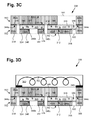
- second patterned conductive carrier 350 may be a fully patterned conductive carrier having top surface 352 and bottom surface 354, and including switch node segment 350a and output segment 350b.
- switch node segment 350a of second patterned conductive carrier 350 is attached to surface 344a of first patterned conductive carrier segment 332a, to control source 314 of control FET 310, and to sync drain 322 of sync FET 320 by electrically coupled die attach material 348.
- output segment 350b of second patterned conductive carrier 350 is attached to surface 344e of first patterned conductive carrier segment 332e by electrically coupled die attach material 348.
- switch node segment 350a and output segment 350b of second patterned conductive carrier 350 may be substantially non-etched.
- switch node segment 350a and output segment 350b of second patterned conductive carrier 350 are shown as connected by dashed lines 356 to indicate that the gaps between those respective segments may be visible in Figures 3C and 3D due to patterning of an initially contiguous conductive carrier structure providing second patterned conductive carrier 350. That is to say, second patterned conductive carrier 350 may be provided by a single conductive carrier support structure, fully patterned to provide switch node segment 350a and output segment 350b. Analogously to first patterned conductive carrier 332, second patterned conductive carrier 350 may be formed of any conductive material having a suitably low electrical resistance. Examples of materials from which second patterned conductive carrier 350 may be formed include Cu, Al, or a conductive alloy. However, in some implementations, it may be advantageous or desirable for second patterned conductive carrier 350 to be implemented as at least a portion of a semiconductor package lead frame.
- switch node segment 350a of second patterned conductive carrier 350 is attached to control source 314, sync drain 322, and surface 344a of first patterned conductive carrier segment 332a using electrically conductive die attach material 348.
- switch node segment 350a of second patterned conductive carrier 350 is configured to electrically couple control source 314 of control FET 310 to sync drain 322 of sync FET 320, as well as to couple control source 314 and sync drain 322 to segment 332a of first patterned conductive carrier 332. Consequently, switch node segment 350a of second patterned conductive carrier 350 and segment 332a of first patterned conductive carrier 332 provide switch node contact 318. It is noted that switch node contact 318 corresponds in general to switch node 118, in Figure 1 , and may share any of the characteristics attributed to that corresponding feature in the present application.
- flowchart 200 may conclude with attaching output inductor 360 over top surface 352 of second patterned conductive carrier 350 (action 238).
- output inductor 360 may be coupled between switch node segment 350a and output segment 350b of second patterned conductive carrier 350 using electrically conductive die attach material 348.
- output inductor 360 includes a core.
- the core may include a magnetic core, for example. More specifically, the core may include a high stability ferrite core. In some implementations, the core may have a cylindrical shape, a ring shape, or another suitable shape.
- the core may include caps, such as circular caps, at each end.
- Output inductor 360 further includes winding 362.
- Winding 362 may include copper, or another suitable conductive material. More specifically, winding 362 may include a high temperature polyurethane copper wire. As shown in Figure 3D , winding 362 includes a first end for coupling to switch node segment 350a of second patterned conductive carrier 350 and a second end for coupling to output segment 350b of second patterned conductive carrier 350.
- output segment 350b of second patterned conductive carrier 350 is attached to surface 344e of first patterned conductive carrier segment 332e by electrically conductive die attach material 348.
- output segment 350b of second patterned conductive carrier 350 and segment 332e of first conductive carrier 332 provide output contact 306.
- output contact 306 corresponds in general to output 106 of power converter 100, in Figure 1 , and may share any of the characteristics attributed to that corresponding feature in the present application.
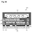
- Figure 4A shows an exemplary representation of a power converter package with integrated output inductor, according to one implementation.
- Figure 4A presents a cross-sectional view of semiconductor package 402A attached to mounting surface 490, which may be a printed circuit board (PCB) for example, by solder bodies 492.
- Semiconductor package 402A includes first patterned conductive carrier 432, which itself includes conductive carrier segments 432a, 432b, 432c, 432d, and 432e (hereinafter "segments 432a-432e"). It is noted that first patterned conductive carrier 432 includes partially etched segments 432b, 432c, and 432d, which may be half-etched, for example, as well as segments 432a and 432e, which may be substantially non-etched.
- first patterned conductive carrier 432 may be a non-contiguous conductive carrier, made up of patterned and disjointed segments 432a-432e that are housed within semiconductor package 402A, and that are in electrical communication only through conductive traces and routing on or within mounting surface 490.
- conductive carrier 432 has a die receiving side, and I/O side 442 opposite the die receiving side and connecting semiconductor package 402A to mounting surface 490.
- Semiconductor package 402A also includes control FET 410 (Q 1 ) having control drain 412, control source 414, and control gate 416, as well as sync FET 420 (Q 2 ) having sync drain 422, sync source 424, and sync gate 426.
- control drain 412 of control FET 410 is attached to recessed surface 446d on the die receiving side of partially etched segment 432d by electrically conductive die attach material 448.
- sync source 424 and sync gate 426 of sync FET 420 are similarly attached to respective recessed surfaces 446b and 446c on the die receiving side of respective partially etched segments 432b and 432c.
- second patterned conductive carrier 450 having top surface 452 and bottom surface 454, and including switch node segment 450a and output segment 450b.
- Switch node segment 450a of second patterned conductive carrier 450 is attached to control source 414 of control FET 410, sync drain 422 of sync FET 420, and surface 444a on the die receiving side of first patterned conductive carrier segment 432a by electrically conductive die attach material 448.
- Semiconductor package 402A further includes integrated output inductor 460 having winding 462, and packaging encapsulant 470.
- output inductor 460 is attached over top surface 452 of second patterned conductive carrier 450 and is coupled between switch node segment 450a and output segment 450b of second patterned conductive 450 using electrically conductive die attach material 448.
- control FET 410 and sync FET 420 are situated between first patterned conductive carrier 432 and second patterned conductive carrier 450, while second patterned conductive carrier 450 is situated between output inductor 460 and control and sync FETS 410 and 420.
- packaging encapsulant 470 may be any suitable dielectric overmolding or encapsulation material typically used in semiconductor packaging, as known in the art.
- switch node segment 450a of second patterned conductive carrier 450 is attached to control source 414, sync drain 422, and surface 444a of first patterned conductive carrier segment 432a using electrically conductive die attach material 448.
- switch node segment 450a of second patterned conductive carrier 450 is configured to electrically couple control source 414 of control FET 410 to sync drain 422 of sync FET 420, as well as to couple control source 414 and sync drain 422 to segment 432a of first patterned conductive carrier 432.
- switch node segment 450a of second patterned conductive carrier 450 and segment 432a of first patterned conductive carrier 432 provide switch node contact 418 of semiconductor package 402A.
- output segment 450b of second patterned conductive carrier 450 and segment 432e of first conductive carrier 432 provide output contact 406 of semiconductor package 402b.
- Semiconductor package 402A including integrated output inductor 460 corresponds in general to output stage 102 including integrated output inductor 160, in Figure 1 , and may share any of the characteristics attributed to that corresponding feature, above.
- switch node contact 418 and output contact 406 correspond respectively to switch node contact 318 and output contact 306 in Figures 3C and 3D , and may share any of the characteristics attributed to those corresponding features, above.
- first and second patterned conductive carriers 432 and 450, control FET 410, sync FET 420, and electrically conductive die attach material 448 correspond respectively in general to first and second patterned conductive carriers 332 and 350, control FET 310, sync FET 320, and electrically conductive die attach material 348, in Figures 3A-3D , and may share any of the characteristics attributed to those corresponding feature, above.
- Figure 4B shows an exemplary representation of a power converter package with integrated output inductor, according to another implementation.
- Figure 4B presents a cross-sectional view of semiconductor package 402B attached to mounting surface 490 by solder bodies 492. It is noted that all features in Figure 4B identified by reference numbers shown in and described by reference to Figure 4A , above, correspond respectively to those features and may share any of the characteristics attributed to those corresponding features in the present application.
- top surface 464 of output inductor 460 is exposed through packaging encapsulant 470 at top surface 484 of semiconductor package 402B.
- exposure of top surface 464 of output inductor 460 at top surface 484 of semiconductor package 402B may result in improved thermal performance by semiconductor package 402B.
- Figure 4C shows an exemplary representation of a power converter package with integrated output inductor, according to another implementation.
- Figure 4C presents a cross-sectional view of semiconductor package 402C attached to mounting surface 490 by solder bodies 492. It is noted that all features in Figure 4C identified by reference numbers shown in and described by reference to Figure 4A and Figure 4B , above, correspond respectively to those features and may share any of the characteristics attributed to those corresponding features in the present application.
- semiconductor package 402C includes second patterned conductive carrier 450 having partially etched switch node segment 450a. That is to say, a portion of switch node segment 450a is partially etched, such as by being half-etched, to provide recessed surface 456 opposite bottom surface 454.
- output inductor 460 may be coupled to top surface 452 of switch node segment 450a at a portion of switch node segment 450a that is substantially non-etched. It is further noted that semiconductor package 402C may be adapted analogously to semiconductor package 402B, in Figure 4B , through exposure of top surface 464 of output inductor 460 at top surface 484 of semiconductor package 402C.
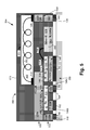
- Figure 5 shows a cross-sectional view of semiconductor package 504 attached to mounting surface 590, which may be a PCB for example, by solder bodies 592.
- Semiconductor package 504 includes first patterned conductive carrier 532, which itself includes conductive carrier segments 532a, 532b, 532c, 532d, 532e, and 532f (hereinafter "segments 532a-532f"). It is noted that first patterned conductive carrier 532 includes partially etched segments 532b, 532c, 532d, and 532e, which may be half-etched, for example, as well as segments 532a and 532f, which may be substantially non-etched.
- first patterned conductive carrier 532 may be a non-contiguous conductive carrier, made up of patterned and disjointed segments 532a-532f that are housed within semiconductor package 504, and that are in electrical communication only through conductive traces and routing on or within mounting surface 590.
- first patterned conductive carrier 532 has a die receiving side, and I/O side 542 opposite the die receiving side and connecting semiconductor package 504 to mounting surface 590.
- Semiconductor package 504 includes control FET 510 (Q 1 ) having control drain 512, control source 514, and control gate 516, as well as sync FET 520 (Q 2 ) having sync drain 522, sync source 524, and sync gate 526.
- control drain 512 of control FET 510 is attached to recessed surface 546d on the die receiving side of partially etched segment 532d by electrically conductive die attach material 548.
- sync source 524 and sync gate 526 of sync FET 520 are similarly attached to respective recessed surfaces 546b and 546c on the die receiving side of respective partially etched segments 532b and 532c.
- Semiconductor package 504 also includes driver IC 528 for driving at least one of control FET 510 and sync FET 520.
- Figure 5 shows one or more wire bonds 586 coupling control gate 516 of control FET 510 to driver IC 528, and die attach material 588.
- die attach material 588 which may be an electrically conductive die attach material or a dielectric die attach material, is used to attach driver IC 528 to recessed surface 546e on the die receiving side of partially etched segment 532e of first patterned conductive carrier 532.
- electrical connection of control gate 516 to driver IC 528 is depicted as being provided by one or more wire bonds 586 in Figure 5 , that representation is merely for the purposes of conceptual clarity. More generally, the electrical connection represented by one or more wire bonds 586 may be implemented using conductive clips, ribbons, or strips, for example.
- second patterned conductive carrier 550 having top surface 552 and bottom surface 554, and including switch node segment 550a and output segment 550b.
- Switch node segment 550a of second patterned conductive carrier 550 is attached to control source 514 of control FET 510, sync drain 522 of sync FET 520, and surface 544a on the die receiving side of first patterned conductive carrier segment 532a by electrically conductive die attach material 548.
- Output segment 550b of second patterned conductive carrier 550 is attached to segment 532f of first patterned conductive carrier 532 by electrically conductive die attach material 548.
- Semiconductor package 504 further includes integrated output inductor 560 having winding 562, and packaging encapsulant 570.
- output inductor 560 is attached over top surface 552 of second patterned conductive carrier 550 and is coupled between switch node segment 550a and output segment 550b of second patterned conductive 550 using electrically conductive die attach material 548.
- control FET 510, sync FET 520, and driver IC 528 are situated between first patterned conductive carrier 532 and second patterned conductive carrier 550
- second patterned conductive carrier 550 is situated between output inductor 560 and control FET 510, sync FET 520, and driver IC 528.
- switch node segment 550a of second patterned conductive carrier 550 is attached to control source 514, sync drain 522, and surface 544a of first patterned conductive carrier segment 532a using electrically conductive die attach material 548.
- switch node segment 550a of second patterned conductive carrier 550 is configured to electrically couple control source 514 of control FET 510 to sync drain 522 of sync FET 520, as well as to couple control source 514 and sync drain 522 to segment 532a of first patterned conductive carrier 532.
- switch node segment 550a of second patterned conductive carrier 550 and segment 532a of first patterned conductive carrier 532 provide switch node contact 518 of semiconductor package 504.
- output segment 550b of second patterned conductive carrier 550 and segment 532f of first conductive carrier 532 provide output contact 506 of semiconductor package 504.
- Semiconductor package 504 including integrated output inductor 560 corresponds in general to power converter package 104 including integrated output inductor 160, in Figure 1 , and may share any of the characteristics attributed to that corresponding feature, above.
- switch node contact 518 and output contact 506, in Figure 5 correspond respectively to switch node contact 418 and output contact 406 in Figures 4A-4C , and may share any of the characteristics attributed to those corresponding features, above.
- first and second patterned conductive carriers 532 and 550, control FET 510, and sync FET 520 correspond respectively in general to first and second patterned conductive carriers 432 and 450, control FET 410, and sync FET 420, in Figures 4A-4C , and may share any of the characteristics attributed to those corresponding feature, above.
- first patterned conductive carrier 532 and/or second patterned conductive carrier 550 may each be implemented using at least a portion of a semiconductor package lead frame.
- electrically conductive die attach material 548 and packaging encapsulant 570 correspond respectively in general to electrically conductive die attach material 448 and packaging encapsulant 470, in Figures 4A-4C , and may share any of the characteristics attributed to those corresponding features, above.
- exemplary semiconductor package 504 may be readily adapted to include the alternative features shown in Figures 4B and 4C .
- top surface 564 of output capacitor may be exposed at top surface 584 of semiconductor package 504, and/or switch node segment 550a of second patterned conductive carrier 550 may be partially etched, as described above.
- the present application discloses a packaging solution with integrated output inductor that provides a highly compact design for packaging a power converter, such as a voltage regulator.
- a power converter such as a voltage regulator.
Landscapes
- Engineering & Computer Science (AREA)
- Power Engineering (AREA)
- Dc-Dc Converters (AREA)
- Microelectronics & Electronic Packaging (AREA)
Abstract
Description
- The present application claims the benefit of and priority to a provisional application entitled "Package with Inductor on Powerstage," Serial No.
62/061,623 filed on October 8, 2014 - Power converters, such as voltage regulators, are used in a variety of electronic circuits and systems. Many integrated circuit (IC) applications, for instance, require conversion of a direct current (DC) input voltage to a lower, or higher, DC output voltage. For example, a buck converter may be implemented to convert a higher voltage DC input to a lower voltage DC output for use in low voltage applications in which relatively large output currents are required.
- The output stage of a power converter typically includes a high side control transistor and a low side synchronous (sync) transistor, and may include a relatively large output inductor. In addition, power converter circuitry typically includes a driver IC designed to drive the control and/or sync transistors of the output stage. Consequently, packaging solutions for a power converter typically require printed circuit board (PCB) area sufficient to accommodate a side-by-side layout including not only the control and sync transistors of the power converter output stage, but the output inductor and the driver IC for the output stage as well.
- The present disclosure is directed to a power converter package with integrated output inductor, substantially as shown in and/or described in connection with at least one of the figures, and as set forth in the claims.
-
-
Figure 1 shows a diagram of an exemplary power converter. -
Figure 2 shows a flowchart presenting an exemplary method for fabricating a power converter package with integrated output inductor, according to one implementation. -
Figures 3A illustrates a result of performing an initial action according to the exemplary flowchart ofFigure 2 in accordance with one implementation. -
Figures 3B illustrates a result of performing a subsequent action according to the exemplary flowchart ofFigure 2 in accordance with one implementation. -
Figures 3C illustrates a result of performing a subsequent action according to the exemplary flowchart ofFigure 2 in accordance with one implementation. -
Figures 3D illustrates a result of performing a final action according to the exemplary flowchart ofFigure 2 in accordance with one implementation. -
Figure 4A shows an exemplary representation of a power converter package with integrated output inductor, according to one implementation. -
Figure 4B shows an exemplary representation of a power converter package with integrated output inductor, according to another implementation. -
Figure 4C shows an exemplary representation of a power converter package with integrated output inductor, according to another implementation. -
Figure 5 shows an exemplary representation of a power converter package with integrated output inductor, according to yet another implementation. - The following description contains specific information pertaining to implementations in the present disclosure. One skilled in the art will recognize that the present disclosure may be implemented in a manner different from that specifically discussed herein. The drawings in the present application and their accompanying detailed description are directed to merely exemplary implementations. Unless noted otherwise, like or corresponding elements among the figures may be indicated by like or corresponding reference numerals. Moreover, the drawings and illustrations in the present application are generally not to scale, and are not intended to correspond to actual relative dimensions.
- As stated above, power converters, such as voltage regulators, are used in a variety of electronic circuits and systems. For instance, integrated circuit (IC) applications may require conversion of a direct current (DC) input voltage to a lower, or higher, DC output voltage. As a specific example, a buck converter may be implemented as a voltage regulator to convert a higher voltage DC input to a lower voltage DC output for use in low voltage applications in which relatively large output currents are required.
-
Figure 1 shows a diagram of an exemplary power converter.Power converter 100 includespower converter package 104 andoutput capacitor 108. As shown inFigure 1 ,power converter package 104 includesoutput stage 102 ofpower converter 100, anddriver IC 128 providing drive signals tooutput stage 102. As further shown inFigure 1 ,power converter 100 is configured to receive an input voltage VIN, and to provide a converted voltage, e.g., a rectified and/or stepped down voltage, as VOUT atoutput 106. -
Output stage 102 may be implemented using two power switches in the form of metal-oxide-semiconductor field-effect transistors (MOSFETs) configured as a half bridge, for example. That is to say,output stage 102 may include high side or control FET 110 (Q1) havingdrain 112,source 114, andgate 116, as well as low side or synchronous (sync) FET 120 (Q2) havingdrain 122,source 124, andgate 126. In addition,output stage 102 ofpower converter package 104 includesintegrated output inductor 160. As shown inFigure 1 ,control FET 110 is coupled tosync FET 120 atswitch node 118, which, in turn, is coupled tooutput 106 throughoutput inductor 160. Respective control and sync FETs 110 and 120 may be implemented as group IV based power FETs, such as silicon power MOSFETs having a vertical design, for example.Power converter 100 may be advantageously utilized, for example as a buck converter, in a variety of automotive, industrial, appliance, and lighting applications. - It is noted that in the interests of ease and conciseness of description, the present inventive principles will in some instances be described by reference to specific implementations of a buck converter including one or more silicon based power FETs. However, it is emphasized that such implementations are merely exemplary, and the inventive principles disclosed herein are broadly applicable to a wide range of applications, including buck and boost converters, implemented using other group IV material based, or group III-V semiconductor based, power transistors.
- It is further noted that as used herein, the phrase "group III-V" refers to a compound semiconductor including at least one group III element and at least one group V element. By way of example, a group III-V semiconductor may take the form of a III-Nitride semiconductor that includes nitrogen and at least one group III element. For instance, a III-Nitride power FET may be fabricated using gallium nitride (GaN), in which the group III element or elements include some or a substantial amount of gallium, but may also include other group III elements in addition to gallium. Thus, in some implementations, one or both of
control FET 110 and sync FET 120 may take the form of a III-Nitride power FET, such as a III-Nitride high electron mobility transistor (HEMT). - Continuing to
Figure 2, Figure 2 showsflowchart 200 presenting an exemplary method for fabricating a power converter package with integrated output inductor. The exemplary method described byflowchart 200 is performed on a portion of a conductive carrier structure, which may be a semiconductor package lead frame, or may take the form of a conductive sheet or plate, for example. - With respect to
Figures 3A-3D ,structures flowchart 200, according to one implementation. For example,Figure 3A represents first patternedconductive carrier 332 includingsegments segments 332a-332e"), and having diereceiving side 340 and opposite input/output (I/O) side 342 (action 232).Structure 334 shows first patternedconductive carrier 332 after attachment of a control FET and a sync FET to partially etchedsegments Structure 336 showsstructure 334 after attachment of a second patterned conductive carrier (action 236), and so forth. - Referring to
flowchart 200, inFigure 2 , in combination withFigure 3A ,flowchart 200 begins with providing first patternedconductive carrier 332 having die receivingside 340, and opposite I/O side 342 (action 232). As shown inFigure 3A , first patternedconductive carrier 332 may be a fully patterned conductive carrier includingconductive carrier segments 332a-332e. As further shown inFigure 3A , first patternedconductive carrier 332 is shown to havesurfaces respective segments recessed surfaces segments segments segments - It is noted that
segments 332a-332e are shown as connected bydashed lines 330 to indicate that the gaps between those respective segments may be visible inFigures 3A-3D due to patterning of an initially contiguous conductive carrier structure providing first patternedconductive carrier 332. That is to say, first patternedconductive carrier 332 may be provided by a single conductive carrier support structure, fully patterned to providesegments 332a-332e. First patternedconductive carrier 332 may be formed of any conductive material having a suitably low electrical resistance. Examples of materials from which first patternedconductive carrier 332 may be formed include copper (Cu), aluminum (Al), or a conductive alloy. In one implementation, as noted above, first patternedconductive carrier 332 may be implemented using at least a portion of a semiconductor package lead frame. - Recessed
surfaces receiving side 340 of first patternedconductive carrier 332 may be the result of a partial etch performed on die receivingside 340, resulting in formation of partially etchedsegments recessed surfaces conductive carrier 332, on diereceiving side 340, to form half-etched segments corresponding to partially etchedsegments - Although not shown in the present figures, in some implementations, patterned
conductive carrier 332 may include a barrier metal layer formed on one or both ofdie receiving side 340 and I/O side 342. Such a barrier metal layer may be formed of nickel-gold (NiAu) or nickel-palladium-gold (NiPdAu), for example. In some implementations, such a barrier metal layer may serve as an etching mask during patterning of first patternedconductive carrier 332. - Moving to structure 334 in
Figure 3B with ongoing reference toFigure 2 ,flowchart 200 continues with attaching control FET 310 (Q1) and sync FET 320 (Q2) to partially etched segments of first patterned conductive carrier 332 (action 234).Control FET 310 includescontrol drain 312,control source 314, andcontrol gate 316, whilesync FET 320 includessync drain 322,sync source 324, andsync gate 326. As shown inFigure 3B ,control drain 312 ofcontrol FET 310 is attached to recessedsurface 346d on die receivingside 340 of partially etchedsegment 332d of first patternedconductive carrier 332 by electrically conductive die attachmaterial 348. As further shown inFigure 3B ,sync source 324 andsync gate 326 ofsync FET 320 are attached to recessedsurfaces side 340 of respective partially etchedsegments 332b and 332c of first patternedconductive carrier 332 by electrically conductive die attachmaterial 348. - Electrically conductive die attach
material 348 may be any suitable substance, such as a conductive epoxy, solder, a conductive sintered material, or a diffusion bonded material, formed to a thickness of approximately 10 µm or greater, for example.Control FET 310 and syncFET 320 are shown as power FETs having a vertical topology. That is to say, controlsource 314 andcontrol gate 316 are situated on the same side ofcontrol FET 310, while control drain 312 is situated on an opposite side ofcontrol FET 310. Similarly,sync source 324 andsync gate 326 are situated on the same side ofsync FET 320, whilesync drain 322 is situated on an opposite side ofsync FET 320. - In one implementation, respective control and sync
FETs FETs FETs - It is noted that
control FET 310 and syncFET 320 are flipped relative to each other. That is to say,control FET 310 is disposed on recessedsurface 346d of partially etchedsegment 332d in a "face up" orientation in which control drain 312 is attached to recessedsurface 346d, whilesync FET 320 is oriented "face down" such thatsync source 324 andsync gate 326 are attached to recessedsurfaces segments 332c and 332b. - It is further noted that control and sync
FETs conductive carrier 332 in any temporal order. Thus,control FET 310 may be attached to first patternedconductive carrier 332 before or after attachment ofsync FET 320 to first patterned conductive carrier. Moreover, in some implementations, control and syncFETs conductive carrier 332 substantially concurrently. -
Control FET 310 having control drain 312,control source 314, andcontrol gate 316 corresponds in general to controlFET 110 havingdrain 112,source 114, andgate 116, inFigure 1 , and may share any of the characteristics attributed to that corresponding feature in the present application. In addition,sync FET 320 having sync drain 322,sync source 324, andsync gate 326 corresponds in general to syncFET 120 havingdrain 122,source 124, andgate 126, inFigure 1 , and may share any of the characteristics attributed to that corresponding feature in the present application. - Referring to structure 336 in
Figure 3C ,flowchart 200 continues with attaching second patternedconductive carrier 350 over first patternedconductive carrier 332,control FET 310, and sync FET 320 (action 236). As shown inFigure 3C , second patternedconductive carrier 350 may be a fully patterned conductive carrier havingtop surface 352 andbottom surface 354, and includingswitch node segment 350a andoutput segment 350b. - As further shown in
Figure 3C ,switch node segment 350a of second patternedconductive carrier 350 is attached to surface 344a of first patternedconductive carrier segment 332a, to controlsource 314 ofcontrol FET 310, and to syncdrain 322 ofsync FET 320 by electrically coupled die attachmaterial 348. In addition,output segment 350b of second patternedconductive carrier 350 is attached to surface 344e of first patternedconductive carrier segment 332e by electrically coupled die attachmaterial 348. According to the implementation shown inFigure 3C , for example,switch node segment 350a andoutput segment 350b of second patternedconductive carrier 350 may be substantially non-etched. - It is noted that
switch node segment 350a andoutput segment 350b of second patternedconductive carrier 350 are shown as connected by dashedlines 356 to indicate that the gaps between those respective segments may be visible inFigures 3C and 3D due to patterning of an initially contiguous conductive carrier structure providing second patternedconductive carrier 350. That is to say, second patternedconductive carrier 350 may be provided by a single conductive carrier support structure, fully patterned to provideswitch node segment 350a andoutput segment 350b. Analogously to first patternedconductive carrier 332, second patternedconductive carrier 350 may be formed of any conductive material having a suitably low electrical resistance. Examples of materials from which second patternedconductive carrier 350 may be formed include Cu, Al, or a conductive alloy. However, in some implementations, it may be advantageous or desirable for second patternedconductive carrier 350 to be implemented as at least a portion of a semiconductor package lead frame. - As shown in
Figure 3C and noted above,switch node segment 350a of second patternedconductive carrier 350 is attached to controlsource 314,sync drain 322, andsurface 344a of first patternedconductive carrier segment 332a using electrically conductive die attachmaterial 348. As a result,switch node segment 350a of second patternedconductive carrier 350 is configured to electricallycouple control source 314 ofcontrol FET 310 to sync drain 322 ofsync FET 320, as well as to couplecontrol source 314 andsync drain 322 tosegment 332a of first patternedconductive carrier 332. Consequently,switch node segment 350a of second patternedconductive carrier 350 andsegment 332a of first patternedconductive carrier 332 provideswitch node contact 318. It is noted thatswitch node contact 318 corresponds in general to switchnode 118, inFigure 1 , and may share any of the characteristics attributed to that corresponding feature in the present application. - Continuing to structure 338 in
Figure 3D ,flowchart 200 may conclude with attachingoutput inductor 360 overtop surface 352 of second patterned conductive carrier 350 (action 238). As shown inFigure 3D ,output inductor 360 may be coupled betweenswitch node segment 350a andoutput segment 350b of second patternedconductive carrier 350 using electrically conductive die attachmaterial 348. - In one implementation,
output inductor 360 includes a core. The core may include a magnetic core, for example. More specifically, the core may include a high stability ferrite core. In some implementations, the core may have a cylindrical shape, a ring shape, or another suitable shape. The core may include caps, such as circular caps, at each end. -
Output inductor 360 further includes winding 362. Winding 362 may include copper, or another suitable conductive material. More specifically, winding 362 may include a high temperature polyurethane copper wire. As shown inFigure 3D , winding 362 includes a first end for coupling to switchnode segment 350a of second patternedconductive carrier 350 and a second end for coupling tooutput segment 350b of second patternedconductive carrier 350. - Moreover, and as noted above,
output segment 350b of second patternedconductive carrier 350 is attached to surface 344e of first patternedconductive carrier segment 332e by electrically conductive die attachmaterial 348. As a result,output segment 350b of second patternedconductive carrier 350 andsegment 332e of firstconductive carrier 332 provideoutput contact 306. It is noted thatoutput contact 306 corresponds in general tooutput 106 ofpower converter 100, inFigure 1 , and may share any of the characteristics attributed to that corresponding feature in the present application. - Moving to
Figure 4A, Figure 4A shows an exemplary representation of a power converter package with integrated output inductor, according to one implementation.Figure 4A presents a cross-sectional view ofsemiconductor package 402A attached to mountingsurface 490, which may be a printed circuit board (PCB) for example, bysolder bodies 492.Semiconductor package 402A includes first patternedconductive carrier 432, which itself includesconductive carrier segments segments 432a-432e"). It is noted that first patternedconductive carrier 432 includes partially etchedsegments segments - As shown in
Figure 4A , first patternedconductive carrier 432 may be a non-contiguous conductive carrier, made up of patterned anddisjointed segments 432a-432e that are housed withinsemiconductor package 402A, and that are in electrical communication only through conductive traces and routing on or within mountingsurface 490. As further shown inFigure 4A ,conductive carrier 432 has a die receiving side, and I/O side 442 opposite the die receiving side and connectingsemiconductor package 402A to mountingsurface 490. -
Semiconductor package 402A also includes control FET 410 (Q1) having control drain 412,control source 414, andcontrol gate 416, as well as sync FET 420 (Q2) having sync drain 422,sync source 424, andsync gate 426. As shown inFigure 4A ,control drain 412 ofcontrol FET 410 is attached to recessedsurface 446d on the die receiving side of partially etchedsegment 432d by electrically conductive die attachmaterial 448. In addition,sync source 424 andsync gate 426 ofsync FET 420 are similarly attached to respective recessedsurfaces segments 432b and 432c. - Also shown in
Figure 4A is second patternedconductive carrier 450 havingtop surface 452 andbottom surface 454, and includingswitch node segment 450a andoutput segment 450b.Switch node segment 450a of second patternedconductive carrier 450 is attached to controlsource 414 ofcontrol FET 410,sync drain 422 ofsync FET 420, andsurface 444a on the die receiving side of first patternedconductive carrier segment 432a by electrically conductive die attachmaterial 448. -
Semiconductor package 402A further includesintegrated output inductor 460 having winding 462, andpackaging encapsulant 470. As shown inFigure 4A ,output inductor 460 is attached overtop surface 452 of second patternedconductive carrier 450 and is coupled betweenswitch node segment 450a andoutput segment 450b of second patterned conductive 450 using electrically conductive die attachmaterial 448. Thus,control FET 410 and syncFET 420 are situated between first patternedconductive carrier 432 and second patternedconductive carrier 450, while second patternedconductive carrier 450 is situated betweenoutput inductor 460 and control and sync FETS 410 and 420. It is noted thatpackaging encapsulant 470 may be any suitable dielectric overmolding or encapsulation material typically used in semiconductor packaging, as known in the art. - As noted above, according to the implementation shown in
Figure 4A ,switch node segment 450a of second patternedconductive carrier 450 is attached to controlsource 414,sync drain 422, andsurface 444a of first patternedconductive carrier segment 432a using electrically conductive die attachmaterial 448. As a result,switch node segment 450a of second patternedconductive carrier 450 is configured to electricallycouple control source 414 ofcontrol FET 410 to sync drain 422 ofsync FET 420, as well as to couplecontrol source 414 andsync drain 422 tosegment 432a of first patternedconductive carrier 432. Consequently,switch node segment 450a of second patternedconductive carrier 450 andsegment 432a of first patternedconductive carrier 432 provideswitch node contact 418 ofsemiconductor package 402A. Moreover,output segment 450b of second patternedconductive carrier 450 andsegment 432e of firstconductive carrier 432 provideoutput contact 406 of semiconductor package 402b. -
Semiconductor package 402A includingintegrated output inductor 460 corresponds in general tooutput stage 102 includingintegrated output inductor 160, inFigure 1 , and may share any of the characteristics attributed to that corresponding feature, above. In addition,switch node contact 418 andoutput contact 406 correspond respectively to switchnode contact 318 andoutput contact 306 inFigures 3C and 3D , and may share any of the characteristics attributed to those corresponding features, above. Moreover, first and second patternedconductive carriers control FET 410,sync FET 420, and electrically conductive die attachmaterial 448, correspond respectively in general to first and second patternedconductive carriers control FET 310,sync FET 320, and electrically conductive die attachmaterial 348, inFigures 3A-3D , and may share any of the characteristics attributed to those corresponding feature, above. - Continuing to
Figure 4B, Figure 4B shows an exemplary representation of a power converter package with integrated output inductor, according to another implementation.Figure 4B presents a cross-sectional view ofsemiconductor package 402B attached to mountingsurface 490 bysolder bodies 492. It is noted that all features inFigure 4B identified by reference numbers shown in and described by reference toFigure 4A , above, correspond respectively to those features and may share any of the characteristics attributed to those corresponding features in the present application. - In contrast to the exemplary packaging solution shown in
Figure 4A , however,top surface 464 ofoutput inductor 460 is exposed throughpackaging encapsulant 470 attop surface 484 ofsemiconductor package 402B. In some implementations, exposure oftop surface 464 ofoutput inductor 460 attop surface 484 ofsemiconductor package 402B may result in improved thermal performance bysemiconductor package 402B. - Referring to
Figure 4C, Figure 4C shows an exemplary representation of a power converter package with integrated output inductor, according to another implementation.Figure 4C presents a cross-sectional view ofsemiconductor package 402C attached to mountingsurface 490 bysolder bodies 492. It is noted that all features inFigure 4C identified by reference numbers shown in and described by reference toFigure 4A andFigure 4B , above, correspond respectively to those features and may share any of the characteristics attributed to those corresponding features in the present application. - In contrast to
semiconductor packages Figures 4A and4B , however,semiconductor package 402C includes second patternedconductive carrier 450 having partially etchedswitch node segment 450a. That is to say, a portion ofswitch node segment 450a is partially etched, such as by being half-etched, to provide recessedsurface 456 oppositebottom surface 454. - It is noted that, according to the implementation shown in
Figure 4C ,output inductor 460 may be coupled totop surface 452 ofswitch node segment 450a at a portion ofswitch node segment 450a that is substantially non-etched. It is further noted thatsemiconductor package 402C may be adapted analogously tosemiconductor package 402B, inFigure 4B , through exposure oftop surface 464 ofoutput inductor 460 attop surface 484 ofsemiconductor package 402C. - The implementations shown and described by reference to
Figures 4A-4C result inrespective semiconductor packages 402A-402C configured to encloseoutput stage 102, inFigure 1 . However, in some applications, it may be advantageous or desirable to produce a semiconductor package corresponding topower converter package 104. An example implementation of such a semiconductor package is shown byFigure 5 . One of ordinary skill in the art will readily understand that the exemplary method outlined byflowchart 200, inFigure 2 , can be suitably adapted to produce the exemplary semiconductor package shown inFigure 5 . -
Figure 5 shows a cross-sectional view ofsemiconductor package 504 attached to mountingsurface 590, which may be a PCB for example, bysolder bodies 592.Semiconductor package 504 includes first patternedconductive carrier 532, which itself includesconductive carrier segments segments 532a-532f"). It is noted that first patternedconductive carrier 532 includes partially etchedsegments 532b, 532c, 532d, and 532e, which may be half-etched, for example, as well assegments 532a and 532f, which may be substantially non-etched. - As shown in
Figure 5 , first patternedconductive carrier 532 may be a non-contiguous conductive carrier, made up of patterned anddisjointed segments 532a-532f that are housed withinsemiconductor package 504, and that are in electrical communication only through conductive traces and routing on or within mountingsurface 590. As further shown inFigure 5 , first patternedconductive carrier 532 has a die receiving side, and I/O side 542 opposite the die receiving side and connectingsemiconductor package 504 to mountingsurface 590. -
Semiconductor package 504 includes control FET 510 (Q1) having control drain 512,control source 514, andcontrol gate 516, as well as sync FET 520 (Q2) having sync drain 522,sync source 524, and sync gate 526. As shown inFigure 5 ,control drain 512 ofcontrol FET 510 is attached to recessed surface 546d on the die receiving side of partially etched segment 532d by electrically conductive die attachmaterial 548. In addition,sync source 524 and sync gate 526 ofsync FET 520 are similarly attached to respective recessedsurfaces segments 532b and 532c. -
Semiconductor package 504 also includesdriver IC 528 for driving at least one ofcontrol FET 510 and syncFET 520. In addition,Figure 5 shows one ormore wire bonds 586coupling control gate 516 ofcontrol FET 510 todriver IC 528, and die attachmaterial 588. It is noted that die attachmaterial 588, which may be an electrically conductive die attach material or a dielectric die attach material, is used to attachdriver IC 528 to recessedsurface 546e on the die receiving side of partially etched segment 532e of first patternedconductive carrier 532. It is further noted that although electrical connection ofcontrol gate 516 todriver IC 528 is depicted as being provided by one ormore wire bonds 586 inFigure 5 , that representation is merely for the purposes of conceptual clarity. More generally, the electrical connection represented by one ormore wire bonds 586 may be implemented using conductive clips, ribbons, or strips, for example. - Also shown in
Figure 5 is second patternedconductive carrier 550 havingtop surface 552 andbottom surface 554, and includingswitch node segment 550a andoutput segment 550b.Switch node segment 550a of second patternedconductive carrier 550 is attached to controlsource 514 ofcontrol FET 510,sync drain 522 ofsync FET 520, and surface 544a on the die receiving side of first patternedconductive carrier segment 532a by electrically conductive die attachmaterial 548.Output segment 550b of second patternedconductive carrier 550 is attached to segment 532f of first patternedconductive carrier 532 by electrically conductive die attachmaterial 548. -
Semiconductor package 504 further includesintegrated output inductor 560 having winding 562, andpackaging encapsulant 570. As shown inFigure 5 ,output inductor 560 is attached overtop surface 552 of second patternedconductive carrier 550 and is coupled betweenswitch node segment 550a andoutput segment 550b of second patterned conductive 550 using electrically conductive die attachmaterial 548. Thus,control FET 510,sync FET 520, anddriver IC 528 are situated between first patternedconductive carrier 532 and second patternedconductive carrier 550, while second patternedconductive carrier 550 is situated betweenoutput inductor 560 and controlFET 510,sync FET 520, anddriver IC 528. Also shown inFigure 5 aretop surface 564 ofoutput inductor 560 andtop surface 584 ofsemiconductor package 504. - As noted above, according to the implementation shown in
Figure 5 ,switch node segment 550a of second patternedconductive carrier 550 is attached to controlsource 514,sync drain 522, and surface 544a of first patternedconductive carrier segment 532a using electrically conductive die attachmaterial 548. As a result,switch node segment 550a of second patternedconductive carrier 550 is configured to electricallycouple control source 514 ofcontrol FET 510 to sync drain 522 ofsync FET 520, as well as to couplecontrol source 514 andsync drain 522 tosegment 532a of first patternedconductive carrier 532. Consequently,switch node segment 550a of second patternedconductive carrier 550 andsegment 532a of first patternedconductive carrier 532 provideswitch node contact 518 ofsemiconductor package 504. Moreover,output segment 550b of second patternedconductive carrier 550 and segment 532f of firstconductive carrier 532 provideoutput contact 506 ofsemiconductor package 504. -
Semiconductor package 504 includingintegrated output inductor 560 corresponds in general topower converter package 104 includingintegrated output inductor 160, inFigure 1 , and may share any of the characteristics attributed to that corresponding feature, above. In addition,switch node contact 518 andoutput contact 506, inFigure 5 , correspond respectively to switchnode contact 418 andoutput contact 406 inFigures 4A-4C , and may share any of the characteristics attributed to those corresponding features, above. - Moreover, first and second patterned
conductive carriers control FET 510, and syncFET 520 correspond respectively in general to first and second patternedconductive carriers control FET 410, and syncFET 420, inFigures 4A-4C , and may share any of the characteristics attributed to those corresponding feature, above. In other words, first patternedconductive carrier 532 and/or second patternedconductive carrier 550 may each be implemented using at least a portion of a semiconductor package lead frame. Furthermore, electrically conductive die attachmaterial 548 andpackaging encapsulant 570, inFigure 5 , correspond respectively in general to electrically conductive die attachmaterial 448 andpackaging encapsulant 470, inFigures 4A-4C , and may share any of the characteristics attributed to those corresponding features, above. - It is noted that
exemplary semiconductor package 504 may be readily adapted to include the alternative features shown inFigures 4B and4C . In other words, in some implementations,top surface 564 of output capacitor may be exposed attop surface 584 ofsemiconductor package 504, and/or switchnode segment 550a of second patternedconductive carrier 550 may be partially etched, as described above. - Thus, the present application discloses a packaging solution with integrated output inductor that provides a highly compact design for packaging a power converter, such as a voltage regulator. By coupling the output inductor between a switch node segment and an output segment of a patterned conductive carrier attached over control and sync FETs, the implementations disclosed herein enable a substantial reduction in PCB surface area required to implement the power converter.
- From the above description it is manifest that various techniques can be used for implementing the concepts described in the present application without departing from the scope of those concepts. Moreover, while the concepts have been described with specific reference to certain implementations, a person of ordinary skill in the art would recognize that changes can be made in form and detail without departing from the scope of those concepts. As such, the described implementations are to be considered in all respects as illustrative and not restrictive. It should also be understood that the present application is not limited to the particular implementations described herein, but many rearrangements, modifications, and substitutions are possible without departing from the scope of the present disclosure.
Claims (15)
- A semiconductor package comprising:a first patterned conductive carrier;a control FET having a control drain attached to a first partially etched segment of said first patterned conductive carrier;a sync FET having a sync source and a sync gate attached to respective second and third partially etched segments of said first patterned conductive carrier;a second patterned conductive carrier having a switch node segment situated over a control source of said control FET and over a sync drain of said sync FET;an inductor coupled between said switch node segment and an output segment of said second patterned conductive carrier.
- The semiconductor package of claim 1, wherein said first, second, and third partially etched segments of said first patterned conductive carrier are substantially half-etched.
- The semiconductor package of claim 1, wherein said switch node segment of said second patterned conductive carrier is partially etched.
- The semiconductor package of claim 1, wherein said control FET, said sync FET, and said inductor form an output stage of a power converter.
- The semiconductor package of claim 1, wherein at least one of said first patterned conductive carrier and said second patterned conductive carrier comprises at least a portion of a lead frame.
- The semiconductor package of claim 1, wherein said second patterned conductive carrier comprises at least a portion of a lead frame.
- The semiconductor package of claim 1, wherein said control FET and said sync FET comprise silicon power FETs.
- The semiconductor package of claim 1, wherein said control FET and said sync FET comprise III-Nitride FETs.
- The semiconductor package of claim 1, wherein said control FET and said sync FET comprise III-Nitride high electron mobility transistors (HEMTs).
- The semiconductor package of claim 1, further comprising a driver integrated circuit for driving at least one of said control FET and said sync FET.
- A method for fabricating a semiconductor package, said method comprising:providing a first patterned conductive carrier;attaching a control drain of a control FET to a first partially etched segment of said first patterned conductive carrier;attaching a sync source and a sync gate of a sync FET to respective second and third partially etched segments of said first patterned conductive carrier;attaching a second patterned conductive carrier having a switch node segment for electrically coupling a control source of said control FET to a sync drain of said sync FET;coupling an inductor between said switch node segment and an output segment of said second patterned conductive carrier.
- The method of claim 11, wherein said first, second, and third partially etched segments of said first patterned conductive carrier are substantially half-etched.
- The method of claim 11, wherein said switch node segment of said second patterned conductive carrier is partially etched.
- The method of claim 11, wherein said control FET, said sync FET, and said inductor form an output stage of a power converter.
- The method of claim 11, wherein at least one of said first patterned conductive carrier and said second patterned conductive carrier comprises at least a portion of a lead frame.
Applications Claiming Priority (2)
| Application Number | Priority Date | Filing Date | Title |
|---|---|---|---|
| US201462061623P | 2014-10-08 | 2014-10-08 | |
| US14/855,665 US9515014B2 (en) | 2014-10-08 | 2015-09-16 | Power converter package with integrated output inductor |
Publications (2)
| Publication Number | Publication Date |
|---|---|
| EP3007223A1 true EP3007223A1 (en) | 2016-04-13 |
| EP3007223B1 EP3007223B1 (en) | 2021-11-10 |
Family
ID=54196799
Family Applications (1)
| Application Number | Title | Priority Date | Filing Date |
|---|---|---|---|
| EP15185987.3A Active EP3007223B1 (en) | 2014-10-08 | 2015-09-21 | Power converter package with integrated output inductor |
Country Status (2)
| Country | Link |
|---|---|
| US (2) | US9515014B2 (en) |
| EP (1) | EP3007223B1 (en) |
Cited By (5)
| Publication number | Priority date | Publication date | Assignee | Title |
|---|---|---|---|---|
| CN107769555A (en) * | 2016-08-22 | 2018-03-06 | 英飞凌科技美国公司 | Power converter with least five electrical connection sections on side |
| CN112684726A (en) * | 2019-10-17 | 2021-04-20 | 英飞凌科技股份有限公司 | Embedded substrate voltage regulator |
| US11071206B2 (en) | 2019-10-17 | 2021-07-20 | Infineon Technologies Austria Ag | Electronic system and processor substrate having an embedded power device module |
| US11147165B2 (en) | 2019-10-17 | 2021-10-12 | Infineon Technologies Austria Ag | Electronic system and interposer having an embedded power device module |
| DE102017214248B4 (en) | 2016-08-22 | 2022-08-04 | Infineon Technologies Americas Corp. | Apparatus having a power stage attached to an inductive element and method of making same |
Families Citing this family (10)
| Publication number | Priority date | Publication date | Assignee | Title |
|---|---|---|---|---|
| US9515014B2 (en) | 2014-10-08 | 2016-12-06 | Infineon Technologies Americas Corp. | Power converter package with integrated output inductor |
| US9565768B2 (en) | 2015-03-25 | 2017-02-07 | Infineon Technologies Americas Corp. | Semiconductor package with integrated output inductor on a printed circuit board |
| US10069417B2 (en) * | 2016-01-04 | 2018-09-04 | Kinetic Technologies | Power conversion device with integrated discrete inductor |
| US10396046B2 (en) | 2017-12-29 | 2019-08-27 | Intel Corporation | Substrate assembly with magnetic feature |
| US10886201B2 (en) * | 2018-02-15 | 2021-01-05 | Epistar Corporation | Power device having a substrate with metal layers exposed at surfaces of an insulation layer and manufacturing method thereof |
| US10818646B2 (en) * | 2019-02-13 | 2020-10-27 | Infineon Technologies Ag | Power stage device with carrier frame for power stage module and integrated inductor |
| US20210082790A1 (en) * | 2019-09-18 | 2021-03-18 | Alpha And Omega Semiconductor (Cayman) Ltd. | Power semiconductor package having integrated inductor and method of making the same |
| US11050355B2 (en) * | 2019-10-17 | 2021-06-29 | Infineon Technologies Austria Ag | Stacked power supply topologies and inductor devices |
| US20240030820A1 (en) * | 2022-07-21 | 2024-01-25 | Infineon Technologies Ag | Modular power device package embedded in circuit carrier |
| WO2025032244A1 (en) * | 2023-08-10 | 2025-02-13 | Lotus Microsystems Aps | Stacked power converter assembly with thermally conductive elements |
Citations (6)
| Publication number | Priority date | Publication date | Assignee | Title |
|---|---|---|---|---|
| US20110134613A1 (en) * | 2009-12-07 | 2011-06-09 | Intersil Americas Inc. | Stacked inductor-electronic package assembly and technique for manufacturing same |
| US20110210708A1 (en) * | 2010-03-01 | 2011-09-01 | Texas Instruments Incorporated | High Frequency Power Supply Module Having High Efficiency and High Current |
| US20110228507A1 (en) * | 2010-03-16 | 2011-09-22 | Intersil Americas Inc. | Molded power-supply module with bridge inductor over other components |
| US20120194148A1 (en) * | 2011-01-28 | 2012-08-02 | Ho-Yin Yiu | Power module and the method of packaging the same |
| US20120200281A1 (en) * | 2011-02-07 | 2012-08-09 | Texas Instruments Incorporated | Three-Dimensional Power Supply Module Having Reduced Switch Node Ringing |
| US20130249051A1 (en) * | 2012-03-23 | 2013-09-26 | Texas Instruments Incorporated | Packaged Semiconductor Device Having Multilevel Leadframes Configured as Modules |
Family Cites Families (19)
| Publication number | Priority date | Publication date | Assignee | Title |
|---|---|---|---|---|
| US6549071B1 (en) * | 2000-09-12 | 2003-04-15 | Silicon Laboratories, Inc. | Power amplifier circuitry and method using an inductance coupled to power amplifier switching devices |
| US8049312B2 (en) * | 2009-01-12 | 2011-11-01 | Texas Instruments Incorporated | Semiconductor device package and method of assembly thereof |
| US20120326287A1 (en) * | 2011-06-27 | 2012-12-27 | National Semiconductor Corporation | Dc/dc convertor power module package incorporating a stacked controller and construction methodology |
| US8450149B2 (en) * | 2009-10-16 | 2013-05-28 | Texas Instruments Incorporated | Stacked leadframe implementation for DC/DC convertor power module incorporating a stacked controller and stacked leadframe construction methodology |
| US9362215B2 (en) * | 2010-12-13 | 2016-06-07 | Infineon Technologies Americas Corp. | Power quad flat no-lead (PQFN) semiconductor package with leadframe islands for multi-phase power inverter |
| US9088215B2 (en) * | 2011-06-08 | 2015-07-21 | Futurewei Technologies, Inc. | Power converter package structure and method |
| US9209176B2 (en) * | 2011-12-07 | 2015-12-08 | Transphorm Inc. | Semiconductor modules and methods of forming the same |
| US9171784B2 (en) * | 2012-03-28 | 2015-10-27 | International Rectifier Corporation | Dual power converter package using external driver IC |
| US9111776B2 (en) * | 2012-10-18 | 2015-08-18 | International Rectifier Corporation | Power semiconductor package with non-contiguous, multi-section conductive carrier |
| US9159703B2 (en) * | 2012-10-18 | 2015-10-13 | International Rectifier Corporation | Power converter package including vertically stacked driver IC |
| US9111921B2 (en) * | 2012-10-18 | 2015-08-18 | International Rectifier Corporation | Semiconductor package with conductive carrier integrated heat spreader |
| US8976561B2 (en) * | 2012-11-14 | 2015-03-10 | Power Integrations, Inc. | Switch mode power converters using magnetically coupled galvanically isolated lead frame communication |
| US8937317B2 (en) * | 2012-12-28 | 2015-01-20 | Avogy, Inc. | Method and system for co-packaging gallium nitride electronics |
| US9214415B2 (en) * | 2013-04-11 | 2015-12-15 | Texas Instruments Incorporated | Integrating multi-output power converters having vertically stacked semiconductor chips |
| US9171787B2 (en) * | 2013-06-04 | 2015-10-27 | Infineon Technologies Austria Ag | Packaged semiconductor device having an embedded system |
| US9564389B2 (en) * | 2014-03-18 | 2017-02-07 | Infineon Technologies Americas Corp. | Semiconductor package with integrated die paddles for power stage |
| US9515014B2 (en) | 2014-10-08 | 2016-12-06 | Infineon Technologies Americas Corp. | Power converter package with integrated output inductor |
| US9564861B2 (en) * | 2014-10-31 | 2017-02-07 | Nxp Usa, Inc. | Broadband radio frequency power amplifiers, and methods of manufacture thereof |
| US10075132B2 (en) * | 2015-03-24 | 2018-09-11 | Nxp Usa, Inc. | RF amplifier with conductor-less region underlying filter circuit inductor, and methods of manufacture thereof |
-
2015
- 2015-09-16 US US14/855,665 patent/US9515014B2/en active Active
- 2015-09-21 EP EP15185987.3A patent/EP3007223B1/en active Active
-
2016
- 2016-10-21 US US15/299,655 patent/US9762137B2/en active Active
Patent Citations (6)
| Publication number | Priority date | Publication date | Assignee | Title |
|---|---|---|---|---|
| US20110134613A1 (en) * | 2009-12-07 | 2011-06-09 | Intersil Americas Inc. | Stacked inductor-electronic package assembly and technique for manufacturing same |
| US20110210708A1 (en) * | 2010-03-01 | 2011-09-01 | Texas Instruments Incorporated | High Frequency Power Supply Module Having High Efficiency and High Current |
| US20110228507A1 (en) * | 2010-03-16 | 2011-09-22 | Intersil Americas Inc. | Molded power-supply module with bridge inductor over other components |
| US20120194148A1 (en) * | 2011-01-28 | 2012-08-02 | Ho-Yin Yiu | Power module and the method of packaging the same |
| US20120200281A1 (en) * | 2011-02-07 | 2012-08-09 | Texas Instruments Incorporated | Three-Dimensional Power Supply Module Having Reduced Switch Node Ringing |
| US20130249051A1 (en) * | 2012-03-23 | 2013-09-26 | Texas Instruments Incorporated | Packaged Semiconductor Device Having Multilevel Leadframes Configured as Modules |
Cited By (12)
| Publication number | Priority date | Publication date | Assignee | Title |
|---|---|---|---|---|
| CN107769555A (en) * | 2016-08-22 | 2018-03-06 | 英飞凌科技美国公司 | Power converter with least five electrical connection sections on side |
| US10666140B2 (en) | 2016-08-22 | 2020-05-26 | Infineon Technologies Americas Corp. | Power converter with at least five electrical connections on a side |
| CN107769555B (en) * | 2016-08-22 | 2020-06-09 | 英飞凌科技美国公司 | Power converter with at least five electrical connections on one side |
| DE102017214248B4 (en) | 2016-08-22 | 2022-08-04 | Infineon Technologies Americas Corp. | Apparatus having a power stage attached to an inductive element and method of making same |
| CN112684726A (en) * | 2019-10-17 | 2021-04-20 | 英飞凌科技股份有限公司 | Embedded substrate voltage regulator |
| EP3809572A1 (en) * | 2019-10-17 | 2021-04-21 | Infineon Technologies AG | Embedded substrate voltage regulators |
| US11071206B2 (en) | 2019-10-17 | 2021-07-20 | Infineon Technologies Austria Ag | Electronic system and processor substrate having an embedded power device module |
| US11147165B2 (en) | 2019-10-17 | 2021-10-12 | Infineon Technologies Austria Ag | Electronic system and interposer having an embedded power device module |
| US11183934B2 (en) | 2019-10-17 | 2021-11-23 | Infineon Technologies Americas Corp. | Embedded substrate voltage regulators |
| US11552049B2 (en) | 2019-10-17 | 2023-01-10 | Infineon Technologies Austria Ag | Embedded power device module, processor substrate and electronic system |
| US11683889B2 (en) | 2019-10-17 | 2023-06-20 | Infineon Technologies Austria Ag | Processor interposer and electronic system including the processor interposer |
| US11817786B2 (en) | 2019-10-17 | 2023-11-14 | Infineon Technologies Ag | Embedded substrate voltage converter module |
Also Published As
| Publication number | Publication date |
|---|---|
| EP3007223B1 (en) | 2021-11-10 |
| US20160104665A1 (en) | 2016-04-14 |
| US9762137B2 (en) | 2017-09-12 |
| US9515014B2 (en) | 2016-12-06 |
| US20170063250A1 (en) | 2017-03-02 |
Similar Documents
| Publication | Publication Date | Title |
|---|---|---|
| EP3007223B1 (en) | Power converter package with integrated output inductor | |
| US9437570B2 (en) | Power converter package with an integrated output inductor | |
| US9190383B2 (en) | Semiconductor package including a power stage and integrated output inductor | |
| US9397212B2 (en) | Power converter package including top-drain configured power FET | |
| US9111776B2 (en) | Power semiconductor package with non-contiguous, multi-section conductive carrier | |
| US9831159B2 (en) | Semiconductor package with embedded output inductor | |
| US10332825B2 (en) | Semiconductor package including flip chip mounted IC and vertically integrated inductor | |
| US9269655B2 (en) | Method for fabricating a semiconductor package with conductive carrier integrated heat spreader | |
| US9159703B2 (en) | Power converter package including vertically stacked driver IC | |
| US9502338B2 (en) | Semiconductor package with switch node integrated heat spreader | |
| US9496168B2 (en) | Semiconductor package with via-coupled power transistors | |
| US20170117213A1 (en) | Semiconductor package with integrated die paddles for power stage | |
| US9576887B2 (en) | Semiconductor package including conductive carrier coupled power switches | |
| US9570379B2 (en) | Power semiconductor package with integrated heat spreader and partially etched conductive carrier | |
| US20160104688A1 (en) | Robust and Reliable Power Semiconductor Package | |
| US9768099B1 (en) | IC package with integrated inductor |
Legal Events
| Date | Code | Title | Description |
|---|---|---|---|
| PUAI | Public reference made under article 153(3) epc to a published international application that has entered the european phase |
Free format text: ORIGINAL CODE: 0009012 |
|
| AK | Designated contracting states |
Kind code of ref document: A1 Designated state(s): AL AT BE BG CH CY CZ DE DK EE ES FI FR GB GR HR HU IE IS IT LI LT LU LV MC MK MT NL NO PL PT RO RS SE SI SK SM TR |
|
| AX | Request for extension of the european patent |
Extension state: BA ME |
|
| 17P | Request for examination filed |
Effective date: 20161013 |
|
| RBV | Designated contracting states (corrected) |
Designated state(s): AL AT BE BG CH CY CZ DE DK EE ES FI FR GB GR HR HU IE IS IT LI LT LU LV MC MK MT NL NO PL PT RO RS SE SI SK SM TR |
|
| RAP1 | Party data changed (applicant data changed or rights of an application transferred) |
Owner name: INFINEON TECHNOLOGIES AMERICAS CORP. |
|
| STAA | Information on the status of an ep patent application or granted ep patent |
Free format text: STATUS: EXAMINATION IS IN PROGRESS |
|
| 17Q | First examination report despatched |
Effective date: 20190902 |
|
| GRAP | Despatch of communication of intention to grant a patent |
Free format text: ORIGINAL CODE: EPIDOSNIGR1 |
|
| STAA | Information on the status of an ep patent application or granted ep patent |
Free format text: STATUS: GRANT OF PATENT IS INTENDED |
|
| INTG | Intention to grant announced |
Effective date: 20210601 |
|
| GRAS | Grant fee paid |
Free format text: ORIGINAL CODE: EPIDOSNIGR3 |
|
| GRAA | (expected) grant |
Free format text: ORIGINAL CODE: 0009210 |
|
| STAA | Information on the status of an ep patent application or granted ep patent |
Free format text: STATUS: THE PATENT HAS BEEN GRANTED |
|
| AK | Designated contracting states |
Kind code of ref document: B1 Designated state(s): AL AT BE BG CH CY CZ DE DK EE ES FI FR GB GR HR HU IE IS IT LI LT LU LV MC MK MT NL NO PL PT RO RS SE SI SK SM TR |
|
| REG | Reference to a national code |
Ref country code: GB Ref legal event code: FG4D |
|
| REG | Reference to a national code |
Ref country code: AT Ref legal event code: REF Ref document number: 1446867 Country of ref document: AT Kind code of ref document: T Effective date: 20211115 Ref country code: CH Ref legal event code: EP |
|
| REG | Reference to a national code |
Ref country code: DE Ref legal event code: R096 Ref document number: 602015074827 Country of ref document: DE |
|
| REG | Reference to a national code |
Ref country code: IE Ref legal event code: FG4D |
|
| REG | Reference to a national code |
Ref country code: LT Ref legal event code: MG9D |
|
| REG | Reference to a national code |
Ref country code: NL Ref legal event code: MP Effective date: 20211110 |
|
| REG | Reference to a national code |
Ref country code: AT Ref legal event code: MK05 Ref document number: 1446867 Country of ref document: AT Kind code of ref document: T Effective date: 20211110 |
|
| PG25 | Lapsed in a contracting state [announced via postgrant information from national office to epo] |
Ref country code: RS Free format text: LAPSE BECAUSE OF FAILURE TO SUBMIT A TRANSLATION OF THE DESCRIPTION OR TO PAY THE FEE WITHIN THE PRESCRIBED TIME-LIMIT Effective date: 20211110 Ref country code: LT Free format text: LAPSE BECAUSE OF FAILURE TO SUBMIT A TRANSLATION OF THE DESCRIPTION OR TO PAY THE FEE WITHIN THE PRESCRIBED TIME-LIMIT Effective date: 20211110 Ref country code: FI Free format text: LAPSE BECAUSE OF FAILURE TO SUBMIT A TRANSLATION OF THE DESCRIPTION OR TO PAY THE FEE WITHIN THE PRESCRIBED TIME-LIMIT Effective date: 20211110 Ref country code: BG Free format text: LAPSE BECAUSE OF FAILURE TO SUBMIT A TRANSLATION OF THE DESCRIPTION OR TO PAY THE FEE WITHIN THE PRESCRIBED TIME-LIMIT Effective date: 20220210 Ref country code: AT Free format text: LAPSE BECAUSE OF FAILURE TO SUBMIT A TRANSLATION OF THE DESCRIPTION OR TO PAY THE FEE WITHIN THE PRESCRIBED TIME-LIMIT Effective date: 20211110 |
|
| PG25 | Lapsed in a contracting state [announced via postgrant information from national office to epo] |
Ref country code: IS Free format text: LAPSE BECAUSE OF FAILURE TO SUBMIT A TRANSLATION OF THE DESCRIPTION OR TO PAY THE FEE WITHIN THE PRESCRIBED TIME-LIMIT Effective date: 20220310 Ref country code: SE Free format text: LAPSE BECAUSE OF FAILURE TO SUBMIT A TRANSLATION OF THE DESCRIPTION OR TO PAY THE FEE WITHIN THE PRESCRIBED TIME-LIMIT Effective date: 20211110 Ref country code: PT Free format text: LAPSE BECAUSE OF FAILURE TO SUBMIT A TRANSLATION OF THE DESCRIPTION OR TO PAY THE FEE WITHIN THE PRESCRIBED TIME-LIMIT Effective date: 20220310 Ref country code: PL Free format text: LAPSE BECAUSE OF FAILURE TO SUBMIT A TRANSLATION OF THE DESCRIPTION OR TO PAY THE FEE WITHIN THE PRESCRIBED TIME-LIMIT Effective date: 20211110 Ref country code: NO Free format text: LAPSE BECAUSE OF FAILURE TO SUBMIT A TRANSLATION OF THE DESCRIPTION OR TO PAY THE FEE WITHIN THE PRESCRIBED TIME-LIMIT Effective date: 20220210 Ref country code: NL Free format text: LAPSE BECAUSE OF FAILURE TO SUBMIT A TRANSLATION OF THE DESCRIPTION OR TO PAY THE FEE WITHIN THE PRESCRIBED TIME-LIMIT Effective date: 20211110 Ref country code: LV Free format text: LAPSE BECAUSE OF FAILURE TO SUBMIT A TRANSLATION OF THE DESCRIPTION OR TO PAY THE FEE WITHIN THE PRESCRIBED TIME-LIMIT Effective date: 20211110 Ref country code: HR Free format text: LAPSE BECAUSE OF FAILURE TO SUBMIT A TRANSLATION OF THE DESCRIPTION OR TO PAY THE FEE WITHIN THE PRESCRIBED TIME-LIMIT Effective date: 20211110 Ref country code: GR Free format text: LAPSE BECAUSE OF FAILURE TO SUBMIT A TRANSLATION OF THE DESCRIPTION OR TO PAY THE FEE WITHIN THE PRESCRIBED TIME-LIMIT Effective date: 20220211 Ref country code: ES Free format text: LAPSE BECAUSE OF FAILURE TO SUBMIT A TRANSLATION OF THE DESCRIPTION OR TO PAY THE FEE WITHIN THE PRESCRIBED TIME-LIMIT Effective date: 20211110 |
|
| PG25 | Lapsed in a contracting state [announced via postgrant information from national office to epo] |
Ref country code: SM Free format text: LAPSE BECAUSE OF FAILURE TO SUBMIT A TRANSLATION OF THE DESCRIPTION OR TO PAY THE FEE WITHIN THE PRESCRIBED TIME-LIMIT Effective date: 20211110 Ref country code: SK Free format text: LAPSE BECAUSE OF FAILURE TO SUBMIT A TRANSLATION OF THE DESCRIPTION OR TO PAY THE FEE WITHIN THE PRESCRIBED TIME-LIMIT Effective date: 20211110 Ref country code: RO Free format text: LAPSE BECAUSE OF FAILURE TO SUBMIT A TRANSLATION OF THE DESCRIPTION OR TO PAY THE FEE WITHIN THE PRESCRIBED TIME-LIMIT Effective date: 20211110 Ref country code: EE Free format text: LAPSE BECAUSE OF FAILURE TO SUBMIT A TRANSLATION OF THE DESCRIPTION OR TO PAY THE FEE WITHIN THE PRESCRIBED TIME-LIMIT Effective date: 20211110 Ref country code: DK Free format text: LAPSE BECAUSE OF FAILURE TO SUBMIT A TRANSLATION OF THE DESCRIPTION OR TO PAY THE FEE WITHIN THE PRESCRIBED TIME-LIMIT Effective date: 20211110 Ref country code: CZ Free format text: LAPSE BECAUSE OF FAILURE TO SUBMIT A TRANSLATION OF THE DESCRIPTION OR TO PAY THE FEE WITHIN THE PRESCRIBED TIME-LIMIT Effective date: 20211110 |
|
| REG | Reference to a national code |
Ref country code: DE Ref legal event code: R097 Ref document number: 602015074827 Country of ref document: DE |
|
| PLBE | No opposition filed within time limit |
Free format text: ORIGINAL CODE: 0009261 |
|
| STAA | Information on the status of an ep patent application or granted ep patent |
Free format text: STATUS: NO OPPOSITION FILED WITHIN TIME LIMIT |
|
| 26N | No opposition filed |
Effective date: 20220811 |
|
| PG25 | Lapsed in a contracting state [announced via postgrant information from national office to epo] |
Ref country code: AL Free format text: LAPSE BECAUSE OF FAILURE TO SUBMIT A TRANSLATION OF THE DESCRIPTION OR TO PAY THE FEE WITHIN THE PRESCRIBED TIME-LIMIT Effective date: 20211110 |
|
| PG25 | Lapsed in a contracting state [announced via postgrant information from national office to epo] |
Ref country code: SI Free format text: LAPSE BECAUSE OF FAILURE TO SUBMIT A TRANSLATION OF THE DESCRIPTION OR TO PAY THE FEE WITHIN THE PRESCRIBED TIME-LIMIT Effective date: 20211110 |
|
| PG25 | Lapsed in a contracting state [announced via postgrant information from national office to epo] |
Ref country code: MC Free format text: LAPSE BECAUSE OF FAILURE TO SUBMIT A TRANSLATION OF THE DESCRIPTION OR TO PAY THE FEE WITHIN THE PRESCRIBED TIME-LIMIT Effective date: 20211110 |
|
| REG | Reference to a national code |
Ref country code: CH Ref legal event code: PL |
|
| GBPC | Gb: european patent ceased through non-payment of renewal fee |
Effective date: 20220921 |
|
| REG | Reference to a national code |
Ref country code: BE Ref legal event code: MM Effective date: 20220930 |
|
| PG25 | Lapsed in a contracting state [announced via postgrant information from national office to epo] |
Ref country code: IT Free format text: LAPSE BECAUSE OF FAILURE TO SUBMIT A TRANSLATION OF THE DESCRIPTION OR TO PAY THE FEE WITHIN THE PRESCRIBED TIME-LIMIT Effective date: 20211110 |
|
| PG25 | Lapsed in a contracting state [announced via postgrant information from national office to epo] |
Ref country code: LU Free format text: LAPSE BECAUSE OF NON-PAYMENT OF DUE FEES Effective date: 20220921 |
|
| P01 | Opt-out of the competence of the unified patent court (upc) registered |
Effective date: 20230528 |
|
| PG25 | Lapsed in a contracting state [announced via postgrant information from national office to epo] |
Ref country code: LI Free format text: LAPSE BECAUSE OF NON-PAYMENT OF DUE FEES Effective date: 20220930 Ref country code: IE Free format text: LAPSE BECAUSE OF NON-PAYMENT OF DUE FEES Effective date: 20220921 Ref country code: FR Free format text: LAPSE BECAUSE OF NON-PAYMENT OF DUE FEES Effective date: 20220930 Ref country code: CH Free format text: LAPSE BECAUSE OF NON-PAYMENT OF DUE FEES Effective date: 20220930 |
|
| PG25 | Lapsed in a contracting state [announced via postgrant information from national office to epo] |
Ref country code: BE Free format text: LAPSE BECAUSE OF NON-PAYMENT OF DUE FEES Effective date: 20220930 |
|
| PG25 | Lapsed in a contracting state [announced via postgrant information from national office to epo] |
Ref country code: GB Free format text: LAPSE BECAUSE OF NON-PAYMENT OF DUE FEES Effective date: 20220921 |
|
| PG25 | Lapsed in a contracting state [announced via postgrant information from national office to epo] |
Ref country code: HU Free format text: LAPSE BECAUSE OF FAILURE TO SUBMIT A TRANSLATION OF THE DESCRIPTION OR TO PAY THE FEE WITHIN THE PRESCRIBED TIME-LIMIT; INVALID AB INITIO Effective date: 20150921 |
|
| PG25 | Lapsed in a contracting state [announced via postgrant information from national office to epo] |
Ref country code: CY Free format text: LAPSE BECAUSE OF FAILURE TO SUBMIT A TRANSLATION OF THE DESCRIPTION OR TO PAY THE FEE WITHIN THE PRESCRIBED TIME-LIMIT Effective date: 20211110 |
|
| PG25 | Lapsed in a contracting state [announced via postgrant information from national office to epo] |
Ref country code: MK Free format text: LAPSE BECAUSE OF FAILURE TO SUBMIT A TRANSLATION OF THE DESCRIPTION OR TO PAY THE FEE WITHIN THE PRESCRIBED TIME-LIMIT Effective date: 20211110 |
|
| PG25 | Lapsed in a contracting state [announced via postgrant information from national office to epo] |
Ref country code: TR Free format text: LAPSE BECAUSE OF FAILURE TO SUBMIT A TRANSLATION OF THE DESCRIPTION OR TO PAY THE FEE WITHIN THE PRESCRIBED TIME-LIMIT Effective date: 20211110 |
|
| PG25 | Lapsed in a contracting state [announced via postgrant information from national office to epo] |
Ref country code: MT Free format text: LAPSE BECAUSE OF FAILURE TO SUBMIT A TRANSLATION OF THE DESCRIPTION OR TO PAY THE FEE WITHIN THE PRESCRIBED TIME-LIMIT Effective date: 20211110 |
|
| REG | Reference to a national code |
Ref country code: DE Ref legal event code: R079 Ref document number: 602015074827 Country of ref document: DE Free format text: PREVIOUS MAIN CLASS: H01L0023495000 Ipc: H10W0070400000 |
|
| PGFP | Annual fee paid to national office [announced via postgrant information from national office to epo] |
Ref country code: DE Payment date: 20251121 Year of fee payment: 11 |