EP3005477B1 - Antenna window and antenna pattern for electronic devices and methods of manufacturing the same - Google Patents
Antenna window and antenna pattern for electronic devices and methods of manufacturing the same Download PDFInfo
- Publication number
- EP3005477B1 EP3005477B1 EP14807441.2A EP14807441A EP3005477B1 EP 3005477 B1 EP3005477 B1 EP 3005477B1 EP 14807441 A EP14807441 A EP 14807441A EP 3005477 B1 EP3005477 B1 EP 3005477B1
- Authority
- EP
- European Patent Office
- Prior art keywords
- layer
- housing
- antenna
- aluminum
- electronic device
- Prior art date
- Legal status (The legal status is an assumption and is not a legal conclusion. Google has not performed a legal analysis and makes no representation as to the accuracy of the status listed.)
- Active
Links
Images






Classifications
-
- H—ELECTRICITY
- H01—ELECTRIC ELEMENTS
- H01Q—ANTENNAS, i.e. RADIO AERIALS
- H01Q1/00—Details of, or arrangements associated with, antennas
- H01Q1/42—Housings not intimately mechanically associated with radiating elements, e.g. radome
-
- C—CHEMISTRY; METALLURGY
- C23—COATING METALLIC MATERIAL; COATING MATERIAL WITH METALLIC MATERIAL; CHEMICAL SURFACE TREATMENT; DIFFUSION TREATMENT OF METALLIC MATERIAL; COATING BY VACUUM EVAPORATION, BY SPUTTERING, BY ION IMPLANTATION OR BY CHEMICAL VAPOUR DEPOSITION, IN GENERAL; INHIBITING CORROSION OF METALLIC MATERIAL OR INCRUSTATION IN GENERAL
- C23C—COATING METALLIC MATERIAL; COATING MATERIAL WITH METALLIC MATERIAL; SURFACE TREATMENT OF METALLIC MATERIAL BY DIFFUSION INTO THE SURFACE, BY CHEMICAL CONVERSION OR SUBSTITUTION; COATING BY VACUUM EVAPORATION, BY SPUTTERING, BY ION IMPLANTATION OR BY CHEMICAL VAPOUR DEPOSITION, IN GENERAL
- C23C14/00—Coating by vacuum evaporation, by sputtering or by ion implantation of the coating forming material
- C23C14/06—Coating by vacuum evaporation, by sputtering or by ion implantation of the coating forming material characterised by the coating material
- C23C14/14—Metallic material, boron or silicon
- C23C14/16—Metallic material, boron or silicon on metallic substrates or on substrates of boron or silicon
-
- C—CHEMISTRY; METALLURGY
- C23—COATING METALLIC MATERIAL; COATING MATERIAL WITH METALLIC MATERIAL; CHEMICAL SURFACE TREATMENT; DIFFUSION TREATMENT OF METALLIC MATERIAL; COATING BY VACUUM EVAPORATION, BY SPUTTERING, BY ION IMPLANTATION OR BY CHEMICAL VAPOUR DEPOSITION, IN GENERAL; INHIBITING CORROSION OF METALLIC MATERIAL OR INCRUSTATION IN GENERAL
- C23C—COATING METALLIC MATERIAL; COATING MATERIAL WITH METALLIC MATERIAL; SURFACE TREATMENT OF METALLIC MATERIAL BY DIFFUSION INTO THE SURFACE, BY CHEMICAL CONVERSION OR SUBSTITUTION; COATING BY VACUUM EVAPORATION, BY SPUTTERING, BY ION IMPLANTATION OR BY CHEMICAL VAPOUR DEPOSITION, IN GENERAL
- C23C14/00—Coating by vacuum evaporation, by sputtering or by ion implantation of the coating forming material
- C23C14/58—After-treatment
- C23C14/5846—Reactive treatment
- C23C14/5853—Oxidation
-
- C—CHEMISTRY; METALLURGY
- C23—COATING METALLIC MATERIAL; COATING MATERIAL WITH METALLIC MATERIAL; CHEMICAL SURFACE TREATMENT; DIFFUSION TREATMENT OF METALLIC MATERIAL; COATING BY VACUUM EVAPORATION, BY SPUTTERING, BY ION IMPLANTATION OR BY CHEMICAL VAPOUR DEPOSITION, IN GENERAL; INHIBITING CORROSION OF METALLIC MATERIAL OR INCRUSTATION IN GENERAL
- C23C—COATING METALLIC MATERIAL; COATING MATERIAL WITH METALLIC MATERIAL; SURFACE TREATMENT OF METALLIC MATERIAL BY DIFFUSION INTO THE SURFACE, BY CHEMICAL CONVERSION OR SUBSTITUTION; COATING BY VACUUM EVAPORATION, BY SPUTTERING, BY ION IMPLANTATION OR BY CHEMICAL VAPOUR DEPOSITION, IN GENERAL
- C23C16/00—Chemical coating by decomposition of gaseous compounds, without leaving reaction products of surface material in the coating, i.e. chemical vapour deposition [CVD] processes
- C23C16/06—Chemical coating by decomposition of gaseous compounds, without leaving reaction products of surface material in the coating, i.e. chemical vapour deposition [CVD] processes characterised by the deposition of metallic material
-
- C—CHEMISTRY; METALLURGY
- C23—COATING METALLIC MATERIAL; COATING MATERIAL WITH METALLIC MATERIAL; CHEMICAL SURFACE TREATMENT; DIFFUSION TREATMENT OF METALLIC MATERIAL; COATING BY VACUUM EVAPORATION, BY SPUTTERING, BY ION IMPLANTATION OR BY CHEMICAL VAPOUR DEPOSITION, IN GENERAL; INHIBITING CORROSION OF METALLIC MATERIAL OR INCRUSTATION IN GENERAL
- C23C—COATING METALLIC MATERIAL; COATING MATERIAL WITH METALLIC MATERIAL; SURFACE TREATMENT OF METALLIC MATERIAL BY DIFFUSION INTO THE SURFACE, BY CHEMICAL CONVERSION OR SUBSTITUTION; COATING BY VACUUM EVAPORATION, BY SPUTTERING, BY ION IMPLANTATION OR BY CHEMICAL VAPOUR DEPOSITION, IN GENERAL
- C23C28/00—Coating for obtaining at least two superposed coatings either by methods not provided for in a single one of groups C23C2/00 - C23C26/00 or by combinations of methods provided for in subclasses C23C and C25C or C25D
- C23C28/30—Coatings combining at least one metallic layer and at least one inorganic non-metallic layer
- C23C28/32—Coatings combining at least one metallic layer and at least one inorganic non-metallic layer including at least one pure metallic layer
- C23C28/322—Coatings combining at least one metallic layer and at least one inorganic non-metallic layer including at least one pure metallic layer only coatings of metal elements only
-
- C—CHEMISTRY; METALLURGY
- C23—COATING METALLIC MATERIAL; COATING MATERIAL WITH METALLIC MATERIAL; CHEMICAL SURFACE TREATMENT; DIFFUSION TREATMENT OF METALLIC MATERIAL; COATING BY VACUUM EVAPORATION, BY SPUTTERING, BY ION IMPLANTATION OR BY CHEMICAL VAPOUR DEPOSITION, IN GENERAL; INHIBITING CORROSION OF METALLIC MATERIAL OR INCRUSTATION IN GENERAL
- C23C—COATING METALLIC MATERIAL; COATING MATERIAL WITH METALLIC MATERIAL; SURFACE TREATMENT OF METALLIC MATERIAL BY DIFFUSION INTO THE SURFACE, BY CHEMICAL CONVERSION OR SUBSTITUTION; COATING BY VACUUM EVAPORATION, BY SPUTTERING, BY ION IMPLANTATION OR BY CHEMICAL VAPOUR DEPOSITION, IN GENERAL
- C23C28/00—Coating for obtaining at least two superposed coatings either by methods not provided for in a single one of groups C23C2/00 - C23C26/00 or by combinations of methods provided for in subclasses C23C and C25C or C25D
- C23C28/30—Coatings combining at least one metallic layer and at least one inorganic non-metallic layer
- C23C28/34—Coatings combining at least one metallic layer and at least one inorganic non-metallic layer including at least one inorganic non-metallic material layer, e.g. metal carbide, nitride, boride, silicide layer and their mixtures, enamels, phosphates and sulphates
- C23C28/345—Coatings combining at least one metallic layer and at least one inorganic non-metallic layer including at least one inorganic non-metallic material layer, e.g. metal carbide, nitride, boride, silicide layer and their mixtures, enamels, phosphates and sulphates with at least one oxide layer
-
- H—ELECTRICITY
- H01—ELECTRIC ELEMENTS
- H01Q—ANTENNAS, i.e. RADIO AERIALS
- H01Q1/00—Details of, or arrangements associated with, antennas
- H01Q1/12—Supports; Mounting means
- H01Q1/22—Supports; Mounting means by structural association with other equipment or articles
- H01Q1/24—Supports; Mounting means by structural association with other equipment or articles with receiving set
-
- H—ELECTRICITY
- H01—ELECTRIC ELEMENTS
- H01Q—ANTENNAS, i.e. RADIO AERIALS
- H01Q1/00—Details of, or arrangements associated with, antennas
- H01Q1/12—Supports; Mounting means
- H01Q1/22—Supports; Mounting means by structural association with other equipment or articles
- H01Q1/24—Supports; Mounting means by structural association with other equipment or articles with receiving set
- H01Q1/241—Supports; Mounting means by structural association with other equipment or articles with receiving set used in mobile communications, e.g. GSM
- H01Q1/242—Supports; Mounting means by structural association with other equipment or articles with receiving set used in mobile communications, e.g. GSM specially adapted for hand-held use
- H01Q1/243—Supports; Mounting means by structural association with other equipment or articles with receiving set used in mobile communications, e.g. GSM specially adapted for hand-held use with built-in antennas
Definitions
- the described embodiments relate generally to housings for electronic devices adapted to include radio-frequency (RF) antennas. More particularly, embodiments disclosed herein relate to metallic housings for portable electronic devices adapted to include radio-frequency antennas.
- RF radio-frequency
- Antenna architecture is an integral part of a consumer electronics product. Housings and structural components are often made from conductive metal, which can serve as a ground for an antenna. However, antennas require nonconductive regions or other isolation to provide a good radiation pattern and signal strength. To solve this problem conventional designs include a plastic antenna window or a plastic split in a housing to separate the conductive metal. However, this approach breaks the consistent visual profile of the device, deteriorating the cosmetic appeal of the metal surface. Also, replacing metallic portions of the housing with softer materials weakens the underlying metal and uses device volume to fasten the parts together.
- a housing for an electronic device that integrates antenna designs in a manner that is visually consistent with the cosmetic appeal of the device and that provides structural support for the device and functional support for the antenna.
- a thermal spray coating for a seamless and radio-transparent electronic device housing is described in US 2010/0103612 .
- a ceramic coating is adapted to allow communications to/from an internal antenna via electromagnetic waves.
- US 2013/0008796 describes anodized electroplated aluminum structures and methods for making the same.
- cosmetic structures are provided by electroplating a non-cosmetic structure with aluminum and then anodizing the electroplated aluminum.
- a display apparatus and mobile terminal is described in WO 2009/014366 .
- a display apparatus comprising a loop antenna portion for wireless communication is provided.
- US 2012/0146857 describes an antenna module, a touch module and an electronic device.
- the antenna module includes a transparent substrate and an antenna circuit disposed on the transparent substitute.
- the present invention relates to a housing for an electronic device as defined by claims 1-5 and to a method for manufacturing said housing as defined by claims 6-11.
- a housing for an electronic device includes a metal layer including a radio-frequency (RF) antenna.
- the housing further includes a first and second gap formed through a thickness of the metal layer and arranged to form an electrically isolated segment of the metal layer configured to function as an RF antenna.
- the housing further includes a non-conductive material filling the first and second gaps in the metal layer and a metal oxide layer formed on an exterior surface of the metal layer and extending across the first and the second gaps and the electrically isolated segment, wherein metal oxide layer forms an RF-transparent window to allow transmission of RF radiation through the window.
- a method of manufacturing a housing for an electronic device may include converting an aluminum layer in the housing to an exterior aluminum oxide layer.
- the method may also include removing the aluminum layer adjacent to the aluminum oxide layer to form a gap in a window portion of the housing.
- the method additionally includes filling the gap in the window portion with a non-conductive material. Accordingly, the gap allows transmission of substantially all RF radiation through the window portion.
- the various aspects, embodiments, implementations or features of the described embodiments can be used separately or in any combination.
- Various aspects of the described embodiments can be implemented by software, hardware or a combination of hardware and software.
- the described embodiments can also be embodied as computer readable code on a computer readable medium for controlling manufacturing operations or as computer readable code on a computer readable medium for controlling a manufacturing line.
- the computer readable medium is any data storage device that can store data, which can thereafter be read by a computer system. Examples of the computer readable medium include read-only memory, random-access memory, CD-ROMs, HDDs, DVDs, magnetic tape, and optical data storage devices.
- the computer readable medium can also be distributed over network-coupled computer systems so that the computer readable code is stored and executed in a distributed fashion.
- Electronic device housings consistent with the present disclosure include a hard, cosmetic anodized surface of aluminum.
- the anodized surface is nonconductive and thus is transparent to radio-frequency (RF) electronic radiation.
- By adjusting the anodization parameters the anodization depth can be made to have a thickness of over 100 microns.
- a number of design techniques (outlined in the attachment) can be used to create a continuous, anodized, cosmetic aluminum surface that is selectively conductive in certain portions and non-conductive in other portions. This allows an antenna window or even an antenna to be patterned directly into the housing.
- Such electronic device housing improves product cosmetics, and reduces the size of the device.
- Aluminum oxide is non-conductive and transparent to RF.
- Aluminum oxide is created during the process of anodization. The thickness can be nominally up to 100 um thick or higher by careful adjustment of the anodization parameters.
- the process, as outlined in the attached, includes anodization of the exterior housing and then etching away on the interior of the housing antenna windows at desired locations for antenna windows, followed by filling in the etched portions with plastic, paint, or other suitable material to maintain structural integrity.
- the aluminum oxide can be substantially clear or transparent, allowing the filling material to show through.
- the resulting housing is cosmetically pleasing and without cracks or apparent plastic portions.
- an electronic device housing provides structural support for the device and functional support for the antenna integrated in the device.
- a housing for an electronic device includes a window for an antenna, the window providing RF-transparency for the antenna signals while maintaining a consistent visual appeal for the device. Also, the RF-transparent window maintains a structural support for the housing.
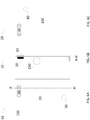
- FIG. 1A illustrates a plan view of a front face in a portable electronic device 10, according to some embodiments.
- Portable electronic device 10 includes a housing 150 holding a display cover 20 and having a sensor aperture 30. Sensor aperture 30 may Portable electronic device 10 also includes at least an RF antenna 50 which may be integrated into housing 150.
- RF antenna 50 may be in the interior side of housing 150.
- portable electronic device 10 may include multiple RF antennas, some of which may be integrated into housing 150, and others may be included in the interior side of housing 150. While RF antenna 50 in FIG. 1A is shown as a coil wrapping around display cover 20, other configurations are possible.
- Housing 150 may include an RF-transparent layer 100 over a hard material substrate 110.
- RF-transparent layer 100 may be an oxide layer formed from hard material substrate 110.
- hard material layer 110 may include an aluminum layer and RF-transparent layer 100 may be aluminum oxide formed from converting a portion of the aluminum layer.
- RF-transparent layer may be an exterior layer of housing 150, and hard material layer 110 may be an interior layer of housing 150.
- FIG. 1B illustrates a cross-sectional view of portable electronic device 10, according to some embodiments.
- the cross-section in FIG. 1B is taken along segment A-A' (cf. FIG. 1A).
- FIG. 1B illustrates a configuration where RF antenna 50 is integrated into housing 150. While RF antenna 50 includes a conductive portion, the antenna is configured to include portions of RF-transparent layer 120 separating different segments of RF antenna 50.
- hard material substrate 110 includes a metal. Thus, hard material layer 110 provides structural support to the electronic device, and also a ground connection for RF antenna 50, in some embodiments.
- RF-transparent layer 100 may include an electrically resistive material (e.g., aluminum oxide) effectively isolating segments of RF antenna 50 from each other and from other conductive portions of housing 150 (e.g., aluminum layer 110).
- FIG. 1C illustrates a plan view of a back face in portable electronic device 10, according to some embodiments. Accordingly, in some embodiments a cross section of housing 150 as shown in FIG. 1B may include no conductive material, such as aluminum (e.g., layer 110) in certain portions of housing 150 (e.g., layers 120). Such embodiments enable antenna 50 to be integrated within housing 150 as the non-conductive material in layer 120 is adjacent to the conductive path in antenna 50.
- an electrically resistive material e.g., aluminum oxide
- FIG. 1C illustrates a sensor aperture 40 which may be configured to allow a camera to receive visible light from outside of housing 150.
- aperture 40 may be configured to allow an audio device to transmit or receive acoustic signals to and from outside housing 150.
- FIGS. 2A-2C illustrate steps in a method of forming housing 150 for electronic device 10 including Radio-Frequency (RF) antenna 50 according to some embodiments.
- FIG. 2A illustrates a step of placing a non-conductive material 211 in a hard material layer 201 forming housing 150.
- Hard material layer 201 may include an electrically conductive material such as a metal (e.g., aluminum).
- Non-conductive material 211 may be a plastic, a ceramic material, or glass.
- non-conductive material 211 may include a thermosetting polymer, an epoxy, or some other glue including a curable resin.
- the step illustrated in FIG. 2A may include forming a gap in hard material layer 201 and molding plastic material 211 inside the gap.
- the gap may have the profile of an antenna window, and be formed in a portion of housing 150 proximate or adjacent to RF antenna 50.
- FIG. 2B illustrates a step of coating a thin layer of hard material 205 on a side of housing 150 overlapping layers 201 and non-conductive material 211.
- Layer 205 may include the same material as layer 201.
- layer 201 is aluminum
- layer 205 may be formed by coating a thin aluminum layer on the side of housing 150, as illustrated in FIG. 2B .
- the step in FIG. 2B may include Physical Vapor Deposition (PVD) of a metal to form layer 205. Examples of PVD may include sputtering and other procedures known in the art. Accordingly, the step in FIG.
- PVD Physical Vapor Deposition
- FIG. 2B may include metallization of a ceramics substrate by steps including ion vapor deposition, chemical vapor deposition (CVD), cathodic arc deposition, plasma spray, and others known in the art.
- FIG. 2C illustrates a step of oxidizing the thin layer of hard material 205 to form a thin RF-transparent layer 221.
- thin RF-transparent layer 211 includes an aluminum oxide layer formed by anodization of thin aluminum layer 205.
- RF-transparent layer 211 can include metal, just not solid bulk metal or alloy that will block RF transmission. As a result of the steps illustrates in FIGS.
- FIGS. 3A-3C illustrate steps in a method of forming housing 150 for electronic device 10 including antenna 50, according to some embodiments.
- FIG. 3A illustrates a step providing a layer of hard material 201 (cf. FIGS. 2A-2C , above).
- FIG. 3B illustrates a step of forming RF-transparent layer 221 adjacent to layer 201 (cf. FIG. 2C ). Accordingly, the step in FIG. 3B may include anodizing an aluminum layer 201 to form aluminum oxide layer 221 with a pre-selected thickness.
- the thickness of aluminum oxide layer 221 may be about 12 ⁇ m. Such an aluminum oxide layer may result from 'consuming' an approximately 5 ⁇ m to 6 ⁇ m aluminum layer through anodization.
- FIG. 3C illustrates a step of forming a non-conductive layer 231 in a portion of hard material layer 201. The step in FIG. 3C may include a 'hard' anodization process to form a thick aluminum oxide layer 231 having a similar thickness as hard material layer 201. For example, in embodiments where hard material layer 201 includes aluminum, the step in FIG.
- 3C may include using Plasma Electrolytic Oxidation (PEO) to produce a thick layer of alumina (aluminum oxide in crystalline form), also known as sapphire, as non-conductive layer 231.
- the step in FIG. 3C may include use of a mask overlapping portions of hard material layer 201 so that layer 231 separates portions of hard material layer 201, prior to anodizing layer 201.
- layer 231 may be thicker than layer 221.
- layer 231 may be up to 50 ⁇ m thick, or even more.
- Some embodiments consistent with the present disclosure may form a thinner aluminum oxide layer 221 on the exterior portion of housing 150, and a thicker aluminum oxide layer 231 on the interior portion of housing 150.
- a thinner aluminum oxide layer 221 may be as layer 100 covering all or almost all of the exterior side of housing 150, and a thicker aluminum oxide layer 231 may cover selected portions of the interior side of housing 150 (e.g., layer 120, cf. FIGS. 1A-1C ).
- FIG. 4A illustrates a partial plan view of a housing 450 for electronic device 10 including RF antenna 50, according to some embodiments.
- Housing 450 may include a honeycomb configuration where islands 451 made of hard material 201 are isolated from one another by channels 421.
- Islands 451 may include a conductive material such as aluminum, and channels 421 may include a non-conductive material (e.g., non-conductive material 211, cf. FIG. 2C ).
- FIG. 4A illustrates a honeycomb structure having similar hexagonally shaped islands 451 adjacent to one another.
- the honeycomb structure can provide stiffness to RF antenna 50 and can provide areas that are sufficiently thin so as to be fully anodized to RF transparent material. While this is an exemplary embodiment, one of ordinary skill would recognize that islands 451 may have any shape. Furthermore, islands 451 may have different shape and size from one another.
- FIGS. 4B-D illustrate steps in a method of forming housing 450 for electronic device 10 including RF antenna 50 according to some embodiments.
- FIG. 4B illustrates a step of forming micro perforations 420 in a hard material layer 201 (cf. FIGS. 2A-2C and FIGS. 3A-3C ).
- Micro perforations 420 can be used to reduce the thickness of hard material layer 201 in areas of micro perforations 420 while maintaining its stiffness.
- the micro perforations 420 goes through the aluminum and through an aluminum oxide layer adjacent to the aluminum.
- Micro perforations 420 may be formed by laser machining of aluminum in hard material layer 201.
- the step in FIG. 4C may include selectively anodizing the aluminum in hard material layer 201 to form areas of aluminum oxide, which are RF transparent.
- anodizing forms an aluminum oxide layer having a thickness of between about 5 to 300 microns.
- aluminum oxide can be formed at micro perforations 420 where the aluminum is very thin. Since the aluminum is thin at micro perforations 420, these regions can have cross sections that are fully anodized to aluminum oxide, thereby creating areas within RF antenna 50 that are RF transparent.
- the step in FIG. 4C may include using a mask to cover a portion 461 of hard material 201.
- Portion 461 may form an island of aluminum, a metal, or some other conducting material surrounded by non-conductive layer 231.
- FIG. 4D illustrates a step of forming a support layer 471 on a side of housing 150.
- Support layer 471 provides structural integrity and stiffness to housing 150.
- support layer 471 may include a fiberglass coating, or a thin layer of glass or plastic. It is desirable that support layer 471 be made of a non-conducting material so as not to compromise the operation of an RF antenna integrated in housing 150.
- FIG. 4D also illustrates portions 421 and 451 of housing 450 (cf. FIG. 4A ).
- FIGS. 5A-5B illustrate steps in a method of forming housing 450 for electronic device 10 including RF antenna 50, according to some embodiments.
- FIG. 5A illustrates a step similar to the step illustrated in FIG. 4B .
- FIG. 5B illustrates a step of forming a non-conductive layer 231 from portions of hard material layer 201, and forming an RF-transparent layer 221 on a side of housing 150, overlapping non-conductive layer 231 and portion 461.
- FIGS. 6A-6C illustrate a portable electronic device 10 including an antenna window 60.
- FIG. 6A illustrates a plan view of a front face in portable electronic device 10 including antenna window 60.
- FIG. 6A includes display cover 20 and sensor aperture 30, as described in detail above (cf. FIG. 1A ).
- FIG. 6B illustrates a cross-sectional view of portable electronic device 10 including antenna window 60.
- Antenna window 60 is placed in apportion of housing 150 proximal to RF antenna 50.
- Antenna window 60 may be adjacent to RF antenna 50.
- FIG. 6C illustrates a plan view of a back face in portable electronic device 10 including antenna window 60.
- FIG. 6C also includes sensor aperture 40, as described in detail above (cf. FIG. 1C ).
- embodiments consistent with the present disclosure may include multiple RF antennas located in different areas in portable electronic device 10.
- an RF antenna may be integrated in housing 150 (cf. FIG. 1A ), and another RF-antenna may be in the interior side of housing 150, adjacent to antenna window 60 (cf. FIG. 6B ).
- FIGS. 7A-7D illustrate steps in a method of forming housing 150 for electronic device 10 including RF antenna 50, according to some embodiments.
- FIG. 7A illustrates a step of forming an RF-transparent layer 221 adjacent to a hard material layer 201.
- the geometry of the cavity can be in the form of a pocket, trench, or any suitable shape that does not break the plane of layer 221.
- FIG. 7B illustrates a step of forming a cavity in hard material layer 201.
- the step in FIG. 7B may include machining the cavity, or etching away a portion of material in layer 201 to form the cavity.
- FIG. 7C illustrates a step of removing a thin residual of material in layer 201 adjacent to layer 221 in the cavity.
- the cavity can be formed by laser ablation, chemical etch, or other suitable technique as recognized by a person of skill in the art.
- FIG. 7D illustrates a step of filling the cavity in layer 201 with non-conductive material 211.
- FIGS. 8A-8G illustrate steps in a method of forming housing 150 for electronic device 10 including RF antenna 60, according to some embodiments.
- FIG. 8A illustrates a step similar to the step illustrated in FIG. 7A .
- FIG. 8B illustrates a step similar to step 7B illustrated in FIG. 7B .
- FIG. 8C illustrates a step of forming a masking layer 801 around layers 201 and 221, including the cavity formed in the step illustrated in FIG. 8B.
- FIG. 8D illustrates a step of selectively removing masking layer 801 in an area overlapping a residual thickness of material 201 adjacent to layer 221 in the cavity formed in the step illustrated in FIG. 8B .
- FIG. 8D may include etching away masking layer 801 in the selected portion.
- FIG. 8E illustrates a step of removing the hard material 201 left unmasked in step 8D.
- FIG. 8F illustrates a step of removing residual masking layer 801.
- FIG. 8G illustrates a step of filling the cavity with non-conductive material 211.
- an RF-antenna window may include removing all aluminum material in the window area (cf. FIG. 7D and 8E ). Such configuration enhances the RF-transparency of the window, as aluminum layers of even a few nm thick have a non-zero absorbance in the RF frequency spectrum.
- FIG. 9 illustrates a cross-sectional view of housing 150 for electronic device 10 including RF antenna 50, according to some embodiments. Accordingly, FIG. 9 illustrates hard material layer 201, RF-transparent layer 221, and non-conductive layer 211 in a gap of layer 201. Non-conductive layer 211 includes RF antenna 50. In some embodiments, RF antenna 50 includes a strip of conductive material (e.g., aluminum) adjacent to RF-transparent layer 221.
- conductive material e.g., aluminum
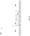
- FIG. 10 illustrates a cross-sectional view of housing 150 for electronic device 10 including RF antenna 50, according to some embodiments. Accordingly, FIG. 10 illustrates hard material layer 201, RF-transparent layer 221, and non-conductive layer 211 in a gap of layer 201. Non-conductive layer 211 includes RF antenna 50. In some embodiments, RF antenna 50 includes a strip of conductive material (e.g., aluminum) embedded within non-conductive layer 211.
- conductive material e.g., aluminum
- FIG. 11A-11B illustrate steps in a method of forming housing 150 for electronic device 10 including RF antenna 50 according to some embodiments.
- FIG. 11A illustrates a step of forming a gap in a hard material layer 201. The step in FIG. 11A also includes placing a block including RF-transparent layer 221 adjacent to non-conductive layer 211 in the gap formed in layer 201.
- FIG. 11B illustrates a step of extending RF-transparent layer 221 across the gap, overlapping hard material layer 201.
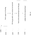
- FIG. 12 illustrates a flow chart with steps in a method 1200 of forming housing 150 for electronic device 10 including RF antenna 50 according to some embodiments.
- Step 1210 includes forming a gap on the housing.
- the housing may include a hard material layer made of aluminum (e.g., layer 110, cf. FIG. 1B ). Accordingly, step 1210 may be as described in detail in relation to FIG. 2A .
- Step 1220 includes filling the gap with a non-conductive material. Accordingly, steps 1210 and 1220 may be included in the steps illustrated in detail in relation to FIG. 2A .
- Step 1230 includes forming a thin material layer over the gap (cf. FIG. 2B ).
- step 1240 includes oxidizing the thin material layer (cf. FIG. 2C ). Accordingly, step 1240 may include forming an RF-transparent layer adjacent to a portion of the hard material layer and the non-conductive material filling the gap in the hard material layer.
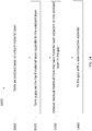
- FIG. 13 illustrates a flow chart with steps in a method 1300 of forming housing 150 for electronic device 10 including RF antenna 50, according to some embodiments.
- Step 1310 includes forming a first oxidized layer on a first side of a hard material layer.
- step 1310 may include anodizing an aluminum layer to form a thin RF-transparent layer on one side (e.g., layer 221, cf. FIG. 3B ).
- Step 1320 includes forming a second oxidized layer on a second side of the hard material layer (e.g., layer 231, cf. FIG. 3C ).
- FIG. 14 illustrates a flow chart with steps in a method 1400 of forming housing 150 for electronic device 10 including RF antenna 50, according to some embodiments.
- Step 1410 includes forming an oxidized layer on a hard material layer.
- step 1410 may include anodizing an aluminum layer to form a thin RF-transparent layer (e.g., layer 221, cf. FIGS. 7A and 8A ).
- Step 1420 includes forming a gap on the hard material layer on a side opposite to the oxidized layer (cf. FIGS. 7B and 8B ).
- Step 1430 includes removing residual material from the hard material layer adjacent to the oxidized layer in the gap (cf. FIGS. 7C and 8C-F ).
- Step 1440 includes filling the gap with a non-conductive material (cf. FIGS. 7D and 8G ).
- patch 60 may include a touch sensitive pad configured to receive a touch from the user.
- the touch sensitive pad may be capacitively coupled to an electronic circuit configured to determine touch position and gesture interpretation.
Landscapes
- Chemical & Material Sciences (AREA)
- Engineering & Computer Science (AREA)
- Chemical Kinetics & Catalysis (AREA)
- Materials Engineering (AREA)
- Mechanical Engineering (AREA)
- Metallurgy (AREA)
- Organic Chemistry (AREA)
- Inorganic Chemistry (AREA)
- Computer Networks & Wireless Communication (AREA)
- General Chemical & Material Sciences (AREA)
- Support Of Aerials (AREA)
- Telephone Set Structure (AREA)
Description
- The described embodiments relate generally to housings for electronic devices adapted to include radio-frequency (RF) antennas. More particularly, embodiments disclosed herein relate to metallic housings for portable electronic devices adapted to include radio-frequency antennas.
- Antenna architecture is an integral part of a consumer electronics product. Housings and structural components are often made from conductive metal, which can serve as a ground for an antenna. However, antennas require nonconductive regions or other isolation to provide a good radiation pattern and signal strength. To solve this problem conventional designs include a plastic antenna window or a plastic split in a housing to separate the conductive metal. However, this approach breaks the consistent visual profile of the device, deteriorating the cosmetic appeal of the metal surface. Also, replacing metallic portions of the housing with softer materials weakens the underlying metal and uses device volume to fasten the parts together.
- Therefore, what is desired is a housing for an electronic device that integrates antenna designs in a manner that is visually consistent with the cosmetic appeal of the device and that provides structural support for the device and functional support for the antenna.
A thermal spray coating for a seamless and radio-transparent electronic device housing is described inUS 2010/0103612 . Here, a ceramic coating is adapted to allow communications to/from an internal antenna via electromagnetic waves.
US 2013/0008796 describes anodized electroplated aluminum structures and methods for making the same. Here, cosmetic structures are provided by electroplating a non-cosmetic structure with aluminum and then anodizing the electroplated aluminum. A display apparatus and mobile terminal is described inWO 2009/014366 . Here, a display apparatus comprising a loop antenna portion for wireless communication is provided.
US 2012/0146857 describes an antenna module, a touch module and an electronic device. Here, the antenna module includes a transparent substrate and an antenna circuit disposed on the transparent substitute. - The present invention relates to a housing for an electronic device as defined by claims 1-5 and to a method for manufacturing said housing as defined by claims 6-11.
- In a first embodiment, a housing for an electronic device is provided. The housing includes a metal layer including a radio-frequency (RF) antenna. The housing further includes a first and second gap formed through a thickness of the metal layer and arranged to form an electrically isolated segment of the metal layer configured to function as an RF antenna. The housing further includes a non-conductive material filling the first and second gaps in the metal layer and a metal oxide layer formed on an exterior surface of the metal layer and extending across the first and the second gaps and the electrically isolated segment, wherein metal oxide layer forms an RF-transparent window to allow transmission of RF radiation through the window.
- In another embodiment, a method of manufacturing a housing for an electronic device is provided. The method may include converting an aluminum layer in the housing to an exterior aluminum oxide layer. The method may also include removing the aluminum layer adjacent to the aluminum oxide layer to form a gap in a window portion of the housing. The method additionally includes filling the gap in the window portion with a non-conductive material. Accordingly, the gap allows transmission of substantially all RF radiation through the window portion.
- Other aspects and advantages of the invention will become apparent from the following detailed description taken in conjunction with the accompanying drawings which illustrate, by way of example, the principles of the described embodiments.
- The described embodiments may be better understood by reference to the following description and the accompanying drawings. Additionally, advantages of the described embodiments may be better understood by reference to the following description and accompanying drawings. These drawings do not limit any changes in form and detail that may be made to the described embodiments.
-
FIGS. 1A-1C illustrate a portable electronic device according to some embodiments. -
FIGS. 2A-2C illustrate steps in a method of forming a housing for an electronic device including a Radio-Frequency (RF) antenna according to some embodiments. -
FIGS. 3A-3C illustrate steps in a method of forming a housing for an electronic device including an RF antenna, according to some embodiments. -
FIG. 4A illustrates a partial plan view of a housing for an electronic device including an RF antenna, according to some embodiments. -
FIGS. 4B-4D illustrate steps in a method of forming a housing for an electronic device including an RF antenna according to some embodiments. -
FIGS. 5A-5B illustrate steps in a method of forming a housing for an electronic device including an RF antenna according to some embodiments. -
FIGS. 6A-6C illustrate a portable electronic device. -
FIGS. 7A-7D illustrate steps in a method of forming a housing for an electronic device including an RF antenna according to some embodiments. -
FIGS. 8A-8G illustrate steps in a method of forming a housing for an electronic device including an RF antenna according to some embodiments. -
FIG. 9 illustrates a cross-sectional view of a housing for an electronic device including an RF antenna, according to some embodiments. -
FIG. 10 illustrates a cross-sectional view of a housing for an electronic device including an RF antenna, according to some embodiments. -
FIG. 11A-11B illustrate steps in a method of forming a housing for an electronic device including an RF antenna according to some embodiments. -
FIG. 12 illustrates a flow chart with steps in a method of forming a housing for an electronic device including an RF antenna according to some embodiments. -
FIG. 13 illustrates a flow chart with steps in a method of forming a housing for an electronic device including an RF antenna, according to some embodiments. -
FIG. 14 illustrates a flow chart with steps in a method of forming a housing for an electronic device including an RF antenna, according to some embodiments. - In the figures, elements referred to with the same or similar reference numerals include the same or similar structure, use, or procedure, as described in the first instance of occurrence of the reference numeral.
- The various aspects, embodiments, implementations or features of the described embodiments can be used separately or in any combination. Various aspects of the described embodiments can be implemented by software, hardware or a combination of hardware and software. The described embodiments can also be embodied as computer readable code on a computer readable medium for controlling manufacturing operations or as computer readable code on a computer readable medium for controlling a manufacturing line. The computer readable medium is any data storage device that can store data, which can thereafter be read by a computer system. Examples of the computer readable medium include read-only memory, random-access memory, CD-ROMs, HDDs, DVDs, magnetic tape, and optical data storage devices. The computer readable medium can also be distributed over network-coupled computer systems so that the computer readable code is stored and executed in a distributed fashion.
- Electronic device housings consistent with the present disclosure include a hard, cosmetic anodized surface of aluminum. The anodized surface is nonconductive and thus is transparent to radio-frequency (RF) electronic radiation. In some embodiments, the anodized surface may have a thickness on the order of 10 microns (1 micron = 1 µm = 10-6 m). By adjusting the anodization parameters the anodization depth can be made to have a thickness of over 100 microns. A number of design techniques (outlined in the attachment) can be used to create a continuous, anodized, cosmetic aluminum surface that is selectively conductive in certain portions and non-conductive in other portions. This allows an antenna window or even an antenna to be patterned directly into the housing. Such electronic device housing improves product cosmetics, and reduces the size of the device.
- Antenna windows in aluminum enclosures are challenging. Prior solutions include splits in housings and plastic covered antenna windows. Our proposed solution is to use aluminum oxide as the antenna window. Aluminum oxide is non-conductive and transparent to RF. Aluminum oxide is created during the process of anodization. The thickness can be nominally up to 100 um thick or higher by careful adjustment of the anodization parameters. The process, as outlined in the attached, includes anodization of the exterior housing and then etching away on the interior of the housing antenna windows at desired locations for antenna windows, followed by filling in the etched portions with plastic, paint, or other suitable material to maintain structural integrity. The aluminum oxide can be substantially clear or transparent, allowing the filling material to show through. The resulting housing is cosmetically pleasing and without cracks or apparent plastic portions.
- Accordingly, embodiments consistent with the present disclosure provide a housing for an electronic device integrating antenna designs in a manner that is visually consistent with the cosmetic appeal of the device. In some embodiments, an electronic device housing provides structural support for the device and functional support for the antenna integrated in the device. In some embodiments, a housing for an electronic device includes a window for an antenna, the window providing RF-transparency for the antenna signals while maintaining a consistent visual appeal for the device. Also, the RF-transparent window maintains a structural support for the housing.
-
FIG. 1A illustrates a plan view of a front face in a portableelectronic device 10, according to some embodiments. Portableelectronic device 10 includes ahousing 150 holding adisplay cover 20 and having asensor aperture 30.Sensor aperture 30 may Portableelectronic device 10 also includes at least anRF antenna 50 which may be integrated intohousing 150. In someembodiments RF antenna 50 may be in the interior side ofhousing 150. In that regard, portableelectronic device 10 may include multiple RF antennas, some of which may be integrated intohousing 150, and others may be included in the interior side ofhousing 150. WhileRF antenna 50 inFIG. 1A is shown as a coil wrapping arounddisplay cover 20, other configurations are possible.Housing 150 may include an RF-transparent layer 100 over ahard material substrate 110. In some embodiments, RF-transparent layer 100 may be an oxide layer formed fromhard material substrate 110. For example,hard material layer 110 may include an aluminum layer and RF-transparent layer 100 may be aluminum oxide formed from converting a portion of the aluminum layer. Accordingly, RF-transparent layer may be an exterior layer ofhousing 150, andhard material layer 110 may be an interior layer ofhousing 150. -
FIG. 1B illustrates a cross-sectional view of portableelectronic device 10, according to some embodiments. The cross-section inFIG. 1B is taken along segment A-A' (cf.FIG. 1A). FIG. 1B illustrates a configuration whereRF antenna 50 is integrated intohousing 150. WhileRF antenna 50 includes a conductive portion, the antenna is configured to include portions of RF-transparent layer 120 separating different segments ofRF antenna 50. As mentioned above, in some embodiments hardmaterial substrate 110 includes a metal. Thus,hard material layer 110 provides structural support to the electronic device, and also a ground connection forRF antenna 50, in some embodiments. RF-transparent layer 100 may include an electrically resistive material (e.g., aluminum oxide) effectively isolating segments ofRF antenna 50 from each other and from other conductive portions of housing 150 (e.g., aluminum layer 110).FIG. 1C illustrates a plan view of a back face in portableelectronic device 10, according to some embodiments. Accordingly, in some embodiments a cross section ofhousing 150 as shown inFIG. 1B may include no conductive material, such as aluminum (e.g., layer 110) in certain portions of housing 150 (e.g., layers 120). Such embodiments enableantenna 50 to be integrated withinhousing 150 as the non-conductive material inlayer 120 is adjacent to the conductive path inantenna 50. The non-conductive material inlayer 120 electrically insulates a first segment inantenna 50 from a second segment in the conductive path ofantenna 50.FIG. 1C illustrates asensor aperture 40 which may be configured to allow a camera to receive visible light from outside ofhousing 150. In someembodiments aperture 40 may be configured to allow an audio device to transmit or receive acoustic signals to and fromoutside housing 150. -
FIGS. 2A-2C illustrate steps in a method of forminghousing 150 forelectronic device 10 including Radio-Frequency (RF)antenna 50 according to some embodiments.FIG. 2A illustrates a step of placing anon-conductive material 211 in ahard material layer 201 forminghousing 150.Hard material layer 201 may include an electrically conductive material such as a metal (e.g., aluminum).Non-conductive material 211 may be a plastic, a ceramic material, or glass. In some embodiments,non-conductive material 211 may include a thermosetting polymer, an epoxy, or some other glue including a curable resin. The step illustrated inFIG. 2A may include forming a gap inhard material layer 201 andmolding plastic material 211 inside the gap. Accordingly, the gap may have the profile of an antenna window, and be formed in a portion ofhousing 150 proximate or adjacent toRF antenna 50.FIG. 2B illustrates a step of coating a thin layer ofhard material 205 on a side ofhousing 150 overlappinglayers 201 andnon-conductive material 211.Layer 205 may include the same material aslayer 201. For example, iflayer 201 is aluminum,layer 205 may be formed by coating a thin aluminum layer on the side ofhousing 150, as illustrated inFIG. 2B . The step inFIG. 2B may include Physical Vapor Deposition (PVD) of a metal to formlayer 205. Examples of PVD may include sputtering and other procedures known in the art. Accordingly, the step inFIG. 2B may include metallization of a ceramics substrate by steps including ion vapor deposition, chemical vapor deposition (CVD), cathodic arc deposition, plasma spray, and others known in the art.FIG. 2C illustrates a step of oxidizing the thin layer ofhard material 205 to form a thin RF-transparent layer 221. In some embodiments, thin RF-transparent layer 211 includes an aluminum oxide layer formed by anodization ofthin aluminum layer 205. RF-transparent layer 211 can include metal, just not solid bulk metal or alloy that will block RF transmission. As a result of the steps illustrates inFIGS. 2A-2C , a portion ofhousing 150 has a cross-section such that an RF-transparent path is formed from an exterior side ofhousing 150 to an interior side ofhousing 150.
FIGS. 3A-3C illustrate steps in a method of forminghousing 150 forelectronic device 10 includingantenna 50, according to some embodiments.FIG. 3A illustrates a step providing a layer of hard material 201 (cf.FIGS. 2A-2C , above).FIG. 3B illustrates a step of forming RF-transparent layer 221 adjacent to layer 201 (cf.FIG. 2C ). Accordingly, the step inFIG. 3B may include anodizing analuminum layer 201 to formaluminum oxide layer 221 with a pre-selected thickness. In some embodiments, the thickness ofaluminum oxide layer 221 may be about 12 µm. Such an aluminum oxide layer may result from 'consuming' an approximately 5 µm to 6 µm aluminum layer through anodization.FIG. 3C illustrates a step of forming anon-conductive layer 231 in a portion ofhard material layer 201. The step inFIG. 3C may include a 'hard' anodization process to form a thickaluminum oxide layer 231 having a similar thickness ashard material layer 201. For example, in embodiments wherehard material layer 201 includes aluminum, the step inFIG. 3C may include using Plasma Electrolytic Oxidation (PEO) to produce a thick layer of alumina (aluminum oxide in crystalline form), also known as sapphire, asnon-conductive layer 231. In some embodiments, the step inFIG. 3C may include use of a mask overlapping portions ofhard material layer 201 so thatlayer 231 separates portions ofhard material layer 201, prior toanodizing layer 201. Accordingly,layer 231 may be thicker thanlayer 221. In some embodiments,layer 231 may be up to 50 µm thick, or even more. Some embodiments consistent with the present disclosure may form a thinneraluminum oxide layer 221 on the exterior portion ofhousing 150, and a thickeraluminum oxide layer 231 on the interior portion ofhousing 150. Thus, a thinneraluminum oxide layer 221 may be aslayer 100 covering all or almost all of the exterior side ofhousing 150, and a thickeraluminum oxide layer 231 may cover selected portions of the interior side of housing 150 (e.g.,layer 120, cf.FIGS. 1A-1C ). -
FIG. 4A illustrates a partial plan view of ahousing 450 forelectronic device 10 includingRF antenna 50, according to some embodiments.Housing 450 may include a honeycomb configuration whereislands 451 made ofhard material 201 are isolated from one another bychannels 421.Islands 451 may include a conductive material such as aluminum, andchannels 421 may include a non-conductive material (e.g.,non-conductive material 211, cf.FIG. 2C ).FIG. 4A illustrates a honeycomb structure having similar hexagonally shapedislands 451 adjacent to one another. The honeycomb structure can provide stiffness toRF antenna 50 and can provide areas that are sufficiently thin so as to be fully anodized to RF transparent material. While this is an exemplary embodiment, one of ordinary skill would recognize thatislands 451 may have any shape. Furthermore,islands 451 may have different shape and size from one another. -
FIGS. 4B-D illustrate steps in a method of forminghousing 450 forelectronic device 10 includingRF antenna 50 according to some embodiments.FIG. 4B illustrates a step of formingmicro perforations 420 in a hard material layer 201 (cf.FIGS. 2A-2C andFIGS. 3A-3C ).Micro perforations 420 can be used to reduce the thickness ofhard material layer 201 in areas ofmicro perforations 420 while maintaining its stiffness. In embodiments wherehard material layer 201 includes aluminum, themicro perforations 420 goes through the aluminum and through an aluminum oxide layer adjacent to the aluminum.Micro perforations 420 may be formed by laser machining of aluminum inhard material layer 201.FIG. 4C illustrates a step of formingnon-conductive layer 231 from portions ofhard material layer 201. Accordingly, the step inFIG. 4C may include selectively anodizing the aluminum inhard material layer 201 to form areas of aluminum oxide, which are RF transparent. In some embodiments, anodizing forms an aluminum oxide layer having a thickness of between about 5 to 300 microns. In particular, aluminum oxide can be formed atmicro perforations 420 where the aluminum is very thin. Since the aluminum is thin atmicro perforations 420, these regions can have cross sections that are fully anodized to aluminum oxide, thereby creating areas withinRF antenna 50 that are RF transparent. The step inFIG. 4C may include using a mask to cover aportion 461 ofhard material 201.Portion 461 may form an island of aluminum, a metal, or some other conducting material surrounded bynon-conductive layer 231.FIG. 4D illustrates a step of forming asupport layer 471 on a side ofhousing 150.Support layer 471 provides structural integrity and stiffness tohousing 150. In some embodiments,support layer 471 may include a fiberglass coating, or a thin layer of glass or plastic. It is desirable thatsupport layer 471 be made of a non-conducting material so as not to compromise the operation of an RF antenna integrated inhousing 150.FIG. 4D also illustratesportions FIG. 4A ). -
FIGS. 5A-5B illustrate steps in a method of forminghousing 450 forelectronic device 10 includingRF antenna 50, according to some embodiments.FIG. 5A illustrates a step similar to the step illustrated inFIG. 4B .FIG. 5B illustrates a step of forming anon-conductive layer 231 from portions ofhard material layer 201, and forming an RF-transparent layer 221 on a side ofhousing 150, overlappingnon-conductive layer 231 andportion 461. -
FIGS. 6A-6C illustrate a portableelectronic device 10 including anantenna window 60.FIG. 6A illustrates a plan view of a front face in portableelectronic device 10 includingantenna window 60.FIG. 6A includesdisplay cover 20 andsensor aperture 30, as described in detail above (cf.FIG. 1A ).FIG. 6B illustrates a cross-sectional view of portableelectronic device 10 includingantenna window 60.Antenna window 60 is placed in apportion ofhousing 150 proximal toRF antenna 50.Antenna window 60 may be adjacent toRF antenna 50.FIG. 6C illustrates a plan view of a back face in portableelectronic device 10 includingantenna window 60.FIG. 6C also includessensor aperture 40, as described in detail above (cf.FIG. 1C ). As mentioned above in reference toFIGS. 1A-1C , embodiments consistent with the present disclosure may include multiple RF antennas located in different areas in portableelectronic device 10. For example, an RF antenna may be integrated in housing 150 (cf.FIG. 1A ), and another RF-antenna may be in the interior side ofhousing 150, adjacent to antenna window 60 (cf.FIG. 6B ). -
FIGS. 7A-7D illustrate steps in a method of forminghousing 150 forelectronic device 10 includingRF antenna 50, according to some embodiments.FIG. 7A illustrates a step of forming an RF-transparent layer 221 adjacent to ahard material layer 201. The geometry of the cavity can be in the form of a pocket, trench, or any suitable shape that does not break the plane oflayer 221.FIG. 7B illustrates a step of forming a cavity inhard material layer 201. The step inFIG. 7B may include machining the cavity, or etching away a portion of material inlayer 201 to form the cavity.FIG. 7C illustrates a step of removing a thin residual of material inlayer 201 adjacent to layer 221 in the cavity. The cavity can be formed by laser ablation, chemical etch, or other suitable technique as recognized by a person of skill in the art.FIG. 7D illustrates a step of filling the cavity inlayer 201 withnon-conductive material 211. -
FIGS. 8A-8G illustrate steps in a method of forminghousing 150 forelectronic device 10 includingRF antenna 60, according to some embodiments.FIG. 8A illustrates a step similar to the step illustrated inFIG. 7A .FIG. 8B illustrates a step similar to step 7B illustrated inFIG. 7B .FIG. 8C illustrates a step of forming amasking layer 801 aroundlayers FIG. 8B. FIG. 8D illustrates a step of selectively removingmasking layer 801 in an area overlapping a residual thickness ofmaterial 201 adjacent to layer 221 in the cavity formed in the step illustrated inFIG. 8B . The step illustrated inFIG. 8D may include etching away maskinglayer 801 in the selected portion.FIG. 8E illustrates a step of removing thehard material 201 left unmasked in step 8D.FIG. 8F illustrates a step of removingresidual masking layer 801.FIG. 8G illustrates a step of filling the cavity withnon-conductive material 211. - Accordingly, in embodiments of
housing 150 forelectronic device 10 where thehard material layer 110 forming the housing is aluminum, some embodiments of an RF-antenna window may include removing all aluminum material in the window area (cf.FIG. 7D and8E ). Such configuration enhances the RF-transparency of the window, as aluminum layers of even a few nm thick have a non-zero absorbance in the RF frequency spectrum. -
FIG. 9 illustrates a cross-sectional view ofhousing 150 forelectronic device 10 includingRF antenna 50, according to some embodiments. Accordingly,FIG. 9 illustrateshard material layer 201, RF-transparent layer 221, andnon-conductive layer 211 in a gap oflayer 201.Non-conductive layer 211 includesRF antenna 50. In some embodiments,RF antenna 50 includes a strip of conductive material (e.g., aluminum) adjacent to RF-transparent layer 221. -
FIG. 10 illustrates a cross-sectional view ofhousing 150 forelectronic device 10 includingRF antenna 50, according to some embodiments. Accordingly,FIG. 10 illustrateshard material layer 201, RF-transparent layer 221, andnon-conductive layer 211 in a gap oflayer 201.Non-conductive layer 211 includesRF antenna 50. In some embodiments,RF antenna 50 includes a strip of conductive material (e.g., aluminum) embedded withinnon-conductive layer 211. -
FIG. 11A-11B illustrate steps in a method of forminghousing 150 forelectronic device 10 includingRF antenna 50 according to some embodiments.FIG. 11A illustrates a step of forming a gap in ahard material layer 201. The step inFIG. 11A also includes placing a block including RF-transparent layer 221 adjacent tonon-conductive layer 211 in the gap formed inlayer 201.FIG. 11B illustrates a step of extending RF-transparent layer 221 across the gap, overlapping hardmaterial layer 201. -
FIG. 12 illustrates a flow chart with steps in amethod 1200 of forminghousing 150 forelectronic device 10 includingRF antenna 50 according to some embodiments.Step 1210 includes forming a gap on the housing. The housing may include a hard material layer made of aluminum (e.g.,layer 110, cf.FIG. 1B ). Accordingly,step 1210 may be as described in detail in relation toFIG. 2A .Step 1220 includes filling the gap with a non-conductive material. Accordingly, steps 1210 and 1220 may be included in the steps illustrated in detail in relation toFIG. 2A .Step 1230 includes forming a thin material layer over the gap (cf.FIG. 2B ). And step 1240 includes oxidizing the thin material layer (cf.FIG. 2C ). Accordingly,step 1240 may include forming an RF-transparent layer adjacent to a portion of the hard material layer and the non-conductive material filling the gap in the hard material layer. -
FIG. 13 illustrates a flow chart with steps in amethod 1300 of forminghousing 150 forelectronic device 10 includingRF antenna 50, according to some embodiments.Step 1310 includes forming a first oxidized layer on a first side of a hard material layer. In some embodiments,step 1310 may include anodizing an aluminum layer to form a thin RF-transparent layer on one side (e.g.,layer 221, cf.FIG. 3B ).Step 1320 includes forming a second oxidized layer on a second side of the hard material layer (e.g.,layer 231, cf.FIG. 3C ). -
FIG. 14 illustrates a flow chart with steps in amethod 1400 of forminghousing 150 forelectronic device 10 includingRF antenna 50, according to some embodiments.Step 1410 includes forming an oxidized layer on a hard material layer. In some embodiments,step 1410 may include anodizing an aluminum layer to form a thin RF-transparent layer (e.g.,layer 221, cf.FIGS. 7A and8A ).Step 1420 includes forming a gap on the hard material layer on a side opposite to the oxidized layer (cf.FIGS. 7B and8B ).Step 1430 includes removing residual material from the hard material layer adjacent to the oxidized layer in the gap (cf.FIGS. 7C and8C-F ).Step 1440 includes filling the gap with a non-conductive material (cf.FIGS. 7D and8G ). - Embodiments of antenna windows and methods of manufacturing the same as disclosed herein may also be implemented with other sensors included in
electronic device 10. For example, in some embodiments patch 60 may include a touch sensitive pad configured to receive a touch from the user. The touch sensitive pad may be capacitively coupled to an electronic circuit configured to determine touch position and gesture interpretation.
Claims (11)
- A housing for an electronic device (150), comprising:a metal layer (201) including a radio-frequency, RF,
antenna (50);a first and a second gap formed through a thickness of the metal layer and arranged to form an electrically isolated segment (461) of the metal layer configured to function as an RF antenna;a non-conductive material (231) filling the first and the second gaps in the metal layer; andan metal oxide layer (221) formed on an exterior surface of the metal layer and extending across the first and the second gaps and the electrically isolated segment, wherein the metal oxide layer forms an RF-transparent window to allow transmission of RF radiation from the electrically isolated segment through the window. - The housing of claim 1, wherein the non-conductive material (231) comprises aluminum oxide.
- The housing of claim 1, wherein the non-conductive material (231) comprises one of the group consisting of a plastic, a thermosetting polymer, a ceramic material, and a glass.
- The housing in any of claims 1-3, further comprising a display cover positioned within a portion of the housing, wherein the RF antenna (50) extends around the display cover.
- The housing of claim 1, wherein the metal oxide layer (221) comprises a continuous layer across the metal layer (201) and the non-conductive material (231).
- A method for manufacturing the housing (150) for the electronic device according to any of claims 1-5, the method comprising:converting an exterior surface of an aluminum layer (201) in the housing to form an exterior aluminum oxide layer (221);removing a portion of the aluminum layer adjacent to the aluminum oxide layer to form a cavity in a window portion of the housing; andfilling the cavity in the window portion with a non-conductive material.
- The method of claim 6, wherein removing the portion of the aluminum layer and filling the cavity comprises forming a sapphire layer.
- The method of claim 7, wherein forming the sapphire layer comprises performing a Plasma Electrolytic Oxidation (PEO) on an interior surface of the aluminum layer (201).
- The method of claim 6, further comprising forming an electrically conducting path configured as one or more a radio-frequency RF antenna in the aluminum layer (201).
- The method of claim 9, wherein removing a portion of the aluminum layer (201) comprises separating a first segment and a second segment of the aluminum layer to form one or more RF antennae.
- The method of claim 6, further comprising depositing the aluminum layer on a side of the housing by performing a step selected from the group consisting of physical vapor deposition, chemical vapor deposition, ion vapor deposition, cathodic arc deposition, and plasma spray deposition.
Applications Claiming Priority (3)
| Application Number | Priority Date | Filing Date | Title |
|---|---|---|---|
| US201361832760P | 2013-06-07 | 2013-06-07 | |
| US13/973,939 US9209513B2 (en) | 2013-06-07 | 2013-08-22 | Antenna window and antenna pattern for electronic devices and methods of manufacturing the same |
| PCT/US2014/041168 WO2014197736A1 (en) | 2013-06-07 | 2014-06-05 | Antenna window and antenna pattern for electronic devices and methods of manufacturing the same |
Publications (3)
| Publication Number | Publication Date |
|---|---|
| EP3005477A1 EP3005477A1 (en) | 2016-04-13 |
| EP3005477A4 EP3005477A4 (en) | 2017-01-25 |
| EP3005477B1 true EP3005477B1 (en) | 2019-01-02 |
Family
ID=52005014
Family Applications (1)
| Application Number | Title | Priority Date | Filing Date |
|---|---|---|---|
| EP14807441.2A Active EP3005477B1 (en) | 2013-06-07 | 2014-06-05 | Antenna window and antenna pattern for electronic devices and methods of manufacturing the same |
Country Status (4)
| Country | Link |
|---|---|
| US (4) | US9209513B2 (en) |
| EP (1) | EP3005477B1 (en) |
| CN (1) | CN105340130B (en) |
| WO (1) | WO2014197736A1 (en) |
Families Citing this family (52)
| Publication number | Priority date | Publication date | Assignee | Title |
|---|---|---|---|---|
| US9209513B2 (en) | 2013-06-07 | 2015-12-08 | Apple Inc. | Antenna window and antenna pattern for electronic devices and methods of manufacturing the same |
| US9300036B2 (en) * | 2013-06-07 | 2016-03-29 | Apple Inc. | Radio-frequency transparent window |
| CN106104408B (en) | 2013-11-29 | 2021-07-27 | 行动股份有限公司 | wearable computing device |
| KR102139217B1 (en) * | 2014-09-25 | 2020-07-29 | 삼성전자주식회사 | Antenna device |
| CN105530774A (en) * | 2014-09-29 | 2016-04-27 | 深圳富泰宏精密工业有限公司 | Shell and electronic device provided with shell |
| US9710023B2 (en) | 2015-01-09 | 2017-07-18 | Apple Inc. | Treatment of substrate sub-surface |
| WO2016118124A1 (en) * | 2015-01-21 | 2016-07-28 | Hewlett-Packard Development Company, L.P. | Honeycomb structure and method of making same |
| US9666934B2 (en) * | 2015-04-08 | 2017-05-30 | Motorola Mobility Llc | Antenna link in ultra-thin device with single-piece metal housing |
| US9985345B2 (en) * | 2015-04-10 | 2018-05-29 | Apple Inc. | Methods for electrically isolating areas of a metal body |
| US10016921B2 (en) | 2015-05-01 | 2018-07-10 | Apple Inc. | Apparatus and method of forming a compound structure |
| KR102364605B1 (en) * | 2015-05-27 | 2022-02-21 | 삼성전자주식회사 | Multiband Antenna and Electronic Device with the Multiband Antenna |
| US10148000B2 (en) | 2015-09-04 | 2018-12-04 | Apple Inc. | Coupling structures for electronic device housings |
| CN105228399A (en) * | 2015-10-15 | 2016-01-06 | 青岛海信移动通信技术股份有限公司 | A kind of casing of mobile terminal and mobile terminal |
| KR102406686B1 (en) * | 2015-11-10 | 2022-06-08 | 삼성전자주식회사 | Antenna device and electronic device with the same |
| CN106714486A (en) * | 2015-11-16 | 2017-05-24 | 煌杰金属工业股份有限公司 | Radio wave transmission window of metal housing and method of manufacturing the same |
| JP2017112484A (en) * | 2015-12-16 | 2017-06-22 | 煌傑金屬工業股▲ふん▼有限公司 | Metal housing for radio wave communication device and method for manufacturing the same |
| CN107295772B (en) * | 2016-03-31 | 2019-11-22 | 比亚迪股份有限公司 | A metal shell of communication equipment and its preparation method and application |
| CN105789883B (en) * | 2016-04-13 | 2019-08-23 | 上海安费诺永亿通讯电子有限公司 | A kind of metal shell hybrid antenna applied to mobile terminal |
| KR102501935B1 (en) | 2016-08-31 | 2023-02-21 | 삼성전자 주식회사 | Antenna device and electronic device comprising the same |
| CN107872936B (en) * | 2016-09-28 | 2020-10-23 | 华为机器有限公司 | Metal shell of mobile device, preparation method of metal shell and mobile device |
| KR102265616B1 (en) | 2017-04-26 | 2021-06-16 | 삼성전자 주식회사 | Antenna apparatus and electronic device including the same |
| CN107148188B (en) * | 2017-06-16 | 2020-08-07 | Oppo广东移动通信有限公司 | Preparation method of casing assembly, casing assembly and mobile terminal |
| WO2018228031A1 (en) * | 2017-06-16 | 2018-12-20 | Guangdong Oppo Mobile Telecommunications Corp., Ltd. | Housing, method for producing the same and mobile terminal |
| CN107680359B (en) * | 2017-09-30 | 2020-09-29 | 南京南瑞集团公司 | An integrated IoT smart manhole cover |
| JP6986939B2 (en) * | 2017-11-22 | 2021-12-22 | シャープ株式会社 | Mobile communication terminal housing |
| ES2970671T3 (en) * | 2018-03-16 | 2024-05-30 | Schreder Sa | Connected luminaire |
| CN110753463B (en) * | 2018-07-22 | 2022-07-12 | 宏达国际电子股份有限公司 | Electronic device casing and electronic device |
| WO2020055377A1 (en) * | 2018-09-10 | 2020-03-19 | Hewlett-Packard Development Company, L.P. | Covers for electronic devices |
| CN109193119B (en) * | 2018-09-28 | 2021-08-17 | 北京小米移动软件有限公司 | Terminal housings and terminals |
| US11139553B2 (en) * | 2018-12-27 | 2021-10-05 | Intel Corporation | Technologies for a metal chassis for an electronic device |
| US11594128B2 (en) | 2019-07-23 | 2023-02-28 | BlueOwl, LLC | Non-visual outputs for a smart ring |
| US11462107B1 (en) | 2019-07-23 | 2022-10-04 | BlueOwl, LLC | Light emitting diodes and diode arrays for smart ring visual output |
| US12504784B1 (en) | 2019-07-23 | 2025-12-23 | Quanata, Llc | Smart ring clip and method of manufacture |
| US11909238B1 (en) | 2019-07-23 | 2024-02-20 | BlueOwl, LLC | Environment-integrated smart ring charger |
| US12703400B2 (en) | 2019-07-23 | 2026-08-11 | Quanata, Llc | Smart ring system for measuring stress levels and using machine learning techniques to predict high risk driving behavior |
| US12067093B2 (en) | 2019-07-23 | 2024-08-20 | Quanata, Llc | Biometric authentication using a smart ring |
| US11537203B2 (en) | 2019-07-23 | 2022-12-27 | BlueOwl, LLC | Projection system for smart ring visual output |
| US11537917B1 (en) | 2019-07-23 | 2022-12-27 | BlueOwl, LLC | Smart ring system for measuring driver impairment levels and using machine learning techniques to predict high risk driving behavior |
| US11853030B2 (en) | 2019-07-23 | 2023-12-26 | BlueOwl, LLC | Soft smart ring and method of manufacture |
| US11637511B2 (en) | 2019-07-23 | 2023-04-25 | BlueOwl, LLC | Harvesting energy for a smart ring via piezoelectric charging |
| US11984742B2 (en) | 2019-07-23 | 2024-05-14 | BlueOwl, LLC | Smart ring power and charging |
| US11551644B1 (en) | 2019-07-23 | 2023-01-10 | BlueOwl, LLC | Electronic ink display for smart ring |
| JP7238712B2 (en) * | 2019-09-18 | 2023-03-14 | トヨタ自動車株式会社 | Wiring board manufacturing method and wiring board |
| KR102680906B1 (en) | 2019-10-28 | 2024-07-04 | 삼성전자주식회사 | An electronic device including an antenna structure |
| US11744058B2 (en) * | 2019-11-22 | 2023-08-29 | Microsoft Technology Licensing, Llc | Systems and methods for manufacturing electronic device housings |
| US11861722B2 (en) | 2020-02-18 | 2024-01-02 | BlueOwl, LLC | Systems and methods for generating and updating an inventory of personal possessions of a user for insurance purposes |
| US11850069B1 (en) | 2020-06-18 | 2023-12-26 | Oura Health Oy | Wearable device and methods of manufacturing |
| US11784673B2 (en) * | 2020-09-16 | 2023-10-10 | Apple Inc. | Electronic device housing having a radio-frequency transmissive component |
| US11769940B2 (en) | 2021-09-09 | 2023-09-26 | Apple Inc. | Electronic device housing with integrated antenna |
| US12388168B2 (en) | 2021-09-23 | 2025-08-12 | Apple Inc. | Portable electronic device having integrated antenna elements |
| US12581003B2 (en) | 2022-01-10 | 2026-03-17 | Apple Inc. | Handheld electronic device |
| FR3139217B1 (en) * | 2022-08-25 | 2026-01-02 | Smart Packaging Solutions | Metallic antenna insert for smart cards and smart cards incorporating such an antenna insert |
Family Cites Families (28)
| Publication number | Priority date | Publication date | Assignee | Title |
|---|---|---|---|---|
| US5891815A (en) | 1988-12-21 | 1999-04-06 | Lockheed Martin Corporation | Silica, boron nitride, aluminum nitride, alumina composite, article and method of making same |
| CN1384561A (en) * | 2001-05-08 | 2002-12-11 | 中华映管股份有限公司 | Transparent antenna for wireless mobile communication terminal and manufacturing method thereof |
| US7973313B2 (en) | 2003-02-24 | 2011-07-05 | Semiconductor Energy Laboratory Co., Ltd. | Thin film integrated circuit device, IC label, container comprising the thin film integrated circuit, manufacturing method of the thin film integrated circuit device, manufacturing method of the container, and management method of product having the container |
| EP1603188B1 (en) | 2004-06-02 | 2008-06-04 | Sony Ericsson Mobile Communications AB | Transparent conductive antenna for a portable communication device |
| US20060183342A1 (en) | 2005-02-15 | 2006-08-17 | Eastman Kodak Company | Metal and metal oxide patterned device |
| JP4887802B2 (en) | 2006-01-26 | 2012-02-29 | 富士通セミコンダクター株式会社 | Semiconductor device and manufacturing method thereof |
| US8686908B2 (en) * | 2006-08-10 | 2014-04-01 | Kouichi Kusunoki | Wireless function watch |
| US7789961B2 (en) * | 2007-01-08 | 2010-09-07 | Eastman Kodak Company | Delivery device comprising gas diffuser for thin film deposition |
| KR20090010431A (en) * | 2007-07-23 | 2009-01-30 | 엘지이노텍 주식회사 | Mobile communication terminal |
| JP2009182883A (en) * | 2008-01-31 | 2009-08-13 | Toshiba Corp | Mobile device |
| CN101578019A (en) | 2008-05-09 | 2009-11-11 | 富准精密工业(深圳)有限公司 | Electronic device shell and manufacture method thereof |
| CN101308266B (en) * | 2008-07-11 | 2010-06-02 | 昆山龙腾光电有限公司 | Liquid crystal display panel, LCD device and electronic equipment |
| US8185166B2 (en) * | 2008-10-24 | 2012-05-22 | Apple Inc. | Thermal spray coating for seamless and radio-transparent electronic device housing |
| US8325094B2 (en) * | 2009-06-17 | 2012-12-04 | Apple Inc. | Dielectric window antennas for electronic devices |
| US8797721B2 (en) | 2010-02-02 | 2014-08-05 | Apple Inc. | Portable electronic device housing with outer glass surfaces |
| US8913395B2 (en) | 2010-02-02 | 2014-12-16 | Apple Inc. | High tolerance connection between elements |
| KR101718016B1 (en) | 2010-06-04 | 2017-03-21 | 엘지전자 주식회사 | Mobile terminal and method for producing antenna of mobile terminal |
| KR101736862B1 (en) | 2010-06-29 | 2017-05-17 | 엘지전자 주식회사 | Mobile terminal case, mobile terminal having the same and method for manufacturing mobile terminal case |
| US20120070691A1 (en) | 2010-09-20 | 2012-03-22 | Raytheon Company | Radio frequency transparent vapor barrier |
| US9109093B2 (en) | 2010-09-27 | 2015-08-18 | Apple Inc. | Formation of structural components using ceramic fibers |
| TWI527309B (en) * | 2010-12-10 | 2016-03-21 | 速碼波科技股份有限公司 | Antenna module and touch module and electronic device using the same |
| US8772650B2 (en) | 2011-01-10 | 2014-07-08 | Apple Inc. | Systems and methods for coupling sections of an electronic device |
| US8587939B2 (en) | 2011-01-31 | 2013-11-19 | Apple Inc. | Handheld portable device |
| CN103930600B (en) * | 2011-03-07 | 2016-06-15 | 苹果公司 | Anodic oxidation Electroplating Aluminum structure and the method manufacturing it |
| US9007748B2 (en) | 2011-08-31 | 2015-04-14 | Apple Inc. | Two-shot knuckles for coupling electrically isolated sections of an electronic device and methods for making the same |
| US9098237B2 (en) | 2011-08-31 | 2015-08-04 | Apple Inc. | Systems and methods for coupling electrically isolated sections of an electronic device |
| US9011997B2 (en) | 2011-09-27 | 2015-04-21 | Apple Inc. | Multi-layered ceramic enclosure |
| US9209513B2 (en) | 2013-06-07 | 2015-12-08 | Apple Inc. | Antenna window and antenna pattern for electronic devices and methods of manufacturing the same |
-
2013
- 2013-08-22 US US13/973,939 patent/US9209513B2/en active Active
-
2014
- 2014-06-05 CN CN201480032038.5A patent/CN105340130B/en active Active
- 2014-06-05 WO PCT/US2014/041168 patent/WO2014197736A1/en not_active Ceased
- 2014-06-05 EP EP14807441.2A patent/EP3005477B1/en active Active
-
2015
- 2015-11-18 US US14/945,335 patent/US9941581B2/en active Active
-
2018
- 2018-03-09 US US15/917,083 patent/US10566687B2/en active Active
-
2020
- 2020-01-16 US US16/744,710 patent/US10847877B2/en active Active
Non-Patent Citations (1)
| Title |
|---|
| None * |
Also Published As
| Publication number | Publication date |
|---|---|
| US9941581B2 (en) | 2018-04-10 |
| US20180198196A1 (en) | 2018-07-12 |
| HK1219177A1 (en) | 2017-03-24 |
| US10566687B2 (en) | 2020-02-18 |
| CN105340130B (en) | 2019-03-22 |
| US20140361934A1 (en) | 2014-12-11 |
| WO2014197736A1 (en) | 2014-12-11 |
| US10847877B2 (en) | 2020-11-24 |
| US9209513B2 (en) | 2015-12-08 |
| US20160149298A1 (en) | 2016-05-26 |
| EP3005477A4 (en) | 2017-01-25 |
| CN105340130A (en) | 2016-02-17 |
| US20200153092A1 (en) | 2020-05-14 |
| EP3005477A1 (en) | 2016-04-13 |
Similar Documents
| Publication | Publication Date | Title |
|---|---|---|
| US10847877B2 (en) | Antenna window and antenna pattern for electronic devices and methods of manufacturing the same | |
| EP3005478B1 (en) | Radio-frequency transparent window | |
| US11133572B2 (en) | Electronic device with segmented housing having molded splits | |
| KR101061648B1 (en) | Feeding structure of the housing with antenna | |
| CN106061153B (en) | Method for electrically isolating regions of a metal body | |
| US12388168B2 (en) | Portable electronic device having integrated antenna elements | |
| US20120162032A1 (en) | Antenna integrated into a touch sensor of a touchscreen display | |
| US9374886B2 (en) | Signal line path and manufacturing method therefor | |
| US10433441B2 (en) | Housing, method for manufacturing housing, and mobile terminal having housing | |
| US20140166350A1 (en) | Methods for Forming Metallized Dielectric Structures | |
| JP4383392B2 (en) | Inductor and manufacturing method thereof. | |
| CN114746239B (en) | System and method for manufacturing electronic device housing | |
| KR20180043429A (en) | Metalized cover having antena function for electronic device | |
| HK1219177B (en) | Antenna window and antenna pattern for electronic devices and methods of manufacturing the same | |
| TWI394316B (en) | Method of forming antenna | |
| HK1219178B (en) | Radio-frequency transparent window |
Legal Events
| Date | Code | Title | Description |
|---|---|---|---|
| PUAI | Public reference made under article 153(3) epc to a published international application that has entered the european phase |
Free format text: ORIGINAL CODE: 0009012 |
|
| 17P | Request for examination filed |
Effective date: 20151126 |
|
| AK | Designated contracting states |
Kind code of ref document: A1 Designated state(s): AL AT BE BG CH CY CZ DE DK EE ES FI FR GB GR HR HU IE IS IT LI LT LU LV MC MK MT NL NO PL PT RO RS SE SI SK SM TR |
|
| AX | Request for extension of the european patent |
Extension state: BA ME |
|
| DAX | Request for extension of the european patent (deleted) | ||
| A4 | Supplementary search report drawn up and despatched |
Effective date: 20161222 |
|
| RIC1 | Information provided on ipc code assigned before grant |
Ipc: H01Q 1/38 20060101AFI20161216BHEP Ipc: H01Q 1/24 20060101ALI20161216BHEP |
|
| STAA | Information on the status of an ep patent application or granted ep patent |
Free format text: STATUS: EXAMINATION IS IN PROGRESS |
|
| 17Q | First examination report despatched |
Effective date: 20171106 |
|
| REG | Reference to a national code |
Ref country code: DE Ref legal event code: R079 Ref document number: 602014039234 Country of ref document: DE Free format text: PREVIOUS MAIN CLASS: H01Q0001380000 Ipc: H01Q0001240000 |
|
| GRAP | Despatch of communication of intention to grant a patent |
Free format text: ORIGINAL CODE: EPIDOSNIGR1 |
|
| STAA | Information on the status of an ep patent application or granted ep patent |
Free format text: STATUS: GRANT OF PATENT IS INTENDED |
|
| RIC1 | Information provided on ipc code assigned before grant |
Ipc: C23C 14/16 20060101ALI20180614BHEP Ipc: H01Q 1/24 20060101AFI20180614BHEP Ipc: C23C 16/06 20060101ALI20180614BHEP Ipc: H01Q 1/42 20060101ALI20180614BHEP Ipc: C23C 14/58 20060101ALI20180614BHEP Ipc: H01Q 1/38 20060101ALI20180614BHEP Ipc: C23C 28/00 20060101ALI20180614BHEP |
|
| INTG | Intention to grant announced |
Effective date: 20180702 |
|
| RAP1 | Party data changed (applicant data changed or rights of an application transferred) |
Owner name: APPLE INC. |
|
| GRAJ | Information related to disapproval of communication of intention to grant by the applicant or resumption of examination proceedings by the epo deleted |
Free format text: ORIGINAL CODE: EPIDOSDIGR1 |
|
| STAA | Information on the status of an ep patent application or granted ep patent |
Free format text: STATUS: EXAMINATION IS IN PROGRESS |
|
| GRAR | Information related to intention to grant a patent recorded |
Free format text: ORIGINAL CODE: EPIDOSNIGR71 |
|
| GRAS | Grant fee paid |
Free format text: ORIGINAL CODE: EPIDOSNIGR3 |
|
| STAA | Information on the status of an ep patent application or granted ep patent |
Free format text: STATUS: GRANT OF PATENT IS INTENDED |
|
| GRAA | (expected) grant |
Free format text: ORIGINAL CODE: 0009210 |
|
| STAA | Information on the status of an ep patent application or granted ep patent |
Free format text: STATUS: THE PATENT HAS BEEN GRANTED |
|
| INTC | Intention to grant announced (deleted) | ||
| INTG | Intention to grant announced |
Effective date: 20181120 |
|
| AK | Designated contracting states |
Kind code of ref document: B1 Designated state(s): AL AT BE BG CH CY CZ DE DK EE ES FI FR GB GR HR HU IE IS IT LI LT LU LV MC MK MT NL NO PL PT RO RS SE SI SK SM TR |
|
| REG | Reference to a national code |
Ref country code: GB Ref legal event code: FG4D |
|
| REG | Reference to a national code |
Ref country code: CH Ref legal event code: EP Ref country code: AT Ref legal event code: REF Ref document number: 1085577 Country of ref document: AT Kind code of ref document: T Effective date: 20190115 |
|
| REG | Reference to a national code |
Ref country code: IE Ref legal event code: FG4D |
|
| REG | Reference to a national code |
Ref country code: DE Ref legal event code: R096 Ref document number: 602014039234 Country of ref document: DE |
|
| REG | Reference to a national code |
Ref country code: NL Ref legal event code: MP Effective date: 20190102 |
|
| REG | Reference to a national code |
Ref country code: LT Ref legal event code: MG4D |
|
| REG | Reference to a national code |
Ref country code: AT Ref legal event code: MK05 Ref document number: 1085577 Country of ref document: AT Kind code of ref document: T Effective date: 20190102 |
|
| PG25 | Lapsed in a contracting state [announced via postgrant information from national office to epo] |
Ref country code: NL Free format text: LAPSE BECAUSE OF FAILURE TO SUBMIT A TRANSLATION OF THE DESCRIPTION OR TO PAY THE FEE WITHIN THE PRESCRIBED TIME-LIMIT Effective date: 20190102 |
|
| PG25 | Lapsed in a contracting state [announced via postgrant information from national office to epo] |
Ref country code: ES Free format text: LAPSE BECAUSE OF FAILURE TO SUBMIT A TRANSLATION OF THE DESCRIPTION OR TO PAY THE FEE WITHIN THE PRESCRIBED TIME-LIMIT Effective date: 20190102 Ref country code: SE Free format text: LAPSE BECAUSE OF FAILURE TO SUBMIT A TRANSLATION OF THE DESCRIPTION OR TO PAY THE FEE WITHIN THE PRESCRIBED TIME-LIMIT Effective date: 20190102 Ref country code: PT Free format text: LAPSE BECAUSE OF FAILURE TO SUBMIT A TRANSLATION OF THE DESCRIPTION OR TO PAY THE FEE WITHIN THE PRESCRIBED TIME-LIMIT Effective date: 20190502 Ref country code: NO Free format text: LAPSE BECAUSE OF FAILURE TO SUBMIT A TRANSLATION OF THE DESCRIPTION OR TO PAY THE FEE WITHIN THE PRESCRIBED TIME-LIMIT Effective date: 20190402 Ref country code: PL Free format text: LAPSE BECAUSE OF FAILURE TO SUBMIT A TRANSLATION OF THE DESCRIPTION OR TO PAY THE FEE WITHIN THE PRESCRIBED TIME-LIMIT Effective date: 20190102 Ref country code: FI Free format text: LAPSE BECAUSE OF FAILURE TO SUBMIT A TRANSLATION OF THE DESCRIPTION OR TO PAY THE FEE WITHIN THE PRESCRIBED TIME-LIMIT Effective date: 20190102 Ref country code: LT Free format text: LAPSE BECAUSE OF FAILURE TO SUBMIT A TRANSLATION OF THE DESCRIPTION OR TO PAY THE FEE WITHIN THE PRESCRIBED TIME-LIMIT Effective date: 20190102 |
|
| PG25 | Lapsed in a contracting state [announced via postgrant information from national office to epo] |
Ref country code: GR Free format text: LAPSE BECAUSE OF FAILURE TO SUBMIT A TRANSLATION OF THE DESCRIPTION OR TO PAY THE FEE WITHIN THE PRESCRIBED TIME-LIMIT Effective date: 20190403 Ref country code: BG Free format text: LAPSE BECAUSE OF FAILURE TO SUBMIT A TRANSLATION OF THE DESCRIPTION OR TO PAY THE FEE WITHIN THE PRESCRIBED TIME-LIMIT Effective date: 20190402 Ref country code: RS Free format text: LAPSE BECAUSE OF FAILURE TO SUBMIT A TRANSLATION OF THE DESCRIPTION OR TO PAY THE FEE WITHIN THE PRESCRIBED TIME-LIMIT Effective date: 20190102 Ref country code: HR Free format text: LAPSE BECAUSE OF FAILURE TO SUBMIT A TRANSLATION OF THE DESCRIPTION OR TO PAY THE FEE WITHIN THE PRESCRIBED TIME-LIMIT Effective date: 20190102 Ref country code: LV Free format text: LAPSE BECAUSE OF FAILURE TO SUBMIT A TRANSLATION OF THE DESCRIPTION OR TO PAY THE FEE WITHIN THE PRESCRIBED TIME-LIMIT Effective date: 20190102 Ref country code: IS Free format text: LAPSE BECAUSE OF FAILURE TO SUBMIT A TRANSLATION OF THE DESCRIPTION OR TO PAY THE FEE WITHIN THE PRESCRIBED TIME-LIMIT Effective date: 20190502 |
|
| REG | Reference to a national code |
Ref country code: DE Ref legal event code: R097 Ref document number: 602014039234 Country of ref document: DE |
|
| PG25 | Lapsed in a contracting state [announced via postgrant information from national office to epo] |
Ref country code: SK Free format text: LAPSE BECAUSE OF FAILURE TO SUBMIT A TRANSLATION OF THE DESCRIPTION OR TO PAY THE FEE WITHIN THE PRESCRIBED TIME-LIMIT Effective date: 20190102 Ref country code: IT Free format text: LAPSE BECAUSE OF FAILURE TO SUBMIT A TRANSLATION OF THE DESCRIPTION OR TO PAY THE FEE WITHIN THE PRESCRIBED TIME-LIMIT Effective date: 20190102 Ref country code: RO Free format text: LAPSE BECAUSE OF FAILURE TO SUBMIT A TRANSLATION OF THE DESCRIPTION OR TO PAY THE FEE WITHIN THE PRESCRIBED TIME-LIMIT Effective date: 20190102 Ref country code: EE Free format text: LAPSE BECAUSE OF FAILURE TO SUBMIT A TRANSLATION OF THE DESCRIPTION OR TO PAY THE FEE WITHIN THE PRESCRIBED TIME-LIMIT Effective date: 20190102 Ref country code: DK Free format text: LAPSE BECAUSE OF FAILURE TO SUBMIT A TRANSLATION OF THE DESCRIPTION OR TO PAY THE FEE WITHIN THE PRESCRIBED TIME-LIMIT Effective date: 20190102 Ref country code: AL Free format text: LAPSE BECAUSE OF FAILURE TO SUBMIT A TRANSLATION OF THE DESCRIPTION OR TO PAY THE FEE WITHIN THE PRESCRIBED TIME-LIMIT Effective date: 20190102 Ref country code: AT Free format text: LAPSE BECAUSE OF FAILURE TO SUBMIT A TRANSLATION OF THE DESCRIPTION OR TO PAY THE FEE WITHIN THE PRESCRIBED TIME-LIMIT Effective date: 20190102 Ref country code: CZ Free format text: LAPSE BECAUSE OF FAILURE TO SUBMIT A TRANSLATION OF THE DESCRIPTION OR TO PAY THE FEE WITHIN THE PRESCRIBED TIME-LIMIT Effective date: 20190102 |
|
| PLBE | No opposition filed within time limit |
Free format text: ORIGINAL CODE: 0009261 |
|
| STAA | Information on the status of an ep patent application or granted ep patent |
Free format text: STATUS: NO OPPOSITION FILED WITHIN TIME LIMIT |
|
| PG25 | Lapsed in a contracting state [announced via postgrant information from national office to epo] |
Ref country code: SM Free format text: LAPSE BECAUSE OF FAILURE TO SUBMIT A TRANSLATION OF THE DESCRIPTION OR TO PAY THE FEE WITHIN THE PRESCRIBED TIME-LIMIT Effective date: 20190102 |
|
| 26N | No opposition filed |
Effective date: 20191003 |
|
| PG25 | Lapsed in a contracting state [announced via postgrant information from national office to epo] |
Ref country code: MC Free format text: LAPSE BECAUSE OF FAILURE TO SUBMIT A TRANSLATION OF THE DESCRIPTION OR TO PAY THE FEE WITHIN THE PRESCRIBED TIME-LIMIT Effective date: 20190102 |
|
| REG | Reference to a national code |
Ref country code: CH Ref legal event code: PL |
|
| GBPC | Gb: european patent ceased through non-payment of renewal fee |
Effective date: 20190605 |
|
| PG25 | Lapsed in a contracting state [announced via postgrant information from national office to epo] |
Ref country code: SI Free format text: LAPSE BECAUSE OF FAILURE TO SUBMIT A TRANSLATION OF THE DESCRIPTION OR TO PAY THE FEE WITHIN THE PRESCRIBED TIME-LIMIT Effective date: 20190102 |
|
| REG | Reference to a national code |
Ref country code: BE Ref legal event code: MM Effective date: 20190630 |
|
| PG25 | Lapsed in a contracting state [announced via postgrant information from national office to epo] |
Ref country code: TR Free format text: LAPSE BECAUSE OF FAILURE TO SUBMIT A TRANSLATION OF THE DESCRIPTION OR TO PAY THE FEE WITHIN THE PRESCRIBED TIME-LIMIT Effective date: 20190102 |
|
| PG25 | Lapsed in a contracting state [announced via postgrant information from national office to epo] |
Ref country code: GB Free format text: LAPSE BECAUSE OF NON-PAYMENT OF DUE FEES Effective date: 20190605 Ref country code: IE Free format text: LAPSE BECAUSE OF NON-PAYMENT OF DUE FEES Effective date: 20190605 |
|
| PG25 | Lapsed in a contracting state [announced via postgrant information from national office to epo] |
Ref country code: LI Free format text: LAPSE BECAUSE OF NON-PAYMENT OF DUE FEES Effective date: 20190630 Ref country code: CH Free format text: LAPSE BECAUSE OF NON-PAYMENT OF DUE FEES Effective date: 20190630 Ref country code: LU Free format text: LAPSE BECAUSE OF NON-PAYMENT OF DUE FEES Effective date: 20190605 Ref country code: BE Free format text: LAPSE BECAUSE OF NON-PAYMENT OF DUE FEES Effective date: 20190630 |
|
| PG25 | Lapsed in a contracting state [announced via postgrant information from national office to epo] |
Ref country code: FR Free format text: LAPSE BECAUSE OF NON-PAYMENT OF DUE FEES Effective date: 20190630 |
|
| PG25 | Lapsed in a contracting state [announced via postgrant information from national office to epo] |
Ref country code: CY Free format text: LAPSE BECAUSE OF FAILURE TO SUBMIT A TRANSLATION OF THE DESCRIPTION OR TO PAY THE FEE WITHIN THE PRESCRIBED TIME-LIMIT Effective date: 20190102 |
|
| PG25 | Lapsed in a contracting state [announced via postgrant information from national office to epo] |
Ref country code: MT Free format text: LAPSE BECAUSE OF FAILURE TO SUBMIT A TRANSLATION OF THE DESCRIPTION OR TO PAY THE FEE WITHIN THE PRESCRIBED TIME-LIMIT Effective date: 20190102 Ref country code: HU Free format text: LAPSE BECAUSE OF FAILURE TO SUBMIT A TRANSLATION OF THE DESCRIPTION OR TO PAY THE FEE WITHIN THE PRESCRIBED TIME-LIMIT; INVALID AB INITIO Effective date: 20140605 |
|
| PG25 | Lapsed in a contracting state [announced via postgrant information from national office to epo] |
Ref country code: MK Free format text: LAPSE BECAUSE OF FAILURE TO SUBMIT A TRANSLATION OF THE DESCRIPTION OR TO PAY THE FEE WITHIN THE PRESCRIBED TIME-LIMIT Effective date: 20190102 |
|
| P01 | Opt-out of the competence of the unified patent court (upc) registered |
Effective date: 20230526 |
|
| PGFP | Annual fee paid to national office [announced via postgrant information from national office to epo] |
Ref country code: DE Payment date: 20260331 Year of fee payment: 13 |