EP3005434B1 - Organic semiconductor doping process - Google Patents
Organic semiconductor doping process Download PDFInfo
- Publication number
- EP3005434B1 EP3005434B1 EP14728261.0A EP14728261A EP3005434B1 EP 3005434 B1 EP3005434 B1 EP 3005434B1 EP 14728261 A EP14728261 A EP 14728261A EP 3005434 B1 EP3005434 B1 EP 3005434B1
- Authority
- EP
- European Patent Office
- Prior art keywords
- organic semiconductor
- layer
- solvent
- semiconductor
- process according
- Prior art date
- Legal status (The legal status is an assumption and is not a legal conclusion. Google has not performed a legal analysis and makes no representation as to the accuracy of the status listed.)
- Active
Links
Images





Classifications
-
- H—ELECTRICITY
- H10—SEMICONDUCTOR DEVICES; ELECTRIC SOLID-STATE DEVICES NOT OTHERWISE PROVIDED FOR
- H10K—ORGANIC ELECTRIC SOLID-STATE DEVICES
- H10K71/00—Manufacture or treatment specially adapted for the organic devices covered by this subclass
- H10K71/30—Doping active layers, e.g. electron transporting layers
-
- H—ELECTRICITY
- H01—ELECTRIC ELEMENTS
- H01G—CAPACITORS; CAPACITORS, RECTIFIERS, DETECTORS, SWITCHING DEVICES, LIGHT-SENSITIVE OR TEMPERATURE-SENSITIVE DEVICES OF THE ELECTROLYTIC TYPE
- H01G9/00—Electrolytic capacitors, rectifiers, detectors, switching devices, light-sensitive or temperature-sensitive devices; Processes of their manufacture
- H01G9/0029—Processes of manufacture
-
- H—ELECTRICITY
- H01—ELECTRIC ELEMENTS
- H01G—CAPACITORS; CAPACITORS, RECTIFIERS, DETECTORS, SWITCHING DEVICES, LIGHT-SENSITIVE OR TEMPERATURE-SENSITIVE DEVICES OF THE ELECTROLYTIC TYPE
- H01G9/00—Electrolytic capacitors, rectifiers, detectors, switching devices, light-sensitive or temperature-sensitive devices; Processes of their manufacture
- H01G9/20—Light-sensitive devices
- H01G9/2027—Light-sensitive devices comprising an oxide semiconductor electrode
-
- H—ELECTRICITY
- H01—ELECTRIC ELEMENTS
- H01G—CAPACITORS; CAPACITORS, RECTIFIERS, DETECTORS, SWITCHING DEVICES, LIGHT-SENSITIVE OR TEMPERATURE-SENSITIVE DEVICES OF THE ELECTROLYTIC TYPE
- H01G9/00—Electrolytic capacitors, rectifiers, detectors, switching devices, light-sensitive or temperature-sensitive devices; Processes of their manufacture
- H01G9/20—Light-sensitive devices
- H01G9/2059—Light-sensitive devices comprising an organic dye as the active light absorbing material, e.g. adsorbed on an electrode or dissolved in solution
-
- H—ELECTRICITY
- H10—SEMICONDUCTOR DEVICES; ELECTRIC SOLID-STATE DEVICES NOT OTHERWISE PROVIDED FOR
- H10K—ORGANIC ELECTRIC SOLID-STATE DEVICES
- H10K30/00—Organic devices sensitive to infrared radiation, light, electromagnetic radiation of shorter wavelength or corpuscular radiation
- H10K30/10—Organic devices sensitive to infrared radiation, light, electromagnetic radiation of shorter wavelength or corpuscular radiation comprising heterojunctions between organic semiconductors and inorganic semiconductors
- H10K30/15—Sensitised wide-bandgap semiconductor devices, e.g. dye-sensitised TiO2
- H10K30/151—Sensitised wide-bandgap semiconductor devices, e.g. dye-sensitised TiO2 the wide bandgap semiconductor comprising titanium oxide, e.g. TiO2
-
- H—ELECTRICITY
- H10—SEMICONDUCTOR DEVICES; ELECTRIC SOLID-STATE DEVICES NOT OTHERWISE PROVIDED FOR
- H10K—ORGANIC ELECTRIC SOLID-STATE DEVICES
- H10K85/00—Organic materials used in the body or electrodes of devices covered by this subclass
-
- H—ELECTRICITY
- H10—SEMICONDUCTOR DEVICES; ELECTRIC SOLID-STATE DEVICES NOT OTHERWISE PROVIDED FOR
- H10K—ORGANIC ELECTRIC SOLID-STATE DEVICES
- H10K85/00—Organic materials used in the body or electrodes of devices covered by this subclass
- H10K85/50—Organic perovskites; Hybrid organic-inorganic perovskites [HOIP], e.g. CH3NH3PbI3
-
- H—ELECTRICITY
- H10—SEMICONDUCTOR DEVICES; ELECTRIC SOLID-STATE DEVICES NOT OTHERWISE PROVIDED FOR
- H10K—ORGANIC ELECTRIC SOLID-STATE DEVICES
- H10K85/00—Organic materials used in the body or electrodes of devices covered by this subclass
- H10K85/60—Organic compounds having low molecular weight
-
- H—ELECTRICITY
- H10—SEMICONDUCTOR DEVICES; ELECTRIC SOLID-STATE DEVICES NOT OTHERWISE PROVIDED FOR
- H10K—ORGANIC ELECTRIC SOLID-STATE DEVICES
- H10K85/00—Organic materials used in the body or electrodes of devices covered by this subclass
- H10K85/60—Organic compounds having low molecular weight
- H10K85/631—Amine compounds having at least two aryl rest on at least one amine-nitrogen atom, e.g. triphenylamine
- H10K85/633—Amine compounds having at least two aryl rest on at least one amine-nitrogen atom, e.g. triphenylamine comprising polycyclic condensed aromatic hydrocarbons as substituents on the nitrogen atom
-
- H—ELECTRICITY
- H01—ELECTRIC ELEMENTS
- H01G—CAPACITORS; CAPACITORS, RECTIFIERS, DETECTORS, SWITCHING DEVICES, LIGHT-SENSITIVE OR TEMPERATURE-SENSITIVE DEVICES OF THE ELECTROLYTIC TYPE
- H01G9/00—Electrolytic capacitors, rectifiers, detectors, switching devices, light-sensitive or temperature-sensitive devices; Processes of their manufacture
- H01G9/20—Light-sensitive devices
- H01G9/2004—Light-sensitive devices characterised by the electrolyte, e.g. comprising an organic electrolyte
- H01G9/2013—Light-sensitive devices characterised by the electrolyte, e.g. comprising an organic electrolyte the electrolyte comprising ionic liquids, e.g. alkyl imidazolium iodide
-
- H—ELECTRICITY
- H10—SEMICONDUCTOR DEVICES; ELECTRIC SOLID-STATE DEVICES NOT OTHERWISE PROVIDED FOR
- H10K—ORGANIC ELECTRIC SOLID-STATE DEVICES
- H10K2102/00—Constructional details relating to the organic devices covered by this subclass
- H10K2102/10—Transparent electrodes, e.g. using graphene
- H10K2102/101—Transparent electrodes, e.g. using graphene comprising transparent conductive oxides [TCO]
-
- H—ELECTRICITY
- H10—SEMICONDUCTOR DEVICES; ELECTRIC SOLID-STATE DEVICES NOT OTHERWISE PROVIDED FOR
- H10K—ORGANIC ELECTRIC SOLID-STATE DEVICES
- H10K85/00—Organic materials used in the body or electrodes of devices covered by this subclass
- H10K85/10—Organic polymers or oligomers
- H10K85/111—Organic polymers or oligomers comprising aromatic, heteroaromatic, or aryl chains, e.g. polyaniline, polyphenylene or polyphenylene vinylene
-
- H—ELECTRICITY
- H10—SEMICONDUCTOR DEVICES; ELECTRIC SOLID-STATE DEVICES NOT OTHERWISE PROVIDED FOR
- H10K—ORGANIC ELECTRIC SOLID-STATE DEVICES
- H10K85/00—Organic materials used in the body or electrodes of devices covered by this subclass
- H10K85/10—Organic polymers or oligomers
- H10K85/111—Organic polymers or oligomers comprising aromatic, heteroaromatic, or aryl chains, e.g. polyaniline, polyphenylene or polyphenylene vinylene
- H10K85/113—Heteroaromatic compounds comprising sulfur or selene, e.g. polythiophene
-
- H—ELECTRICITY
- H10—SEMICONDUCTOR DEVICES; ELECTRIC SOLID-STATE DEVICES NOT OTHERWISE PROVIDED FOR
- H10K—ORGANIC ELECTRIC SOLID-STATE DEVICES
- H10K85/00—Organic materials used in the body or electrodes of devices covered by this subclass
- H10K85/60—Organic compounds having low molecular weight
- H10K85/615—Polycyclic condensed aromatic hydrocarbons, e.g. anthracene
- H10K85/624—Polycyclic condensed aromatic hydrocarbons, e.g. anthracene containing six or more rings
-
- H—ELECTRICITY
- H10—SEMICONDUCTOR DEVICES; ELECTRIC SOLID-STATE DEVICES NOT OTHERWISE PROVIDED FOR
- H10K—ORGANIC ELECTRIC SOLID-STATE DEVICES
- H10K85/00—Organic materials used in the body or electrodes of devices covered by this subclass
- H10K85/60—Organic compounds having low molecular weight
- H10K85/631—Amine compounds having at least two aryl rest on at least one amine-nitrogen atom, e.g. triphenylamine
-
- Y—GENERAL TAGGING OF NEW TECHNOLOGICAL DEVELOPMENTS; GENERAL TAGGING OF CROSS-SECTIONAL TECHNOLOGIES SPANNING OVER SEVERAL SECTIONS OF THE IPC; TECHNICAL SUBJECTS COVERED BY FORMER USPC CROSS-REFERENCE ART COLLECTIONS [XRACs] AND DIGESTS
- Y02—TECHNOLOGIES OR APPLICATIONS FOR MITIGATION OR ADAPTATION AGAINST CLIMATE CHANGE
- Y02E—REDUCTION OF GREENHOUSE GAS [GHG] EMISSIONS, RELATED TO ENERGY GENERATION, TRANSMISSION OR DISTRIBUTION
- Y02E10/00—Energy generation through renewable energy sources
- Y02E10/50—Photovoltaic [PV] energy
- Y02E10/542—Dye sensitized solar cells
-
- Y—GENERAL TAGGING OF NEW TECHNOLOGICAL DEVELOPMENTS; GENERAL TAGGING OF CROSS-SECTIONAL TECHNOLOGIES SPANNING OVER SEVERAL SECTIONS OF THE IPC; TECHNICAL SUBJECTS COVERED BY FORMER USPC CROSS-REFERENCE ART COLLECTIONS [XRACs] AND DIGESTS
- Y02—TECHNOLOGIES OR APPLICATIONS FOR MITIGATION OR ADAPTATION AGAINST CLIMATE CHANGE
- Y02E—REDUCTION OF GREENHOUSE GAS [GHG] EMISSIONS, RELATED TO ENERGY GENERATION, TRANSMISSION OR DISTRIBUTION
- Y02E10/00—Energy generation through renewable energy sources
- Y02E10/50—Photovoltaic [PV] energy
- Y02E10/549—Organic PV cells
Definitions
- the present invention relates to processes for the production of p-doped organic semiconductors.
- the invention also relates to a process for producing layers of p-doped organic semiconductors.
- Processes for producing devices comprising p-doped organic semiconductors and layers thereof are also disclosed, along with compositions, layers and devices.
- Organic semiconductors are now controlling the electronics market in different stages of development for a wide range of applications and are expected to dominate over the next few decades. Key factors driving penetration of organic electronics in the mainstream market are their low cost for fabrication and high degree of flexibility. Since their sensational discovery in 1977 several studies have shown the possibility to modulate their properties for the specific application using chemical doping.
- chemical doping introduces impurities into the organic semiconductors which increase the density of mobile charge carriers and thus conductivity. In reality, chemical doping can involve several different mechanisms depending on both the semiconductor and the dopant.
- One of the first described mechanisms was the protonic acid (H + ) doping of polyacetylene.
- H + treatment has been reported as a general doping route for many conjugated polymers.
- heterocyclic organic hydrides have been reported as efficient n-type dopants by releasing hydride (H - ) or hydrogen atoms (H • ) ( P. Wei, J. H. Oh, G. Dong and Z.
- DMBI 1,3-dimethyl-2-phenyl-2,3-dihydro-1H-benzoimidazole derivatives
- PCBM butyric acid methyl ester
- the highly energetic DMBI radicals can inject electrons in the PCBM increasing the density of mobile charge carriers in the organic semiconductor matrix.
- the stability of this doping mechanism depends on the rate of back electron transfer from the doped PCBM to the DMBI cation, which can be stabilized by electron-rich substituent on DMBI core.
- PILs protic ionic liquids
- Organic semiconductors are commonly employed in photovoltaics, organic light emitting diodes (LEDs), and organic transistors.
- One family of commonly employed organic semiconductors as hole transporting materials (HTMs) are triphenylamines (also known as triarylamines) and their derivatives. These have been successfully employed in dye-sensitized solar cells ( U. Bach, D. Lupo, P. Comte, J. E. Moser, F. Weissortel, J. Salbeck, H. Spreitzer and M. Gratzel, Nature, 1998, 395, 583-585 ).
- Triphenylamine derivatives often benefit from wide bandgaps and easily tunable HOMO levels, making them especially promising as HTMs for solid-state dye-sensitized solar cells (ss-DSSCs) where the light is absorbed by a sensitizing dye.
- this class of HTMs suffers from low hole mobilities, with one of the most commonly employed triphenylamine HTM (spiro-OMeTAD) having mobilities between 10 -5 and 10 -4 cm 2 V -1 s -1 in working device conditions.
- spiro-OMeTAD triphenylamine HTM
- these materials have been doped by a variety of molecular oxidants in attempts to minimize the resistance to charge transport in the HTM component of ss-DSSCs ( U. Bach, EPFL, 2000 ; H. J. Snaith et al., Nano Letters, 2006, 6, 2000-2003 ).
- the invention relates to effective methods to p-dope organic semiconductors that can be employed in semiconducting devices, and which are typically employed as HTM's in dye-sensitized solar cells (DSSCs) and meso-super structured solar cells (MSSCs).
- DSSCs dye-sensitized solar cells
- MSSCs meso-super structured solar cells
- the invention provides a process for producing a p-doped organic semiconductor comprising chemically doping an organic semiconductor with a protic ionic liquid, wherein the protic ionic liquid is bis(trifluoromethanesulfonyl)imide (H-TFSI) and wherein the organic semiconductor comprises a compound of formula (Vb) wherein each R 1 is the same or different and is a group selected from hydrogen, C 1-8 alkyl, C 2-8 alkenyl, C 2-8 alkynyl, C 1-8 alkoxy, hydroxyl, mono-C 1-8 alkylamino, di-C 1-8 alkylamino, amino, halide, cyano, nitro, and thiol. Typically, R 1 is selected from hydrogen, C 1-8 alkyl, or C 1-8 alkoxy.
- the invention also provides a process for producing a layer of a p-doped organic semiconductor comprising disposing on a substrate an organic semiconductor comprising a compound of formula (Vb) and a protic ionic liquid which is H-TFSI.
- the invention provides a layer of a p-doped organic semiconductor comprising an organic semiconductor comprising a compound of formula (Vb) and a protic ionic liquid which is H-TFSI.
- Also provided is a process for producing a semiconductor device comprising a step of producing a p-doped organic semiconductor by a process according to the invention; or a step of producing a layer of a p-doped organic semiconductor by a process according to the invention.
- the process for producing a semiconductor device according to the invention may comprise:
- a semiconductor device which comprises a layer of a p-doped organic semiconductor wherein the layer of a p-doped semiconductor comprises an organic semiconductor comprising a compound of formula (Vb) and a protic ionic liquid which is H-TFSI.
- the inventors have found that by chemically doping an organic semiconductor comprising a compound of formula (Vb) with a protic ionic liquid which is H-TFSI, the high conductivities required for effective semiconductor device performance may be achieved without the need for the addition of any extraneous additives. Furthermore, methods using the protic ionic liquid (PIL) produce doped organic semiconductors comprising a compound of formula (Vb) which show improved long-term atmospheric stability. Methods using the PIL are generally solution-processable due to the solubility of the PIL.
- the methods described herein allow the effects of p-doping the hole transport material/organic semiconductor to be separated from the effects of ionic additives on charge generation, separation and collection. This is a novel concept.
- doping refers to a process of introducing impurities into a semiconductor in order to alter the electronic properties of the semiconductor. Often, impurities are introduced to increase the conductivity of the semiconductor. Doping alters the charge carrier concentration in the semiconductor.
- p-doping refers to a doping process in which the impurities introduced increase the number of charge carriers which are holes or charge acceptors. When a semiconductor is p-doped it forms a semiconductor in a p-type region. P-doping introduces electron acceptors into the semiconductor. This is in contrast to n-doping which introduces electron donors into the semiconductor.
- Cationic forms of organic semiconductor molecules may act as p-dopants by accepting electrons from the organic semiconductor.
- P-doped organic semiconductors are useful as they may act as hole transport materials (HTMs).
- HTMs hole transport materials
- the terms "p-doped organic semiconductor” and “hole transport material” may be used interchangeably herein.
- organic semiconductor refers to an organic material with electrical conductivity intermediate in magnitude between that of a conductor and an insulator.
- an organic semiconductor is an organic material that has a conductivity of from 10 3 to 10 -8 Scm -1 . Standard techniques such as a 4-point probe conductivity measurement may be used to measure conductivity.
- organic material refers to a material which comprises mostly (e.g. greater than 50 wt% or greater than 80 wt%) of one or more organic compounds. Typically an organic semiconductor will comprise greater than 90 wt% of one or more organic compounds.
- an organic semiconductor may be a semiconducting material which consists essentially of an organic compound with semiconducting properties.
- Organic semiconductors may comprise one or more organic compounds with semiconducting properties, but often comprise or consist essentially of a single organic compound.
- composition consisting of the given components together with any other components which are not specified provided that these additional components do not have a material affect on the functioning of the composition and are present in an amount of less than 2 wt%.
- the organic semiconductor comprises a compound of formula (Vb) wherein each R 1 is the same or different and is a group selected from hydrogen, C 1-8 alkyl, C 2-8 alkenyl, C 2-8 alkynyl, C 1-8 alkoxy, hydroxyl, mono-C 1-8 alkylamino, di-C 1-8 alkylamino, amino, halide, cyano, nitro, and thiol.
- R 1 is selected from hydrogen, C 1-8 alkyl, or C 1-8 alkoxy.
- R 1 is methyloxy (OMe) and the organic semiconductor is 2,2',7,7'-tetrakis[N,N-di(4-methoxyphenyl)amino]-9,9-spirobifluorene which is also known as spiro-OMeTAD.
- aryl ring refers to any monocyclic or polycyclic hydrocarbon compound, at least one ring of which is an aromatic ring.
- An aryl ring has from 6 to 30 carbons.
- aryl rings aromatic hydrocarbon compound such as benzene, indene, naphthene, azulene, fluorene, anthracene, phenanthrene, pyrene, acenaphthylene, benz[a]anthracene, benzo[a]pyrene, benzo[e]pyrene, benzo[b]fluoranthene, benzo[ghi]perylene, benzo[j]fluoranthene, benzo[k]fluoranthene, chrysene, coronene, dibenz(a,h)anthracene, fluoranthene, indeno(1,2,3-cd)pyrene, and biphenyl.
- an aryl ring When an aryl ring appears in a formula, each bond coming off the ring will be formed to a carbon in the ring.
- An unsubstituted or substituted aryl ring may be unsubstituted or substituted benzene, unsubstituted or substituted naphthalene, unsubstituted or substituted anthracene, unsubstituted or substituted pyrene, or unsubstituted or substituted biphenyl.
- heteroaryl ring refers to any monocyclic or polycyclic aryl compound, at least one ring of which is an aromatic ring containing a heteroatom. Heteroatoms include N, O, S and P. Often, the heteroatom is N. A heteroaryl ring has from 6 to 30 carbons and 1 or more, often 1 to 10, heteroatoms which may each be the same or different heteroatom.
- heteroaryl rings include compounds such as benzene, indene, naphthene, azulene, fluorene, anthracene, phenanthrene, pyrene, acenaphthylene, benz[a]anthracene, benzo[a]pyrene, benzo[e]pyrene, benzo[b]fluoranthene, benzo[ghi]perylene, benzo[j]fluoranthene, benzo[k]fluoranthene, chrysene, coronene, dibenz(a,h)anthracene, fluoranthene, indeno(1,2,3-cd)pyrene, and biphenyl in which one or more carbon atom has been replaced with a heteroatom.
- unsubstituted or substituted heteroaryl rings include rings derived from unsubstituted or substituted furan, thiophene, pyrrole, oxazole, thiazole, imidazole, pyrazole, isoxazole, isothiazole, pyridine, 2,2-bipyridine, pyridazine, pyrimidine, pyrazine, indolizine, indole, isoindole, benzo[b]furan, benzo[b]thiophene, purine, quinolizine, quinoline, isoquinoline, carbazole, acridine, phenazine, phenothiazine, or phenoxazine.
- heteroaryl rings pyridine, pyrrole and thiophene.
- an aryl or heteroaryl ring as defined above When an aryl or heteroaryl ring as defined above is substituted it typically bears one or more substituents selected from C 1 -C 8 alkyl, C 2 -C 8 alkenyl, C 2 -C 8 alkynyl, C 3-8 cylcloalkyl, C 3-8 heterocylcloalkyl, aryl, heteroaryl, cyano, amino, azide, C 1-8 alkylamino, di(C 1-8 )alkylamino, arylamino, diarylamino, arylalkylamino, amido, acylamido, hydroxy, halo, carboxy, ester, acyl, acyloxy, C 1-8 alkoxy, aryloxy, haloalkyl, thiol, C 1-8 alkylthio, arylthio, sulfonic acid, phosphoric acid, phosphate ester, phosphonic acid, phosphon
- a substituted aryl or heteroaryl ring may be substituted in two positions with a single C 1-7 alkylene group, or with a bidentate group represented by the formula -X-C 1-7 alkylene, or -X-C 1-7 alkylene-X-, wherein X is selected from O, S and NR, and wherein R is H, aryl or C 1-6 alkyl.
- a substituted aryl ring may be an aryl ring fused with a cycloalkyl group or with a heterocyclyl group.
- aralkyl refers to an aryl group in which at least one hydrogen atom (e.g., 1, 2, or 3) has been substituted with a C 1-6 alkyl group.
- groups include, but are not limited to, tolyl (from toluene), xylyl (from xylene), mesityl (from mesitylene), and cumenyl (or cumyl, from cumene), and duryl (from durene).
- aryl group refers to a group derived from an aryl ring as defined herein.
- heteroaryl group refers to a group derived from a heteroaryl ring as defined herein.
- a group When a group is substituted it typically bears one or more substituents selected from C 1 -C 8 alkyl, C 2 -C 8 alkenyl, C 2 -C 8 alkynyl, C 3-8 cylcloalkyl, C 3-8 heterocylcloalkyl, aryl, heteroaryl, cyano, amino, azide, C 1-8 alkylamino, di(C 1-8 )alkylamino, arylamino, diarylamino, arylalkylamino, amido, acylamido, hydroxy, halo, carboxy, ester, acyl, acyloxy, C 1-8 alkoxy, aryloxy, haloalkyl, sulfhydryl, C 1-8 alkylthio, arylthio, sulfonic acid, phosphoric acid, phosphate ester, phosphonic acid, phosphonate ester and sulfonyl. Typically it carries
- C 1-8 alkyl group refers to a straight or branched chain saturated hydrocarbon group. Typically it is methyl, ethyl, propyl, butyl, pentyl, hexyl, heptyl, or octyl, or C 1-6 alkyl, for example methyl, ethyl, propyl, butyl, pentyl or hexyl, or C 1-4 alkyl, for example methyl, ethyl, i-propyl, n-propyl, t-butyl, s-butyl or n-butyl.
- an alkyl group When an alkyl group is substituted it typically bears one or more substituents selected from those described above for substituted aryl or heteroaryl rings, wherein the substituents are optionally unsubstituted.
- C 2-8 alkenyl group refers to a C 2-8 alkyl group as defined above, wherein the group contains one or more double bonds.
- C 2-8 alkynyl group refers to a C 2-8 alkyl group as defined above, wherein the group contains one or more triple bonds.
- a substituted alkyl group, alkenyl group or alkynyl group carries 1, 2 or 3 substituents, for instance 1 or 2.
- a C 3-8 cycloalkyl group is an unsubstituted or substituted alkyl group which is also a cyclyl group; that is, a monovalent moiety obtained by removing a hydrogen atom from an alicyclic ring atom of a carbocyclic ring of a carbocyclic compound, which moiety has from 3 to 8 carbon atoms, including from 3 to 8 ring atoms.
- cycloalkyl includes the sub-classes cycloalkyenyl and cycloalkynyl.
- C 3-8 cycloalkyl groups include, but are not limited to, those derived from saturated monocyclic hydrocarbon compounds, which C 3-8 cycloalkyl groups are unsubstituted or substituted as defined above for aryl or heteroaryl groups: cyclopropane (C 3 ), cyclobutane (C 4 ), cyclopentane (C 5 ), cyclohexane (C 6 ), cycloheptane (C 7 ), methylcyclopropane (C 4 ), dimethylcyclopropane (C 5 ), methylcyclobutane (C 5 ), dimethylcyclobutane (C 6 ), methylcyclopentane (C 6 ), dimethylcyclopentane (C 7 ), methylcyclohexane (C 7 ), dimethylcyclohexane (C 8 ); unsaturated monocyclic hydrocarbon compounds: cyclopropene (C 3 ), cyclobutene (C 4 ), cyclo
- a C 3-8 heterocyclyl group is an unsubstituted or substituted monovalent moiety obtained by removing a hydrogen atom from a ring atom of a heterocyclic compound, which moiety has from 3 to 8 ring atoms, of which from 1 to 5 are ring heteroatoms.
- Examples of (non-aromatic) monocyclic C 3-8 heterocyclyl groups include, but are not limited to, those derived from:
- linear saturated C 1-7 alkylene groups include, but are not limited to, -(CH 2 ) n - where n is an integer from 1 to 7, for example, -CH 2 - (methylene), -CH 2 CH 2 -(ethylene), -CH 2 CH 2 CH 2 - (propylene), and -CH 2 CH 2 CH 2 CH 2 - (butylene).
- Examples of branched saturated C 1-7 alkylene groups include, but are not limited to, -CH(CH 3 )-, -CH(CH 3 )CH 2 -, -CH(CH 3 )CH 2 CH 2 -, -CH(CH 3 )CH 2 CH 2 CH 2 -, -CH 2 CH(CH 3 )CH 2 -, -CH 2 CH(CH 3 )CH 2 -, -CH 2 CH(CH 3 )CH 2 CH 2 -, -CH(CH 2 CH 3 )-, -CH(CH 2 CH 3 )CH 2 -, and -CH 2 CH(CH 2 CH 3 )CH 2 -.
- Examples of alicyclic saturated C 1-7 alkylene groups include, but are not limited to, cyclopentylene (e.g., cyclopent-1,3-ylene), and cyclohexylene (e.g., cyclohex-1,4-ylene).
- alicyclic partially unsaturated C 1-7 alkylene groups include, but are not limited to, cyclopentenylene (e.g., 4-cyclopenten-1,3-ylene), cyclohexenylene (e.g., 2-cyclohexen-1,4-ylene; 3-cyclohexen-1,2-ylene; 2,5-cyclohexadien-1,4-ylene).
- cyclopentenylene e.g., 4-cyclopenten-1,3-ylene
- cyclohexenylene e.g., 2-cyclohexen-1,4-ylene; 3-cyclohexen-1,2-ylene; 2,5-cyclohexadien-1,4-ylene.
- the prefixes denote the number of ring atoms, or range of number of ring atoms, whether carbon atoms or heteroatoms.
- R is an acyl substituent, for example, a substituted or unsubstituted C 1-8 alkyl group, a substituted or unsubstituted C 3-8 heterocyclyl group, or a substituted or unsubstituted aryl group.
- R is an acyloxy substituent, for example, substituted or unsubstituted C 1-8 alkyl group, a substituted or unsubstituted C 3-8 heterocyclyl group, or a substituted or unsubstituted aryl group, typically a C 1-6 alkyl group.
- amino represents a group of formula -NH 2 .
- C 1 -C 8 alkylamino represents a group of formula -NHR' wherein R' is a C 1-8 alkyl group, preferably a C 1-6 alkyl group, as defined previously.
- di(C 1-8 )alkylamino represents a group of formula -NR'R" wherein R' and R" are the same or different and represent C 1-8 alkyl groups, preferably C 1-6 alkyl groups, as defined previously.
- arylamino represents a group of formula -NHR' wherein R' is an aryl group, preferably a phenyl group, as defined previously.
- diarylamino represents a group of formula -NR'R" wherein R' and R" are the same or different and represent aryl groups, preferably phenyl groups, as defined previously.
- arylalkylamino represents a group of formula -NR'R" wherein R' is a C 1-8 alkyl group, preferably a C 1-6 alkyl group, and R" is an aryl group, preferably a phenyl group.
- a halo group is chlorine, fluorine, bromine or iodine (a chloro group, a fluoro group, a bromo group or an iodo group). It is typically chlorine, fluorine or bromine.
- R 1 and R 2 may together form a cyclic structure, as in, for example, succinimidyl, maleimidyl, and phthalimidyl:
- a C 1-8 alkylthio group is a said C 1-8 alkyl group, preferably a C 1-6 alkyl group, attached to a thio group.
- An arylthio group is an aryl group, preferably a phenyl group, attached to a thio group.
- a C 1-8 alkoxy group is a said substituted or unsubstituted C 1-8 alkyl group attached to an oxygen atom.
- a C 1-6 alkoxy group is a said substituted or unsubstituted C 1-6 alkyl group attached to an oxygen atom.
- a C 1-4 alkoxy group is a substituted or unsubstituted C 1-4 alkyl group attached to an oxygen atom.
- C 1-4 alkoxy groups include, -OMe (methoxy), -OEt (ethoxy), -O(nPr)(n-propoxy), -O(iPr) (isopropoxy), -O(nBu) (n-butoxy), - O(sBu) (sec-butoxy), -O(iBu) (isobutoxy), and -O(tBu) (tert-butoxy).
- An aryloxy group is a substituted or unsubstituted aryl group, as defined herein, attached to an oxygen atom.
- An example of an aryloxy group is -OPh (phenoxy).
- treating refers to any process in which one compound is allowed to react or interact with another. This may be done through any appropriate process. Treating includes, inter alia , exposing two or more reagents to each other, mixing two or more reagents in their solid state, adding a solution of one or more reagents to a solid form of the other, adding a solid of one or more reagents to a solution of another, mixing solutions of two or more reagents, or mixing solutions of two or more reagents and then adding a solid of a third and optionally further reagents.
- treating a compound A with a compound B includes treating compound A with a precursor to compound B which converts to compound B by any method, including, inter alia , converting to B when dissolved, converting to B due to exposure to A, converting to B under basic or acidic conditions, and converting to B over time in a decomposition type process. Treating with a compound also includes any process wherein the process comprises adding that compound, regardless of whether that compound converts to another compound before undergoing a reaction.
- the anion A is ClO 4 - , NO 3 - or an anion of formula (i), (ii), (iii) or (iv): wherein each X is the same or different and is an electron withdrawing group.
- EWG electron withdrawing group
- An EWG may withdraw electrons through pi-conjugation, or by containing atoms with a higher electronegativity than the atoms to which they are bonded.
- electron withdrawing groups include halogen atoms (F, Cl, Br or I), groups comprising halogen atoms (e.g. CY 3 or C 2 Y 5 where each Y is a halogen atom), carbonyl groups (e.g. - C(O)-R) or cyano groups (-CN).
- X is a C 1-8 -haloalkyl group, preferably wherein the proximal carbon atom bears one or two halogen atoms.
- X is a C 1-8 -haloalkyl group it is a C 1-8 perhaloalkyl group.
- a C 1-8 perhaloalkyl group is a C 1-8 -haloalkyl group in which all of the hydrogen atoms have been replaced with halogen atoms, typically fluorine atoms.
- X is a group selected from Y, CH 2 Y, CHY 2 , CY 3 , CY 2 CY 3 , CY 2 CY 2 CY 3 or CY 2 CY 2 CY 2 CY 3 and each Y is the same or different and is F or Cl.
- X may be CF 3 , CF 2 CF 3 or CF 2 CF 2 CF 3 .
- X is CF 3 or CF 2 CF 3 .
- the anion A is an anion of formula (i) wherein X is an EWG.
- A is an anion of formula (i) wherein X is a C 1-8 -perhaloalkyl group.
- A is an anion of formula (i) wherein X is CF 3 or CF 2 CF 3 . Therefore, preferably, A is bis(trifluoromethanesulfonyl)imide (TFSI) or bis(pentafluoroethanesulfonyl)imide (BETI).
- A is an anion selected from trifluoroacetate, trifluoromethanesulfonate, bis(trifluoromethanesulfonyl)imide, bis(pentafluoroethanesulfonyl)imide, or bis(perfluoropropanesulfonyl)imide.
- A is bis(trifluoromethanesulfonyl)imide, bis(pentafluoroethanesulfonyl)imide, bis(perfluoropropanesulfonyl)imide, trifluoroacetate, or trifluoromethanesulfonate.
- the bis(trifluoromethanesulfonyl)imide anion has the following formula:
- organic solvent refers to a solvent the molecules of which comprise at least one carbon atom and typically at least one hydrogen atom.
- the term is well known.
- the organic solvent may be an alcohol, a thiol, an ether, a ketone, an aldehyde, an alkane, a cycloalkane, an aromatic hydrocarbon, a halogenated aromatic hydrocarbon, a heterocyclic compound, an aromatic heterocyclic compound, a halogenated hydrocarbon, a nitrile or an amine.
- alcohol refers to a compound which comprises one or more hydroxyl groups.
- Examples of such compounds include C 1 -C 8 -alcohols, for instance methanol or ethanol. Di-, tri- and poly-ols are also included (e.g. ethylene glycol or propylene glycol).
- thiol refers to a compound which comprises one or more thiol (-SH) groups. Examples of such compounds include C 1 -C 8 -alkylthiols.
- ether refers to a compound which comprises one more ether groups (i.e. those comprising the moiety C-O-C).
- Examples of such compounds include di-C 1 -C 8 -alkylethers such as diethylether and saturated heterocycles containing an oxygen atom between two carbon atoms such as tetrahydrofuran, THF.
- aldehyde refers to compounds comprising a formyl (-CHO) group. Examples of such compounds include formaldehyde and ethanal.
- alkane refers to a linear or branched saturated hydrocarbon. Typically the alkane is a C 5 -C 10 -alkane. Examples of such alkane organic solvents are pentane, hexane and heptane.
- cycloalkane refers to a cyclic alkane molecule, typically cyclopentane or cyclohexane.
- aromatic hydrocarbon refers to a compound comprising an aromatic hydrocarbon ring, typically a benzene ring. Examples of such compounds include benzene, toluene, and xylene.
- halogenated aromatic hydrocarbon refers to an aromatic hydrocarbon wherein one or more of the hydrogen atoms have been replaced with a halogen atom, wherein the halogen atom may be selected from F, Cl, Br and I.
- a halogenated aromatic hydrocarbon is a chlorinated aromatic hydrocarbon.
- heterocyclic compound refers to a cyclic compound comprising one or more heteroatom (i.e. an atom which is not carbon). Examples of heterocyclic compounds include tetrahydrofuran, pyrollidine and aromatic heterocyclic compounds.
- aromatic heterocyclic compund refers to aromatic compounds comprising at least one heteroatom in the aromatic ring.
- aromatic heterocyclic compounds include pyrrole and pyridine.
- halogenated hydrocarbon refers to a hydrocarbon compound (i.e. a compound consisting of only carbon and hydrogen) in which one or more hydrogen atoms have been replaced with halogen atoms. Typically the halogenated hydrocarbon will have between 1 and 8 carbons. Examples of such compounds include chloroform.
- nitrile refers to a compound comprising a cyano (-CN) group.
- a nitrile solvent may be acetonitrile.
- amine refers to an organic compound which comprises at least one saturated nitrogen atom. Examples of such compounds include tri-C 1 -C 8 -alkylamines, such as triethylamine.
- any of the compounds, reagents or solvents used in a process according to the invention may preferably be of greater than 90%, or greater than 95% purity.
- the process may involve mixing a composition comprising a first solvent and the protic ionic liquid with a composition comprising a second solvent and the organic semiconductor.
- the first and second solvents may be as defined anywhere herein.
- the first and second solvents may be halogenated hydrocarbon solvents, such as chlorobenzene or chlorobenzyl.
- the protic ionic liquid is H-TFSI.
- the invention also provides a process for producing a layer of p-doped organic semiconductor comprising:
- Step (b) may for instance comprise disposing on a substrate a composition comprising a solvent and the p-doped organic semiconductor.
- the term "disposing”, as used herein, refers to the placing or making available of a component in a specified location, in this case on, in or near a surface of a substrate.
- the disposition of a component onto a substrate does not necessarily imply that the component is disposed directly onto the substrate, there may be an intervening layer or intervening layers (between the substrate and the layer disposed or being disposed).
- the disposing of a component will involve the deposition of the component on a surface of the substrate. The disposition may be performed on more than one surface of the substrate.
- the disposition of a component, composition, solution or dispersion on the substrate may occur by any appropriate process. For instance by spin-coating, spray-coating, slot-die-coating, screen-printing, doctor blade coating, Gravure printing, inkjet printing, thermal evaporation, sputter coating, or any other vapour deposition.
- the disposition of a component occurs by spin-coating, slot-die-coating or spray coating.
- the solvent may be any solvent as described above.
- the solvent is a halogenated solvent such as a halogenated aromatic hydrocarbon solvent.
- the solvent may be chlorobenzene.
- Step (a) may comprise chemically doping an organic semiconductor with a protic ionic liquid, wherein the organic semiconductor and the protic ionic liquid may be as further defined herein.
- the substrate upon which the layer of the p-doped organic semiconductor is produced by the process of the invention may be any substrate.
- the substrate may be composed of a single material or a mixture of materials, and may be homogeneous or inhomogeneous, planar or curved, smooth or rough.
- the substrate may be conducting, semiconducting or insulating.
- the substrate will be a substrate suitable for use in a semiconductor device.
- substrate suitable for use in a semiconductor device refers to any substrate that may be used as a material within a semiconductor device without preventing the functioning of the device.
- the substrate suitable for use in a semiconductor device may be a component which serves a functional purpose within a semiconductor device.
- the substrate may be a layer of an electrode material, an insulating layer, an electron transporter layer, a hole transporter layer or a semiconducting layer.
- the substrate comprises an electrode material or a compact layer of a semiconductor material.
- Electrode material refers to an electrically conducting material which may be in contact with another material such as a semiconductor material or an electrolyte. Electrode materials may comprise a range of materials.
- the substrate may be an electrode material comprising a metal or mixture of metals (e.g. Al, Steel, Mo, Cu, Ag, Au or Pt, or a metal selected from any of those described above), graphite or a transparent conducting oxide (e.g. ITO (indium tin oxide), FTO (fluorine doped tin oxide) or AZO (aluminium doped zinc oxide)).
- the substrate may also be, in particular, a compact layer of a semiconductor material.
- compact layer refers to a layer of substantially a single thickness of a material wherein the space occupied by the layer consists essentially of the material comprised in the layer (i.e. there are substantially no spaces within the layer).
- a compact layer may have low porosity (e.g. less than 10% porosity and preferably less than 1%).
- a compact layer may be essentially homogeneous.
- a compact layer may be crystalline, or may comprise microcrystalline, nanocrystalline or amorphous material.
- a compact layer may be an oxide, or a hydrated oxide.
- the substrate upon which the composition comprising the p-doped organic semiconductor is disposed may be a layer of a semiconductor material or a sensitized layer of a semiconductor material.
- the semiconductor may in particular be an electron transport material.
- the substrate may comprise a layer of an electron transport material and a layer of a sensitizing material such as a dye or a semiconducting perovskite.
- semiconductor material refers to a material with electrical conductivity intermediate in magnitude between that of a conductor and an insulator.
- a semiconductor material is a material that has a conductivity of from 10 3 to 10 -8 Scm -1 . Standard techniques such as a 4-point probe conductivity measurement may be used to measure conductivity.
- Examples of semiconductor materials include an oxide or chalcogenide of a metal or metalloid element; a group IV compound; a compound comprising a group III element and a group V element; a compound comprising a group II element and a group VI element; a compound comprising a group I element and a group VII element; a compound comprising a group IV element and a group VI element; a compound comprising a group V element and a group VI element; a compound comprising a group II element and a group V element; a ternary or quaternary compound semiconductor; a perovskite semiconductor or an organic semiconductor.
- Typical examples of semiconductor materials include oxides of titanium, niobium, tin, zinc, cadmium, copper or lead; chalcogenides of antimony or bismuth; copper zinc tin sulphide; copper zinc tin selenide, copper zinc tin selenide sulphide, copper indium gallium selenide; and copper indium gallium diselenide.
- group IV compound semiconductors e.g. silicon carbide
- group III-V semiconductors e.g. gallium arsenide
- group II-VI semiconductors e.g. cadmium selenide
- group I-VII semiconductors e.g. cuprous chloride
- group IV-VI semiconductors e.g.
- group V-VI semiconductors e.g. bismuth telluride
- group II-V semiconductors e.g. cadmium arsenide
- ternary or quaternary semiconductors e.g. copper indium selenide, copper indium gallium diselenide, or copper zinc tin sulphide
- perovskite semiconductor materials e.g. CH 3 NH 3 PbI 3 and CH 3 NH 3 PbI 2 Cl
- organic semiconductor materials e.g. conjugated polymeric compounds including polymers such as polyacetylenes, polyphenylenes and polythiophenes).
- organic semiconductors examples include poly(3,4-ethylenedioxythiophene), 2,2-7,7-tetrakis- N , N -di-p-methoxyphenylamine-9,9-spirobifluorene (spiro-OMeTAD) and conjugated organic polymers such as polyacetylenes, polyphenylenes, polythiophenes or polyanilines.
- materials which are not semiconductor materials include, for instance elemental metals, which are of course conductors, and electrical insulators or dielectrics such as silica or calcite.
- the substrate on which the layer of p-doped semiconductor is disposed will comprise an electrode material and a layer of sensitized semiconductor material.
- this layer of sensitized semiconductor material will comprise an inorganic semiconductor material.
- This layer may be sensitized by a dye or semiconducting perovskite. Possible dyes and perovskites are those as described below (for dye-sensitized or perovskite-sensitized solar cells).
- removing the solvent refers to removal of all or a part of the solvent or solvents from a composition. Preferably, all solvent present is removed, although traces (e.g. less than 1 wt%) of solvent may remain without necessarily affecting the performance of the resulting semiconductor layer. If part of the solvent is removed, it is preferably a substantial part of the solvent (e.g. greater than 90%) which is removed. If more than one solvent is present, removal of the solvent may refer to removal to all of, or a substantial part of, both solvents.
- the solvent may be removed by any process, such as allowing the solvent to evaporate, by heating or by vacuum evaporation.
- the solvent is removed by heating.
- the heating may involve heating the solvent at a temperature from 50°C to 300°C.
- the removal of the solvent by heating comprises heating the solvent at a temperature from 100°C to 200°C.
- the removal of the solvent or solvents can occur over any period of time. Typically, it will occur over from 10 minutes to 24 hours. If the solvent or solvents are removed by heating or vacuum evaporation, this may be undertaken over from 10 minutes to 24 hours, from 10 minutes to 10 hours, from 15 minutes to 5 hours or from 20 minutes to 2 hours.
- heating refers to the heating of the whole or part of the system in which the process of the invention is performed.
- the substrate and the composition disposed on the substrate will be heated.
- the solvent or solvents will be heated.
- the solvent may be heated by heating the substrate.
- the invention also provides a process for producing a layer of a p-doped organic semiconductor comprising disposing on a substrate an organic semiconductor comprising a compound of formula (Vb) and the protic ionic liquid.
- the process comprises
- the solvent may comprise a solvent as described anywhere above.
- the solvent may comprise two or more solvents, each as described above.
- the disposition of the components in part (a) of the process on the substrate comprises disposing on the substrate: 1) a composition comprising the solvent and the organic semiconductor; and 2) the protic ionic liquid. These may be disposed either simultaneously, or one after the other. Typically, the organic semiconductor will be dissolved in the solvent, but it may be dispersed or suspended in the solvent. Optionally, the protic ionic liquid is disposed on the surface first, and then the composition comprising the solvent and the organic semiconductor is disposed on the surface second.
- the disposition of the components in part (a) of the process on the substrate comprises disposing on the substrate: 1) a composition comprising the solvent and the protic ionic liquid; and 2) the organic semiconductor. These may be disposed either simultaneously, or one after the other. Typically, the protic ionic liquid will be dissolved in the solvent.
- the disposition of the components in part (a) of the process on the substrate comprises disposing on the substrate: 1) a composition comprising the organic semiconductor and the protic ionic liquid; 2) and the solvent. These may be disposed either simultaneously, or one after the other. Typically, the organic semiconductor and the protic ionic liquid will be disposed as a mixture of the two components.
- the disposition of the components in part (a) of the process the substrate comprises disposing on the substrate a composition comprising the solvent, the organic semiconductor and the protic ionic liquid.
- the composition will be a homogeneous composition in which the protic ionic liquid is dissolved in or mixed with the solvent and the organic semiconductor will be dissolved, dispersed or suspended in the solvent.
- both the protic ionic liquid and the organic semiconductor are dissolved in the solvent.
- the solvent comprises chlorobenzene, chlorobenzyl, acetonitrile or both chlorobenzene and acetonitrile.
- the composition comprising the solvent, the organic semiconductor and the protic ionic liquid may be produced first by combining the components, and then allowed to react for some time (say from 5 to 30 minutes) before disposition on the substrate.
- a composition comprising the solvent, the organic semiconductor and the protic ionic liquid may be formed by mixing a composition comprising a first solvent and the organic semiconductor with a composition comprising a second solvent and the protic ionic liquid.
- the first solvent may comprise any organic solvent, and may optionally comprise chlorobenzene.
- the second solvent may comprise any organic solvent, and may optionally comprise acetonitrile. It is possible that the protic ionic liquid itself acts as a solvent. Accordingly, sometimes the solvent and the protic ionic liquid may be the same species.
- the process according to the invention comprises:
- the first composition typically further comprises the solvent which is a first solvent
- the second composition further comprises a second solvent, wherein the first and second solvents are the same or different and where part (b) comprises removing the first and second solvents.
- the first composition comprises the protic ionic liquid dissolved in the first solvent
- the second composition comprises the organic semiconductor dissolved in the second solvent.
- the first solvent may comprise any organic solvent, and may optionally comprise chlorobenzene.
- the second solvent may comprise any organic solvent, and may optionally comprise acetonitrile.
- Protic ionic liquids are known in the art and are discussed in the review article Chem. Rev. 2008, 108, 206-237 , the contents of which are incorporated herein by reference in their entirety. "Protic ionic liquid” and “PIL” are therefore terms of art.
- a protic ionic liquid is generally a Bronsted acid-base combination of an anion and cation in which a proton transfer from acid to base creates two molecular ions.
- the archetypal PIL is bis(trifluoromethanesulfonyl)-imide (H-TFSI), in which the cation coincides with the proton and the anion is the bis(trifluoromethylsulphonyl)amide (CF 3 SO 2 -N-SO 2 CF 3 ) - .
- H-TFSI bis(trifluoromethanesulfonyl)-imide
- CF 3 SO 2 -N-SO 2 CF 3 ) - bis(trifluoromethylsulphonyl)amide
- the extremely electron-withdrawing CF 3 SO 2 - groups reduce the basic character of the imide nitrogen, delocalizing the negative charge all over the anion.
- Equation (1) describes the proton-transfer process, where the base could be a small molecule organic semiconductor (OS).
- Equation (1) depends on the basic character of the organic semiconductor. Stronger bases lead to a greater driving force for the proton transfer.
- the acidic character of the PIL may also be varied to control the proton transfer rate. Indeed, in addition to H-TFSI, several N-heterocyclic ionic liquids have been reported as weak Bronsted acid, which can release protons in presence of bases. In particular, 1-alkyl-3-methylimidazolium bis(trifluoromethylsulphonyl)amide (Himi-TFSI) has been shown to lead to stable carbenes by means of a proton release from the aromatinc ring.
- Himi-TFSI 1-alkyl-3-methylimidazolium bis(trifluoromethylsulphonyl)amide
- OS-H + protonated cations associated with this particular counterion
- TFSI - the protonated cations associated with this particular counterion
- Protic ionic liquids show remarkable properties including negligible vapour pressures, low melting points, non-flammability and good solvation of many organic or inorganic chemicals.
- the good solvation and solubility is in contrast to mineral acids such as HCl and H 2 SO 4 which have poor solubility in organic solvents. This allows PILs to acid dope more "cleanly".
- PILs typically have a melting point of less than 100°C or less than 80°C. In some cases the melting point of a PIL may be less than 50°C. Generally a PIL will have a melting point of greater than -50°C.
- a PIL is usually therefore a salt comprising an ion capable of donating a proton, wherein the salt has a melting point of less than or equal to 100°C, or of less than or equal to 50°C (and generally greater than -50°C).
- the protic ionic liquid may be a compound of formula PA wherein P is a cation selected from H + , H 3 O + , NH 4 + or an organic cation with a molecular mass of less than 200 gmol -1 , wherein the organic cation is capable of donating a proton; and wherein A is as defined anywhere above.
- PA may be referred to as a compound or a salt, a salt being an ionic compound.
- the protic ionic liquid is HTFSI.
- PILs include 1-alkyl-3-methylimidazolium-TFSI, HBETI, and 1-alkyl-3-methylimidazolium-BETI.
- alkyl may be any C 1-8 alkyl group, which may be substituted or unsubstituted, but is preferably unsubstituted.
- the alkyl group may be selected from methyl, ethyl, propyl, isopropyl, butyl, sec-butyl, pentyl or hexyl.
- PILs therefore include 1-methyl-3-methylimidazolium-TFSI, 1-ethyl-3-methylimidazolium-TFSI, 1-propyl-3-methylimidazolium-TFSI and 1-butyl-3-methylimidazolium-TFSI.
- TFSI bis(trifluoromethanesulfonyl)imide
- BETI bis(pentafluoroethanesulfonyl)imide.
- the composition disposed may comprise two or more protic ionic liquids. Typically the composition comprises a single protic ionic liquid.
- the composition comprising a solvent, the organic semiconductor and the protic ionic liquid may be obtainable by treating a composition comprising the organic semiconductor and a first solvent with a composition comprising the protic ionic liquid and a second solvent.
- the process may further comprise producing the composition comprising a solvent, the organic semiconductor and a protic ionic liquid by treating a composition comprising the organic semiconductor and a first solvent with a composition comprising the protic ionic liquid and a second solvent.
- the first solvent is chlorobenzene and second solvent is acetonitrile.
- the amount of the PIL relative to the amount of the organic semiconductor is typically less than or equal to 50 mol%. Usually, it is less than 50 mol%.
- the amount of the protic ionic liquid is from 0.0001 to 50 mol% relative to the amount of the organic semiconductor. Often, the amount of the protic ionic liquid is from 0.01 to 50 mol% relative to the amount of the organic semiconductor. Occasionally, the amount of the protic ionic liquid is from 0.1 to 40 mol%, from 1 to 35 mol%, or from 5 to 30 mol% relative to the amount of the organic semiconductor.
- Any reagent, reactant or process condition in the process for p-doping using a protic ionic liquid may be as described anywhere above for any process of the invention.
- the substrate may be any suitable substrate as defined above.
- the substrate may comprises an electrode material as defined above or a semiconductor material as defined above.
- the substrate may comprise a mesoporous layer of a semiconductor material, for example mesoporous TiO 2 or a mesoporous layer of a dielectric material, for example mesoporous Al 2 O 3 .
- the substrate may be sensitized with a dye or a semiconducting perovskite.
- (a) is performed in an inert atmosphere, i.e. the absence of oxygen and water.
- Solvents used in (a) may optionally be degassed before use by bubbling an inert gas, such as nitrogen, through them. The degassing may be performed for from 1 to 3 hours.
- the PILs obtained are substantially free of water.
- Often (a) may comprise one or more of the following:
- (a) comprises (i) to (viii), or (a) comprises (i), (iii), (iv) and (viii).
- the filtering in (vii) optionally comprises filtering using a PTFE membrane with a pore size of from 0.1 to 0.3 ⁇ m, preferably around 0.2 ⁇ m (e.g. from 0.19 to 0.21 ⁇ m).
- an additive such as tBP may be added at a volume of from 0.5 to 2 ⁇ L per mL of solution.
- an additive such as tBP may be added at a volume of from 0.5 to 2 ⁇ L per mL of solution.
- the process of the invention can obviate the need for extra additives, it is possible that the process does not involve a further step of adding tBP.
- the solvent or solvents may be removed as described above.
- the solvent can removed by allowing the solvent to evaporate, by vacuum evaporation, or by heating.
- the solvent or solvents are removed by heating.
- the substrate For example by heating the substrate at a temperature of from 50 to 200°C, or from 50 to 150°C.
- the invention also relates to a layer of a p-doped organic semiconductor obtainable by a process for producing a layer of a p-doped organic semiconductor according to the invention.
- the organic semiconductor may be doped using a oxidised salt of the organic semiconductor as described or a protic ionic liquid as described.
- the invention also provides a layer of a p-doped organic semiconductor wherein the layer comprises an organic semiconductor comprising a compound of formula (Vb) and the protic ionic liquid.
- the organic may be any organic semiconductor as defined herein.
- the PIL is HTFSI.
- Any layer or layer produced by a process according to the invention may be of any thickness. Typically a layer will have a thickness of from 5 nm to 1 mm, from 10 nm to 100 ⁇ m or from 500 nm to 10 ⁇ m.
- the invention also provides a process for producing a semiconductor device comprising a step of producing a p-doped organic semiconductor by a process as described anywhere herein; or a step of producing a layer of a p-doped organic semiconductor by a process as described anywhere herein.
- the process for producing a semiconductor device may comprise a step of producing a layer of a p-doped organic semiconductor comprising:
- the process comprises:
- (a) comprises disposing a compact layer of a semiconductor material and/or a mesoporous layer of a semiconductor material on a first electrode material.
- the semiconductor material is an electron transport material.
- a compact layer or a semiconductor material is a layer of a semiconductor material which is substantially non-porous, for example having less than 10% or less than 5% porosity.
- the compact layer may be a compact layer of titania.
- the mesoporous layer of a semiconductor material comprises titania. Titania is titanium dioxide, TiO 2 .
- (a) comprises disposing a mesoporous layer of a dielectric material (for example alumina) on a first electrode material.
- the first electrode material comprises a transparent conducting oxide. If so, the first electrode material may be selected from ITO, FTO or AZO.
- the semiconducting device will be a sensitized semiconducting device such as a sensitized solar cell.
- the device may be a dye- or perovskite-sensitised semiconductor device.
- the sensitizing material e.g. the dye or the perovskite
- (b) comprises treating the resulting substrate comprising a first electrode material and a layer of a semiconductor material with a dye or a semiconducting perovskite. Treating may be as defined above.
- treating the resulting substrate may comprise immersing the substrate in a solution comprising the dye or the perovskite.
- the dye or perovskite may be dissolved in any solvent, such as those described herein.
- the solvent may comprise tert-butanol and acetonitrile, optionally in a ratio of from 1:2 to 2:1.
- the concentration of the dye or the perovskite may be from 0.1 to 0.3 mM.
- the dye is often D102.
- the perovskite is often a mixed halide perovskite which may be as described below.
- the dye comprises indoline dye D102 or the perovskite comprises a mixed halide perovskite.
- Indoline dye D102 has the following structure:
- the process according to the invention for producing a semiconductor device may further comprise: (d) disposing a second electrode material on the layer of a p-doped organic semiconductor.
- the second electrode material may comprise any conductive material.
- the electrode material may be as described anywhere herein.
- the second electrode material often comprises a metal.
- the second electrode material comprises silver, gold or platinum.
- the second electrode material may be disposed by thermal evaporation or sputtering, preferably by thermal evaporation.
- the thickness of the layer of the second electrode material is generally from 50 to 250 nm, from 100 to 200 nm, or from 120 to 180 nm.
- the semiconductor device is an optoelectronic device.
- the semiconductor device is a photovoltaic device, a solar cell, a photo detector, a light-sensitive transistor, a phototransistor, a solid state triode, a battery, a battery electrode, a capacitor, a super-capacitor, a light-emitting device, or a light-emitting diode.
- the semiconductor device according to the invention is a dye-sensitized solar cell, a perovskite-sensitized solar cell, an extremely thin absorber cell ( G. Hodes et al. "All-Solid-State, Semiconductor-Sensitized Nanoporous Solar Cells", Accounts of Chemical Research 45, 705-713 (2012 )) or a quantum dot sensitized solar cell ( Kamat, P. V. "Quantum Dot Solar Cells. Semiconductor Nanocrystals as Light Harvesters", J. Phys. Chem. C 112, 18737-18753 (2008 )).
- the semiconductor device is a dye-sensitized solar cell or a perovskite sensitized solar cell.
- a dye-sensitized or perovskite-sensitized solar cell according to the invention may be a solid state dye-sensitized or solid-state perovskite-sensitized solar cell.
- Dye-sensitized solar cells and perovskite-sensitized solar cells are examples of sensitized solar cells.
- a sensitized solar cell there is a layer of a sensitizing material which interacts with photons such as a dye or a photoactive material (e.g. a semiconducting perovskite or semiconductor).
- the device is a dye-sensitized solar cell, a perovskite-sensitized solar cell, a quantum dot sensitized solar cell, an extremely thin absorber cell or a meso-super structured solar cell.
- the semiconductor device may be a dye-sensitized solar cell, a perovskite-sensitized solar cell or a meso-super structured solar cell.
- the semiconductor device may be a photovoltaic device comprising a mesoporous alumina scaffold, an absorber layer and a hole transporting layer.
- the semiconductor device may comprise a first electrode material, a mesoporous layer of alumina, an absorber layer (often comprising a perovskite as defined herein), a layer of a p-doped organic semiconductor material according to the invention, and a second electrode material. Any of the components of the device may be as defined anywhere herein.
- the process may comprise
- a sensitized solar cell typically comprises the following layers (and may comprise one or more further layers between each of the given layers):
- the hole transporter layer will be produced by a process for producing a layer of a p-doped organic semiconductor according to the invention.
- the combined thickness of the layer of a semiconductor material (III) and the layer of a hole transporter material (V) is usually from 100 nm to 10 ⁇ m, from 500 nm to 5 ⁇ m. Preferably, the combined thickness is from 1 to 3 ⁇ m.
- the difference between the combined thickness of the layer of a semiconductor material and the layer of the hole transporter material and the thickness of the layer of a semiconductor material alone is typically from 10 to 500 nm, or preferably from 150 to 250 nm.
- the dye may be selected from any dye suitable for use in a dye-sensitized solar cell. These are well known to the skilled person.
- An example of a suitable dye is the indolene dye D102, an organic "push-pull" dye such as those described in T. Horiuchi et al. ("High Efficiency of Dye-Sensitized Solar Cells Based on Metal-Free Indoline Dyes", J. Am. Chem. Soc. 126, 12218-12219 (2004 )), a ruthenium complex dye, an organic dyes such as those described in W. Zeng, et al.
- the perovskite will be a semiconducting perovskite.
- the perovskite is a light-absorbing material.
- the perovskite semiconductor employed may have a band gap of equal to or less than 3.0 eV.
- the perovskite is a mixed halide perovskite compound of formula [A][B][X] 3 wherein: [A] is at least one organic cation; [B] is at least one metal cation; and [X] is at least one anion.
- organic cation refers to a cation comprising carbon.
- the cation may comprise further elements, for example, the cation may comprise hydrogen, nitrogen or oxygen.
- the cation will be a quaternary ammonium ion.
- the perovskite may alternatively be a compound of formula AB[X] 3 wherein A is an organic cation, B is a metal cation and [X] is two or more different anions. Usually, [X] is two or more different halide anions.
- the perovskite may also be a compound of formula ABX 3-y X' y wherein A is an organic cation, B is a metal cation, X is a first halide anion, X' is a second halide anion which is different from the first halide anion, and y is from 0.05 to 2.95.
- the perovskite may be a perovskite of formula CH 3 NH 3 PbI 3-y Cl y .
- the first cation (A) is an organic cation.
- the second cation (B) may be selected Ca 2+ , Sr 2+ , Cd 2+ , Cu 2+ , Ni 2+ , Mn 2+ , Fe 2+ , Co 2+ , Pd 2+ , Ge 2+ , Sn 2+ , Pb 2+ , Sn 2+ , Yb 2+ and Eu 2+ .
- the second cation is selected from Sn 2+ and Pb 2+ .
- the organic cation has the formula (R 1 R 2 R 3 R 4 N) + , wherein:
- R 1 is hydrogen, methyl or ethyl
- R 2 is hydrogen, methyl or ethyl
- R 3 is hydrogen, methyl or ethyl
- R 4 is hydrogen, methyl or ethyl.
- R 1 may be hydrogen or methyl
- R 2 may be hydrogen or methyl
- R 3 may be hydrogen or methyl
- R 4 may be hydrogen or methyl.
- the organic cation may have the formula (R 5 NH 3 ) + , wherein: R 5 is hydrogen, or unsubstituted or substituted C 1 -C 20 alkyl.
- R 5 may be methyl or ethyl.
- R 5 is methyl.
- R 6 is hydrogen, methyl or ethyl
- R 7 is hydrogen, methyl or ethyl
- R 8 is hydrogen, methyl or ethyl.
- R 5 may be hydrogen or methyl
- R 6 may be hydrogen or methyl
- R 7 may be hydrogen or methyl
- R 8 may be hydrogen or methyl.
- a C 1 -C 20 alkyl group is an unsubstituted or substituted, straight or branched chain saturated hydrocarbon radical.
- it is C 1 -C 10 alkyl, for example methyl, ethyl, propyl, butyl, pentyl, hexyl, heptyl, octyl, nonyl or decyl, or C 1 -C 6 alkyl, for example methyl, ethyl, propyl, butyl, pentyl or hexyl, or C 1 -C 4 alkyl, for example methyl, ethyl, i-propyl, n-propyl, t-butyl, s-butyl or n-butyl.
- alkyl group in the organic cation When an alkyl group in the organic cation is substituted it typically bears one or more substituents selected from substituted or unsubstituted C 1 -C 20 alkyl, substituted or unsubstituted aryl (as defined herein), cyano, amino, C 1 -C 10 alkylamino, di(C 1 -C 10 )alkylamino, arylamino, diarylamino, arylalkylamino, amido, acylamido, hydroxy, oxo, halo, carboxy, ester, acyl, acyloxy, C 1 -C 20 alkoxy, aryloxy, haloalkyl, sulfonic acid, sulfhydryl (i.e.
- alkyl groups include haloalkyl, hydroxyalkyl, aminoalkyl, alkoxyalkyl and alkaryl groups.
- alkaryl as used herein, pertains to a C 1 -C 20 alkyl group in which at least one hydrogen atom has been replaced with an aryl group.
- a substituted alkyl group carries 1, 2 or 3 substituents, for instance 1 or 2.
- an aryl group is a substituted or unsubstituted, monocyclic or bicyclic aromatic group which typically contains from 6 to 14 carbon atoms, preferably from 6 to 10 carbon atoms in the ring portion. Examples include phenyl, naphthyl, indenyl and indanyl groups. An aryl group is unsubstituted or substituted.
- aryl group as defined above When an aryl group as defined above is substituted it typically bears one or more substituents selected from C 1 -C 6 alkyl which is unsubstituted (to form an aralkyl group), aryl which is unsubstituted, cyano, amino, C 1 -C 10 alkylamino, di(C 1 -C 10 )alkylamino, arylamino, diarylamino, arylalkylamino, amido, acylamido, hydroxy, halo, carboxy, ester, acyl, acyloxy, C 1 -C 20 alkoxy, aryloxy, haloalkyl, thiol, C 1-10 alkylthio, arylthio, sulfonic acid, phosphoric acid, phosphate ester, phosphonic acid and phosphonate ester and sulfonyl.
- a substituted aryl group may be substituted in two positions with a single C 1 -C 6 alkylene group, or with a bidentate group represented by the formula -X-(C 1 -C 6 )alkylene, or -X-(C 1 -C 6 )alkylene-X-, wherein X is selected from O, S and NR, and wherein R is H, aryl or C 1 -C 6 alkyl.
- a substituted aryl group may be an aryl group fused with a cycloalkyl group or with a heterocyclyl group.
- the ring atoms of an aryl group may include one or more heteroatoms (as in a heteroaryl group).
- Such an aryl group (a heteroaryl group) is a substituted or unsubstituted mono- or bicyclic heteroaromatic group which typically contains from 6 to 10 atoms in the ring portion including one or more heteroatoms. It is generally a 5- or 6-membered ring, containing at least one heteroatom selected from O, S, N, P, Se and Si. It may contain, for example, 1, 2 or 3 heteroatoms.
- heteroaryl groups include pyridyl, pyrazinyl, pyrimidinyl, pyridazinyl, furanyl, thienyl, pyrazolidinyl, pyrrolyl, oxazolyl, oxadiazolyl, isoxazolyl, thiadiazolyl, thiazolyl, isothiazolyl, imidazolyl, pyrazolyl, quinolyl and isoquinolyl.
- a heteroaryl group may be unsubstituted or substituted, for instance, as specified above for aryl. Typically it carries 0, 1, 2 or 3 substituents. This definition may also apply for the term "aryl group" as used anywhere else herein.
- the perovskite is a perovskite compound selected from CH 3 NH 3 PbI 3 , CH 3 NH 3 PbBr 3 , CH 3 NH 3 PbCl 3 , CH 3 NH 3 PbF 3 , CH 3 NH 3 PbBrI 2 , CH 3 NH 3 PbBrCl 2 , CH 3 NH 3 PbIBr 2 , CH 3 NH 3 PbICl 2 , CH 3 NH 3 PbClBr 2 , CH 3 NH 3 PbI 2 Cl, CH 3 NH 3 SnBrI 2 , CH 3 NH 3 SnBrCl 2 , CH 3 NH 3 SnF 2 Br, CH 3 NH 3 SnIBr 2 , CH 3 NH 3 SnICl 2 , CH 3 NH 3 SnF 2 I, CH 3 NH 3 SnClBr 2 , CH 3 NH 3 SnI 2 Cl and CH 3 NH 3 SnF 2 Cl.
- the perovskite may be selected from CH 3 NH 3 PbBrI 2 , CH 3 NH 3 PbBrCl 2 , CH 3 NH 3 PbIBr 2 , CH 3 NH 3 PbICl 2 , CH 3 NH 3 PbClBr 2 , CH 3 NH 3 PbI 2 Cl, CH 3 NH 3 SnBrI 2 , CH 3 NH 3 SnBrCl 2 , CH 3 NH 3 SnF 2 Br, CH 3 NH 3 SnIBr 2 , CH 3 NH 3 SnICl 2 , CH 3 NH 3 SnF 2 I, CH 3 NH 3 SnClBr 2 , CH 3 NH 3 SnI 2 Cl and CH 3 NH 3 SnF 2 Cl.
- the perovskite is selected from CH 3 NH 3 PbBrI 2 , CH 3 NH 3 PbBrCl 2 , CH 3 NH 3 PbIBr 2 , CH 3 NH 3 PbICl 2 , CH 3 NH 3 PbClBr 2 , CH 3 NH 3 PbI 2 Cl, CH 3 NH 3 SnF 2 Br, CH 3 NH 3 SnICl 2 , CH 3 NH 3 SnF 2 I, CH 3 NH 3 SnI 2 Cl and CH 3 NH 3 SnF 2 Cl.
- the perovskite is a perovskite compound of formula (IIa): ABX 3 ⁇ z X ′ 3 1 ⁇ z wherein:
- z is from 0.1 to 0.9.
- z may, for instance, be 0.1, 0.2, 0.3, 0.4, 0.5, 0.6, 0.7, 0.8 or 0.9, or z may be a range of from any one of these values to any other of these values (for instance, from 0.2 to 0.7, or from 0.1 to 0.8).
- Electrode material refers to an electrically conducting material which may be in contact with another material such as a semiconductor material or an electrolyte. Electrode materials may comprise a range of materials.
- the substrate may be an electrode material comprising a metal or mixture of metals (e.g. Al, Steel, Mo, Cu, Ag, Au or Pt, or a metal selected from any of those described above), graphite or a transparent conducting oxide (e.g. ITO (indium tin oxide), FTO (fluorine doped tin oxide) or AZO (aluminium doped zinc oxide)).
- the first electrode comprises a transparent conducting oxide, preferably ITO, FTO or AZO.
- the second electrode comprises a metal, preferably Ag, Au or Pt.
- a process for producing a semiconductor device may include some or all of the following steps in any combination and in any order:
- the semiconductor device may be a meso-super structured solar cell (MSSC).
- MSSC may have a bilayer structure. MSSCs are described in Efficient hybrid solar cells based on meso-superstructured organometal halide perovskites, Snaith M. M. Lee et al., Vol. 338 no. 6107 pp. 643-647, Science (2012 ) and in J. M. Ball et al. "Low-temperature processed meso-superstructured to thin-film perovskite solar cells" DOI: 10.1039/c3ee40810h .
- An MSSC typically comprises:
- Such devices may be produced by a process according to the invention for producing a semiconductor device.
- a process for producing a semiconductor device may include some or all of the following steps in any combination and in any order:
- the invention also relates to semiconductor devices obtainable by a process according to the invention.
- the invention also provides a semiconductor device which comprises a layer of a p-doped organic semiconductor which comprises an organic semiconductor comprising a compound of formula (Vb) and the protic ionic liquid.
- the organic semiconductor, the protic ionic liquid and the semiconductor device may be as defined anywhere herein.
- the amount of LiTFSI present is less than of equal to 5 mol% relative to the amount of the organic semiconductor, and/or the amount of tBP present is less than of equal to 20 mol% relative to the amount of the organic semiconductor.
- the amount of LiTFSI present is less than of equal to 1 mol% relative to the amount of the organic semiconductor, and/or the amount of tBP present is less than of equal to 1 mol% relative to the amount of the organic semiconductor.
- the filtrate (the oxidation product) is retained and is dissolved in methanol and placed in a sonicator bath for 10 minutes.
- One of many TFSI salts such as LiTFSI is added at a 20:1 molar ratio of TFSI to spirOMeTAD and the solution placed at 3 °C overnight.
- the precipitate ([Spiro] + [TFSI] - ) is filtered and washed thoroughly in cold methanol. The powder is then dried.
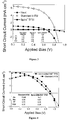
- Figure 1b shows the UV vis spectrum of the final [Spiro-OMeTAD] + [TFSI] - powder in chlorobenzene, proving that we have isolated a stable and fully oxidised version of Spiro-OMeTAD with a TFSI counter anion.
- the doping When employed as a dopant in the Spiro-OMeTAD HTM matrix, the doping will be irreversible, and completely independent of any atmospheric effects.
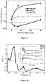
- Spiro-OMeTAD is p-doped by mixing a powder of pure Spiro-OMeTAD with the powdered oxidised salt of Spiro-OMeTAD produced by the method of Example 1. Mixture of the resultant powder with pure spiro-OMeTAD at varying concentrations results in changes in the conductivity of the material in the device configuration ( Figure 2 ). As expected, the conductivity of the Spiro-OMeTAD filled into a mesoporous TiO 2 structure increases and then decreases with increasing "doping" concentrations.
- a photovoltaic device in a "bilayer" structure comprised of a semiconducting absorber and an HTM layer, termed Meso-Super Structured Solar Cells (MSSCs) has been developed ( M. M. Lee, J. Teuscher, T. Miyasaka, T. N. Murakami and H. J. Snaith, Science, 2012 ).
- the absorber layer is formed over a 100 nm thick mesoporous alumina scaffold, and the hole transporting layer is simply deposited on top of this via spin coating.
- the additives are expected to be of far lesser importance at the interface.
- the only requirement of the HTM layer is that it have the appropriate HOMO level for hole transfer from the absorber, have a non-competing absorption, and have a high hole conductivity.
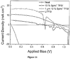
- FIG. 4 shows representative current density-voltage (JV) curves as well as the associated merit parameters of such solar cells prepared via the normal (LiTFSI and tbp) and "HTM salt only" (where 20 mol% spiro + TFSI - is used) routes. It is evident that the devices incorporating the spiro-OMeTAD + TFSI - perform similarly to those using the standard HTM composition. We expect that with further optimization, the results will continue to improve, and, as stated above, that the absence of extraneous additives such as Li-TFSI and tBP will aid in long-term stability.
- LiTFSI and tbp normal
- HTM salt only where 20 mol% spiro + TFSI - is used
- Example 1 - p-doping using protic ionic liquids (PILs).
- PILs protic ionic liquids
- Spiro-OMeTAD which is the state-of-the-art hole transporting material in ss-DSSCs.
- Figure 9 shows the conductivity of Spiro-OMeTAD as function of the ionic liquids content, as measured in inert atmosphere and dark condition. A fast growth is immediately visible for both H-TFSI and Himi-TFSI at low concentration, which reaches a plateau around 10 mol% with Spiro-OMeTAD.
- Et 4 N-TFSI tetraethyl bis(trifluoromethylsulfonyl)amide
- H-TFSI is highly sensitive to the air moisture and just few minutes of air exposure could significantly hydrate it.
- 90 mM solution of Spiro-OMeTAD in chlorobenzyl was prepared stirring the mixture overnight at 70°C.
- Solutions of ionic liquids (H-TFSI, Himi-TFSI and Et 4 N-TFSI) and Li-TFSI in acetonitrile have been prepared varying the concentration in order to add always the same amount (1/10 of the final volume) of dopant solution (in acetonitrile) to the Spiro-OMeTAD solution (in chlorobenzyl).
- Spiro-OMeTAD solutions with differs amount of dopant were spin-coated at 2000 rpm into mesoporous SiO 2 layer prepared on glass slides (particle size 40 nm, mesoporous layer thickness 300 nm) and dried at 140 °C for 30 min in inert atmosphere. Silver contacts (150 nm thick) were applied via thermal evaporation through a shadow mask in 2 ⁇ 10 -6 Torr vacuum.
- the electrode pattern was designed for four point probe measurements with a force channel length (direction of current flow) of 1 mm and a width of 1 cm, and a sense channel length of 300 ⁇ m and width of 1 mm.
- the sample preparation was identical to that described for the preparation of devices for conductivity measurements, with the exception that no silver electrodes were deposited on the top of the sample. All the samples were prepared in inert atmosphere and in filtered UV light condition. Absorbance measurements of the films were taken in air (about 1 min air exposure) using a commercial spectrophotometer (Varian Cary 300 UV- Vis, USA). Baseline measurements were performed on mesoporous SiO 2 substrate without Spiro-OMeTAD.
- FTO substrates (7 ⁇ /sq, Pilkington US) were etched with zinc powder and HCl (2 M aqueous solution) to give the desired electrode patterning.
- the substrates were cleaned with Hellmanex (2% by volume in water, Aldrich), de-ionized water, acetone, and ethanol. The last traces of organic residues were removed by a 10 minutes oxygen plasma cleaning step.
- the FTO sheets were subsequently coated with a compact layer of TiO 2 (about 30 nm) by aerosol spray pyrolysis deposition at 275 °C, using oxygen as the carrier gas.
- the Spiro-OMeTAD was applied by spin-coating at 1000 rpm for 45 s in air from solution prepared as previously described. After drying overnight, back contacts were applied by thermal evaporation of 150 nm of silver.
- Example 6 Meso-Superstructures Solar Cells (MSSCs) fabrication.
- FTO substrates (7 ⁇ /sq, Pilkington US) were etched with zinc powder and HCl (2 M aqueous solution) to give the desired electrode patterning.
- the substrates were cleaned with Hellmanex (2% by volume in water, Aldrich), de-ionized water, acetone, and ethanol. The last traces of organic residues were removed by a 10 min oxygen plasma cleaning step.
- the FTO sheets were subsequently coated with a compact layer of TiO 2 (about 30 nm) by aerosol spray pyrolysis deposition at 270 °C, using oxygen as the carrier gas.
- the TiO 2 films were slowly heated to 500 °C and allowed to sinter for 30 min in air.
- simulated AM 1.5 sunlight was generated with a class AAB ABET solar simulator calibrated to give simulated AM1.5, 100 mWcm -2 irradiance, using an NREL-calibrated KG5 filtered silicon reference cell, with less than 1% mismatch factor; the current-voltage curves were recorded with a sourcemeter (Keithley 2400, USA).
- the solar cells were masked with a metal aperture defining the active area (0.08 cm 2 ) of the solar cells. MSSCs were measured immediately after the thermal evaporation of electrodes.
- Li + lithium bis(trifluoromethylsulfonyl)-imide
- Li + lithium bis(trifluoromethylsulfonyl)-imide
- Li + has been reported as essential for device operation, since it helps lowering the series resistances and enhancing the photocurrent generation.
- Li + is redox active p-dopant, since it forms neutral lithium oxide species oxidising (p-doping) the Spiro-OMeTAD.
- the first is attributed to a downshift of the Fermi level of the electrons due to the positive charges (Li + ) at TiO 2 interface, the latter is explained as the result of an increased DOS below the conduction band due to Li + intercalation in the TiO 2 .
- the H + can more or less strongly affects the DOS in the TiO 2 , depending on the acid character of the employed PIL as shown in Figure 11 for H-TFSI and Himi-TFSI.
- the protonation of the metal oxides surface has been reported resulting in increased DOS below the conduction band, as well as observed for Li + .
- the DOS looks different from the previously described dopants, as shown for Et 4 N-TFSI.
- the voltage first rapidly grows with capacitance, and then it remains nearly constant about 0.95 V with further increase in capacitance. This could be explained considering that in the first regime the electrons injected in the TiO 2 are filling the narrow DOS of the conduction band edges, and then they are injected in the effective conduction band.
- JV characteristic current-voltage
- the short circuit photocurrent density shows a monotonic growth moving from the Et 4 N-TFSI to H-TFSI. This trend could be explained considering the shift of the electron Fermi level in the TiO 2 for different additives as described in Figure 11 . As widely reported in literature, a downshift of the Fermi level in the TiO 2 result in a more favourable electron injection from the dye excited state to the metal oxide.
- the J sc for Li-TFSI according to the DOS, is located between the Himi-TFSI and H-TFSI.
- open circuit voltage V oc
- the fill factor could be explained considering both the charge recombination and the device series resistance due to the hole transport.
- the device series resistance are very similar, as could be extracted by the slope of the JV in open circuit condition.
- the conductivity of the Spiro-OMeTAD with Li-TFSI and H-TFSI are very similar after leaving the device in air for one week.
- the lower fill factor for H-TFSI could be explained considering the recombination lifetime as reported in Figure 11 .
- Li-TFSI is recombining faster than H-TFSI, the latter can reach higher charge density, which give more recombination.
- Himi-TFSI and Et4N-TFSI are suffering both high recombination and series resistance, which result in a poor fill factor.
- the overall efficiency shows that H-TFSI and Li-TFSI are performing very close, then Himi-TFSI and Et 4 N-TFSI.
- the [TFSI] - and [SbCl 6 ] - salts of spiro-OMeTAD were prepared by the methods described above, except that no anion exchange was performed for producing the [SbCl 6 ] - salt.
- the anion exchange for the TFSI salt was performed by using 10 times excess tetraethylammonium TFSI.
- a thin 200 nm mesoporous scaffold was used to allow for good film formation of a film of the doped semiconductor which was approximately 1 ⁇ m thick.
- Figure 12 plots the conductivity of films of Spiro-OMeTAD at different doping fractions.
- the conductivities for films doped with Spiro + TFSI - are 2-3 times higher than the conductivities for those doped with Spiro + SbCl 6 - .
- the maximum conductivity reached using Spiro + TFSI - is almost 3 times higher than that using the previous best system: LiTFSI.
- Dye sensitized cells were constructed by the method described above (Example 10) and had the structure FTO, TiO 2 compact layer, mesoporous TiO 2 , D102 sensitising dye, doped organic semiconductor (hole transporter) and silver electrodes.
- the thickness of the hole transporter layer was from 300 to 500 nm thick.
- Figure 13 shows the characteristic current density-voltage (J-V) curves for dye sensitized solar cells made using the Spiro + TFSI - doping method, and incorporating no LiTFSI.
- EMIM TFSI (1-Ethyl-3-methylimidazolium bis(trifluoromethylsulfonyl)imide) is used to facilitate charge generation at the dye-TiO 2 interface but has very little influence on the conductivity of the hole transporter, as can be observed by the 650 ohm series resistance in devices with only this additive. Performance characteristics of the cells were as follows.
- FIG 14 shows characteristic current density-voltage (J-V) curves for mesosuperstructured solar cells (MSSCs) made using an organometal trihalide perovskite semiconductor when the Spiro + TFSI - doping method is used to prepare the HTM (hole transport material) layers.
- the devices were constructed by the method described above (Example 11) and had the structure FTO, compact TiO 2 layer, 400 nm mesoporous Al 2 O 3 layer, methylammonium lead triiodide perovskite absorber layer, doped organic semiconductor (hole transporter) and silver electrodes. No other additives are present.
- the thickness of the hole transporter layer was from 300 to 500 nm thick, unless specified as 1 ⁇ m thick.
- the doping percentage refers to a molar doping percentage of the HTM salt and the neutral HTM.
- the upper curve ( ⁇ ) corresponds to an MSSC fabricated with a 1 micrometer thick hole transporter layer, which should make such cells more stable to water ingress. Making such thick layers is possible because of the superior conductivity of the HTM layers when doped with the oxidized HTM salt.
- the thickest HTM layer with the conventional LiTFSI dopant is around 400 nm before the device begins to suffer from low fill factors (data not shown). Performance characteristics of the cells were as follows.
- MSSCs Complete mesosuperstructured solar cells
- the MSSCs were produced by the same method and with the same structure as in Example 17, except that the silver electrodes were evaporated after thermal stressing.
- Figure 15 shows a photograph of these complete cells following the heat treatment.
- the solar cell where the LiTFSI dopant is used has rapidly degraded because the hydroscopic LiTFSI salt leads to high water content in the perovskite film, so that the perovskite layer is degraded to PbI 2 (explaining the observed yellow color).
- Solar cells prepared with the oxidized HTM salt as dopant are clearly far more stable to moisture ingress and thermal treatment.
- FIG 16 shows the characteristic current density-voltage (J-V) curves for the mesosuperstructured solar cells described above and shown in Figure 15 .
- the solar cells using LiTFSI to dope the HTM do not function at all, as is expected from the degradation evident in the photograph ( Figure 15 ).
- the solar cells protected by the thick 1 micron layer of HTM doped with 10 % Spiro + TFSI - have withstood the thermal stressing the best, still delivering over 7 % power conversion efficiency.
- the performance characteristics of these devices are as follows.
Landscapes
- Engineering & Computer Science (AREA)
- Chemical & Material Sciences (AREA)
- Materials Engineering (AREA)
- Power Engineering (AREA)
- Microelectronics & Electronic Packaging (AREA)
- Manufacturing & Machinery (AREA)
- Physics & Mathematics (AREA)
- Spectroscopy & Molecular Physics (AREA)
- Inorganic Chemistry (AREA)
- Electromagnetism (AREA)
- Photovoltaic Devices (AREA)
- Organic Low-Molecular-Weight Compounds And Preparation Thereof (AREA)
Description
- The present invention relates to processes for the production of p-doped organic semiconductors. The invention also relates to a process for producing layers of p-doped organic semiconductors. Processes for producing devices comprising p-doped organic semiconductors and layers thereof are also disclosed, along with compositions, layers and devices.
- The work leading to this invention has received funding from the European Research Council under the European Union's Seventh Framework Programme (FP7/2007-2013)/ERC grant agreement No.
279881 - Organic semiconductors (OSs) are now controlling the electronics market in different stages of development for a wide range of applications and are expected to dominate over the next few decades. Key factors driving penetration of organic electronics in the mainstream market are their low cost for fabrication and high degree of flexibility. Since their sensational discovery in 1977 several studies have shown the possibility to modulate their properties for the specific application using chemical doping. Conceptually similar to inorganic semiconductors, chemical doping introduces impurities into the organic semiconductors which increase the density of mobile charge carriers and thus conductivity. In reality, chemical doping can involve several different mechanisms depending on both the semiconductor and the dopant. One of the first described mechanisms was the protonic acid (H+) doping of polyacetylene. This was accomplished by immersing polyacetylene in an aqueous hydrochloric acid solution. Drying the polymer leaves residual H3O+ groups in the organic matrix which increase the density of mobile charge carriers by partially withdrawing electrons from the conjugated chains. The resulting p-doped organic semiconductor shows an increase in conductivity of around 10 orders of magnitude. Following this, H+ treatment has been reported as a general doping route for many conjugated polymers. Recently, several heterocyclic organic hydrides have been reported as efficient n-type dopants by releasing hydride (H-) or hydrogen atoms (H•) (P. Wei, J. H. Oh, G. Dong and Z. Bao, Journal of the American Chemical Society, 2010, 132, 8852-8853). In particular, 1,3-dimethyl-2-phenyl-2,3-dihydro-1H-benzoimidazole derivatives (DMBI) can increase the conductivity of [6,6]-phenyl C61 butyric acid methyl ester (PCBM) by more than 4 order of magnitude. After the H• release, the highly energetic DMBI radicals can inject electrons in the PCBM increasing the density of mobile charge carriers in the organic semiconductor matrix. The stability of this doping mechanism depends on the rate of back electron transfer from the doped PCBM to the DMBI cation, which can be stabilized by electron-rich substituent on DMBI core. This mechanism has been effectively applied to prepare air stable organic thin film transistors. Many other organic electronic applications can benefit from chemical doping: e.g., triphenylamine-based organic semiconductors have been p-doped with Co(III) complexes in solid-state dye-sensitized solar cells (ss-DSSCs) (J. Burschka, A. Dualeh, F. Kessler, E. Baranoff, N. L. Cevey-Ha, C. Yi, M. K. Nazeeruddin and M. Grätzel, Journal of the American Chemical Society, 2011) and tetracyano-quinoline derivatives in organic light emitting diodes (B. W. DAndrade, S. R. Forrest and A. B. Chwang, Applied physics letters, 2003, 83, 3858-3860). Both applications benefit from the introduction of a p-doped transport layer since it reduces the charge transport resistance in series with the p-n junction and helps to achieve ohmic contacts. Furthermore, chemical doping also enables the fabrication of tandem structures for efficient organic solar cells using a versatile recombination contact.
- However, most of the dopants reported in scientific literature have never been effectively applied in electronic device, since they are incompatible with solution-processed materials or they demonstrate weak doping effects, which makes the device unstable in working conditions. Due to the beneficial characteristics of protic ionic liquids (PILs), such as good solvation and strong acidity, solution-processable and effective doping techniques have been found using PILs.
- Organic semiconductors (OSs) are commonly employed in photovoltaics, organic light emitting diodes (LEDs), and organic transistors. One family of commonly employed organic semiconductors as hole transporting materials (HTMs) are triphenylamines (also known as triarylamines) and their derivatives. These have been successfully employed in dye-sensitized solar cells (U. Bach, D. Lupo, P. Comte, J. E. Moser, F. Weissortel, J. Salbeck, H. Spreitzer and M. Gratzel, Nature, 1998, 395, 583-585). Triphenylamine derivatives often benefit from wide bandgaps and easily tunable HOMO levels, making them especially promising as HTMs for solid-state dye-sensitized solar cells (ss-DSSCs) where the light is absorbed by a sensitizing dye. However, this class of HTMs suffers from low hole mobilities, with one of the most commonly employed triphenylamine HTM (spiro-OMeTAD) having mobilities between 10-5 and 10-4 cm2 V-1s-1 in working device conditions. As a result, these materials have been doped by a variety of molecular oxidants in attempts to minimize the resistance to charge transport in the HTM component of ss-DSSCs (U. Bach, EPFL, 2000; H. J. Snaith et al., Nano Letters, 2006, 6, 2000-2003).
- However, these "in situ" doping approaches have several drawbacks. It is difficult to establish the efficiency of the oxidation, and it is difficult to distinguish what degree of oxidation occurs in the initial HTM spin-coating solution compared to in the final film. The long-term stability of the oxidised product in the final device structure is often poor, or may even vary with ambient conditions such as humidity, temperature and light exposure. Moreover, these approaches to doping result in the oxidation products staying in the film, so that the final device incorporates impurities that do not serve any beneficial function and may even hinder device performance and long-term stability. As can be expected, these in-situ doping processes result in a great deal of variability in final device performance.
- Jiang et al, Chemical Physics Letters, 364, 5-6 (2002), 616-620 describes doping of poly(3-hexylthiophene) films. Margaretta et al, Journal of Applied Polymer Science, 127, 4 (2012), 2453-2457 describes the doping of polyaniline. Snaith et al, Applied Physics Letters, 89, 26 (2006), 262114 describes doping using a redox inactive dopant. Cappel, 12, 9 (2012), 4925-4931 describes oxygen-induced doping of spiro-OMeTAD. Tigelaar et al, Polymer, 47, 12 (2006), 4269-4275 describes the incorporation of protic ionic liquids in elastomeric polymers.
US 2012/0192945 A1 describes a photovoltaic element comprising a p-semiconductor which comprises silver in an oxidized form. - The invention relates to effective methods to p-dope organic semiconductors that can be employed in semiconducting devices, and which are typically employed as HTM's in dye-sensitized solar cells (DSSCs) and meso-super structured solar cells (MSSCs). The inventors have found that doping such organic semiconductors with a protic ionic liquid can be extremely effective.
- The invention provides a process for producing a p-doped organic semiconductor comprising chemically doping an organic semiconductor with a protic ionic liquid, wherein the protic ionic liquid is bis(trifluoromethanesulfonyl)imide (H-TFSI) and wherein the organic semiconductor comprises a compound of formula (Vb)

- The invention also provides a process for producing a layer of a p-doped organic semiconductor comprising disposing on a substrate an organic semiconductor comprising a compound of formula (Vb) and a protic ionic liquid which is H-TFSI.
- Further, the invention provides a layer of a p-doped organic semiconductor comprising an organic semiconductor comprising a compound of formula (Vb) and a protic ionic liquid which is H-TFSI.
- Also provided is a process for producing a semiconductor device comprising
a step of producing a p-doped organic semiconductor by a process according to the invention; or
a step of producing a layer of a p-doped organic semiconductor by a process according to the invention. - The process for producing a semiconductor device according to the invention may comprise:
- (a) disposing on a first electrode material at least one layer of a semiconductor material to produce a resulting substrate comprising a first electrode material and at least one layer of a semiconductor material;
- (b) sensitizing the resulting substrate to produce a sensitized substrate; and
- (c) producing a layer of a p-doped organic semiconductor on the sensitized substrate by a process according to the invention.
- Also provided is a semiconductor device which comprises a layer of a p-doped organic semiconductor wherein the layer of a p-doped semiconductor comprises an organic semiconductor comprising a compound of formula (Vb) and a protic ionic liquid which is H-TFSI.
-
-
Figure 1 shows (a) UV-vis spectra of Spiro-OMeTAD in chlorobenzene at varying oxidant (Sb) concentrations. (b) UV-vis spectrum of the Spiro-OMeTAD+ TFSI- product in chlorobenzene. -
Figure 2 shows the conductivity of Spiro-OMeTAD doped with varying mol% of Spiro-OMeTAD+ TFSI-. The dashed line indicates the conductivity of the commonly employed optimal HTM composition, with 20 mol% Li-TFSI as p-dopant. -
Figure 3 shows current density - voltage (JV) curves for neat Spiro-OMeTAD (filled black circles), the standard HTM composition (open black circles), and 20 mol% Spiro+ TFSI- doped HTM. Merit parameters are presented, where Jsc is the short circuit current (in mA cm-2), Voc is the open circuit voltage (in V), FF is the fill factor, and PCE is the power conversion efficiency (in %). -
Figure 4 shows JV curves of representative solar cells employing the mixed halide absorber on a 100 nm thin mesoporous alumina scaffold. Black squares represent the standard HTM composition using 20 mol% Li-TFSI and 0.08 M tBP (or 100 mol %), while red circles represent devices with the only HTM additive being 20 mol% of Spiro+ TFSI-. Merit parameters are presented, where Jsc is the short circuit current (in mA cm-2), Voc is the open circuit voltage (in V), FF is the fill factor, and PCE is the power conversion efficiency (in %). -
Figure 5 shows (a) Chemical structure of ionic liquids relating to the invention, bis(trifluoromethanesulfonyl)imide (H-TFSI) and 1-alkyl-3-methylimidazolium bis(trifluoromethylsulphonyl)amide (Himi-TFSI) which are protic ionic liquids (PILs), with H-TFSI more acidic then Himi-TFSI, and bis(trifluoromethylsulfonyl)amide (Et4N-TFSI) which is an aprotic ionic liquid, the pH scale may be considered as an indication of how strongly a proton will be transferred from the PIL to a base, though it must be noted that the pH is usually considered for aqueous solutions and may not be appropriate for the nonaqueous PILs; (b) chemical structure of the small moleculeorganic semiconductor 2,2',7,7'-tetrakis(N,N-di-p-methoxyphenyl-amine)9,9'-Spirobifluorene (Spiro-OMeTAD); (c) Conductivity for Spiro-OMeTAD against the content of different ionic liquids; (d) UV-Vis absorption spectra of Spiro-OMeTAD doped with H-TFSI and the absorption for the specific wavelengths as function of the H-TFSI concentration (inset). -
Figure 6 shows photocurrent-voltage curves for devices employing different additives. All the devices were sensitized with D102 and measured under AM1.5 simulated sun light of 100 mW cm-2 equivalent solar irradiance. -
Figure 7 shows photocurrent-voltage curves for devices employing the optimized additive composition Li-TFSI and tBP or Himi-TFSI. The devices were sensitized with D102 and measured under AM1.5 simulated sun light of 100 mW cm-2 equivalent solar irradiance. -
Figure 8 shows photocurrent-voltage curves for devices employing the optimized Li-TFSI additive composition or H-TFSI. The devices use perovskite photoactive layer as described in the experimental section. They have been measured under AM1.5 simulated sun light of 100 mW cm-2 equivalent solar irradiance. -
Figure 9 shows conductivity of doped Spiro-OMeTAD. -
Figure 10 shows UV-Vis absorption of Spiro-OMeTAD doped with H-TFSI. -
Figure 11 shows transient photo-voltage and photo-current decay measurements for devices employing Spiro-OMeTAD as hole transporter and different additives. -
Figure 12 shows the conductivity of spiro-OMeTAD films doped with different molar doping fractions of TFSI- or SbCl6 - salts of spiro-OMeTAD. -
Figure 13 shows photocurrent-voltage curves for dye sensitized solar cells employing varying levels of doping. -
Figure 14 shows photocurrent-voltage curves for mesosuperstructured solar cells employing varying levels of doping. -
Figure 15 shows a photograph of complete solar cells after exposure to ambient air (50% humidity) at 80°C for 18 hours. -
Figure 16 shows photocurrent-voltage curves for mesosuperstructured solar cells after exposure to ambient air (50% humidity) at 80°C for 18 hours. - The inventors have found that by chemically doping an organic semiconductor comprising a compound of formula (Vb) with a protic ionic liquid which is H-TFSI, the high conductivities required for effective semiconductor device performance may be achieved without the need for the addition of any extraneous additives. Furthermore, methods using the protic ionic liquid (PIL) produce doped organic semiconductors comprising a compound of formula (Vb) which show improved long-term atmospheric stability. Methods using the PIL are generally solution-processable due to the solubility of the PIL.
- In particular, the methods described herein allow the effects of p-doping the hole transport material/organic semiconductor to be separated from the effects of ionic additives on charge generation, separation and collection. This is a novel concept.
- The term "doping", as used herein, refers to a process of introducing impurities into a semiconductor in order to alter the electronic properties of the semiconductor. Often, impurities are introduced to increase the conductivity of the semiconductor. Doping alters the charge carrier concentration in the semiconductor. The term "p-doping", as used herein, refers to a doping process in which the impurities introduced increase the number of charge carriers which are holes or charge acceptors. When a semiconductor is p-doped it forms a semiconductor in a p-type region. P-doping introduces electron acceptors into the semiconductor. This is in contrast to n-doping which introduces electron donors into the semiconductor. Cationic forms of organic semiconductor molecules, be they protonated or ionised, may act as p-dopants by accepting electrons from the organic semiconductor. P-doped organic semiconductors are useful as they may act as hole transport materials (HTMs). The terms "p-doped organic semiconductor" and "hole transport material" may be used interchangeably herein.
- The term "organic semiconductor", as used herein, refers to an organic material with electrical conductivity intermediate in magnitude between that of a conductor and an insulator. Typically, an organic semiconductor is an organic material that has a conductivity of from 103 to 10-8 Scm-1. Standard techniques such as a 4-point probe conductivity measurement may be used to measure conductivity. The term "organic material", as used herein, refers to a material which comprises mostly (e.g. greater than 50 wt% or greater than 80 wt%) of one or more organic compounds. Typically an organic semiconductor will comprise greater than 90 wt% of one or more organic compounds. Materials used as semiconductors are often of high purity and accordingly an organic semiconductor may be a semiconducting material which consists essentially of an organic compound with semiconducting properties. Organic semiconductors may comprise one or more organic compounds with semiconducting properties, but often comprise or consist essentially of a single organic compound.
- The term "consisting essentially of', as used herein, refers to a composition consisting of the given components together with any other components which are not specified provided that these additional components do not have a material affect on the functioning of the composition and are present in an amount of less than 2 wt%.
- The organic semiconductor comprises a compound of formula (Vb)

- The term "aryl ring", used herein, refers to any monocyclic or polycyclic hydrocarbon compound, at least one ring of which is an aromatic ring. An aryl ring has from 6 to 30 carbons. Examples of aryl rings aromatic hydrocarbon compound such as benzene, indene, naphthene, azulene, fluorene, anthracene, phenanthrene, pyrene, acenaphthylene, benz[a]anthracene, benzo[a]pyrene, benzo[e]pyrene, benzo[b]fluoranthene, benzo[ghi]perylene, benzo[j]fluoranthene, benzo[k]fluoranthene, chrysene, coronene, dibenz(a,h)anthracene, fluoranthene, indeno(1,2,3-cd)pyrene, and biphenyl. When an aryl ring appears in a formula, each bond coming off the ring will be formed to a carbon in the ring. An unsubstituted or substituted aryl ring may be unsubstituted or substituted benzene, unsubstituted or substituted naphthalene, unsubstituted or substituted anthracene, unsubstituted or substituted pyrene, or unsubstituted or substituted biphenyl.
- The term "heteroaryl ring", used herein, refers to any monocyclic or polycyclic aryl compound, at least one ring of which is an aromatic ring containing a heteroatom. Heteroatoms include N, O, S and P. Often, the heteroatom is N. A heteroaryl ring has from 6 to 30 carbons and 1 or more, often 1 to 10, heteroatoms which may each be the same or different heteroatom. Examples of heteroaryl rings include compounds such as benzene, indene, naphthene, azulene, fluorene, anthracene, phenanthrene, pyrene, acenaphthylene, benz[a]anthracene, benzo[a]pyrene, benzo[e]pyrene, benzo[b]fluoranthene, benzo[ghi]perylene, benzo[j]fluoranthene, benzo[k]fluoranthene, chrysene, coronene, dibenz(a,h)anthracene, fluoranthene, indeno(1,2,3-cd)pyrene, and biphenyl in which one or more carbon atom has been replaced with a heteroatom. Examples of unsubstituted or substituted heteroaryl rings include rings derived from unsubstituted or substituted furan, thiophene, pyrrole, oxazole, thiazole, imidazole, pyrazole, isoxazole, isothiazole, pyridine, 2,2-bipyridine, pyridazine, pyrimidine, pyrazine, indolizine, indole, isoindole, benzo[b]furan, benzo[b]thiophene, purine, quinolizine, quinoline, isoquinoline, carbazole, acridine, phenazine, phenothiazine, or phenoxazine. In particular, heteroaryl rings pyridine, pyrrole and thiophene.
- When an aryl or heteroaryl ring as defined above is substituted it typically bears one or more substituents selected from C1-C8 alkyl, C2-C8 alkenyl, C2-C8 alkynyl, C3-8 cylcloalkyl, C3-8 heterocylcloalkyl, aryl, heteroaryl, cyano, amino, azide, C1-8 alkylamino, di(C1-8)alkylamino, arylamino, diarylamino, arylalkylamino, amido, acylamido, hydroxy, halo, carboxy, ester, acyl, acyloxy, C1-8 alkoxy, aryloxy, haloalkyl, thiol, C1-8 alkylthio, arylthio, sulfonic acid, phosphoric acid, phosphate ester, phosphonic acid, phosphonate ester and sulfonyl. Typically it carries 0, 1, 2 or 3 substituents. A substituted aryl or heteroaryl ring may be substituted in two positions with a single C1-7 alkylene group, or with a bidentate group represented by the formula -X-C1-7 alkylene, or -X-C1-7 alkylene-X-, wherein X is selected from O, S and NR, and wherein R is H, aryl or C1-6 alkyl. Thus a substituted aryl ring may be an aryl ring fused with a cycloalkyl group or with a heterocyclyl group. The term aralkyl as used herein, pertains to an aryl group in which at least one hydrogen atom (e.g., 1, 2, or 3) has been substituted with a C1-6 alkyl group. Examples of such groups include, but are not limited to, tolyl (from toluene), xylyl (from xylene), mesityl (from mesitylene), and cumenyl (or cumyl, from cumene), and duryl (from durene). The term "aryl group", as used herein, refers to a group derived from an aryl ring as defined herein. The term "heteroaryl group", as used herein, refers to a group derived from a heteroaryl ring as defined herein.
- When a group is substituted it typically bears one or more substituents selected from C1-C8 alkyl, C2-C8 alkenyl, C2-C8 alkynyl, C3-8 cylcloalkyl, C3-8 heterocylcloalkyl, aryl, heteroaryl, cyano, amino, azide, C1-8 alkylamino, di(C1-8)alkylamino, arylamino, diarylamino, arylalkylamino, amido, acylamido, hydroxy, halo, carboxy, ester, acyl, acyloxy, C1-8 alkoxy, aryloxy, haloalkyl, sulfhydryl, C1-8 alkylthio, arylthio, sulfonic acid, phosphoric acid, phosphate ester, phosphonic acid, phosphonate ester and sulfonyl. Typically it carries 0, 1, 2 or 3 substituents.
- The term "C1-8 alkyl group", as used herein, refers to a straight or branched chain saturated hydrocarbon group. Typically it is methyl, ethyl, propyl, butyl, pentyl, hexyl, heptyl, or octyl, or C1-6 alkyl, for example methyl, ethyl, propyl, butyl, pentyl or hexyl, or C1-4 alkyl, for example methyl, ethyl, i-propyl, n-propyl, t-butyl, s-butyl or n-butyl. When an alkyl group is substituted it typically bears one or more substituents selected from those described above for substituted aryl or heteroaryl rings, wherein the substituents are optionally unsubstituted.
- The term "C2-8 alkenyl group", as used herein, refers to a C2-8 alkyl group as defined above, wherein the group contains one or more double bonds. The term "C2-8 alkynyl group", as used herein, refers to a C2-8 alkyl group as defined above, wherein the group contains one or more triple bonds. Typically a substituted alkyl group, alkenyl group or alkynyl group carries 1, 2 or 3 substituents, for
instance - A C3-8 cycloalkyl group is an unsubstituted or substituted alkyl group which is also a cyclyl group; that is, a monovalent moiety obtained by removing a hydrogen atom from an alicyclic ring atom of a carbocyclic ring of a carbocyclic compound, which moiety has from 3 to 8 carbon atoms, including from 3 to 8 ring atoms. Thus, the term "cycloalkyl" includes the sub-classes cycloalkyenyl and cycloalkynyl. Examples of C3-8 cycloalkyl groups include, but are not limited to, those derived from saturated monocyclic hydrocarbon compounds, which C3-8 cycloalkyl groups are unsubstituted or substituted as defined above for aryl or heteroaryl groups:
cyclopropane (C3), cyclobutane (C4), cyclopentane (C5), cyclohexane (C6), cycloheptane (C7), methylcyclopropane (C4), dimethylcyclopropane (C5), methylcyclobutane (C5), dimethylcyclobutane (C6), methylcyclopentane (C6), dimethylcyclopentane (C7), methylcyclohexane (C7), dimethylcyclohexane (C8);
unsaturated monocyclic hydrocarbon compounds:
cyclopropene (C3), cyclobutene (C4), cyclopentene (C5), cyclohexene (C6), methylcyclopropene (C4), dimethylcyclopropene (C5), methylcyclobutene (C5), dimethylcyclobutene (C6), methylcyclopentene (C6), dimethylcyclopentene (C7), methylcyclohexene (C7), dimethylcyclohexene (C8). - A C3-8 heterocyclyl group is an unsubstituted or substituted monovalent moiety obtained by removing a hydrogen atom from a ring atom of a heterocyclic compound, which moiety has from 3 to 8 ring atoms, of which from 1 to 5 are ring heteroatoms.
- Examples of (non-aromatic) monocyclic C3-8 heterocyclyl groups include, but are not limited to, those derived from:
- N1: aziridine (C3), azetidine (C4), pyrrolidine (tetrahydropyrrole) (C5), pyrroline (e.g., 3-pyrroline, 2,5-dihydropyrrole) (C5), 2H-pyrrole or 3H-pyrrole (isopyrrole, isoazole) (C5), piperidine (C6), dihydropyridine (C6), tetrahydropyridine (C6), azepine (C7);
- O1: oxirane (C3), oxetane (C4), oxolane (tetrahydrofuran) (C5), oxole (dihydrofuran) (C5), oxane (tetrahydropyran) (C6), dihydropyran (C6), pyran (C6), oxepin (C7);
- S1: thiirane (C3), thietane (C4), thiolane (tetrahydrothiophene) (C5), thiane (tetrahydrothiopyran) (C6), thiepane (C7);
- O2: dioxolane (C5), dioxane (C6), and dioxepane (C7);
- O3: trioxane (C6);
- N2: imidazolidine (C5), pyrazolidine (diazolidine) (C5), imidazoline (C5), pyrazoline (dihydropyrazole) (C5), piperazine (C6);
- N1O1: tetrahydrooxazole (C5), dihydrooxazole (C5), tetrahydroisoxazole (C5), dihydroisoxazole (C5), morpholine (C6), tetrahydrooxazine (C6), dihydrooxazine (C6), oxazine (C6);
- N1S1: thiazoline (C5), thiazolidine (C5), thiomorpholine (C6);
- N2O1: oxadiazine (C6);
- O1S1: oxathiole (C5) and oxathiane (thioxane) (C6); and,
- N1O1S1: oxathiazine (C6).
- Examples of linear saturated C1-7 alkylene groups include, but are not limited to, -(CH2)n- where n is an integer from 1 to 7, for example, -CH2- (methylene), -CH2CH2-(ethylene), -CH2CH2CH2- (propylene), and -CH2CH2CH2CH2- (butylene). Examples of branched saturated C1-7 alkylene groups include, but are not limited to, -CH(CH3)-, -CH(CH3)CH2-, -CH(CH3)CH2CH2-, -CH(CH3)CH2CH2CH2-, -CH2CH(CH3)CH2-, -CH2CH(CH3)CH2CH2-, -CH(CH2CH3)-, -CH(CH2CH3)CH2-, and -CH2CH(CH2CH3)CH2-.
- Examples of linear partially unsaturated C1-7 alkylene groups include, but is not limited to, -CH=CH- (vinylene), -CH=CH-CH2-, -CH2-CH=CH2-, -CH=CH-CH2-CH2-, -CH=CH-CH2-CH2-CH2-, -CH=CH-CH=CH-, -CH=CH-CH=CH-CH2-, -CH=CH-CH=CH-CH2-CH2-, -CH=CH-CH2-CH=CH-, and -CH=CH-CH2-CH2-CH=CH-.
- Examples of branched partially unsaturated C1-7 alkylene groups include, but is not limited to, -C(CH3)=CH-, -C(CH3)=CH-CH2-, and -CH=CH-CH(CH3)-. Examples of alicyclic saturated C1-7 alkylene groups include, but are not limited to, cyclopentylene (e.g., cyclopent-1,3-ylene), and cyclohexylene (e.g., cyclohex-1,4-ylene). Examples of alicyclic partially unsaturated C1-7 alkylene groups include, but are not limited to, cyclopentenylene (e.g., 4-cyclopenten-1,3-ylene), cyclohexenylene (e.g., 2-cyclohexen-1,4-ylene; 3-cyclohexen-1,2-ylene; 2,5-cyclohexadien-1,4-ylene).
- In this context, the prefixes (e.g., C1-6, C3-8 etc.) denote the number of ring atoms, or range of number of ring atoms, whether carbon atoms or heteroatoms.
- As used herein the term "oxo" represents a group of formula: =O
- As used herein the term "acyl" represents a group of formula: -C(=O)R, wherein R is an acyl substituent, for example, a substituted or unsubstituted C1-8 alkyl group, a substituted or unsubstituted C3-8 heterocyclyl group, or a substituted or unsubstituted aryl group. Examples of acyl groups include, but are not limited to, -C(=O)CH3 (acetyl), -C(=O)CH2CH3 (propionyl), -C(=O)C(CH3)3 (t-butyryl), and -C(=O)Ph (benzoyl, phenone). As used herein the term "acyloxy" represents a group of formula: -OC(=O)R, wherein R is an acyloxy substituent, for example, substituted or unsubstituted C1-8 alkyl group, a substituted or unsubstituted C3-8 heterocyclyl group, or a substituted or unsubstituted aryl group, typically a C1-6 alkyl group. Examples of acyloxy groups include, but are not limited to, -OC(=O)CH3 (acetoxy), -OC(=O)CH2CH3, -OC(=O)C(CH3)3, -OC(=O)Ph, and -OC(=O)CH2Ph.
- As used herein the term "ester" (or "carboxylate", "carboxylic acid ester" or "oxycarbonyl") represents a group of formula: -C(=O)OR, wherein R is an ester substituent, for example, a substituted or unsubstituted C1-8 alkyl group, a substituted or unsubstituted C3-8 heterocyclyl group, or a substituted or unsubstituted aryl group (typically a phenyl group). Examples of ester groups include, but are not limited to, -C(=O)OCH3, -C(=O)OCH2CH3, -C(=O)OC(CH3)3, and -C(=O)OPh.
- As used herein the term "amino" represents a group of formula -NH2. The "term C1-C8 alkylamino" represents a group of formula -NHR' wherein R' is a C1-8 alkyl group, preferably a C1-6 alkyl group, as defined previously. The term "di(C1-8)alkylamino" represents a group of formula -NR'R" wherein R' and R" are the same or different and represent C1-8 alkyl groups, preferably C1-6 alkyl groups, as defined previously. The term "arylamino" represents a group of formula -NHR' wherein R' is an aryl group, preferably a phenyl group, as defined previously. The term "diarylamino" represents a group of formula -NR'R" wherein R' and R" are the same or different and represent aryl groups, preferably phenyl groups, as defined previously. The term "arylalkylamino" represents a group of formula -NR'R" wherein R' is a C1-8 alkyl group, preferably a C1-6 alkyl group, and R" is an aryl group, preferably a phenyl group.
- A halo group is chlorine, fluorine, bromine or iodine (a chloro group, a fluoro group, a bromo group or an iodo group). It is typically chlorine, fluorine or bromine.
- As used herein the term "amido" represents a group of formula: -C(=O)NR'R", wherein R' and R" are independently amino substituents, as defined for di(C1-8)alkylamino groups. Examples of amido groups include, but are not limited to, -C(=O)NH2, -C(=O)NHCH3, -C(=O)N(CH3)2, -C(=O)NHCH2CH3, and -C(=O)N(CH2CH3)2, as well as amido groups in which R' and R", together with the nitrogen atom to which they are attached, form a heterocyclic structure as in, for example, piperidinocarbonyl, morpholinocarbonyl, thiomorpholinocarbonyl, and piperazinocarbonyl.
- As used herein the term "acylamido" represents a group of formula: -NR1C(=O)R2, wherein R1 is an amide substituent, for example, hydrogen, a C1-8 alkyl group, a C3-8 heterocyclyl group, an aryl group, preferably hydrogen or a C1-8 alkyl group, and R2 is an acyl substituent, for example, a C1-8 alkyl group, a C3-8 heterocyclyl group, or an aryl group, preferably hydrogen or a C1-8 alkyl group. Examples of acylamide groups include, but are not limited to, -NHC(=O)CH3, -NHC(=O)CH2CH3, -NHC(=O)Ph, and -NHC(=O)C4H9. Thus, a substituted C1-8 alkyl group may comprise an acylamido substituent defined by the formula -NHC(=O)-C1-8 alkyl, such as -NHC(=O)C2H5. R1 and R2 may together form a cyclic structure, as in, for example, succinimidyl, maleimidyl, and phthalimidyl:

- A C1-8 alkylthio group is a said C1-8 alkyl group, preferably a C1-6 alkyl group, attached to a thio group. An arylthio group is an aryl group, preferably a phenyl group, attached to a thio group.
- A C1-8 alkoxy group is a said substituted or unsubstituted C1-8 alkyl group attached to an oxygen atom. A C1-6 alkoxy group is a said substituted or unsubstituted C1-6 alkyl group attached to an oxygen atom. A C1-4 alkoxy group is a substituted or unsubstituted C1-4 alkyl group attached to an oxygen atom. Examples of C1-4 alkoxy groups include, -OMe (methoxy), -OEt (ethoxy), -O(nPr)(n-propoxy), -O(iPr) (isopropoxy), -O(nBu) (n-butoxy), - O(sBu) (sec-butoxy), -O(iBu) (isobutoxy), and -O(tBu) (tert-butoxy). An aryloxy group is a substituted or unsubstituted aryl group, as defined herein, attached to an oxygen atom. An example of an aryloxy group is -OPh (phenoxy).
- If a defined group is substituted with A, and A is substituted with B, then the substituent B is typically unsubstituted.
- The term "treating", as used herein, refers to any process in which one compound is allowed to react or interact with another. This may be done through any appropriate process. Treating includes, inter alia, exposing two or more reagents to each other, mixing two or more reagents in their solid state, adding a solution of one or more reagents to a solid form of the other, adding a solid of one or more reagents to a solution of another, mixing solutions of two or more reagents, or mixing solutions of two or more reagents and then adding a solid of a third and optionally further reagents. One of the listed reagents by which another is treated may be added as the reagent itself, or may be added as a precursor that converts by some process to the reagent itself. Therefore, treating a compound A with a compound B includes treating compound A with a precursor to compound B which converts to compound B by any method, including, inter alia, converting to B when dissolved, converting to B due to exposure to A, converting to B under basic or acidic conditions, and converting to B over time in a decomposition type process. Treating with a compound also includes any process wherein the process comprises adding that compound, regardless of whether that compound converts to another compound before undergoing a reaction.
- Preferably, when used herein, the anion A is ClO4 -, NO3 - or an anion of formula (i), (ii), (iii) or (iv):


- The term "electron withdrawing group" (EWG), as used herein, refers to a group which will reduce the electron density on the moiety to which it is bonded by drawing electrons away. An EWG may withdraw electrons through pi-conjugation, or by containing atoms with a higher electronegativity than the atoms to which they are bonded. Examples of electron withdrawing groups include halogen atoms (F, Cl, Br or I), groups comprising halogen atoms (e.g. CY3 or C2Y5 where each Y is a halogen atom), carbonyl groups (e.g. - C(O)-R) or cyano groups (-CN). If two X groups are present, they may be bonded to each other to form a ring. In one embodiment X is a C1-8-haloalkyl group, preferably wherein the proximal carbon atom bears one or two halogen atoms. Preferably, when X is a C1-8-haloalkyl group it is a C1-8 perhaloalkyl group. A C1-8 perhaloalkyl group is a C1-8-haloalkyl group in which all of the hydrogen atoms have been replaced with halogen atoms, typically fluorine atoms. Often, X is a group selected from Y, CH2Y, CHY2, CY3, CY2CY3, CY2CY2CY3 or CY2CY2CY2CY3 and each Y is the same or different and is F or Cl. X may be CF3, CF2CF3 or CF2CF2CF3. Preferably, X is CF3 or CF2CF3.
- Often it is preferred that the anion A is an anion of formula (i) wherein X is an EWG. Typically, A is an anion of formula (i) wherein X is a C1-8-perhaloalkyl group. Often, A is an anion of formula (i) wherein X is CF3 or CF2CF3. Therefore, preferably, A is bis(trifluoromethanesulfonyl)imide (TFSI) or bis(pentafluoroethanesulfonyl)imide (BETI). Alternatively, A is an anion selected from trifluoroacetate, trifluoromethanesulfonate, bis(trifluoromethanesulfonyl)imide, bis(pentafluoroethanesulfonyl)imide, or bis(perfluoropropanesulfonyl)imide. In one embodiment, A is bis(trifluoromethanesulfonyl)imide, bis(pentafluoroethanesulfonyl)imide, bis(perfluoropropanesulfonyl)imide, trifluoroacetate, or trifluoromethanesulfonate. The bis(trifluoromethanesulfonyl)imide anion has the following formula:

- The term "organic solvent", as used herein, refers to a solvent the molecules of which comprise at least one carbon atom and typically at least one hydrogen atom. The term is well known. The organic solvent may be an alcohol, a thiol, an ether, a ketone, an aldehyde, an alkane, a cycloalkane, an aromatic hydrocarbon, a halogenated aromatic hydrocarbon, a heterocyclic compound, an aromatic heterocyclic compound, a halogenated hydrocarbon, a nitrile or an amine. The term "alcohol", as used herein, refers to a compound which comprises one or more hydroxyl groups. Examples of such compounds include C1-C8-alcohols, for instance methanol or ethanol. Di-, tri- and poly-ols are also included (e.g. ethylene glycol or propylene glycol). The term "thiol", as used herein, refers to a compound which comprises one or more thiol (-SH) groups. Examples of such compounds include C1-C8-alkylthiols. The term "ether", as used herein, refers to a compound which comprises one more ether groups (i.e. those comprising the moiety C-O-C). Examples of such compounds include di-C1-C8-alkylethers such as diethylether and saturated heterocycles containing an oxygen atom between two carbon atoms such as tetrahydrofuran, THF. The term "ketone", as used herein, refers to a compound which comprises one or more oxo groups (>C=O) at least one of which is not on a terminal carbon. Examples of such compounds include acetone, butanone and acetoacetone. The term "aldehyde", as used herein, refers to compounds comprising a formyl (-CHO) group. Examples of such compounds include formaldehyde and ethanal. The term "alkane", as used herein, refers to a linear or branched saturated hydrocarbon. Typically the alkane is a C5-C10-alkane. Examples of such alkane organic solvents are pentane, hexane and heptane. The term "cycloalkane", as used herein, refers to a cyclic alkane molecule, typically cyclopentane or cyclohexane. The term "aromatic hydrocarbon", as used herein, refers to a compound comprising an aromatic hydrocarbon ring, typically a benzene ring. Examples of such compounds include benzene, toluene, and xylene. The term "halogenated aromatic hydrocarbon", as used herein, refers to an aromatic hydrocarbon wherein one or more of the hydrogen atoms have been replaced with a halogen atom, wherein the halogen atom may be selected from F, Cl, Br and I. Preferably a halogenated aromatic hydrocarbon is a chlorinated aromatic hydrocarbon. The term "heterocyclic compound", as used herein, refers to a cyclic compound comprising one or more heteroatom (i.e. an atom which is not carbon). Examples of heterocyclic compounds include tetrahydrofuran, pyrollidine and aromatic heterocyclic compounds. The term "aromatic heterocyclic compund", as used herein, refers to aromatic compounds comprising at least one heteroatom in the aromatic ring. Examples of aromatic heterocyclic compounds include pyrrole and pyridine. The term "halogenated hydrocarbon", as used herein, refers to a hydrocarbon compound (i.e. a compound consisting of only carbon and hydrogen) in which one or more hydrogen atoms have been replaced with halogen atoms. Typically the halogenated hydrocarbon will have between 1 and 8 carbons. Examples of such compounds include chloroform. The term "nitrile", as used herein, refers to a compound comprising a cyano (-CN) group. For example, a nitrile solvent may be acetonitrile. The term "amine", as used herein, refers to an organic compound which comprises at least one saturated nitrogen atom. Examples of such compounds include tri-C1-C8-alkylamines, such as triethylamine.
- Any of the compounds, reagents or solvents used in a process according to the invention may preferably be of greater than 90%, or greater than 95% purity.
- The process may involve mixing a composition comprising a first solvent and the protic ionic liquid with a composition comprising a second solvent and the organic semiconductor. The first and second solvents may be as defined anywhere herein. For instance the first and second solvents may be halogenated hydrocarbon solvents, such as chlorobenzene or chlorobenzyl.
- The protic ionic liquid is H-TFSI.
- The invention also provides a process for producing a layer of p-doped organic semiconductor comprising:
- (a) producing a p-doped organic semiconductor by a process as described anywhere above;
- (b) disposing on a substrate a solvent and the p-doped organic semiconductor; and
- (c) removing the solvent.
- Step (b) may for instance comprise disposing on a substrate a composition comprising a solvent and the p-doped organic semiconductor.
- The term "disposing", as used herein, refers to the placing or making available of a component in a specified location, in this case on, in or near a surface of a substrate. The disposition of a component onto a substrate does not necessarily imply that the component is disposed directly onto the substrate, there may be an intervening layer or intervening layers (between the substrate and the layer disposed or being disposed). Typically, the disposing of a component will involve the deposition of the component on a surface of the substrate. The disposition may be performed on more than one surface of the substrate.
- The disposition of a component, composition, solution or dispersion on the substrate may occur by any appropriate process. For instance by spin-coating, spray-coating, slot-die-coating, screen-printing, doctor blade coating, Gravure printing, inkjet printing, thermal evaporation, sputter coating, or any other vapour deposition. Preferably the disposition of a component occurs by spin-coating, slot-die-coating or spray coating.
- Here, the solvent may be any solvent as described above. Preferably the solvent is a halogenated solvent such as a halogenated aromatic hydrocarbon solvent. The solvent may be chlorobenzene.
- Step (a) may comprise chemically doping an organic semiconductor with a protic ionic liquid, wherein the organic semiconductor and the protic ionic liquid may be as further defined herein.
- The substrate upon which the layer of the p-doped organic semiconductor is produced by the process of the invention may be any substrate. The substrate may be composed of a single material or a mixture of materials, and may be homogeneous or inhomogeneous, planar or curved, smooth or rough. The substrate may be conducting, semiconducting or insulating.
- In one embodiment, the substrate will be a substrate suitable for use in a semiconductor device. The term "substrate suitable for use in a semiconductor device", as used herein, refers to any substrate that may be used as a material within a semiconductor device without preventing the functioning of the device. The substrate suitable for use in a semiconductor device may be a component which serves a functional purpose within a semiconductor device. The substrate may be a layer of an electrode material, an insulating layer, an electron transporter layer, a hole transporter layer or a semiconducting layer. In one embodiment, the substrate comprises an electrode material or a compact layer of a semiconductor material. The term "electrode material", as used herein, refers to an electrically conducting material which may be in contact with another material such as a semiconductor material or an electrolyte. Electrode materials may comprise a range of materials. In particular the substrate may be an electrode material comprising a metal or mixture of metals (e.g. Al, Steel, Mo, Cu, Ag, Au or Pt, or a metal selected from any of those described above), graphite or a transparent conducting oxide (e.g. ITO (indium tin oxide), FTO (fluorine doped tin oxide) or AZO (aluminium doped zinc oxide)). The substrate may also be, in particular, a compact layer of a semiconductor material. The term "compact layer", as used herein, refers to a layer of substantially a single thickness of a material wherein the space occupied by the layer consists essentially of the material comprised in the layer (i.e. there are substantially no spaces within the layer). A compact layer may have low porosity (e.g. less than 10% porosity and preferably less than 1%). A compact layer may be essentially homogeneous. A compact layer may be crystalline, or may comprise microcrystalline, nanocrystalline or amorphous material. A compact layer may be an oxide, or a hydrated oxide.
- In particular, the substrate upon which the composition comprising the p-doped organic semiconductor is disposed may be a layer of a semiconductor material or a sensitized layer of a semiconductor material. The semiconductor may in particular be an electron transport material. For instance the substrate may comprise a layer of an electron transport material and a layer of a sensitizing material such as a dye or a semiconducting perovskite.
- The term "semiconductor material", as used herein, refers to a material with electrical conductivity intermediate in magnitude between that of a conductor and an insulator. Typically, a semiconductor material is a material that has a conductivity of from 103 to 10-8 Scm-1. Standard techniques such as a 4-point probe conductivity measurement may be used to measure conductivity. Examples of semiconductor materials include an oxide or chalcogenide of a metal or metalloid element; a group IV compound; a compound comprising a group III element and a group V element; a compound comprising a group II element and a group VI element; a compound comprising a group I element and a group VII element; a compound comprising a group IV element and a group VI element; a compound comprising a group V element and a group VI element; a compound comprising a group II element and a group V element; a ternary or quaternary compound semiconductor; a perovskite semiconductor or an organic semiconductor. Typical examples of semiconductor materials include oxides of titanium, niobium, tin, zinc, cadmium, copper or lead; chalcogenides of antimony or bismuth; copper zinc tin sulphide; copper zinc tin selenide, copper zinc tin selenide sulphide, copper indium gallium selenide; and copper indium gallium diselenide. Further examples are group IV compound semiconductors (e.g. silicon carbide); group III-V semiconductors (e.g. gallium arsenide); group II-VI semiconductors (e.g. cadmium selenide); group I-VII semiconductors (e.g. cuprous chloride); group IV-VI semiconductors (e.g. lead selenide); group V-VI semiconductors (e.g. bismuth telluride); and group II-V semiconductors (e.g. cadmium arsenide); ternary or quaternary semiconductors (eg. copper indium selenide, copper indium gallium diselenide, or copper zinc tin sulphide); perovskite semiconductor materials (e.g. CH3NH3PbI3 and CH3NH3PbI2Cl); and organic semiconductor materials (e.g. conjugated polymeric compounds including polymers such as polyacetylenes, polyphenylenes and polythiophenes). Examples of organic semiconductors include poly(3,4-ethylenedioxythiophene), 2,2-7,7-tetrakis-N,N-di-p-methoxyphenylamine-9,9-spirobifluorene (spiro-OMeTAD) and conjugated organic polymers such as polyacetylenes, polyphenylenes, polythiophenes or polyanilines. Examples of materials which are not semiconductor materials include, for instance elemental metals, which are of course conductors, and electrical insulators or dielectrics such as silica or calcite.
- Preferably the substrate on which the layer of p-doped semiconductor is disposed will comprise an electrode material and a layer of sensitized semiconductor material. Typically this layer of sensitized semiconductor material will comprise an inorganic semiconductor material. This layer may be sensitized by a dye or semiconducting perovskite. Possible dyes and perovskites are those as described below (for dye-sensitized or perovskite-sensitized solar cells).
- The terms "removing the solvent" or "removing the solvents", as used herein, refer to removal of all or a part of the solvent or solvents from a composition. Preferably, all solvent present is removed, although traces (e.g. less than 1 wt%) of solvent may remain without necessarily affecting the performance of the resulting semiconductor layer. If part of the solvent is removed, it is preferably a substantial part of the solvent (e.g. greater than 90%) which is removed. If more than one solvent is present, removal of the solvent may refer to removal to all of, or a substantial part of, both solvents.
- The solvent may be removed by any process, such as allowing the solvent to evaporate, by heating or by vacuum evaporation. Preferably the solvent is removed by heating. The heating may involve heating the solvent at a temperature from 50°C to 300°C. Typically, the removal of the solvent by heating comprises heating the solvent at a temperature from 100°C to 200°C.
- The removal of the solvent or solvents can occur over any period of time. Typically, it will occur over from 10 minutes to 24 hours. If the solvent or solvents are removed by heating or vacuum evaporation, this may be undertaken over from 10 minutes to 24 hours, from 10 minutes to 10 hours, from 15 minutes to 5 hours or from 20 minutes to 2 hours.
- The term "heating", as used herein, refers to the heating of the whole or part of the system in which the process of the invention is performed. In some cases, the substrate and the composition disposed on the substrate will be heated. In some cases, the solvent or solvents will be heated. The solvent may be heated by heating the substrate.
- The invention also provides a process for producing a layer of a p-doped organic semiconductor comprising disposing on a substrate an organic semiconductor comprising a compound of formula (Vb) and the protic ionic liquid.
- Often, the process comprises
- (a) disposing on a substrate a solvent, the organic semiconductor and a protic ionic liquid; and
- (b) removing the solvent.
- Methods of disposition may be as described anywhere above. The solvent may comprise a solvent as described anywhere above. The solvent may comprise two or more solvents, each as described above.
- In one embodiment, the disposition of the components in part (a) of the process on the substrate comprises disposing on the substrate: 1) a composition comprising the solvent and the organic semiconductor; and 2) the protic ionic liquid. These may be disposed either simultaneously, or one after the other. Typically, the organic semiconductor will be dissolved in the solvent, but it may be dispersed or suspended in the solvent. Optionally, the protic ionic liquid is disposed on the surface first, and then the composition comprising the solvent and the organic semiconductor is disposed on the surface second.
- In another embodiment, the disposition of the components in part (a) of the process on the substrate comprises disposing on the substrate: 1) a composition comprising the solvent and the protic ionic liquid; and 2) the organic semiconductor. These may be disposed either simultaneously, or one after the other. Typically, the protic ionic liquid will be dissolved in the solvent.
- In another embodiment, the disposition of the components in part (a) of the process on the substrate comprises disposing on the substrate: 1) a composition comprising the organic semiconductor and the protic ionic liquid; 2) and the solvent. These may be disposed either simultaneously, or one after the other. Typically, the organic semiconductor and the protic ionic liquid will be disposed as a mixture of the two components.
- Preferably, the disposition of the components in part (a) of the process the substrate comprises disposing on the substrate a composition comprising the solvent, the organic semiconductor and the protic ionic liquid. Typically the composition will be a homogeneous composition in which the protic ionic liquid is dissolved in or mixed with the solvent and the organic semiconductor will be dissolved, dispersed or suspended in the solvent. Preferably both the protic ionic liquid and the organic semiconductor are dissolved in the solvent. Preferably the solvent comprises chlorobenzene, chlorobenzyl, acetonitrile or both chlorobenzene and acetonitrile. The composition comprising the solvent, the organic semiconductor and the protic ionic liquid may be produced first by combining the components, and then allowed to react for some time (say from 5 to 30 minutes) before disposition on the substrate.
- A composition comprising the solvent, the organic semiconductor and the protic ionic liquid may be formed by mixing a composition comprising a first solvent and the organic semiconductor with a composition comprising a second solvent and the protic ionic liquid. The first solvent may comprise any organic solvent, and may optionally comprise chlorobenzene. The second solvent may comprise any organic solvent, and may optionally comprise acetonitrile. It is possible that the protic ionic liquid itself acts as a solvent. Accordingly, sometimes the solvent and the protic ionic liquid may be the same species.
- In one embodiment, the process according to the invention comprises:
- a) disposing on the substrate
- i) a first composition comprising the protic ionic liquid, and
- ii) a second composition comprising the organic semiconductor,
- b) removing the solvent.
- Here, the first composition typically further comprises the solvent which is a first solvent, and the second composition further comprises a second solvent, wherein the first and second solvents are the same or different and where part (b) comprises removing the first and second solvents. Preferably, the first composition comprises the protic ionic liquid dissolved in the first solvent, and the second composition comprises the organic semiconductor dissolved in the second solvent. The first solvent may comprise any organic solvent, and may optionally comprise chlorobenzene. The second solvent may comprise any organic solvent, and may optionally comprise acetonitrile.
- Protic ionic liquids (PILs) are known in the art and are discussed in the review article Chem. Rev. 2008, 108, 206-237, the contents of which are incorporated herein by reference in their entirety. "Protic ionic liquid" and "PIL" are therefore terms of art.
- A protic ionic liquid (PIL) is generally a Bronsted acid-base combination of an anion and cation in which a proton transfer from acid to base creates two molecular ions. The archetypal PIL is bis(trifluoromethanesulfonyl)-imide (H-TFSI), in which the cation coincides with the proton and the anion is the bis(trifluoromethylsulphonyl)amide (CF3SO2-N-SO2CF3)-. The extremely electron-withdrawing CF3SO2- groups reduce the basic character of the imide nitrogen, delocalizing the negative charge all over the anion. As consequence, in solution at low concentration, the self-dissociation of H-TFSI produces "free" protons in the organic solution similar to an aqueous HCl solution. In presence of organic bases, a proton-transfer process can results in a protonated molecular cation associated with the TFSI anion. Equation (1) describes the proton-transfer process, where the base could be a small molecule organic semiconductor (OS). These dissociation and protonation are the keys to understanding the PIL doping mechanism, which will be described subsequently.

- The equilibrium described in equation (1) depends on the basic character of the organic semiconductor. Stronger bases lead to a greater driving force for the proton transfer. The acidic character of the PIL may also be varied to control the proton transfer rate. Indeed, in addition to H-TFSI, several N-heterocyclic ionic liquids have been reported as weak Bronsted acid, which can release protons in presence of bases. In particular, 1-alkyl-3-methylimidazolium bis(trifluoromethylsulphonyl)amide (Himi-TFSI) has been shown to lead to stable carbenes by means of a proton release from the aromatinc ring. For molecules with low ionization energy, as the case of organic semiconductors, the protonated cations (OS-H+) associated with this particular counterion (TFSI-) can oxidise the neutral species (p-doping), as described in the Equation 2:

- Protic ionic liquids show remarkable properties including negligible vapour pressures, low melting points, non-flammability and good solvation of many organic or inorganic chemicals. The good solvation and solubility is in contrast to mineral acids such as HCl and H2SO4 which have poor solubility in organic solvents. This allows PILs to acid dope more "cleanly". PILs typically have a melting point of less than 100°C or less than 80°C. In some cases the melting point of a PIL may be less than 50°C. Generally a PIL will have a melting point of greater than -50°C. A PIL is usually therefore a salt comprising an ion capable of donating a proton, wherein the salt has a melting point of less than or equal to 100°C, or of less than or equal to 50°C (and generally greater than -50°C).
- The protic ionic liquid may be a compound of formula PA wherein P is a cation selected from H+, H3O+, NH4 + or an organic cation with a molecular mass of less than 200 gmol-1, wherein the organic cation is capable of donating a proton; and wherein A is as defined anywhere above. PA may be referred to as a compound or a salt, a salt being an ionic compound.
- The protic ionic liquid is HTFSI. Other examples of PILs include 1-alkyl-3-methylimidazolium-TFSI, HBETI, and 1-alkyl-3-methylimidazolium-BETI. Here, alkyl may be any C1-8alkyl group, which may be substituted or unsubstituted, but is preferably unsubstituted. The alkyl group may be selected from methyl, ethyl, propyl, isopropyl, butyl, sec-butyl, pentyl or hexyl. Other examples of PILs therefore include 1-methyl-3-methylimidazolium-TFSI, 1-ethyl-3-methylimidazolium-TFSI, 1-propyl-3-methylimidazolium-TFSI and 1-butyl-3-methylimidazolium-TFSI. The abbreviation "TFSI", as used herein, refers to bis(trifluoromethanesulfonyl)imide and the abbreviation "BETI", as used herein, refers to bis(pentafluoroethanesulfonyl)imide.
- The composition disposed may comprise two or more protic ionic liquids. Typically the composition comprises a single protic ionic liquid.
- In some cases, the composition comprising a solvent, the organic semiconductor and the protic ionic liquid may be obtainable by treating a composition comprising the organic semiconductor and a first solvent with a composition comprising the protic ionic liquid and a second solvent. For example, the process may further comprise producing the composition comprising a solvent, the organic semiconductor and a protic ionic liquid by treating a composition comprising the organic semiconductor and a first solvent with a composition comprising the protic ionic liquid and a second solvent. Optionally the first solvent is chlorobenzene and second solvent is acetonitrile.
- The amount of the PIL relative to the amount of the organic semiconductor is typically less than or equal to 50 mol%. Usually, it is less than 50 mol%.
- Typically, the amount of the protic ionic liquid is from 0.0001 to 50 mol% relative to the amount of the organic semiconductor. Often, the amount of the protic ionic liquid is from 0.01 to 50 mol% relative to the amount of the organic semiconductor. Occasionally, the amount of the protic ionic liquid is from 0.1 to 40 mol%, from 1 to 35 mol%, or from 5 to 30 mol% relative to the amount of the organic semiconductor.
- Any reagent, reactant or process condition in the process for p-doping using a protic ionic liquid may be as described anywhere above for any process of the invention.
- The substrate may be any suitable substrate as defined above. In particular the substrate may comprises an electrode material as defined above or a semiconductor material as defined above. The substrate may comprise a mesoporous layer of a semiconductor material, for example mesoporous TiO2 or a mesoporous layer of a dielectric material, for example mesoporous Al2O3. The substrate may be sensitized with a dye or a semiconducting perovskite.
- Typically, (a) is performed in an inert atmosphere, i.e. the absence of oxygen and water. Solvents used in (a) may optionally be degassed before use by bubbling an inert gas, such as nitrogen, through them. The degassing may be performed for from 1 to 3 hours. Preferably the PILs obtained are substantially free of water.
- Often (a) may comprise one or more of the following:
- (i) preparing a solution of the organic semiconductor at a concentration of from 1 to 500 mM, or from 10 to 200 mM in a first solvent;
- (ii) stirring the solution at a temperature of from 50 to 100°C, or from 60 to 80°C for a time of from 6 to 24 hours, or from 8 to 12 hours;
- (iii) preparing a solution of a PIL at a concentration of from 5 to 20 % by volume of the final composition in a second solvent;
- (iv) adding the PIL solution to the solution comprising the organic semiconductor;
- (v) stirring the solution comprising the organic semiconductor, the PIL and the first and second solvents at a temperature of from 90 to 150°C, or from 110 to 130°C for a time of from 6 to 24 hours, or from 8 to 12 hours;
- (vi) cooling the solution to from 15 to 30°C;
- (vii) filtering the reaction mixture; and
- (viii) disposing the resulting composition on a substrate.
- Typically (a) comprises (i) to (viii), or (a) comprises (i), (iii), (iv) and (viii).
- The filtering in (vii) (an elsewhere in processes of the invention) optionally comprises filtering using a PTFE membrane with a pore size of from 0.1 to 0.3 µm, preferably around 0.2 µm (e.g. from 0.19 to 0.21 µm).
- Optionally an additive such as tBP may be added at a volume of from 0.5 to 2 µL per mL of solution. Alternatively, as the process of the invention can obviate the need for extra additives, it is possible that the process does not involve a further step of adding tBP.
- The solvent or solvents may be removed as described above. For example, the solvent can removed by allowing the solvent to evaporate, by vacuum evaporation, or by heating. Often, the solvent or solvents are removed by heating. For example by heating the substrate at a temperature of from 50 to 200°C, or from 50 to 150°C.
- The invention also relates to a layer of a p-doped organic semiconductor obtainable by a process for producing a layer of a p-doped organic semiconductor according to the invention. The organic semiconductor may be doped using a oxidised salt of the organic semiconductor as described or a protic ionic liquid as described.
- The invention also provides a layer of a p-doped organic semiconductor wherein the layer comprises an organic semiconductor comprising a compound of formula (Vb) and the protic ionic liquid. The organic may be any organic semiconductor as defined herein. The PIL is HTFSI.
- Any layer or layer produced by a process according to the invention may be of any thickness. Typically a layer will have a thickness of from 5 nm to 1 mm, from 10 nm to 100 µm or from 500 nm to 10 µm.
- The invention also provides a process for producing a semiconductor device comprising
a step of producing a p-doped organic semiconductor by a process as described anywhere herein; or
a step of producing a layer of a p-doped organic semiconductor by a process as described anywhere herein. - The process for producing a semiconductor device may comprise a step of producing a layer of a p-doped organic semiconductor comprising:
- (a) disposing a composition comprising a solvent, the organic semiconductor and a protic ionic liquid on a substrate; and
- (b) removing the solvent.
- In one embodiment, the process comprises:
- (a) disposing on a first electrode material at least one layer of a semiconductor material to produce a resulting substrate comprising a first electrode material and at least one layer of a semiconductor material;
- (b) sensitizing the resulting substrate to produce a sensitized substrate; and
- (c) producing a layer of a p-doped organic semiconductor by a process as described anywhere herein on the sensitized substrate, or producing a p-doped organic semiconductor by a process as described anywhere herein and forming a layer of the p-doped semiconductor thus produced on the sensitized substrate.
- Often, (a) comprises disposing a compact layer of a semiconductor material and/or a mesoporous layer of a semiconductor material on a first electrode material. Preferably the semiconductor material is an electron transport material. A compact layer or a semiconductor material is a layer of a semiconductor material which is substantially non-porous, for example having less than 10% or less than 5% porosity. The compact layer may be a compact layer of titania. Preferably, the mesoporous layer of a semiconductor material comprises titania. Titania is titanium dioxide, TiO2. Sometimes (a) comprises disposing a mesoporous layer of a dielectric material (for example alumina) on a first electrode material.
- Usually, the first electrode material comprises a transparent conducting oxide. If so, the first electrode material may be selected from ITO, FTO or AZO.
- Often, the semiconducting device will be a sensitized semiconducting device such as a sensitized solar cell. The device may be a dye- or perovskite-sensitised semiconductor device. The sensitizing material (e.g. the dye or the perovskite) interacts with light.
- In one embodiment, (b) comprises treating the resulting substrate comprising a first electrode material and a layer of a semiconductor material with a dye or a semiconducting perovskite. Treating may be as defined above. In particular, treating the resulting substrate may comprise immersing the substrate in a solution comprising the dye or the perovskite. The dye or perovskite may be dissolved in any solvent, such as those described herein. The solvent may comprise tert-butanol and acetonitrile, optionally in a ratio of from 1:2 to 2:1. The concentration of the dye or the perovskite may be from 0.1 to 0.3 mM. The dye is often D102. The perovskite is often a mixed halide perovskite which may be as described below. In one embodiment, the dye comprises indoline dye D102 or the perovskite comprises a mixed halide perovskite.
- Indoline dye D102 has the following structure:

- Typically, a second electrode will be present in the semiconductor device which is produced. Accordingly, the process according to the invention for producing a semiconductor device may further comprise:
(d) disposing a second electrode material on the layer of a p-doped organic semiconductor. - The second electrode material may comprise any conductive material. The electrode material may be as described anywhere herein. In particular the second electrode material often comprises a metal. Preferably, the second electrode material comprises silver, gold or platinum.
- The second electrode material may be disposed by thermal evaporation or sputtering, preferably by thermal evaporation. The thickness of the layer of the second electrode material is generally from 50 to 250 nm, from 100 to 200 nm, or from 120 to 180 nm.
- Often the semiconductor device is an optoelectronic device. Typically, the semiconductor device is a photovoltaic device, a solar cell, a photo detector, a light-sensitive transistor, a phototransistor, a solid state triode, a battery, a battery electrode, a capacitor, a super-capacitor, a light-emitting device, or a light-emitting diode. The term "optoelectronic device", as used herein, refers to devices which source, control or detect light. Light is understood to include any electromagnetic radiation, but typically visible light. Examples of optoelectronic devices include photodiodes (including solar cells), phototransistors, photomultipliers, photoresistors, and light emitting diodes.
- In one embodiment, the semiconductor device according to the invention is a dye-sensitized solar cell, a perovskite-sensitized solar cell, an extremely thin absorber cell (G. Hodes et al. "All-Solid-State, Semiconductor-Sensitized Nanoporous Solar Cells", Accounts of Chemical Research 45, 705-713 (2012)) or a quantum dot sensitized solar cell (Kamat, P. V. "Quantum Dot Solar Cells. Semiconductor Nanocrystals as Light Harvesters", J. Phys. Chem. C 112, 18737-18753 (2008)). Often, the semiconductor device is a dye-sensitized solar cell or a perovskite sensitized solar cell. A dye-sensitized or perovskite-sensitized solar cell according to the invention may be a solid state dye-sensitized or solid-state perovskite-sensitized solar cell. Dye-sensitized solar cells and perovskite-sensitized solar cells are examples of sensitized solar cells. In a sensitized solar cell there is a layer of a sensitizing material which interacts with photons such as a dye or a photoactive material (e.g. a semiconducting perovskite or semiconductor).
- In a preferred embodiment, the device is a dye-sensitized solar cell, a perovskite-sensitized solar cell, a quantum dot sensitized solar cell, an extremely thin absorber cell or a meso-super structured solar cell. For example, the semiconductor device may be a dye-sensitized solar cell, a perovskite-sensitized solar cell or a meso-super structured solar cell.
- The semiconductor device may be a photovoltaic device comprising a mesoporous alumina scaffold, an absorber layer and a hole transporting layer. For example, the semiconductor device may comprise a first electrode material, a mesoporous layer of alumina, an absorber layer (often comprising a perovskite as defined herein), a layer of a p-doped organic semiconductor material according to the invention, and a second electrode material. Any of the components of the device may be as defined anywhere herein.
- The process may comprise
- (a) disposing on a first electrode material at least one mesoporous layer of alumina to produce a resulting substrate comprising a first electrode material and at least one mesoporous layer of alumina;
- (b) sensitizing the resulting substrate to produce a sensitized substrate; and
- (c) producing a layer of a p-doped organic semiconductor by a process as described anywhere herein on the sensitized substrate, or producing a p-doped organic semiconductor by a process as described anywhere herein and forming a layer of the p-doped semiconductor thus produced on the sensitized substrate.
- A sensitized solar cell typically comprises the following layers (and may comprise one or more further layers between each of the given layers):
- I. a layer of a first electrode material;
- II. optionally a compact layer of a semiconductor material;
- III. optionally a layer of a semiconductor material (which is optionally mesoporous);
- IV. a layer of a sensitizer (e.g. a dye or a semiconducting perovskite);
- V. a hole transporter layer;
- VI. optionally a further compact layer of a semiconductor material; and
- VII. a layer of a second electrode material.
- In a process for producing a semiconductor device according to the invention the hole transporter layer will be produced by a process for producing a layer of a p-doped organic semiconductor according to the invention.
- The combined thickness of the layer of a semiconductor material (III) and the layer of a hole transporter material (V) is usually from 100 nm to 10 µm, from 500 nm to 5 µm. Preferably, the combined thickness is from 1 to 3 µm. The difference between the combined thickness of the layer of a semiconductor material and the layer of the hole transporter material and the thickness of the layer of a semiconductor material alone is typically from 10 to 500 nm, or preferably from 150 to 250 nm.
- In a dye-sensitized solar cell, the dye may be selected from any dye suitable for use in a dye-sensitized solar cell. These are well known to the skilled person. An example of a suitable dye is the indolene dye D102, an organic "push-pull" dye such as those described in T. Horiuchi et al. ("High Efficiency of Dye-Sensitized Solar Cells Based on Metal-Free Indoline Dyes", J. Am. Chem. Soc. 126, 12218-12219 (2004)), a ruthenium complex dye, an organic dyes such as those described in W. Zeng, et al. ("Efficient Dye-Sensitized Solar Cells with an Organic Photosensitizer Featuring Orderly Conjugated Ethylenedioxythiophene and Dithienosilole Blocks", Chem. Mater. 22, 1915-1925 (2010)) or a rylene based dye such as those described in
US 2012/0017995 . - In a perovskite-sensitized solar cell, the perovskite will be a semiconducting perovskite. Usually, the perovskite is a light-absorbing material. The perovskite semiconductor employed may have a band gap of equal to or less than 3.0 eV. Often, the perovskite is a mixed halide perovskite compound of formula [A][B][X]3 wherein: [A] is at least one organic cation; [B] is at least one metal cation; and [X] is at least one anion. The term "organic cation" refers to a cation comprising carbon. The cation may comprise further elements, for example, the cation may comprise hydrogen, nitrogen or oxygen. Typically, the cation will be a quaternary ammonium ion.
- The perovskite may alternatively be a compound of formula AB[X]3 wherein A is an organic cation, B is a metal cation and [X] is two or more different anions. Usually, [X] is two or more different halide anions. The perovskite may also be a compound of formula ABX3-yX'y wherein A is an organic cation, B is a metal cation, X is a first halide anion, X' is a second halide anion which is different from the first halide anion, and y is from 0.05 to 2.95. For example, the perovskite may be a perovskite of formula CH3NH3PbI3-yCly.
- In the cases of [A][B][X]3, AB[X]3, and ABX3-yX'y the first cation (A) is an organic cation. The second cation (B) may be selected Ca2+, Sr2+, Cd2+, Cu2+, Ni2+, Mn2+, Fe2+, Co2+, Pd2+, Ge2+, Sn2+, Pb2+, Sn2+, Yb2+ and Eu2+. Usually, the second cation is selected from Sn2+ and Pb2+.
- Usually, the organic cation has the formula (R1R2R3R4N)+, wherein:
- R1 is hydrogen, unsubstituted or substituted C1-C20 alkyl, or unsubstituted or substituted aryl;
- R2 is hydrogen, unsubstituted or substituted C1-C20 alkyl, or unsubstituted or substituted aryl;
- R3 is hydrogen, unsubstituted or substituted C1-C20 alkyl, or unsubstituted or substituted aryl; and
- R4 is hydrogen, unsubstituted or substituted C1-C20 alkyl, or unsubstituted or substituted aryl.
- Mainly, in the organic cation, R1 is hydrogen, methyl or ethyl, R2 is hydrogen, methyl or ethyl, R3 is hydrogen, methyl or ethyl, and R4 is hydrogen, methyl or ethyl. For instance R1 may be hydrogen or methyl, R2 may be hydrogen or methyl, R3 may be hydrogen or methyl, and R4 may be hydrogen or methyl.
- Alternatively, the organic cation may have the formula (R5NH3)+, wherein: R5 is hydrogen, or unsubstituted or substituted C1-C20 alkyl. For instance, R5 may be methyl or ethyl. Typically, R5 is methyl.
- In some embodiments, the organic cation has the formula (R5R6N=CH-NR7R8)+, wherein: R5 is hydrogen, unsubstituted or substituted C1-C20 alkyl, or unsubstituted or substituted aryl; R6 is hydrogen, unsubstituted or substituted C1-C20 alkyl, or unsubstituted or substituted aryl; R7 is hydrogen, unsubstituted or substituted C1-C20 alkyl, or unsubstituted or substituted aryl; and R8 is hydrogen, unsubstituted or substituted C1-C20 alkyl, or unsubstituted or substituted aryl.
- Typically, R5 in the cation (R5R6N=CH-NR7R8)+ is hydrogen, methyl or ethyl, R6 is hydrogen, methyl or ethyl, R7 is hydrogen, methyl or ethyl, and R8 is hydrogen, methyl or ethyl. For instance R5 may be hydrogen or methyl, R6 may be hydrogen or methyl, R7 may be hydrogen or methyl, and R8 may be hydrogen or methyl.
- The organic cation may, for example, have the formula (H2N=CH-NH2)+.
- In the case of the organic cation, a C1-C20 alkyl group is an unsubstituted or substituted, straight or branched chain saturated hydrocarbon radical. Typically it is C1-C10 alkyl, for example methyl, ethyl, propyl, butyl, pentyl, hexyl, heptyl, octyl, nonyl or decyl, or C1-C6 alkyl, for example methyl, ethyl, propyl, butyl, pentyl or hexyl, or C1-C4 alkyl, for example methyl, ethyl, i-propyl, n-propyl, t-butyl, s-butyl or n-butyl.
- When an alkyl group in the organic cation is substituted it typically bears one or more substituents selected from substituted or unsubstituted C1-C20 alkyl, substituted or unsubstituted aryl (as defined herein), cyano, amino, C1-C10 alkylamino, di(C1-C10)alkylamino, arylamino, diarylamino, arylalkylamino, amido, acylamido, hydroxy, oxo, halo, carboxy, ester, acyl, acyloxy, C1-C20 alkoxy, aryloxy, haloalkyl, sulfonic acid, sulfhydryl (i.e. thiol, -SH), C1-C10 alkylthio, arylthio, sulfonyl, phosphoric acid, phosphate ester, phosphonic acid and phosphonate ester. Examples of substituted alkyl groups include haloalkyl, hydroxyalkyl, aminoalkyl, alkoxyalkyl and alkaryl groups. The term alkaryl, as used herein, pertains to a C1-C20 alkyl group in which at least one hydrogen atom has been replaced with an aryl group. Examples of such groups include, but are not limited to, benzyl (phenylmethyl, PhCH2-), benzhydryl (Ph2CH-), trityl (triphenylmethyl, Ph3C-), phenethyl (phenylethyl, Ph-CH2CH2-), styryl (Ph-CH=CH-), cinnamyl (Ph-CH=CH-CH2-).
- Typically a substituted alkyl group carries 1, 2 or 3 substituents, for
instance - In the case of the organic cation, an aryl group is a substituted or unsubstituted, monocyclic or bicyclic aromatic group which typically contains from 6 to 14 carbon atoms, preferably from 6 to 10 carbon atoms in the ring portion. Examples include phenyl, naphthyl, indenyl and indanyl groups. An aryl group is unsubstituted or substituted. When an aryl group as defined above is substituted it typically bears one or more substituents selected from C1-C6 alkyl which is unsubstituted (to form an aralkyl group), aryl which is unsubstituted, cyano, amino, C1-C10 alkylamino, di(C1-C10)alkylamino, arylamino, diarylamino, arylalkylamino, amido, acylamido, hydroxy, halo, carboxy, ester, acyl, acyloxy, C1-C20 alkoxy, aryloxy, haloalkyl, thiol, C1-10 alkylthio, arylthio, sulfonic acid, phosphoric acid, phosphate ester, phosphonic acid and phosphonate ester and sulfonyl. Typically it carries 0, 1, 2 or 3 substituents. A substituted aryl group may be substituted in two positions with a single C1-C6 alkylene group, or with a bidentate group represented by the formula -X-(C1-C6)alkylene, or -X-(C1-C6)alkylene-X-, wherein X is selected from O, S and NR, and wherein R is H, aryl or C1-C6 alkyl. Thus a substituted aryl group may be an aryl group fused with a cycloalkyl group or with a heterocyclyl group. The ring atoms of an aryl group may include one or more heteroatoms (as in a heteroaryl group). Such an aryl group (a heteroaryl group) is a substituted or unsubstituted mono- or bicyclic heteroaromatic group which typically contains from 6 to 10 atoms in the ring portion including one or more heteroatoms. It is generally a 5- or 6-membered ring, containing at least one heteroatom selected from O, S, N, P, Se and Si. It may contain, for example, 1, 2 or 3 heteroatoms. Examples of heteroaryl groups include pyridyl, pyrazinyl, pyrimidinyl, pyridazinyl, furanyl, thienyl, pyrazolidinyl, pyrrolyl, oxazolyl, oxadiazolyl, isoxazolyl, thiadiazolyl, thiazolyl, isothiazolyl, imidazolyl, pyrazolyl, quinolyl and isoquinolyl. A heteroaryl group may be unsubstituted or substituted, for instance, as specified above for aryl. Typically it carries 0, 1, 2 or 3 substituents. This definition may also apply for the term "aryl group" as used anywhere else herein.
- In one embodiment, the perovskite is a perovskite compound selected from CH3NH3PbI3, CH3NH3PbBr3, CH3NH3PbCl3, CH3NH3PbF3, CH3NH3PbBrI2, CH3NH3PbBrCl2, CH3NH3PbIBr2, CH3NH3PbICl2, CH3NH3PbClBr2, CH3NH3PbI2Cl, CH3NH3SnBrI2, CH3NH3SnBrCl2, CH3NH3SnF2Br, CH3NH3SnIBr2, CH3NH3SnICl2, CH3NH3SnF2I, CH3NH3SnClBr2, CH3NH3SnI2Cl and CH3NH3SnF2Cl. The perovskite may be selected from CH3NH3PbBrI2, CH3NH3PbBrCl2, CH3NH3PbIBr2, CH3NH3PbICl2, CH3NH3PbClBr2, CH3NH3PbI2Cl, CH3NH3SnBrI2, CH3NH3SnBrCl2, CH3NH3SnF2Br, CH3NH3SnIBr2, CH3NH3SnICl2, CH3NH3SnF2I, CH3NH3SnClBr2, CH3NH3SnI2Cl and CH3NH3SnF2Cl.
- Typically, the perovskite is selected from CH3NH3PbBrI2, CH3NH3PbBrCl2, CH3NH3PbIBr2, CH3NH3PbICl2, CH3NH3PbClBr2, CH3NH3PbI2Cl, CH3NH3SnF2Br, CH3NH3SnICl2, CH3NH3SnF2I, CH3NH3SnI2Cl and CH3NH3SnF2Cl.
- In some embodiments, the perovskite is a perovskite compound of formula (IIa):

- A is an organic cation of the formula (R5R6N=CH-NR7R8)+, wherein: R5 is hydrogen, unsubstituted or substituted C1-C20 alkyl, or unsubstituted or substituted aryl; R6 is hydrogen, unsubstituted or substituted C1-C20 alkyl, or unsubstituted or substituted aryl; R7 is hydrogen, unsubstituted or substituted C1-C20 alkyl, or unsubstituted or substituted aryl; and R8 is hydrogen, unsubstituted or substituted C1-C20 alkyl, or unsubstituted or substituted aryl;
- B is a metal cation;
- X is a first halide anion;
- X' is a second halide anion which is different from the first halide anion; and
- z is greater than 0 and less than 1.
- Usually, z is from 0.1 to 0.9. z may, for instance, be 0.1, 0.2, 0.3, 0.4, 0.5, 0.6, 0.7, 0.8 or 0.9, or z may be a range of from any one of these values to any other of these values (for instance, from 0.2 to 0.7, or from 0.1 to 0.8).
- In some embodiments, the perovskite may be a perovskite of formula (H2N=CH-NH2)PbI3zBr3(1-z), wherein z is greater than 0 or less than 1. z may be as further defined in the preceding paragraph.
- The term "electrode material", as used herein, refers to an electrically conducting material which may be in contact with another material such as a semiconductor material or an electrolyte. Electrode materials may comprise a range of materials. In particular the substrate may be an electrode material comprising a metal or mixture of metals (e.g. Al, Steel, Mo, Cu, Ag, Au or Pt, or a metal selected from any of those described above), graphite or a transparent conducting oxide (e.g. ITO (indium tin oxide), FTO (fluorine doped tin oxide) or AZO (aluminium doped zinc oxide)).
- Typically, in a process for producing a semiconductor device according to the invention the first electrode comprises a transparent conducting oxide, preferably ITO, FTO or AZO. Typically, in a process for producing a semiconductor device according to the invention the second electrode comprises a metal, preferably Ag, Au or Pt.
- Generally, a process for producing a semiconductor device (for instance a sensitized solar cell) may include some or all of the following steps in any combination and in any order:
- A. providing a transparent conducting oxide-coated glass sheet;
- B. etching the sheets with zinc powder and HCl (2M) to obtain an electrode pattern;
- C. washing the sheets (optionally with soap, deionized water, acetone, and/or methanol);
- D. treating the sheets with an oxygen plasma (optionally for from 5 to 10 minutes);
- E. optionally forming a compact layer of a semiconductor material, particularly TiO2 (optionally wherein the layer is from 20 to 40 nm thick);
- F. optionally heating the compact layer of a semiconductor material at from 200 to 600°C;
- G. forming a layer of a semiconductor material which is preferably an electron transport material and optionally mesoporous, and typically which may comprise TiO2;
- H. optionally heating the layer of a semiconductor material at from 100 to 600°C;
- I. sensitizing the layer of a semiconductor material by immersing it in a solution of a dye (optionally wherein the dye is at a concentration of from 0.1 to 0.3 mM in a 1:1 volume ratio of tertbutanol and acetonitrile; optionally wherein the immersion is carried out for from 5 minutes to 5 hours); or sensitizing the layer of a semiconductor material by disposing a layer of a photoactive material (optionally wherein the photoactive material is a photoactive perovskite as defined herein);
- J. forming a layer of a p-doped organic semiconductor by a process according to the invention;
- K. exposing the device to air (optionally for a minimum period of 4 hours);
- L. drying the device by heating; and
- M. depositing an electrode material by vacuum deposition (optionally wherein the electrode material is silver and the thickness of the electrode material is from 10 to 500 nm).
- The semiconductor device may be a meso-super structured solar cell (MSSC). An MSSC may have a bilayer structure. MSSCs are described in Efficient hybrid solar cells based on meso-superstructured organometal halide perovskites, Snaith M. M. Lee et al., Vol. 338 no. 6107 pp. 643-647, Science (2012) and in J. M. Ball et al. "Low-temperature processed meso-superstructured to thin-film perovskite solar cells" DOI: 10.1039/c3ee40810h. An MSSC typically comprises:
- I. a first electrode;
- II. optionally a compact layer of a semiconductor material;
- III. an mesoporous alumina scaffold, optionally from 50 to 500 nm thick;
- IV. an absorber layer, comprising a dye, a perovskite or a semiconductor as described above;
- V. a layer of a hole transporting material produced by a process according to the invention; and
- VI. a second electrode.
- Such devices may be produced by a process according to the invention for producing a semiconductor device.
- Generally, a process for producing a semiconductor device (for instance a meso-super structured solar cell) may include some or all of the following steps in any combination and in any order:
- A. providing a transparent conducting oxide-coated glass sheet;
- B. etching the sheets with zinc powder and HCl (2M) to obtain an electrode pattern;
- C. washing the sheets (optionally with soap, deionized water, acetone, and/or methanol);
- D. treating the sheets with an oxygen plasma (optionally for from 5 to 10 minutes);
- E. optionally forming a compact layer of a semiconductor material, particularly TiO2 (optionally wherein the compact layer is formed by aerosol spray pyrolysis using oxygen as a carrier gas);
- F. optionally sintering the compact layer of a semiconductor material at from 300 to 600°C;
- G. forming a layer from 100 to 300 nm thick of mesoporous Al2O3 optionally by spin-coating a dispersion of Al2O3 particles (optionally from 10 to 100 nm) in a solvent (optionally isopropanol);
- H. optionally heating the layer of alumina at from 100 to 600°C, preferably from 100 to 200°C;
- I. sensitizing the layer of alumina by immersing it in a solution of a dye (optionally wherein the dye is at a concentration of from 0.1 to 0.3 mM in a 1:1 volume ratio of tertbutanol and acetonitrile; optionally wherein the immersion is carried out for from 5 minutes to 5 hours); or sensitizing the layer of a semiconductor material by disposing a layer of a photoactive material (optionally wherein the photoactive material is a photoactive perovskite as defined herein);
- J. forming a layer of a p-doped organic semiconductor by a process according to the invention;
- K. exposing the device to air (optionally for a minimum period of 4 hours);
- L. drying the device by heating; and
- M. depositing an electrode material by vacuum deposition (optionally wherein the electrode material is silver and the thickness of the electrode material is from 10 to 500 nm).
- The invention also relates to semiconductor devices obtainable by a process according to the invention.
- The invention also provides a semiconductor device which comprises a layer of a p-doped organic semiconductor which comprises an organic semiconductor comprising a compound of formula (Vb) and the protic ionic liquid. The organic semiconductor, the protic ionic liquid and the semiconductor device may be as defined anywhere herein.
- In some cases, in a process, layer or device according to the invention the amount of LiTFSI present is less than of equal to 5 mol% relative to the amount of the organic semiconductor, and/or the amount of tBP present is less than of equal to 20 mol% relative to the amount of the organic semiconductor.
- In some cases, in a process, layer or device according to the invention the amount of LiTFSI present is less than of equal to 1 mol% relative to the amount of the organic semiconductor, and/or the amount of tBP present is less than of equal to 1 mol% relative to the amount of the organic semiconductor.
- Pure spiro-OMeTAD powder is dissolved at 1 g ml-1 in chlorobenzene. 100 mol % of [N(p-C6H4Br)3][SbCl6] (dissolved at 3.5 mg ml-1 in acetronitrile) is added dropwise to the stirring solution of spiro-OMeTAD in chlorobenzene. The resulting darkly coloured solution is left at 3 °C for 2 days, after which the precipitate is filtered and rinsed in methanol. The precipitate is stirred for 15 minutes in Toluene (10 mg ml-1) and filtered again. The filtrate (the oxidation product) is retained and is dissolved in methanol and placed in a sonicator bath for 10 minutes. One of many TFSI salts, such as LiTFSI is added at a 20:1 molar ratio of TFSI to spirOMeTAD and the solution placed at 3 °C overnight. The precipitate ([Spiro]+[TFSI]-) is filtered and washed thoroughly in cold methanol. The powder is then dried.
- The absorption spectra in
Figure 1a demonstrate the effect of addition of the oxidising agent [N(p-C6H4Br)3][SbCl6] to a solution of Spiro-OMeTAD in chlorobenzene. The disappearance of the ground-state absorption feature around 390 nm and the growth of features around 500 and 700 nm are all associated with the first and second oxidation states of the Spiro-OMeTAD, where we control the oxidation state by the molar ratio of oxidant to Spiro-OMeTAD in the solution.Figure 1b shows the UV vis spectrum of the final [Spiro-OMeTAD]+[TFSI]- powder in chlorobenzene, proving that we have isolated a stable and fully oxidised version of Spiro-OMeTAD with a TFSI counter anion. When employed as a dopant in the Spiro-OMeTAD HTM matrix, the doping will be irreversible, and completely independent of any atmospheric effects. - Spiro-OMeTAD is p-doped by mixing a powder of pure Spiro-OMeTAD with the powdered oxidised salt of Spiro-OMeTAD produced by the method of Example 1. Mixture of the resultant powder with pure spiro-OMeTAD at varying concentrations results in changes in the conductivity of the material in the device configuration (
Figure 2 ). As expected, the conductivity of the Spiro-OMeTAD filled into a mesoporous TiO2 structure increases and then decreases with increasing "doping" concentrations. It is evident that, while the baseline conductivities are low in this set of samples, an equal, if not higher, conductivity is reached with the [Spiro-OMeTAD]+[TFSI]- salt as compared to the sample incorporating the commonly employed lithium TFSI dopant and tert-butyl pyridine (tBP) additive. Hence, it has been shown that the high conductivity required for effective solar cell performance can be achieved without the addition of any extraneous additives. - This method is then applied to photovoltaic devices. However, the traditional configuration of ss-DSSCs requires the presence of lithium ions as well as tBP not only to p-dope the HTM, but also to facilitate charge generation, separation, and collection. This is due to the additives' effects at the TiO2/dye/HTM interfaces. As a result, use of the oxidised salt of the HTM in this configuration will not obviate the requirement for the other additives, as exemplified in
Figure 3 . Here, it is evident that addition of the oxidised salt as dopant does enhance the device performance compared to a device incorporating only pure Spiro-OMeTAD as HTM by reducing the series resistance of the device. - Recently however, a photovoltaic device in a "bilayer" structure comprised of a semiconducting absorber and an HTM layer, termed Meso-Super Structured Solar Cells (MSSCs) has been developed (M. M. Lee, J. Teuscher, T. Miyasaka, T. N. Murakami and H. J. Snaith, Science, 2012). The absorber layer is formed over a 100 nm thick mesoporous alumina scaffold, and the hole transporting layer is simply deposited on top of this via spin coating. As the interfacial area between HTM and absorber / electron transporter is considerably less in this configuration than in the traditional sDSSC, the additives are expected to be of far lesser importance at the interface. As a result, the only requirement of the HTM layer is that it have the appropriate HOMO level for hole transfer from the absorber, have a non-competing absorption, and have a high hole conductivity.
-
Figure 4 shows representative current density-voltage (JV) curves as well as the associated merit parameters of such solar cells prepared via the normal (LiTFSI and tbp) and "HTM salt only" (where 20 mol% spiro+ TFSI- is used) routes. It is evident that the devices incorporating the spiro-OMeTAD+ TFSI- perform similarly to those using the standard HTM composition. We expect that with further optimization, the results will continue to improve, and, as stated above, that the absence of extraneous additives such as Li-TFSI and tBP will aid in long-term stability. - To demonstrate the p-doping effect due to PILs, experiments were performed on the well-known small molecule organic semiconductor, Spiro-OMeTAD, which is the state-of-the-art hole transporting material in ss-DSSCs.
Figure 9 shows the conductivity of Spiro-OMeTAD as function of the ionic liquids content, as measured in inert atmosphere and dark condition. A fast growth is immediately visible for both H-TFSI and Himi-TFSI at low concentration, which reaches a plateau around 10 mol% with Spiro-OMeTAD. In the same figure, also reported is the curve related to an aprotic ionic liquid, tetraethyl bis(trifluoromethylsulfonyl)amide (Et4N-TFSI). Otherwise observed for PILs, Et4N-TFSI shows that the addition of inert ionic liquids in the organic matrix has a detrimental effect a low concentration. It should nevertheless be noted that there is a slight increase in conductivity at high concentration of Et4N-TFSI. This effect, which occurs regardless the presence of "free" proton, could be ascribed to the electrostatic charge of the ionic species added into the organic matrix. To prove the diverse nature of these phenomena, inFigure 10 we reported the UV-Vis absorption spectra for the Spiro-OMeTAD films doped with H-TFSI. There is a clear growth of an absorption bands around 510 nm and 690 nm and a simultaneous decrease of the bands around 294 nm and 370 nm, as the concentration of H-TFSI is increased. Notably, as already observed for the conductivity, the absorption changes very rapidly at low H-TFSI content, then it reaches a plateau around 10 mol % (see inset). For the Himi-TFSI, we could not get a clear trend, but observed absorption at 510 nm in addition to the bands at 510 and 690 nm. Otherwise detected for PILs, the same spectra for Et4N-TFSI shown only the bands at 294 nm and 370 nm, without any indication of absorption at both 510 and 690 nm. These absorption modes in the Spiro-OMeTAD have been already assigned via both experimental and computational studies to the neutral (294 and 370 nm) and first oxidised state (510 and 690 nm). Thus, this provides evidence that ionic liquids can oxidise (p-dope) Spiro-OMeTAD depending on their ability to release proton. - All the doping procedure was carried out in inert atmosphere (oxygen and water free). Chlorobenzyl and acetonitrile were purchased from Sigma-Aldrich in reagent grade and anhydrous. Before introducing the solvents in oxygen and water free glovebox environment, they were degassed bubbling the liquid with nitrogen for several hours. Spiro-OMeTAD was purchased from Lumetec and the ionic liquids (H-TFSI, Himi-TFSI and Et4N-TFSI) and Li-TFSI from Aldrich. All the chemicals were got in their highest available purity and they were used without further purification. They have been delivered sealed in inert atmosphere and they were opened and stored directly in glovebox. In particular, H-TFSI is highly sensitive to the air moisture and just few minutes of air exposure could significantly hydrate it. Then, 90 mM solution of Spiro-OMeTAD in chlorobenzyl was prepared stirring the mixture overnight at 70°C. Solutions of ionic liquids (H-TFSI, Himi-TFSI and Et4N-TFSI) and Li-TFSI in acetonitrile have been prepared varying the concentration in order to add always the same amount (1/10 of the final volume) of dopant solution (in acetonitrile) to the Spiro-OMeTAD solution (in chlorobenzyl). The solution Spiro-OMeTAD plus dopant (chlorobenzyl /
acetonitrile 1/10 v/v) was left stirring at 120°C overnight in glovebox. After cooling down to room temperature, the solution was filtered using PTFE membrane, pore size 0.2 µm (Aldrich). Then, where appropriate, tBP was added (10 µL each mL of solution) right before spin-coating the solution on the substrate. - Spiro-OMeTAD solutions with differs amount of dopant were spin-coated at 2000 rpm into mesoporous SiO2 layer prepared on glass slides (
particle size 40 nm,mesoporous layer thickness 300 nm) and dried at 140 °C for 30 min in inert atmosphere. Silver contacts (150 nm thick) were applied via thermal evaporation through a shadow mask in 2×10⁻⁶ Torr vacuum. The electrode pattern was designed for four point probe measurements with a force channel length (direction of current flow) of 1 mm and a width of 1 cm, and a sense channel length of 300 µm and width of 1 mm. The J-V characteristics of these samples were collected at room temperature with a Keithley 2420 Source Meter unit to extract both the bulk and the contact resistance. The contact resistance was found negligible compare to the bulk one at any doping level. All the samples were prepared and measured in inert atmosphere and filtered UV light. No relevant visible light dependence of conductivity was noted. - The sample preparation was identical to that described for the preparation of devices for conductivity measurements, with the exception that no silver electrodes were deposited on the top of the sample. All the samples were prepared in inert atmosphere and in filtered UV light condition. Absorbance measurements of the films were taken in air (about 1 min air exposure) using a commercial spectrophotometer (
Varian Cary 300 UV- Vis, USA). Baseline measurements were performed on mesoporous SiO2 substrate without Spiro-OMeTAD. - All solvents used for device fabrication were reagent grade and anhydrous. FTO substrates (7 Ω/sq, Pilkington US) were etched with zinc powder and HCl (2 M aqueous solution) to give the desired electrode patterning. The substrates were cleaned with Hellmanex (2% by volume in water, Aldrich), de-ionized water, acetone, and ethanol. The last traces of organic residues were removed by a 10 minutes oxygen plasma cleaning step. The FTO sheets were subsequently coated with a compact layer of TiO2 (about 30 nm) by aerosol spray pyrolysis deposition at 275 °C, using oxygen as the carrier gas. Films of 1.5 µm thick mesoporous TiO2 were then deposited by screen-printing a commercial paste (Dyesol 18NR-T). The TiO2 films were slowly heated to 500 °C and allowed to sinter for 30 min in air. Once cooled, the samples were immersed into a 15 mM TiCl4 aqueous solution for 45 min at 70 °C and then heated to 500 °C for another sintering step of 45 min. After cooling to 70 °C, the substrates were immersed in a 500 µM dye solution, in 1:1 v:v mixture of acetonitrile and tert-butyl alcohol, for one hour. The dye employed in this study was D102. After the dyed films were rinsed in acetonitrile, the Spiro-OMeTAD was applied by spin-coating at 1000 rpm for 45 s in air from solution prepared as previously described. After drying overnight, back contacts were applied by thermal evaporation of 150 nm of silver.
- All solvents used for device fabrication were reagent grade and anhydrous. FTO substrates (7 Ω/sq, Pilkington US) were etched with zinc powder and HCl (2 M aqueous solution) to give the desired electrode patterning. The substrates were cleaned with Hellmanex (2% by volume in water, Aldrich), de-ionized water, acetone, and ethanol. The last traces of organic residues were removed by a 10 min oxygen plasma cleaning step. The FTO sheets were subsequently coated with a compact layer of TiO2 (about 30 nm) by aerosol spray pyrolysis deposition at 270 °C, using oxygen as the carrier gas. The TiO2 films were slowly heated to 500 °C and allowed to sinter for 30 min in air. Once cooled, films of 200 nm thick mesoporous Al2O3 were deposited on the top of the compact TiO2 layer by spin-coating Aldrich isopropanol dispersion of 40 nm Al2O3 particles. Then the substrates were heated to 150 °C for 30 min and let cooling down to room temperatire. Then, perovskite crystals ABX3 (A = CH3NH3, B = Pb, and X = I1-x, Clx) were deposited. The Spiro-OMeTAD was applied by spin-coating at 2000 rpm for 45 s in air from solution prepared as previously described. After drying overnight, back contacts were applied by thermal evaporation of 150 nm of silver.
- For measuring the device merit parameters, simulated AM 1.5 sunlight was generated with a class AAB ABET solar simulator calibrated to give simulated AM1.5, 100 mWcm-2 irradiance, using an NREL-calibrated KG5 filtered silicon reference cell, with less than 1% mismatch factor; the current-voltage curves were recorded with a sourcemeter (Keithley 2400, USA). The solar cells were masked with a metal aperture defining the active area (0.08 cm2) of the solar cells. MSSCs were measured immediately after the thermal evaporation of electrodes.
- To demonstrate the application of the doping mechanism, PILs were used as additives in Spiro-OMeTAD based ss-DSSCs. The state-of-the art ss-DSSCs are assembled using lithium bis(trifluoromethylsulfonyl)-imide (Li-TFSI) as main additive in the Spiro-OMeTAD hole transporting layer. The lithium ion (Li+) has been reported as essential for device operation, since it helps lowering the series resistances and enhancing the photocurrent generation. Recently it was demonstrated that Li+ is redox active p-dopant, since it forms neutral lithium oxide species oxidising (p-doping) the Spiro-OMeTAD. This doping mechanism is still active during device operation, slowly consuming Li+ in presence of oxygen. While the latter mechanism is needed to reduce the series resistance, the photocurrent generation dependents on the availability of Li+ at the TiO2 interface. The current "optimized" system is thus a compromise in as much as the Li+ is required for two opposing processes, one which consumes it and another which is dependent on its presence at the TiO2 interface. Here, we replace the Li-TFSI with PILs as additives in Spiro-OMeTAD, showing that the Li+ is not crucial for the device operation.
- To quantify the influence of PILs, transient photo-voltage and photo-current decay measurements were performed on PIL based ss-DSSCs. From these transient measurements, it is possible estimates the density of states in the TiO2, recombination lifetime, charge collection lifetime and charge collection efficiency. The extracted values are reported in
Figure 11 for devices stored one week in air and dark condition before measuring. It is shown that the charge transport lifetime monotonically decreases with charge density for Li-TFSI and H-TFSI, meanwhile Himi-TFSI and Et4N-TFSI seem to be limiting the charge transport at high charge density. To explain this trend, one should consider that at low charge densities (1E16 cm-3) the electron transport in the TiO2 is limiting the charge transport, which is in fact similar for all the dopants. As the charge density increases (1E17 cm-3), the electron transport rate in the TiO2 becomes comparable to the hole transport in the Spiro-OMeTAD. In this regime, the hole transport can limits the charge transport if the conductivity of the Spiro-OMeTAD is below 1 µS cm-1. Therefore, Himi-TFSI and Et4N-TFSI are effectively limiting the charge transport for charge density above 1E17 cm-3, which is in the range values for the device in standard working condition. - In
Figure 11 it is shown that the recombination lifetime follow the same trend with charge density for all the dopants. At same charge density, the recombination lifetime increases as the dopant cation size decrease (Et4N+ > Himi+ > Li+ > H+). A very similar effect has been previously observed for liquid electrolyte dye-sensitized solar cells. The recombination trend with the cation size can be explained with the ability of the positive ion to penetrate the dye layer. From transport and recombination lifetime one can extract the charge collection efficiency as the ratio of the transport rate (inverse of lifetime) over the sum of transport and recombination rates.Figure 11 shows also constant charge collection efficiency with charge density for Li-TFSI and H-TFSI. This indicates that the faster charge transport compensates the higher recombination rate moving from lower to higher charge density. For Himi-TFSI and Et4N-TFSI, the same increase in recombination cannot be compensated by faster transport, which is thus limiting the charge collection efficiency. InFigure 11 it is finally shown that the density of states (DOS) in the TiO2, as described by the open circuit voltage as function of the capacitance, is strongly affected by the employed dopant. It has already been reported that the DOS becomes shallower and broader as Li-TFSI is added. The first is attributed to a downshift of the Fermi level of the electrons due to the positive charges (Li+) at TiO2 interface, the latter is explained as the result of an increased DOS below the conduction band due to Li+ intercalation in the TiO2. Similarly, the H+ can more or less strongly affects the DOS in the TiO2, depending on the acid character of the employed PIL as shown inFigure 11 for H-TFSI and Himi-TFSI. In particular, the protonation of the metal oxides surface has been reported resulting in increased DOS below the conduction band, as well as observed for Li+. In absence of both H+ or Li+ the DOS looks different from the previously described dopants, as shown for Et4N-TFSI. The voltage first rapidly grows with capacitance, and then it remains nearly constant about 0.95 V with further increase in capacitance. This could be explained considering that in the first regime the electrons injected in the TiO2 are filling the narrow DOS of the conduction band edges, and then they are injected in the effective conduction band. To show how the parameter extracted from the transient photo-voltage and photo-current decay measurements impact the device performances, the characteristic current-voltage (JV) curves for the same devices are reported inFigure 6 . All the curves have been measured under AM1.5 simulated sun light of 100 mW cm-2 equivalent solar irradiance with shadow masking. Table 1 lists the figures-of-merit parameters for the devices reported inFigure 6 .Table 1 Jsc (mA cm-2) eff (%) Voc (V) ff Rs (Ohm) H-TFSI 7.53 3.34 0.70 0.62 43 Li-TFSI 5.70 3.26 0.74 0.75 57 Himi-TFSI 4.77 2.26 0.86 0.54 224 Et4N-TFSI 2.44 1.28 0.96 0.54 1293 - The short circuit photocurrent density (Jsc) shows a monotonic growth moving from the Et4N-TFSI to H-TFSI. This trend could be explained considering the shift of the electron Fermi level in the TiO2 for different additives as described in
Figure 11 . As widely reported in literature, a downshift of the Fermi level in the TiO2 result in a more favourable electron injection from the dye excited state to the metal oxide. The Jsc for Li-TFSI, according to the DOS, is located between the Himi-TFSI and H-TFSI. For the same reason, open circuit voltage (Voc) follows exactly the opposite trend. The fill factor could be explained considering both the charge recombination and the device series resistance due to the hole transport. For Li-TFSI and H-TFSI the device series resistance are very similar, as could be extracted by the slope of the JV in open circuit condition. Also the conductivity of the Spiro-OMeTAD with Li-TFSI and H-TFSI are very similar after leaving the device in air for one week. The lower fill factor for H-TFSI could be explained considering the recombination lifetime as reported inFigure 11 . Although at same charge density Li-TFSI is recombining faster than H-TFSI, the latter can reach higher charge density, which give more recombination. Himi-TFSI and Et4N-TFSI are suffering both high recombination and series resistance, which result in a poor fill factor. The overall efficiency shows that H-TFSI and Li-TFSI are performing very close, then Himi-TFSI and Et4N-TFSI. - We should remember that the previous device have been prepared, according to the state-of-art ss-DSSCSs, employing 4-tert-Butylpyridine (tbp) as extra additive to Spiro-OMeTAD. The tbp has been reported rising the Fermi level of the electron in the TiO2, partially compensating the effect of the Li+ by increasing the Voc and decreasing the Jsc. The best device performance for Li-TFSI have been collected tuning the relative amount of Li+ and tbp in order to get a good compromise between the Jsc and Voc. In the previous experiment we used the additives, both the salts and the tbp, at the concentration that has been optimized for Li-TFSI devices. However, looking at Himi-TFSI in particular, it seems that the addition of tbp could be detrimental for the device performance, since it is suffering for low Jsc despite high Voc. In
Figure 7 , we reported the device JV for Himi-TFSI without tbp compared to the optimized Li-TFSI tbp device. Notably the Himi-TFSI reaches 4.6% efficiency (Table 2), which overtakes the previous record reported for D102 dye in ss-DSSCs. We should note that best performing Himi-TFSI device was collected after one month storing the device in air and dark condition. This allows the conductivity of the Spiro-OMeTAD to considerable increase due to the doping effect of water and oxygen from air.Table 2 Jsc (mA cm-2) eff (%) Voc (V) ff Rs (Ohm) Himi-TFSI (no tBP) 7.63 4.66 0.82 0.64 87 Li-TFSI 6.31 3.18 0.79 0.64 89 - Using the same methodologies described above the following organic semiconductors were doped using HTFSI:
- poly(3-hexylthiophene) (P3HT):
2 orders of magnitude increase in conductivity. It showed about 6% devices with perovskite; - poly [N,N-diphenyl-4-methoxyphenylamine-4',4"-diyl] (PMeOTPA):
1 order of magnitude increase in conductivity; and - sexthiophene:
2 orders of magnitude increase in conductivity. - For all of these semiconductors the experimental procedure to prepare and test the conductivity are the same as reported for the Spiro-OMeTAD. The only difference was the concentration of the polymeric semiconductor, which was 10mg/mL.
- The [TFSI]- and [SbCl6]- salts of spiro-OMeTAD ("Spiro") were prepared by the methods described above, except that no anion exchange was performed for producing the [SbCl6]- salt. The anion exchange for the TFSI salt was performed by using 10 times excess tetraethylammonium TFSI. A thin 200 nm mesoporous scaffold was used to allow for good film formation of a film of the doped semiconductor which was approximately 1 µm thick.
Figure 12 plots the conductivity of films of Spiro-OMeTAD at different doping fractions. The conductivities for films doped with Spiro+ TFSI- are 2-3 times higher than the conductivities for those doped with Spiro+ SbCl6 -. The maximum conductivity reached using Spiro+ TFSI- is almost 3 times higher than that using the previous best system: LiTFSI. - Dye sensitized cells were constructed by the method described above (Example 10) and had the structure FTO, TiO2 compact layer, mesoporous TiO2, D102 sensitising dye, doped organic semiconductor (hole transporter) and silver electrodes. The thickness of the hole transporter layer was from 300 to 500 nm thick.
Figure 13 shows the characteristic current density-voltage (J-V) curves for dye sensitized solar cells made using the Spiro+ TFSI- doping method, and incorporating no LiTFSI. EMIM TFSI (1-Ethyl-3-methylimidazolium bis(trifluoromethylsulfonyl)imide) is used to facilitate charge generation at the dye-TiO2 interface but has very little influence on the conductivity of the hole transporter, as can be observed by the 650 ohm series resistance in devices with only this additive. Performance characteristics of the cells were as follows.JSC (mA / cm2) PCE (%) VOC (V) FF R SERIES (Ohms) Neat 0.104 0.06 0.79 0.67 3300 5 % Spiro+ 1.03 0.33 0.65 0.47 156 EMIM 3.05 1.24 0.81 0.49 650 EMIM + 1 % Spiro+ 4.01 1.45 0.52 0.47 393 EMIM + 10 % Spiro+ 6.86 1.95 0.54 0.49 86 -
Figure 14 shows characteristic current density-voltage (J-V) curves for mesosuperstructured solar cells (MSSCs) made using an organometal trihalide perovskite semiconductor when the Spiro+ TFSI- doping method is used to prepare the HTM (hole transport material) layers. The devices were constructed by the method described above (Example 11) and had the structure FTO, compact TiO2 layer, 400 nm mesoporous Al2O3 layer, methylammonium lead triiodide perovskite absorber layer, doped organic semiconductor (hole transporter) and silver electrodes. No other additives are present. The thickness of the hole transporter layer was from 300 to 500 nm thick, unless specified as 1 µm thick. The doping percentage refers to a molar doping percentage of the HTM salt and the neutral HTM. The upper curve (▼) corresponds to an MSSC fabricated with a 1 micrometer thick hole transporter layer, which should make such cells more stable to water ingress. Making such thick layers is possible because of the superior conductivity of the HTM layers when doped with the oxidized HTM salt. The thickest HTM layer with the conventional LiTFSI dopant is around 400 nm before the device begins to suffer from low fill factors (data not shown). Performance characteristics of the cells were as follows.JSC (mA cm-2) PCE (%) VOC (V) FF Neat 13.7 6.5 0.91 0.49 5 % Doped 14 7.7 0.88 0.63 10 % Doped 18.8 9.9 0.87 0.61 1 µm 10 % Doped20.4 12.2 0.87 0.69 - Complete mesosuperstructured solar cells (MSSCs) were produced and exposed to ambient air (50 % humidity) at 80°C for 18 hours before evaporation of the top electrode. The MSSCs were produced by the same method and with the same structure as in Example 17, except that the silver electrodes were evaporated after thermal stressing.
Figure 15 shows a photograph of these complete cells following the heat treatment. The solar cell where the LiTFSI dopant is used has rapidly degraded because the hydroscopic LiTFSI salt leads to high water content in the perovskite film, so that the perovskite layer is degraded to PbI2 (explaining the observed yellow color). Solar cells prepared with the oxidized HTM salt as dopant are clearly far more stable to moisture ingress and thermal treatment. -
Figure 16 shows the characteristic current density-voltage (J-V) curves for the mesosuperstructured solar cells described above and shown inFigure 15 . The solar cells using LiTFSI to dope the HTM do not function at all, as is expected from the degradation evident in the photograph (Figure 15 ). The solar cells protected by the thick 1 micron layer of HTM doped with 10 % Spiro+ TFSI- have withstood the thermal stressing the best, still delivering over 7 % power conversion efficiency. The performance characteristics of these devices are as follows.JSC (mA cm-2) PCE (%) VOC (V) FF Neat 5.03 1.04 0.7 0.32 10 % Doped 11.04 4.1 0.95 0.53 1 µm 10 % Doped16.4 7.3 0.94 0.49 LiTFSI Doped 1.8 0.01 0.02 0.22
Claims (22)
- A process for producing a p-doped organic semiconductor comprising chemically doping an organic semiconductor with a protic ionic liquid,
wherein the protic ionic liquid is bis(trifluoromethanesulfonyl)imide (H-TFSI), and
wherein the organic semiconductor comprises a compound of formula (Vb)
- A process according to claim 1, wherein the organic semiconductor comprises 2,2',7,7'-tetrakis(N,N-di-p-methoxyphenyl-amine)-9,9'-Spirobifluorene (Spiro-OMeTAD).
- A process for producing a layer of a p-doped organic semiconductor, which process comprises disposing on a substrate an organic semiconductor as defined in claim 1 or 2 and a protic ionic liquid which is bis(trifluoromethanesulfonyl)imide (H-TFSI).
- A process according to claim 3 wherein the process comprises(a) disposing on a substrate a solvent, the organic semiconductor and the protic ionic liquid; and(b) removing the solvent.
- A process according to claim 3 or claim 4 wherein the process comprises(a) disposing on a substrate a composition comprising a solvent, the organic semiconductor and the protic ionic liquid; and(b) removing the solvent.
- A process according to any one of claims 3 to 5 wherein the organic semiconductor comprises 2,2',7,7'-tetrakis(N,N-di-p-methoxyphenyl-amine)-9,9'-Spirobifluorene (Spiro-OMeTAD).
- A process according to claim 5 or 6 wherein the composition comprising a solvent, the organic semiconductor and the protic ionic liquid is obtainable by treating a composition comprising the organic semiconductor and a first solvent with a composition comprising the protic ionic liquid and a second solvent.
- A process according to claim 7, wherein the process further comprises producing the composition comprising a solvent, the organic semiconductor and the protic ionic liquid by treating a composition comprising the organic semiconductor and a first solvent with a composition comprising the protic ionic liquid and a second solvent.
- A process according to claim 7 wherein the first solvent is chlorobenzene and the second solvent is acetonitrile.
- A process according to any one of the preceding claims wherein the amount of the protic ionic liquid is from 0.01 to 50 mol% relative to the amount of the organic semiconductor.
- A process according to claim 10 wherein the amount of the protic ionic liquid is from 5 to 30 mol% relative to the amount of the organic semiconductor.
- A process according any one of claims 3 to 11 wherein the composition disposed on the substrate further comprises lithium bis(trifluoromethanesulfonyl)imide (LiTFSI) and/or tert-butyl pyridine.
- A process according to claim 12, wherein the composition comprises from 1 to 40 mol% LiTFSI and from 50 to 150 mol% tert-butyl pyridine relative to the amount of the organic semiconductor.
- A process according to any one of claims 3 to 13 wherein the solvent comprises acetonitrile and/or chlorobenzene.
- A process according to any one of claims 3 to 14 wherein the substrate comprises: an electrode material; or a semiconductor material; or a mesoporous layer of a semiconductor material; or a mesoporous layer of a dielectric material.
- A layer of a p-doped organic semiconductor, wherein the layer comprises an organic semiconductor as defined in claim 1 and a protic ionic liquid which is bis(trifluoromethanesulfonyl)imide (H-TFSI).
- A layer according to claim 16 wherein the organic semiconductor comprises 2,2',7,7'-tetrakis(N,N-di-p-methoxyphenyl-amine)-9,9'-Spirobifluorene (Spiro-OMeTAD).
- A process for producing a semiconductor device comprising
a step of producing a p-doped organic semiconductor by a process according to claim 1 or claim 2; or
a step of producing a layer of a p-doped organic semiconductor by a process according to any one of claims 3 to 15. - A process according to claim 18 wherein the process comprises:(a) disposing on a first electrode material at least one layer of a semiconductor material to produce a resulting substrate comprising a first electrode material and at least one layer of a semiconductor material;(b) sensitizing the resulting substrate to produce a sensitized substrate; and(c) producing a layer of a p-doped organic semiconductor by a process according to any one of claims 3 to 15 on the sensitized substrate, or producing a p-doped organic semiconductor by a process according to claim 1 or claim 2 and forming a layer of the p-doped organic semiconductor thus produced on the sensitized substrate.
- A process according to claim 19 wherein (a) comprises disposing on a first electrode material a compact layer of a semiconductor material and/or a mesoporous layer of a semiconductor material.
- A process according to any one of claims 19 or 20 wherein (b) comprises treating the resulting substrate comprising a first electrode material and at least one layer of a semiconductor material with a dye or a semiconducting perovskite.
- A semiconductor device which comprises a layer of a p-doped organic semiconductor, wherein the layer of a p-doped organic semiconductor is as defined in claim 16.
Applications Claiming Priority (2)
| Application Number | Priority Date | Filing Date | Title |
|---|---|---|---|
| GBGB1309668.0A GB201309668D0 (en) | 2013-05-30 | 2013-05-30 | Organic semiconductor doping process |
| PCT/GB2014/051664 WO2014191767A1 (en) | 2013-05-30 | 2014-05-30 | Organic semiconductor doping process |
Publications (2)
| Publication Number | Publication Date |
|---|---|
| EP3005434A1 EP3005434A1 (en) | 2016-04-13 |
| EP3005434B1 true EP3005434B1 (en) | 2019-03-20 |
Family
ID=48805486
Family Applications (1)
| Application Number | Title | Priority Date | Filing Date |
|---|---|---|---|
| EP14728261.0A Active EP3005434B1 (en) | 2013-05-30 | 2014-05-30 | Organic semiconductor doping process |
Country Status (4)
| Country | Link |
|---|---|
| US (2) | US9929343B2 (en) |
| EP (1) | EP3005434B1 (en) |
| GB (1) | GB201309668D0 (en) |
| WO (1) | WO2014191767A1 (en) |
Cited By (1)
| Publication number | Priority date | Publication date | Assignee | Title |
|---|---|---|---|---|
| TWI720788B (en) * | 2020-01-20 | 2021-03-01 | 立業精密材料股份有限公司 | Tertiary butyl helical bifluorene ring compound and organic light emitting element |
Families Citing this family (26)
| Publication number | Priority date | Publication date | Assignee | Title |
|---|---|---|---|---|
| US10002214B2 (en) * | 2013-10-29 | 2018-06-19 | University Of Southern California | Host materials and ligands for dopants in organic light emitting diodes |
| RU2607405C2 (en) * | 2015-03-06 | 2017-01-10 | Федеральное государственное бюджетное образовательное учреждение высшего образования "Тверской государственный университет" | Method for synthesis of semiconductor nanoparticles |
| CN107683536A (en) * | 2015-06-30 | 2018-02-09 | 富士胶片株式会社 | Photoelectric conversion element and solar cell using the photoelectric conversion element |
| BR112017028382B1 (en) * | 2015-07-30 | 2022-08-16 | Sekisui Chemical Co., Ltd | SOLAR CELL AND ORGANIC SEMICONDUCTOR MATERIAL |
| CN105131535B (en) * | 2015-07-30 | 2017-07-21 | 中国科学院化学研究所 | A kind of composition and organic semiconductor field-effect transistor and its preparation method containing said composition |
| AU2016302623B2 (en) * | 2015-07-31 | 2021-08-05 | Sekisui Chemical Co., Ltd. | Solar cell |
| WO2017057313A1 (en) * | 2015-09-30 | 2017-04-06 | 国立大学法人九州大学 | Mixture, functional layer, photoelectric conversion element and perovskite stabilizer |
| DE102015121844A1 (en) * | 2015-12-15 | 2017-06-22 | Osram Oled Gmbh | Organic electronic device and use of a fluorinated sulfonimide metal salt |
| ES2641860B1 (en) * | 2016-04-11 | 2018-09-11 | Abengoa Research S.L. | Organic materials for transporting holes containing an ionic liquid |
| DE102016106917A1 (en) * | 2016-04-14 | 2017-10-19 | Osram Oled Gmbh | Organic electronic component with carrier generation layer |
| CN107721781B (en) * | 2016-08-12 | 2020-08-28 | 西安固能新材料科技有限公司 | Application of compounds in aspect of serving as energetic materials |
| US12122729B2 (en) | 2016-08-12 | 2024-10-22 | Xi'an Crysten Materials Technology Corporation Limited | Perovskite-type compounds of formula ABX3 |
| DE102017111425A1 (en) | 2017-05-24 | 2018-11-29 | Osram Oled Gmbh | Organic electronic component and method for producing an organic electronic component |
| KR101918851B1 (en) * | 2017-06-22 | 2018-11-14 | 중앙대학교 산학협력단 | Method for manufacturing conducting polymer thin film having semiconducting property and thin film transistor including conducting polymer thin film having semiconducting property |
| US20190237267A1 (en) * | 2018-02-01 | 2019-08-01 | Panasonic Corporation | Solar cell |
| DE102018212305A1 (en) * | 2018-07-24 | 2020-01-30 | Siemens Aktiengesellschaft | Organometallic perovskite solar cell, tandem solar cell and manufacturing process therefor |
| WO2020110822A1 (en) * | 2018-11-26 | 2020-06-04 | 住友化学株式会社 | Method for producing organic photoelectric conversion element |
| GB201820427D0 (en) | 2018-12-14 | 2019-01-30 | Univ Oxford Innovation Ltd | Device interlayer |
| CN109904320B (en) * | 2019-02-28 | 2022-06-14 | 合肥工业大学 | Perovskite-organic semiconductor heterojunction-based high-performance phototransistor and preparation method thereof |
| JP2020202375A (en) * | 2019-06-10 | 2020-12-17 | 株式会社リコー | Photoelectric conversion element, photoelectric conversion element module, electronic apparatus, and power supply module |
| JP7678451B2 (en) | 2019-08-23 | 2025-05-16 | 国立大学法人 東京大学 | DOPANT AND CONDUCTIVE COMPOSITION AND METHOD FOR MANUFACTURING SAME - Patent application |
| US20210167287A1 (en) * | 2019-11-28 | 2021-06-03 | Tamotsu Horiuchi | Photoelectric conversion element, photoelectric conversion module, electronic device, and power supply module |
| CN113135829A (en) * | 2020-01-17 | 2021-07-20 | 浙江华显光电科技有限公司 | Tert-butyl spiral bifluorene ring compound and organic light-emitting element |
| JP7550399B2 (en) | 2020-04-17 | 2024-09-13 | 国立大学法人 東京大学 | Dopants and Conductor Materials |
| CN111575023B (en) * | 2020-06-12 | 2022-03-01 | 江苏三月科技股份有限公司 | Compound additive, liquid crystal aligning agent prepared from compound additive and liquid crystal aligning film |
| KR102366225B1 (en) * | 2020-07-09 | 2022-02-21 | 한국화학연구원 | Hole transport material doped with acid-base adduct and optoelectronic device using thereof |
Citations (1)
| Publication number | Priority date | Publication date | Assignee | Title |
|---|---|---|---|---|
| US20120192945A1 (en) * | 2011-02-01 | 2012-08-02 | Basf Se | Photovoltaic element |
Family Cites Families (17)
| Publication number | Priority date | Publication date | Assignee | Title |
|---|---|---|---|---|
| US5185100A (en) | 1990-03-29 | 1993-02-09 | Allied-Signal Inc | Conductive polymers formed from conjugated backbone polymers doped with non-oxidizing protonic acids |
| WO2000027946A1 (en) | 1998-11-11 | 2000-05-18 | Kabushiki Kaisha Toyota Chuo Kenkyusho | Organic electroluminescent element |
| EP1289030A1 (en) | 2001-09-04 | 2003-03-05 | Sony International (Europe) GmbH | Doping of a hole transporting material |
| US6830830B2 (en) | 2002-04-18 | 2004-12-14 | Canon Kabushiki Kaisha | Semiconducting hole injection materials for organic light emitting devices |
| JP4997686B2 (en) | 2004-02-13 | 2012-08-08 | ソニー株式会社 | Proton conductor and electrochemical device |
| US7540978B2 (en) | 2004-08-05 | 2009-06-02 | Novaled Ag | Use of an organic matrix material for producing an organic semiconductor material, organic semiconductor material and electronic component |
| JP2007179745A (en) | 2004-08-26 | 2007-07-12 | Yokohama National Univ | Proton conductor |
| US8697309B2 (en) | 2004-09-03 | 2014-04-15 | Nissan Motor Co., Ltd. | Proton conductor and fuel cell using the same |
| US7622220B2 (en) | 2005-01-18 | 2009-11-24 | Samsung Sdi Co., Ltd. | Polymer electrolyte and fuel cell using the same |
| EP1837927A1 (en) | 2006-03-22 | 2007-09-26 | Novaled AG | Use of heterocyclic radicals for doping of organic semiconductors |
| DE102007028238A1 (en) | 2007-06-20 | 2008-12-24 | Osram Opto Semiconductors Gmbh | Use of a metal complex as p-dopant for an organic semiconductive matrix material, organic semiconductor material and organic light-emitting diode |
| US7821000B2 (en) | 2008-02-01 | 2010-10-26 | Alcatel-Lucent Usa Inc. | Method of doping organic semiconductors |
| AU2009238216B2 (en) | 2008-04-17 | 2015-07-16 | Commonwealth Scientific And Industrial Research Organisation | Redox electrodes for flexible devices |
| KR20090128708A (en) | 2008-06-11 | 2009-12-16 | 삼성전자주식회사 | Method for controlling optical interband transition of carbon nanotubes, carbon nanotubes and devices using the same |
| CN102217110B (en) | 2008-09-09 | 2014-06-04 | 技术研究及发展基金有限公司 | Derivatized fullerene-based dopants for organic semiconductors |
| US9595678B2 (en) | 2010-07-23 | 2017-03-14 | Basf Se | Dye solar cell with improved stability |
| US20130291941A1 (en) | 2012-05-01 | 2013-11-07 | Sean Andrew Vail | Solid-State Dye-Sensitized Solar Cell Using Sodium or Potassium Ionic Dopant |
-
2013
- 2013-05-30 GB GBGB1309668.0A patent/GB201309668D0/en not_active Ceased
-
2014
- 2014-05-30 EP EP14728261.0A patent/EP3005434B1/en active Active
- 2014-05-30 WO PCT/GB2014/051664 patent/WO2014191767A1/en not_active Ceased
- 2014-05-30 US US14/894,187 patent/US9929343B2/en active Active
-
2016
- 2016-04-19 US US15/132,413 patent/US9818944B2/en active Active
Patent Citations (1)
| Publication number | Priority date | Publication date | Assignee | Title |
|---|---|---|---|---|
| US20120192945A1 (en) * | 2011-02-01 | 2012-08-02 | Basf Se | Photovoltaic element |
Non-Patent Citations (1)
| Title |
|---|
| TIGELAAR D M ET AL: "Study of the incorporation of protic ionic liquids into hydrophilic and hydrophobic rigid-rod elastomeric polymers", POLYMER, ELSEVIER SCIENCE PUBLISHERS B.V, GB, vol. 47, no. 12, 31 May 2006 (2006-05-31), pages 4269 - 4275, XP028061076, ISSN: 0032-3861, [retrieved on 20060531], DOI: 10.1016/J.POLYMER.2006.04.014 * |
Cited By (1)
| Publication number | Priority date | Publication date | Assignee | Title |
|---|---|---|---|---|
| TWI720788B (en) * | 2020-01-20 | 2021-03-01 | 立業精密材料股份有限公司 | Tertiary butyl helical bifluorene ring compound and organic light emitting element |
Also Published As
| Publication number | Publication date |
|---|---|
| US9929343B2 (en) | 2018-03-27 |
| GB201309668D0 (en) | 2013-07-17 |
| US9818944B2 (en) | 2017-11-14 |
| EP3005434A1 (en) | 2016-04-13 |
| WO2014191767A1 (en) | 2014-12-04 |
| US20160126020A1 (en) | 2016-05-05 |
| US20160240781A1 (en) | 2016-08-18 |
Similar Documents
| Publication | Publication Date | Title |
|---|---|---|
| US9818944B2 (en) | Organic semiconductor doping process | |
| JP6734412B2 (en) | Photovoltaic device containing metal halide perovskite and passivating agent | |
| Niu et al. | Oxygen doping in nickel oxide for highly efficient planar perovskite solar cells | |
| Liu et al. | A star-shaped carbazole-based hole-transporting material with triphenylamine side arms for perovskite solar cells | |
| Chen et al. | Cu (II) complexes as p-type dopants in efficient perovskite solar cells | |
| Zhao et al. | Solution chemistry engineering toward high-efficiency perovskite solar cells | |
| Malinauskas et al. | Enhancing thermal stability and lifetime of solid-state dye-sensitized solar cells via molecular engineering of the hole-transporting material spiro-OMeTAD | |
| EP3413365B2 (en) | Optoelectronic device | |
| JP7166613B2 (en) | High-efficiency large-area perovskite solar cell and its manufacturing method | |
| Mabrouk et al. | Higher efficiency perovskite solar cells using additives of LiI, LiTFSI and BMImI in the PbI 2 precursor | |
| Sun et al. | Several triazine-based small molecules assisted in the preparation of high-performance and stable perovskite solar cells by trap passivation and heterojunction engineering | |
| Chai et al. | Suppressing halide phase segregation in CsPbIBr2 films by polymer modification for hysteresis-less all-inorganic perovskite solar cells | |
| Guan et al. | Cost-effective hole transporting material for stable and efficient perovskite solar cells with fill factors up to 82% | |
| EP2883881A1 (en) | Cobaltcomplex salts and mixtures of Cobaltcomplex salts for use in DSSC | |
| TW201518262A (en) | Hole transmission material | |
| US20210054288A1 (en) | Crystal defects mitigating agents for high power conversion efficiency and stability of perovskyte photovoltaic devices | |
| KR20140007416A (en) | Photovoltaic element | |
| Guo et al. | Highly efficient perovskite solar cells based on a dopant-free conjugated DPP polymer hole transport layer: influence of solvent vapor annealing | |
| Sandhu et al. | Surface reconstruction with aprotic trimethylsulfonium iodide for efficient and stable perovskite solar cells | |
| Zhang et al. | Optimizing the efficiency of perovskite solar cells by a sub-nanometer compact titanium oxide electron transport layer | |
| Chung et al. | Phosphonic acid and lithium salt as effective p-dopants to oxidize spiro-OMeTAD for mesoscopic Sb2S3 solar cells | |
| Chen et al. | Enhancing perovskite solar cells efficiency through cesium fluoride mediated surface lead iodide modulation | |
| Shen et al. | Synergistic recombination suppression by an inorganic layer and organic dye molecules in highly photostable quantum dot sensitized solar cells | |
| Ghosh et al. | Low-temperature processed additive-incorporated CsPbIBr 2-based inverted perovskite solar cells | |
| Chi et al. | Break through the steric hindrance of ionic liquids with carbon quantum dots to achieve efficient and stable perovskite solar cells |
Legal Events
| Date | Code | Title | Description |
|---|---|---|---|
| PUAI | Public reference made under article 153(3) epc to a published international application that has entered the european phase |
Free format text: ORIGINAL CODE: 0009012 |
|
| 17P | Request for examination filed |
Effective date: 20151221 |
|
| AK | Designated contracting states |
Kind code of ref document: A1 Designated state(s): AL AT BE BG CH CY CZ DE DK EE ES FI FR GB GR HR HU IE IS IT LI LT LU LV MC MK MT NL NO PL PT RO RS SE SI SK SM TR |
|
| AX | Request for extension of the european patent |
Extension state: BA ME |
|
| RAP1 | Party data changed (applicant data changed or rights of an application transferred) |
Owner name: OXFORD UNIVERSITY INNOVATION LIMITED |
|
| DAX | Request for extension of the european patent (deleted) | ||
| RAP1 | Party data changed (applicant data changed or rights of an application transferred) |
Owner name: OXFORD UNIVERSITY INNOVATION LIMITED |
|
| STAA | Information on the status of an ep patent application or granted ep patent |
Free format text: STATUS: EXAMINATION IS IN PROGRESS |
|
| 17Q | First examination report despatched |
Effective date: 20170616 |
|
| REG | Reference to a national code |
Ref country code: DE Ref legal event code: R079 Ref document number: 602014043226 Country of ref document: DE Free format text: PREVIOUS MAIN CLASS: H01L0051000000 Ipc: H01L0051460000 |
|
| GRAP | Despatch of communication of intention to grant a patent |
Free format text: ORIGINAL CODE: EPIDOSNIGR1 |
|
| RIC1 | Information provided on ipc code assigned before grant |
Ipc: H01L 51/46 20060101AFI20180903BHEP Ipc: H01G 9/20 20060101ALI20180903BHEP |
|
| STAA | Information on the status of an ep patent application or granted ep patent |
Free format text: STATUS: GRANT OF PATENT IS INTENDED |
|
| INTG | Intention to grant announced |
Effective date: 20181011 |
|
| GRAS | Grant fee paid |
Free format text: ORIGINAL CODE: EPIDOSNIGR3 |
|
| GRAA | (expected) grant |
Free format text: ORIGINAL CODE: 0009210 |
|
| STAA | Information on the status of an ep patent application or granted ep patent |
Free format text: STATUS: THE PATENT HAS BEEN GRANTED |
|
| AK | Designated contracting states |
Kind code of ref document: B1 Designated state(s): AL AT BE BG CH CY CZ DE DK EE ES FI FR GB GR HR HU IE IS IT LI LT LU LV MC MK MT NL NO PL PT RO RS SE SI SK SM TR |
|
| REG | Reference to a national code |
Ref country code: GB Ref legal event code: FG4D |
|
| REG | Reference to a national code |
Ref country code: CH Ref legal event code: EP |
|
| REG | Reference to a national code |
Ref country code: DE Ref legal event code: R096 Ref document number: 602014043226 Country of ref document: DE |
|
| REG | Reference to a national code |
Ref country code: AT Ref legal event code: REF Ref document number: 1111411 Country of ref document: AT Kind code of ref document: T Effective date: 20190415 |
|
| REG | Reference to a national code |
Ref country code: IE Ref legal event code: FG4D |
|
| REG | Reference to a national code |
Ref country code: CH Ref legal event code: NV Representative=s name: VENI GMBH, CH |
|
| REG | Reference to a national code |
Ref country code: NL Ref legal event code: MP Effective date: 20190320 |
|
| PG25 | Lapsed in a contracting state [announced via postgrant information from national office to epo] |
Ref country code: FI Free format text: LAPSE BECAUSE OF FAILURE TO SUBMIT A TRANSLATION OF THE DESCRIPTION OR TO PAY THE FEE WITHIN THE PRESCRIBED TIME-LIMIT Effective date: 20190320 Ref country code: LT Free format text: LAPSE BECAUSE OF FAILURE TO SUBMIT A TRANSLATION OF THE DESCRIPTION OR TO PAY THE FEE WITHIN THE PRESCRIBED TIME-LIMIT Effective date: 20190320 Ref country code: SE Free format text: LAPSE BECAUSE OF FAILURE TO SUBMIT A TRANSLATION OF THE DESCRIPTION OR TO PAY THE FEE WITHIN THE PRESCRIBED TIME-LIMIT Effective date: 20190320 Ref country code: NO Free format text: LAPSE BECAUSE OF FAILURE TO SUBMIT A TRANSLATION OF THE DESCRIPTION OR TO PAY THE FEE WITHIN THE PRESCRIBED TIME-LIMIT Effective date: 20190620 |
|
| REG | Reference to a national code |
Ref country code: LT Ref legal event code: MG4D |
|
| PG25 | Lapsed in a contracting state [announced via postgrant information from national office to epo] |
Ref country code: HR Free format text: LAPSE BECAUSE OF FAILURE TO SUBMIT A TRANSLATION OF THE DESCRIPTION OR TO PAY THE FEE WITHIN THE PRESCRIBED TIME-LIMIT Effective date: 20190320 Ref country code: LV Free format text: LAPSE BECAUSE OF FAILURE TO SUBMIT A TRANSLATION OF THE DESCRIPTION OR TO PAY THE FEE WITHIN THE PRESCRIBED TIME-LIMIT Effective date: 20190320 Ref country code: GR Free format text: LAPSE BECAUSE OF FAILURE TO SUBMIT A TRANSLATION OF THE DESCRIPTION OR TO PAY THE FEE WITHIN THE PRESCRIBED TIME-LIMIT Effective date: 20190621 Ref country code: BG Free format text: LAPSE BECAUSE OF FAILURE TO SUBMIT A TRANSLATION OF THE DESCRIPTION OR TO PAY THE FEE WITHIN THE PRESCRIBED TIME-LIMIT Effective date: 20190620 Ref country code: RS Free format text: LAPSE BECAUSE OF FAILURE TO SUBMIT A TRANSLATION OF THE DESCRIPTION OR TO PAY THE FEE WITHIN THE PRESCRIBED TIME-LIMIT Effective date: 20190320 Ref country code: NL Free format text: LAPSE BECAUSE OF FAILURE TO SUBMIT A TRANSLATION OF THE DESCRIPTION OR TO PAY THE FEE WITHIN THE PRESCRIBED TIME-LIMIT Effective date: 20190320 |
|
| REG | Reference to a national code |
Ref country code: AT Ref legal event code: MK05 Ref document number: 1111411 Country of ref document: AT Kind code of ref document: T Effective date: 20190320 |
|
| PG25 | Lapsed in a contracting state [announced via postgrant information from national office to epo] |
Ref country code: ES Free format text: LAPSE BECAUSE OF FAILURE TO SUBMIT A TRANSLATION OF THE DESCRIPTION OR TO PAY THE FEE WITHIN THE PRESCRIBED TIME-LIMIT Effective date: 20190320 Ref country code: AL Free format text: LAPSE BECAUSE OF FAILURE TO SUBMIT A TRANSLATION OF THE DESCRIPTION OR TO PAY THE FEE WITHIN THE PRESCRIBED TIME-LIMIT Effective date: 20190320 Ref country code: PT Free format text: LAPSE BECAUSE OF FAILURE TO SUBMIT A TRANSLATION OF THE DESCRIPTION OR TO PAY THE FEE WITHIN THE PRESCRIBED TIME-LIMIT Effective date: 20190720 Ref country code: CZ Free format text: LAPSE BECAUSE OF FAILURE TO SUBMIT A TRANSLATION OF THE DESCRIPTION OR TO PAY THE FEE WITHIN THE PRESCRIBED TIME-LIMIT Effective date: 20190320 Ref country code: RO Free format text: LAPSE BECAUSE OF FAILURE TO SUBMIT A TRANSLATION OF THE DESCRIPTION OR TO PAY THE FEE WITHIN THE PRESCRIBED TIME-LIMIT Effective date: 20190320 Ref country code: SK Free format text: LAPSE BECAUSE OF FAILURE TO SUBMIT A TRANSLATION OF THE DESCRIPTION OR TO PAY THE FEE WITHIN THE PRESCRIBED TIME-LIMIT Effective date: 20190320 Ref country code: EE Free format text: LAPSE BECAUSE OF FAILURE TO SUBMIT A TRANSLATION OF THE DESCRIPTION OR TO PAY THE FEE WITHIN THE PRESCRIBED TIME-LIMIT Effective date: 20190320 Ref country code: IT Free format text: LAPSE BECAUSE OF FAILURE TO SUBMIT A TRANSLATION OF THE DESCRIPTION OR TO PAY THE FEE WITHIN THE PRESCRIBED TIME-LIMIT Effective date: 20190320 |
|
| PG25 | Lapsed in a contracting state [announced via postgrant information from national office to epo] |
Ref country code: PL Free format text: LAPSE BECAUSE OF FAILURE TO SUBMIT A TRANSLATION OF THE DESCRIPTION OR TO PAY THE FEE WITHIN THE PRESCRIBED TIME-LIMIT Effective date: 20190320 Ref country code: SM Free format text: LAPSE BECAUSE OF FAILURE TO SUBMIT A TRANSLATION OF THE DESCRIPTION OR TO PAY THE FEE WITHIN THE PRESCRIBED TIME-LIMIT Effective date: 20190320 |
|
| PG25 | Lapsed in a contracting state [announced via postgrant information from national office to epo] |
Ref country code: IS Free format text: LAPSE BECAUSE OF FAILURE TO SUBMIT A TRANSLATION OF THE DESCRIPTION OR TO PAY THE FEE WITHIN THE PRESCRIBED TIME-LIMIT Effective date: 20190720 Ref country code: AT Free format text: LAPSE BECAUSE OF FAILURE TO SUBMIT A TRANSLATION OF THE DESCRIPTION OR TO PAY THE FEE WITHIN THE PRESCRIBED TIME-LIMIT Effective date: 20190320 |
|
| REG | Reference to a national code |
Ref country code: DE Ref legal event code: R097 Ref document number: 602014043226 Country of ref document: DE |
|
| PLBE | No opposition filed within time limit |
Free format text: ORIGINAL CODE: 0009261 |
|
| STAA | Information on the status of an ep patent application or granted ep patent |
Free format text: STATUS: NO OPPOSITION FILED WITHIN TIME LIMIT |
|
| PG25 | Lapsed in a contracting state [announced via postgrant information from national office to epo] |
Ref country code: DK Free format text: LAPSE BECAUSE OF FAILURE TO SUBMIT A TRANSLATION OF THE DESCRIPTION OR TO PAY THE FEE WITHIN THE PRESCRIBED TIME-LIMIT Effective date: 20190320 Ref country code: MC Free format text: LAPSE BECAUSE OF FAILURE TO SUBMIT A TRANSLATION OF THE DESCRIPTION OR TO PAY THE FEE WITHIN THE PRESCRIBED TIME-LIMIT Effective date: 20190320 |
|
| 26N | No opposition filed |
Effective date: 20200102 |
|
| PG25 | Lapsed in a contracting state [announced via postgrant information from national office to epo] |
Ref country code: LU Free format text: LAPSE BECAUSE OF NON-PAYMENT OF DUE FEES Effective date: 20190530 Ref country code: SI Free format text: LAPSE BECAUSE OF FAILURE TO SUBMIT A TRANSLATION OF THE DESCRIPTION OR TO PAY THE FEE WITHIN THE PRESCRIBED TIME-LIMIT Effective date: 20190320 |
|
| PG25 | Lapsed in a contracting state [announced via postgrant information from national office to epo] |
Ref country code: TR Free format text: LAPSE BECAUSE OF FAILURE TO SUBMIT A TRANSLATION OF THE DESCRIPTION OR TO PAY THE FEE WITHIN THE PRESCRIBED TIME-LIMIT Effective date: 20190320 |
|
| PG25 | Lapsed in a contracting state [announced via postgrant information from national office to epo] |
Ref country code: IE Free format text: LAPSE BECAUSE OF NON-PAYMENT OF DUE FEES Effective date: 20190530 |
|
| PG25 | Lapsed in a contracting state [announced via postgrant information from national office to epo] |
Ref country code: CY Free format text: LAPSE BECAUSE OF FAILURE TO SUBMIT A TRANSLATION OF THE DESCRIPTION OR TO PAY THE FEE WITHIN THE PRESCRIBED TIME-LIMIT Effective date: 20190320 |
|
| PG25 | Lapsed in a contracting state [announced via postgrant information from national office to epo] |
Ref country code: HU Free format text: LAPSE BECAUSE OF FAILURE TO SUBMIT A TRANSLATION OF THE DESCRIPTION OR TO PAY THE FEE WITHIN THE PRESCRIBED TIME-LIMIT; INVALID AB INITIO Effective date: 20140530 Ref country code: MT Free format text: LAPSE BECAUSE OF FAILURE TO SUBMIT A TRANSLATION OF THE DESCRIPTION OR TO PAY THE FEE WITHIN THE PRESCRIBED TIME-LIMIT Effective date: 20190320 |
|
| PG25 | Lapsed in a contracting state [announced via postgrant information from national office to epo] |
Ref country code: MK Free format text: LAPSE BECAUSE OF FAILURE TO SUBMIT A TRANSLATION OF THE DESCRIPTION OR TO PAY THE FEE WITHIN THE PRESCRIBED TIME-LIMIT Effective date: 20190320 |
|
| REG | Reference to a national code |
Ref country code: DE Ref legal event code: R079 Ref document number: 602014043226 Country of ref document: DE Free format text: PREVIOUS MAIN CLASS: H01L0051460000 Ipc: H10K0085000000 |
|
| P01 | Opt-out of the competence of the unified patent court (upc) registered |
Effective date: 20230414 |
|
| PGFP | Annual fee paid to national office [announced via postgrant information from national office to epo] |
Ref country code: DE Payment date: 20250512 Year of fee payment: 12 |
|
| PGFP | Annual fee paid to national office [announced via postgrant information from national office to epo] |
Ref country code: GB Payment date: 20250514 Year of fee payment: 12 |
|
| PGFP | Annual fee paid to national office [announced via postgrant information from national office to epo] |
Ref country code: BE Payment date: 20250512 Year of fee payment: 12 |
|
| PGFP | Annual fee paid to national office [announced via postgrant information from national office to epo] |
Ref country code: FR Payment date: 20250514 Year of fee payment: 12 |
|
| PGFP | Annual fee paid to national office [announced via postgrant information from national office to epo] |
Ref country code: CH Payment date: 20250601 Year of fee payment: 12 |