EP3001457A1 - Lil enhanced esd-pnp in a bcd - Google Patents
Lil enhanced esd-pnp in a bcd Download PDFInfo
- Publication number
- EP3001457A1 EP3001457A1 EP15186224.0A EP15186224A EP3001457A1 EP 3001457 A1 EP3001457 A1 EP 3001457A1 EP 15186224 A EP15186224 A EP 15186224A EP 3001457 A1 EP3001457 A1 EP 3001457A1
- Authority
- EP
- European Patent Office
- Prior art keywords
- lil
- regions
- integrated circuit
- collector
- active region
- Prior art date
- Legal status (The legal status is an assumption and is not a legal conclusion. Google has not performed a legal analysis and makes no representation as to the accuracy of the status listed.)
- Granted
Links
Images


Classifications
-
- H—ELECTRICITY
- H10—SEMICONDUCTOR DEVICES; ELECTRIC SOLID-STATE DEVICES NOT OTHERWISE PROVIDED FOR
- H10D—INORGANIC ELECTRIC SEMICONDUCTOR DEVICES
- H10D89/00—Aspects of integrated devices not covered by groups H10D84/00 - H10D88/00
- H10D89/60—Integrated devices comprising arrangements for electrical or thermal protection, e.g. protection circuits against electrostatic discharge [ESD]
-
- H—ELECTRICITY
- H10—SEMICONDUCTOR DEVICES; ELECTRIC SOLID-STATE DEVICES NOT OTHERWISE PROVIDED FOR
- H10D—INORGANIC ELECTRIC SEMICONDUCTOR DEVICES
- H10D64/00—Electrodes of devices having potential barriers
- H10D64/20—Electrodes characterised by their shapes, relative sizes or dispositions
- H10D64/23—Electrodes carrying the current to be rectified, amplified, oscillated or switched, e.g. sources, drains, anodes or cathodes
- H10D64/231—Emitter or collector electrodes for bipolar transistors
-
- H—ELECTRICITY
- H10—SEMICONDUCTOR DEVICES; ELECTRIC SOLID-STATE DEVICES NOT OTHERWISE PROVIDED FOR
- H10D—INORGANIC ELECTRIC SEMICONDUCTOR DEVICES
- H10D84/00—Integrated devices formed in or on semiconductor substrates that comprise only semiconducting layers, e.g. on Si wafers or on GaAs-on-Si wafers
- H10D84/01—Manufacture or treatment
- H10D84/0112—Integrating together multiple components covered by H10D8/00, H10D10/00 or H10D18/00, e.g. integrating multiple BJTs
-
- H—ELECTRICITY
- H10—SEMICONDUCTOR DEVICES; ELECTRIC SOLID-STATE DEVICES NOT OTHERWISE PROVIDED FOR
- H10D—INORGANIC ELECTRIC SEMICONDUCTOR DEVICES
- H10D84/00—Integrated devices formed in or on semiconductor substrates that comprise only semiconducting layers, e.g. on Si wafers or on GaAs-on-Si wafers
- H10D84/01—Manufacture or treatment
- H10D84/02—Manufacture or treatment characterised by using material-based technologies
- H10D84/03—Manufacture or treatment characterised by using material-based technologies using Group IV technology, e.g. silicon technology or silicon-carbide [SiC] technology
- H10D84/038—Manufacture or treatment characterised by using material-based technologies using Group IV technology, e.g. silicon technology or silicon-carbide [SiC] technology using silicon technology, e.g. SiGe
-
- H—ELECTRICITY
- H10—SEMICONDUCTOR DEVICES; ELECTRIC SOLID-STATE DEVICES NOT OTHERWISE PROVIDED FOR
- H10D—INORGANIC ELECTRIC SEMICONDUCTOR DEVICES
- H10D84/00—Integrated devices formed in or on semiconductor substrates that comprise only semiconducting layers, e.g. on Si wafers or on GaAs-on-Si wafers
- H10D84/60—Integrated devices formed in or on semiconductor substrates that comprise only semiconducting layers, e.g. on Si wafers or on GaAs-on-Si wafers characterised by the integration of at least one component covered by groups H10D10/00 or H10D18/00, e.g. integration of BJTs
- H10D84/645—Combinations of only lateral BJTs
-
- H—ELECTRICITY
- H10—SEMICONDUCTOR DEVICES; ELECTRIC SOLID-STATE DEVICES NOT OTHERWISE PROVIDED FOR
- H10D—INORGANIC ELECTRIC SEMICONDUCTOR DEVICES
- H10D86/00—Integrated devices formed in or on insulating or conducting substrates, e.g. formed in silicon-on-insulator [SOI] substrates or on stainless steel or glass substrates
- H10D86/201—Integrated devices formed in or on insulating or conducting substrates, e.g. formed in silicon-on-insulator [SOI] substrates or on stainless steel or glass substrates the substrates comprising an insulating layer on a semiconductor body, e.g. SOI
-
- H—ELECTRICITY
- H10—SEMICONDUCTOR DEVICES; ELECTRIC SOLID-STATE DEVICES NOT OTHERWISE PROVIDED FOR
- H10D—INORGANIC ELECTRIC SEMICONDUCTOR DEVICES
- H10D89/00—Aspects of integrated devices not covered by groups H10D84/00 - H10D88/00
- H10D89/60—Integrated devices comprising arrangements for electrical or thermal protection, e.g. protection circuits against electrostatic discharge [ESD]
- H10D89/601—Integrated devices comprising arrangements for electrical or thermal protection, e.g. protection circuits against electrostatic discharge [ESD] for devices having insulated gate electrodes, e.g. for IGFETs or IGBTs
- H10D89/711—Integrated devices comprising arrangements for electrical or thermal protection, e.g. protection circuits against electrostatic discharge [ESD] for devices having insulated gate electrodes, e.g. for IGFETs or IGBTs using bipolar transistors as protective elements
-
- H—ELECTRICITY
- H10—SEMICONDUCTOR DEVICES; ELECTRIC SOLID-STATE DEVICES NOT OTHERWISE PROVIDED FOR
- H10W—GENERIC PACKAGES, INTERCONNECTIONS, CONNECTORS OR OTHER CONSTRUCTIONAL DETAILS OF DEVICES COVERED BY CLASS H10
- H10W20/00—Interconnections in chips, wafers or substrates
- H10W20/20—Interconnections within wafers or substrates, e.g. through-silicon vias [TSV]
-
- H—ELECTRICITY
- H10—SEMICONDUCTOR DEVICES; ELECTRIC SOLID-STATE DEVICES NOT OTHERWISE PROVIDED FOR
- H10W—GENERIC PACKAGES, INTERCONNECTIONS, CONNECTORS OR OTHER CONSTRUCTIONAL DETAILS OF DEVICES COVERED BY CLASS H10
- H10W40/00—Arrangements for thermal protection or thermal control
- H10W40/20—Arrangements for cooling
- H10W40/22—Arrangements for cooling characterised by their shape, e.g. having conical or cylindrical projections
Definitions
- Various embodiments disclosed herein relate generally to a BCD PNP transistor used for ESD protection and a method of manufacturing the same.
- the BCD PNP transistor uses interconnect cooling fins to reduce on-resistance, reduce the silicon footprint, and increase robustness, thus enhancing the performance of products that use the technology.
- Bipolar-CMOS-DMOS (“BCD”) technology is a group of silicon processes. Each of the processes has a strength that can be combined with the strengths of the other processes on a single chip. Bipolar technology is useful for precise analog functions. Complementary Metal Oxide Semiconductor (“CMOS”) is useful for digital design, and Diffused Metal Oxide Semiconductor (“DMOS”) is useful for high-voltage and power applications. This combination of technologies offers many advantages such as improved reliability, reduced electromagnetic interference and smaller chip area for active components. BCD is widely used in a variety of products. The integration of BCD into Silicon-on-Insulator (“SOI”) buried insulator substrates adds greater stability and is used, for example, in electromechanical, automotive safety, and audio environments.
- SOI Silicon-on-Insulator
- the embodiments described herein seek to provide an integrated circuit to improve upon device characteristics of a PNP ESD device.
- an integrated circuit including a substrate, an active region formed within the substrate, a plurality of collector regions formed within the active region, a plurality of emitter regions formed within the active region, and a local interconnect layer (LIL) contacting the plurality of emitter regions and the plurality of collector regions, the LIL including cooling fin contacts formed on the collector regions to enhance the current handling capacity of the collector regions.
- LIL local interconnect layer
- the emitter regions and collector regions may be formed in an alternating manner in a direction of current flow.
- a length of the cooling fins may be formed to be substantially as long as the collector regions in the direction of current flow.
- a length of the cooling fins may encompass 80% of a length of the collector regions.
- a length of the cooling fins may encompass a maximum length that design rules will allow.
- the integrated circuit may include shallow trench isolation (STI) regions formed to surround at least one emitter region and collector region.
- STI shallow trench isolation
- the integrated circuit may include an LIL contact formed on the active region on the emitter regions, the LIL contact having a length smaller than the length LIL cooling fin contact.
- the integrated circuit may be a BCD semiconductor device.
- the LIL layer may include tungsten, copper, aluminum, or a combination of copper and aluminum.
- the LIL may be a lowest metal interconnect level of the substrate.
- the integrated circuit may include a SOI buried insulating layer formed within the substrate below the emitter regions and collector regions.
- the length of the LIL cooling fin is as long as the processing parameters allows.
- an electrostatic discharge device including a substrate, an active region formed within the substrate, the active region including at least one base region, a plurality of collector regions disposed within the active region, a plurality of emitter regions disposed within the active region, a plurality of local interconnect layer (LIL) contacts having a first lengths and contacting the plurality of emitter regions, a plurality of LIL cooling fins having second lengths and contacting the plurality of collector regions, the second lengths being larger than the first lengths and formed to decrease the on-resistance of the electrostatic discharge device.
- LIL local interconnect layer
- the LIL cooling fins may have the same widths and heights as the LIL contacts.
- Single emitter regions and single collector regions are disposed in an alternating manner in a direction of current flow. Shallow trench isolation regions may be formed between the single emitter regions and single collector regions.
- a method of manufacturing an integrated circuit including forming a semiconductor substrate, forming an active region within the substrate, the active region including at least one base region, forming a plurality of collector regions within the active region, forming a plurality of emitter regions within the active region, and forming a local interconnect layer (LIL) contacting the plurality of emitter regions and the plurality of collector regions, the LIL including cooling fin contacts on the collector regions to enhance the current handling capacity of the collector regions.
- LIL local interconnect layer
- the cooling fins may be substantially as long as the collector regions in the direction of current flow.
- a length of the cooling fins may encompass may encompass a maximum length that design rules will allow.
- the method may include forming a second LIL contact on the emitter regions, the second LIL contact having a length smaller than the length of the LIL cooling fin contact.
- ESD Electrostatic Discharge
- PNP bipolar transistors together with diodes are common.
- Other protection devices include, but are not limited to, diode chains, snapback devices and edge triggered devices.
- FIG. 1 illustrates a circuit diagram of an ESD protection scheme for a CAN bus output in accordance with an embodiment.
- FIG. 1 illustrates an ESD protection scheme for a Controller Area Network ("CAN") bus output, with a stack of seven series-connected PNP transistors.
- CAN is a vehicle bus standard designed to allow microcontrollers and devices to communicate with each other within a vehicle without a host computer.
- FIG. 1 illustrates the importance of having the size of ESD clamps as constrained as possible.
- the seven PNP transistors connected in series make up an ESD clamp.
- Each PNP transistor can have a width of about 3,000 ⁇ m, equating to a total width of 21 mm, which is large amount of silicon area used.
- the ESD clamp is constructed in such way that the turn-on voltage, as well as on-resistance and the current handling capability are tuned towards the device layout. Generally speaking, such a configuration of devices requires a considerable amount of silicon footprint.
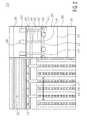
- FIG. 2 schematically illustrates a top view of part of a clamp with normal LIL connectors and a cross-sectional view taken along the lines A-A of an embodiment.
- a PNP clamp 200 of a BCD semiconductor device is formed on a substrate region 210.
- An active region 240 such as an epitaxial layer is formed above the substrate 210 and a buried insulator layer 220 is formed between the active region 240 and the substrate 210.
- the active region 240 may be doped of a first conductivity type or a second conductivity type and have a base region formed therein (not illustrated) to act as a base of the PNP ESD device.
- Emitter regions 250 and collector regions 230 are respectively formed of a conductivity type opposite to that of the base regions and are formed at the top surface of the active region 240.
- An emitter contact layer 255 and a collector contact layer 235 may be doped to be highly conductive to facilitate greater conductivity between the current carriers moving through the active region 240.
- the collector regions 230 and collector contact regions 235 are formed to have a larger area than the emitter regions 250 and emitter contact regions 255. The larger collector regions 230 allow the current carriers moving from the base to the collector to be accumulated and discharged.
- Emitter regions 250 and collector regions 230 are separated by shallow trench isolation (STI) regions 245 or walls that are formed in the active region 240.
- STI shallow trench isolation
- LOC local oxidation of silicon
- the STI regions 245 may function to clearly define the transistor regions to allow current to properly flow from emitter to base to collector, and avoid unwanted migration of charge carriers.
- a plurality of passivation layers 295 are formed atop the active region 240 in order to provide support for various metallizations and back-end processing of the device.
- Metallization and interconnection to peripheral circuitry may be implemented in the region 225. Interconnections may be made to base connections 215, collector connections 285 and emitter connections 280.
- An interconnect level above the active region 240 may, for example, include a local interconnect layer ("LIL") of the integrated circuit.
- LIL is a processing step that may be used for making trace-like connections between contact layers 270 and 275 and a semiconductor substrate 200.
- LILs 260 and 265 are formed to have a length, width and height LIL 265 creates a contact area 290 between the collector region 230.
- the LIL is provided as part of back end of line processing. Because the use of metal is prohibited during front end of line of processing, an example embodiment allows the formation of a metal Schottky contact, using standard processing as is known in the art, in which a standard LIL metallization process can be employed to provide the metal contacts to the collector 230 and the emitter 250.
- LILs 260 are formed to be at least the same length and width as contact layers 270.
- Metallization layers 280 and 285 may be formed above the contact layers 270 to connect underlying circuitry to external devices.
- thermal handling may affect the operation of the device. Viewing the cross-section of the active regions 240, the junction to be broken down during ESD stress events in the collector regions 230 is enclosed between the STI walls 245, so heat may only be released upwards and downwards, and in the length direction of the PNP 200 (i.e., in and out of the page of the cross-sectional view). As a result, thermal build-up is confined between the two STI walls. Without a way to dissipate heat upwards through the LIL 260 and other layers, only downward dissipation is possible because the passivation layers 295 and STI regions 245 do not readily conduct heat.
- FIG. 3 schematically illustrates a top view of part of an ESD clamp 300 of a BCD semiconductor device with long LIL cooling fins 365 and a cross-sectional view of the embodiment.
- the method of manufacturing the components and layers of the PNP ESD clamps 200 and 300 described herein may be formed according to well-known semiconductor processing techniques.
- Factors determining the robustness of an ESD protection device are determined by the maximum amount of current that may be handled by the device as well as heat that may be dissipated. By applying longer strips of LIL on the collector than have been previously implemented, which may be described as cooling fins, device robustness and reliability can be increased by greater than 10%. Also, by using a long LIL fin 365, the silicon footprint can be reduced by 10%, while maintaining the same device robustness. Thus, an additional structure can be provided to better dissipate heat and allow current to flow in a PNP transistor to improve the device performance thereof during an ESD event, as is described herein.
- the PNP ESD integrated circuit clamp 300 includes a substrate 310, a buried insulator layer 320 formed in the substrate, an epitaxial layer doped with a first or second conductivity type defining an active region 340 having a first top surface and a second bottom surface, with the second surface in contact with the buried insulator layer 320.
- the active region 340 may include a base well region of a second conductivity type (not illustrated).
- a plurality of collector regions 330 of a first conductivity type are formed within the active region 340 and in contact with the base region (not illustrated).
- a plurality of emitter regions 350 of the first conductivity type are formed within the active region 340 and in contact with the base region (not illustrated).
- the plurality of collector regions 330 and plurality of emitter regions 350 may be disposed in an alternating fashion within the active region 340. In this manner, a large and efficient area can be created.
- the emitter regions 350 are shorted to the base regions to enhance the speed of current flow from emitter to collector in the case of an ESD event. Current in the PNP transistor 300 flows in a horizontal direction from emitter regions to collector regions 330 as illustrated in FIG. 3 .
- the distances, or pitch, sizes between the collector regions 330, emitter 350 regions and base regions can be optimized in order to obtain maximum performance, on resistance and/or trigger voltage of the PNP ESD device.
- a plurality of passivation layers 395 are formed atop the active region 340 in order to provide support for various metallizations and back-end processing of the device.
- Metallization and interconnection to peripheral circuitry may be implemented in the region 325. Interconnections may be made to base connections 315, collector connections 385 and emitter connections 380.
- a LIL 360 is formed to have a length, width and height, creating a small contact area 390 with the emitter regions 350 within the active region 340.
- LIL 360 is formed on the first surface of the active region atop the emitter regions 350 in contact with highly doped emitter contact regions 355, where the LIL 360 is formed to have a first length. Formation and use of the highly doped emitter contact regions 355 may or may not be used.
- a LIL cooling "fin” or strip 365 may be formed atop highly doped collector contacts 335. Formation and use of the high doped collector contacts 335 may or may not be used.
- the LIL cooling fin is formed to have the same height and width of the LIL 360, and a longer length. The structure is being called a "fin” because it acts like various heat sink "fins” that are known in related arts to dissipate heat and improve performance of a given device.
- the LIL layer 360 along with LIL cooling fins 365 may be formed by known processes, such as photo-masking and etching, or by various deposition techniques as are known in the art.
- the LIL layer 360 and the collector cooling fin 365 may be made of tungsten, copper, aluminum, a combination of copper and aluminum, or of other interconnect materials as are known in the art.
- the LIL is a lowest metal interconnect level of the PNP ESD device 300.
- the LIL cooling fins 365 may be formed as Schottky contacts, directly contacting the semiconductor collector contact regions 335.
- the length of the cooling fins 365 may be formed to be substantially as long as the collector regions 330 in the direction of current flow.
- the length of the LIL cooling fin 365 may be as long as standard processing parameters allow.
- Shallow trench isolation (STI) regions 345 are formed between the emitter regions 350 and the collector regions 330 to isolate individual PNP transistors and allow the current to flow more readily in case of an ESD event.
- the LIL cooling fins 365 create an interface 390 between the LIL layer 365 and collector contact region 335 that is five to six times the size of the interface 290 of FIG. 2 .
- This larger interface 390 allows greater current and heat to flow through collector region 330 and collector contact region 335 than in previous embodiments.
- the LIL fins 365 are longer than the standard LIL layers, such as the LIL 355 formed atop the emitter regions, a greater amount of current and heat that is drawn into the collector region 330 may pass through the PNP ESD devices 300. Experiments were conducted with long LIL fins over the smaller emitter regions 350, but no additional performance gain was obtained by forming the LIL fins in the emitter regions 350.
- the use of the cooling fin reduces the silicon footprint by 10% or improves the device performance by 10% over PNP ESD devices such as the device 200 illustrated in FIG. 2 that do not use the cooling fin in the collector region.
- Table 1 - Measurement data illustrating the increase performance Reference LIL enhancement Change Turn on trigger voltage vt1 10.8V 10.8V 0% Current handling capability 1.77 mA/ ⁇ m 1.98 mA/ ⁇ m +12% On resistance 2050 ⁇ * ⁇ m 1875 ⁇ * ⁇ m -10%
- the width of an LIL cooling fin 365 is equal to a width of contact hole that is formed atop the LIL fin 365.
- the length of the LIL fin 365 is formed to be as long as processing parameters will allow the LIL fin 365 to extend the length of the collector region.
- the length of the LIL fin 365 could thus be formed to be over 50% including up to 80% or 90% or more of the length of the collector regions 330.
- Embodiments described herein may maximize the length of the LIL fin 365 to a highest percentage that the technology's design rules will allow to get as much LIL cooling fin 365 length within the collector region perimeter. This is dependent on the specific technology's design rule manual.
- the contact hole for a tungsten (W) plug 370 may be formed of a square.
- the width of the LIL cooling fin 365 may be the same as the contact plug 370.
- At least one contact hole connects to a LIL cooling fin.
- LIL connections and fins 365 may be drawn explicitly.
- a mask manipulation takes place where a physical LIL mask is generated by connecting LIL with a contact hole. Anywhere a contact hole is drawn, an LIL contact 370 or fin 365 is placed.
- Metallization layers 380 and 385 may be formed above the contact layers 370 and 375 to connect underlying circuitry to external devices.
- embodiments described herein may also be just as effective using NPN transistors.
- embodiments described herein are illustrated and described using a buried insulator layer 320, the properties exemplified by the novel long LIL cooling fin 365 structure are applicable to non-SOI substrates. The benefits of using the LIL cooling fin 365 would also accrue to a Si substrate that does not have the interspersed buried insulator layer.
Landscapes
- Semiconductor Integrated Circuits (AREA)
Abstract
Description
- Various embodiments disclosed herein relate generally to a BCD PNP transistor used for ESD protection and a method of manufacturing the same. The BCD PNP transistor uses interconnect cooling fins to reduce on-resistance, reduce the silicon footprint, and increase robustness, thus enhancing the performance of products that use the technology.
- Bipolar-CMOS-DMOS ("BCD") technology is a group of silicon processes. Each of the processes has a strength that can be combined with the strengths of the other processes on a single chip. Bipolar technology is useful for precise analog functions. Complementary Metal Oxide Semiconductor ("CMOS") is useful for digital design, and Diffused Metal Oxide Semiconductor ("DMOS") is useful for high-voltage and power applications. This combination of technologies offers many advantages such as improved reliability, reduced electromagnetic interference and smaller chip area for active components. BCD is widely used in a variety of products. The integration of BCD into Silicon-on-Insulator ("SOI") buried insulator substrates adds greater stability and is used, for example, in electromechanical, automotive safety, and audio environments.
- A brief summary of various embodiments is presented below. Some simplifications and omissions may be made in the following summary, which is intended to highlight and introduce some aspects of the various embodiments, but not to limit the scope of the embodiments described herein. Detailed descriptions of embodiments adequate to allow those of ordinary skill in the art to make and use the inventive concepts will follow in later sections.
- The embodiments described herein seek to provide an integrated circuit to improve upon device characteristics of a PNP ESD device.
- According to one embodiment, there is provided an integrated circuit including a substrate, an active region formed within the substrate, a plurality of collector regions formed within the active region, a plurality of emitter regions formed within the active region, and a local interconnect layer (LIL) contacting the plurality of emitter regions and the plurality of collector regions, the LIL including cooling fin contacts formed on the collector regions to enhance the current handling capacity of the collector regions.
- The emitter regions and collector regions may be formed in an alternating manner in a direction of current flow. A length of the cooling fins may be formed to be substantially as long as the collector regions in the direction of current flow.
- A length of the cooling fins may encompass 80% of a length of the collector regions. A length of the cooling fins may encompass a maximum length that design rules will allow.
- The integrated circuit may include shallow trench isolation (STI) regions formed to surround at least one emitter region and collector region.
- The integrated circuit may include an LIL contact formed on the active region on the emitter regions, the LIL contact having a length smaller than the length LIL cooling fin contact.
- The integrated circuit may be a BCD semiconductor device.
- The LIL layer may include tungsten, copper, aluminum, or a combination of copper and aluminum. The LIL may be a lowest metal interconnect level of the substrate.
- The integrated circuit may include a SOI buried insulating layer formed within the substrate below the emitter regions and collector regions.
- The length of the LIL cooling fin is as long as the processing parameters allows.
- According to a further embodiment, there is provided an electrostatic discharge device, including a substrate, an active region formed within the substrate, the active region including at least one base region, a plurality of collector regions disposed within the active region, a plurality of emitter regions disposed within the active region, a plurality of local interconnect layer (LIL) contacts having a first lengths and contacting the plurality of emitter regions, a plurality of LIL cooling fins having second lengths and contacting the plurality of collector regions, the second lengths being larger than the first lengths and formed to decrease the on-resistance of the electrostatic discharge device.
- The LIL cooling fins may have the same widths and heights as the LIL contacts.
- Single emitter regions and single collector regions are disposed in an alternating manner in a direction of current flow. Shallow trench isolation regions may be formed between the single emitter regions and single collector regions.
- According to a further embodiment there is provided a method of manufacturing an integrated circuit, including forming a semiconductor substrate, forming an active region within the substrate, the active region including at least one base region, forming a plurality of collector regions within the active region, forming a plurality of emitter regions within the active region, and forming a local interconnect layer (LIL) contacting the plurality of emitter regions and the plurality of collector regions, the LIL including cooling fin contacts on the collector regions to enhance the current handling capacity of the collector regions.
- The cooling fins may be substantially as long as the collector regions in the direction of current flow. A length of the cooling fins may encompass may encompass a maximum length that design rules will allow.
- The method may include forming a second LIL contact on the emitter regions, the second LIL contact having a length smaller than the length of the LIL cooling fin contact.
- Exemplary embodiments of the embodiments described herein are described in more detail and by way of non-limiting examples with reference to the accompanying drawings, wherein:
-
FIG. 1 schematically illustrates a circuit diagram of an ESD protection scheme for a CAN bus output in accordance with an embodiment; -
FIG. 2 schematically illustrates a top view of part of an ESD clamp with LIL connectors and a cross-sectional view of the embodiment; and -
FIG. 3 schematically illustrates a top view of part of an ESD clamp with long LIL cooling fins and a cross-sectional view of the embodiment. - It should be understood that the Figures are merely schematic and are not drawn to scale. It should also be understood that the same reference numerals are used throughout the Figures to indicate the same or similar parts.
- The descriptions and drawings illustrate the principles of the embodiments described herein. It will thus be appreciated that those skilled in the art will be able to devise various arrangements that, although not explicitly described or shown herein, embody the principles of the embodiments described herein and are included within its scope. Furthermore, all examples recited herein are principally intended expressly to be for pedagogical purposes to aid the reader in understanding the principles of the embodiments described herein and the concepts contributed by the inventor(s) to furthering the art, and are to be construed as being without limitation to such specifically recited examples and conditions. Additionally, the term, "or," as used herein, refers to a non-exclusive or (i.e., and/or), unless otherwise indicated (e.g., "or else" or "or in the alternative"). Also, the various embodiments described herein are not necessarily mutually exclusive, as some embodiments can be combined with one or more other embodiments to form new embodiments. As used herein, the terms "context" and "context object" will be understood to be synonymous, unless otherwise indicated.
- For every semiconductor product, an Electrostatic Discharge ("ESD") protection strategy may be provided to prevent early failures because of ESD damage. In this technology the usage of PNP bipolar transistors together with diodes is common. Other protection devices include, but are not limited to, diode chains, snapback devices and edge triggered devices.
-
FIG. 1 illustrates a circuit diagram of an ESD protection scheme for a CAN bus output in accordance with an embodiment.FIG. 1 illustrates an ESD protection scheme for a Controller Area Network ("CAN") bus output, with a stack of seven series-connected PNP transistors. CAN is a vehicle bus standard designed to allow microcontrollers and devices to communicate with each other within a vehicle without a host computer. -
FIG. 1 illustrates the importance of having the size of ESD clamps as constrained as possible. The seven PNP transistors connected in series make up an ESD clamp. Each PNP transistor can have a width of about 3,000 µm, equating to a total width of 21 mm, which is large amount of silicon area used. - The ESD clamp is constructed in such way that the turn-on voltage, as well as on-resistance and the current handling capability are tuned towards the device layout. Generally speaking, such a configuration of devices requires a considerable amount of silicon footprint.
- As result it is desirable to have an ESD structure and method that can increase device performance while not adding process steps, and does not consume additional silicon real estate.
-
FIG. 2 schematically illustrates a top view of part of a clamp with normal LIL connectors and a cross-sectional view taken along the lines A-A of an embodiment. - In the cross sectional view of
FIG. 2 aPNP clamp 200 of a BCD semiconductor device is formed on asubstrate region 210. Anactive region 240 such as an epitaxial layer is formed above thesubstrate 210 and a buriedinsulator layer 220 is formed between theactive region 240 and thesubstrate 210. Theactive region 240 may be doped of a first conductivity type or a second conductivity type and have a base region formed therein (not illustrated) to act as a base of the PNP ESD device. -
Emitter regions 250 andcollector regions 230 are respectively formed of a conductivity type opposite to that of the base regions and are formed at the top surface of theactive region 240. Anemitter contact layer 255 and acollector contact layer 235 may be doped to be highly conductive to facilitate greater conductivity between the current carriers moving through theactive region 240. Thecollector regions 230 andcollector contact regions 235 are formed to have a larger area than theemitter regions 250 andemitter contact regions 255. Thelarger collector regions 230 allow the current carriers moving from the base to the collector to be accumulated and discharged. -
Emitter regions 250 andcollector regions 230 are separated by shallow trench isolation (STI)regions 245 or walls that are formed in theactive region 240. STI or compatible isolation regions such a local oxidation of silicon (LOCOS) may be used. TheSTI regions 245 may function to clearly define the transistor regions to allow current to properly flow from emitter to base to collector, and avoid unwanted migration of charge carriers. - As illustrated in
FIG. 2 , a plurality ofpassivation layers 295 are formed atop theactive region 240 in order to provide support for various metallizations and back-end processing of the device. Metallization and interconnection to peripheral circuitry may be implemented in theregion 225. Interconnections may be made tobase connections 215,collector connections 285 andemitter connections 280. An interconnect level above theactive region 240 may, for example, include a local interconnect layer ("LIL") of the integrated circuit. LIL is a processing step that may be used for making trace-like connections betweencontact layers semiconductor substrate 200. As illustrated inFIG. 2 ,LILs height LIL 265 creates acontact area 290 between thecollector region 230. - The LIL is provided as part of back end of line processing. Because the use of metal is prohibited during front end of line of processing, an example embodiment allows the formation of a metal Schottky contact, using standard processing as is known in the art, in which a standard LIL metallization process can be employed to provide the metal contacts to the
collector 230 and theemitter 250. - As illustrated in
FIG. 2 ,LILs 260 are formed to be at least the same length and width as contact layers 270. Metallization layers 280 and 285 may be formed above the contact layers 270 to connect underlying circuitry to external devices. - During electrostatic discharge, thermal handling may affect the operation of the device. Viewing the cross-section of the
active regions 240, the junction to be broken down during ESD stress events in thecollector regions 230 is enclosed between theSTI walls 245, so heat may only be released upwards and downwards, and in the length direction of the PNP 200 (i.e., in and out of the page of the cross-sectional view). As a result, thermal build-up is confined between the two STI walls. Without a way to dissipate heat upwards through theLIL 260 and other layers, only downward dissipation is possible because the passivation layers 295 andSTI regions 245 do not readily conduct heat. -
FIG. 3 schematically illustrates a top view of part of anESD clamp 300 of a BCD semiconductor device with longLIL cooling fins 365 and a cross-sectional view of the embodiment. The method of manufacturing the components and layers of the PNP ESD clamps 200 and 300 described herein may be formed according to well-known semiconductor processing techniques. - Factors determining the robustness of an ESD protection device are determined by the maximum amount of current that may be handled by the device as well as heat that may be dissipated. By applying longer strips of LIL on the collector than have been previously implemented, which may be described as cooling fins, device robustness and reliability can be increased by greater than 10%. Also, by using a
long LIL fin 365, the silicon footprint can be reduced by 10%, while maintaining the same device robustness. Thus, an additional structure can be provided to better dissipate heat and allow current to flow in a PNP transistor to improve the device performance thereof during an ESD event, as is described herein. - As illustrated in
FIG. 3 , the PNP ESDintegrated circuit clamp 300 includes asubstrate 310, a buriedinsulator layer 320 formed in the substrate, an epitaxial layer doped with a first or second conductivity type defining anactive region 340 having a first top surface and a second bottom surface, with the second surface in contact with the buriedinsulator layer 320. Theactive region 340 may include a base well region of a second conductivity type (not illustrated). - A plurality of
collector regions 330 of a first conductivity type are formed within theactive region 340 and in contact with the base region (not illustrated). A plurality ofemitter regions 350 of the first conductivity type are formed within theactive region 340 and in contact with the base region (not illustrated). As illustrated inFIG. 3 , the plurality ofcollector regions 330 and plurality ofemitter regions 350 may be disposed in an alternating fashion within theactive region 340. In this manner, a large and efficient area can be created. In an embodiment of thePNP ESD device 300, theemitter regions 350 are shorted to the base regions to enhance the speed of current flow from emitter to collector in the case of an ESD event. Current in thePNP transistor 300 flows in a horizontal direction from emitter regions tocollector regions 330 as illustrated inFIG. 3 . - The distances, or pitch, sizes between the
collector regions 330,emitter 350 regions and base regions (not illustrated) can be optimized in order to obtain maximum performance, on resistance and/or trigger voltage of the PNP ESD device. - As illustrated in
FIG. 3 , a plurality ofpassivation layers 395 are formed atop theactive region 340 in order to provide support for various metallizations and back-end processing of the device. Metallization and interconnection to peripheral circuitry may be implemented in theregion 325. Interconnections may be made tobase connections 315,collector connections 385 andemitter connections 380. During the processing step of forming the LIL layer, aLIL 360 is formed to have a length, width and height, creating asmall contact area 390 with theemitter regions 350 within theactive region 340.LIL 360 is formed on the first surface of the active region atop theemitter regions 350 in contact with highly dopedemitter contact regions 355, where theLIL 360 is formed to have a first length. Formation and use of the highly dopedemitter contact regions 355 may or may not be used. - In addition to the
LIL 360, a LIL cooling "fin" orstrip 365 may be formed atop highly dopedcollector contacts 335. Formation and use of the highdoped collector contacts 335 may or may not be used. The LIL cooling fin is formed to have the same height and width of theLIL 360, and a longer length. The structure is being called a "fin" because it acts like various heat sink "fins" that are known in related arts to dissipate heat and improve performance of a given device. TheLIL layer 360 along withLIL cooling fins 365 may be formed by known processes, such as photo-masking and etching, or by various deposition techniques as are known in the art. - The
LIL layer 360 and thecollector cooling fin 365 may be made of tungsten, copper, aluminum, a combination of copper and aluminum, or of other interconnect materials as are known in the art. The LIL is a lowest metal interconnect level of thePNP ESD device 300. - The long
LIL cooling fins 365 formed on the first surface of theactive region 340 atop thecollector regions 330 enhance the current handling capacity of thecollector regions 330. TheLIL cooling fins 365 may be formed as Schottky contacts, directly contacting the semiconductorcollector contact regions 335. The length of the coolingfins 365 may be formed to be substantially as long as thecollector regions 330 in the direction of current flow. The length of theLIL cooling fin 365 may be as long as standard processing parameters allow. - Shallow trench isolation (STI)
regions 345 are formed between theemitter regions 350 and thecollector regions 330 to isolate individual PNP transistors and allow the current to flow more readily in case of an ESD event. - As illustrated and described, the
LIL cooling fins 365 create aninterface 390 between theLIL layer 365 andcollector contact region 335 that is five to six times the size of theinterface 290 ofFIG. 2 . Thislarger interface 390 allows greater current and heat to flow throughcollector region 330 andcollector contact region 335 than in previous embodiments. - Because the
LIL fins 365 are longer than the standard LIL layers, such as theLIL 355 formed atop the emitter regions, a greater amount of current and heat that is drawn into thecollector region 330 may pass through thePNP ESD devices 300. Experiments were conducted with long LIL fins over thesmaller emitter regions 350, but no additional performance gain was obtained by forming the LIL fins in theemitter regions 350. - Advantages of using the
LIL cooling fins 365 in thecollector regions 330 are summarized in Table 1. While the turn on voltage vt1 remained constant with the addition of using theLIL cooling fin 330, a significant increase in device characteristics has been determined. The current handling capability, or robustness of anESD PNP 300 has increased over 12% in comparison to thePNP 200 illustrated inFIG. 2 by using the longest possible cooling fin in relation to the size of a collector region, which also relates to the performance increase of the device. Also, because of thelong fin 365, the on-resistance of the device was measured to decrease on the order of 10%. Taken as a whole, the use of the cooling fin reduces the silicon footprint by 10% or improves the device performance by 10% over PNP ESD devices such as thedevice 200 illustrated inFIG. 2 that do not use the cooling fin in the collector region.Table 1 - Measurement data illustrating the increase performance Reference LIL enhancement Change Turn on trigger voltage vt1 10.8V 10.8V 0% Current handling capability 1.77 mA/µm 1.98 mA/µm +12% On resistance 2050 Ω* µm 1875 Ω* µm -10% - Additional features of the
PNP ESD device 300 will be described. The width of anLIL cooling fin 365 is equal to a width of contact hole that is formed atop theLIL fin 365. The length of theLIL fin 365 is formed to be as long as processing parameters will allow theLIL fin 365 to extend the length of the collector region. The length of theLIL fin 365 could thus be formed to be over 50% including up to 80% or 90% or more of the length of thecollector regions 330. Embodiments described herein may maximize the length of theLIL fin 365 to a highest percentage that the technology's design rules will allow to get as muchLIL cooling fin 365 length within the collector region perimeter. This is dependent on the specific technology's design rule manual. - According to standard design processes, the contact hole for a tungsten (W) plug 370 may be formed of a square. The width of the
LIL cooling fin 365 may be the same as thecontact plug 370. At least one contact hole connects to a LIL cooling fin. In the design technology used, LIL connections andfins 365 may be drawn explicitly. After finalization of a design, a mask manipulation takes place where a physical LIL mask is generated by connecting LIL with a contact hole. Anywhere a contact hole is drawn, anLIL contact 370 orfin 365 is placed. Metallization layers 380 and 385 may be formed above the contact layers 370 and 375 to connect underlying circuitry to external devices. - For any ESD clamp device, one will place the
contacts - Though embodiments related to the use of PNP transistors have been described herein, embodiments described herein may also be just as effective using NPN transistors. Although embodiments described herein are illustrated and described using a buried
insulator layer 320, the properties exemplified by the novel longLIL cooling fin 365 structure are applicable to non-SOI substrates. The benefits of using theLIL cooling fin 365 would also accrue to a Si substrate that does not have the interspersed buried insulator layer. - It should be noted that the above-mentioned embodiments illustrate rather than limit the embodiments described herein, and that those skilled in the art will be able to design many alternative embodiments without departing from the scope of the appended claims. In the claims, any reference signs placed between parentheses shall not be construed as limiting the claim. The word "comprising" does not exclude the presence of elements or steps other than those listed in a claim. The word "a" or "an" preceding an element does not exclude the presence of a plurality of such elements. The embodiments described herein can be implemented by means of hardware including several distinct elements. In the device claim enumerating several means, several of these means can be embodied by one and the same item of hardware. The mere fact that certain measures are recited in mutually different dependent claims does not indicate that a combination of these measures cannot be used to advantage.
Claims (15)
- An integrated circuit, comprising:a substrate;an active region formed within the substrate;a plurality of collector regions formed within the active region;a plurality of emitter regions formed within the active region; anda local interconnect layer (LIL) contacting the plurality of emitter regions and the plurality of collector regions, the LIL including cooling fin contacts formed on the collector regions to enhance the current handling capacity of the collector regions.
- The integrated circuit of claim 1, wherein the emitter regions and collector regions are formed in an alternating manner in a direction of current flow.
- The integrated circuit of claim 1, wherein a length of the cooling fins are formed to be substantially as long as the collector regions in the direction of current flow.
- The integrated circuit of claim 1, wherein a length of the cooling fins encompasses 80% of a length of the collector regions.
- The integrated circuit of claim 1, wherein a length of the cooling fins encompasses a maximum length that design rules will allow.
- The integrated circuit of claim 1, comprising:shallow trench isolation (STI) regions formed to surround at least one emitter region and collector region.
- The integrated circuit of claim 1, comprising:an LIL contact formed on the active region on the emitter regions, the LIL contact having a length smaller than the length LIL cooling fin contact.
- The integrated circuit of claim 1, wherein the integrated circuit is a BCD semiconductor device.
- The integrated circuit of claim 1, where the LIL layer comprises tungsten, copper, aluminum, or a combination of copper and aluminum.
- The integrated circuit of claim 1, wherein the LIL is a lowest metal interconnect level of the substrate.
- The integrated circuit of claim 1, comprising a SOI buried insulating layer formed within the substrate below the emitter regions and collector regions.
- The integrated circuit of claim 1, wherein the length of the LIL cooling fin is as long as the processing parameters allows.
- A method of manufacturing an integrated circuit, comprising:forming a semiconductor substrate;forming an active region within the substrate, the active region including at least one base region;forming a plurality of collector regions within the active region;forming a plurality of emitter regions within the active region; andforming a local interconnect layer (LIL) contacting the plurality of emitter regions and the plurality of collector regions, the LIL including cooling fin contacts on the collector regions to enhance the current handling capacity of the collector regions.
- The method of claim 13, comprising:forming the cooling fins to be substantially as long as the collector regions in the direction of current flow.
- The method of claim 13, wherein a length of the cooling fins encompasses a maximum length that design rules will allow.
Applications Claiming Priority (1)
| Application Number | Priority Date | Filing Date | Title |
|---|---|---|---|
| US14/495,468 US9653447B2 (en) | 2014-09-24 | 2014-09-24 | Local interconnect layer enhanced ESD in a bipolar-CMOS-DMOS |
Publications (2)
| Publication Number | Publication Date |
|---|---|
| EP3001457A1 true EP3001457A1 (en) | 2016-03-30 |
| EP3001457B1 EP3001457B1 (en) | 2022-02-23 |
Family
ID=54198976
Family Applications (1)
| Application Number | Title | Priority Date | Filing Date |
|---|---|---|---|
| EP15186224.0A Active EP3001457B1 (en) | 2014-09-24 | 2015-09-22 | Lil enhanced esd-pnp in a bcd |
Country Status (3)
| Country | Link |
|---|---|
| US (1) | US9653447B2 (en) |
| EP (1) | EP3001457B1 (en) |
| CN (1) | CN105448907B (en) |
Cited By (3)
| Publication number | Priority date | Publication date | Assignee | Title |
|---|---|---|---|---|
| EP3367436A1 (en) * | 2017-02-24 | 2018-08-29 | Nxp B.V. | Electrostatic discharge (esd) protection device and method for operating an esd protection device |
| EP3382757A1 (en) * | 2017-03-28 | 2018-10-03 | Nxp B.V. | Electrostatic discharge (esd) protection device and method for operating an esd protection device |
| EP4016611A1 (en) * | 2020-12-21 | 2022-06-22 | Nxp B.V. | Metal oxide semicondutor device and method of construction therefor |
Families Citing this family (3)
| Publication number | Priority date | Publication date | Assignee | Title |
|---|---|---|---|---|
| CN108305873B (en) * | 2017-01-12 | 2021-01-29 | 中芯国际集成电路制造(上海)有限公司 | Electrostatic discharge clamping device and electrostatic discharge clamping circuit |
| US10784257B2 (en) * | 2018-08-31 | 2020-09-22 | Nxp B.V. | Integrating silicon-BJT to a silicon-germanium-HBT manufacturing process |
| JP7545298B2 (en) * | 2020-11-13 | 2024-09-04 | 株式会社日立製作所 | Power Conversion Equipment |
Citations (5)
| Publication number | Priority date | Publication date | Assignee | Title |
|---|---|---|---|---|
| US5436475A (en) * | 1990-09-20 | 1995-07-25 | Siemens Aktiengesellschaft | Bipolar transistor for high power in the microwave range |
| US6566733B1 (en) * | 2002-06-19 | 2003-05-20 | Micrel, Inc. | Method and system for providing a power lateral PNP transistor using a buried power buss |
| US6777784B1 (en) * | 2000-10-17 | 2004-08-17 | National Semiconductor Corporation | Bipolar transistor-based electrostatic discharge (ESD) protection structure with a heat sink |
| WO2005001930A1 (en) * | 2003-06-27 | 2005-01-06 | Koninklijke Philips Electronics N.V. | Integrated circuit with an integrated heat sink |
| WO2005052997A2 (en) * | 2003-11-21 | 2005-06-09 | Wisconsin Alumni Resarch Foundation | Solid-state high power device and method |
Family Cites Families (10)
| Publication number | Priority date | Publication date | Assignee | Title |
|---|---|---|---|---|
| US4721682A (en) * | 1985-09-25 | 1988-01-26 | Monolithic Memories, Inc. | Isolation and substrate connection for a bipolar integrated circuit |
| US4760433A (en) * | 1986-01-31 | 1988-07-26 | Harris Corporation | ESD protection transistors |
| US5504362A (en) * | 1992-12-22 | 1996-04-02 | International Business Machines Corporation | Electrostatic discharge protection device |
| US7238565B2 (en) * | 2004-12-08 | 2007-07-03 | International Business Machines Corporation | Methodology for recovery of hot carrier induced degradation in bipolar devices |
| US8866263B2 (en) * | 2006-09-26 | 2014-10-21 | Texas Instruments Incorporated | Emitter ballasting by contact area segmentation in ESD bipolar based semiconductor component |
| KR100832716B1 (en) * | 2006-12-27 | 2008-05-28 | 동부일렉트로닉스 주식회사 | Bipolar Transistors and Manufacturing Method Thereof |
| US8553380B2 (en) * | 2010-07-08 | 2013-10-08 | Analog Devices, Inc. | Apparatus and method for electronic circuit protection |
| US8848325B2 (en) * | 2012-02-21 | 2014-09-30 | Macronix International Co., Ltd. | High voltage semiconductor element and operating method thereof |
| US9224724B2 (en) * | 2012-05-30 | 2015-12-29 | Texas Instruments Incorporated | Mutual ballasting multi-finger bidirectional ESD device |
| US9214542B2 (en) * | 2013-03-11 | 2015-12-15 | Freescale Semiconductor, Inc. | Semiconductor device with integrated electrostatic discharge (ESD) clamp |
-
2014
- 2014-09-24 US US14/495,468 patent/US9653447B2/en active Active
-
2015
- 2015-09-16 CN CN201510589960.0A patent/CN105448907B/en active Active
- 2015-09-22 EP EP15186224.0A patent/EP3001457B1/en active Active
Patent Citations (5)
| Publication number | Priority date | Publication date | Assignee | Title |
|---|---|---|---|---|
| US5436475A (en) * | 1990-09-20 | 1995-07-25 | Siemens Aktiengesellschaft | Bipolar transistor for high power in the microwave range |
| US6777784B1 (en) * | 2000-10-17 | 2004-08-17 | National Semiconductor Corporation | Bipolar transistor-based electrostatic discharge (ESD) protection structure with a heat sink |
| US6566733B1 (en) * | 2002-06-19 | 2003-05-20 | Micrel, Inc. | Method and system for providing a power lateral PNP transistor using a buried power buss |
| WO2005001930A1 (en) * | 2003-06-27 | 2005-01-06 | Koninklijke Philips Electronics N.V. | Integrated circuit with an integrated heat sink |
| WO2005052997A2 (en) * | 2003-11-21 | 2005-06-09 | Wisconsin Alumni Resarch Foundation | Solid-state high power device and method |
Cited By (5)
| Publication number | Priority date | Publication date | Assignee | Title |
|---|---|---|---|---|
| EP3367436A1 (en) * | 2017-02-24 | 2018-08-29 | Nxp B.V. | Electrostatic discharge (esd) protection device and method for operating an esd protection device |
| US10446539B2 (en) | 2017-02-24 | 2019-10-15 | Nxp B.V. | Electrostatic discharge (ESD) protection device and method for operating an ESD protection device |
| EP3382757A1 (en) * | 2017-03-28 | 2018-10-03 | Nxp B.V. | Electrostatic discharge (esd) protection device and method for operating an esd protection device |
| US10431578B2 (en) | 2017-03-28 | 2019-10-01 | Nxp B.V. | Electrostatic discharge (ESD) protection device and method for operating an ESD protection device |
| EP4016611A1 (en) * | 2020-12-21 | 2022-06-22 | Nxp B.V. | Metal oxide semicondutor device and method of construction therefor |
Also Published As
| Publication number | Publication date |
|---|---|
| CN105448907A (en) | 2016-03-30 |
| US20160086934A1 (en) | 2016-03-24 |
| US9653447B2 (en) | 2017-05-16 |
| CN105448907B (en) | 2019-04-05 |
| EP3001457B1 (en) | 2022-02-23 |
Similar Documents
| Publication | Publication Date | Title |
|---|---|---|
| TWI511291B (en) | Semiconductor device and method of manufacturing same | |
| EP3001457B1 (en) | Lil enhanced esd-pnp in a bcd | |
| US11031327B2 (en) | Through vias and methods of formation thereof | |
| US9653448B2 (en) | Electrostatic discharge (ESD) diode in FinFET technology | |
| CN102842576B (en) | Semiconductor device | |
| KR101352685B1 (en) | Vertical Butt and Scr for ESD | |
| US9536870B2 (en) | SCR with fin body regions for ESD protection | |
| TWI668833B (en) | Semiconductor electrostatic discharge protection device | |
| TWI704670B (en) | Semiconductor device for electrostatic discharge protection | |
| EP3021359B1 (en) | Electrostatic discharge (esd) protection device | |
| CN102790048B (en) | BJT Semiconductor Structure with Embedded Schottky Diode | |
| TWI536562B (en) | High voltage semiconductor component and method of manufacturing same | |
| US8963202B2 (en) | Electrostatic discharge protection apparatus | |
| US9722035B2 (en) | Method for manufacturing termination structure of semiconductor device | |
| CN115708209B (en) | Semiconductor electrostatic protection device | |
| CN104979340B (en) | Semiconductor structure and electrostatic discharge protection circuit | |
| US11011510B2 (en) | Breakdown uniformity for ESD protection device | |
| TWI566376B (en) | Semiconductor device and method of manufacturing same | |
| US10535583B2 (en) | Electrostatic discharge protection device and fabrication method thereof | |
| TWI680579B (en) | Transistor device | |
| CN103227171B (en) | Semiconductor structure and manufacturing method thereof | |
| CN102738141A (en) | Semiconductor structure and manufacturing method and operating method thereof | |
| JP3830871B2 (en) | Electrostatic discharge protection element | |
| CN106206565A (en) | Diode and diode string circuit | |
| CN117616572A (en) | Semiconductor device and manufacturing method thereof |
Legal Events
| Date | Code | Title | Description |
|---|---|---|---|
| PUAI | Public reference made under article 153(3) epc to a published international application that has entered the european phase |
Free format text: ORIGINAL CODE: 0009012 |
|
| AK | Designated contracting states |
Kind code of ref document: A1 Designated state(s): AL AT BE BG CH CY CZ DE DK EE ES FI FR GB GR HR HU IE IS IT LI LT LU LV MC MK MT NL NO PL PT RO RS SE SI SK SM TR |
|
| AX | Request for extension of the european patent |
Extension state: BA ME |
|
| 17P | Request for examination filed |
Effective date: 20160930 |
|
| RBV | Designated contracting states (corrected) |
Designated state(s): AL AT BE BG CH CY CZ DE DK EE ES FI FR GB GR HR HU IE IS IT LI LT LU LV MC MK MT NL NO PL PT RO RS SE SI SK SM TR |
|
| STAA | Information on the status of an ep patent application or granted ep patent |
Free format text: STATUS: EXAMINATION IS IN PROGRESS |
|
| 17Q | First examination report despatched |
Effective date: 20181102 |
|
| GRAP | Despatch of communication of intention to grant a patent |
Free format text: ORIGINAL CODE: EPIDOSNIGR1 |
|
| STAA | Information on the status of an ep patent application or granted ep patent |
Free format text: STATUS: GRANT OF PATENT IS INTENDED |
|
| INTG | Intention to grant announced |
Effective date: 20211019 |
|
| RIN1 | Information on inventor provided before grant (corrected) |
Inventor name: CLAES, JAN Inventor name: HUITSING, ALBERT JAN |
|
| GRAS | Grant fee paid |
Free format text: ORIGINAL CODE: EPIDOSNIGR3 |
|
| GRAA | (expected) grant |
Free format text: ORIGINAL CODE: 0009210 |
|
| STAA | Information on the status of an ep patent application or granted ep patent |
Free format text: STATUS: THE PATENT HAS BEEN GRANTED |
|
| AK | Designated contracting states |
Kind code of ref document: B1 Designated state(s): AL AT BE BG CH CY CZ DE DK EE ES FI FR GB GR HR HU IE IS IT LI LT LU LV MC MK MT NL NO PL PT RO RS SE SI SK SM TR |
|
| REG | Reference to a national code |
Ref country code: GB Ref legal event code: FG4D |
|
| REG | Reference to a national code |
Ref country code: CH Ref legal event code: EP |
|
| REG | Reference to a national code |
Ref country code: AT Ref legal event code: REF Ref document number: 1471108 Country of ref document: AT Kind code of ref document: T Effective date: 20220315 |
|
| REG | Reference to a national code |
Ref country code: IE Ref legal event code: FG4D |
|
| REG | Reference to a national code |
Ref country code: DE Ref legal event code: R096 Ref document number: 602015077044 Country of ref document: DE |
|
| REG | Reference to a national code |
Ref country code: LT Ref legal event code: MG9D |
|
| REG | Reference to a national code |
Ref country code: NL Ref legal event code: MP Effective date: 20220223 |
|
| REG | Reference to a national code |
Ref country code: AT Ref legal event code: MK05 Ref document number: 1471108 Country of ref document: AT Kind code of ref document: T Effective date: 20220223 |
|
| PG25 | Lapsed in a contracting state [announced via postgrant information from national office to epo] |
Ref country code: SE Free format text: LAPSE BECAUSE OF FAILURE TO SUBMIT A TRANSLATION OF THE DESCRIPTION OR TO PAY THE FEE WITHIN THE PRESCRIBED TIME-LIMIT Effective date: 20220223 Ref country code: RS Free format text: LAPSE BECAUSE OF FAILURE TO SUBMIT A TRANSLATION OF THE DESCRIPTION OR TO PAY THE FEE WITHIN THE PRESCRIBED TIME-LIMIT Effective date: 20220223 Ref country code: PT Free format text: LAPSE BECAUSE OF FAILURE TO SUBMIT A TRANSLATION OF THE DESCRIPTION OR TO PAY THE FEE WITHIN THE PRESCRIBED TIME-LIMIT Effective date: 20220623 Ref country code: NO Free format text: LAPSE BECAUSE OF FAILURE TO SUBMIT A TRANSLATION OF THE DESCRIPTION OR TO PAY THE FEE WITHIN THE PRESCRIBED TIME-LIMIT Effective date: 20220523 Ref country code: NL Free format text: LAPSE BECAUSE OF FAILURE TO SUBMIT A TRANSLATION OF THE DESCRIPTION OR TO PAY THE FEE WITHIN THE PRESCRIBED TIME-LIMIT Effective date: 20220223 Ref country code: LT Free format text: LAPSE BECAUSE OF FAILURE TO SUBMIT A TRANSLATION OF THE DESCRIPTION OR TO PAY THE FEE WITHIN THE PRESCRIBED TIME-LIMIT Effective date: 20220223 Ref country code: HR Free format text: LAPSE BECAUSE OF FAILURE TO SUBMIT A TRANSLATION OF THE DESCRIPTION OR TO PAY THE FEE WITHIN THE PRESCRIBED TIME-LIMIT Effective date: 20220223 Ref country code: ES Free format text: LAPSE BECAUSE OF FAILURE TO SUBMIT A TRANSLATION OF THE DESCRIPTION OR TO PAY THE FEE WITHIN THE PRESCRIBED TIME-LIMIT Effective date: 20220223 Ref country code: BG Free format text: LAPSE BECAUSE OF FAILURE TO SUBMIT A TRANSLATION OF THE DESCRIPTION OR TO PAY THE FEE WITHIN THE PRESCRIBED TIME-LIMIT Effective date: 20220523 |
|
| PG25 | Lapsed in a contracting state [announced via postgrant information from national office to epo] |
Ref country code: PL Free format text: LAPSE BECAUSE OF FAILURE TO SUBMIT A TRANSLATION OF THE DESCRIPTION OR TO PAY THE FEE WITHIN THE PRESCRIBED TIME-LIMIT Effective date: 20220223 Ref country code: LV Free format text: LAPSE BECAUSE OF FAILURE TO SUBMIT A TRANSLATION OF THE DESCRIPTION OR TO PAY THE FEE WITHIN THE PRESCRIBED TIME-LIMIT Effective date: 20220223 Ref country code: GR Free format text: LAPSE BECAUSE OF FAILURE TO SUBMIT A TRANSLATION OF THE DESCRIPTION OR TO PAY THE FEE WITHIN THE PRESCRIBED TIME-LIMIT Effective date: 20220524 Ref country code: FI Free format text: LAPSE BECAUSE OF FAILURE TO SUBMIT A TRANSLATION OF THE DESCRIPTION OR TO PAY THE FEE WITHIN THE PRESCRIBED TIME-LIMIT Effective date: 20220223 Ref country code: AT Free format text: LAPSE BECAUSE OF FAILURE TO SUBMIT A TRANSLATION OF THE DESCRIPTION OR TO PAY THE FEE WITHIN THE PRESCRIBED TIME-LIMIT Effective date: 20220223 |
|
| PG25 | Lapsed in a contracting state [announced via postgrant information from national office to epo] |
Ref country code: IS Free format text: LAPSE BECAUSE OF FAILURE TO SUBMIT A TRANSLATION OF THE DESCRIPTION OR TO PAY THE FEE WITHIN THE PRESCRIBED TIME-LIMIT Effective date: 20220623 |
|
| PG25 | Lapsed in a contracting state [announced via postgrant information from national office to epo] |
Ref country code: SM Free format text: LAPSE BECAUSE OF FAILURE TO SUBMIT A TRANSLATION OF THE DESCRIPTION OR TO PAY THE FEE WITHIN THE PRESCRIBED TIME-LIMIT Effective date: 20220223 Ref country code: SK Free format text: LAPSE BECAUSE OF FAILURE TO SUBMIT A TRANSLATION OF THE DESCRIPTION OR TO PAY THE FEE WITHIN THE PRESCRIBED TIME-LIMIT Effective date: 20220223 Ref country code: RO Free format text: LAPSE BECAUSE OF FAILURE TO SUBMIT A TRANSLATION OF THE DESCRIPTION OR TO PAY THE FEE WITHIN THE PRESCRIBED TIME-LIMIT Effective date: 20220223 Ref country code: EE Free format text: LAPSE BECAUSE OF FAILURE TO SUBMIT A TRANSLATION OF THE DESCRIPTION OR TO PAY THE FEE WITHIN THE PRESCRIBED TIME-LIMIT Effective date: 20220223 Ref country code: DK Free format text: LAPSE BECAUSE OF FAILURE TO SUBMIT A TRANSLATION OF THE DESCRIPTION OR TO PAY THE FEE WITHIN THE PRESCRIBED TIME-LIMIT Effective date: 20220223 Ref country code: CZ Free format text: LAPSE BECAUSE OF FAILURE TO SUBMIT A TRANSLATION OF THE DESCRIPTION OR TO PAY THE FEE WITHIN THE PRESCRIBED TIME-LIMIT Effective date: 20220223 |
|
| REG | Reference to a national code |
Ref country code: DE Ref legal event code: R097 Ref document number: 602015077044 Country of ref document: DE |
|
| PG25 | Lapsed in a contracting state [announced via postgrant information from national office to epo] |
Ref country code: AL Free format text: LAPSE BECAUSE OF FAILURE TO SUBMIT A TRANSLATION OF THE DESCRIPTION OR TO PAY THE FEE WITHIN THE PRESCRIBED TIME-LIMIT Effective date: 20220223 |
|
| PLBE | No opposition filed within time limit |
Free format text: ORIGINAL CODE: 0009261 |
|
| STAA | Information on the status of an ep patent application or granted ep patent |
Free format text: STATUS: NO OPPOSITION FILED WITHIN TIME LIMIT |
|
| 26N | No opposition filed |
Effective date: 20221124 |
|
| PG25 | Lapsed in a contracting state [announced via postgrant information from national office to epo] |
Ref country code: SI Free format text: LAPSE BECAUSE OF FAILURE TO SUBMIT A TRANSLATION OF THE DESCRIPTION OR TO PAY THE FEE WITHIN THE PRESCRIBED TIME-LIMIT Effective date: 20220223 |
|
| PG25 | Lapsed in a contracting state [announced via postgrant information from national office to epo] |
Ref country code: MC Free format text: LAPSE BECAUSE OF FAILURE TO SUBMIT A TRANSLATION OF THE DESCRIPTION OR TO PAY THE FEE WITHIN THE PRESCRIBED TIME-LIMIT Effective date: 20220223 |
|
| REG | Reference to a national code |
Ref country code: CH Ref legal event code: PL |
|
| REG | Reference to a national code |
Ref country code: BE Ref legal event code: MM Effective date: 20220930 |
|
| PG25 | Lapsed in a contracting state [announced via postgrant information from national office to epo] |
Ref country code: LU Free format text: LAPSE BECAUSE OF NON-PAYMENT OF DUE FEES Effective date: 20220922 |
|
| PG25 | Lapsed in a contracting state [announced via postgrant information from national office to epo] |
Ref country code: LI Free format text: LAPSE BECAUSE OF NON-PAYMENT OF DUE FEES Effective date: 20220930 Ref country code: IT Free format text: LAPSE BECAUSE OF FAILURE TO SUBMIT A TRANSLATION OF THE DESCRIPTION OR TO PAY THE FEE WITHIN THE PRESCRIBED TIME-LIMIT Effective date: 20220223 Ref country code: IE Free format text: LAPSE BECAUSE OF NON-PAYMENT OF DUE FEES Effective date: 20220922 Ref country code: CH Free format text: LAPSE BECAUSE OF NON-PAYMENT OF DUE FEES Effective date: 20220930 |
|
| P01 | Opt-out of the competence of the unified patent court (upc) registered |
Effective date: 20230725 |
|
| PG25 | Lapsed in a contracting state [announced via postgrant information from national office to epo] |
Ref country code: BE Free format text: LAPSE BECAUSE OF NON-PAYMENT OF DUE FEES Effective date: 20220930 |
|
| PG25 | Lapsed in a contracting state [announced via postgrant information from national office to epo] |
Ref country code: HU Free format text: LAPSE BECAUSE OF FAILURE TO SUBMIT A TRANSLATION OF THE DESCRIPTION OR TO PAY THE FEE WITHIN THE PRESCRIBED TIME-LIMIT; INVALID AB INITIO Effective date: 20150922 |
|
| PG25 | Lapsed in a contracting state [announced via postgrant information from national office to epo] |
Ref country code: CY Free format text: LAPSE BECAUSE OF FAILURE TO SUBMIT A TRANSLATION OF THE DESCRIPTION OR TO PAY THE FEE WITHIN THE PRESCRIBED TIME-LIMIT Effective date: 20220223 |
|
| PG25 | Lapsed in a contracting state [announced via postgrant information from national office to epo] |
Ref country code: MK Free format text: LAPSE BECAUSE OF FAILURE TO SUBMIT A TRANSLATION OF THE DESCRIPTION OR TO PAY THE FEE WITHIN THE PRESCRIBED TIME-LIMIT Effective date: 20220223 |
|
| PG25 | Lapsed in a contracting state [announced via postgrant information from national office to epo] |
Ref country code: MT Free format text: LAPSE BECAUSE OF FAILURE TO SUBMIT A TRANSLATION OF THE DESCRIPTION OR TO PAY THE FEE WITHIN THE PRESCRIBED TIME-LIMIT Effective date: 20220223 |
|
| PGFP | Annual fee paid to national office [announced via postgrant information from national office to epo] |
Ref country code: DE Payment date: 20240820 Year of fee payment: 10 |
|
| PGFP | Annual fee paid to national office [announced via postgrant information from national office to epo] |
Ref country code: GB Payment date: 20240820 Year of fee payment: 10 |
|
| PGFP | Annual fee paid to national office [announced via postgrant information from national office to epo] |
Ref country code: FR Payment date: 20240820 Year of fee payment: 10 |
|
| REG | Reference to a national code |
Ref country code: DE Ref legal event code: R079 Ref document number: 602015077044 Country of ref document: DE Free format text: PREVIOUS MAIN CLASS: H01L0027020000 Ipc: H10D0089000000 |
|
| PG25 | Lapsed in a contracting state [announced via postgrant information from national office to epo] |
Ref country code: TR Free format text: LAPSE BECAUSE OF FAILURE TO SUBMIT A TRANSLATION OF THE DESCRIPTION OR TO PAY THE FEE WITHIN THE PRESCRIBED TIME-LIMIT Effective date: 20220223 |