EP3001456A2 - Overvoltage protection device and method - Google Patents
Overvoltage protection device and method Download PDFInfo
- Publication number
- EP3001456A2 EP3001456A2 EP15183728.3A EP15183728A EP3001456A2 EP 3001456 A2 EP3001456 A2 EP 3001456A2 EP 15183728 A EP15183728 A EP 15183728A EP 3001456 A2 EP3001456 A2 EP 3001456A2
- Authority
- EP
- European Patent Office
- Prior art keywords
- region
- protection device
- overvoltage protection
- base
- transistor
- Prior art date
- Legal status (The legal status is an assumption and is not a legal conclusion. Google has not performed a legal analysis and makes no representation as to the accuracy of the status listed.)
- Granted
Links
Images










Classifications
-
- H—ELECTRICITY
- H10—SEMICONDUCTOR DEVICES; ELECTRIC SOLID-STATE DEVICES NOT OTHERWISE PROVIDED FOR
- H10D—INORGANIC ELECTRIC SEMICONDUCTOR DEVICES
- H10D10/00—Bipolar junction transistors [BJT]
- H10D10/60—Lateral BJTs
-
- H—ELECTRICITY
- H02—GENERATION; CONVERSION OR DISTRIBUTION OF ELECTRIC POWER
- H02H—EMERGENCY PROTECTIVE CIRCUIT ARRANGEMENTS
- H02H9/00—Emergency protective circuit arrangements for limiting excess current or voltage without disconnection
- H02H9/04—Emergency protective circuit arrangements for limiting excess current or voltage without disconnection responsive to excess voltage
- H02H9/044—Physical layout, materials not provided for elsewhere
-
- H—ELECTRICITY
- H02—GENERATION; CONVERSION OR DISTRIBUTION OF ELECTRIC POWER
- H02H—EMERGENCY PROTECTIVE CIRCUIT ARRANGEMENTS
- H02H7/00—Emergency protective circuit arrangements specially adapted for specific types of electric machines or apparatus or for sectionalised protection of cable or line systems, and effecting automatic switching in the event of an undesired change from normal working conditions
- H02H7/16—Emergency protective circuit arrangements specially adapted for specific types of electric machines or apparatus or for sectionalised protection of cable or line systems, and effecting automatic switching in the event of an undesired change from normal working conditions for capacitors
-
- H—ELECTRICITY
- H10—SEMICONDUCTOR DEVICES; ELECTRIC SOLID-STATE DEVICES NOT OTHERWISE PROVIDED FOR
- H10D—INORGANIC ELECTRIC SEMICONDUCTOR DEVICES
- H10D62/00—Semiconductor bodies, or regions thereof, of devices having potential barriers
- H10D62/10—Shapes, relative sizes or dispositions of the regions of the semiconductor bodies; Shapes of the semiconductor bodies
- H10D62/124—Shapes, relative sizes or dispositions of the regions of semiconductor bodies or of junctions between the regions
- H10D62/126—Top-view geometrical layouts of the regions or the junctions
-
- H—ELECTRICITY
- H10—SEMICONDUCTOR DEVICES; ELECTRIC SOLID-STATE DEVICES NOT OTHERWISE PROVIDED FOR
- H10D—INORGANIC ELECTRIC SEMICONDUCTOR DEVICES
- H10D89/00—Aspects of integrated devices not covered by groups H10D84/00 - H10D88/00
- H10D89/60—Integrated devices comprising arrangements for electrical or thermal protection, e.g. protection circuits against electrostatic discharge [ESD]
- H10D89/601—Integrated devices comprising arrangements for electrical or thermal protection, e.g. protection circuits against electrostatic discharge [ESD] for devices having insulated gate electrodes, e.g. for IGFETs or IGBTs
- H10D89/711—Integrated devices comprising arrangements for electrical or thermal protection, e.g. protection circuits against electrostatic discharge [ESD] for devices having insulated gate electrodes, e.g. for IGFETs or IGBTs using bipolar transistors as protective elements
Definitions
- This disclosure relates to circuits to provide other components with protection against overvoltage, such as electrostatic discharge (ESD) and/or electrical overstress (EOS) events.
- ESD electrostatic discharge
- EOS electrical overstress
- Modern electronics relies on integrated circuits where large numbers of transistors are provided within a single package. For performance, such as speed, the transistors are often designed to operate at relatively low voltages, for example, between a few volts and a few tens of volts.
- Integrated circuits are packaged to protect them, but need to connect to components outside of the package by way of legs or pins or similar structures. These may in turn connect to terminals, connectors or sockets provided on a product in which the integrated circuit is provided. Thus, even when an integrated circuit is mounted on a circuit board, it can be subjected to electrostatic shocks. It is known that integrated circuits waiting to be placed on a circuit board are especially vulnerable to electrostatic discharge or other overvoltage events.
- circuits that provide overvoltage protection.
- Simple examples are the provision of reverse biased diodes between a node to be protected and the supply rails of an integrated circuit.
- Performance of the circuits can be assessed against several published test standards.
- One such standard is the International Electrotechnical Commission (IEC) CDM (charged device model) where peak current can be in the range of 6A with a rise time of less than 400 pico-seconds. ESD events of this nature may give rise to gate oxide damage of MOSFETs, junction damage and charge trapping with integrated circuits.
- IEC International Electrotechnical Commission
- an overvoltage protection device comprising a bipolar transistor.
- the bipolar transistor has base, collector and emitter regions. The collector and emitter regions are provided adjacent one another.
- the voltage at which punch-through driven triggering of the overvoltage protection device occurs can be controlled.
- a particular distance between the collector and emitter regions can be selected to achieve a desired trigger voltage of the overvoltage protection device.
- a conductor may extend above a semiconductor between the collector and emitter regions and be electrically isolated from the semiconductor.
- the conductor can be held at a voltage, such as the emitter voltage, such that it acts as a field plate or resurf structure.
- the conductor may be used as a gate so as to form a MOSFET having a channel within the bipolar transistor.
- the overvoltage protection device may further comprise a capacitor connected between a node to be protected and the base (or base/gate) of the transistor.
- an overvoltage protection device comprising a bipolar transistor structure.
- the bipolar transistor structure has base, collector and emitter regions.
- the collector and emitter regions are in a current flow path that is connected to a node to be protected from an overvoltage event.
- the current flow path extends to a discharge path.
- the overvoltage protection device further comprises a component, such as a suitably connected capacitor or diode, to facilitate turn on of the protection device.
- a capacitor has a first terminal connected to the base terminal, and a second terminal connected to the collector and/or the node to be protected.
- the bipolar transistor structure may have a doping concentration within its various regions that makes the device asymmetric (i.e. the collector- base and base-emitter regions are different).
- a bi-directional protection device can be used to protect an integrated circuit from both a positive polarity ESD event and a negative polarity ESD event.
- capacitors may connect between the base and the collector and between the base and the emitter.
- the bipolar transistor structure may be associated with a second bipolar transistor structure to form a silicon controlled rectifier (SCR). Regions of silicon may be shared by both of the transistors.
- SCR silicon controlled rectifier
- the base of the bipolar transistor structure may be connected to a second current flow path having at least one of a resistive impedance and an inductive impedance to control base current in the transistor when the transistor is on.
- an overvoltage protection device comprising a bipolar transistor, wherein the bipolar transistor has base, collector and emitter regions.
- the collector is connected to a node to be protected and the emitter is connected to a discharge path, such as a power rail or ground supply.
- the transistor has a relatively thin base region disposed beneath (or above) the emitter region. It is thus possible to modify the structure of the bipolar transistor to make it respond more quickly. For example, implementing the bipolar transistor with a relatively thin base region can improve turn-on speed, which can aid in reducing voltage build-up during an ESD and/or EOS event.
- the overvoltage protection device comprises a bipolar transistor connected between a node to be protected and a discharge path.
- the base width of the transistor is selected such that carrier transit time across the base gives rise to a unity gain frequency (F T ) value of the transistor substantially equal to an inverse of a rise time of an ESD event.
- F T value is greater than 1GHz such that the corresponding rise time is less than one nanosecond.
- the transistor base further comprises a further base region disposed adjacent the collector, but separated therefrom.
- the further base region and the collector are separated by a region of reduced doping. The distance by which the collector and the further base region are separated controls a breakdown voltage of the device.
- an overvoltage protection device comprising a transistor or a silicon controlled rectifier in combination with at least one clamping diode.
- the clamping diodes may be provided in parallel and series to synthesize a composite diode having desirable electrical characteristics.
- the diode or composite diode may be provided in parallel with the transistor or the silicon controlled rectifier. Additionally or alternatively the clamping diodes may be connected to a control node of the transistor or silicon controlled rectifier.
- the transistor may be a bipolar transistor or a FET.
- a method of providing overvoltage protection to a node includes forming a transistor having a body of a first type of semiconductor and first and second regions of a second type of semiconductor, one of the first and second regions being connected to a node to be protected and the other of the regions being connected to a discharge path.
- the body forms a base region of the transistor and a capacitance is provided between the node to be protected and the body region to inject change to turn the transistor on;
- a layer of the first type of semiconductor is provided beneath the one of the regions that acts as an emitter of the transistor to form a bipolar transistor with a unity gain frequency of greater than 1GHz;
- at least one clamping diode extends between the first and second regions;
- the first and second regions are adjacent one another but not contiguous such that punch through occurs to indicate conduction in the transistor;
- the first and second regions are adjacent one another and separated from one another, and a gate electrode is formed between them to allow a voltage at the node to be protected in excess of a threshold voltage to cause conduction between the first and second regions along a channel;
- the base-collector interface region is enlarged by forming the base on either side of or at least partially around the region connected to the node to be protected; and/or (g) the
- US 2011-0101444 discloses an overvoltage protection device 5 based around a horizontal NPN transistor which is formed within an insulated well, although it should be understood that this disclosure is not limited to the use of such silicon-on-insulator transistors. Such a device is shown in Figure 1 .
- a layer of insulation 22 is formed over a substrate 10.
- the substrate may be a semiconductor.
- the semiconductor is silicon, but other semiconductors may also be used.
- a relatively heavily doped P+ layer 24 is provided over the layer of insulation 22 or just over part of it which in the finished device is beneath a base region B of the transistor as shown in Figure 1 .
- An epitaxial layer 30 of P type material is provided over the P+ region 24.
- the P type material of the epitaxial layer 30 forms a body of the overvoltage protection device.
- the P+ region 24 helps inhibit the formation of parasitic vertical transistors and also, being heavily doped, helps to shield the base region B and emitter region E of the device from electrostatic fields resulting from the epitaxial layer 30 being at a different potential relative to the substrate 10.
- a first N type region 40 is formed, as shown in Figure 1 , towards the left hand side of the device.
- the device 5 in this example has rotational symmetry such that the same region 40 also exists on the right hand side of the device 5. This region forms a collector C.
- a P+ region 50 is implanted to form a base region B, the P+ region 50 being implanted adjacent but spaced apart from the N type region 40.
- a further N+ region 60 that forms the emitter E is implanted within the P+ region 50.
- the collector regions 40 need only be provided in the vicinity of the surface.
- the N + region 40 can be extended by forming region 40a, or regions 40a and 40b, as illustrated. It will be appreciated that as the device may be formed by growing an epitaxial layer over an initial (handle) wafer, then region 40b may be implanted, or otherwise doped, before the layer containing region 40a is grown on the wafer. Similarly, region 40a may be implanted with dopant before a top layer containing region 40 is grown on the wafer or it can be done at the same time.
- the regions 40 and 60 are doped to a similar concentration such that either can function as a collector or as an emitter of the lateral NPN transistor.
- the transistor may be fabricated such that it has one region where performance is enhanced when that region is used as the emitter.
- the N type regions 40 and 60 are doped to around 10 16 donor impurities per cubic centimeter whilst the epitaxial layer 30 associated with the P type body is more lightly doped at around 10 15 acceptor impurities per cubic centimeter.
- Such a device triggers automatically as the voltage across it increases.
- the trigger mechanism is provided and controlled by controlling the lateral extent of a distance D between the edge of the collector region and the edge of the base region to adjust the trigger voltage, and distance L representing the width of the base region to adjust the holding voltage.
- the distances D and L can be selected at production by the use of mask positioning. Thus, by controlling the distances D and L the voltage at which punch through occurs and triggers the device to conduct can be controlled. Device triggering can also be controlled through adjusting impact ionization driven breakdown mechanisms.
- the holding voltage of the device can also be controlled by controlling the base current in the horizontal transistor.
- the above device meets the transmission-line pulse (TLP) test requirements in terms of transient response.
- TLP transmission-line pulse
- the response of the horizontal NPN transistor that provides the overvoltage and ESD protection is constrained by device physics.
- overvoltage protection based around the transistor shown in Figure 1 may further include a vertical transistor within them for providing an SCR action, for the purposes of simulating and explaining modifications to the turn on time, only the action of the lateral transistor need be considered.
- the transistor shown in Figure 2 comprises a collector region 200 formed beneath a collector contact 202, an emitter region 210 beneath an emitter contact 212, and a base region 220 beneath a base contact 222. All these regions are provided within an epitaxial layer 223.
- the regions 200 and 210 are (in this example) N doped silicon, and the region 220 is highly doped P type silicon. Additional very highly doped regions 200a, 210a may be provided where the silicon is doped to its limit or near to its limit in order to provide low resistance interface regions within the collector and emitter contacts 202 and 212.
- the surface of the device is covered with layers of passivation, such as an oxide layer 225 and a further insulating layer 228 which may also be oxide or might be a nitride or other suitable dielectric material.
- passivation such as an oxide layer 225 and a further insulating layer 228 which may also be oxide or might be a nitride or other suitable dielectric material.
- a second base contact B' formed by a diffusion 220' and associated via can be made on the other side of the collector 200, as shown.
- the second base contact B' makes the device more symmetric (from an electrical point of view) and helps prevent lateral punch through where a depletion region from the collector travels around the device (for a device not having a ring shaped collector encircling the base and emitter when viewed from above) to the emitter.
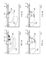
- Figures 3a to 3d show the evolution of the areas of impact ionization and the boundary of the depletion region at periods of 0.4 pico-seconds, 0.6 nano-seconds (ns), 15 ns and 100 ns respectively, after the application of an ESD event.
- the edge of the collector doping is represented by dashed line 300.
- the spatial extent of the depletion region is represented by chain dot line 302. Areas of relatively high impact ionization are denoted by the shaded regions 310 and areas of lesser, but still significant impact ionization are denoted by the areas 320.
- Impact ionization tends to be concentrated in areas of high field strength, or areas of moderate field strength and high current density.
- the diode breakdown of the collector-base diode has initiated, with areas 310 exhibiting very large impact ionization, and areas 320 exhibiting lesser amounts of impact ionization.
- the depletion region 302 is following the profile of a device in its non-conducting state.
- the device is starting to conduct collector current, and hence the extent of the area of impact ionization near the surface of the device is becoming reduced as the potential difference across the device in that region becomes reduced.
- the device is mainly turned on and areas of impact ionization are relatively modest and constrained to the regions 320.
- the inventors investigated options for modifying the devices shown in Figure 1 and 2 so as to further improve its turn on time whilst still allowing the breakdown and holding voltages to be layout adjustable and/or to be controlled by external components.
- FIG 4 schematically illustrates a protection device or circuit 400 incorporating a bipolar NPN transistor 405, which can be implemented using the bipolar transistor configurations shown in Figure 1 or 2 .
- a node 410 corresponds to a node to be protected from overvoltage, such ESD and/or EOS events.
- a circuit to be protected by the protection circuit 400 can be electrically connected to the node 410.
- the transistor 405 has its collector connected to the node 410 which is protected from overvoltage events by the protection circuit 400 comprising the transistor 405.
- the node 410 may be any node within an integrated circuit, such as an input node or output node, an internal node or one of the power rails.
- the protected node 410 is coupled to the base 420 of the transistor 405 by way of a capacitor 430.
- the capacitor 430 corresponds to an explicit capacitive structure rather than merely parasitic capacitance. In one embodiment, the capacitor 430 has a value greater that 40pF, for example, a value between 50pF and 100pF.
- a resistor 440 may be coupled between the base 420 and the emitter of the transistor 405, which may be connected to a local ground or a supply rail that serves as a discharge path 450 for the overvoltage event. Simulations of the device response were performed in respect of overvoltage events as defined by the IEC CDM standard in which the overvoltage event comprises a fast transient with a rise time of less than 1 ns.
- Figure 5 compares the clamping effect of the device when exposed to an IEC overvoltage event, when there is no capacitor 430 provided and when an 800 fF (8 x 10 -13 F) capacitor 430 is provided. It can be seen in the absence of the capacitor the transient voltage exceeded 150 volts, whereas in the presence the 800 fF capacitor the maximum voltage is just slightly over 100 volts. In both cases the device can be considered to be turned on by around 0.3 ns.
- Figure 6 is a graph comparing the transient response for the circuit 400 of Figure 4 when the capacitor 430 is disconnected and when the capacitor 430 has a value of 80 pF.
- Figure 6 shows the same data for the case in which the capacitor 430 is disconnected as Figure 5 , the graph is on a different scale.
- the maximum voltage transient was about 40 volts, with the device heading towards a holding voltage of 30 volts.
- the voltage overshoot is much reduced when using a 80 pF capacitor relative to a configuration in which the capacitor 430 is disconnected.
- Figure 7 shows similar data, but with the 80 pF capacitor either connected from the collector terminal to ground, or from the collector terminal to the base.
- the provision of the capacitor between the node to be protected (410) and ground limits the IEC overvoltage event to around 90 volts, whereas connecting the same capacitor between the node to be protected 410 and the base of the transistor 405 limits the overvoltage event in this example to around 50 volts.
- the simulations for Figures 6 and 7 were performed using slightly different device structures, in terms of feature sizes and doping levels, so the clamping voltages are slightly different, but this does not detract from the validity of these comparisons.
- FIG 8 substantially reproduces the transistor structure shown in Figure 2 , but also shows the bipolar current path 910 that the carriers take between the collector and the emitter of the bipolar device.
- Figure 9 shows a similar device, but where the base has now been modified such that it can now be regarded as being formed of first and second base regions 920 and 922.
- the first base region 920 is disposed adjacent the collector (or at least adjacent part of the collector or a collector-like implant that is electrically connected to the collector) such that a separation between the first base region 920 and the collector 200 (or a collector-like region electrically or physically connected to the collector) controls the trigger voltage by way of punch through and/or impact ionization trigger mechanisms.
- the second base region 922 forms a very thin base region extending beneath the emitter.
- the base of the bipolar device is tapered such that a thickness of the first base region 920 is greater than a thickness of the second base region 922.
- the base width of the second base region 922 is in the range of about 80nm to 100nm.
- the second base region 922 (disposed as a layer beneath the emitter region) can have a nominal width of substantially 80nm to 100nm for a 40 volt device.
- the provision of the thin second base region 922 allows the unity gain frequency fT to be increased from, for example, 22 MHz in the device of Figure 8 to 1.7 GHz in the device of Figure 9 where both transistors are fabricated using the same fabrication "process".
- the trigger voltage is layout adjustable by the distance between the edge of the base and the collector. This faster device can be achieved by doping the collector region such that it is spatially more extensive such that it underlies the base and emitter regions so as to promote a vertical current path 910. This may be achieved by varying (increasing) the doping in the epitaxial layer towards the surface of the transistor to make it more like the collector.
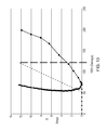
- Figure 10 compares the transient response of the transistor of Figure 8 with a transient response of the transistor of Figure 9 , designated 1000 and 1010, respectively. It can be seen that with the fast bipolar transistor there is effectively no overshoot whatsoever as the device is able to respond almost immediately.
- N c may be around 3 x 10 15 carriers per cubic cm.
- Jc may have a target value of no more than 50 ⁇ A per ⁇ m -2 .
- the target current may be around 60 amps, giving a device area of 320000 ⁇ m 2 .
- transistors shown in Figures 8 and 9 may be used in the current of Figure 4 , either with or without the provision of the capacitor 430.
- FIG 11 shows a further variation in which a protection transistor, for example of the type shown in Figure 1 , Figure 2 or Figure 9 , and designated 1100, is provided in a current flow path between a node to be protected 410 and a discharge path 450.
- the transistor 1100 may be provided in series with a second transistor 1102 similarly configured and a protection diode 1104 which serves to prevent reverse current flow.
- the protection diode 1104 can prevent a flow of current from the discharge path 450 to the node to be protected 410 when the voltage of the node to be protected 410 is less than that of the power low or ground supply associated with the discharge path 450.
- the transistors 1100 and 1102 exhibit slight leakage currents, then they will also share the voltage across them in a more or less equal manner. Thus, when a single transistor can protect to a magnitude of 40 volts, the 2 transistors can protect to 80 volts. This may be further extensible to higher voltages. Additionally a clamping diode or diodes 1120 are provided between the node to be protected 410 and the discharge path 450, together with a further protection diode 1125 which serves to prevent reverse current flow. The transistor 1100 and, where it is provided transistor 1102 may be provided with respective resistors 1130 and 1132 between their base and emitters in order to control the holding voltage of the device.
- Inductors may be used instead of or as well as resistors to control the flow of base current as this affects the holding voltage.
- the function of the diode 1120 is to breakdown rapidly and to clamp the voltage at the node to be protected 410 whilst the transistors 1100 and 1102 turn on.
- the transistors may be associated with further PNP transistors such that they form a silicon controlled rectifier arrangement.
- the transistors may further be associated with capacitors between their collectors and their base or between the node 410 and their bases in order to enhance device turn on time.
- the breakdown voltage for the transistor 1100 if only a single transistor is provided, or for the sum of the transistors where a plurality of transistors are provided in series, is set to be less than the breakdown voltage for the clamping diode. This ensures that the transistors turn on.
- a similar circuit can be built around PNP lateral transistors to provide protection against ESD events of opposite polarity.
- Figure 12 schematically illustrates and compares the operation of a diode clamp arranged to break down at 70 volts with that of the transistor 1100 optionally with transistor 1102 provided and operating to provide voltage clamping and fold-back.
- the bipolar transistor based protection device after breakdown or a trigger occurs, the voltage folds back to a holding voltage of around 50 to 55 volts, and then slowly increases as the ESD current increases giving an effective on resistance of about 1.7 ohms, as shown by line 1200.
- the diode exhibits a resistive characteristic once it starts to conduct, and therefore the voltage continues to rise with increasing ESD current as represented by line 1202.
- reducing the diode resistance can be achieved by placing a plurality of diodes in parallel, which is equivalent to making one larger (wider) diode. This can however be expensive in terms of die space or area.
- One approach to reducing the area overhead is to change the diode breakdown voltage such that is comes on (breaks down) at a lower voltage closer to the nominal holding voltage of the transistor.
- the effective on resistance of the diode can be calculated at 5.8 ohms.
- the diode area can be significantly smaller.
- having a lower breakdown voltage generally requires fewer series connected diodes in order to achieve that breakdown voltage giving a further reduction in die area.
- reducing the break-down voltage reduces the die area required.
- Figures 14 and 15 compare die area as a function of diode type in order to illustrate how choice of diode technology can also be significant. In each case, a breakdown voltage of around 40 volts is desired. For Figure 14 , Schottky diodes were used each having a breakdown voltage at 13.61 volts when reversed biased, and as such three series connected diodes are used in order to give the desired breakdown voltage.
- Zener diodes breakdown at approximately 5.15 volts when reversed biased and consequently eight are used in series. However, when the diodes become conducting they give an effective on resistance of 270 ohms. Thus, taking the number of series diodes that are used to achieve the breakdown voltage, and the number of parallel paths that are required to achieve the desired on resistance, this gives rise to an area multiplication of 1038 which, taking account of the Zener device size, gives a footprint of approximately 96,858 ⁇ m 2 on the die.
- Diode area can be reduced by employing vertically fabricated diodes.
- Figure 16 is a cross section through a vertical diode formed in accordance with an embodiment of the present invention.
- an N- type epitaxial layer 1600 is formed over a substrate 1602, and may be separated therefrom by an insulating layer associated with silicon on insulator (SOI) fabrication processes.
- SOI silicon on insulator
- an N region 1610 is formed over the N type region 1600, and brought to the surface where it makes contact with conductors 1620, operationally by way of highly doped N++ regions 1622.
- a P type region 1630 is formed within the N well 1610 and makes electrical connection to a further contact 1640, optionally by way of a highly doped P++ region 1642.
- the highly doped regions 1622 and 1642 are included to reduce the Ohmic resistance to the contacts.
- the P type region 1630 and N type region 1610 may undergo impact ionization driven breakdown.
- the physical structure of the diode arrangement shown in Figure 16 tends to cause the impact ionization to be fairly uniformly distributed along the lower surface of region 1630.
- the breakdown voltage of the diode is relatively easily controlled by manipulating the acceptor concentration of impurities in the P+ region 1630.
- the breakdown voltage is approximately 11.9 volts. If the impurity concentration is reduced to 6.4 x 10 12 , then the breakdown voltage is increased to approximately 46 volts. Reducing the impurity concentration to 4.4 x 10 12 gives rise to a breakdown voltage of approximately 51.9 volts, whereas reducing the impurity concentration to 2.0 x 10 12 atoms per cubic cm gives rise to breakdown voltage of approximately 62.3 volts.
- the doping concentration inversely controls the width of the depletion region, which in turn controls the breakdown voltage.
- the bipolar transistor structure can be varied in order to promote punch through between the collector and emitter.
- the collector and emitter regions may be formed adjacent one another as shown in Figure 17 .
- the collector 200 and its contact region 200a are formed as was before described with respect to Figure 2 .
- the emitter is, in this example, now comprised of very highly doped region 210a positioned beneath the emitter contact of electrode 212.
- the electrode 212 may be extended towards the collector, but does not touch it, so as to form a field plate (which may also be referred to as a resurf structure).
- the base can be formed of heavily doped region 220, which connects the base to the P+ material or region 223 of the body.
- the emitter and collector contact regions are adjacent one another (in that the base contact is not between them) but are not contiguous with one another.
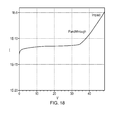
- punch through can, for example, start to become significant at voltages of around 35 volts or so, where it starts to increase the device current above the device leakage current of around 10 -12 amps. Punch through then remains dominant from about 35 volts to about 45 volts where impact ionization takes over to provide a greater base current to the device.
- Figure 19 compares the speed of the punch through device shown in Figure 17 with that of the device shown in Figure 2 .
- the time taken to turn the punch through device on is significantly less compared to the device of Figure 2 , and that manifests itself in a reduced voltage spike under the IEC test conditions.
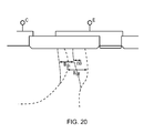
- the designer should take account of the kirk effect when operating a punch through transistor because, as shown in Figure 20 , the base width changes by a value ⁇ B between a device operating in the on condition as represented by chain-dot lines and having an effective base width B on , and the off condition as represented by chain lines and having an effective base width B off , where these lines represent the effective boundary regions of the base region.
- the holding voltage becomes related to the trigger voltage.
- Doping concentrations and device dimensions can determine the trigger voltage, but the emitter can generally be manipulated to change the holding voltage.
- the emitter depth can be made deeper or shallower to vary the holding voltage. Varying the emitter depth varies the base current and hence the gain of the transistor, and the holding voltage is substantially inversely proportional to the gain. Furthermore the distance between the base and the emitter can also be varied to adjust the gain of the device and hence its holding voltage.
- Figure 21 illustrates a further modification, which in many ways is similar to that shown in Figure 17 , except that now rather than extending the emitter electrode towards the collector, the collector electrode 202 is extended towards the emitter region.
- a separate electrode could be fabricated between the collector and emitter regions and biased to an appropriate voltage.
- the electrode may be formed of metal or polysilicon.
- an extension portion 202a of the collector electrode 202 is separated from the P type body 223 of the transistor by way of an insulating region 228.
- the electrode extension 202a effectively forms a gate region between the emitter region 210a and the collector region 200.
- MOSFET transistor which is coincident with the NPN bipolar transistor.
- the MOSFET action can be quite rapid giving rise to the formation of a relatively shallow conductive channel at the surface of the device.
- the conductive channel connects the collector and emitter regions together, such that they function as the drain and source of the MOSFET. Meanwhile the voltage may still start to build across the bipolar transistor even as the MOSFET turns on, giving rise to punch through and/or impact ionization driven breakdown mechanisms.
- the punch through transistor structure of Figure 17 can be formed in association with the high voltage MOS of Figure 21 in the same device due to the fact that the collector and emitter regions are formed adjacent one another, and that the base contact region is formed to one side of the device so as not to be between the collector and emitter.
- a thin base region 922 as described with respect to Figure 9 may be included beneath the emitter 210a in the devices as shown in Figures 17 and 21 .
- the profile of the collector electrode may, when viewed from above, have an irregular shape, thus the extension 202a may be formed in some areas of the collector electrode 202 but not in others such that some parts of the device are definitely more bipolar-like and some parts of the device are more field effect transistor-like. It is also possible to vary the doping concentration at the surface of the device, in those regions where it will cooperate with the collector extension 202a (or with a separately formed electrode) to modify the electrical properties of the field effect transistor.
- the device shown in Figure 21 may be substantially linear, or may exhibit reflection or rotational symmetry. Thus, for example, the device could exhibit reflection or rotational symmetry around the base/gate electrode 222, or indeed around the drain/collector electrode if this was desired. Under such circumstances the extension 202a would extend from either side of the region 200a.
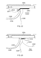
- Figure 22 is a simulation showing where the channel current predominantly flows during the conduction phase of the field effect transistor. As shown in Figure 22 , the channel current is constrained to a relatively thin region 2310 as it passes between the emitter and collector regions before fanning out into a broader region 2312.
- the chain line 2314 represents in broad terms the spatial extent of the channel
- the chain-dot lines 2320 represent the edges of the depletion region
- the solid line 2330 represents the nominal spatial extent of the drain doping.
- Figure 23 is similar to Figure 22 , but shows the regions of current flow of the base current once the bipolar action has become established.
- the base current occurs in region 2400 whose boundaries are delimited by the chain lines 2402.
- punch-through transistor or punch-through plus FET transistor structures described here can be used in the circuits described with respect to Figures 4 and 11 , and also with the vertical diode structures.
- the transistor of Figure 2 can be modified to increase the relative interface area between the base and collector regions thereof.
- An example of such a device is shown in Figure 24 where a further base contact 222' and a further base region 220' are formed towards the left hand side of the Figure complimenting the base regions 200 and 222 formed towards the right hand side of the Figure.
- Including the further base contact 222' and further base region 220' provides an increased reversed biased diode area between the collector and base regions such that once the diode starts to break down there is more volume of semiconductor involved in the conduction, and hence the on resistance of the diode is less.
- the breakdown of the intrinsic diode limits voltage drives across the device during the time period taken for the bipolar transistor to become conductive.
- Figure 25 schematically illustrates areas 2600 where impact ionization triggers the formation of a base current.
- the impact ionization area is roughly doubled, giving rise to more base current to turn the transistor on and reduced resistance while the collector base junction acts as a clamping diode while the transistor or silicon controlled rectifier is in the process of turning on.
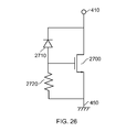
- the arrangement shown in Figure 11 may be modified such that a reversed biased diode is arranged to breakdown at a trigger voltage, and to turn a fast field effect transistor on.
- a FET 2700 is connected between the node to be protected 410 and the discharge path 450.
- the gate of the transistor could be directly connected to the source of the transistor if the threshold voltage V TH of the device is set to a suitable value to act as a trigger voltage, either by doping or by spacing of the gate above the semiconductor forming the FET.
- a reverse biased diode 2710 having a suitable trigger voltage can be connected between the node to be protected 410 and a gate of the FET 2700.
- a resistor 2720 can be provided to hold to gate voltage at the voltage of the discharge path, thereby presenting leakage currents in the diode 2710 turning the transistor on.
- the transistor of claim 26 may further be provided in combination with a capacitor to inject into the base, the diodes may be selected in accordance with the teachings given herein, and may Schottky diodes, Zener diodes or other suitable diode technology, be that formed horizontally or vertically.
Landscapes
- Engineering & Computer Science (AREA)
- Power Engineering (AREA)
- Semiconductor Integrated Circuits (AREA)
- Bipolar Integrated Circuits (AREA)
- Metal-Oxide And Bipolar Metal-Oxide Semiconductor Integrated Circuits (AREA)
Abstract
Description
- This disclosure relates to circuits to provide other components with protection against overvoltage, such as electrostatic discharge (ESD) and/or electrical overstress (EOS) events.
- Modern electronics relies on integrated circuits where large numbers of transistors are provided within a single package. For performance, such as speed, the transistors are often designed to operate at relatively low voltages, for example, between a few volts and a few tens of volts.
- Integrated circuits are packaged to protect them, but need to connect to components outside of the package by way of legs or pins or similar structures. These may in turn connect to terminals, connectors or sockets provided on a product in which the integrated circuit is provided. Thus, even when an integrated circuit is mounted on a circuit board, it can be subjected to electrostatic shocks. It is known that integrated circuits waiting to be placed on a circuit board are especially vulnerable to electrostatic discharge or other overvoltage events.
- It is desirable, and known, to provide circuits that provide overvoltage protection. Simple examples are the provision of reverse biased diodes between a node to be protected and the supply rails of an integrated circuit.
- However, in more sophisticated voltage protection circuits it is desirable that:
- 1) The circuit does not trigger until a trigger voltage is reached.
- 2) That once the circuit has triggered, the voltage "snaps back" to a smaller holding voltage.
- 3) The circuit is fast so that it can respond to an ESD event before damage occurs to the integrated circuit.
- Performance of the circuits can be assessed against several published test standards. One such standard is the International Electrotechnical Commission (IEC) CDM (charged device model) where peak current can be in the range of 6A with a rise time of less than 400 pico-seconds. ESD events of this nature may give rise to gate oxide damage of MOSFETs, junction damage and charge trapping with integrated circuits.
- It is desirable to provide a robust and a fast protection circuit.
- According to a first aspect of this disclosure there is provided an overvoltage protection device comprising a bipolar transistor. The bipolar transistor has base, collector and emitter regions. The collector and emitter regions are provided adjacent one another.
- By varying the distance between the collector and emitter regions the voltage at which punch-through driven triggering of the overvoltage protection device occurs can be controlled. Thus, a particular distance between the collector and emitter regions can be selected to achieve a desired trigger voltage of the overvoltage protection device.
- A conductor may extend above a semiconductor between the collector and emitter regions and be electrically isolated from the semiconductor. The conductor can be held at a voltage, such as the emitter voltage, such that it acts as a field plate or resurf structure. Alternatively, the conductor may be used as a gate so as to form a MOSFET having a channel within the bipolar transistor.
- The overvoltage protection device may further comprise a capacitor connected between a node to be protected and the base (or base/gate) of the transistor.
- According to a second aspect of this disclosure there is provided an overvoltage protection device comprising a bipolar transistor structure. The bipolar transistor structure has base, collector and emitter regions. The collector and emitter regions are in a current flow path that is connected to a node to be protected from an overvoltage event. The current flow path extends to a discharge path. The overvoltage protection device further comprises a component, such as a suitably connected capacitor or diode, to facilitate turn on of the protection device.
- Advantageously a capacitor has a first terminal connected to the base terminal, and a second terminal connected to the collector and/or the node to be protected. In certain configurations the bipolar transistor structure may have a doping concentration within its various regions that makes the device asymmetric (i.e. the collector- base and base-emitter regions are different). However, it remains possible to provide a circuit where the bipolar transistor structure is symmetric or substantially symmetric, to give bi-directional protection. For example, a bi-directional protection device can be used to protect an integrated circuit from both a positive polarity ESD event and a negative polarity ESD event. In such an arrangement capacitors may connect between the base and the collector and between the base and the emitter.
- The bipolar transistor structure may be associated with a second bipolar transistor structure to form a silicon controlled rectifier (SCR). Regions of silicon may be shared by both of the transistors.
- The base of the bipolar transistor structure may be connected to a second current flow path having at least one of a resistive impedance and an inductive impedance to control base current in the transistor when the transistor is on.
- According to a third aspect of this disclosure there is provided an overvoltage protection device comprising a bipolar transistor, wherein the bipolar transistor has base, collector and emitter regions. The collector is connected to a node to be protected and the emitter is connected to a discharge path, such as a power rail or ground supply. The transistor has a relatively thin base region disposed beneath (or above) the emitter region. It is thus possible to modify the structure of the bipolar transistor to make it respond more quickly. For example, implementing the bipolar transistor with a relatively thin base region can improve turn-on speed, which can aid in reducing voltage build-up during an ESD and/or EOS event.
- In an embodiment the overvoltage protection device comprises a bipolar transistor connected between a node to be protected and a discharge path. The base width of the transistor is selected such that carrier transit time across the base gives rise to a unity gain frequency (FT) value of the transistor substantially equal to an inverse of a rise time of an ESD event. Preferably, the FT value is greater than 1GHz such that the corresponding rise time is less than one nanosecond.
- Preferably, the transistor base further comprises a further base region disposed adjacent the collector, but separated therefrom. The further base region and the collector are separated by a region of reduced doping. The distance by which the collector and the further base region are separated controls a breakdown voltage of the device.
- According to a fourth aspect of this disclosure there is provided an overvoltage protection device comprising a transistor or a silicon controlled rectifier in combination with at least one clamping diode.
- The clamping diodes may be provided in parallel and series to synthesize a composite diode having desirable electrical characteristics. The diode or composite diode may be provided in parallel with the transistor or the silicon controlled rectifier. Additionally or alternatively the clamping diodes may be connected to a control node of the transistor or silicon controlled rectifier. The transistor may be a bipolar transistor or a FET.
- In another aspect, a method of providing overvoltage protection to a node is provided. The method includes forming a transistor having a body of a first type of semiconductor and first and second regions of a second type of semiconductor, one of the first and second regions being connected to a node to be protected and the other of the regions being connected to a discharge path. Additionally, one or more of the following apply: (a) the body forms a base region of the transistor and a capacitance is provided between the node to be protected and the body region to inject change to turn the transistor on; (b) a layer of the first type of semiconductor is provided beneath the one of the regions that acts as an emitter of the transistor to form a bipolar transistor with a unity gain frequency of greater than 1GHz; (c) at least one clamping diode extends between the first and second regions; (d) the first and second regions are adjacent one another but not contiguous such that punch through occurs to indicate conduction in the transistor; (e) the first and second regions are adjacent one another and separated from one another, and a gate electrode is formed between them to allow a voltage at the node to be protected in excess of a threshold voltage to cause conduction between the first and second regions along a channel; (f) the base-collector interface region is enlarged by forming the base on either side of or at least partially around the region connected to the node to be protected; and/or (g) the transistor forms a field effect transistor and a clamping diode is connected to the gate of the field effect transistor to turn it one once a breakdown voltage for the diode is reached.
- Embodiments of overvoltage protection devices will now be described, by way of non-limiting example, with reference to the accompanying drawings.
-
Figure 1 shows a known ESD protection device as described inUS2011-0101444 . -
Figure 2 is a cross-section through a lateral NPN transistor which serves as representative device for the purposes of modelling or testing how changes can modify the turn on time of a protection device. -
Figure 3a to 3d show the evolution of regions in impact ionization in response to an overvoltage (ESD) event. -
Figure 4 is a circuit diagram where the lateral NPN transistor ofFigure 2 has its collector connected to a node that is to be protected from ESD events, and where a capacitor is connected between the node to be protected and the base of the transistor. -
Figure 5 is a graph comparing transient response for the circuit ofFigure 4 where the capacitor is disconnected, and when it has a value of 800 fF. -
Figure 6 is a graph comparing the transient response for the circuit ofFigure 4 when the capacitor is disconnected and when it has a value of 80 pF. -
Figure 7 is a graph comparing the response when and 80 pF capacitor is connected between the node to be protected and ground, with the response of connecting the capacitor to the base of the transistor. -
Figure 8 reproduces the transistor as shown inFigure 2 , with the addition of an indication of the base width and the bipolar path within the transistor. -
Figure 9 shows a modified structure where the base is much thinner. -
Figure 10 compares the response of the collector voltage as a function of time for the transistor ofFigure 9 compared to that ofFigure 2 . -
Figure 11 shows a modified protection device with parallel protection diodes. -
Figure 12 is a graph showing node voltage versus current flow at a node protected by the circuit shown inFigure 11 . -
Figure 13 is a graph illustrating how choosing a reduced clamping voltage for the clamping diode facilitates limiting the peak voltage for a maximum node current. -
Figure 14 is a graph illustrating Schottky diode performance for the purpose of calculating die area required for the clamping diode ofFigure 11 . -
Figure 15 is a graph illustrating Zener diode performance for the purpose of calculating the die area required. -
Figure 16 is a cross-section through a modified diode structure so as to form a vertical diode. -
Figure 17 is a cross-section through a modified transistor structure where the collector and emitter regions are formed adjacent each other to facilitate punch through of the transistor. -
Figure 18 is a graph showing a simulation of the I-V characteristic of the device shown inFigure 17 in a nominally off state, and indicating where punch through and then impact ionization effects start to turn the transistor on. -
Figure 19 compares the transient response of the punch through transistor ofFigure 17 with that of the transistor ofFigure 2 in response to an IEC CDM event. -
Figure 20 schematically illustrates effective base width modulation in the punch through transistor ofFigure 17 . -
Figure 21 is a cross section through a further embodiment of a protection device where a bipolar transistor and a field effect transistor are substantially coincident within the semiconductor material. -
Figure 22 shows regions of channel current within the transistor shown inFigure 21 . -
Figure 23 shows regions of base current within the transistor shown inFigure 21 . -
Figure 24 shows a further modification to the arrangement shown inFigure 2 . -
Figure 25 shows regions of impact ionization in the device ofFigure 24 . -
Figure 26 shows a further embodiment of a protection device. -
US 2011-0101444 discloses anovervoltage protection device 5 based around a horizontal NPN transistor which is formed within an insulated well, although it should be understood that this disclosure is not limited to the use of such silicon-on-insulator transistors. Such a device is shown inFigure 1 . - As shown in
Figure 1 , a layer ofinsulation 22 is formed over asubstrate 10. The substrate may be a semiconductor. Advantageously the semiconductor is silicon, but other semiconductors may also be used. A relatively heavily dopedP+ layer 24 is provided over the layer ofinsulation 22 or just over part of it which in the finished device is beneath a base region B of the transistor as shown inFigure 1 . Anepitaxial layer 30 of P type material is provided over theP+ region 24. The P type material of theepitaxial layer 30 forms a body of the overvoltage protection device. TheP+ region 24 helps inhibit the formation of parasitic vertical transistors and also, being heavily doped, helps to shield the base region B and emitter region E of the device from electrostatic fields resulting from theepitaxial layer 30 being at a different potential relative to thesubstrate 10. - A first
N type region 40 is formed, as shown inFigure 1 , towards the left hand side of the device. Thedevice 5 in this example has rotational symmetry such that thesame region 40 also exists on the right hand side of thedevice 5. This region forms a collector C. - A
P+ region 50 is implanted to form a base region B, theP+ region 50 being implanted adjacent but spaced apart from theN type region 40. Afurther N+ region 60 that forms the emitter E is implanted within theP+ region 50. As thetransistor 5 is deliberately fabricated as a horizontal structure, thecollector regions 40 need only be provided in the vicinity of the surface. Alternatively the N+ region 40 can be extended by formingregion 40a, orregions region 40b may be implanted, or otherwise doped, before thelayer containing region 40a is grown on the wafer. Similarly,region 40a may be implanted with dopant before a toplayer containing region 40 is grown on the wafer or it can be done at the same time. - For a bidirectional overvoltage protection device that provides protection against an overvoltage condition, such as an electrostatic discharge event, of either polarity it is preferable for the
regions - In the example discussed here, the
N type regions epitaxial layer 30 associated with the P type body is more lightly doped at around 1015 acceptor impurities per cubic centimeter. - Such a device triggers automatically as the voltage across it increases. The trigger mechanism is provided and controlled by controlling the lateral extent of a distance D between the edge of the collector region and the edge of the base region to adjust the trigger voltage, and distance L representing the width of the base region to adjust the holding voltage.
- The distances D and L can be selected at production by the use of mask positioning. Thus, by controlling the distances D and L the voltage at which punch through occurs and triggers the device to conduct can be controlled. Device triggering can also be controlled through adjusting impact ionization driven breakdown mechanisms.
- The holding voltage of the device can also be controlled by controlling the base current in the horizontal transistor.
- The above device meets the transmission-line pulse (TLP) test requirements in terms of transient response. However, the response of the horizontal NPN transistor that provides the overvoltage and ESD protection is constrained by device physics.
- In somewhat simplistic terms, the current flow in a semiconductor device could be attributed to the combination of minority carrier current flow and to majority carrier current flow. Typically, majority carrier current flow mechanisms are relatively fast, whereas minority carrier mechanisms are relatively slow.
- If we consider the turn on mechanism of the device of
Figure 1 due to impact ionization, then as the voltage across the device rises the collector-base voltage gives rise to impact ionization which has a very rapid (for example, sub pico-second) response time as it is a majority carrier breakdown event. However, the impact-ionization initiated breakdown is used to inject electrons into the P type material of the bipolar transistor, and as this is a minority carrier current flow it is somewhat slower, thereby giving rise to a restriction in the natural turn on time of such a device. - Although the overvoltage protection based around the transistor shown in
Figure 1 may further include a vertical transistor within them for providing an SCR action, for the purposes of simulating and explaining modifications to the turn on time, only the action of the lateral transistor need be considered. - Transistor operation was simulated by the inventors for a lateral NPN transistor whose structure is shown in
Figure 2 . The transistor shown inFigure 2 comprises acollector region 200 formed beneath acollector contact 202, anemitter region 210 beneath anemitter contact 212, and abase region 220 beneath abase contact 222. All these regions are provided within anepitaxial layer 223. Theregions region 220 is highly doped P type silicon. Additional very highlydoped regions emitter contacts oxide layer 225 and a further insulatinglayer 228 which may also be oxide or might be a nitride or other suitable dielectric material. It will be appreciated that by swapping the semiconductor device a PNP transistor can be formed. For example, the doping types of all the layers, regions, and wells of the protection device can be opposite to those described above to provide a PNP transistor. - Optionally a second base contact B', formed by a diffusion 220' and associated via can be made on the other side of the
collector 200, as shown. The second base contact B' makes the device more symmetric (from an electrical point of view) and helps prevent lateral punch through where a depletion region from the collector travels around the device (for a device not having a ring shaped collector encircling the base and emitter when viewed from above) to the emitter. -
Figures 3a to 3d show the evolution of the areas of impact ionization and the boundary of the depletion region at periods of 0.4 pico-seconds, 0.6 nano-seconds (ns), 15 ns and 100 ns respectively, after the application of an ESD event. In each of the Figures the edge of the collector doping is represented by dashedline 300. Similarly the spatial extent of the depletion region is represented bychain dot line 302. Areas of relatively high impact ionization are denoted by the shadedregions 310 and areas of lesser, but still significant impact ionization are denoted by theareas 320. - Impact ionization tends to be concentrated in areas of high field strength, or areas of moderate field strength and high current density. Starting through the time sequence (
Figure 3a ), at 0.4 ps the diode breakdown of the collector-base diode has initiated, withareas 310 exhibiting very large impact ionization, andareas 320 exhibiting lesser amounts of impact ionization. It can also be seen that, for most of the device thedepletion region 302 is following the profile of a device in its non-conducting state. After 0.6 ns (Figure 3b ) the device is starting to conduct collector current, and hence the extent of the area of impact ionization near the surface of the device is becoming reduced as the potential difference across the device in that region becomes reduced. - By the
time 15 ns is reached, as shown inFigure 3c , the device is mainly turned on and areas of impact ionization are relatively modest and constrained to theregions 320. - By 100 ns the device is fully turned on and very little has changed comparing
Figure 3d to Figure 3c . - Had the electron current been illustrated, then at 0.4 ps and 0.6 ns there would have been a relatively strong electron flow between the base and collector contacts. However, by 15 ns and 100 ns, this flow would be significantly reduced as the normal transistor action takes over.
- The inventors investigated options for modifying the devices shown in
Figure 1 and2 so as to further improve its turn on time whilst still allowing the breakdown and holding voltages to be layout adjustable and/or to be controlled by external components. - Several ways were identified, and one or more of the following options can be used either alone or in combination:
- 1. Connect a capacitor between the collector and the base so as to turn the bipolar transistor on more quickly. The capacitance reduces the switch on time because it is no longer necessary to wait for impact ionization to provide the entirety of the base current to the bipolar transistor.
- 2. Provide a high speed bipolar transistor, having the same architecture, but with a smaller base width (i.e. vertical depth). A reduction in base width reduces the time for the minority carriers to propagate across the emitter-base junction, and thereby speeds up the response of the device. However fast transistors tend to take up significantly more area, generally between five and ten times the area so the cost involved is significantly greater.
- 3. Provide a clamping diode across the transistor. Such a diode can be provided as a parallel device, but takes up area on the chip. In such an arrangement it may be desirable to reduce the trigger voltage of the transistor such that it is closer to the holding voltage, which gives a bigger voltage window in which to operate the diode. As diodes can be quite resistive the diode needs to be physically expansive. Schottky and Zener diodes may be used as they give localized breakdown. In order to reduce the amount of "real estate" or area required on the semiconductor substrate a vertical diode may be provided. A vertical diode gives a more uniform breakdown characteristic, and the breakdown occurs over a bigger area. Thus the device is more area efficient relative to a lateral diode. In some embodiments the diode can be provided internally to the transistor by making the transistor symmetric, and putting the base on the outer side of the collector.
- 4. Provide a punch through diode by adjusting the space between the collector and the emitter.
- 5. Provide a high voltage MOS device. This can be achieved by forming a plate over the silicon between the collector and the base, thereby effectively forming a channel at the surface of the device which provides a fast MOSFET within the structure of a bipolar transistor. As the MOS channel conducts, this gives rise to impact ionization at the drain/collector edge which gives rise to a current which provides a base current to turn the bipolar transistor on.
- 6. Provide an intrinsic diode.
- 7. Replace the bipolar transistor which a fast MOS device and clamping.
-
Figure 4 schematically illustrates a protection device orcircuit 400 incorporating abipolar NPN transistor 405, which can be implemented using the bipolar transistor configurations shown inFigure 1 or2 . Anode 410 corresponds to a node to be protected from overvoltage, such ESD and/or EOS events. A circuit to be protected by theprotection circuit 400 can be electrically connected to thenode 410. - The
transistor 405 has its collector connected to thenode 410 which is protected from overvoltage events by theprotection circuit 400 comprising thetransistor 405. Thenode 410 may be any node within an integrated circuit, such as an input node or output node, an internal node or one of the power rails. The protectednode 410 is coupled to thebase 420 of thetransistor 405 by way of acapacitor 430. Thecapacitor 430 corresponds to an explicit capacitive structure rather than merely parasitic capacitance. In one embodiment, thecapacitor 430 has a value greater that 40pF, for example, a value between 50pF and 100pF. Optionally aresistor 440 may be coupled between the base 420 and the emitter of thetransistor 405, which may be connected to a local ground or a supply rail that serves as adischarge path 450 for the overvoltage event. Simulations of the device response were performed in respect of overvoltage events as defined by the IEC CDM standard in which the overvoltage event comprises a fast transient with a rise time of less than 1 ns. -
Figure 5 compares the clamping effect of the device when exposed to an IEC overvoltage event, when there is nocapacitor 430 provided and when an 800 fF (8 x 10-13F)capacitor 430 is provided. It can be seen in the absence of the capacitor the transient voltage exceeded 150 volts, whereas in the presence the 800 fF capacitor the maximum voltage is just slightly over 100 volts. In both cases the device can be considered to be turned on by around 0.3 ns. -
Figure 6 is a graph comparing the transient response for thecircuit 400 ofFigure 4 when thecapacitor 430 is disconnected and when thecapacitor 430 has a value of 80 pF. AlthoughFigure 6 shows the same data for the case in which thecapacitor 430 is disconnected asFigure 5 , the graph is on a different scale. Here it can be seen that with an 80pF capacitor the maximum voltage transient was about 40 volts, with the device heading towards a holding voltage of 30 volts. Thus the voltage overshoot is much reduced when using a 80 pF capacitor relative to a configuration in which thecapacitor 430 is disconnected. -
Figure 7 shows similar data, but with the 80 pF capacitor either connected from the collector terminal to ground, or from the collector terminal to the base. The provision of the capacitor between the node to be protected (410) and ground limits the IEC overvoltage event to around 90 volts, whereas connecting the same capacitor between the node to be protected 410 and the base of thetransistor 405 limits the overvoltage event in this example to around 50 volts. The simulations forFigures 6 and7 were performed using slightly different device structures, in terms of feature sizes and doping levels, so the clamping voltages are slightly different, but this does not detract from the validity of these comparisons. - A further approach which can be used to enhance turn on time is to modify the transistor structure in order to make it faster.
Figure 8 substantially reproduces the transistor structure shown inFigure 2 , but also shows the bipolarcurrent path 910 that the carriers take between the collector and the emitter of the bipolar device. By way of contrast,Figure 9 shows a similar device, but where the base has now been modified such that it can now be regarded as being formed of first andsecond base regions first base region 920 is disposed adjacent the collector (or at least adjacent part of the collector or a collector-like implant that is electrically connected to the collector) such that a separation between thefirst base region 920 and the collector 200 (or a collector-like region electrically or physically connected to the collector) controls the trigger voltage by way of punch through and/or impact ionization trigger mechanisms. Thesecond base region 922 forms a very thin base region extending beneath the emitter. In the illustrated configuration, the base of the bipolar device is tapered such that a thickness of thefirst base region 920 is greater than a thickness of thesecond base region 922. In one embodiment, the base width of thesecond base region 922 is in the range of about 80nm to 100nm. For example, the second base region 922 (disposed as a layer beneath the emitter region) can have a nominal width of substantially 80nm to 100nm for a 40 volt device. - The provision of the thin
second base region 922 allows the unity gain frequency fT to be increased from, for example, 22 MHz in the device ofFigure 8 to 1.7 GHz in the device ofFigure 9 where both transistors are fabricated using the same fabrication "process". Furthermore in each case the trigger voltage is layout adjustable by the distance between the edge of the base and the collector. This faster device can be achieved by doping the collector region such that it is spatially more extensive such that it underlies the base and emitter regions so as to promote a verticalcurrent path 910. This may be achieved by varying (increasing) the doping in the epitaxial layer towards the surface of the transistor to make it more like the collector. - As persons of ordinary skill in the art will appreciate, there is an optimum speed for a fast bipolar transistor which is a function of current, as initially increasing the device current causes the peak speed to be increased, but as the current rises further the Kirk effect takes over and starts to reduce the device speed. As persons of ordinary skill in the art will appreciate, the Kirk effect causes the base width to increase at higher current densities.
-
Figure 10 compares the transient response of the transistor ofFigure 8 with a transient response of the transistor ofFigure 9 , designated 1000 and 1010, respectively. It can be seen that with the fast bipolar transistor there is effectively no overshoot whatsoever as the device is able to respond almost immediately. - For the fast bipolar transistor the current density

where - Jc is the current density,
- q is the charge on the electron,
- vs is the electron thermal velocity,
- Nc is the number of carriers.
- For a device Nc may be around 3 x 10¹⁵ carriers per cubic cm. Jc may have a target value of no more than 50 µA per µm-2. The target current may be around 60 amps, giving a device area of 320000 µm2.
- It is possible to trade off device size by making the transistor less fast, having a slightly wider base or design that is nearer to that of
Figure 8 , and introducing a capacitance between the base and collector in order to enhance turn on time. Thus the transistors shown inFigures 8 and 9 may be used in the current ofFigure 4 , either with or without the provision of thecapacitor 430. -
Figure 11 shows a further variation in which a protection transistor, for example of the type shown inFigure 1 ,Figure 2 orFigure 9 , and designated 1100, is provided in a current flow path between a node to be protected 410 and adischarge path 450. Thetransistor 1100 may be provided in series with asecond transistor 1102 similarly configured and aprotection diode 1104 which serves to prevent reverse current flow. For example, theprotection diode 1104 can prevent a flow of current from thedischarge path 450 to the node to be protected 410 when the voltage of the node to be protected 410 is less than that of the power low or ground supply associated with thedischarge path 450. If thetransistors diodes 1120 are provided between the node to be protected 410 and thedischarge path 450, together with afurther protection diode 1125 which serves to prevent reverse current flow. Thetransistor 1100 and, where it is providedtransistor 1102 may be provided withrespective resistors diode 1120 is to breakdown rapidly and to clamp the voltage at the node to be protected 410 whilst thetransistors Figure 4 , the transistors may further be associated with capacitors between their collectors and their base or between thenode 410 and their bases in order to enhance device turn on time. The breakdown voltage for thetransistor 1100 if only a single transistor is provided, or for the sum of the transistors where a plurality of transistors are provided in series, is set to be less than the breakdown voltage for the clamping diode. This ensures that the transistors turn on. A similar circuit can be built around PNP lateral transistors to provide protection against ESD events of opposite polarity. -
Figure 12 schematically illustrates and compares the operation of a diode clamp arranged to break down at 70 volts with that of thetransistor 1100 optionally withtransistor 1102 provided and operating to provide voltage clamping and fold-back. For the bipolar transistor based protection device, after breakdown or a trigger occurs, the voltage folds back to a holding voltage of around 50 to 55 volts, and then slowly increases as the ESD current increases giving an effective on resistance of about 1.7 ohms, as shown byline 1200. By comparison the diode exhibits a resistive characteristic once it starts to conduct, and therefore the voltage continues to rise with increasing ESD current as represented byline 1202. This means that the voltage across the devices connected to thenode 410, which is supposed to be protected, may exceed a limit voltage, for example 120 volts where damage occurs. It is therefore desirable to reduce the apparent resistance of thediode 1120, which in this example is around 12 Ohms. - As known to the person skilled in the art, reducing the diode resistance can be achieved by placing a plurality of diodes in parallel, which is equivalent to making one larger (wider) diode. This can however be expensive in terms of die space or area. One approach to reducing the area overhead is to change the diode breakdown voltage such that is comes on (breaks down) at a lower voltage closer to the nominal holding voltage of the transistor. Thus, as shown in
Figure 13 , if the diode is arranged to turn on at about 50 volts, then in order to conduct a required maximum current of 12 amps without exceeding the 120 volt damage threshold, the effective on resistance of the diode can be calculated at 5.8 ohms. Hence the diode area can be significantly smaller. Furthermore, having a lower breakdown voltage generally requires fewer series connected diodes in order to achieve that breakdown voltage giving a further reduction in die area. Thus reducing the break-down voltage reduces the die area required. -
Figures 14 and 15 compare die area as a function of diode type in order to illustrate how choice of diode technology can also be significant. In each case, a breakdown voltage of around 40 volts is desired. ForFigure 14 , Schottky diodes were used each having a breakdown voltage at 13.61 volts when reversed biased, and as such three series connected diodes are used in order to give the desired breakdown voltage. - When the diodes turn on they have an effective resistance of 630 ohms. Placing banks of diodes in parallel allows the effective diode resistance to be reduced to a 2.6 ohm or 2.5 ohm target (use of the lower resistance allows the break-down voltage to be increased again), and taking this into consideration, we have an effective area multiplication of 969 times the unit diode size, giving a total die area of approximately 48,450 µm2.
- If the same performance is desired using Zener diode technology, then the Zener diodes breakdown at approximately 5.15 volts when reversed biased and consequently eight are used in series. However, when the diodes become conducting they give an effective on resistance of 270 ohms. Thus, taking the number of series diodes that are used to achieve the breakdown voltage, and the number of parallel paths that are required to achieve the desired on resistance, this gives rise to an area multiplication of 1038 which, taking account of the Zener device size, gives a footprint of approximately 96,858 µm2 on the die.
- Thus, it can be seen that despite the higher on resistance of the Schottky diodes, taking their breakdown voltage into account, the "real estate" or area on the die used to achieve the desired clamping performance is reduced compared to Zener diode technology.
- Diode area can be reduced by employing vertically fabricated diodes.
-
Figure 16 is a cross section through a vertical diode formed in accordance with an embodiment of the present invention. Thus, many steps of the fabrication process can be similar to that of the transistor shown inFigure 2 . In this example an N-type epitaxial layer 1600 is formed over asubstrate 1602, and may be separated therefrom by an insulating layer associated with silicon on insulator (SOI) fabrication processes. Next anN region 1610 is formed over theN type region 1600, and brought to the surface where it makes contact withconductors 1620, operationally by way of highly dopedN++ regions 1622. -
A P type region 1630 is formed within the N well 1610 and makes electrical connection to afurther contact 1640, optionally by way of a highly dopedP++ region 1642. The highlydoped regions P type region 1630 andN type region 1610 may undergo impact ionization driven breakdown. However, the physical structure of the diode arrangement shown inFigure 16 tends to cause the impact ionization to be fairly uniformly distributed along the lower surface ofregion 1630. Thus, because a significant proportion of the diode is used to conduct electricity under breakdown conditions, it provides a relatively compact structure. Furthermore, the breakdown voltage of the diode is relatively easily controlled by manipulating the acceptor concentration of impurities in theP+ region 1630. - For example, if the
region 1630 is doped at a concentration of approximately 1014 impurity atoms per cubic centimeter (which is similar to the doping of the region 1642) then the breakdown voltage is approximately 11.9 volts. If the impurity concentration is reduced to 6.4 x 10¹², then the breakdown voltage is increased to approximately 46 volts. Reducing the impurity concentration to 4.4 x 10¹² gives rise to a breakdown voltage of approximately 51.9 volts, whereas reducing the impurity concentration to 2.0 x 10¹² atoms per cubic cm gives rise to breakdown voltage of approximately 62.3 volts. The doping concentration inversely controls the width of the depletion region, which in turn controls the breakdown voltage. - In a further variation the bipolar transistor structure can be varied in order to promote punch through between the collector and emitter. In order to achieve this, the collector and emitter regions may be formed adjacent one another as shown in
Figure 17 . Here, thecollector 200 and itscontact region 200a are formed as was before described with respect toFigure 2 . However, the emitter is, in this example, now comprised of very highlydoped region 210a positioned beneath the emitter contact ofelectrode 212. Theelectrode 212 may be extended towards the collector, but does not touch it, so as to form a field plate (which may also be referred to as a resurf structure). The base can be formed of heavily dopedregion 220, which connects the base to the P+ material orregion 223 of the body. Thus the emitter and collector contact regions are adjacent one another (in that the base contact is not between them) but are not contiguous with one another. - In use, current flow between the collector and emitter is generally constrained to be near the surface of the device. This can provide a fast device because the base width in the conduction path is effectively very small due to the modified geometry of the device. The spacing between the collector and emitter regions can be adjusted to adjust the amount of punch through and the device turn on voltage. In simulations, and as shown in
Figure 18 , punch through can, for example, start to become significant at voltages of around 35 volts or so, where it starts to increase the device current above the device leakage current of around 10-12 amps. Punch through then remains dominant from about 35 volts to about 45 volts where impact ionization takes over to provide a greater base current to the device. -
Figure 19 compares the speed of the punch through device shown inFigure 17 with that of the device shown inFigure 2 . The time taken to turn the punch through device on is significantly less compared to the device ofFigure 2 , and that manifests itself in a reduced voltage spike under the IEC test conditions. However the designer should take account of the kirk effect when operating a punch through transistor because, as shown inFigure 20 , the base width changes by a value ΔB between a device operating in the on condition as represented by chain-dot lines and having an effective base width Bon, and the off condition as represented by chain lines and having an effective base width Boff, where these lines represent the effective boundary regions of the base region. - In the punch through device of
Figure 17 the holding voltage becomes related to the trigger voltage. Doping concentrations and device dimensions can determine the trigger voltage, but the emitter can generally be manipulated to change the holding voltage. For example the emitter depth can be made deeper or shallower to vary the holding voltage. Varying the emitter depth varies the base current and hence the gain of the transistor, and the holding voltage is substantially inversely proportional to the gain. Furthermore the distance between the base and the emitter can also be varied to adjust the gain of the device and hence its holding voltage. -
Figure 21 illustrates a further modification, which in many ways is similar to that shown inFigure 17 , except that now rather than extending the emitter electrode towards the collector, thecollector electrode 202 is extended towards the emitter region. Alternatively, a separate electrode could be fabricated between the collector and emitter regions and biased to an appropriate voltage. The electrode may be formed of metal or polysilicon. In the configuration illustrated inFigure 21 , anextension portion 202a of thecollector electrode 202 is separated from theP type body 223 of the transistor by way of aninsulating region 228. Thus, theelectrode extension 202a effectively forms a gate region between theemitter region 210a and thecollector region 200. Thus it is possible to fabricate a MOSFET transistor which is coincident with the NPN bipolar transistor. The MOSFET action can be quite rapid giving rise to the formation of a relatively shallow conductive channel at the surface of the device. The conductive channel connects the collector and emitter regions together, such that they function as the drain and source of the MOSFET. Meanwhile the voltage may still start to build across the bipolar transistor even as the MOSFET turns on, giving rise to punch through and/or impact ionization driven breakdown mechanisms. Thus the punch through transistor structure ofFigure 17 can be formed in association with the high voltage MOS ofFigure 21 in the same device due to the fact that the collector and emitter regions are formed adjacent one another, and that the base contact region is formed to one side of the device so as not to be between the collector and emitter. - It is believed that formation of the field effect transistor may, in fact, enhance operation of the bipolar transistor since formation of the relatively thin channel gives rise to impact ionization within the channel which in turn drives the base current of the bipolar transistor. Thus, the field effect transistor can to some extent be regarded as turning the bipolar transistor on. Additionally, a
thin base region 922 as described with respect toFigure 9 may be included beneath theemitter 210a in the devices as shown inFigures 17 and21 . - In some embodiments, the profile of the collector electrode may, when viewed from above, have an irregular shape, thus the
extension 202a may be formed in some areas of thecollector electrode 202 but not in others such that some parts of the device are definitely more bipolar-like and some parts of the device are more field effect transistor-like. It is also possible to vary the doping concentration at the surface of the device, in those regions where it will cooperate with thecollector extension 202a (or with a separately formed electrode) to modify the electrical properties of the field effect transistor. The device shown inFigure 21 may be substantially linear, or may exhibit reflection or rotational symmetry. Thus, for example, the device could exhibit reflection or rotational symmetry around the base/gate electrode 222, or indeed around the drain/collector electrode if this was desired. Under such circumstances theextension 202a would extend from either side of theregion 200a. -
Figure 22 is a simulation showing where the channel current predominantly flows during the conduction phase of the field effect transistor. As shown inFigure 22 , the channel current is constrained to a relativelythin region 2310 as it passes between the emitter and collector regions before fanning out into abroader region 2312. InFigure 22 thechain line 2314 represents in broad terms the spatial extent of the channel, the chain-dot lines 2320 represent the edges of the depletion region and thesolid line 2330 represents the nominal spatial extent of the drain doping. -
Figure 23 is similar toFigure 22 , but shows the regions of current flow of the base current once the bipolar action has become established. The base current occurs inregion 2400 whose boundaries are delimited by the chain lines 2402. - The punch-through transistor or punch-through plus FET transistor structures described here can be used in the circuits described with respect to
Figures 4 and11 , and also with the vertical diode structures. - In a further variation briefly mentioned hereinbefore, the transistor of
Figure 2 can be modified to increase the relative interface area between the base and collector regions thereof. An example of such a device is shown inFigure 24 where a further base contact 222' and a further base region 220' are formed towards the left hand side of the Figure complimenting thebase regions -
Figure 25 schematically illustratesareas 2600 where impact ionization triggers the formation of a base current. The impact ionization area is roughly doubled, giving rise to more base current to turn the transistor on and reduced resistance while the collector base junction acts as a clamping diode while the transistor or silicon controlled rectifier is in the process of turning on. - In a further modification the arrangement shown in
Figure 11 may be modified such that a reversed biased diode is arranged to breakdown at a trigger voltage, and to turn a fast field effect transistor on. Such an arrangement is shown inFigure 26 where aFET 2700 is connected between the node to be protected 410 and thedischarge path 450. The gate of the transistor could be directly connected to the source of the transistor if the threshold voltage VTH of the device is set to a suitable value to act as a trigger voltage, either by doping or by spacing of the gate above the semiconductor forming the FET. Alternatively, a reversebiased diode 2710 having a suitable trigger voltage can be connected between the node to be protected 410 and a gate of theFET 2700. Aresistor 2720 can be provided to hold to gate voltage at the voltage of the discharge path, thereby presenting leakage currents in thediode 2710 turning the transistor on. - Unless the context clearly requires otherwise, throughout the description and the claims, the words "comprise," "comprising," "include," "including," and the like are to be construed in an inclusive sense, as opposed to an exclusive or exhaustive sense; that is to say, in the sense of "including, but not limited to." The words "coupled" or "connected", as generally used herein, refer to two or more elements that may be either directly connected or connected by way of one or more intermediate elements. Additionally, the words "herein," "above," "below," and words of similar import, when used in this application, shall refer to this application as a whole and not to any particular portions of this application. Where the context permits, words in the Detailed Description using the singular or plural number may also include the plural or singular number, respectively. The words "or" in reference to a list of two or more items, is intended to cover all of the following interpretations of the word: any of the items in the list, all of the items in the list, and any combination of the items in the list. All numerical values or distances provided herein are intended to include similar values within a measurement error.
- The priority founding
application, US 14/496,839 - For the avoidance of doubt about the scope of claims that may be filed in a divisional application, the additional claims from the priority application are reproduced here in modified form.
- 13. An overvoltage protection device comprising a bipolar transistor structure having a collector region, an emitter region, and a base region, the collector region being in a current flow path with a node to be protected from overvoltage events and with a discharge path, wherein the overvoltage protection device further comprises a capacitor connected between the base region and the node to be protected.
- 14. The overvoltage protection device of claim 13, where said capacitor has a value selected to initiate conduction in the bipolar transistor structure in response to an overvoltage event.
- 15. The overvoltage protection device of
claim 13 or 14, wherein the capacitor has a value greater that 40pF - 16. The overvoltage protection device of
claim - 17. The overvoltage protection device of claim 13 further comprising at least one voltage clamping diode between the node to be protected and the discharge path.
- 18. An overvoltage protection device comprising a transistor or silicon controlled rectifier in combination with at least one clamping diode.
- 19. The overvoltage protection device of claim 18, wherein a plurality of reverse based diodes are provided in parallel connected strings of series connected diodes to achieve a desired trigger voltage or a desired holding voltage and a desired resistance when conducting.
- 20. The overvoltage protection device of claim 18 or 19, wherein at least one of the diodes is a vertical diode.
- 21. The overvoltage protection device of
claim 18, 19 or 20, wherein the transistor is a bipolar transistor structure connected between a node to be protected and a discharge path, wherein the bipolar transistor structure comprises a base region, a collector region, and an emitter region, wherein the collector region and the emitter region are adjacent to one another. - 22. The overvoltage protection device of
claim 18, 19 or 20, wherein the transistor is a FET - 23. An overvoltage protection device, comprising a bipolar transistor structure connected between a node to be protected and a discharge path, wherein the bipolar transistor structure has a base region, a collector region, and an emitter region, wherein the base region comprises a first base region adjacent the collector region, but separated therefrom by an intermediate region of reduced doping concentration, such that a trigger voltage is set by the separation between the collector region and the first base region, wherein the base region further comprises a second base region vertically disposed with respect to the emitter region.
- 24. An overvoltage protection device as claimed in claim 23, wherein the base region is further connected to one or more of:
- a capacitor connected to the node to be protected;
- a capacitor connected to the collector;
- a resistor connected to the discharge path;
- an inductor connected to the discharge path;
- at least one diode arranged to conduct at a trigger voltage.
- 25. An overvoltage protection device as claimed in
claim 23 or 24, wherein the base region is further connected to the at least one diode, wherein one or more of the at least one diode is a vertical diode. - 26. An overvoltage protection device comprising a bipolar transistor connected between a node to be protected and a discharge path, wherein a base width of the bipolar transistor is selected such that a carrier transit time across a base of the bipolar transistor gives rise to a unity gain frequency (FT) value of the bipolar transistor where the inverse of the frequency is substantially equal to a predetermined rise time of an ESD event, and wherein the rise time is less than one nanosecond.
- 27. An overvoltage protection device comprising a bipolar transistor connected between a node to be protected and a discharge path, wherein a clamping diode assembly is provided in parallel with the bipolar transistor, and wherein a diode on resistance and breakdown voltage are selected to reduce the clamping diode assembly size.
- The transistor of claim 26 may further be provided in combination with a capacitor to inject into the base, the diodes may be selected in accordance with the teachings given herein, and may Schottky diodes, Zener diodes or other suitable diode technology, be that formed horizontally or vertically.
- While certain embodiments of the have been described, these embodiments have been presented by way of example only, and are not intended to limit the scope of the disclosure. Indeed, the novel transistors, devices, apparatus, systems, and methods described herein may be embodied in a variety of other forms. Furthermore, various omissions, substitutions and changes in the form of the transistors, devices, apparatus, systems, and methods described herein may be made without departing from the spirit of the disclosure. The accompanying claims are intended to cover such forms or modifications as would fall within the scope and spirit of the disclosure. Accordingly, the scope of the present inventions is defined by reference to the claims. Although the claims have been presented in single dependency format suitable for filing at the USPTO, it is to be understood that any claim can depend on any preceding claim of the same type, except where that is clearly not technically feasible.
Claims (14)
- An overvoltage protection device comprising a bipolar transistor structure connected between a node to be protected (410) and a discharge path (450), wherein the bipolar transistor structure comprises a base region (220, 920), a collector region (200) and an emitter region (210, 210a), wherein the collector region (200) and the emitter region (210a) are adjacent to one another.
- The overvoltage protection device of claim 1, further comprising a substrate (223) or a well doped with impurities to form a first region of semiconductor and a second region of semiconductor, wherein the first region includes the collector region (200) and the second region includes the emitter region (210a), wherein the overvoltage protection device further comprises a layer of conductive material (212) insulated from the substrate (223) or the well and at least one of the first and second regions, wherein the layer of conductive material extends substantially between the first and second regions (200, 210a).
- The overvoltage protection device of claim 2, wherein the layer of conductive material (212) is connected to the emitter region 210a) of the bipolar transistor structure, and a distance between the collector region and the emitter region is selectable to set a trigger voltage of the overvoltage protection device.
- The overvoltage protection device of claim 2, wherein the layer of conductive material (202a) is connected to the collector region (210a) of the bipolar transistor structure or to the node to be protected (410), wherein a voltage applied to the layer of conductive material (202a) is operable to deplete a portion of semiconductor between the first (200) and second (210a) regions to form a channel within the bipolar transistor structure.
- The overvoltage protection device of any preceding claim, further comprising a capacitor (430) connected between the node to be protected and the base of the bipolar transistor structure.
- The overvoltage protection device of claim 5, where said capacitor (430) has a value selected to initiate conduction in the bipolar transistor structure in response to an overvoltage event.
- The overvoltage protection device of claim 5, in which the capacitor (430) has a value greater that 40pF.
- The overvoltage protection device of claim 5, in which the capacitor (430) has a value between 50pF and 100pF.
- The overvoltage protection device of any preceding claim, further comprising at least one voltage clamping diode (1120, 2710) between the node to be protected (410) and the discharge path (450).
- The overvoltage protection device of any preceding claim, wherein a portion of the base region (922) is disposed as a layer beneath the emitter region (210a) such that the base region has a nominal width of substantially 80nm to 100nm for a 40 Volt device.
- The overvoltage protection device of any preceding claim, further comprising a resistor (440, 1130, 1132, 2720) between the base region and the discharge path.
- The overvoltage protection device of any preceding claim, further comprising a resistive and/or inductive path between the base region and the emitter region.
- The overvoltage protection device of claim 9, wherein a plurality of reverse based diodes are provided in parallel connected strings of series connected diodes to achieve a desired trigger voltage or a desired holding voltage and a desired resistance when conducting.
- The overvoltage protection device of claim 13, wherein at least one of the diodes is a vertical diode.
Applications Claiming Priority (1)
| Application Number | Priority Date | Filing Date | Title |
|---|---|---|---|
| US14/496,839 US9484739B2 (en) | 2014-09-25 | 2014-09-25 | Overvoltage protection device and method |
Publications (3)
| Publication Number | Publication Date |
|---|---|
| EP3001456A2 true EP3001456A2 (en) | 2016-03-30 |
| EP3001456A3 EP3001456A3 (en) | 2016-04-06 |
| EP3001456B1 EP3001456B1 (en) | 2021-10-27 |
Family
ID=54064184
Family Applications (1)
| Application Number | Title | Priority Date | Filing Date |
|---|---|---|---|
| EP15183728.3A Active EP3001456B1 (en) | 2014-09-25 | 2015-09-03 | Overvoltage protection device and method |
Country Status (3)
| Country | Link |
|---|---|
| US (1) | US9484739B2 (en) |
| EP (1) | EP3001456B1 (en) |
| CN (1) | CN105470250B (en) |
Families Citing this family (10)
| Publication number | Priority date | Publication date | Assignee | Title |
|---|---|---|---|---|
| US10381340B2 (en) * | 2016-01-26 | 2019-08-13 | Nxp B.V. | Electrostatic discharge protection with integrated diode |
| US10677822B2 (en) | 2016-09-27 | 2020-06-09 | Analog Devices Global Unlimited Company | Electrical overstress detection device |
| CN208045498U (en) * | 2017-03-29 | 2018-11-02 | 意法半导体国际有限公司 | Circuit for providing static discharge (ESD) protection |
| CN107317316B (en) * | 2017-08-21 | 2018-11-02 | 福州福大海矽微电子有限公司 | Protection circuit for hot plug detection port |
| TWI661530B (en) * | 2018-02-13 | 2019-06-01 | 力晶積成電子製造股份有限公司 | Electrostatic discharge protection device |
| US11112436B2 (en) | 2018-03-26 | 2021-09-07 | Analog Devices International Unlimited Company | Spark gap structures for detection and protection against electrical overstress events |
| HK1244177A2 (en) * | 2018-03-27 | 2018-07-27 | 蒙若贤 | Integrated stacked esd network in trench for trench dmos |
| CN111682793B (en) * | 2020-01-17 | 2021-09-17 | 西南石油大学 | Low-leakage-current improved H8 type non-isolated three-phase grid-connected inverter |
| EP3858426A1 (en) * | 2020-01-28 | 2021-08-04 | Murata Manufacturing Co., Ltd. | Biological-electrode protection modules and their fabrication methods |
| US20240405018A1 (en) * | 2023-05-31 | 2024-12-05 | Texas Instruments Incorporated | Field-plated resistor |
Citations (1)
| Publication number | Priority date | Publication date | Assignee | Title |
|---|---|---|---|---|
| US20110101444A1 (en) | 2009-11-04 | 2011-05-05 | Analog Devices, Inc. | Electrostatic protection device |
Family Cites Families (187)
| Publication number | Priority date | Publication date | Assignee | Title |
|---|---|---|---|---|
| US3436667A (en) | 1964-12-08 | 1969-04-01 | Electric Associates Inc | Protection circuit for an amplifier system |
| JPS4717957A (en) | 1971-02-12 | 1972-09-11 | ||
| US4520277A (en) | 1982-05-10 | 1985-05-28 | Texas Instruments Incorporated | High gain thyristor switching circuit |
| US4528461A (en) | 1982-09-03 | 1985-07-09 | Harris Corporation | Integrated circuit switch using stacked SCRs |
| US4626882A (en) | 1984-07-18 | 1986-12-02 | International Business Machines Corporation | Twin diode overvoltage protection structure |
| US4633283A (en) | 1985-03-11 | 1986-12-30 | Rca Corporation | Circuit and structure for protecting integrated circuits from destructive transient voltages |
| IT1213027B (en) | 1986-01-24 | 1989-12-07 | Sgs Microelettrica Spa | DENSITY.! SEMICONDUCTOR INTEGRATED CIRCUIT, IN PARTICULAR OF THE TYPE INCLUDING HIGH VOLTAGE DEVICES AND HIGH SIGNAL PROCESSING DEVICES |
| JP2965264B2 (en) | 1989-05-17 | 1999-10-18 | デイビッド サーノフ リサーチ センター,インコーポレイテッド | Snapback device triggered by low voltage |
| US5043782A (en) * | 1990-05-08 | 1991-08-27 | David Sarnoff Research Center, Inc. | Low voltage triggered snap-back device |
| US5061652A (en) | 1990-01-23 | 1991-10-29 | International Business Machines Corporation | Method of manufacturing a semiconductor device structure employing a multi-level epitaxial structure |
| US5212618A (en) * | 1990-05-03 | 1993-05-18 | Linear Technology Corporation | Electrostatic discharge clamp using vertical NPN transistor |
| JP3375659B2 (en) | 1991-03-28 | 2003-02-10 | テキサス インスツルメンツ インコーポレイテツド | Method of forming electrostatic discharge protection circuit |
| IT1253682B (en) | 1991-09-12 | 1995-08-22 | Sgs Thomson Microelectronics | PROTECTION STRUCTURE FROM ELECTROSTATIC DISCHARGES |
| US5276582A (en) | 1992-08-12 | 1994-01-04 | National Semiconductor Corporation | ESD protection using npn bipolar transistor |
| JP3203814B2 (en) | 1992-10-19 | 2001-08-27 | 富士電機株式会社 | Semiconductor device |
| US5440151A (en) | 1993-04-09 | 1995-08-08 | Matra Mhs | Electrostatic discharge protection device for MOS integrated circuits |
| US5343053A (en) | 1993-05-21 | 1994-08-30 | David Sarnoff Research Center Inc. | SCR electrostatic discharge protection for integrated circuits |
| JP3228609B2 (en) | 1993-08-13 | 2001-11-12 | 株式会社東芝 | Semiconductor device and manufacturing method thereof |
| JP3085037B2 (en) | 1993-08-18 | 2000-09-04 | 富士電機株式会社 | Insulated gate bipolar transistor |
| US5892264A (en) | 1993-10-04 | 1999-04-06 | Harris Corporation | High frequency analog transistors, method of fabrication and circuit implementation |
| US5862301A (en) | 1993-10-21 | 1999-01-19 | Sgs-Thomson Microelectronics, Inc. | Motor control with clamped filter output |
| US5446302A (en) | 1993-12-14 | 1995-08-29 | Analog Devices, Incorporated | Integrated circuit with diode-connected transistor for reducing ESD damage |
| US5477078A (en) | 1994-02-18 | 1995-12-19 | Analog Devices, Incorporated | Integrated circuit (IC) with a two-terminal diode device to protect metal-oxide-metal capacitors from ESD damage |
| US5475335A (en) | 1994-04-01 | 1995-12-12 | National Semiconductor Corporation | High voltage cascaded charge pump |
| US5440162A (en) | 1994-07-26 | 1995-08-08 | Rockwell International Corporation | ESD protection for submicron CMOS circuits |
| US5600525A (en) | 1994-08-17 | 1997-02-04 | David Sarnoff Research Center Inc | ESD protection circuit for integrated circuit |
| US5652689A (en) | 1994-08-29 | 1997-07-29 | United Microelectronics Corporation | ESD protection circuit located under protected bonding pad |
| JPH08139528A (en) | 1994-09-14 | 1996-05-31 | Oki Electric Ind Co Ltd | Transistor protection circuit |
| US5610425A (en) | 1995-02-06 | 1997-03-11 | Motorola, Inc. | Input/output electrostatic discharge protection circuit for an integrated circuit |
| US5473169A (en) | 1995-03-17 | 1995-12-05 | United Microelectronics Corp. | Complementary-SCR electrostatic discharge protection circuit |
| US5576557A (en) | 1995-04-14 | 1996-11-19 | United Microelectronics Corp. | Complementary LVTSCR ESD protection circuit for sub-micron CMOS integrated circuits |
| JP3168874B2 (en) | 1995-05-23 | 2001-05-21 | 富士電機株式会社 | Semiconductor device |
| US5541801A (en) | 1995-05-26 | 1996-07-30 | United Microelectronics Corporation | Low-voltage gate trigger SCR (LVGTSCR) ESD protection circuit for input and output pads |
| US5745323A (en) | 1995-06-30 | 1998-04-28 | Analog Devices, Inc. | Electrostatic discharge protection circuit for protecting CMOS transistors on integrated circuit processes |
| US5602409A (en) | 1995-07-13 | 1997-02-11 | Analog Devices, Inc. | Bidirectional electrical overstress protection circuit for bipolar and bipolar-CMOS integrated circuits |
| WO1997010615A1 (en) | 1995-09-11 | 1997-03-20 | Analog Devices, Inc. (Adi) | Electrostatic discharge protection network and method |
| FR2743938B1 (en) | 1996-01-19 | 1998-04-10 | Sgs Thomson Microelectronics | INTERFACE PROTECTION COMPONENT OF TELEPHONE LINES |
| TW299495B (en) | 1996-05-03 | 1997-03-01 | Winbond Electronics Corp | Electrostatic discharge protection circuit |
| US5663860A (en) | 1996-06-28 | 1997-09-02 | Harris Corporation | High voltage protection circuits |
| US5832376A (en) | 1996-07-12 | 1998-11-03 | Endgate Corporation | Coplanar mixer assembly |
| KR100240872B1 (en) | 1997-02-17 | 2000-01-15 | 윤종용 | Electrostatic discharge circuit and integrated circuit having the same |
| US5889644A (en) | 1997-02-19 | 1999-03-30 | Micron Technology, Inc. | Device and method for electrostatic discharge protection of a circuit device |
| US6057184A (en) | 1997-03-21 | 2000-05-02 | International Business Machines Corporation | Semiconductor device fabrication method using connecting implants |
| DE19721655C1 (en) | 1997-05-23 | 1998-12-03 | Daimler Benz Ag | Self-protecting thyristor |
| DE19746410C2 (en) | 1997-10-21 | 1999-11-25 | Bosch Gmbh Robert | ESD protection device for integrated circuits |
| US6137140A (en) | 1997-11-26 | 2000-10-24 | Texas Instruments Incorporated | Integrated SCR-LDMOS power device |
| US6365924B1 (en) | 1998-06-19 | 2002-04-02 | National Semiconductor Corporation | Dual direction over-voltage and over-current IC protection device and its cell structure |
| KR100307554B1 (en) | 1998-06-30 | 2001-11-15 | 박종섭 | Semiconductor device with ESD element |
| JP3244057B2 (en) | 1998-07-16 | 2002-01-07 | 日本電気株式会社 | Reference voltage source circuit |
| US6236087B1 (en) | 1998-11-02 | 2001-05-22 | Analog Devices, Inc. | SCR cell for electrical overstress protection of electronic circuits |
| US6144542A (en) | 1998-12-15 | 2000-11-07 | Taiwan Semiconductor Manufacturing Co., Ltd. | ESD bus lines in CMOS IC's for whole-chip ESD protection |
| US6284581B1 (en) | 1999-02-18 | 2001-09-04 | Chartered Semiconductor Manufacturing Ltd. | Integration of bipolar and CMOS devices for sub-0.1 micrometer transistors |
| GB9907021D0 (en) | 1999-03-27 | 1999-05-19 | Koninkl Philips Electronics Nv | Switch circuit and semiconductor switch for battery-powered equipment |
| US6310379B1 (en) | 1999-06-03 | 2001-10-30 | Texas Instruments Incorporated | NMOS triggered NMOS ESD protection circuit using low voltage NMOS transistors |
| US6501632B1 (en) | 1999-08-06 | 2002-12-31 | Sarnoff Corporation | Apparatus for providing high performance electrostatic discharge protection |
| US6873505B2 (en) | 1999-09-14 | 2005-03-29 | United Microelectronics Corp. | Electrostatic discharge protective circuitry equipped with a common discharge line |
| US6512662B1 (en) | 1999-11-30 | 2003-01-28 | Illinois Institute Of Technology | Single structure all-direction ESD protection for integrated circuits |
| US6597227B1 (en) | 2000-01-21 | 2003-07-22 | Atheros Communications, Inc. | System for providing electrostatic discharge protection for high-speed integrated circuits |
| JP2001257366A (en) | 2000-03-10 | 2001-09-21 | Toshiba Corp | Semiconductor device |
| US6358781B1 (en) | 2000-06-30 | 2002-03-19 | Taiwan Semiconductor Manufacturing Company | Uniform current distribution SCR device for high voltage ESD protection |
| JP4573963B2 (en) | 2000-08-08 | 2010-11-04 | ルネサスエレクトロニクス株式会社 | Semiconductor device |
| US6492208B1 (en) | 2000-09-28 | 2002-12-10 | Taiwan Semiconductor Manufacturing Company | Embedded SCR protection device for output and input pad |
| US6621126B2 (en) | 2000-10-10 | 2003-09-16 | Sarnoff Corporation | Multifinger silicon controlled rectifier structure for electrostatic discharge protection |
| JP4065104B2 (en) | 2000-12-25 | 2008-03-19 | 三洋電機株式会社 | Semiconductor integrated circuit device and manufacturing method thereof |
| TW483143B (en) | 2001-02-05 | 2002-04-11 | Vanguard Int Semiconduct Corp | Voltage control device for electrostatic discharge protection and its related circuit |
| US6498357B2 (en) | 2001-02-09 | 2002-12-24 | United Microelectronics Corp. | Lateral SCR device for on-chip ESD protection in shallow-trench-isolation CMOS process |
| US6448123B1 (en) | 2001-02-20 | 2002-09-10 | Taiwan Semiconductor Manufacturing Company | Low capacitance ESD protection device |
| TW511269B (en) | 2001-03-05 | 2002-11-21 | Taiwan Semiconductor Mfg | Silicon-controlled rectifier device having deep well region structure and its application on electrostatic discharge protection circuit |
| JP4005920B2 (en) | 2001-03-16 | 2007-11-14 | サーノフ コーポレーション | Electrostatic discharge protection structure with high holding current for latch-up resistance |
| US7589944B2 (en) | 2001-03-16 | 2009-09-15 | Sofics Bvba | Electrostatic discharge protection structures for high speed technologies with mixed and ultra-low voltage supplies |
| JP4176481B2 (en) | 2001-03-16 | 2008-11-05 | サーノフ コーポレーション | Electrostatic discharge protection structure for high speed technology with hybrid ultra-low voltage power supply |
| US7548401B2 (en) | 2001-03-16 | 2009-06-16 | Sarnoff Corporation | Electrostatic discharge protection structures for high speed technologies with mixed and ultra-low voltage supplies |
| US6403992B1 (en) | 2001-06-05 | 2002-06-11 | Integrated Technology Express Inc. | Complementary metal-oxide semiconductor device |
| US7005708B2 (en) | 2001-06-14 | 2006-02-28 | Sarnoff Corporation | Minimum-dimension, fully-silicided MOS driver and ESD protection design for optimized inter-finger coupling |
| TW504828B (en) | 2001-08-17 | 2002-10-01 | Winbond Electronics Corp | Bi-directional electrical overstress and electrostatic discharge protection apparatus |
| US20030076636A1 (en) | 2001-10-23 | 2003-04-24 | Ming-Dou Ker | On-chip ESD protection circuit with a substrate-triggered SCR device |
| CN1321457C (en) | 2001-11-07 | 2007-06-13 | 新电元件工业株式会社 | Surge protection semiconductor device |
| US6667870B1 (en) | 2001-12-12 | 2003-12-23 | Natiional Semiconductor Corporation | Fully distributed slave ESD clamps formed under the bond pads |
| TW529150B (en) | 2002-02-06 | 2003-04-21 | Ind Tech Res Inst | Integrated circuit device used in electrostatic discharge (ESD) protection and the ESD protection circuit using the same |
| US6924963B2 (en) * | 2002-02-14 | 2005-08-02 | Intersil Americas Inc. | ESD protection network utilizing precharge bus lines |
| US6704180B2 (en) | 2002-04-25 | 2004-03-09 | Medtronic, Inc. | Low input capacitance electrostatic discharge protection circuit utilizing feedback |
| US6927957B1 (en) | 2002-07-18 | 2005-08-09 | Newport Fab, Llc | Electrostatic discharge clamp |
| US7179691B1 (en) | 2002-07-29 | 2007-02-20 | Taiwan Semiconductor Manufacturing Co., Ltd. | Method for four direction low capacitance ESD protection |
| US6724603B2 (en) | 2002-08-09 | 2004-04-20 | Motorola, Inc. | Electrostatic discharge protection circuitry and method of operation |
| JP2004079719A (en) | 2002-08-15 | 2004-03-11 | Nec Electronics Corp | Semiconductor device and manufacturing method thereof |
| JP4240983B2 (en) | 2002-10-07 | 2009-03-18 | 沖電気工業株式会社 | How to set the input pin capacitance |
| US6960811B2 (en) | 2002-11-07 | 2005-11-01 | Taiwan Semiconductor Manufacturing Co., Ltd. | Low capacitance ESD protection device, and integrated circuit including the same |
| US7471493B1 (en) | 2002-11-14 | 2008-12-30 | Altera Corporation | Fast and compact SCR ESD protection device for high-speed pins |
| US20040190208A1 (en) | 2003-03-26 | 2004-09-30 | Maxim Levit | Electrostatic discharge protection and methods thereof |
| US6909149B2 (en) | 2003-04-16 | 2005-06-21 | Sarnoff Corporation | Low voltage silicon controlled rectifier (SCR) for electrostatic discharge (ESD) protection of silicon-on-insulator technologies |
| US6756834B1 (en) | 2003-04-29 | 2004-06-29 | Pericom Semiconductor Corp. | Direct power-to-ground ESD protection with an electrostatic common-discharge line |
| US7196887B2 (en) | 2003-05-28 | 2007-03-27 | Texas Instruments Incorporated | PMOS electrostatic discharge (ESD) protection device |
| US7244992B2 (en) | 2003-07-17 | 2007-07-17 | Ming-Dou Ker | Turn-on-efficient bipolar structures with deep N-well for on-chip ESD protection |
| US6960792B1 (en) | 2003-09-30 | 2005-11-01 | National Semiconductor Corporation | Bi-directional silicon controlled rectifier structure with high holding voltage for latchup prevention |
| US6979869B2 (en) | 2003-10-01 | 2005-12-27 | Lsi Logic Corporation | Substrate-biased I/O and power ESD protection circuits in deep-submicron twin-well process |
| US7582938B2 (en) | 2003-10-01 | 2009-09-01 | Lsi Corporation | I/O and power ESD protection circuits by enhancing substrate-bias in deep-submicron CMOS process |
| US6906387B1 (en) | 2003-10-15 | 2005-06-14 | Altera Corporation | Method for implementing electro-static discharge protection in silicon-on-insulator devices |
| US20050088794A1 (en) | 2003-10-23 | 2005-04-28 | International Business Machines Corporation | Removeable ESD for improving I/O pin bandwidth |
| US7038280B2 (en) | 2003-10-28 | 2006-05-02 | Analog Devices, Inc. | Integrated circuit bond pad structures and methods of making |
| US7067883B2 (en) | 2003-10-31 | 2006-06-27 | Lattice Semiconductor Corporation | Lateral high-voltage junction device |
| US20050111150A1 (en) | 2003-11-25 | 2005-05-26 | King Billion Electronics Co., Ltd. | Electrostatic discharge protection circuit |
| TWI223432B (en) | 2003-12-18 | 2004-11-01 | Univ Nat Chiao Tung | Double-triggered silicon controller rectifier and relevant circuitry |
| JP2006186225A (en) | 2004-12-28 | 2006-07-13 | Nec Electronics Corp | Semiconductor device |
| US7202114B2 (en) | 2004-01-13 | 2007-04-10 | Intersil Americas Inc. | On-chip structure for electrostatic discharge (ESD) protection |
| DE102004009981B4 (en) | 2004-03-01 | 2005-12-29 | Infineon Technologies Ag | ESD protection circuit with collector-current-controlled ignition for a monolithic integrated circuit |
| US7405445B2 (en) | 2004-06-18 | 2008-07-29 | Taiwan Semiconductor Manufacturing Company, Ltd. | Semiconductor structure and method for ESD protection |
| CN100377321C (en) | 2004-06-28 | 2008-03-26 | 中芯国际集成电路制造(上海)有限公司 | Metal oxide semiconductor device for high voltage operation and manufacturing method thereof |
| JP4282581B2 (en) | 2004-09-29 | 2009-06-24 | 株式会社東芝 | ESD protection circuit |
| TWI237893B (en) | 2004-12-10 | 2005-08-11 | Richtek Technology Corp | Booster-type power management chip containing electrostatic discharge protection mechanism of output electrode |
| KR100627134B1 (en) | 2004-12-14 | 2006-09-25 | 한국전자통신연구원 | Electro-static discharge protection circuit using silicon controlled rectifier |
| KR100638456B1 (en) | 2004-12-30 | 2006-10-24 | 매그나칩 반도체 유한회사 | RS protective circuit and manufacturing method |
| US7285828B2 (en) | 2005-01-12 | 2007-10-23 | Intersail Americas Inc. | Electrostatic discharge protection device for digital circuits and for applications with input/output bipolar voltage much higher than the core circuit power supply |
| US7414287B2 (en) | 2005-02-21 | 2008-08-19 | Texas Instruments Incorporated | System and method for making a LDMOS device with electrostatic discharge protection |
| DE102005013686A1 (en) | 2005-03-18 | 2006-10-05 | Atmel Germany Gmbh | ESD protection circuit with scalable current stability and dielectric strength |
| US20060250732A1 (en) | 2005-05-06 | 2006-11-09 | Peachey Nathaniel M | Transient pulse, substrate-triggered biCMOS rail clamp for ESD abatement |
| US7232711B2 (en) | 2005-05-24 | 2007-06-19 | International Business Machines Corporation | Method and structure to prevent circuit network charging during fabrication of integrated circuits |
| US7566914B2 (en) | 2005-07-07 | 2009-07-28 | Intersil Americas Inc. | Devices with adjustable dual-polarity trigger- and holding-voltage/current for high level of electrostatic discharge protection in sub-micron mixed signal CMOS/BiCMOS integrated circuits |
| TWI270192B (en) * | 2005-10-28 | 2007-01-01 | Winbond Electronics Corp | Electro-static discharge protection circuit |
| JP4995455B2 (en) | 2005-11-30 | 2012-08-08 | ルネサスエレクトロニクス株式会社 | Semiconductor device |
| JP2007165492A (en) | 2005-12-13 | 2007-06-28 | Seiko Instruments Inc | Semiconductor integrated circuit device |
| US7465995B2 (en) | 2006-01-10 | 2008-12-16 | Taiwan Semiconductor Manufacturing Co. | Resistor structure for ESD protection circuits |
| US7385793B1 (en) | 2006-01-24 | 2008-06-10 | Cypress Semiconductor Corporation | Cascode active shunt gate oxide project during electrostatic discharge event |
| US7345341B2 (en) | 2006-02-09 | 2008-03-18 | Taiwan Semiconductor Manufacturing Co., Ltd. | High voltage semiconductor devices and methods for fabricating the same |
| US20080029782A1 (en) | 2006-08-04 | 2008-02-07 | Texas Instruments, Inc. | Integrated ESD protection device |
| US7626243B2 (en) | 2006-08-04 | 2009-12-01 | Advanced Analogic Technologies, Inc. | ESD protection for bipolar-CMOS-DMOS integrated circuit devices |
| US7605431B2 (en) | 2006-09-20 | 2009-10-20 | Himax Technologies Limited | Electrostatic discharge protection apparatus for semiconductor devices |
| TWI370515B (en) | 2006-09-29 | 2012-08-11 | Megica Corp | Circuit component |
| US8431958B2 (en) | 2006-11-16 | 2013-04-30 | Alpha And Omega Semiconductor Ltd | Optimized configurations to integrate steering diodes in low capacitance transient voltage suppressor (TVS) |
| US7701012B2 (en) | 2007-02-26 | 2010-04-20 | Freescale Semiconductor, Inc. | Complementary zener triggered bipolar ESD protection |
| US20080218920A1 (en) | 2007-03-08 | 2008-09-11 | Sarnoff Corporation | Method and aparatus for improved electrostatic discharge protection |
| WO2008135812A1 (en) | 2007-05-04 | 2008-11-13 | Freescale Semiconductor, Inc. | Esd protection device and method of forming an esd protection device |
| US7859082B2 (en) | 2007-05-23 | 2010-12-28 | Infineon Technologies Ag | Lateral bipolar transistor and method of production |
| TW200905859A (en) | 2007-07-31 | 2009-02-01 | Amazing Microelectroing Corp | Asymmetric type bi-directional silicon control rectifier |
| TW200905860A (en) | 2007-07-31 | 2009-02-01 | Amazing Microelectroing Corp | Symmetric type bi-directional silicon control rectifier |
| US7834378B2 (en) | 2007-08-28 | 2010-11-16 | Fairchild Korea Semiconductor Ltd | SCR controlled by the power bias |
| DE102007040875B4 (en) | 2007-08-29 | 2017-11-16 | Austriamicrosystems Ag | Circuit arrangement for protection against electrostatic discharges and method for operating such |
| US7663190B2 (en) | 2007-10-08 | 2010-02-16 | Intersil Americas Inc. | Tunable voltage isolation ground to ground ESD clamp |
| JP5232444B2 (en) | 2007-11-12 | 2013-07-10 | ルネサスエレクトロニクス株式会社 | Semiconductor integrated circuit |
| US8278684B1 (en) | 2007-12-12 | 2012-10-02 | Cypress Semiconductor Corporation | Voltage protection device |
| JP2009194301A (en) | 2008-02-18 | 2009-08-27 | Sanyo Electric Co Ltd | Semiconductor device |
| US8597993B2 (en) | 2008-03-14 | 2013-12-03 | International Business Machines Corporation | Electrostatic discharge (ESD) device and method of fabricating |
| US7786504B2 (en) | 2008-03-20 | 2010-08-31 | Amazing Microelectronic Corp. | Bidirectional PNPN silicon-controlled rectifier |
| KR100976410B1 (en) | 2008-05-28 | 2010-08-17 | 주식회사 하이닉스반도체 | Electrostatic discharge device |
| US7868387B2 (en) | 2008-06-13 | 2011-01-11 | Analog Devices, Inc. | Low leakage protection device |
| KR20100003569A (en) | 2008-07-01 | 2010-01-11 | 서경대학교 산학협력단 | Electro-static discharge protection circuit using thyristor |
| US7723823B2 (en) | 2008-07-24 | 2010-05-25 | Freescale Semiconductor, Inc. | Buried asymmetric junction ESD protection device |
| FR2934710B1 (en) | 2008-08-04 | 2010-09-10 | St Microelectronics Sa | CIRCUIT FOR PROTECTING AN INTEGRATED CIRCUIT AGAINST ELECTROSTATIC DISCHARGES IN CMOS TECHNOLOGY. |
| JP2010045141A (en) | 2008-08-11 | 2010-02-25 | Fuji Electric Systems Co Ltd | Semiconductor chip and ignition device for internal combustion engine |
| US8198651B2 (en) | 2008-10-13 | 2012-06-12 | Infineon Technologies Ag | Electro static discharge protection device |
| JP2010129893A (en) | 2008-11-28 | 2010-06-10 | Sony Corp | Semiconductor integrated circuit |
| US8723257B2 (en) | 2008-12-15 | 2014-05-13 | United Microelectronics Corp. | ESD protection device having reduced equivalent capacitance |
| JP5172654B2 (en) | 2008-12-27 | 2013-03-27 | 株式会社東芝 | Semiconductor device |
| US7786507B2 (en) | 2009-01-06 | 2010-08-31 | Texas Instruments Incorporated | Symmetrical bi-directional semiconductor ESD protection device |
| EP2246885A1 (en) | 2009-04-27 | 2010-11-03 | STmicroelectronics SA | ESD protection structure for an integrated circuit |
| US20100301389A1 (en) | 2009-05-29 | 2010-12-02 | Kushner Vadim A | Esd protection structure |
| JP5439968B2 (en) | 2009-06-18 | 2014-03-12 | 富士電機株式会社 | Semiconductor device |
| US8044457B2 (en) | 2009-06-29 | 2011-10-25 | Analog Devices, Inc. | Transient over-voltage clamp |
| US8222698B2 (en) | 2009-06-29 | 2012-07-17 | Analog Devices, Inc. | Bond pad with integrated transient over-voltage protection |
| JP5609087B2 (en) | 2009-12-04 | 2014-10-22 | 富士電機株式会社 | Semiconductor device for internal combustion engine ignition device |
| US8648419B2 (en) | 2010-01-20 | 2014-02-11 | Freescale Semiconductor, Inc. | ESD protection device and method |
| US8952456B2 (en) | 2010-02-24 | 2015-02-10 | Taiwan Semiconductor Manufacturing Co., Ltd. | Electrostatic discharge circuit using inductor-triggered silicon-controlled rectifier |
| US8368116B2 (en) | 2010-06-09 | 2013-02-05 | Analog Devices, Inc. | Apparatus and method for protecting electronic circuits |
| US8432651B2 (en) | 2010-06-09 | 2013-04-30 | Analog Devices, Inc. | Apparatus and method for electronic systems reliability |
| US8665571B2 (en) | 2011-05-18 | 2014-03-04 | Analog Devices, Inc. | Apparatus and method for integrated circuit protection |
| US8553380B2 (en) | 2010-07-08 | 2013-10-08 | Analog Devices, Inc. | Apparatus and method for electronic circuit protection |
| US8416543B2 (en) | 2010-07-08 | 2013-04-09 | Analog Devices, Inc. | Apparatus and method for electronic circuit protection |
| CN102456685B (en) | 2010-10-19 | 2013-09-11 | 上海华虹Nec电子有限公司 | High-voltage static protective devices |
| US10199482B2 (en) | 2010-11-29 | 2019-02-05 | Analog Devices, Inc. | Apparatus for electrostatic discharge protection |
| KR101710599B1 (en) | 2011-01-12 | 2017-02-27 | 삼성전자 주식회사 | Semiconductor device and fabricating method thereof |
| US8466489B2 (en) | 2011-02-04 | 2013-06-18 | Analog Devices, Inc. | Apparatus and method for transient electrical overstress protection |
| US8592860B2 (en) | 2011-02-11 | 2013-11-26 | Analog Devices, Inc. | Apparatus and method for protection of electronic circuits operating under high stress conditions |
| US8803193B2 (en) | 2011-05-11 | 2014-08-12 | Analog Devices, Inc. | Overvoltage and/or electrostatic discharge protection device |
| US8816389B2 (en) | 2011-10-21 | 2014-08-26 | Analog Devices, Inc. | Overvoltage and/or electrostatic discharge protection device |
| US8421189B2 (en) | 2011-05-11 | 2013-04-16 | Analog Devices, Inc. | Apparatus for electrostatic discharge protection |
| US8742455B2 (en) | 2011-05-11 | 2014-06-03 | Analog Devices, Inc. | Apparatus for electrostatic discharge protection |
| US8680620B2 (en) | 2011-08-04 | 2014-03-25 | Analog Devices, Inc. | Bi-directional blocking voltage protection devices and methods of forming the same |
| US8947841B2 (en) | 2012-02-13 | 2015-02-03 | Analog Devices, Inc. | Protection systems for integrated circuits and methods of forming the same |
| US8829570B2 (en) | 2012-03-09 | 2014-09-09 | Analog Devices, Inc. | Switching device for heterojunction integrated circuits and methods of forming the same |
| US8946822B2 (en) | 2012-03-19 | 2015-02-03 | Analog Devices, Inc. | Apparatus and method for protection of precision mixed-signal electronic circuits |
| US8610251B1 (en) | 2012-06-01 | 2013-12-17 | Analog Devices, Inc. | Low voltage protection devices for precision transceivers and methods of forming the same |
| US8637899B2 (en) | 2012-06-08 | 2014-01-28 | Analog Devices, Inc. | Method and apparatus for protection and high voltage isolation of low voltage communication interface terminals |
| CN103681809B (en) * | 2012-09-09 | 2016-08-17 | 苏州英能电子科技有限公司 | There is the lateral bipolar transistor of composite construction |
| US8796729B2 (en) | 2012-11-20 | 2014-08-05 | Analog Devices, Inc. | Junction-isolated blocking voltage devices with integrated protection structures and methods of forming the same |
| US8860080B2 (en) | 2012-12-19 | 2014-10-14 | Analog Devices, Inc. | Interface protection device with integrated supply clamp and method of forming the same |
| US9006781B2 (en) | 2012-12-19 | 2015-04-14 | Analog Devices, Inc. | Devices for monolithic data conversion interface protection and methods of forming the same |
| US9147677B2 (en) | 2013-05-16 | 2015-09-29 | Analog Devices Global | Dual-tub junction-isolated voltage clamp devices for protecting low voltage circuitry connected between high voltage interface pins and methods of forming the same |
| US9171832B2 (en) | 2013-05-24 | 2015-10-27 | Analog Devices, Inc. | Analog switch with high bipolar blocking voltage in low voltage CMOS process |
-
2014
- 2014-09-25 US US14/496,839 patent/US9484739B2/en active Active
-
2015
- 2015-09-03 EP EP15183728.3A patent/EP3001456B1/en active Active
- 2015-09-24 CN CN201510615803.2A patent/CN105470250B/en active Active
Patent Citations (1)
| Publication number | Priority date | Publication date | Assignee | Title |
|---|---|---|---|---|
| US20110101444A1 (en) | 2009-11-04 | 2011-05-05 | Analog Devices, Inc. | Electrostatic protection device |
Also Published As
| Publication number | Publication date |
|---|---|
| EP3001456B1 (en) | 2021-10-27 |
| US20160094026A1 (en) | 2016-03-31 |
| CN105470250A (en) | 2016-04-06 |
| CN105470250B (en) | 2022-10-28 |
| EP3001456A3 (en) | 2016-04-06 |
| US9484739B2 (en) | 2016-11-01 |
Similar Documents
| Publication | Publication Date | Title |
|---|---|---|
| US9484739B2 (en) | Overvoltage protection device and method | |
| US7479414B2 (en) | Electrostatic discharge protection device for digital circuits and for applications with input/output bipolar voltage much higher than the core circuit power supply | |
| US10217733B2 (en) | Fast SCR structure for ESD protection | |
| US6194764B1 (en) | Integrated semiconductor circuit with protection structure for protecting against electrostatic discharge | |
| KR101042140B1 (en) | Symmetrical Blocking Transient Suppressors Using Bipolar Transistor-Base Snatches | |
| KR101778512B1 (en) | Two terminal multichannel esd device and method therefor | |
| US10181719B2 (en) | Overvoltage blocking protection device | |
| US8816389B2 (en) | Overvoltage and/or electrostatic discharge protection device | |
| US5959332A (en) | Electrostatic-discharge protection device and method for making the same | |
| US8390024B2 (en) | Electrostatic discharge (ESD) protection circuit | |
| EP1624570A1 (en) | A semiconductor switch arrangement | |
| EP2707900B1 (en) | Overvoltage and/or electrostatic discharge protection device | |
| US8859361B1 (en) | Symmetric blocking transient voltage suppressor (TVS) using bipolar NPN and PNP transistor base snatch | |
| US10249610B1 (en) | IGBT coupled to a reverse bias device in series | |
| CN109473428B (en) | Overvoltage protection components | |
| CN104160509A (en) | Esd protection semiconductor device | |
| CN101599489A (en) | Method for forming bidirectional diode and its structure | |
| US9478531B2 (en) | Semiconductor device comprising an ESD protection device, an ESD protection circuitry, an integrated circuit and a method of manufacturing a semiconductor device | |
| US10615595B2 (en) | Chip including over-voltage and surge protection | |
| KR102139088B1 (en) | Electrostatic Discharge Protection Device with High Holding Voltage | |
| US9500805B2 (en) | Optical waveguide to be carried by a semiconductor material including a plurality of parallel strips of alternating conductivity types and related methods | |
| US9523815B2 (en) | ESD protection thyristor adapted to electro-optical devices | |
| US10700057B1 (en) | Double-integrated silicon control rectifier transistor and related methods | |
| Coyne | Working 225 V over-voltage protection cell with tunable trigger and holding voltages for latch-up immunity | |
| CN104347702A (en) | Semiconductor device and manufacturing method thereof |
Legal Events
| Date | Code | Title | Description |
|---|---|---|---|
| PUAL | Search report despatched |
Free format text: ORIGINAL CODE: 0009013 |
|
| PUAI | Public reference made under article 153(3) epc to a published international application that has entered the european phase |
Free format text: ORIGINAL CODE: 0009012 |
|
| AK | Designated contracting states |
Kind code of ref document: A2 Designated state(s): AL AT BE BG CH CY CZ DE DK EE ES FI FR GB GR HR HU IE IS IT LI LT LU LV MC MK MT NL NO PL PT RO RS SE SI SK SM TR |
|
| AX | Request for extension of the european patent |
Extension state: BA ME |
|
| AK | Designated contracting states |
Kind code of ref document: A3 Designated state(s): AL AT BE BG CH CY CZ DE DK EE ES FI FR GB GR HR HU IE IS IT LI LT LU LV MC MK MT NL NO PL PT RO RS SE SI SK SM TR |
|
| AX | Request for extension of the european patent |
Extension state: BA ME |
|
| RIC1 | Information provided on ipc code assigned before grant |
Ipc: H01L 27/02 20060101AFI20160226BHEP |
|
| 17P | Request for examination filed |
Effective date: 20161006 |
|
| RBV | Designated contracting states (corrected) |
Designated state(s): AL AT BE BG CH CY CZ DE DK EE ES FI FR GB GR HR HU IE IS IT LI LT LU LV MC MK MT NL NO PL PT RO RS SE SI SK SM TR |
|
| RAP1 | Party data changed (applicant data changed or rights of an application transferred) |
Owner name: ANALOG DEVICES GLOBAL UNLIMITED COMPANY |
|
| STAA | Information on the status of an ep patent application or granted ep patent |
Free format text: STATUS: EXAMINATION IS IN PROGRESS |
|
| 17Q | First examination report despatched |
Effective date: 20181108 |
|
| GRAP | Despatch of communication of intention to grant a patent |
Free format text: ORIGINAL CODE: EPIDOSNIGR1 |
|
| STAA | Information on the status of an ep patent application or granted ep patent |
Free format text: STATUS: GRANT OF PATENT IS INTENDED |
|
| INTG | Intention to grant announced |
Effective date: 20210421 |
|
| RAP1 | Party data changed (applicant data changed or rights of an application transferred) |
Owner name: ANALOG DEVICES INTERNATIONAL UNLIMITED COMPANY |
|
| GRAS | Grant fee paid |
Free format text: ORIGINAL CODE: EPIDOSNIGR3 |
|
| GRAA | (expected) grant |
Free format text: ORIGINAL CODE: 0009210 |
|
| STAA | Information on the status of an ep patent application or granted ep patent |
Free format text: STATUS: THE PATENT HAS BEEN GRANTED |
|
| AK | Designated contracting states |
Kind code of ref document: B1 Designated state(s): AL AT BE BG CH CY CZ DE DK EE ES FI FR GB GR HR HU IE IS IT LI LT LU LV MC MK MT NL NO PL PT RO RS SE SI SK SM TR |
|
| REG | Reference to a national code |
Ref country code: GB Ref legal event code: FG4D |
|
| REG | Reference to a national code |
Ref country code: CH Ref legal event code: EP |
|
| REG | Reference to a national code |
Ref country code: DE Ref legal event code: R096 Ref document number: 602015074410 Country of ref document: DE |
|
| REG | Reference to a national code |
Ref country code: AT Ref legal event code: REF Ref document number: 1442607 Country of ref document: AT Kind code of ref document: T Effective date: 20211115 |
|
| REG | Reference to a national code |
Ref country code: IE Ref legal event code: FG4D |
|
| REG | Reference to a national code |
Ref country code: LT Ref legal event code: MG9D |
|
| REG | Reference to a national code |
Ref country code: NL Ref legal event code: MP Effective date: 20211027 |
|
| REG | Reference to a national code |
Ref country code: AT Ref legal event code: MK05 Ref document number: 1442607 Country of ref document: AT Kind code of ref document: T Effective date: 20211027 |
|
| PG25 | Lapsed in a contracting state [announced via postgrant information from national office to epo] |
Ref country code: RS Free format text: LAPSE BECAUSE OF FAILURE TO SUBMIT A TRANSLATION OF THE DESCRIPTION OR TO PAY THE FEE WITHIN THE PRESCRIBED TIME-LIMIT Effective date: 20211027 Ref country code: LT Free format text: LAPSE BECAUSE OF FAILURE TO SUBMIT A TRANSLATION OF THE DESCRIPTION OR TO PAY THE FEE WITHIN THE PRESCRIBED TIME-LIMIT Effective date: 20211027 Ref country code: FI Free format text: LAPSE BECAUSE OF FAILURE TO SUBMIT A TRANSLATION OF THE DESCRIPTION OR TO PAY THE FEE WITHIN THE PRESCRIBED TIME-LIMIT Effective date: 20211027 Ref country code: BG Free format text: LAPSE BECAUSE OF FAILURE TO SUBMIT A TRANSLATION OF THE DESCRIPTION OR TO PAY THE FEE WITHIN THE PRESCRIBED TIME-LIMIT Effective date: 20220127 Ref country code: AT Free format text: LAPSE BECAUSE OF FAILURE TO SUBMIT A TRANSLATION OF THE DESCRIPTION OR TO PAY THE FEE WITHIN THE PRESCRIBED TIME-LIMIT Effective date: 20211027 |
|
| PG25 | Lapsed in a contracting state [announced via postgrant information from national office to epo] |
Ref country code: IS Free format text: LAPSE BECAUSE OF FAILURE TO SUBMIT A TRANSLATION OF THE DESCRIPTION OR TO PAY THE FEE WITHIN THE PRESCRIBED TIME-LIMIT Effective date: 20220227 Ref country code: SE Free format text: LAPSE BECAUSE OF FAILURE TO SUBMIT A TRANSLATION OF THE DESCRIPTION OR TO PAY THE FEE WITHIN THE PRESCRIBED TIME-LIMIT Effective date: 20211027 Ref country code: PT Free format text: LAPSE BECAUSE OF FAILURE TO SUBMIT A TRANSLATION OF THE DESCRIPTION OR TO PAY THE FEE WITHIN THE PRESCRIBED TIME-LIMIT Effective date: 20220228 Ref country code: PL Free format text: LAPSE BECAUSE OF FAILURE TO SUBMIT A TRANSLATION OF THE DESCRIPTION OR TO PAY THE FEE WITHIN THE PRESCRIBED TIME-LIMIT Effective date: 20211027 Ref country code: NO Free format text: LAPSE BECAUSE OF FAILURE TO SUBMIT A TRANSLATION OF THE DESCRIPTION OR TO PAY THE FEE WITHIN THE PRESCRIBED TIME-LIMIT Effective date: 20220127 Ref country code: NL Free format text: LAPSE BECAUSE OF FAILURE TO SUBMIT A TRANSLATION OF THE DESCRIPTION OR TO PAY THE FEE WITHIN THE PRESCRIBED TIME-LIMIT Effective date: 20211027 Ref country code: LV Free format text: LAPSE BECAUSE OF FAILURE TO SUBMIT A TRANSLATION OF THE DESCRIPTION OR TO PAY THE FEE WITHIN THE PRESCRIBED TIME-LIMIT Effective date: 20211027 Ref country code: HR Free format text: LAPSE BECAUSE OF FAILURE TO SUBMIT A TRANSLATION OF THE DESCRIPTION OR TO PAY THE FEE WITHIN THE PRESCRIBED TIME-LIMIT Effective date: 20211027 Ref country code: GR Free format text: LAPSE BECAUSE OF FAILURE TO SUBMIT A TRANSLATION OF THE DESCRIPTION OR TO PAY THE FEE WITHIN THE PRESCRIBED TIME-LIMIT Effective date: 20220128 Ref country code: ES Free format text: LAPSE BECAUSE OF FAILURE TO SUBMIT A TRANSLATION OF THE DESCRIPTION OR TO PAY THE FEE WITHIN THE PRESCRIBED TIME-LIMIT Effective date: 20211027 |
|
| REG | Reference to a national code |
Ref country code: DE Ref legal event code: R097 Ref document number: 602015074410 Country of ref document: DE |
|
| PG25 | Lapsed in a contracting state [announced via postgrant information from national office to epo] |
Ref country code: SM Free format text: LAPSE BECAUSE OF FAILURE TO SUBMIT A TRANSLATION OF THE DESCRIPTION OR TO PAY THE FEE WITHIN THE PRESCRIBED TIME-LIMIT Effective date: 20211027 Ref country code: SK Free format text: LAPSE BECAUSE OF FAILURE TO SUBMIT A TRANSLATION OF THE DESCRIPTION OR TO PAY THE FEE WITHIN THE PRESCRIBED TIME-LIMIT Effective date: 20211027 Ref country code: RO Free format text: LAPSE BECAUSE OF FAILURE TO SUBMIT A TRANSLATION OF THE DESCRIPTION OR TO PAY THE FEE WITHIN THE PRESCRIBED TIME-LIMIT Effective date: 20211027 Ref country code: EE Free format text: LAPSE BECAUSE OF FAILURE TO SUBMIT A TRANSLATION OF THE DESCRIPTION OR TO PAY THE FEE WITHIN THE PRESCRIBED TIME-LIMIT Effective date: 20211027 Ref country code: DK Free format text: LAPSE BECAUSE OF FAILURE TO SUBMIT A TRANSLATION OF THE DESCRIPTION OR TO PAY THE FEE WITHIN THE PRESCRIBED TIME-LIMIT Effective date: 20211027 Ref country code: CZ Free format text: LAPSE BECAUSE OF FAILURE TO SUBMIT A TRANSLATION OF THE DESCRIPTION OR TO PAY THE FEE WITHIN THE PRESCRIBED TIME-LIMIT Effective date: 20211027 |
|
| PLBE | No opposition filed within time limit |
Free format text: ORIGINAL CODE: 0009261 |
|
| STAA | Information on the status of an ep patent application or granted ep patent |
Free format text: STATUS: NO OPPOSITION FILED WITHIN TIME LIMIT |
|
| 26N | No opposition filed |
Effective date: 20220728 |
|
| PG25 | Lapsed in a contracting state [announced via postgrant information from national office to epo] |
Ref country code: AL Free format text: LAPSE BECAUSE OF FAILURE TO SUBMIT A TRANSLATION OF THE DESCRIPTION OR TO PAY THE FEE WITHIN THE PRESCRIBED TIME-LIMIT Effective date: 20211027 |
|
| PG25 | Lapsed in a contracting state [announced via postgrant information from national office to epo] |
Ref country code: SI Free format text: LAPSE BECAUSE OF FAILURE TO SUBMIT A TRANSLATION OF THE DESCRIPTION OR TO PAY THE FEE WITHIN THE PRESCRIBED TIME-LIMIT Effective date: 20211027 |
|
| PG25 | Lapsed in a contracting state [announced via postgrant information from national office to epo] |
Ref country code: MC Free format text: LAPSE BECAUSE OF FAILURE TO SUBMIT A TRANSLATION OF THE DESCRIPTION OR TO PAY THE FEE WITHIN THE PRESCRIBED TIME-LIMIT Effective date: 20211027 |
|
| REG | Reference to a national code |
Ref country code: CH Ref legal event code: PL |
|
| REG | Reference to a national code |
Ref country code: BE Ref legal event code: MM Effective date: 20220930 |
|
| PG25 | Lapsed in a contracting state [announced via postgrant information from national office to epo] |
Ref country code: IT Free format text: LAPSE BECAUSE OF FAILURE TO SUBMIT A TRANSLATION OF THE DESCRIPTION OR TO PAY THE FEE WITHIN THE PRESCRIBED TIME-LIMIT Effective date: 20211027 |
|
| PG25 | Lapsed in a contracting state [announced via postgrant information from national office to epo] |
Ref country code: LU Free format text: LAPSE BECAUSE OF NON-PAYMENT OF DUE FEES Effective date: 20220903 |
|
| PG25 | Lapsed in a contracting state [announced via postgrant information from national office to epo] |
Ref country code: LI Free format text: LAPSE BECAUSE OF NON-PAYMENT OF DUE FEES Effective date: 20220930 Ref country code: IE Free format text: LAPSE BECAUSE OF NON-PAYMENT OF DUE FEES Effective date: 20220903 Ref country code: CH Free format text: LAPSE BECAUSE OF NON-PAYMENT OF DUE FEES Effective date: 20220930 |
|
| PG25 | Lapsed in a contracting state [announced via postgrant information from national office to epo] |
Ref country code: BE Free format text: LAPSE BECAUSE OF NON-PAYMENT OF DUE FEES Effective date: 20220930 |
|
| PG25 | Lapsed in a contracting state [announced via postgrant information from national office to epo] |
Ref country code: HU Free format text: LAPSE BECAUSE OF FAILURE TO SUBMIT A TRANSLATION OF THE DESCRIPTION OR TO PAY THE FEE WITHIN THE PRESCRIBED TIME-LIMIT; INVALID AB INITIO Effective date: 20150903 |
|
| PG25 | Lapsed in a contracting state [announced via postgrant information from national office to epo] |
Ref country code: CY Free format text: LAPSE BECAUSE OF FAILURE TO SUBMIT A TRANSLATION OF THE DESCRIPTION OR TO PAY THE FEE WITHIN THE PRESCRIBED TIME-LIMIT Effective date: 20211027 |
|
| PG25 | Lapsed in a contracting state [announced via postgrant information from national office to epo] |
Ref country code: MK Free format text: LAPSE BECAUSE OF FAILURE TO SUBMIT A TRANSLATION OF THE DESCRIPTION OR TO PAY THE FEE WITHIN THE PRESCRIBED TIME-LIMIT Effective date: 20211027 |
|
| PG25 | Lapsed in a contracting state [announced via postgrant information from national office to epo] |
Ref country code: TR Free format text: LAPSE BECAUSE OF FAILURE TO SUBMIT A TRANSLATION OF THE DESCRIPTION OR TO PAY THE FEE WITHIN THE PRESCRIBED TIME-LIMIT Effective date: 20211027 |
|
| PG25 | Lapsed in a contracting state [announced via postgrant information from national office to epo] |
Ref country code: MT Free format text: LAPSE BECAUSE OF FAILURE TO SUBMIT A TRANSLATION OF THE DESCRIPTION OR TO PAY THE FEE WITHIN THE PRESCRIBED TIME-LIMIT Effective date: 20211027 |
|
| REG | Reference to a national code |
Ref country code: DE Ref legal event code: R079 Ref document number: 602015074410 Country of ref document: DE Free format text: PREVIOUS MAIN CLASS: H01L0027020000 Ipc: H10D0089000000 |
|
| PGFP | Annual fee paid to national office [announced via postgrant information from national office to epo] |
Ref country code: DE Payment date: 20250820 Year of fee payment: 11 |
|
| PGFP | Annual fee paid to national office [announced via postgrant information from national office to epo] |
Ref country code: GB Payment date: 20250820 Year of fee payment: 11 |
|
| PGFP | Annual fee paid to national office [announced via postgrant information from national office to epo] |
Ref country code: FR Payment date: 20250820 Year of fee payment: 11 |