EP3001153A1 - Field device - Google Patents
Field device Download PDFInfo
- Publication number
- EP3001153A1 EP3001153A1 EP15183911.5A EP15183911A EP3001153A1 EP 3001153 A1 EP3001153 A1 EP 3001153A1 EP 15183911 A EP15183911 A EP 15183911A EP 3001153 A1 EP3001153 A1 EP 3001153A1
- Authority
- EP
- European Patent Office
- Prior art keywords
- circuit
- sensor circuit
- noise
- terminal portion
- field device
- Prior art date
- Legal status (The legal status is an assumption and is not a legal conclusion. Google has not performed a legal analysis and makes no representation as to the accuracy of the status listed.)
- Granted
Links
Images



Classifications
-
- H—ELECTRICITY
- H03—ELECTRONIC CIRCUITRY
- H03K—PULSE TECHNIQUE
- H03K5/00—Manipulating of pulses not covered by one of the other main groups of this subclass
- H03K5/125—Discriminating pulses
- H03K5/1252—Suppression or limitation of noise or interference
-
- G—PHYSICS
- G01—MEASURING; TESTING
- G01D—MEASURING NOT SPECIALLY ADAPTED FOR A SPECIFIC VARIABLE; ARRANGEMENTS FOR MEASURING TWO OR MORE VARIABLES NOT COVERED IN A SINGLE OTHER SUBCLASS; TARIFF METERING APPARATUS; MEASURING OR TESTING NOT OTHERWISE PROVIDED FOR
- G01D21/00—Measuring or testing not otherwise provided for
-
- G—PHYSICS
- G01—MEASURING; TESTING
- G01D—MEASURING NOT SPECIALLY ADAPTED FOR A SPECIFIC VARIABLE; ARRANGEMENTS FOR MEASURING TWO OR MORE VARIABLES NOT COVERED IN A SINGLE OTHER SUBCLASS; TARIFF METERING APPARATUS; MEASURING OR TESTING NOT OTHERWISE PROVIDED FOR
- G01D3/00—Indicating or recording apparatus with provision for the special purposes referred to in the subgroups
- G01D3/08—Indicating or recording apparatus with provision for the special purposes referred to in the subgroups with provision for safeguarding the apparatus, e.g. against abnormal operation, against breakdown
Definitions
- the present disclosure relates to a two-wire field device, and particularly to a technique for enhancing noise resistance of a two-wire field device having a sensor portion.
- a two-wire field device having a sensor portion for measuring a physical amount is configured to be operated by a constant voltage supplied from a direct current power supply device through a loop wiring and also to convert a measuring result of the sensor portion to a direct current value to output the value to the loop wiring. Recently, a technique in which a direct current signal overlapped with digital data is transmitted and received is widely performed.
- a diode D as a rectifying element is connected in series to an input side ( Fig. 6A ) or to a plus side and a minus side ( Fig. 6B ). Also, in order to escape a high frequency noise, which flows through the loop wiring, to the ground, capacitors Ch and Cl are respectively connected to the plus side and the minus side. Meanwhile, the diode D is configured in three stages for a redundancy structure, but may be configured in one stage.
- Patent Document 1 International Patent Publication No. WO95/34027
- Figs. 7A and 7B are views schematically showing an impedance circuit including the effective capacitance Ceff by means of circuit blocks of an actual field device.
- the field device has a current output circuit 310, a power supply circuit/control circuit 320 and a sensor circuit 330. Meanwhile, elements of a direct power supply system connected to the loop wiring are omitted.
- Fig. 7A is a case where a diode 340 as a rectifying element is connected to a plus side of a terminal portion, corresponding to Fig. 6A .
- Fig. 7B is a case where a diode 340 is connected to a plus side of a terminal portion and a diode 350 is connected to a minus side of the terminal portion, corresponding to Fig. 6B .
- the current output circuit 310 controls a current to be flowed into the loop wiring.
- the power supply circuit/control circuit 320 includes a power supply circuit for supplying electric power, which has been supplied thereto through the loop wiring, to each circuit and a control circuit for calculating a signal from the sensor circuit 330 and determining a current to be flowed into the loop wiring.
- Impedance Za of the current output circuit 310 is designated as Za and impedance of the power supply circuit/control circuit 320 is designated as Zb.
- the sensor circuit 330 measures a physical amount and transmits the physical amount to the power supply circuit/control circuit 320.
- the sensor circuit 330 is a grounding type in which a reference point thereof is grounded. Accordingly, impedance Zsh (plus side) and impedance Zsl (minus side) exist with respect to the ground due to stray capacitance and the like.
- a parallel circuit which is constituted of the power supply circuit/control circuit 320 and the sensor circuit 330, and the current output circuit 310 are generally connected to the loop wiring in a state that the parallel circuit and the current output circuit 310 are connected in series with each other, and the current output circuit 310 is arranged on the plus side.
- a common-mode noise Vn which is a noise having an identical phase on the plus side and the minus side and measured with respect to the ground, is mixed in the loop wiring of the field device.
- the common-mode noise Vn is occurred due to electromagnetic interference, such as unnecessary radiation.
- the common-mod noise Vn influences the plus side of the sensor circuit 330 by means of a path A extending from the loop wiring through the current output circuit 310 to the plus side of the sensor circuit 330 and also influences the minus side of the sensor circuit 330 by means of a path B extending from the loop wiring to the minus side of the sensor circuit 330.
- the common-mode noise Vn is rectified by the diode 340 and the capacitor Ch, and also a noise divided by the impedance Za of the current output circuit 310 and the plus-side impedance Zsh of the sensor circuit 330 is applied to the plus side of the sensor circuit 330. Because the impedance Za of the current output circuit 310 is generally large, an influence of the noise on the sensor circuit 330 is relatively small.
- a path A is the same as that of Fig. 7A , but a path B is configured so that a noise rectified by the diode 350 and the capacitor C1 is applied to the sensor circuit 330. Accordingly, the noise component is not directly applied to the sensor circuit 330, thereby preventing deterioration of noise resistance.
- diodes are preferably connected to both of the plus-side path A and the minus-side path B.
- Exemplary embodiment of the invention provide a two-wire field device in which noise resistance thereof can be enhanced without connecting rectifying elements to both plus and minus sides of a terminal portion thereof.
- the terminal portion may comprise a grounded capacitor connected between the rectifying element and the sensor circuit.
- the sensor circuit may be a grounding type in which a reference point thereof is grounded.
- the terminal portion may comprise an inductor connected in series with the rectifying element.
- noise resistance of a two-wire field device can be enhanced without connecting rectifying elements to both plus and minus sides of a terminal portion thereof.
- Fig. 1 is a block diagram schematically showing a circuit configuration of a field device 100 according to the present embodiment.
- the field device 100 which is connected to a two-wire loop wiring, has, as a main body portion, a current output circuit 110, a power supply circuit/control circuit 120 and a sensor circuit 130, and also has, as a terminal portion, a diode 140, which is a rectifying element, and capacitors Ch and C1.
- a diode 140 which is a rectifying element
- capacitors Ch and C1 capacitors Ch and C1.
- the current output circuit 110 controls a current to be flowed into the loop wiring.
- the power supply circuit/control circuit 120 includes a power supply circuit for supplying electric power, which has been supplied thereto through the loop wiring, to each circuit and a control circuit for calculating a signal from the sensor circuit 130 and determining a current to be flowed into the loop wiring.
- Impedance Za of the current output circuit 110 is designated as Za and impedance of the power supply circuit/control circuit 120 is designated as Zb.
- the capacitors Ch and Cl are capacitors for escaping a high frequency noise, which flows through the loop wiring, to the ground and are respectively connected to plus and minus sides.
- the capacitor Ch is connected between the ground and a plus-side connection point between the terminal portion and the main body portion
- the capacitor Cl is connected between the ground and a minus-side connection point between the terminal portion and the main body portion.
- the sensor circuit 130 is intended to measure a physical amount and transmit the physical amount to the power supply circuit/control circuit 120.
- the sensor circuit 130 is a grounding type in which a reference point thereof is grounded. Accordingly, impedance Zsh (plus side) and impedance Zsl (minus side) exist with respect to the ground due to stray capacitance and the like.
- a parallel circuit which is constituted of the power supply circuit/control circuit 120 and the sensor circuit 130, and the current output circuit 110 are connected to the loop wiring via the terminal portion in a state that the parallel circuit and the current output circuit 110 are connected to in series with each other, and the current output circuit 110 is arranged on the plus side.
- the diode 140 is connected to only the minus side of terminal portion, in which the sensor circuit 130 is arranged. Specifically, the diode 140 is arranged on a wiring path in the terminal portion, which is directly connected with the sensor circuit 130. At this time, the diode 140 is connected to a noise generation side, rather than the capacitor C1. Namely, a noise rectified in the diode 140 is applied to the capacitor Cl.
- a common-mod noise Vn is mixed in the loop wiring of the field device 100, with a regard to a path A, a noise component, which is divided by the impedance Za of the current output circuit 110 and the plus-side impedance Zsh of the sensor circuit 130, of noise components, which cannot be removed by the capacitor Ch, is applied to the plus side of the sensor circuit 130.
- Vnoize is calculated as Vnoize ⁇ Zsh/(Zsh+Za) ⁇ Vn.
- the current output circuit 110 is typically embodied as a current mirror circuit or a constant current circuit, and in general, Za is an impedance of about 100 k ⁇ , to10 k ⁇ . Also, because the plus-side impedance Zsh of the sensor circuit 130 is about 100 k ⁇ , the noise applied to the sensor circuit 130 becomes about 1/2 of the common mode noise, so that an influence of the noise on the sensor circuit 130 is relatively small.
- a noise rectified by the diode 140 and the capacitor C1 is applied to the minus side of the sensor circuit 130. Namely, with regard to both of the path A and the path B, noises are not directly applied to the sensor circuit 130.
- the common-mode noise Vn is 5 Vpp and 10 kHz and the capacitor Cl is 1 ⁇ F
- a noise having an amplitude of 5V as shown in Fig. 2B is applied to the sensor circuit 130, thereby causing a large noise current to be flowed therethrough.
- the common mode-noise Vn is 5 Vpp and 10 kHz
- the capacitor Cl is 1 ⁇ F
- a rectifying element is connected to only the sensor circuit 130 side of the terminal portion in an internal circuit thereof having the current output circuit 110 and the sensor circuit 130 connected in series to each other. Accordingly, in one path, a noise divided by the sensor circuit 130 and the current output circuit 110 is applied to the sensor circuit 130 and in the other path, a noise rectified by the rectifying element is applied to the sensor circuit 130, so that noise resistance of the field device 100 can be enhanced without increasing the lowest operation voltage or increasing a withstand voltage of the internal circuit.
- the rectifying element may be constituted of a bipolar transistor or a CMOS transistor, instead of the diode.
- the current output circuit 110 is arranged on the plus side and thus the diode 140 is connected to the minus side of the terminal portion
- the diode 140 may be connected to the plus side of the terminal portion when the current output circuit 110 is arranged on the minus side.
- the diode 140 is arranged on a wiring path in the terminal portion, which is directly connected with the sensor circuit 130.
- an inductor or a ferrite bead may be provided to be connected in series with the diode 140.
- a band in which noise can be reduced is widened so the noise resistance can be further enhanced.
- a noise a having high frequency band is limited by the inductor and a noise having a frequency band lower than that is limited by the diode 140.
- noise can be reduced without using a large inductor.
Landscapes
- Physics & Mathematics (AREA)
- Nonlinear Science (AREA)
- General Physics & Mathematics (AREA)
- Arrangements For Transmission Of Measured Signals (AREA)
- Measuring Instrument Details And Bridges, And Automatic Balancing Devices (AREA)
- Measurement Of Current Or Voltage (AREA)
Abstract
Description
- The present disclosure relates to a two-wire field device, and particularly to a technique for enhancing noise resistance of a two-wire field device having a sensor portion.
- A two-wire field device having a sensor portion for measuring a physical amount is configured to be operated by a constant voltage supplied from a direct current power supply device through a loop wiring and also to convert a measuring result of the sensor portion to a direct current value to output the value to the loop wiring. Recently, a technique in which a direct current signal overlapped with digital data is transmitted and received is widely performed.
- In
Patent Document 1, as shown inFigs. 6A and 6B , in a field device having an effective capacitance Ceff, in order to prevent charges accumulated in the capacitance from being discharged into a loop wiring, a diode D as a rectifying element is connected in series to an input side (Fig. 6A ) or to a plus side and a minus side (Fig. 6B ). Also, in order to escape a high frequency noise, which flows through the loop wiring, to the ground, capacitors Ch and Cl are respectively connected to the plus side and the minus side. Meanwhile, the diode D is configured in three stages for a redundancy structure, but may be configured in one stage. - [Patent Document 1] International Patent Publication No.
WO95/34027 -
Figs. 7A and 7B are views schematically showing an impedance circuit including the effective capacitance Ceff by means of circuit blocks of an actual field device. Namely, the field device has acurrent output circuit 310, a power supply circuit/control circuit 320 and asensor circuit 330. Meanwhile, elements of a direct power supply system connected to the loop wiring are omitted. -
Fig. 7A is a case where adiode 340 as a rectifying element is connected to a plus side of a terminal portion, corresponding toFig. 6A .Fig. 7B is a case where adiode 340 is connected to a plus side of a terminal portion and adiode 350 is connected to a minus side of the terminal portion, corresponding toFig. 6B . - The
current output circuit 310 controls a current to be flowed into the loop wiring. The power supply circuit/control circuit 320 includes a power supply circuit for supplying electric power, which has been supplied thereto through the loop wiring, to each circuit and a control circuit for calculating a signal from thesensor circuit 330 and determining a current to be flowed into the loop wiring. Impedance Za of thecurrent output circuit 310 is designated as Za and impedance of the power supply circuit/control circuit 320 is designated as Zb. - The
sensor circuit 330 measures a physical amount and transmits the physical amount to the power supply circuit/control circuit 320. Herein, thesensor circuit 330 is a grounding type in which a reference point thereof is grounded. Accordingly, impedance Zsh (plus side) and impedance Zsl (minus side) exist with respect to the ground due to stray capacitance and the like. - In the field device, a parallel circuit, which is constituted of the power supply circuit/
control circuit 320 and thesensor circuit 330, and thecurrent output circuit 310 are generally connected to the loop wiring in a state that the parallel circuit and thecurrent output circuit 310 are connected in series with each other, and thecurrent output circuit 310 is arranged on the plus side. - Herein, it is assumed that a common-mode noise Vn, which is a noise having an identical phase on the plus side and the minus side and measured with respect to the ground, is mixed in the loop wiring of the field device. The common-mode noise Vn is occurred due to electromagnetic interference, such as unnecessary radiation.
- The common-mod noise Vn influences the plus side of the
sensor circuit 330 by means of a path A extending from the loop wiring through thecurrent output circuit 310 to the plus side of thesensor circuit 330 and also influences the minus side of thesensor circuit 330 by means of a path B extending from the loop wiring to the minus side of thesensor circuit 330. - In the path A of the circuit of
Fig. 7A , the common-mode noise Vn is rectified by thediode 340 and the capacitor Ch, and also a noise divided by the impedance Za of thecurrent output circuit 310 and the plus-side impedance Zsh of thesensor circuit 330 is applied to the plus side of thesensor circuit 330. Because the impedance Za of thecurrent output circuit 310 is generally large, an influence of the noise on thesensor circuit 330 is relatively small. - On the other hand, in the path B of the circuit of
Fig. 7A , a component of the common-mode noise, which cannot be removed by the capacitor Cl, is directly applied to thesensor circuit 330. Accordingly, noise resistance of the sensor circuit 30 is deteriorated. - Contrarily, in the circuit of
Fig. 7B , a path A is the same as that ofFig. 7A , but a path B is configured so that a noise rectified by thediode 350 and the capacitor C1 is applied to thesensor circuit 330. Accordingly, the noise component is not directly applied to thesensor circuit 330, thereby preventing deterioration of noise resistance. - In a case of focusing on a magnitude of noise applied to the
sensor circuit 330, as shown inFig. 7B , diodes are preferably connected to both of the plus-side path A and the minus-side path B. - However, if diodes are connected to both of the plus-side path A and the minus-side path B, forward drop voltages of the diodes are applied to both of the plus side and the minus side, thereby increasing the lowest operation voltage of the field device. Also, because rectifying is performed on both of the plus side and the minus side, a direct voltage is occurred between an nA point and an nB point in the figure, thereby causing a negative effect that it is necessary to increase a withstand voltage of a circuit inside of the field device.
- Exemplary embodiment of the invention provide a two-wire field device in which noise resistance thereof can be enhanced without connecting rectifying elements to both plus and minus sides of a terminal portion thereof.
- A field device according to an exemplary embodiment of the invention comprises:
- a current output circuit;
- a sensor circuit; and
- a terminal portion including a rectifying element,
- wherein the current output circuit and the sensor circuit are connected a two-wire loop wiring via the terminal portion in a state that the current output circuit and the sensor circuit are connected in series with each other, and
- wherein the rectifying element is connected to only a sensor circuit side of the terminal portion.
- The terminal portion may comprise a grounded capacitor connected between the rectifying element and the sensor circuit.
- The sensor circuit may be a grounding type in which a reference point thereof is grounded.
- The terminal portion may comprise an inductor connected in series with the rectifying element.
- According to the present invention, noise resistance of a two-wire field device can be enhanced without connecting rectifying elements to both plus and minus sides of a terminal portion thereof.
-
-
Fig. 1 is a block diagram schematically showing a circuit configuration of a field device according to the present embodiment. -
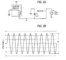
Figs. 2A and 2B are views explaining noise of a case where a diode is not used. -
Figs. 3A and 3B are views explaining noise of a case where a diode is used. -
Fig. 4 is a block diagram schematically showing another example of the circuit configuration of the field device according to the embodiment. -
Fig. 5 is a view showing a circuit having an inductor connected in series to a diode. -
Figs. 6A and 6B are views showing a circuit having a diode connected thereto to prevent an effective capacitance from being discharged. -
Figs. 7A and 7B are views schematically showing an impedance circuit including an effective capacitance by means of circuit blocks of an actual field device. - Embodiments of the present invention will be described with reference to the accompanying drawings.
Fig. 1 is a block diagram schematically showing a circuit configuration of afield device 100 according to the present embodiment. As shown in this figure, thefield device 100, which is connected to a two-wire loop wiring, has, as a main body portion, acurrent output circuit 110, a power supply circuit/control circuit 120 and asensor circuit 130, and also has, as a terminal portion, adiode 140, which is a rectifying element, and capacitors Ch and C1. Meanwhile, because this figure focuses on a common-mode noise mixed in the loop wiring, elements of a direct power supply system connected to the loop wiring are omitted. - The
current output circuit 110 controls a current to be flowed into the loop wiring. The power supply circuit/control circuit 120 includes a power supply circuit for supplying electric power, which has been supplied thereto through the loop wiring, to each circuit and a control circuit for calculating a signal from thesensor circuit 130 and determining a current to be flowed into the loop wiring. Impedance Za of thecurrent output circuit 110 is designated as Za and impedance of the power supply circuit/control circuit 120 is designated as Zb. - The capacitors Ch and Cl are capacitors for escaping a high frequency noise, which flows through the loop wiring, to the ground and are respectively connected to plus and minus sides. Specifically, the capacitor Ch is connected between the ground and a plus-side connection point between the terminal portion and the main body portion, and the capacitor Cl is connected between the ground and a minus-side connection point between the terminal portion and the main body portion.
- The
sensor circuit 130 is intended to measure a physical amount and transmit the physical amount to the power supply circuit/control circuit 120. Herein, thesensor circuit 130 is a grounding type in which a reference point thereof is grounded. Accordingly, impedance Zsh (plus side) and impedance Zsl (minus side) exist with respect to the ground due to stray capacitance and the like. - In the
field device 100, a parallel circuit, which is constituted of the power supply circuit/control circuit 120 and thesensor circuit 130, and thecurrent output circuit 110 are connected to the loop wiring via the terminal portion in a state that the parallel circuit and thecurrent output circuit 110 are connected to in series with each other, and thecurrent output circuit 110 is arranged on the plus side. - In the present embodiment, the
diode 140 is connected to only the minus side of terminal portion, in which thesensor circuit 130 is arranged. Specifically, thediode 140 is arranged on a wiring path in the terminal portion, which is directly connected with thesensor circuit 130. At this time, thediode 140 is connected to a noise generation side, rather than the capacitor C1. Namely, a noise rectified in thediode 140 is applied to the capacitor Cl. - If a common-mod noise Vn is mixed in the loop wiring of the
field device 100, with a regard to a path A, a noise component, which is divided by the impedance Za of thecurrent output circuit 110 and the plus-side impedance Zsh of thesensor circuit 130, of noise components, which cannot be removed by the capacitor Ch, is applied to the plus side of thesensor circuit 130. - Namely, when the noise applied to the plus side of the
sensor circuit 130 is designated as Vnoize, Vnoize is calculated as Vnoize≒Zsh/(Zsh+Za)·Vn. - The
current output circuit 110 is typically embodied as a current mirror circuit or a constant current circuit, and in general, Za is an impedance of about 100 kΩ, to10 kΩ. Also, because the plus-side impedance Zsh of thesensor circuit 130 is about 100 kΩ, the noise applied to thesensor circuit 130 becomes about 1/2 of the common mode noise, so that an influence of the noise on thesensor circuit 130 is relatively small. - With regard to a path B, a noise rectified by the
diode 140 and the capacitor C1 is applied to the minus side of thesensor circuit 130. Namely, with regard to both of the path A and the path B, noises are not directly applied to thesensor circuit 130. - For example, in a case where, as shown in
Fig. 2A , the common-mode noise Vn is 5 Vpp and 10 kHz and the capacitor Cl is 1 µF, when thediode 140 is not connected to the path B, a noise having an amplitude of 5V as shown inFig. 2B is applied to thesensor circuit 130, thereby causing a large noise current to be flowed therethrough. - Contrarily, when the
diode 140 is connected to the path B as shown inFig. 3A , an influence of the noise on thesensor circuit 130 becomes small because an alternating noise having a small amplitude as shown inFig. 3B is applied to thesensor circuit 130. - In the example of the figure, the common mode-noise Vn is 5 Vpp and 10 kHz, the capacitor Cl is 1 µF, and a saturation current of the
diode 140 is 100 nA. Because a forward current of thediode 140 is large, a charging time of the capacitor C is very short so that a greater part of a period thereof is a discharging time and thus a current flowing at this time becomes the saturation current. Because the frequency of the common-mode noise is 10 kHz, a time period, during which the saturation current flows, becomes generally 100 µs. A voltage change V in a capacitor when a constant current i flows through the capacitor during a time period of t is obtained as V=1/C·i·t, and therefore in this case, the noise amplitude is 0.15 V. - As described above, according to the
field device 100 of the present embodiment, a rectifying element is connected to only thesensor circuit 130 side of the terminal portion in an internal circuit thereof having thecurrent output circuit 110 and thesensor circuit 130 connected in series to each other. Accordingly, in one path, a noise divided by thesensor circuit 130 and thecurrent output circuit 110 is applied to thesensor circuit 130 and in the other path, a noise rectified by the rectifying element is applied to thesensor circuit 130, so that noise resistance of thefield device 100 can be enhanced without increasing the lowest operation voltage or increasing a withstand voltage of the internal circuit. The rectifying element may be constituted of a bipolar transistor or a CMOS transistor, instead of the diode. - Alternatively, although in the example shown in
Fig. 1 , thecurrent output circuit 110 is arranged on the plus side and thus thediode 140 is connected to the minus side of the terminal portion, as shown inFig. 4 , thediode 140 may be connected to the plus side of the terminal portion when thecurrent output circuit 110 is arranged on the minus side. Specifically, thediode 140 is arranged on a wiring path in the terminal portion, which is directly connected with thesensor circuit 130. - Also, as shown in
Fig. 5 , an inductor or a ferrite bead may be provided to be connected in series with thediode 140. Thus, a band in which noise can be reduced is widened so the noise resistance can be further enhanced. Specifically, a noise a having high frequency band is limited by the inductor and a noise having a frequency band lower than that is limited by thediode 140. In addition, by combining thediode 140 with the inductor, noise can be reduced without using a large inductor.
Claims (4)
- A field device comprising:a current output circuit;a sensor circuit; anda terminal portion including a rectifying element,wherein the current output circuit and the sensor circuit are connected a two-wire loop wiring via the terminal portion in a state that the current output circuit and the sensor circuit are connected in series with each other, andwherein the rectifying element is connected to only a sensor circuit side of the terminal portion.
- The field device according to claim 1, wherein the terminal portion comprises a grounded capacitor connected between the rectifying element and the sensor circuit.
- The field device according to claim 1 or 2, wherein the sensor circuit is a grounding type in which a reference point thereof is grounded.
- The field device according to any one of claims 1 to 3, wherein the terminal portion comprises an inductor connected in series with the rectifying element.
Applications Claiming Priority (1)
| Application Number | Priority Date | Filing Date | Title |
|---|---|---|---|
| JP2014182514A JP6237545B2 (en) | 2014-09-08 | 2014-09-08 | Field equipment |
Publications (2)
| Publication Number | Publication Date |
|---|---|
| EP3001153A1 true EP3001153A1 (en) | 2016-03-30 |
| EP3001153B1 EP3001153B1 (en) | 2017-11-29 |
Family
ID=54140230
Family Applications (1)
| Application Number | Title | Priority Date | Filing Date |
|---|---|---|---|
| EP15183911.5A Active EP3001153B1 (en) | 2014-09-08 | 2015-09-04 | Field device |
Country Status (4)
| Country | Link |
|---|---|
| US (1) | US10003327B2 (en) |
| EP (1) | EP3001153B1 (en) |
| JP (1) | JP6237545B2 (en) |
| CN (1) | CN105404342B (en) |
Citations (5)
| Publication number | Priority date | Publication date | Assignee | Title |
|---|---|---|---|---|
| DE2244677B1 (en) * | 1972-09-12 | 1974-03-28 | Hottinger Baldwin Messtechnik Gmbh, 6100 Darmstadt | ARRANGEMENT FOR ELECTRICAL MEASUREMENT OF MECHANICAL SIZES |
| DE2701184A1 (en) * | 1977-01-13 | 1978-07-27 | Endress Hauser Gmbh Co | CIRCUIT ARRANGEMENT FOR TRANSMISSION OF MEASURED VALUE SIGNALS |
| US4698586A (en) * | 1984-03-26 | 1987-10-06 | Pgep Professional General Electric Corp. | Electric particle detector for the detection of fire |
| WO1995034027A1 (en) | 1994-06-07 | 1995-12-14 | Rosemount Inc. | Transmitter with electrical circuitry for inhibiting discharge of stored energy |
| US20060033614A1 (en) * | 2004-08-14 | 2006-02-16 | Berend Kleen | Sensor with two electrical terminals |
Family Cites Families (10)
| Publication number | Priority date | Publication date | Assignee | Title |
|---|---|---|---|---|
| JPS53107387A (en) | 1977-02-28 | 1978-09-19 | Shimadzu Corp | Method and apparatus for eddy current non-destructive flaw detection |
| JPS5513749Y2 (en) * | 1978-08-04 | 1980-03-27 | ||
| CN1003099B (en) * | 1985-04-24 | 1989-01-18 | 布海维股份有限公司 | Particle electric detector for detecting fire |
| US5535243A (en) | 1994-07-13 | 1996-07-09 | Rosemount Inc. | Power supply for field mounted transmitter |
| US6292501B1 (en) * | 1998-09-10 | 2001-09-18 | Coherent, Inc. | Apparatus for reducing amplitude modulation of laser diode output |
| US7190102B2 (en) * | 2002-09-05 | 2007-03-13 | Viking Technologies, L.C. | Apparatus and method for charging and discharging a capacitor to a predetermined setpoint |
| JP4806563B2 (en) * | 2005-12-07 | 2011-11-02 | 株式会社東海理化電機製作所 | Current output type detector |
| JP4760608B2 (en) * | 2006-01-17 | 2011-08-31 | 株式会社デンソー | Drive control device for output transistor |
| CN201408014Y (en) | 2009-03-26 | 2010-02-17 | 南京奥联汽车电子电器有限公司 | Hall gear sensor |
| JP5673750B2 (en) * | 2012-11-12 | 2015-02-18 | 横河電機株式会社 | Current output circuit, and broadband two-wire transmitter having the same circuit |
-
2014
- 2014-09-08 JP JP2014182514A patent/JP6237545B2/en not_active Expired - Fee Related
-
2015
- 2015-09-03 US US14/844,451 patent/US10003327B2/en active Active
- 2015-09-04 EP EP15183911.5A patent/EP3001153B1/en active Active
- 2015-09-08 CN CN201510567484.2A patent/CN105404342B/en active Active
Patent Citations (5)
| Publication number | Priority date | Publication date | Assignee | Title |
|---|---|---|---|---|
| DE2244677B1 (en) * | 1972-09-12 | 1974-03-28 | Hottinger Baldwin Messtechnik Gmbh, 6100 Darmstadt | ARRANGEMENT FOR ELECTRICAL MEASUREMENT OF MECHANICAL SIZES |
| DE2701184A1 (en) * | 1977-01-13 | 1978-07-27 | Endress Hauser Gmbh Co | CIRCUIT ARRANGEMENT FOR TRANSMISSION OF MEASURED VALUE SIGNALS |
| US4698586A (en) * | 1984-03-26 | 1987-10-06 | Pgep Professional General Electric Corp. | Electric particle detector for the detection of fire |
| WO1995034027A1 (en) | 1994-06-07 | 1995-12-14 | Rosemount Inc. | Transmitter with electrical circuitry for inhibiting discharge of stored energy |
| US20060033614A1 (en) * | 2004-08-14 | 2006-02-16 | Berend Kleen | Sensor with two electrical terminals |
Also Published As
| Publication number | Publication date |
|---|---|
| CN105404342B (en) | 2017-10-20 |
| US10003327B2 (en) | 2018-06-19 |
| JP6237545B2 (en) | 2017-11-29 |
| US20160072489A1 (en) | 2016-03-10 |
| CN105404342A (en) | 2016-03-16 |
| JP2016057771A (en) | 2016-04-21 |
| EP3001153B1 (en) | 2017-11-29 |
Similar Documents
| Publication | Publication Date | Title |
|---|---|---|
| JP7418536B2 (en) | Wireless power receiving device, wireless power feeding device, wireless power transmission system, and excessive magnetic field protection method for wireless power receiving device | |
| CN105452882B (en) | Battery monitoring apparatus | |
| US9977455B2 (en) | Method and apparatus for filtering a rectified voltage | |
| US10128762B2 (en) | Semiconductor device for controlling power source | |
| US20140145732A1 (en) | Device for generating an alternating voltage difference between the reference potentials of electronic systems | |
| WO2018044515A1 (en) | Rectifier arbitration in wireless charging systems | |
| EP3361615A1 (en) | Switching regulator and control device therefor | |
| WO2015111380A1 (en) | Fuel-pressure sensor with built-in charge amplifier | |
| WO2014101861A1 (en) | Mutual-capacitance detection circuit and mutual-capacitance detection array | |
| KR101984548B1 (en) | Apparatus for detecting noise in Power Supply of PLC Analogue Input and Output Module | |
| US10365319B2 (en) | Apparatus for determining deterioration of photocoupler | |
| US20160322967A1 (en) | Circuit constant variable circuit | |
| EP3001153B1 (en) | Field device | |
| TWI540406B (en) | Voltage regulator and power receiving device | |
| JP6606038B2 (en) | Output voltage control circuit | |
| KR20160029675A (en) | Semiconductor apparatus and radio communication apparatus | |
| JP6366048B2 (en) | AC voltage detection circuit and power supply device including the same | |
| JP6725992B2 (en) | Wireless power transmission device and its control IC, abnormality detection method, charger | |
| JP5819226B2 (en) | Excitation circuit of electromagnetic flow meter | |
| ITTO20120919A1 (en) | CIRCUIT AND METHOD OF ADAPTATION OF THE ELECTRIC POWER SUPPLY FOR AN ENERGY COLLECTION SYSTEM | |
| JP5749211B2 (en) | Switching power supply device and switching power supply program writing system | |
| US11552625B2 (en) | Transmitting device for transmitting digital signals between galvanically isolated circuit parts, and field device having a transmitting device of this type | |
| JP2013183522A (en) | State monitor | |
| JP6435965B2 (en) | Input circuit and inverter device | |
| US9529023B2 (en) | Signal analysis circuit and signal analysis method thereof |
Legal Events
| Date | Code | Title | Description |
|---|---|---|---|
| PUAI | Public reference made under article 153(3) epc to a published international application that has entered the european phase |
Free format text: ORIGINAL CODE: 0009012 |
|
| AK | Designated contracting states |
Kind code of ref document: A1 Designated state(s): AL AT BE BG CH CY CZ DE DK EE ES FI FR GB GR HR HU IE IS IT LI LT LU LV MC MK MT NL NO PL PT RO RS SE SI SK SM TR |
|
| AX | Request for extension of the european patent |
Extension state: BA ME |
|
| 17P | Request for examination filed |
Effective date: 20160922 |
|
| RBV | Designated contracting states (corrected) |
Designated state(s): AL AT BE BG CH CY CZ DE DK EE ES FI FR GB GR HR HU IE IS IT LI LT LU LV MC MK MT NL NO PL PT RO RS SE SI SK SM TR |
|
| RIC1 | Information provided on ipc code assigned before grant |
Ipc: H03K 5/1252 20060101ALI20170516BHEP Ipc: G01D 3/08 20060101ALN20170516BHEP Ipc: G01D 21/00 20060101AFI20170516BHEP |
|
| GRAP | Despatch of communication of intention to grant a patent |
Free format text: ORIGINAL CODE: EPIDOSNIGR1 |
|
| INTG | Intention to grant announced |
Effective date: 20170627 |
|
| GRAS | Grant fee paid |
Free format text: ORIGINAL CODE: EPIDOSNIGR3 |
|
| GRAA | (expected) grant |
Free format text: ORIGINAL CODE: 0009210 |
|
| AK | Designated contracting states |
Kind code of ref document: B1 Designated state(s): AL AT BE BG CH CY CZ DE DK EE ES FI FR GB GR HR HU IE IS IT LI LT LU LV MC MK MT NL NO PL PT RO RS SE SI SK SM TR |
|
| REG | Reference to a national code |
Ref country code: CH Ref legal event code: EP |
|
| REG | Reference to a national code |
Ref country code: AT Ref legal event code: REF Ref document number: 950801 Country of ref document: AT Kind code of ref document: T Effective date: 20171215 |
|
| REG | Reference to a national code |
Ref country code: IE Ref legal event code: FG4D |
|
| REG | Reference to a national code |
Ref country code: DE Ref legal event code: R096 Ref document number: 602015006292 Country of ref document: DE |
|
| REG | Reference to a national code |
Ref country code: NL Ref legal event code: MP Effective date: 20171129 |
|
| REG | Reference to a national code |
Ref country code: LT Ref legal event code: MG4D |
|
| REG | Reference to a national code |
Ref country code: AT Ref legal event code: MK05 Ref document number: 950801 Country of ref document: AT Kind code of ref document: T Effective date: 20171129 |
|
| PG25 | Lapsed in a contracting state [announced via postgrant information from national office to epo] |
Ref country code: NO Free format text: LAPSE BECAUSE OF FAILURE TO SUBMIT A TRANSLATION OF THE DESCRIPTION OR TO PAY THE FEE WITHIN THE PRESCRIBED TIME-LIMIT Effective date: 20180228 Ref country code: FI Free format text: LAPSE BECAUSE OF FAILURE TO SUBMIT A TRANSLATION OF THE DESCRIPTION OR TO PAY THE FEE WITHIN THE PRESCRIBED TIME-LIMIT Effective date: 20171129 Ref country code: SE Free format text: LAPSE BECAUSE OF FAILURE TO SUBMIT A TRANSLATION OF THE DESCRIPTION OR TO PAY THE FEE WITHIN THE PRESCRIBED TIME-LIMIT Effective date: 20171129 Ref country code: ES Free format text: LAPSE BECAUSE OF FAILURE TO SUBMIT A TRANSLATION OF THE DESCRIPTION OR TO PAY THE FEE WITHIN THE PRESCRIBED TIME-LIMIT Effective date: 20171129 Ref country code: LT Free format text: LAPSE BECAUSE OF FAILURE TO SUBMIT A TRANSLATION OF THE DESCRIPTION OR TO PAY THE FEE WITHIN THE PRESCRIBED TIME-LIMIT Effective date: 20171129 |
|
| PG25 | Lapsed in a contracting state [announced via postgrant information from national office to epo] |
Ref country code: GR Free format text: LAPSE BECAUSE OF FAILURE TO SUBMIT A TRANSLATION OF THE DESCRIPTION OR TO PAY THE FEE WITHIN THE PRESCRIBED TIME-LIMIT Effective date: 20180301 Ref country code: AT Free format text: LAPSE BECAUSE OF FAILURE TO SUBMIT A TRANSLATION OF THE DESCRIPTION OR TO PAY THE FEE WITHIN THE PRESCRIBED TIME-LIMIT Effective date: 20171129 Ref country code: LV Free format text: LAPSE BECAUSE OF FAILURE TO SUBMIT A TRANSLATION OF THE DESCRIPTION OR TO PAY THE FEE WITHIN THE PRESCRIBED TIME-LIMIT Effective date: 20171129 Ref country code: BG Free format text: LAPSE BECAUSE OF FAILURE TO SUBMIT A TRANSLATION OF THE DESCRIPTION OR TO PAY THE FEE WITHIN THE PRESCRIBED TIME-LIMIT Effective date: 20180228 Ref country code: RS Free format text: LAPSE BECAUSE OF FAILURE TO SUBMIT A TRANSLATION OF THE DESCRIPTION OR TO PAY THE FEE WITHIN THE PRESCRIBED TIME-LIMIT Effective date: 20171129 Ref country code: HR Free format text: LAPSE BECAUSE OF FAILURE TO SUBMIT A TRANSLATION OF THE DESCRIPTION OR TO PAY THE FEE WITHIN THE PRESCRIBED TIME-LIMIT Effective date: 20171129 |
|
| PG25 | Lapsed in a contracting state [announced via postgrant information from national office to epo] |
Ref country code: NL Free format text: LAPSE BECAUSE OF FAILURE TO SUBMIT A TRANSLATION OF THE DESCRIPTION OR TO PAY THE FEE WITHIN THE PRESCRIBED TIME-LIMIT Effective date: 20171129 |
|
| PG25 | Lapsed in a contracting state [announced via postgrant information from national office to epo] |
Ref country code: CZ Free format text: LAPSE BECAUSE OF FAILURE TO SUBMIT A TRANSLATION OF THE DESCRIPTION OR TO PAY THE FEE WITHIN THE PRESCRIBED TIME-LIMIT Effective date: 20171129 Ref country code: CY Free format text: LAPSE BECAUSE OF FAILURE TO SUBMIT A TRANSLATION OF THE DESCRIPTION OR TO PAY THE FEE WITHIN THE PRESCRIBED TIME-LIMIT Effective date: 20171129 Ref country code: DK Free format text: LAPSE BECAUSE OF FAILURE TO SUBMIT A TRANSLATION OF THE DESCRIPTION OR TO PAY THE FEE WITHIN THE PRESCRIBED TIME-LIMIT Effective date: 20171129 Ref country code: EE Free format text: LAPSE BECAUSE OF FAILURE TO SUBMIT A TRANSLATION OF THE DESCRIPTION OR TO PAY THE FEE WITHIN THE PRESCRIBED TIME-LIMIT Effective date: 20171129 Ref country code: SK Free format text: LAPSE BECAUSE OF FAILURE TO SUBMIT A TRANSLATION OF THE DESCRIPTION OR TO PAY THE FEE WITHIN THE PRESCRIBED TIME-LIMIT Effective date: 20171129 |
|
| REG | Reference to a national code |
Ref country code: DE Ref legal event code: R097 Ref document number: 602015006292 Country of ref document: DE |
|
| PG25 | Lapsed in a contracting state [announced via postgrant information from national office to epo] |
Ref country code: IT Free format text: LAPSE BECAUSE OF FAILURE TO SUBMIT A TRANSLATION OF THE DESCRIPTION OR TO PAY THE FEE WITHIN THE PRESCRIBED TIME-LIMIT Effective date: 20171129 Ref country code: SM Free format text: LAPSE BECAUSE OF FAILURE TO SUBMIT A TRANSLATION OF THE DESCRIPTION OR TO PAY THE FEE WITHIN THE PRESCRIBED TIME-LIMIT Effective date: 20171129 Ref country code: RO Free format text: LAPSE BECAUSE OF FAILURE TO SUBMIT A TRANSLATION OF THE DESCRIPTION OR TO PAY THE FEE WITHIN THE PRESCRIBED TIME-LIMIT Effective date: 20171129 Ref country code: PL Free format text: LAPSE BECAUSE OF FAILURE TO SUBMIT A TRANSLATION OF THE DESCRIPTION OR TO PAY THE FEE WITHIN THE PRESCRIBED TIME-LIMIT Effective date: 20171129 |
|
| PLBE | No opposition filed within time limit |
Free format text: ORIGINAL CODE: 0009261 |
|
| STAA | Information on the status of an ep patent application or granted ep patent |
Free format text: STATUS: NO OPPOSITION FILED WITHIN TIME LIMIT |
|
| 26N | No opposition filed |
Effective date: 20180830 |
|
| PG25 | Lapsed in a contracting state [announced via postgrant information from national office to epo] |
Ref country code: SI Free format text: LAPSE BECAUSE OF FAILURE TO SUBMIT A TRANSLATION OF THE DESCRIPTION OR TO PAY THE FEE WITHIN THE PRESCRIBED TIME-LIMIT Effective date: 20171129 |
|
| PG25 | Lapsed in a contracting state [announced via postgrant information from national office to epo] |
Ref country code: MC Free format text: LAPSE BECAUSE OF FAILURE TO SUBMIT A TRANSLATION OF THE DESCRIPTION OR TO PAY THE FEE WITHIN THE PRESCRIBED TIME-LIMIT Effective date: 20171129 |
|
| REG | Reference to a national code |
Ref country code: CH Ref legal event code: PL |
|
| REG | Reference to a national code |
Ref country code: BE Ref legal event code: MM Effective date: 20180930 |
|
| REG | Reference to a national code |
Ref country code: IE Ref legal event code: MM4A |
|
| PG25 | Lapsed in a contracting state [announced via postgrant information from national office to epo] |
Ref country code: LU Free format text: LAPSE BECAUSE OF NON-PAYMENT OF DUE FEES Effective date: 20180904 |
|
| PG25 | Lapsed in a contracting state [announced via postgrant information from national office to epo] |
Ref country code: IE Free format text: LAPSE BECAUSE OF NON-PAYMENT OF DUE FEES Effective date: 20180904 |
|
| PG25 | Lapsed in a contracting state [announced via postgrant information from national office to epo] |
Ref country code: CH Free format text: LAPSE BECAUSE OF NON-PAYMENT OF DUE FEES Effective date: 20180930 Ref country code: LI Free format text: LAPSE BECAUSE OF NON-PAYMENT OF DUE FEES Effective date: 20180930 Ref country code: FR Free format text: LAPSE BECAUSE OF NON-PAYMENT OF DUE FEES Effective date: 20180930 Ref country code: BE Free format text: LAPSE BECAUSE OF NON-PAYMENT OF DUE FEES Effective date: 20180930 |
|
| PG25 | Lapsed in a contracting state [announced via postgrant information from national office to epo] |
Ref country code: MT Free format text: LAPSE BECAUSE OF NON-PAYMENT OF DUE FEES Effective date: 20180904 |
|
| PG25 | Lapsed in a contracting state [announced via postgrant information from national office to epo] |
Ref country code: TR Free format text: LAPSE BECAUSE OF FAILURE TO SUBMIT A TRANSLATION OF THE DESCRIPTION OR TO PAY THE FEE WITHIN THE PRESCRIBED TIME-LIMIT Effective date: 20171129 |
|
| PG25 | Lapsed in a contracting state [announced via postgrant information from national office to epo] |
Ref country code: PT Free format text: LAPSE BECAUSE OF FAILURE TO SUBMIT A TRANSLATION OF THE DESCRIPTION OR TO PAY THE FEE WITHIN THE PRESCRIBED TIME-LIMIT Effective date: 20171129 |
|
| PG25 | Lapsed in a contracting state [announced via postgrant information from national office to epo] |
Ref country code: HU Free format text: LAPSE BECAUSE OF FAILURE TO SUBMIT A TRANSLATION OF THE DESCRIPTION OR TO PAY THE FEE WITHIN THE PRESCRIBED TIME-LIMIT; INVALID AB INITIO Effective date: 20150904 Ref country code: MK Free format text: LAPSE BECAUSE OF NON-PAYMENT OF DUE FEES Effective date: 20171129 |
|
| PG25 | Lapsed in a contracting state [announced via postgrant information from national office to epo] |
Ref country code: AL Free format text: LAPSE BECAUSE OF FAILURE TO SUBMIT A TRANSLATION OF THE DESCRIPTION OR TO PAY THE FEE WITHIN THE PRESCRIBED TIME-LIMIT Effective date: 20171129 Ref country code: IS Free format text: LAPSE BECAUSE OF FAILURE TO SUBMIT A TRANSLATION OF THE DESCRIPTION OR TO PAY THE FEE WITHIN THE PRESCRIBED TIME-LIMIT Effective date: 20180329 |
|
| GBPC | Gb: european patent ceased through non-payment of renewal fee |
Effective date: 20190904 |
|
| PG25 | Lapsed in a contracting state [announced via postgrant information from national office to epo] |
Ref country code: GB Free format text: LAPSE BECAUSE OF NON-PAYMENT OF DUE FEES Effective date: 20190904 |
|
| P01 | Opt-out of the competence of the unified patent court (upc) registered |
Effective date: 20230603 |
|
| PGFP | Annual fee paid to national office [announced via postgrant information from national office to epo] |
Ref country code: DE Payment date: 20240820 Year of fee payment: 10 |