EP2999118A1 - Gate control device, semiconductor device, and method for controlling semiconductor device - Google Patents
Gate control device, semiconductor device, and method for controlling semiconductor device Download PDFInfo
- Publication number
- EP2999118A1 EP2999118A1 EP15179431.0A EP15179431A EP2999118A1 EP 2999118 A1 EP2999118 A1 EP 2999118A1 EP 15179431 A EP15179431 A EP 15179431A EP 2999118 A1 EP2999118 A1 EP 2999118A1
- Authority
- EP
- European Patent Office
- Prior art keywords
- voltage
- threshold voltage
- gate
- difference
- transistor
- Prior art date
- Legal status (The legal status is an assumption and is not a legal conclusion. Google has not performed a legal analysis and makes no representation as to the accuracy of the status listed.)
- Granted
Links
Images





Classifications
-
- H—ELECTRICITY
- H03—ELECTRONIC CIRCUITRY
- H03K—PULSE TECHNIQUE
- H03K17/00—Electronic switching or gating, i.e. not by contact-making and –breaking
- H03K17/51—Electronic switching or gating, i.e. not by contact-making and –breaking characterised by the components used
- H03K17/56—Electronic switching or gating, i.e. not by contact-making and –breaking characterised by the components used by the use, as active elements, of semiconductor devices
- H03K17/687—Electronic switching or gating, i.e. not by contact-making and –breaking characterised by the components used by the use, as active elements, of semiconductor devices the devices being field-effect transistors
-
- H—ELECTRICITY
- H03—ELECTRONIC CIRCUITRY
- H03K—PULSE TECHNIQUE
- H03K17/00—Electronic switching or gating, i.e. not by contact-making and –breaking
- H03K17/04—Modifications for accelerating switching
- H03K17/041—Modifications for accelerating switching without feedback from the output circuit to the control circuit
- H03K17/0412—Modifications for accelerating switching without feedback from the output circuit to the control circuit by measures taken in the control circuit
- H03K17/04123—Modifications for accelerating switching without feedback from the output circuit to the control circuit by measures taken in the control circuit in field-effect transistor switches
-
- H—ELECTRICITY
- H03—ELECTRONIC CIRCUITRY
- H03K—PULSE TECHNIQUE
- H03K17/00—Electronic switching or gating, i.e. not by contact-making and –breaking
- H03K17/06—Modifications for ensuring a fully conducting state
- H03K17/063—Modifications for ensuring a fully conducting state in field-effect transistor switches
-
- H—ELECTRICITY
- H03—ELECTRONIC CIRCUITRY
- H03K—PULSE TECHNIQUE
- H03K17/00—Electronic switching or gating, i.e. not by contact-making and –breaking
- H03K17/16—Modifications for eliminating interference voltages or currents
- H03K17/161—Modifications for eliminating interference voltages or currents in field-effect transistor switches
- H03K17/162—Modifications for eliminating interference voltages or currents in field-effect transistor switches without feedback from the output circuit to the control circuit
- H03K17/163—Soft switching
-
- H—ELECTRICITY
- H10—SEMICONDUCTOR DEVICES; ELECTRIC SOLID-STATE DEVICES NOT OTHERWISE PROVIDED FOR
- H10D—INORGANIC ELECTRIC SEMICONDUCTOR DEVICES
- H10D30/00—Field-effect transistors [FET]
- H10D30/40—FETs having zero-dimensional [0D], one-dimensional [1D] or two-dimensional [2D] charge carrier gas channels
- H10D30/47—FETs having zero-dimensional [0D], one-dimensional [1D] or two-dimensional [2D] charge carrier gas channels having two-dimensional [2D] charge carrier gas channels, e.g. nanoribbon FETs or high electron mobility transistors [HEMT]
- H10D30/471—High electron mobility transistors [HEMT] or high hole mobility transistors [HHMT]
- H10D30/475—High electron mobility transistors [HEMT] or high hole mobility transistors [HHMT] having wider bandgap layer formed on top of lower bandgap active layer, e.g. undoped barrier HEMTs such as i-AlGaN/GaN HEMTs
-
- H—ELECTRICITY
- H10—SEMICONDUCTOR DEVICES; ELECTRIC SOLID-STATE DEVICES NOT OTHERWISE PROVIDED FOR
- H10D—INORGANIC ELECTRIC SEMICONDUCTOR DEVICES
- H10D30/00—Field-effect transistors [FET]
- H10D30/40—FETs having zero-dimensional [0D], one-dimensional [1D] or two-dimensional [2D] charge carrier gas channels
- H10D30/47—FETs having zero-dimensional [0D], one-dimensional [1D] or two-dimensional [2D] charge carrier gas channels having two-dimensional [2D] charge carrier gas channels, e.g. nanoribbon FETs or high electron mobility transistors [HEMT]
- H10D30/471—High electron mobility transistors [HEMT] or high hole mobility transistors [HHMT]
- H10D30/475—High electron mobility transistors [HEMT] or high hole mobility transistors [HHMT] having wider bandgap layer formed on top of lower bandgap active layer, e.g. undoped barrier HEMTs such as i-AlGaN/GaN HEMTs
- H10D30/4755—High electron mobility transistors [HEMT] or high hole mobility transistors [HHMT] having wider bandgap layer formed on top of lower bandgap active layer, e.g. undoped barrier HEMTs such as i-AlGaN/GaN HEMTs having wide bandgap charge-carrier supplying layers, e.g. modulation doped HEMTs such as n-AlGaAs/GaAs HEMTs
-
- H—ELECTRICITY
- H10—SEMICONDUCTOR DEVICES; ELECTRIC SOLID-STATE DEVICES NOT OTHERWISE PROVIDED FOR
- H10D—INORGANIC ELECTRIC SEMICONDUCTOR DEVICES
- H10D62/00—Semiconductor bodies, or regions thereof, of devices having potential barriers
- H10D62/80—Semiconductor bodies, or regions thereof, of devices having potential barriers characterised by the materials
- H10D62/85—Semiconductor bodies, or regions thereof, of devices having potential barriers characterised by the materials being Group III-V materials, e.g. GaAs
- H10D62/8503—Nitride Group III-V materials, e.g. AlN or GaN
-
- H—ELECTRICITY
- H03—ELECTRONIC CIRCUITRY
- H03K—PULSE TECHNIQUE
- H03K2217/00—Indexing scheme related to electronic switching or gating, i.e. not by contact-making or -breaking covered by H03K17/00
- H03K2217/0036—Means reducing energy consumption
-
- H—ELECTRICITY
- H10—SEMICONDUCTOR DEVICES; ELECTRIC SOLID-STATE DEVICES NOT OTHERWISE PROVIDED FOR
- H10D—INORGANIC ELECTRIC SEMICONDUCTOR DEVICES
- H10D62/00—Semiconductor bodies, or regions thereof, of devices having potential barriers
- H10D62/10—Shapes, relative sizes or dispositions of the regions of the semiconductor bodies; Shapes of the semiconductor bodies
- H10D62/17—Semiconductor regions connected to electrodes not carrying current to be rectified, amplified or switched, e.g. channel regions
- H10D62/343—Gate regions of field-effect devices having PN junction gates
Definitions
- Embodiments described herein relate generally to a gate control device, a semiconductor device, and a method for controlling the semiconductor device.
- GaN gallium nitride
- Si silicon
- a High Electron Mobility Transistor (HEMT) structure using a two dimensional electron gas (2DEG) as the carrier is widely applied to a GaN based transistor.
- a junction HEMT is one type of GaN based HEMTs.
- a p-type GaN based semiconductor for a gate electrode in a junction HEMT can achieve the normally off operation. Meanwhile, injecting a positive hole (hole) from the gate electrode to a channel causes conductivity modulation. This can reduce the on-resistance of the junction HEMT. However, the injection of a hole unfortunately increases the switching time of the junction HEMT.
- a gate control device of an embodiment is configured to control a gate voltage to be applied to a gate electrode of a junction field effect transistor including a source electrode, a drain electrode, and the gate electrode, the transistor having a first threshold voltage at which the transistor is turned on, and a second threshold voltage at which conductivity modulation occurs in the transistor so as to make the gate voltage equal to or higher than the second threshold voltage when a forward current in a direction from the drain electrode toward the source electrode flows, and so as to make a time variation in the gate voltage have a point from which a rate of the time variation starts decreasing at a voltage between the second threshold voltage and the first threshold voltage when the forward current to be shut down.
- the semiconductor device may be a power module that is a combination of a plurality of elements such as a discrete semiconductor.
- the semiconductor device may be an intelligent power module formed by a plurality of elements such as a discrete semiconductor in which a drive circuit configured to drive the elements or a self-protection function is embedded.
- the semiconductor device may be an entire system including a power module or an intelligent power module.
- GaN gallium nitride
- AlN aluminum nitride
- InN indium nitride
- GaN based semiconductor semiconductors including gallium nitride (GaN), aluminum nitride (AlN), indium nitride (InN), and their intermediate compositions are collectively referred to as a "GaN based semiconductor”.
- a "gate voltage” and a “drain voltage” mean voltages based on a "source voltage”.
- a semiconductor device includes: a junction field effect transistor including a source electrode, a drain electrode, and a gate electrode, and further including and further including a first threshold voltage at which the transistor is turned on and a current starts flowing between the source electrode and the drain electrode, and a second threshold voltage at which conductivity modulation occurs in the transistor and a current starts flowing between the source electrode and the gate electrode; and a gate control device configured to control a gate voltage to be applied to the gate electrode so as to make the gate voltage equal to or higher than the second threshold voltage when a forward current in a direction from the drain electrode toward the source electrode flows, and so as to make a time variation in the gate voltage have a point from which the rate of the time variation starts decreasing at a voltage between the second threshold voltage and the first threshold voltage when the forward current is shut down.
- FIGS. 1A and 1B are circuit diagrams of the primary components of the semiconductor device according to the present embodiment.
- the semiconductor device according to the present embodiment is, for example, an intelligent power module including an inverter circuit.
- FIGS. 1A and 1B are diagrams of a switching unit included in the inverter circuit.
- FIG. 1A is a circuit diagram of the entire switching unit
- FIG. 1B is a circuit diagram of an exemplary delay circuit in the switching unit.
- the semiconductor device includes a GaN based HEMT 10 that is an exemplary junction field effect transistor (JFET), and a gate drive circuit 20 that is an exemplary gate control device.
- JFET junction field effect transistor
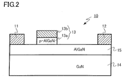
- FIG. 2 is a schematic cross-sectional view of the junction field effect transistor according to the present embodiment.
- the GaN based HEMT 10 is a normally off transistor.
- the GaN based HEMT 10 includes a GaN channel layer 14, an AlGaN barrier layer 15, a source electrode 11, a drain electrode 12, and a gate electrode 13.
- the source electrode 11 and the drain electrode 12 are, for example, metal.
- the gate electrode 13 has, for example, a stacked structure with a p-type AlGaN capping layer 13a and a metallic layer 13b.
- FIGS. 3A and 3B are explanatory diagrams of the operation of the junction field effect transistor according to the present embodiment.
- Two dimensional electron gas (2DEG) is induced on the interface of the GaN channel layer 14 and the AlGaN barrier layer 15 in the GaN based HEMT 10.
- a voltage equal to or higher than a first threshold voltage (Vth 1 ) is applied as a gate voltage to the gate electrode 13
- the transistor is turned on.
- a current starts flowing between the source electrode 11 and the drain electrode 12 ( FIG. 3A ).
- a current flowing in a direction from the drain electrode 12 to the source electrode 11 is referred to as a forward current
- a current flowing in a direction from the source electrode 11 to the drain electrode 12 is referred to as a reverse current.
- FIGS. 3A and 3B illustrates that the forward current flows. Note that the direction of current is opposite to flow direction of electron.
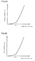
- FIGS. 4A and 4B are explanatory diagrams of the threshold voltages of the junction field effect transistor according to the present embodiment.
- FIG. 4A is a diagram of the definition of the first threshold voltage (Vth 1 ) and
- FIG. 4B is a diagram of the definition of the second threshold voltage (Vth 2 ).
- the first threshold voltage (Vth 1 ) at which the transistor is turned on is defined as the value of the x-axis intercept when the tangent to the curve of current and voltage has the largest gradient while the gate voltage is shown on the X axis and the drain current is shown on the Y axis.
- the source electrode 11, the drain electrode 12, and the gate electrode 13 are connected to the source terminal 100, the drain terminal 200, and the gate terminal 300, respectively, in the GaN based HEMT 10.
- the drain terminal 200 is connected, for example, to an inductive load such as a motor.
- the gate drive circuit 20 includes: a power source terminal 21a to which a power source for high gate voltage (Vg H ) is connected; a power source terminal 21b to which a power source for low gate voltage (Vg L ) is connected; switch circuits 22a, 22b, and 22c; resistance elements 23a and 23b; an XOR circuit 24; a NOR circuit 25; a delay circuit 26; and a terminal 27 at a potential equal to the potential of the source terminal 100 or a potential lower than the potential of the source terminal 100.
- FIG. 1B illustrates an example of the delay circuit 26.
- the gate drive circuit 20 is connected to a gate drive signal generation source 30.
- the gate drive circuit 20 controls the gate voltage of the GaN based HEMT 10 in accordance with on and off signals input from the gate drive signal generation source 30.
- the gate drive circuit 20 has a function of controlling the gate voltage so as to make the gate voltage equal to or higher than the second threshold voltage (Vth 2 ) when the forward current in the direction from the drain electrode 12 toward the source electrode 11 flows, and controlling the gate voltage so as to make the time variation in gate voltage have a point from which the rate of the time variation starts decreasing at a voltage between the second threshold voltage (Vth 2 ) and the first threshold voltage (Vth 1 ) when the forward current to be shut down.
- the method for controlling the semiconductor device is used to control the gate voltage so as to make the gate voltage equal to or higher than the second threshold voltage when the forward current flows from the drain electrode toward the source electrode.
- the gate voltage is applied to the gate electrode of the junction field effect transistor including the source electrode, the drain electrode, and the gate electrode, and having the first threshold voltage at which a current starts flowing between the source electrode and the drain electrode, and the second threshold voltage at which a current starts flowing between the source electrode and the gate electrode.
- the method is used to control the gate voltage so as to make the time variation in gate voltage have a point from which the rate of the time variation starts decreasing at a voltage between the second threshold voltage and the first threshold voltage when the forward current to be shut down.
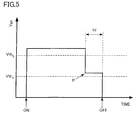
- FIG. 5 is an explanatory diagram of an exemplary method for controlling the semiconductor device according to the present embodiment. The time is shown on the horizontal axis, and the gate voltage (Vgs) applied to the gate electrode 13 of the GaN based HEMT 10 illustrated in FIG. 1A is shown on the vertical axis.
- Vgs gate voltage
- the gate drive circuit 20 controls the gate voltage so as to make the gate voltage equal to or higher than the second threshold voltage (Vth 2 ).
- the gate voltage equal to or higher than the second threshold voltage (Vth 2 ) injects a hole to the channel layer 14, and thus causes the conductivity modulation. This maintains a low on-resistance of the GaN based HEMT 10.
- the gate drive circuit 20 controls the gate voltage so as to make the time variation in gate voltage have a point from which the rate of the time variation starts decreasing at a voltage between the second threshold voltage (Vth 2 ) and the first threshold voltage ((Vth 1 ) (a point P in FIG. 5 ). Subsequently, the gate drive circuit 20 controls the gate voltage so as to make the gate voltage lower than the first threshold voltage (Vth 1 ).
- FIG. 5 illustrates that the gate drive circuit 20 controls the gate voltage so as to vary the gate voltage in a staircase pattern and maintain the gate voltage at a constant voltage between the second threshold voltage (Vth 2 ) and the first threshold voltage (Vth 1 ) for a predetermined time (td).
- the rate of time variation in gate voltage becomes zero at the point P.
- a voltage (Vg H ) equal to or higher than the second threshold voltage (Vth 2 ) is supplied from the power source terminal 21a, and a voltage (Vg L )between the second threshold voltage (Vth 2 ) and the first threshold voltage (Vth 1 ) is supplied from the power source terminal 21b.
- FIG. 6 is an explanatory diagram of another exemplary method for controlling the semiconductor device according to the present embodiment. The time is shown on the horizontal axis, and the gate voltage applied to the gate electrode 13 of the GaN based HEMT 10 illustrated in FIG. 1A is shown on the vertical axis.
- the gate voltage is gradually reduced when the GaN based HEMT 10 is turned off in FIG. 6 .
- the gate voltage is controlled such that the time variation in gate voltage has a point from which the rate of the time variation starts decreasing at a voltage between the second threshold voltage (Vth 2 ) and the first threshold voltage ((Vth 1 ) (a point P in FIG. 6 ).
- the gate voltage is maintained at a voltage between the second threshold voltage (Vth 2 ) and the first threshold voltage (Vth 1 ) for a predetermined time (td).
- the gate voltage is controlled such that a curve of time and voltage has an inflection point protruding downward between the second threshold voltage (Vth 2 ) and the first threshold voltage (Vth 1 ).
- FIG. 7 is an explanatory diagram of an exemplary method for controlling the semiconductor device according to a comparative embodiment. The time is shown on the horizontal axis, and a gate voltage (Vgs) to be applied to a gate electrode of a GaN based HEMT is shown on the vertical axis.
- Vgs gate voltage
- the gate voltage is controlled such that the gate voltage is equal to or higher than a second threshold voltage (Vth 2 ) in the comparative embodiment when the GaN based HEMT is turned on.
- Vth 2 a second threshold voltage
- the gate voltage is linearly reduced to zero when the GaN based HEMT is turned off.
- the hole injected into the channel layer remains after the gate voltage decreases to zero.
- the drain current continues flowing until the hole disappears. This unfortunately elongates the switching time.
- the gate drive circuit 20 controls the gate voltage so as to make the time variation in gate voltage have a point from which the rate of the time variation starts decreasing at a voltage between the second threshold voltage (Vth 2 ) and the first threshold voltage ((Vth 1 ) (the points P in FIGS. 5 and 6 ).
- This control maintains the state in which the transistor is on without the injection of a hole for a predetermined time (td) until the time when the gate voltage becomes zero.
- Providing a period of time in which a hole is not injected causes the hole in the channel layer 14 to disappear in the period. This can reduce the switching time of the GaN based HEMT 10.
- FIG. 8 illustrates the waveforms of the actual measurement of the operation of the semiconductor device according to the comparative embodiment.
- the gate voltage is reduced to a negative voltage.
- the hole can remain in the channel layer at least for the period of 18 nanoseconds.
- the predetermined time (td) in which the gate voltage is maintained at a voltage between the second threshold voltage (Vth 2 ) and the first threshold voltage (Vth 1 ) is preferably equal to or longer than 18 nanoseconds in the present embodiment.
- the semiconductor device according to the present embodiment is controlled in the following manner in the method for controlling the semiconductor device according to the present embodiment.
- the semiconductor device is controlled such that the difference between the gate voltage and the drain voltage is equal to or higher than the second threshold voltage.
- the semiconductor device is controlled such that the time variation in difference between the gate voltage and the drain voltage has a point from which the rate of the time variation starts decreasing at a voltage between the second threshold voltage and the first threshold voltage and the difference between the gate voltage and the drain voltage is subsequently kept equal to or lower than the first threshold voltage.
- the case in which the reverse current in the direction from the source electrode toward the drain electrode flows is, for example, the case in which the semiconductor device is a switching unit including an inverter circuit and a return current flows in the GaN based HEMT 10.
- the semiconductor device is a switching unit including an inverter circuit and a return current flows in the GaN based HEMT 10.
- the case in which a relatively positive voltage is applied to the source terminal 100 and a relatively negative voltage is applied to the drain terminal 200 in FIGS. 1A and 1B .
- FIGS. 9A and 9B are explanatory diagrams of the operation of the junction field effect transistor according to the first embodiment. The operation for causing the reverse current in the direction from the source electrode 11 toward the drain electrode 12 to flow will be described. When the reverse current flows, the voltage of the source electrode 11 is relatively higher than that of the drain electrode 12.
- Two dimensional electron gas (2DEG) is induced on the interface between the GaN channel layer 14 and the AlGaN barrier layer 15 in the GaN based HEMT 10.
- 2DEG Two dimensional electron gas
- FIGS. 9A and 9B illustrates that the reverse current flows.
- the conductivity modulation occurs. This reduces the on-resistance of the GaN based HEMT 10 ( FIG. 9B ).
- the gate drive circuit 20 preferably includes a function of controlling the gate voltage in the following manner.
- the gate drive circuit 20 controls the difference between the gate voltage and the drain voltage so as to make the difference between the gate voltage and the drain voltage equal to or higher than the second threshold voltage (Vth 2 ).
- the gate drive circuit 20 controls the difference between the gate voltage and the drain voltage so as to make the time variation in difference between the gate voltage and the drain voltage have a point from which the rate of the time variation starts decreasing at a voltage between the second threshold voltage (Vth 2 ) and the first threshold voltage (Vth 1 ), and so as to subsequently keep the difference between the gate voltage and the drain voltage equal to or lower than the first threshold voltage (Vth 1 ).
- the semiconductor device is preferably controlled in the following manner in the method for controlling the semiconductor device according to the first embodiment.
- the semiconductor device is controlled such that the difference between the gate voltage and the drain voltage is equal to or higher than the second threshold voltage (Vth 2 ).
- the semiconductor device is controlled such that the time variation in difference between the gate voltage and the drain voltage has a point from which the rate of the time variation starts decreasing at a voltage between the second threshold voltage (Vth 2 ) and the first threshold voltage (Vth 1 ), and the difference between the gate voltage and the drain voltage is kept equal to or lower than the first threshold voltage (Vth 1 ).
- FIG. 10 is an explanatory diagram of an exemplary method for controlling the semiconductor device according to the present embodiment.
- the upper graph illustrates the time on the horizontal axis and the difference between the gate voltage and the drain voltage (Vgs - Vds) applied to the gate electrode 13 and the drain electrode 12 of the GaN based HEMT 10 illustrated in FIG. 1 on the vertical axis.
- the lower graph illustrates the reverse current flowing in the GaN based HEMT 10.
- a return current flows in the GaN based HEMT 10 during a return flow period.
- the reverse current flows.
- the operation of the inverter circuit determines the return flow period.
- the on-resistance of the GaN based HEMT 10 is reduced and thus the loss is reduced for a predetermined period of time in the return flow period.
- the period is referred to as a synchronous rectification period. If the return flow period is in agreement with the synchronous rectification period, a short circuit may unfortunately occur in the inverter circuit. Thus, a time lag is generally provided between the return flow period and the synchronous rectification period.
- a time lag before the completion of the return flow period is referred to as a second predetermined time (tdr 2 ).
- the hole remains in the channel layer even after the difference between the gate voltage and the drain voltage becomes zero.
- the second predetermined time (tdr 2 ) is short, the reverse recovery current flows in the GaN based HEMT 10 even after the completion of the return flow period. This may unfortunately cause a short circuit in the inverter circuit.
- the difference between the gate voltage and the drain voltage is controlled such that the time variation in difference between the gate voltage and the drain voltage has a point at which the rate of the time variation starts decreasing at a voltage between the second threshold voltage (Vth 2 ) and the first threshold voltage ((Vth 1 ) (a point P in the upper graph in FIG. 10 ), and the difference between the gate voltage and the drain voltage is subsequently kept equal to or lower than the first threshold voltage (Vth 1 ).
- Providing a period of time in which a hole is not injected causes the hole in the channel layer 14 to disappear in the period. This can prevent the reverse recovery current from flowing in the GaN based HEMT 10 and thus can prevent a short circuit from occurring in the inverter circuit.
- the difference between the gate voltage and the drain voltage is controlled in the following manner in the example of FIG. 10 .
- the difference between the gate voltage and the drain voltage is reduced from the second threshold voltage (Vth 2 ) while varying in a staircase pattern, the difference between the gate voltage and the drain voltage is controlled such that the difference is maintained at a constant voltage between the second threshold voltage (Vth 2 ) and the first threshold voltage for the first predetermined time (tdr 1 ).
- the difference between the gate voltage and the drain voltage is kept lower than the first threshold voltage ((Vth 1 ) for the second predetermined time (tdr 2 ) by the time when the reverse current is shut down, in other words, by the completion of the return flow period.
- the rate of time variation in difference between the gate voltage and the drain voltage becomes zero at the point P.
- the sum of the first predetermined time (tdr 1 ) and the second predetermined time (tdr 2 ) is preferably equal to or longer than 18 nanoseconds in terms of preventing the reverse recovery current from flowing in the GaN based HEMT 10 after the completion of the return flow period.
- the present embodiment can achieve the gate control device, semiconductor device, and method for controlling the semiconductor device that reduce the switching time of a junction field effect transistor.
- the semiconductor device according to the present embodiment is similar to the first embodiment except for that a gate control circuit has a different circuit configuration. Thus, the descriptions of the contents overlapping with the first embodiment will be omitted.
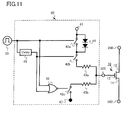
- FIG. 11 is a circuit diagram of the primary components of the semiconductor device according to the present embodiment.
- the semiconductor device according to the present embodiment is, for example, an intelligent power module including an inverter circuit.
- FIG. 11 is a diagram of a switching unit including an inverter circuit.
- FIG. 11 is a circuit diagram of the entire switching unit.
- a gate drive circuit 40 includes a power source terminal 41 to which a power source for gate voltage is connected, switch circuits 42a, 42b, and 42c, resistance elements 43a and 43b, a NOR circuit 45, a voltage suppression diode 44, a delay circuit 46, and a terminal 47 at a potential equal to the potential of the source terminal 100 or a potential lower than the potential of the source terminal 100.
- the voltage suppression diode 44 is, for example, a PIN diode.
- the gate drive circuit 40 is connected to a gate drive signal generation source 30.
- the gate drive circuit 40 controls the gate voltage of the GaN based HEMT 10 in accordance with on and off signals input from the gate drive signal generation source 30.
- the present embodiment can achieve the gate control device, semiconductor device, and method for controlling the semiconductor device that reduce the switching time of a junction field effect transistor. Furthermore, the present embodiment provides a simple circuit configuration because the circuit does not require two power sources for high and low gate voltages.
- the semiconductor device according to the present embodiment is similar to the first embodiment except for that a gate control circuit has a different circuit configuration. Thus, the descriptions of the contents overlapping with the first embodiment will be omitted.
- FIG. 12 is a circuit diagram of the primary components of the semiconductor device according to the present embodiment.
- the semiconductor device according to the present embodiment is, for example, an intelligent power module including an inverter circuit.
- FIG. 12 is a diagram of a switching unit including an inverter circuit.
- FIG. 12 is a circuit diagram of the entire switching unit.
- a gate drive circuit 50 includes a power source terminal 41 to which a power source for gate voltage is connected, switch circuits 42a, 42b, and 42c, resistance elements 43a and 43b, a NOR circuit 45, a voltage suppression diode 54, a delay circuit 46, and a terminal 47 at a potential equal to the potential of the source terminal 100 or a potential lower than the potential of the source terminal 100.
- the voltage suppression diode 54 is a Zener diode.
- the gate drive circuit 50 is connected to the gate drive signal generation source 30.
- the gate drive circuit 50 controls the gate voltage of the GaN based HEMT 10 in accordance with on and off signals input from the gate drive signal generation source 30.
- the present embodiment can achieve the gate control device, semiconductor device, and method for controlling the semiconductor device that reduce the switching time of a junction field effect transistor. Furthermore, the present embodiment provides a simple circuit configuration because the circuit does not require two power sources for high and low gate voltages. Furthermore, using a Zener diode as the voltage suppression diode 54 reduces the temperature dependency that is a characteristic of the gate drive circuit 50.
- the semiconductor device according to the present embodiment is similar to the first embodiment except for that a gate control device is a microcomputer. Thus, the descriptions of the contents overlapping with the first embodiment will be omitted.
- the microcomputer and a control program stored in a memory in the microcomputer control the gate voltage of a junction field effect transistor.
- the present embodiment can achieve the gate control device, semiconductor device, and method for controlling the semiconductor device that reduce the switching time of a junction field effect transistor. Furthermore, using a microcomputer as the gate control device facilitates the control of the gate voltage in synchronization with the operation of the inverter circuit, for example, the time when the inverter circuit gets into a return flow mode.
- the GaN based HEMT has been described as an example of the junction field effect transistor in the embodiments.
- the present disclosure may also be applied to, for example, a transistor made of silicon carbide (SiC) or diamond as long as such a transistor is a junction field effect transistor.
- the intelligent power module including the inverter circuit has been described as an example of the semiconductor device in the embodiments. However, the present disclosure may also be applied to another semiconductor device using a junction field effect transistor.
Landscapes
- Junction Field-Effect Transistors (AREA)
- Power Conversion In General (AREA)
- Electronic Switches (AREA)
Abstract
Description
- This application is based upon and claims the benefit of priority from Japanese Patent Application No.
2014-192014, filed on September 19, 2014 - Embodiments described herein relate generally to a gate control device, a semiconductor device, and a method for controlling the semiconductor device.
- Group III nitride, for example, a gallium nitride (GaN) based semiconductor is expected to be used as a material for next-generation power semiconductor devices. The GaN based semiconductor device has a wider bandgap than that of a silicon (Si) semiconductor device, and thus can achieve a high breakdown voltage and a low loss in comparison to the Si semiconductor device.
- A High Electron Mobility Transistor (HEMT) structure using a two dimensional electron gas (2DEG) as the carrier is widely applied to a GaN based transistor. A junction HEMT is one type of GaN based HEMTs.
- For example, using a p-type GaN based semiconductor for a gate electrode in a junction HEMT can achieve the normally off operation. Meanwhile, injecting a positive hole (hole) from the gate electrode to a channel causes conductivity modulation. This can reduce the on-resistance of the junction HEMT. However, the injection of a hole unfortunately increases the switching time of the junction HEMT.
-
-
FIGS. 1A and 1B are circuit diagrams of the primary components of the semiconductor device according to a first embodiment; -
FIG. 2 is a schematic cross-sectional view of the junction field effect transistor according to the first embodiment; -
FIGS. 3A and 3B are explanatory diagrams of the operation of the junction field effect transistor according to the first embodiment; -
FIGS. 4A and 4B are explanatory diagrams of the threshold voltages of the junction field effect transistor according to the first embodiment; -
FIG. 5 is an explanatory diagram of an exemplary method for controlling the semiconductor device according to the first embodiment; -
FIG. 6 is an explanatory diagram of another exemplary method for controlling the semiconductor device according to the first embodiment; -
FIG. 7 is an explanatory diagram of an exemplary method for controlling the semiconductor device according to a comparative embodiment; -
FIG. 8 is a diagram of the simulation results of the operation of the semiconductor device according to the comparative embodiment; -
FIGS. 9A and 9B are explanatory diagrams of the operation of the junction field effect transistor according to the first embodiment; -
FIG. 10 is an explanatory diagram of an exemplary method for controlling the semiconductor device according to the first embodiment; -
FIG. 11 is a circuit diagram of the primary components of the semiconductor device according to a second embodiment; and -
FIG. 12 is a circuit diagram of the primary components of the semiconductor device according to a third embodiment. - A gate control device of an embodiment is configured to control a gate voltage to be applied to a gate electrode of a junction field effect transistor including a source electrode, a drain electrode, and the gate electrode, the transistor having a first threshold voltage at which the transistor is turned on, and a second threshold voltage at which conductivity modulation occurs in the transistor so as to make the gate voltage equal to or higher than the second threshold voltage when a forward current in a direction from the drain electrode toward the source electrode flows, and so as to make a time variation in the gate voltage have a point from which a rate of the time variation starts decreasing at a voltage between the second threshold voltage and the first threshold voltage when the forward current to be shut down.
- The embodiments of the present disclosure will be described with reference to the appended drawings. Note that, in the description below, the same components and the like are denoted with the same reference signs and the descriptions of the components and the like that have been described are appropriately omitted.
- Herein, the semiconductor device may be a power module that is a combination of a plurality of elements such as a discrete semiconductor. The semiconductor device may be an intelligent power module formed by a plurality of elements such as a discrete semiconductor in which a drive circuit configured to drive the elements or a self-protection function is embedded. The semiconductor device may be an entire system including a power module or an intelligent power module.
- Herein, semiconductors including gallium nitride (GaN), aluminum nitride (AlN), indium nitride (InN), and their intermediate compositions are collectively referred to as a "GaN based semiconductor".
- Herein, a "gate voltage" and a "drain voltage" mean voltages based on a "source voltage".
- A semiconductor device according to the present embodiment includes: a junction field effect transistor including a source electrode, a drain electrode, and a gate electrode, and further including and further including a first threshold voltage at which the transistor is turned on and a current starts flowing between the source electrode and the drain electrode, and a second threshold voltage at which conductivity modulation occurs in the transistor and a current starts flowing between the source electrode and the gate electrode; and a gate control device configured to control a gate voltage to be applied to the gate electrode so as to make the gate voltage equal to or higher than the second threshold voltage when a forward current in a direction from the drain electrode toward the source electrode flows, and so as to make a time variation in the gate voltage have a point from which the rate of the time variation starts decreasing at a voltage between the second threshold voltage and the first threshold voltage when the forward current is shut down.
-
FIGS. 1A and 1B are circuit diagrams of the primary components of the semiconductor device according to the present embodiment. The semiconductor device according to the present embodiment is, for example, an intelligent power module including an inverter circuit.FIGS. 1A and 1B are diagrams of a switching unit included in the inverter circuit.FIG. 1A is a circuit diagram of the entire switching unit, andFIG. 1B is a circuit diagram of an exemplary delay circuit in the switching unit. - The semiconductor device according to the present embodiment includes a GaN based HEMT 10 that is an exemplary junction field effect transistor (JFET), and a
gate drive circuit 20 that is an exemplary gate control device. -
FIG. 2 is a schematic cross-sectional view of the junction field effect transistor according to the present embodiment. The GaN based HEMT 10 is a normally off transistor. The GaN based HEMT 10 includes a GaN channel layer 14, an AlGaN barrier layer 15, asource electrode 11, adrain electrode 12, and agate electrode 13. - The
source electrode 11 and thedrain electrode 12 are, for example, metal. Thegate electrode 13 has, for example, a stacked structure with a p-typeAlGaN capping layer 13a and ametallic layer 13b. -
FIGS. 3A and 3B are explanatory diagrams of the operation of the junction field effect transistor according to the present embodiment. - Two dimensional electron gas (2DEG) is induced on the interface of the GaN channel layer 14 and the AlGaN barrier layer 15 in the GaN based HEMT 10. When a voltage equal to or higher than a first threshold voltage (Vth1) is applied as a gate voltage to the
gate electrode 13, the transistor is turned on. When the transistor is turned on, a current starts flowing between thesource electrode 11 and the drain electrode 12 (FIG. 3A ). - Herein, a current flowing in a direction from the
drain electrode 12 to thesource electrode 11 is referred to as a forward current, and a current flowing in a direction from thesource electrode 11 to thedrain electrode 12 is referred to as a reverse current.FIGS. 3A and 3B illustrates that the forward current flows. Note that the direction of current is opposite to flow direction of electron. - When a gate voltage higher than a forward drop voltage (VF) on the junction of the AlGaN barrier layer 15 and the p-type
AlGaN capping layer 13a is applied to thegate electrode 13, a hole is injected from thegate electrode 13 to the channel layer 14. This causes the conductivity modulation (FIG. 3B ). The gate voltage at which the conductivity modulation occurs is a second threshold voltage (Vth2). The conductivity modulation reduces the on-resistance of the GaN basedHEMT 10. Meanwhile, the gate current flows between thegate electrode 13 and thesource electrode 11. -
FIGS. 4A and 4B are explanatory diagrams of the threshold voltages of the junction field effect transistor according to the present embodiment.FIG. 4A is a diagram of the definition of the first threshold voltage (Vth1) andFIG. 4B is a diagram of the definition of the second threshold voltage (Vth2). - As illustrated in
FIG. 4A , the first threshold voltage (Vth1) at which the transistor is turned on is defined as the value of the x-axis intercept when the tangent to the curve of current and voltage has the largest gradient while the gate voltage is shown on the X axis and the drain current is shown on the Y axis. As illustrated inFIG. 4B , the second threshold voltage (Vth2) at which the conductivity modulation occurs in the transistor is defined as the value of the x-axis intercept when the tangent to the curve of current and voltage has the largest gradient while the gate voltage is shown on the X axis and the gate current is shown on the Y axis. The voltage and current are measured while the drain voltage (Vd) = 1 V holds. - As illustrated in
FIG. 1A , thesource electrode 11, thedrain electrode 12, and thegate electrode 13 are connected to thesource terminal 100, thedrain terminal 200, and thegate terminal 300, respectively, in the GaN basedHEMT 10. Thedrain terminal 200 is connected, for example, to an inductive load such as a motor. - The
gate drive circuit 20 includes: a power source terminal 21a to which a power source for high gate voltage (VgH) is connected; a power source terminal 21b to which a power source for low gate voltage (VgL) is connected;switch circuits resistance elements XOR circuit 24; a NORcircuit 25; adelay circuit 26; and a terminal 27 at a potential equal to the potential of thesource terminal 100 or a potential lower than the potential of thesource terminal 100.FIG. 1B illustrates an example of thedelay circuit 26. - The
gate drive circuit 20 is connected to a gate drivesignal generation source 30. Thegate drive circuit 20 controls the gate voltage of the GaN basedHEMT 10 in accordance with on and off signals input from the gate drivesignal generation source 30. - The
gate drive circuit 20 has a function of controlling the gate voltage so as to make the gate voltage equal to or higher than the second threshold voltage (Vth2) when the forward current in the direction from thedrain electrode 12 toward thesource electrode 11 flows, and controlling the gate voltage so as to make the time variation in gate voltage have a point from which the rate of the time variation starts decreasing at a voltage between the second threshold voltage (Vth2) and the first threshold voltage (Vth1) when the forward current to be shut down. - Next, a method for controlling the semiconductor device according to the present embodiment will be described.
- The method for controlling the semiconductor device according to the present embodiment is used to control the gate voltage so as to make the gate voltage equal to or higher than the second threshold voltage when the forward current flows from the drain electrode toward the source electrode. The gate voltage is applied to the gate electrode of the junction field effect transistor including the source electrode, the drain electrode, and the gate electrode, and having the first threshold voltage at which a current starts flowing between the source electrode and the drain electrode, and the second threshold voltage at which a current starts flowing between the source electrode and the gate electrode. The method is used to control the gate voltage so as to make the time variation in gate voltage have a point from which the rate of the time variation starts decreasing at a voltage between the second threshold voltage and the first threshold voltage when the forward current to be shut down.
-
FIG. 5 is an explanatory diagram of an exemplary method for controlling the semiconductor device according to the present embodiment. The time is shown on the horizontal axis, and the gate voltage (Vgs) applied to thegate electrode 13 of the GaN basedHEMT 10 illustrated inFIG. 1A is shown on the vertical axis. - When the GaN based
HEMT 10 is turned on, in other words, when the forward current in the direction from thedrain electrode 12 toward thesource electrode 11 flows, thegate drive circuit 20 controls the gate voltage so as to make the gate voltage equal to or higher than the second threshold voltage (Vth2). The gate voltage equal to or higher than the second threshold voltage (Vth2) injects a hole to the channel layer 14, and thus causes the conductivity modulation. This maintains a low on-resistance of the GaN basedHEMT 10. - Next, when the GaN based
HEMT 10 is turned off, in other words, when the forward current is shut down, thegate drive circuit 20 controls the gate voltage so as to make the time variation in gate voltage have a point from which the rate of the time variation starts decreasing at a voltage between the second threshold voltage (Vth2) and the first threshold voltage ((Vth1) (a point P inFIG. 5 ). Subsequently, thegate drive circuit 20 controls the gate voltage so as to make the gate voltage lower than the first threshold voltage (Vth1). -
FIG. 5 illustrates that thegate drive circuit 20 controls the gate voltage so as to vary the gate voltage in a staircase pattern and maintain the gate voltage at a constant voltage between the second threshold voltage (Vth2) and the first threshold voltage (Vth1) for a predetermined time (td). In the case ofFIG. 5 , the rate of time variation in gate voltage becomes zero at the point P. - In the
gate drive circuit 20 illustrated inFIG. 1A , a voltage (VgH) equal to or higher than the second threshold voltage (Vth2) is supplied from thepower source terminal 21a, and a voltage (VgL)between the second threshold voltage (Vth2) and the first threshold voltage (Vth1) is supplied from thepower source terminal 21b. -
FIG. 6 is an explanatory diagram of another exemplary method for controlling the semiconductor device according to the present embodiment. The time is shown on the horizontal axis, and the gate voltage applied to thegate electrode 13 of the GaN basedHEMT 10 illustrated inFIG. 1A is shown on the vertical axis. - Differently from
FIG. 5 , the gate voltage is gradually reduced when the GaN basedHEMT 10 is turned off inFIG. 6 . Also inFIG. 6 , the gate voltage is controlled such that the time variation in gate voltage has a point from which the rate of the time variation starts decreasing at a voltage between the second threshold voltage (Vth2) and the first threshold voltage ((Vth1) (a point P inFIG. 6 ). In the case ofFIG. 6 , the gate voltage is maintained at a voltage between the second threshold voltage (Vth2) and the first threshold voltage (Vth1) for a predetermined time (td). In the case ofFIG. 6 , the gate voltage is controlled such that a curve of time and voltage has an inflection point protruding downward between the second threshold voltage (Vth2) and the first threshold voltage (Vth1). - Next, the functions and effects of the present embodiment will be described.
-
FIG. 7 is an explanatory diagram of an exemplary method for controlling the semiconductor device according to a comparative embodiment. The time is shown on the horizontal axis, and a gate voltage (Vgs) to be applied to a gate electrode of a GaN based HEMT is shown on the vertical axis. - Similarly to the present embodiment, the gate voltage is controlled such that the gate voltage is equal to or higher than a second threshold voltage (Vth2) in the comparative embodiment when the GaN based HEMT is turned on. On the other hand, differently from the present embodiment, the gate voltage is linearly reduced to zero when the GaN based HEMT is turned off.
- In the comparative embodiment, the hole injected into the channel layer remains after the gate voltage decreases to zero. The drain current continues flowing until the hole disappears. This unfortunately elongates the switching time.
- According to the present embodiment, when the GaN based
HEMT 10 is turned off, in other words, when the forward current is shut down, thegate drive circuit 20 controls the gate voltage so as to make the time variation in gate voltage have a point from which the rate of the time variation starts decreasing at a voltage between the second threshold voltage (Vth2) and the first threshold voltage ((Vth1) (the points P inFIGS. 5 and6 ). This control maintains the state in which the transistor is on without the injection of a hole for a predetermined time (td) until the time when the gate voltage becomes zero. - Providing a period of time in which a hole is not injected causes the hole in the channel layer 14 to disappear in the period. This can reduce the switching time of the GaN based
HEMT 10. -
FIG. 8 illustrates the waveforms of the actual measurement of the operation of the semiconductor device according to the comparative embodiment. To measure the delay of the switching time due to the hole, the gate voltage is reduced to a negative voltage. - It takes 18 nanoseconds for the drain voltage to reach a desired value even when the HEMT is turned off after the gate voltage sufficiently decreases. The hole can remain in the channel layer at least for the period of 18 nanoseconds.
- Thus, the predetermined time (td) in which the gate voltage is maintained at a voltage between the second threshold voltage (Vth2) and the first threshold voltage (Vth1) is preferably equal to or longer than 18 nanoseconds in the present embodiment.
- Next, the case in which the semiconductor device according to the present embodiment is controlled in the following manner in the method for controlling the semiconductor device according to the present embodiment will be described. When the reverse current in the direction from the source electrode toward the drain electrode flows, the semiconductor device is controlled such that the difference between the gate voltage and the drain voltage is equal to or higher than the second threshold voltage. When the difference between the gate voltage and the drain voltage is reduced from the second threshold voltage, the semiconductor device is controlled such that the time variation in difference between the gate voltage and the drain voltage has a point from which the rate of the time variation starts decreasing at a voltage between the second threshold voltage and the first threshold voltage and the difference between the gate voltage and the drain voltage is subsequently kept equal to or lower than the first threshold voltage.
- The case in which the reverse current in the direction from the source electrode toward the drain electrode flows is, for example, the case in which the semiconductor device is a switching unit including an inverter circuit and a return current flows in the GaN based
HEMT 10. In other words, the case in which a relatively positive voltage is applied to thesource terminal 100 and a relatively negative voltage is applied to thedrain terminal 200 inFIGS. 1A and 1B . -
FIGS. 9A and 9B are explanatory diagrams of the operation of the junction field effect transistor according to the first embodiment. The operation for causing the reverse current in the direction from thesource electrode 11 toward thedrain electrode 12 to flow will be described. When the reverse current flows, the voltage of thesource electrode 11 is relatively higher than that of thedrain electrode 12. - Two dimensional electron gas (2DEG) is induced on the interface between the GaN channel layer 14 and the AlGaN barrier layer 15 in the GaN based
HEMT 10. When a voltage at which the difference between the gate voltage and the drain voltage is equal to or higher than the first threshold voltage (Vth1) is applied to thegate electrode 13 and thedrain electrode 12, the transistor is turned on. When the transistor is turned on, a current starts flowing between thesource electrode 11 and the drain electrode 12 (FIG. 9A ). - As described above, the current in the direction from the
drain electrode 12 toward thesource electrode 11 is referred to as the forward current, and the current in the direction from thesource electrode 11 toward thedrain electrode 12 is referred to as the reverse current herein.FIGS. 9A and 9B illustrates that the reverse current flows. - When a voltage at which the difference between the gate voltage and the drain voltage is equal to or higher than the second threshold voltage (Vth2) is applied to the
gate electrode 13 and thedrain electrode 12, the conductivity modulation occurs. This reduces the on-resistance of the GaN based HEMT 10 (FIG. 9B ). - The
gate drive circuit 20 preferably includes a function of controlling the gate voltage in the following manner. When the reverse current in the direction from thesource electrode 11 toward thedrain electrode 12 flows, thegate drive circuit 20 controls the difference between the gate voltage and the drain voltage so as to make the difference between the gate voltage and the drain voltage equal to or higher than the second threshold voltage (Vth2). When the difference between the gate voltage and the drain voltage is reduced from the second threshold voltage (Vth2), thegate drive circuit 20 controls the difference between the gate voltage and the drain voltage so as to make the time variation in difference between the gate voltage and the drain voltage have a point from which the rate of the time variation starts decreasing at a voltage between the second threshold voltage (Vth2) and the first threshold voltage (Vth1), and so as to subsequently keep the difference between the gate voltage and the drain voltage equal to or lower than the first threshold voltage (Vth1). - The semiconductor device is preferably controlled in the following manner in the method for controlling the semiconductor device according to the first embodiment. When the reverse current in the direction from the
source electrode 11 toward thedrain electrode 12 flows, the semiconductor device is controlled such that the difference between the gate voltage and the drain voltage is equal to or higher than the second threshold voltage (Vth2). When the difference between the gate voltage and the drain voltage is reduced from the second threshold voltage (Vth2), the semiconductor device is controlled such that the time variation in difference between the gate voltage and the drain voltage has a point from which the rate of the time variation starts decreasing at a voltage between the second threshold voltage (Vth2) and the first threshold voltage (Vth1), and the difference between the gate voltage and the drain voltage is kept equal to or lower than the first threshold voltage (Vth1). -
FIG. 10 is an explanatory diagram of an exemplary method for controlling the semiconductor device according to the present embodiment. The upper graph illustrates the time on the horizontal axis and the difference between the gate voltage and the drain voltage (Vgs - Vds) applied to thegate electrode 13 and thedrain electrode 12 of the GaN basedHEMT 10 illustrated inFIG. 1 on the vertical axis. The lower graph illustrates the reverse current flowing in the GaN basedHEMT 10. - As illustrated in the lower graph, a return current flows in the GaN based
HEMT 10 during a return flow period. In other words, the reverse current flows. The operation of the inverter circuit determines the return flow period. - Generally, the on-resistance of the GaN based
HEMT 10 is reduced and thus the loss is reduced for a predetermined period of time in the return flow period. Thus, the difference between the gate voltage and the drain voltage is raised to a predetermined voltage. The period is referred to as a synchronous rectification period. If the return flow period is in agreement with the synchronous rectification period, a short circuit may unfortunately occur in the inverter circuit. Thus, a time lag is generally provided between the return flow period and the synchronous rectification period. A time lag before the completion of the return flow period is referred to as a second predetermined time (tdr2). - If the difference between the gate voltage and the drain voltage is linearly reduced to zero when the synchronous rectification period is terminated, the hole remains in the channel layer even after the difference between the gate voltage and the drain voltage becomes zero. Thus, if the second predetermined time (tdr2) is short, the reverse recovery current flows in the GaN based
HEMT 10 even after the completion of the return flow period. This may unfortunately cause a short circuit in the inverter circuit. - According to the present embodiment, when the difference between the gate voltage and the drain voltage is reduced from the second threshold voltage (Vth2) in the synchronous rectification period, the difference between the gate voltage and the drain voltage is controlled such that the time variation in difference between the gate voltage and the drain voltage has a point at which the rate of the time variation starts decreasing at a voltage between the second threshold voltage (Vth2) and the first threshold voltage ((Vth1) (a point P in the upper graph in
FIG. 10 ), and the difference between the gate voltage and the drain voltage is subsequently kept equal to or lower than the first threshold voltage (Vth1). - This maintains the state in which the transistor is on without the injection of a hole for the predetermined time (tdr1) in the synchronous rectification period.
- Providing a period of time in which a hole is not injected causes the hole in the channel layer 14 to disappear in the period. This can prevent the reverse recovery current from flowing in the GaN based
HEMT 10 and thus can prevent a short circuit from occurring in the inverter circuit. - In particular, the difference between the gate voltage and the drain voltage is controlled in the following manner in the example of
FIG. 10 . When the difference between the gate voltage and the drain voltage is reduced from the second threshold voltage (Vth2) while varying in a staircase pattern, the difference between the gate voltage and the drain voltage is controlled such that the difference is maintained at a constant voltage between the second threshold voltage (Vth2) and the first threshold voltage for the first predetermined time (tdr1). Subsequently, the difference between the gate voltage and the drain voltage is kept lower than the first threshold voltage ((Vth1) for the second predetermined time (tdr2) by the time when the reverse current is shut down, in other words, by the completion of the return flow period. In the case ofFIG. 10 , the rate of time variation in difference between the gate voltage and the drain voltage becomes zero at the point P. - The sum of the first predetermined time (tdr1) and the second predetermined time (tdr2) is preferably equal to or longer than 18 nanoseconds in terms of preventing the reverse recovery current from flowing in the GaN based
HEMT 10 after the completion of the return flow period. - As described above, the present embodiment can achieve the gate control device, semiconductor device, and method for controlling the semiconductor device that reduce the switching time of a junction field effect transistor.
- The semiconductor device according to the present embodiment is similar to the first embodiment except for that a gate control circuit has a different circuit configuration. Thus, the descriptions of the contents overlapping with the first embodiment will be omitted.
-
FIG. 11 is a circuit diagram of the primary components of the semiconductor device according to the present embodiment. The semiconductor device according to the present embodiment is, for example, an intelligent power module including an inverter circuit.FIG. 11 is a diagram of a switching unit including an inverter circuit.FIG. 11 is a circuit diagram of the entire switching unit. - A
gate drive circuit 40 according to the present embodiment includes apower source terminal 41 to which a power source for gate voltage is connected,switch circuits resistance elements circuit 45, a voltage suppression diode 44, adelay circuit 46, and a terminal 47 at a potential equal to the potential of thesource terminal 100 or a potential lower than the potential of thesource terminal 100. The voltage suppression diode 44 is, for example, a PIN diode. - The
gate drive circuit 40 is connected to a gate drivesignal generation source 30. Thegate drive circuit 40 controls the gate voltage of the GaN basedHEMT 10 in accordance with on and off signals input from the gate drivesignal generation source 30. - Similarly to the first embodiment, the present embodiment can achieve the gate control device, semiconductor device, and method for controlling the semiconductor device that reduce the switching time of a junction field effect transistor. Furthermore, the present embodiment provides a simple circuit configuration because the circuit does not require two power sources for high and low gate voltages.
- The semiconductor device according to the present embodiment is similar to the first embodiment except for that a gate control circuit has a different circuit configuration. Thus, the descriptions of the contents overlapping with the first embodiment will be omitted.
-
FIG. 12 is a circuit diagram of the primary components of the semiconductor device according to the present embodiment. The semiconductor device according to the present embodiment is, for example, an intelligent power module including an inverter circuit.FIG. 12 is a diagram of a switching unit including an inverter circuit.FIG. 12 is a circuit diagram of the entire switching unit. - A
gate drive circuit 50 according to the present embodiment includes apower source terminal 41 to which a power source for gate voltage is connected,switch circuits resistance elements circuit 45, avoltage suppression diode 54, adelay circuit 46, and a terminal 47 at a potential equal to the potential of thesource terminal 100 or a potential lower than the potential of thesource terminal 100. Thevoltage suppression diode 54 is a Zener diode. - The
gate drive circuit 50 is connected to the gate drivesignal generation source 30. Thegate drive circuit 50 controls the gate voltage of the GaN basedHEMT 10 in accordance with on and off signals input from the gate drivesignal generation source 30. - Similarly to the first embodiment, the present embodiment can achieve the gate control device, semiconductor device, and method for controlling the semiconductor device that reduce the switching time of a junction field effect transistor. Furthermore, the present embodiment provides a simple circuit configuration because the circuit does not require two power sources for high and low gate voltages. Furthermore, using a Zener diode as the
voltage suppression diode 54 reduces the temperature dependency that is a characteristic of thegate drive circuit 50. - The semiconductor device according to the present embodiment is similar to the first embodiment except for that a gate control device is a microcomputer. Thus, the descriptions of the contents overlapping with the first embodiment will be omitted.
- According to the present embodiment, for example, the microcomputer and a control program stored in a memory in the microcomputer control the gate voltage of a junction field effect transistor.
- Similarly to the first embodiment, the present embodiment can achieve the gate control device, semiconductor device, and method for controlling the semiconductor device that reduce the switching time of a junction field effect transistor. Furthermore, using a microcomputer as the gate control device facilitates the control of the gate voltage in synchronization with the operation of the inverter circuit, for example, the time when the inverter circuit gets into a return flow mode.
- The examples in which the combination of a logic circuit and an analog circuit, and a microcomputer are used as the gate control device have been described in the embodiments. However, for example, an integrated circuit (IC) dedicated for gate control may be used as long as the gate control according to the present disclosure can be achieved.
- The GaN based HEMT has been described as an example of the junction field effect transistor in the embodiments. However, the present disclosure may also be applied to, for example, a transistor made of silicon carbide (SiC) or diamond as long as such a transistor is a junction field effect transistor.
- The intelligent power module including the inverter circuit has been described as an example of the semiconductor device in the embodiments. However, the present disclosure may also be applied to another semiconductor device using a junction field effect transistor.
- While certain embodiments have been described, these embodiments have been presented by way of example only, and are not intended to limit the scope of the inventions. Indeed, the gate control device, the semiconductor device and method for controlling the semiconductor device described herein may be embodied in a variety of other forms; furthermore, various omissions, substitutions and changes in the form of the devices and methods described herein may be made without departing from the spirit of the inventions. The accompanying claims and their equivalents are intended to cover such forms or modifications as would fall within the scope and spirit of the inventions.
Claims (15)
- A gate control device configured to control a gate voltage to be applied to a gate electrode of a junction field effect transistor including a source electrode, a drain electrode, and the gate electrode, the transistor having a first threshold voltage at which the transistor is turned on, and a second threshold voltage at which conductivity modulation occurs in the transistor
so as to make the gate voltage equal to or higher than the second threshold voltage when a forward current in a direction from the drain electrode toward the source electrode flows, and
so as to make a time variation in the gate voltage have a point from which a rate of the time variation starts decreasing at a voltage between the second threshold voltage and the first threshold voltage when the forward current to be shut down. - The device according to claim 1, configured to further control the gate voltage so as to maintain the gate voltage at a voltage between the second threshold voltage and the first threshold voltage for a predetermined time when the forward current to be shut down.
- The device according to claim 2, wherein the predetermined time is equal to or longer than 18 nanoseconds.
- The device according to claim 1, configured to further control a difference between the gate voltage and a drain voltage so as to make the difference equal to or higher than the second threshold voltage when a reverse current in a direction from the source electrode toward the drain electrode flows, and
so as to make a time variation in the difference between the gate voltage and the drain voltage have a point from which a rate of the time variation starts decreasing at a voltage between the second threshold voltage and the first threshold voltage and so as to subsequently keep the difference lower than the first threshold voltage when the difference is reduced from the second threshold voltage. - The device according to claim 4, configured to further control the difference between the gate voltage and the drain voltage so as to maintain the difference at a voltage between the second threshold voltage and the first threshold voltage for a first predetermined time and subsequently keep the difference less than the first threshold voltage for a second predetermined time by a time when the reverse current is shut down when the difference is reduced from the second threshold voltage.
- The device according to claim 5, wherein a sum of the first predetermined time and the second predetermined time is equal to or longer than 18 nanoseconds.
- A semiconductor device comprising:a junction field effect transistor including a source electrode, a drain electrode, and a gate electrode, the transistor having a first threshold voltage at which the transistor is turned on, and a second threshold voltage at which conductivity modulation occurs in the transistor; anda gate control device according to any preceding claim.
- The device according to claim 7, wherein the junction field effect transistor is a GaN based HEMT.
- A method for controlling a semiconductor device, the method comprising:controlling a gate voltage to be applied to a gate electrode of a junction field effect transistor including a source electrode, a drain electrode, and the gate electrode, the transistor having a first threshold voltage at which the transistor is turned on, and a second threshold voltage at which conductivity modulation occurs in the transistorso as to make the gate voltage equal to or higher than the second threshold voltage when a forward current in a direction from the drain electrode toward the source electrode flows, andso as to make a time variation in the gate voltage have a point from which a rate of the time variation starts decreasing at a voltage between the second threshold voltage and the first threshold voltage when the forward current to be shut down.
- The method according to claim 9, further comprising:controlling the gate voltage so as to maintain the gate voltage at a voltage between the second threshold voltage and the first threshold voltage for a predetermined time when the forward current to be shut down.
- The method according to claim 10, wherein the predetermined time is equal to or longer than 18 nanoseconds.
- The method according to claim 9, further comprising:controlling a difference between the gate voltage and a drain voltage so as to make the difference equal to or higher than the second threshold voltage when a reverse current in a direction from the source electrode toward the drain electrode flows, andso as to make a time variation in the difference between the gate voltage and the drain voltage have a point from which a rate of the time variation starts decreasing at a voltage between the second threshold voltage and the first threshold voltage and so as to subsequently keep the difference lower than the first threshold voltage when the difference is reduced from the second threshold voltage.
- The method according to claim 12, further comprising:controlling the difference between the gate voltage and the drain voltage so as to maintain the difference at a voltage between the second threshold voltage and the first threshold voltage for a first predetermined time and subsequently keep the difference less than the first threshold voltage for a second predetermined time by a time when the reverse current is shut down when the difference is reduced from the second threshold voltage.
- The method according to claim 13, wherein a sum of the first predetermined time and the second predetermined time is equal to or longer than 18 nanoseconds.
- A gate control device for controlling a gate voltage to be applied to a gate electrode of a junction field effect transistor including a source electrode, a drain electrode, and the gate electrode, the transistor having a first threshold voltage at which the transistor is turned on, and a second threshold voltage at which conductivity modulation occurs in the transistor
so as to make the gate voltage equal to or higher than the second threshold voltage when a forward current in a direction from the drain electrode toward the source electrode flows, and
so as to make a time variation in the gate voltage have a point from which a rate of the time variation starts decreasing at a voltage between the second threshold voltage and the first threshold voltage when the forward current to be shut down.
Applications Claiming Priority (1)
| Application Number | Priority Date | Filing Date | Title |
|---|---|---|---|
| JP2014192014A JP6223938B2 (en) | 2014-09-19 | 2014-09-19 | Gate control device, semiconductor device, and control method of semiconductor device |
Publications (2)
| Publication Number | Publication Date |
|---|---|
| EP2999118A1 true EP2999118A1 (en) | 2016-03-23 |
| EP2999118B1 EP2999118B1 (en) | 2019-06-12 |
Family
ID=53773338
Family Applications (1)
| Application Number | Title | Priority Date | Filing Date |
|---|---|---|---|
| EP15179431.0A Active EP2999118B1 (en) | 2014-09-19 | 2015-07-31 | Gate control device, semiconductor device, and method for controlling semiconductor device |
Country Status (3)
| Country | Link |
|---|---|
| US (1) | US9621153B2 (en) |
| EP (1) | EP2999118B1 (en) |
| JP (1) | JP6223938B2 (en) |
Cited By (3)
| Publication number | Priority date | Publication date | Assignee | Title |
|---|---|---|---|---|
| CN109217645A (en) * | 2018-11-01 | 2019-01-15 | 南京航空航天大学 | A kind of nonisulated grid-type GaN HEMT driving circuit and control method |
| CN112640124A (en) * | 2018-06-27 | 2021-04-09 | 李湛明 | Gallium nitride device, gate drive circuit of integrated circuit and voltage regulator |
| WO2021176003A1 (en) * | 2020-03-05 | 2021-09-10 | Robert Bosch Gmbh | Driver circuit for a low inductive power module and a low inductive power module with enhanced short circuit withstand capability |
Families Citing this family (16)
| Publication number | Priority date | Publication date | Assignee | Title |
|---|---|---|---|---|
| JP6023825B2 (en) * | 2015-01-14 | 2016-11-09 | 株式会社豊田中央研究所 | Semiconductor device |
| JP2016220421A (en) * | 2015-05-21 | 2016-12-22 | トヨタ自動車株式会社 | Non-contact power transmission device and power transmission system |
| US10892356B2 (en) | 2016-06-24 | 2021-01-12 | Cree, Inc. | Group III-nitride high-electron mobility transistors with buried p-type layers and process for making the same |
| US12484244B2 (en) | 2016-06-24 | 2025-11-25 | Wolfspeed, Inc. | Group III-nitride high-electron mobility transistors with gate connected buried p-type layers and process for making the same |
| US11430882B2 (en) | 2016-06-24 | 2022-08-30 | Wolfspeed, Inc. | Gallium nitride high-electron mobility transistors with p-type layers and process for making the same |
| US10741682B2 (en) | 2016-11-17 | 2020-08-11 | Semiconductor Components Industries, Llc | High-electron-mobility transistor (HEMT) semiconductor devices with reduced dynamic resistance |
| US10158355B2 (en) * | 2016-12-20 | 2018-12-18 | Raytheon Company | System and method for inrush current control for power sources using non-linear algorithm |
| JP2018196026A (en) * | 2017-05-18 | 2018-12-06 | 株式会社豊田中央研究所 | Gate driving device |
| US11133740B2 (en) | 2019-12-18 | 2021-09-28 | Cypress Semiconductor Corporation | Startup regulator using voltage buffer to stabilize power supply voltage |
| CN111786560B (en) * | 2020-06-23 | 2025-06-13 | 杰华特微电子股份有限公司 | A synchronous rectification control method, control circuit and switching power supply |
| US12557322B2 (en) | 2021-05-17 | 2026-02-17 | Wolfspeed, Inc. | Group III-nitride transistors with back barrier structures and buried p-type layers and methods thereof |
| US11929428B2 (en) | 2021-05-17 | 2024-03-12 | Wolfspeed, Inc. | Circuits and group III-nitride high-electron mobility transistors with buried p-type layers improving overload recovery and process for implementing the same |
| US12402346B2 (en) * | 2021-05-17 | 2025-08-26 | Wolfspeed, Inc. | Circuits and group III-nitride transistors with buried p-layers and controlled gate voltages and methods thereof |
| TWI852168B (en) * | 2022-11-16 | 2024-08-11 | 立積電子股份有限公司 | Swtch device |
| TWI865988B (en) | 2022-12-14 | 2024-12-11 | 立積電子股份有限公司 | Switch device |
| CN117133805A (en) * | 2023-10-16 | 2023-11-28 | 重庆邮电大学 | Mixed drain electrode enhanced GaN high electron mobility transistor |
Citations (5)
| Publication number | Priority date | Publication date | Assignee | Title |
|---|---|---|---|---|
| EP0817381A2 (en) * | 1996-07-05 | 1998-01-07 | Mitsubishi Denki Kabushiki Kaisha | Semiconductor device drive circuit |
| US20090066402A1 (en) * | 2007-09-12 | 2009-03-12 | Mitsubishi Electric Corporation | Gate drive circuit |
| US20110133790A1 (en) * | 2009-12-07 | 2011-06-09 | Denso Corporation | Device for driving switching elements |
| EP2418774A1 (en) * | 2010-08-09 | 2012-02-15 | Honda Motor Co., Ltd. | Semiconductor device driving unit and method |
| US20120153998A1 (en) * | 2009-09-15 | 2012-06-21 | Mitsubishi Electric Corporation | Gate drive circuit |
Family Cites Families (6)
| Publication number | Priority date | Publication date | Assignee | Title |
|---|---|---|---|---|
| JP4712459B2 (en) | 2005-07-08 | 2011-06-29 | パナソニック株式会社 | Transistor and method of operating the same |
| JP5061998B2 (en) * | 2008-03-28 | 2012-10-31 | 株式会社デンソー | Switching circuit |
| JP2013042193A (en) * | 2009-12-03 | 2013-02-28 | Panasonic Corp | Switch device |
| JP5556726B2 (en) * | 2011-04-04 | 2014-07-23 | サンケン電気株式会社 | Switching circuit |
| JP5681567B2 (en) | 2011-05-24 | 2015-03-11 | パナソニックIpマネジメント株式会社 | Switch device |
| JP5545308B2 (en) * | 2012-02-28 | 2014-07-09 | 株式会社豊田中央研究所 | Driving circuit |
-
2014
- 2014-09-19 JP JP2014192014A patent/JP6223938B2/en active Active
-
2015
- 2015-07-31 EP EP15179431.0A patent/EP2999118B1/en active Active
- 2015-08-12 US US14/824,228 patent/US9621153B2/en active Active
Patent Citations (5)
| Publication number | Priority date | Publication date | Assignee | Title |
|---|---|---|---|---|
| EP0817381A2 (en) * | 1996-07-05 | 1998-01-07 | Mitsubishi Denki Kabushiki Kaisha | Semiconductor device drive circuit |
| US20090066402A1 (en) * | 2007-09-12 | 2009-03-12 | Mitsubishi Electric Corporation | Gate drive circuit |
| US20120153998A1 (en) * | 2009-09-15 | 2012-06-21 | Mitsubishi Electric Corporation | Gate drive circuit |
| US20110133790A1 (en) * | 2009-12-07 | 2011-06-09 | Denso Corporation | Device for driving switching elements |
| EP2418774A1 (en) * | 2010-08-09 | 2012-02-15 | Honda Motor Co., Ltd. | Semiconductor device driving unit and method |
Non-Patent Citations (1)
| Title |
|---|
| YASUHIRO UEMOTO; TETSUZO UEDA; TSUYOSHI TANAKA; DAISUKE UEDA: "Recent advances of high voltage AlGaN/GaN power HFETs", SPIE GALLIUM NITRIDE MATERIALS AND DEVICES IV, vol. 7216, 17 February 2009 (2009-02-17), XP040493166 * |
Cited By (5)
| Publication number | Priority date | Publication date | Assignee | Title |
|---|---|---|---|---|
| CN112640124A (en) * | 2018-06-27 | 2021-04-09 | 李湛明 | Gallium nitride device, gate drive circuit of integrated circuit and voltage regulator |
| CN112640124B (en) * | 2018-06-27 | 2024-02-20 | 苏州量芯微半导体有限公司 | Gate driving circuit of gallium nitride device and integrated circuit and voltage regulator |
| CN109217645A (en) * | 2018-11-01 | 2019-01-15 | 南京航空航天大学 | A kind of nonisulated grid-type GaN HEMT driving circuit and control method |
| WO2021176003A1 (en) * | 2020-03-05 | 2021-09-10 | Robert Bosch Gmbh | Driver circuit for a low inductive power module and a low inductive power module with enhanced short circuit withstand capability |
| US11962291B2 (en) | 2020-03-05 | 2024-04-16 | Robert Bosch Gmbh | Driver circuit for a low inductive power module and a low inductive power module with enhanced short circuit withstand capability |
Also Published As
| Publication number | Publication date |
|---|---|
| US20160087625A1 (en) | 2016-03-24 |
| US9621153B2 (en) | 2017-04-11 |
| EP2999118B1 (en) | 2019-06-12 |
| JP2016063498A (en) | 2016-04-25 |
| JP6223938B2 (en) | 2017-11-01 |
Similar Documents
| Publication | Publication Date | Title |
|---|---|---|
| EP2999118B1 (en) | Gate control device, semiconductor device, and method for controlling semiconductor device | |
| JP5811800B2 (en) | Control circuit and electronic equipment | |
| CN105939151B (en) | Electronic circuit | |
| US9793824B2 (en) | Gate driving circuit, semiconductor device, and power conversion device | |
| US9236373B2 (en) | Semiconductor device | |
| US20120241756A1 (en) | High Voltage Composite Semiconductor Device with Protection for a Low Voltage Device | |
| EP3324544A1 (en) | Semiconductor device | |
| EP2966779A1 (en) | Semiconductor device | |
| KR102112299B1 (en) | Driving method and driving circuit for power switching device | |
| TW201509129A (en) | Gate driver for a semiconductor device based circuit | |
| CN111758210B (en) | Rectifier circuit and power supply device | |
| US9059697B2 (en) | Drive circuit and drive method for driving normally-on-type transistor | |
| US20150349632A1 (en) | Controlling a pair of switches | |
| Nishigaki et al. | An analysis of false turn-on mechanism on power devices | |
| US9972992B2 (en) | Protection circuit of semiconductor device | |
| US9912332B2 (en) | Semiconductor device | |
| US20160248422A1 (en) | Switching circuit, semiconductor switching arrangement and method | |
| Saito et al. | Relation between UIS withstanding capability and IV characteristics in high-voltage GaN-HEMTs | |
| US9762232B2 (en) | Semiconductor device | |
| CN104620484A (en) | Devices and components for power conversion circuits | |
| US11264899B2 (en) | Semiconductor device | |
| US9461637B2 (en) | Method and apparatus for controlling a gate voltage in high electron mobility transistor | |
| US20160218099A1 (en) | Semiconductor device | |
| US20140167721A1 (en) | Power supply device | |
| US9673312B2 (en) | Power semiconductor device with over-current protection |
Legal Events
| Date | Code | Title | Description |
|---|---|---|---|
| PUAI | Public reference made under article 153(3) epc to a published international application that has entered the european phase |
Free format text: ORIGINAL CODE: 0009012 |
|
| 17P | Request for examination filed |
Effective date: 20150731 |
|
| AK | Designated contracting states |
Kind code of ref document: A1 Designated state(s): AL AT BE BG CH CY CZ DE DK EE ES FI FR GB GR HR HU IE IS IT LI LT LU LV MC MK MT NL NO PL PT RO RS SE SI SK SM TR |
|
| AX | Request for extension of the european patent |
Extension state: BA ME |
|
| STAA | Information on the status of an ep patent application or granted ep patent |
Free format text: STATUS: EXAMINATION IS IN PROGRESS |
|
| 17Q | First examination report despatched |
Effective date: 20170908 |
|
| GRAP | Despatch of communication of intention to grant a patent |
Free format text: ORIGINAL CODE: EPIDOSNIGR1 |
|
| STAA | Information on the status of an ep patent application or granted ep patent |
Free format text: STATUS: GRANT OF PATENT IS INTENDED |
|
| INTG | Intention to grant announced |
Effective date: 20181221 |
|
| GRAS | Grant fee paid |
Free format text: ORIGINAL CODE: EPIDOSNIGR3 |
|
| GRAA | (expected) grant |
Free format text: ORIGINAL CODE: 0009210 |
|
| STAA | Information on the status of an ep patent application or granted ep patent |
Free format text: STATUS: THE PATENT HAS BEEN GRANTED |
|
| AK | Designated contracting states |
Kind code of ref document: B1 Designated state(s): AL AT BE BG CH CY CZ DE DK EE ES FI FR GB GR HR HU IE IS IT LI LT LU LV MC MK MT NL NO PL PT RO RS SE SI SK SM TR |
|
| REG | Reference to a national code |
Ref country code: GB Ref legal event code: FG4D |
|
| REG | Reference to a national code |
Ref country code: CH Ref legal event code: EP |
|
| REG | Reference to a national code |
Ref country code: AT Ref legal event code: REF Ref document number: 1143908 Country of ref document: AT Kind code of ref document: T Effective date: 20190615 |
|
| REG | Reference to a national code |
Ref country code: DE Ref legal event code: R096 Ref document number: 602015031677 Country of ref document: DE |
|
| REG | Reference to a national code |
Ref country code: IE Ref legal event code: FG4D |
|
| REG | Reference to a national code |
Ref country code: NL Ref legal event code: MP Effective date: 20190612 |
|
| REG | Reference to a national code |
Ref country code: LT Ref legal event code: MG4D |
|
| PG25 | Lapsed in a contracting state [announced via postgrant information from national office to epo] |
Ref country code: SE Free format text: LAPSE BECAUSE OF FAILURE TO SUBMIT A TRANSLATION OF THE DESCRIPTION OR TO PAY THE FEE WITHIN THE PRESCRIBED TIME-LIMIT Effective date: 20190612 Ref country code: AL Free format text: LAPSE BECAUSE OF FAILURE TO SUBMIT A TRANSLATION OF THE DESCRIPTION OR TO PAY THE FEE WITHIN THE PRESCRIBED TIME-LIMIT Effective date: 20190612 Ref country code: LT Free format text: LAPSE BECAUSE OF FAILURE TO SUBMIT A TRANSLATION OF THE DESCRIPTION OR TO PAY THE FEE WITHIN THE PRESCRIBED TIME-LIMIT Effective date: 20190612 Ref country code: HR Free format text: LAPSE BECAUSE OF FAILURE TO SUBMIT A TRANSLATION OF THE DESCRIPTION OR TO PAY THE FEE WITHIN THE PRESCRIBED TIME-LIMIT Effective date: 20190612 Ref country code: NO Free format text: LAPSE BECAUSE OF FAILURE TO SUBMIT A TRANSLATION OF THE DESCRIPTION OR TO PAY THE FEE WITHIN THE PRESCRIBED TIME-LIMIT Effective date: 20190912 Ref country code: FI Free format text: LAPSE BECAUSE OF FAILURE TO SUBMIT A TRANSLATION OF THE DESCRIPTION OR TO PAY THE FEE WITHIN THE PRESCRIBED TIME-LIMIT Effective date: 20190612 |
|
| PG25 | Lapsed in a contracting state [announced via postgrant information from national office to epo] |
Ref country code: GR Free format text: LAPSE BECAUSE OF FAILURE TO SUBMIT A TRANSLATION OF THE DESCRIPTION OR TO PAY THE FEE WITHIN THE PRESCRIBED TIME-LIMIT Effective date: 20190913 Ref country code: LV Free format text: LAPSE BECAUSE OF FAILURE TO SUBMIT A TRANSLATION OF THE DESCRIPTION OR TO PAY THE FEE WITHIN THE PRESCRIBED TIME-LIMIT Effective date: 20190612 Ref country code: RS Free format text: LAPSE BECAUSE OF FAILURE TO SUBMIT A TRANSLATION OF THE DESCRIPTION OR TO PAY THE FEE WITHIN THE PRESCRIBED TIME-LIMIT Effective date: 20190612 Ref country code: BG Free format text: LAPSE BECAUSE OF FAILURE TO SUBMIT A TRANSLATION OF THE DESCRIPTION OR TO PAY THE FEE WITHIN THE PRESCRIBED TIME-LIMIT Effective date: 20190912 |
|
| REG | Reference to a national code |
Ref country code: AT Ref legal event code: MK05 Ref document number: 1143908 Country of ref document: AT Kind code of ref document: T Effective date: 20190612 |
|
| PG25 | Lapsed in a contracting state [announced via postgrant information from national office to epo] |
Ref country code: AT Free format text: LAPSE BECAUSE OF FAILURE TO SUBMIT A TRANSLATION OF THE DESCRIPTION OR TO PAY THE FEE WITHIN THE PRESCRIBED TIME-LIMIT Effective date: 20190612 Ref country code: EE Free format text: LAPSE BECAUSE OF FAILURE TO SUBMIT A TRANSLATION OF THE DESCRIPTION OR TO PAY THE FEE WITHIN THE PRESCRIBED TIME-LIMIT Effective date: 20190612 Ref country code: PT Free format text: LAPSE BECAUSE OF FAILURE TO SUBMIT A TRANSLATION OF THE DESCRIPTION OR TO PAY THE FEE WITHIN THE PRESCRIBED TIME-LIMIT Effective date: 20191014 Ref country code: SK Free format text: LAPSE BECAUSE OF FAILURE TO SUBMIT A TRANSLATION OF THE DESCRIPTION OR TO PAY THE FEE WITHIN THE PRESCRIBED TIME-LIMIT Effective date: 20190612 Ref country code: CZ Free format text: LAPSE BECAUSE OF FAILURE TO SUBMIT A TRANSLATION OF THE DESCRIPTION OR TO PAY THE FEE WITHIN THE PRESCRIBED TIME-LIMIT Effective date: 20190612 Ref country code: RO Free format text: LAPSE BECAUSE OF FAILURE TO SUBMIT A TRANSLATION OF THE DESCRIPTION OR TO PAY THE FEE WITHIN THE PRESCRIBED TIME-LIMIT Effective date: 20190612 Ref country code: NL Free format text: LAPSE BECAUSE OF FAILURE TO SUBMIT A TRANSLATION OF THE DESCRIPTION OR TO PAY THE FEE WITHIN THE PRESCRIBED TIME-LIMIT Effective date: 20190612 |
|
| PG25 | Lapsed in a contracting state [announced via postgrant information from national office to epo] |
Ref country code: ES Free format text: LAPSE BECAUSE OF FAILURE TO SUBMIT A TRANSLATION OF THE DESCRIPTION OR TO PAY THE FEE WITHIN THE PRESCRIBED TIME-LIMIT Effective date: 20190612 Ref country code: IT Free format text: LAPSE BECAUSE OF FAILURE TO SUBMIT A TRANSLATION OF THE DESCRIPTION OR TO PAY THE FEE WITHIN THE PRESCRIBED TIME-LIMIT Effective date: 20190612 Ref country code: SM Free format text: LAPSE BECAUSE OF FAILURE TO SUBMIT A TRANSLATION OF THE DESCRIPTION OR TO PAY THE FEE WITHIN THE PRESCRIBED TIME-LIMIT Effective date: 20190612 Ref country code: IS Free format text: LAPSE BECAUSE OF FAILURE TO SUBMIT A TRANSLATION OF THE DESCRIPTION OR TO PAY THE FEE WITHIN THE PRESCRIBED TIME-LIMIT Effective date: 20191012 |
|
| REG | Reference to a national code |
Ref country code: CH Ref legal event code: PL |
|
| REG | Reference to a national code |
Ref country code: DE Ref legal event code: R097 Ref document number: 602015031677 Country of ref document: DE |
|
| PG25 | Lapsed in a contracting state [announced via postgrant information from national office to epo] |
Ref country code: TR Free format text: LAPSE BECAUSE OF FAILURE TO SUBMIT A TRANSLATION OF THE DESCRIPTION OR TO PAY THE FEE WITHIN THE PRESCRIBED TIME-LIMIT Effective date: 20190612 Ref country code: MC Free format text: LAPSE BECAUSE OF FAILURE TO SUBMIT A TRANSLATION OF THE DESCRIPTION OR TO PAY THE FEE WITHIN THE PRESCRIBED TIME-LIMIT Effective date: 20190612 |
|
| REG | Reference to a national code |
Ref country code: BE Ref legal event code: MM Effective date: 20190731 |
|
| PLBE | No opposition filed within time limit |
Free format text: ORIGINAL CODE: 0009261 |
|
| STAA | Information on the status of an ep patent application or granted ep patent |
Free format text: STATUS: NO OPPOSITION FILED WITHIN TIME LIMIT |
|
| PG25 | Lapsed in a contracting state [announced via postgrant information from national office to epo] |
Ref country code: PL Free format text: LAPSE BECAUSE OF FAILURE TO SUBMIT A TRANSLATION OF THE DESCRIPTION OR TO PAY THE FEE WITHIN THE PRESCRIBED TIME-LIMIT Effective date: 20190612 Ref country code: DK Free format text: LAPSE BECAUSE OF FAILURE TO SUBMIT A TRANSLATION OF THE DESCRIPTION OR TO PAY THE FEE WITHIN THE PRESCRIBED TIME-LIMIT Effective date: 20190612 |
|
| 26N | No opposition filed |
Effective date: 20200313 |
|
| PG25 | Lapsed in a contracting state [announced via postgrant information from national office to epo] |
Ref country code: IS Free format text: LAPSE BECAUSE OF FAILURE TO SUBMIT A TRANSLATION OF THE DESCRIPTION OR TO PAY THE FEE WITHIN THE PRESCRIBED TIME-LIMIT Effective date: 20200224 Ref country code: BE Free format text: LAPSE BECAUSE OF NON-PAYMENT OF DUE FEES Effective date: 20190731 Ref country code: CH Free format text: LAPSE BECAUSE OF NON-PAYMENT OF DUE FEES Effective date: 20190731 Ref country code: SI Free format text: LAPSE BECAUSE OF FAILURE TO SUBMIT A TRANSLATION OF THE DESCRIPTION OR TO PAY THE FEE WITHIN THE PRESCRIBED TIME-LIMIT Effective date: 20190612 Ref country code: LU Free format text: LAPSE BECAUSE OF NON-PAYMENT OF DUE FEES Effective date: 20190731 Ref country code: LI Free format text: LAPSE BECAUSE OF NON-PAYMENT OF DUE FEES Effective date: 20190731 |
|
| PG2D | Information on lapse in contracting state deleted |
Ref country code: IS |
|
| PG25 | Lapsed in a contracting state [announced via postgrant information from national office to epo] |
Ref country code: IE Free format text: LAPSE BECAUSE OF NON-PAYMENT OF DUE FEES Effective date: 20190731 |
|
| PG25 | Lapsed in a contracting state [announced via postgrant information from national office to epo] |
Ref country code: CY Free format text: LAPSE BECAUSE OF FAILURE TO SUBMIT A TRANSLATION OF THE DESCRIPTION OR TO PAY THE FEE WITHIN THE PRESCRIBED TIME-LIMIT Effective date: 20190612 |
|
| PG25 | Lapsed in a contracting state [announced via postgrant information from national office to epo] |
Ref country code: MT Free format text: LAPSE BECAUSE OF FAILURE TO SUBMIT A TRANSLATION OF THE DESCRIPTION OR TO PAY THE FEE WITHIN THE PRESCRIBED TIME-LIMIT Effective date: 20190612 Ref country code: HU Free format text: LAPSE BECAUSE OF FAILURE TO SUBMIT A TRANSLATION OF THE DESCRIPTION OR TO PAY THE FEE WITHIN THE PRESCRIBED TIME-LIMIT; INVALID AB INITIO Effective date: 20150731 |
|
| PG25 | Lapsed in a contracting state [announced via postgrant information from national office to epo] |
Ref country code: MK Free format text: LAPSE BECAUSE OF FAILURE TO SUBMIT A TRANSLATION OF THE DESCRIPTION OR TO PAY THE FEE WITHIN THE PRESCRIBED TIME-LIMIT Effective date: 20190612 |
|
| PGFP | Annual fee paid to national office [announced via postgrant information from national office to epo] |
Ref country code: GB Payment date: 20250612 Year of fee payment: 11 |
|
| PGFP | Annual fee paid to national office [announced via postgrant information from national office to epo] |
Ref country code: FR Payment date: 20250610 Year of fee payment: 11 |
|
| PGFP | Annual fee paid to national office [announced via postgrant information from national office to epo] |
Ref country code: DE Payment date: 20250604 Year of fee payment: 11 |