EP2991297A1 - Method for performing loop unrolled decision feedback equalization in an electronic device with aid of voltage feedforward, and associated apparatus - Google Patents
Method for performing loop unrolled decision feedback equalization in an electronic device with aid of voltage feedforward, and associated apparatus Download PDFInfo
- Publication number
- EP2991297A1 EP2991297A1 EP15173083.5A EP15173083A EP2991297A1 EP 2991297 A1 EP2991297 A1 EP 2991297A1 EP 15173083 A EP15173083 A EP 15173083A EP 2991297 A1 EP2991297 A1 EP 2991297A1
- Authority
- EP
- European Patent Office
- Prior art keywords
- control signal
- dfe
- offset
- dacs
- tap
- Prior art date
- Legal status (The legal status is an assumption and is not a legal conclusion. Google has not performed a legal analysis and makes no representation as to the accuracy of the status listed.)
- Granted
Links
- 238000000034 method Methods 0.000 title claims abstract description 39
- 238000011084 recovery Methods 0.000 claims description 5
- 238000001514 detection method Methods 0.000 claims description 4
- 238000006243 chemical reaction Methods 0.000 claims description 3
- 229920005994 diacetyl cellulose Polymers 0.000 claims 21
- 239000000872 buffer Substances 0.000 description 3
- 238000010586 diagram Methods 0.000 description 2
- 230000004044 response Effects 0.000 description 2
- 102000011202 Member 2 Subfamily B ATP Binding Cassette Transporter Human genes 0.000 description 1
- 108010023335 Member 2 Subfamily B ATP Binding Cassette Transporter Proteins 0.000 description 1
- 230000008901 benefit Effects 0.000 description 1
- 230000003139 buffering effect Effects 0.000 description 1
- 230000008859 change Effects 0.000 description 1
- 230000001419 dependent effect Effects 0.000 description 1
- 238000011161 development Methods 0.000 description 1
- 230000018109 developmental process Effects 0.000 description 1
- 230000000694 effects Effects 0.000 description 1
- 230000008569 process Effects 0.000 description 1
- 238000005070 sampling Methods 0.000 description 1
Images



Classifications
-
- H—ELECTRICITY
- H04—ELECTRIC COMMUNICATION TECHNIQUE
- H04L—TRANSMISSION OF DIGITAL INFORMATION, e.g. TELEGRAPHIC COMMUNICATION
- H04L25/00—Baseband systems
- H04L25/02—Details ; arrangements for supplying electrical power along data transmission lines
- H04L25/03—Shaping networks in transmitter or receiver, e.g. adaptive shaping networks
- H04L25/03006—Arrangements for removing intersymbol interference
- H04L25/03012—Arrangements for removing intersymbol interference operating in the time domain
- H04L25/03019—Arrangements for removing intersymbol interference operating in the time domain adaptive, i.e. capable of adjustment during data reception
- H04L25/03057—Arrangements for removing intersymbol interference operating in the time domain adaptive, i.e. capable of adjustment during data reception with a recursive structure
-
- H—ELECTRICITY
- H04—ELECTRIC COMMUNICATION TECHNIQUE
- H04L—TRANSMISSION OF DIGITAL INFORMATION, e.g. TELEGRAPHIC COMMUNICATION
- H04L25/00—Baseband systems
- H04L25/02—Details ; arrangements for supplying electrical power along data transmission lines
- H04L25/03—Shaping networks in transmitter or receiver, e.g. adaptive shaping networks
- H04L25/03878—Line equalisers; line build-out devices
- H04L25/03885—Line equalisers; line build-out devices adaptive
-
- H—ELECTRICITY
- H04—ELECTRIC COMMUNICATION TECHNIQUE
- H04L—TRANSMISSION OF DIGITAL INFORMATION, e.g. TELEGRAPHIC COMMUNICATION
- H04L25/00—Baseband systems
- H04L25/02—Details ; arrangements for supplying electrical power along data transmission lines
- H04L25/03—Shaping networks in transmitter or receiver, e.g. adaptive shaping networks
- H04L25/03006—Arrangements for removing intersymbol interference
- H04L2025/03433—Arrangements for removing intersymbol interference characterised by equaliser structure
- H04L2025/03439—Fixed structures
- H04L2025/03445—Time domain
- H04L2025/03471—Tapped delay lines
- H04L2025/03484—Tapped delay lines time-recursive
-
- H—ELECTRICITY
- H04—ELECTRIC COMMUNICATION TECHNIQUE
- H04L—TRANSMISSION OF DIGITAL INFORMATION, e.g. TELEGRAPHIC COMMUNICATION
- H04L25/00—Baseband systems
- H04L25/02—Details ; arrangements for supplying electrical power along data transmission lines
- H04L25/03—Shaping networks in transmitter or receiver, e.g. adaptive shaping networks
- H04L25/03006—Arrangements for removing intersymbol interference
- H04L2025/03433—Arrangements for removing intersymbol interference characterised by equaliser structure
- H04L2025/03439—Fixed structures
- H04L2025/03445—Time domain
- H04L2025/03471—Tapped delay lines
- H04L2025/03484—Tapped delay lines time-recursive
- H04L2025/0349—Tapped delay lines time-recursive as a feedback filter
-
- H—ELECTRICITY
- H04—ELECTRIC COMMUNICATION TECHNIQUE
- H04L—TRANSMISSION OF DIGITAL INFORMATION, e.g. TELEGRAPHIC COMMUNICATION
- H04L25/00—Baseband systems
- H04L25/02—Details ; arrangements for supplying electrical power along data transmission lines
- H04L25/03—Shaping networks in transmitter or receiver, e.g. adaptive shaping networks
- H04L25/03006—Arrangements for removing intersymbol interference
- H04L2025/03777—Arrangements for removing intersymbol interference characterised by the signalling
-
- H—ELECTRICITY
- H04—ELECTRIC COMMUNICATION TECHNIQUE
- H04L—TRANSMISSION OF DIGITAL INFORMATION, e.g. TELEGRAPHIC COMMUNICATION
- H04L25/00—Baseband systems
- H04L25/02—Details ; arrangements for supplying electrical power along data transmission lines
- H04L25/03—Shaping networks in transmitter or receiver, e.g. adaptive shaping networks
- H04L25/03006—Arrangements for removing intersymbol interference
- H04L2025/03777—Arrangements for removing intersymbol interference characterised by the signalling
- H04L2025/03802—Signalling on the reverse channel
- H04L2025/03808—Transmission of equaliser coefficients
Definitions
- the present invention relates to a method and apparatus for performing loop unrolled decision feedback equalization (DFE) according to the pre-characterizing clauses of claims 1 and 11.
- DFE loop unrolled decision feedback equalization
- a conventional receiver of a conventional system is typically implemented in a manner of changing the sampling threshold to increase the signal-to-noise ratio (SNR), and more particularly, by adopting a speculative DFE structure, the conventional receiver may sample data with different thresholds (e.g. thresholds LEV_H or LEV_L) at different time points to compensate 1 st post cursor (or TAP1) based on previous data, and some problems may occur.
- the conventional receiver may erroneously reproduce data when receiving a signal.
- the conventional receiver may easily fail to recover data in a situation where heavy ISI is encountered, which may degrade the overall performance of the whole conventional system.
- the present invention aims at providing a method for performing loop unrolled decision feedback equalization (DFE) in an electronic device and an associated apparatus that automatically adjust equalization information input into comparators within a receiver such as a DFE receiver, and/or adaptively adjust equalization information input into comparators within a receiver such as a DFE receiver with aid of voltage feedforward.
- DFE loop unrolled decision feedback equalization
- the disclosure features a method for performing loop unrolled decision feedback equalization in an electronic device, where the method comprises the steps of: receiving a tap control signal and an offset control signal from a digital domain of a DFE receiver in the electronic device, and generating DFE information respectively corresponding to the tap control signal and the offset control signal in an analog domain of the DFE receiver; broadcasting the DFE information respectively corresponding to the tap control signal and the offset control signal toward a plurality of comparators in the DFE receiver; utilizing the plurality of comparators to perform comparison operations according to the DFE information respectively corresponding to the tap control signal and the offset control signal to generate a plurality of comparison results; and selectively adjusting the tap control signal and the offset control signal according to the plurality of comparison results, in order to control (more particularly, optimize) the DFE information respectively corresponding to the tap control signal and the offset control signal, respectively.
- the disclosure features an apparatus for performing loop unrolled decision feedback equalization in an electronic device, where the apparatus comprises at least one portion of the electronic device.
- the apparatus may comprise information broadcasting and calculation circuit and a controller that is coupled to the information broadcasting and calculation circuit.
- the information broadcasting and calculation circuit is arranged for receiving a tap control signal and an offset control signal from a digital domain of a DFE receiver in the electronic device and generating DFE information respectively corresponding to the tap control signal and the offset control signal in an analog domain of the DFE receiver, broadcasting the DFE information respectively corresponding to the tap control signal and the offset control signal toward a plurality of comparators in the DFE receiver, and utilizing the plurality of comparators to perform comparison operations according to the DFE information respectively corresponding to the tap control signal and the offset control signal to generate a plurality of comparison results.
- the controller is arranged for selectively adjusting the tap control signal and the offset control signal according to the plurality of comparison results, in order to control (more particularly, optimize) the DFE information respectively corresponding to the tap control
- the present invention method and the associated apparatus can enhance the overall performance of a system comprising the electronic device.
- the present invention method and the associated apparatus can automatically adjust equalization information input into comparators within a receiver such as a DFE receiver.
- the related art problems e.g. the problem of erroneously reproducing data when receiving a signal, and the problem of failing to recover data in a situation where heavy ISI is encountered
- the present invention method and the associated apparatus can adaptively adjust equalization information input into comparators within a receiver such as a DFE receiver with aid of voltage feedforward, and therefore can precisely track the waveforms of the received signal of the DFE receiver and correctly recover the data.
- FIG. 1 is a diagram of an apparatus 100 for performing loop unrolled decision feedback equalization (DFE) in an electronic device according to a first embodiment of the present invention, where the apparatus 100 may comprise at least one portion of the electronic device.
- the apparatus 100 may comprise a portion of the electronic device mentioned above, and more particularly, can be at least one hardware circuit such as at least one integrated circuit (IC) within the electronic device and associated circuits thereof.
- the apparatus 100 can be the whole of the electronic device mentioned above.
- the apparatus 100 may comprise a system comprising the electronic device mentioned above (e.g. a wireless communications system comprising the electronic device). Examples of the electronic device may include, but not limited to, a mobile phone, a tablet, and a laptop computer.
- the apparatus 100 may comprise an information broadcasting and calculation circuit 110 and a controller 120, where an information broadcasting module within the information broadcasting and calculation circuit 110 may comprise a plurality of digital-to-analog converters (DACs) and associated broadcasting wirings.
- the information broadcasting and calculation circuit 110 may comprise a DFE coefficient setting module 112, an offset setting module 114, a plurality of arithmetic calculation modules such as two arithmetic calculation modules 116-1 and 116-2, and a plurality of comparators such as two sets of comparators 118-1 and 118-2 (respectively labeled "Comparator for Data Recovery” and "Comparator for Error Detection" in FIG.
- the set of comparators 118-1 may be utilized for performing data recovery and the set of comparators 118-2 may be utilized for performing error detection.
- the plurality of DACs and the associated broadcasting wirings of the information broadcasting module mentioned above may be implemented with some modules (or some components) and some wirings within the information broadcasting and calculation circuit 110. More particularly, in a situation where this information broadcasting module is arranged for broadcasting DFE information toward the plurality of comparators, the information broadcasting module may comprise the DFE coefficient setting module 112, the offset setting module 114, and the plurality of arithmetic calculation modules such as the two arithmetic calculation modules 116-1 and 116-2.
- the apparatus 100 may further comprise an analog front end (AFE) circuit 130.
- AFE analog front end
- the components of the architecture shown in FIG. 1 may be positioned within a receiver such as a DFE receiver in the electronic device, and the AFE circuit 130 may be regarded as the AFE circuit of the DFE receiver, for receiving an input signal of the DFE receiver.
- the AFE circuit 130 may receive a pad input signal PAD_IN, which can be taken as an example of the input signal of the DFE receiver, and may perform front end processing on the pad input signal PAD_IN to generate a corresponding input signal IN, and may further input the corresponding input signal IN into the information broadcasting and calculation circuit 110.
- the information broadcasting and calculation circuit 110 may utilize the DFE coefficient setting module 112 and the offset setting module 114 to set a plurality of DFE coefficients of the DFE receiver and an offset of the DFE receiver, respectively, and may utilize the plurality of comparators to generate a plurality of comparison results, where the plurality of comparison results and/or some derivatives of the plurality of comparison results may be input into the controller 120.
- the DFE coefficient setting module 112 may set the DFE coefficients with a predetermined initial value of these DFE coefficients, and the offset setting module 114 may set the offset with a predetermined initial value of the offset.
- the controller 120 may determine whether to adjust these DFE coefficients and determine whether to adjust the offset according to at least one portion of the outputs of the information broadcasting and calculation circuit 110, such as the plurality of comparison results and/or the derivatives of the plurality of comparison results. More particularly, by setting (or by changing) the tap control signal TAP_ctrl and the offset control signal OS_ctrl, the controller 120 may selectively adjust the DFE coefficients and selectively adjust the offset at any time when needed. As a result, the DFE coefficients and the offset may be adjusted iteratively.
- the apparatus 100 can adaptively adjust equalization information, such as the DFE coefficients and the offset that are applied to (or indirectly input into) the plurality of comparators positioned in the receiver (e.g. the DFE receiver), with aid of voltage feedforward. Therefore, the apparatus 100 can precisely track the waveforms of the received signal of the DFE receiver (e.g. the pad input signal PAD_IN) and correctly recover the data carried by the received signal.
- equalization information such as the DFE coefficients and the offset that are applied to (or indirectly input into) the plurality of comparators positioned in the receiver (e.g. the DFE receiver)
- the apparatus 100 can precisely track the waveforms of the received signal of the DFE receiver (e.g. the pad input signal PAD_IN) and correctly recover the data carried by the received signal.
- FIG. 2 illustrates a flowchart of a method 200 for performing loop unrolled DFE in an electronic device according to an embodiment of the present invention.
- the method 200 shown in FIG. 2 can be applied to the apparatus 100 shown in FIG. 1 , and can be applied to the information broadcasting circuit 110 and the controller 120 thereof.
- the method can be described as follows.
- the information broadcasting and calculation circuit 110 may receive the tap control signal TAP_ctrl and the offset control signal OS_ctrl from a digital domain of the DFE receiver in the electronic device, and generate DFE information respectively corresponding to the tap control signal TAP_ctrl and the offset control signal OS_ctrl in an analog domain of the DFE receiver.
- the DFE information corresponding to the tap control signal TAP_ctrl may comprise the DFE coefficients
- the DFE information corresponding to the offset control signal OS_ctrl may comprise the offset.
- the tap control signal TAP_ctrl and the offset control signal OS_ctrl may be generated by the controller 120 in the digital domain of the DFE receiver, and the information broadcasting and calculation circuit 110 is positioned in the analog domain of the DFE receiver.
- the information broadcasting and calculation circuit 110 may broadcast the DFE information respectively corresponding to the tap control signal TAP_ctrl and the offset control signal OS_ctrl toward the plurality of comparators in the DFE receiver, such as the two sets of comparators 118-1 and 118-2 in the DFE receiver.
- the apparatus 100 may utilize the information broadcasting and calculation circuit 110 (more particularly, the information broadcasting module thereof) to broadcast the DFE coefficients toward at least one set (e.g. one or more sets) within the two sets of comparators 118-1 and 118-2 and broadcast the offset toward at least one set (e.g. one or more sets) within the two sets of comparators 118-1 and 118-2.
- the information broadcasting and calculation circuit 110 may perform comparison operations according to the DFE information respectively corresponding to the tap control signal TAP_ctrl and the offset control signal OS_ctrl, to generate multiple comparison results such as the plurality of comparison results.
- the controller 120 may selectively adjust the tap control signal TAP_ctrl and the offset control signal OS_ctrl according to the comparison results mentioned in Step 230, such as the plurality of comparison results, in order to control (more particularly, optimize) the DFE information respectively corresponding to the tap control signal TAP_ctrl and the offset control signal OS_ctrl (e.g. the DFE coefficients and the offset), respectively.
- the controller 120 may selectively adjust the tap control signal TAP_ctrl and the offset control signal OS_ctrl according to the plurality of comparison results and/or the derivatives of the plurality of comparison results, in order to control (more particularly, optimize) the DFE information respectively corresponding to the tap control signal TAP_ctrl and the offset control signal OS_ctrl (e.g. the DFE coefficients and the offset), respectively.
- the tap control signal TAP_ctrl and the offset control signal OS_ctrl e.g. the DFE coefficients and the offset
- Step 210 the operation of Step 220, the operation of Step 230, and the operation of Step 240 are illustrated in FIG. 2 , respectively.
- at least one portion of the operation of Step 210, at least one portion of the operation of Step 220, at least one portion of the operation of Step 230, and/or at least one portion (e.g. a portion or all) of the operation of Step 240 can be performed at the same time.
- the apparatus 100 may control (more particularly, optimize) the DFE information respectively corresponding to the tap control signal TAP_ctrl and the offset control signal OS_ctrl (e.g. the DFE coefficients and the offset) by adjusting the tap control signal TAP_ctrl and the offset control signal OS_ctrl according to the comparison results mentioned in Step 230 (e.g. the plurality of comparison results) in an online manner, respectively.
- the DFE information respectively corresponding to the tap control signal TAP_ctrl and the offset control signal OS_ctrl (e.g. the DFE coefficients and the offset) by adjusting the tap control signal TAP_ctrl and the offset control signal OS_ctrl according to the comparison results mentioned in Step 230 (e.g. the plurality of comparison results) in an online manner, respectively.
- the comparison results mentioned in Step 230 e.g. the plurality of comparison results
- the initial states of the tap control signal TAP_ctrl and the offset control signal OS_ctrl may be set arbitrarily, and the controller 120 may adaptively adjust the DFE information respectively corresponding to the tap control signal TAP_ctrl and the offset control signal OS_ctrl (e.g. the DFE coefficients and the offset) in response to the variations of characteristics of the input signal of the DFE receiver (e.g. the variations of the swings corresponding to some data pattern carried by this input signal, and/or the variations of the voltage level range of this input signal), since the controller 120 may selectively adjust the tap control signal TAP_ctrl and the offset control signal OS_ctrl according to the comparison results mentioned in Step 230 when needed.
- the controller 120 may adaptively adjust the DFE information respectively corresponding to the tap control signal TAP_ctrl and the offset control signal OS_ctrl (e.g. the DFE coefficients and the offset) in response to the variations of characteristics of the input signal of the DFE receiver (e.
- the apparatus 100 may utilize the DFE coefficient setting module 112 to set the plurality of DFE coefficients with a predetermined initial value of these DFE coefficients, and may utilize the offset setting module 114 to set the offset with a predetermined initial value of the offset. More particularly, by setting (or by changing) the tap control signal TAP_ctrl, the controller 120 may selectively adjust the plurality of DFE coefficients through the DFE coefficient setting module 112 at any time when needed. By setting (or by changing) the offset control signal OS_ctrl, the controller 120 may selectively adjust the offset through the offset setting module 114 at any time when needed. As a result, the DFE coefficients and the offset may be optimized.
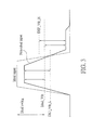
- FIG. 3 illustrates an unrolled DFE control scheme involved with the method 200 shown in FIG. 2 according to an embodiment of the present invention.
- the unrolled DFE control scheme is directed to implementing the apparatus 100 by considering 1 st Tap unrolled DFE as shown in FIG. 3 .
- a previous bit such as the logical value of 0 may be sent through the channel, and the next bit such as the logical value of 1 would be impacted by the channel response, so the swing of the partial waveform corresponding to the next bit cannot reach the ideal swing.
- the waveform corresponding to the ideal input may be varied and may become the waveform corresponding to the non-ideal input, and therefore the ideal voltage threshold Ideal_Vth for the ideal input may be not suitable for the non-ideal input.
- the apparatus 100 may utilize the DFE voltage thresholds DFE_Vth_L and DFE_Vth_H for the non-ideal input. For example, the apparatus 100 may selectively change the DFE voltage thresholds DFE_Vth_L and/or DFE_Vth_H based on previous data.
- a digital code such as that carried by the tap control signal TAP_ctrl or that carried by the offset control signal OS_ctrl may be sent toward an analog DAC such as one of the DACs mentioned above, so the information may be transferred, through the associated wirings mentioned above, toward every comparator of the aforementioned comparators that requires DFE (more particularly, requires the DFE information to be applied to this comparator) to cancel the ISI effect.
- the signal strength related to a specific threshold voltage may be enhanced during such a process.
- FIG. 4 illustrates a half-rate unrolled 1st tap DFE architecture involved with the method 200 shown in FIG. 2 according to an embodiment of the present invention, where the half-rate unrolled 1 st tap DFE architecture shown in FIG. 4 can be taken as an example of at least one portion of the apparatus 100 shown in FIG. 1 .
- the DACs 410, 420-1, 420-2, 420-3, 420-4, 420-5, and 420-6 can be taken as an example of the plurality of DACs mentioned above, the comparators 430-1, 430-2, 430-3, and 430-4 (labeled "Comp.” in FIG.
- comparators 118-1 for data recovery
- comparators 430-5 and 430-6 labeled "Comp.” in FIG. 4 , for brevity
- Comparators 118-2 for error detection
- a set of broadcasting wirings 418-1, 418-2, 418-3, 418-4, 418-5, and 418-6 between the buffers 412P and 412N and the DACs 420-1, 420-2, 420-3, 420-4, 420-5, and 420-6 can be taken as an example of the associated broadcasting wirings mentioned above, while another set of broadcasting wirings 428-1, 428-2, 428-3, 428-4, 428-5, and 428-6 between the DACs 420-1, 420-2, 420-3, 420-4, 420-5, and 420-6 and the comparators 430-1, 430-2, 430-3, 430-4, 430-5, and 430-6 can be taken as another example of the associated broadcasting wirings mentioned above.
- the half-rate unrolled 1 st tap DFE architecture may further comprise some multiplexers (labeled "MUX" in FIG. 4 , for brevity).
- the apparatus 100 may utilize a DAC 410 to perform digital-to-analog conversion on the tap control signal TAP_ctrl to generate analog outputs at the two DAC output terminals P and N of this DAC 410, respectively.
- the buffers 412P and 412N are coupled to the two DAC output terminals P and N, respectively, and are arranged for buffering the analog outputs output from the two DAC output terminals P and N of the DAC 410.
- the information broadcasting and calculation circuit 110 may broadcast the DFE coefficients toward the comparators 430-1, 430-2, 430-3, 430-4, 430-5 and 430-6.
- the information broadcasting and calculation circuit 110 may perform voltage summation by applying the DFE coefficients, i.e. the DFE coefficients represented by the analog outputs output from the two DAC output terminals P and N, to two voltage reference terminals ⁇ VH, VL ⁇ (e.g.
- the information broadcasting and calculation circuit 110 may broadcast the offset toward the comparators 430-1, 430-2, 430-3, 430-4, 430-5 and 430-6.
- the information broadcasting and calculation circuit 110 may perform current summation by applying the offset represented by the offset control signal OS_ctrl to another voltage reference terminal VS of the aforementioned each DAC of the DACs 420-1, 420-2, 420-3, 420-4, 420-5, and 420-6 through a broadcasting wiring of the other set of broadcasting wirings 428-1, 428-2, 428-3, 428-4, 428-5, and 428-6.
- the offset control signal OS_ctrl may perform current summation by applying the offset represented by the offset control signal OS_ctrl to another voltage reference terminal VS of the aforementioned each DAC of the DACs 420-1, 420-2, 420-3, 420-4, 420-5, and 420-6 through a broadcasting wiring of the other set of broadcasting wirings 428-1, 428-2, 428-3, 428-4, 428-5, and 428-6.
- the information broadcasting and calculation circuit 110 may broadcast the DFE information respectively corresponding to the tap control signal TAP_ctrl and the offset control signal OS_ctrl toward the two sets of comparators 118-1 and 118-2 such as the comparators ⁇ 430-1, 430-2, 430-3, 430-4 ⁇ and ⁇ 430-5, 430-6 ⁇ , respectively, where a mathematical expression of the comparison results of the comparators ⁇ 430-1, 430-2, 430-3, 430-4, 430-5, 430-6 ⁇ (or the derivatives thereof) may be expressed as follows:
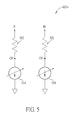
- FIG. 5 illustrates some components within a DAC within some of the DACs shown in FIG. 4 according to an embodiment of the present invention.
- each DAC of a portion of the plurality of DACs such as any DAC 420-i within the DACs 420-1, 420-2, 420-3, 420-4, 420-5, and 420-6 shown in FIG. 4 (e.g.
- the index i may be a positive integer that falls within the range of the interval [1, 6] in some embodiments), may comprise a first resistor 512 having a first terminal coupled to the high voltage reference terminal VH of this DAC 420-i, a first variable current source 514 coupled between a second terminal of the first resistor 512 and one ground terminal within at least one ground terminal (e.g. one or more ground terminals) of this DAC 420-i, a second resistor 522 having a first terminal coupled to the low voltage reference terminal VL of this DAC 420-i, and a second variable current source 524 coupled between a second terminal of the second resistor 522 and one ground terminal within the aforementioned at least one ground terminal of this DAC 420-i.
- a first resistor 512 having a first terminal coupled to the high voltage reference terminal VH of this DAC 420-i
- a first variable current source 514 coupled between a second terminal of the first resistor 512 and one ground terminal within at least one ground terminal (e.g
- a terminal between the first resistor 512 and the first variable current source 514 is the output terminal of the first variable current source 512, and can be utilized as the output terminal OP of this DAC 420-i.
- a terminal between the second resistor 522 and the second variable current source 524 is the output terminal of the second variable current source 522, and can be utilized as the output terminal ON of this DAC 420-i.
- a current control terminal of each current source within the first variable current source 514 and the second variable current source 524 may be coupled to the voltage reference terminal VS of this DAC 420-i and may be controlled by the offset control signal OS_ctrl.
- this DAC 420-i may control the offset according to the offset control signal OS_ctrl with aid of the first variable current source 514 and the second variable current source 524, and more particularly may adjust the offset compensation amount applied to the input signal IN through the next stage (i.e. the corresponding comparator 430-i within the comparators ⁇ 430-1, 430-2, 430-3, 430-4, 430-5, 430-6 ⁇ ).
- each voltage reference terminal within the two voltage reference terminals ⁇ VH, VL ⁇ may be controlled by the tap control signal TAP_ctrl through the upper half of the architecture shown in FIG. 4 .
- this DAC 420-i may control the tap coefficients, and more particularly may adjust the voltage threshold used for comparing the input signal IN through the next stage (i.e. the corresponding comparator 430-i within the comparators ⁇ 430-1, 430-2, 430-3, 430-4, 430-5, 430-6 ⁇ ).
- the DAC 420-i may take the broadcasted information as common information. This is for illustrative purposes only, and is not meant to be a limitation of the present invention. According to some embodiments of the present invention, each sampler may have their own offset as well, so the DAC 420-i of these embodiments may also adjusts its level based on one or more dedicated comparator offset levels. This is for illustrative purposes only, and is not meant to be a limitation of the present invention.
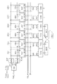
- FIG. 6 illustrates a half-rate unrolled 1st tap DFE architecture involved with the method 200 shown in FIG. 2 according to another embodiment of the present invention, where the half-rate unrolled 1st tap DFE architecture shown in FIG. 6 can be taken as an example of at least one portion (e.g. a portion or all) of the apparatus 100 shown in FIG. 1 .
- the half-rate unrolled 1st tap DFE architecture shown in FIG. 4 it is unnecessary to implement the buffers 412P and 412N in this embodiment.
- Similar descriptions for this embodiment are not repeated in detail here.
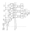
- FIG. 7 illustrates a full-rate unrolled 1st tap DFE architecture involved with the method 200 shown in FIG. 2 according to another embodiment of the present invention, where the full-rate unrolled 1st tap DFE architecture shown in FIG. 7 can be taken as an example of at least one portion (e.g. a portion or all) of the apparatus 100 shown in FIG. 1 .
- the half-rate unrolled 1st tap DFE architecture shown in FIG. 7 can be taken as an example of at least one portion (e.g. a portion or all) of the apparatus 100 shown in FIG. 1 .
- the full-rate unrolled 1st tap DFE architecture of this embodiment may further comprise a latch (labeled "L" in FIG. 7 , for brevity) coupled to the multiplexer corresponding to the comparators 430-1 and 430-2.
Landscapes
- Engineering & Computer Science (AREA)
- Power Engineering (AREA)
- Computer Networks & Wireless Communication (AREA)
- Signal Processing (AREA)
- Analogue/Digital Conversion (AREA)
- Cable Transmission Systems, Equalization Of Radio And Reduction Of Echo (AREA)
- Dc Digital Transmission (AREA)
Abstract
Description
- The present invention relates to a method and apparatus for performing loop unrolled decision feedback equalization (DFE) according to the pre-characterizing clauses of
claims 1 and 11. - According to the related art, in order to overcome the inter symbol interference (ISI) caused by channel loss, a conventional receiver of a conventional system is typically implemented in a manner of changing the sampling threshold to increase the signal-to-noise ratio (SNR), and more particularly, by adopting a speculative DFE structure, the conventional receiver may sample data with different thresholds (e.g. thresholds LEV_H or LEV_L) at different time points to compensate 1 st post cursor (or TAP1) based on previous data, and some problems may occur. For example, the conventional receiver may erroneously reproduce data when receiving a signal. In another example, the conventional receiver may easily fail to recover data in a situation where heavy ISI is encountered, which may degrade the overall performance of the whole conventional system. Thus, how to improve the data recovery capability of a DFE receiver in a system, in order to guarantee the overall performance of the whole system, has become an important issue to be solved.
- This in mind, the present invention aims at providing a method for performing loop unrolled decision feedback equalization (DFE) in an electronic device and an associated apparatus that automatically adjust equalization information input into comparators within a receiver such as a DFE receiver, and/or adaptively adjust equalization information input into comparators within a receiver such as a DFE receiver with aid of voltage feedforward.
- This is achieved by a method and apparatus according to
claims 1 and 11. The dependent claims pertain to corresponding further developments and improvements. - In one aspect, the disclosure features a method for performing loop unrolled decision feedback equalization in an electronic device, where the method comprises the steps of: receiving a tap control signal and an offset control signal from a digital domain of a DFE receiver in the electronic device, and generating DFE information respectively corresponding to the tap control signal and the offset control signal in an analog domain of the DFE receiver; broadcasting the DFE information respectively corresponding to the tap control signal and the offset control signal toward a plurality of comparators in the DFE receiver; utilizing the plurality of comparators to perform comparison operations according to the DFE information respectively corresponding to the tap control signal and the offset control signal to generate a plurality of comparison results; and selectively adjusting the tap control signal and the offset control signal according to the plurality of comparison results, in order to control (more particularly, optimize) the DFE information respectively corresponding to the tap control signal and the offset control signal, respectively.
- In one aspect, the disclosure features an apparatus for performing loop unrolled decision feedback equalization in an electronic device, where the apparatus comprises at least one portion of the electronic device. The apparatus may comprise information broadcasting and calculation circuit and a controller that is coupled to the information broadcasting and calculation circuit. The information broadcasting and calculation circuit is arranged for receiving a tap control signal and an offset control signal from a digital domain of a DFE receiver in the electronic device and generating DFE information respectively corresponding to the tap control signal and the offset control signal in an analog domain of the DFE receiver, broadcasting the DFE information respectively corresponding to the tap control signal and the offset control signal toward a plurality of comparators in the DFE receiver, and utilizing the plurality of comparators to perform comparison operations according to the DFE information respectively corresponding to the tap control signal and the offset control signal to generate a plurality of comparison results. In addition, the controller is arranged for selectively adjusting the tap control signal and the offset control signal according to the plurality of comparison results, in order to control (more particularly, optimize) the DFE information respectively corresponding to the tap control signal and the offset control signal, respectively.
- It is an advantage of the present invention that the present invention method and the associated apparatus can enhance the overall performance of a system comprising the electronic device. In addition, the present invention method and the associated apparatus can automatically adjust equalization information input into comparators within a receiver such as a DFE receiver. As a result, the related art problems (e.g. the problem of erroneously reproducing data when receiving a signal, and the problem of failing to recover data in a situation where heavy ISI is encountered) can be resolved. Additionally, the present invention method and the associated apparatus can adaptively adjust equalization information input into comparators within a receiver such as a DFE receiver with aid of voltage feedforward, and therefore can precisely track the waveforms of the received signal of the DFE receiver and correctly recover the data.
- In the following, the invention is further illustrated by way of example, taking reference to the accompanying drawings. Thereof
- FIG. 1
- is a diagram of an apparatus for performing loop unrolled decision feedback equalization (DFE) in an electronic device according to a first embodiment of the present invention,
- FIG. 2
- illustrates a flowchart of a method for performing loop unrolled DFE in an electronic device according to an embodiment of the present invention,
- FIG. 3
- illustrates an unrolled DFE control scheme involved with the method shown in
FIG. 2 according to an embodiment of the present invention, - FIG. 4
- illustrates a half-rate unrolled 1st tap DFE architecture involved with the method shown in
FIG. 2 according to an embodiment of the present invention, - FIG. 5
- illustrates some components within a digital-to-analog converter (DAC) within some of the DACs shown in
FIG. 4 according to an embodiment of the present invention, - FIG. 6
- illustrates a half-rate unrolled 1st tap DFE architecture involved with the method shown in
FIG. 2 according to another embodiment of the present invention, and - FIG. 7
- illustrates a full-rate unrolled 1st tap DFE architecture involved with the method shown in
FIG. 2 according to another embodiment of the present invention. - Certain terms are used throughout the following description and claims, which refer to particular components. As one skilled in the art will appreciate, electronic equipment manufacturers may refer to a component by different names. This document does not intend to distinguish between components that differ in name but not in function. In the following description and in the claims, the terms "include" and "comprise" are used in an open-ended fashion, and thus should be interpreted to mean "include, but not limited to ...". Also, the term "couple" is intended to mean either an indirect or direct electrical connection. Accordingly, if one device is coupled to another device, that connection may be through a direct electrical connection, or through an indirect electrical connection via other devices and connections.
-
FIG. 1 is a diagram of anapparatus 100 for performing loop unrolled decision feedback equalization (DFE) in an electronic device according to a first embodiment of the present invention, where theapparatus 100 may comprise at least one portion of the electronic device. For example, theapparatus 100 may comprise a portion of the electronic device mentioned above, and more particularly, can be at least one hardware circuit such as at least one integrated circuit (IC) within the electronic device and associated circuits thereof. In another example, theapparatus 100 can be the whole of the electronic device mentioned above. In another example, theapparatus 100 may comprise a system comprising the electronic device mentioned above (e.g. a wireless communications system comprising the electronic device). Examples of the electronic device may include, but not limited to, a mobile phone, a tablet, and a laptop computer. - As shown in
FIG. 1 , theapparatus 100 may comprise an information broadcasting andcalculation circuit 110 and acontroller 120, where an information broadcasting module within the information broadcasting andcalculation circuit 110 may comprise a plurality of digital-to-analog converters (DACs) and associated broadcasting wirings. For example, the information broadcasting andcalculation circuit 110 may comprise a DFEcoefficient setting module 112, anoffset setting module 114, a plurality of arithmetic calculation modules such as two arithmetic calculation modules 116-1 and 116-2, and a plurality of comparators such as two sets of comparators 118-1 and 118-2 (respectively labeled "Comparator for Data Recovery" and "Comparator for Error Detection" inFIG. 1 , for better comprehension), in which the set of comparators 118-1 may be utilized for performing data recovery and the set of comparators 118-2 may be utilized for performing error detection. The plurality of DACs and the associated broadcasting wirings of the information broadcasting module mentioned above may be implemented with some modules (or some components) and some wirings within the information broadcasting andcalculation circuit 110. More particularly, in a situation where this information broadcasting module is arranged for broadcasting DFE information toward the plurality of comparators, the information broadcasting module may comprise the DFEcoefficient setting module 112, theoffset setting module 114, and the plurality of arithmetic calculation modules such as the two arithmetic calculation modules 116-1 and 116-2. In addition, theapparatus 100 may further comprise an analog front end (AFE)circuit 130. For example, the components of the architecture shown inFIG. 1 may be positioned within a receiver such as a DFE receiver in the electronic device, and theAFE circuit 130 may be regarded as the AFE circuit of the DFE receiver, for receiving an input signal of the DFE receiver. - According to this embodiment, the
AFE circuit 130 may receive a pad input signal PAD_IN, which can be taken as an example of the input signal of the DFE receiver, and may perform front end processing on the pad input signal PAD_IN to generate a corresponding input signal IN, and may further input the corresponding input signal IN into the information broadcasting andcalculation circuit 110. In addition, the information broadcasting andcalculation circuit 110 may utilize the DFEcoefficient setting module 112 and theoffset setting module 114 to set a plurality of DFE coefficients of the DFE receiver and an offset of the DFE receiver, respectively, and may utilize the plurality of comparators to generate a plurality of comparison results, where the plurality of comparison results and/or some derivatives of the plurality of comparison results may be input into thecontroller 120. For example, the DFEcoefficient setting module 112 may set the DFE coefficients with a predetermined initial value of these DFE coefficients, and theoffset setting module 114 may set the offset with a predetermined initial value of the offset. Additionally, thecontroller 120 may determine whether to adjust these DFE coefficients and determine whether to adjust the offset according to at least one portion of the outputs of the information broadcasting andcalculation circuit 110, such as the plurality of comparison results and/or the derivatives of the plurality of comparison results. More particularly, by setting (or by changing) the tap control signal TAP_ctrl and the offset control signal OS_ctrl, thecontroller 120 may selectively adjust the DFE coefficients and selectively adjust the offset at any time when needed. As a result, the DFE coefficients and the offset may be adjusted iteratively. - Based upon the architecture shown in
FIG. 1 , theapparatus 100 can adaptively adjust equalization information, such as the DFE coefficients and the offset that are applied to (or indirectly input into) the plurality of comparators positioned in the receiver (e.g. the DFE receiver), with aid of voltage feedforward. Therefore, theapparatus 100 can precisely track the waveforms of the received signal of the DFE receiver (e.g. the pad input signal PAD_IN) and correctly recover the data carried by the received signal. -
FIG. 2 illustrates a flowchart of amethod 200 for performing loop unrolled DFE in an electronic device according to an embodiment of the present invention. Themethod 200 shown inFIG. 2 can be applied to theapparatus 100 shown inFIG. 1 , and can be applied to theinformation broadcasting circuit 110 and thecontroller 120 thereof. The method can be described as follows. - In
Step 210, the information broadcasting and calculation circuit 110 (more particularly, the information broadcasting module thereof) may receive the tap control signal TAP_ctrl and the offset control signal OS_ctrl from a digital domain of the DFE receiver in the electronic device, and generate DFE information respectively corresponding to the tap control signal TAP_ctrl and the offset control signal OS_ctrl in an analog domain of the DFE receiver. For example, the DFE information corresponding to the tap control signal TAP_ctrl may comprise the DFE coefficients, and the DFE information corresponding to the offset control signal OS_ctrl may comprise the offset. According to this embodiment, the tap control signal TAP_ctrl and the offset control signal OS_ctrl may be generated by thecontroller 120 in the digital domain of the DFE receiver, and the information broadcasting andcalculation circuit 110 is positioned in the analog domain of the DFE receiver. - In
Step 220, the information broadcasting and calculation circuit 110 (more particularly, the information broadcasting module thereof) may broadcast the DFE information respectively corresponding to the tap control signal TAP_ctrl and the offset control signal OS_ctrl toward the plurality of comparators in the DFE receiver, such as the two sets of comparators 118-1 and 118-2 in the DFE receiver. For example, in a situation where the DFE information corresponding to the tap control signal TAP_ctrl comprises the DFE coefficients and the DFE information corresponding to the offset control signal OS_ctrl comprises the offset, theapparatus 100 may utilize the information broadcasting and calculation circuit 110 (more particularly, the information broadcasting module thereof) to broadcast the DFE coefficients toward at least one set (e.g. one or more sets) within the two sets of comparators 118-1 and 118-2 and broadcast the offset toward at least one set (e.g. one or more sets) within the two sets of comparators 118-1 and 118-2. - In
Step 230, the information broadcasting and calculation circuit 110 (more particularly, the two sets of comparators 118-1 and 118-2) may perform comparison operations according to the DFE information respectively corresponding to the tap control signal TAP_ctrl and the offset control signal OS_ctrl, to generate multiple comparison results such as the plurality of comparison results. - In
Step 240, thecontroller 120 may selectively adjust the tap control signal TAP_ctrl and the offset control signal OS_ctrl according to the comparison results mentioned inStep 230, such as the plurality of comparison results, in order to control (more particularly, optimize) the DFE information respectively corresponding to the tap control signal TAP_ctrl and the offset control signal OS_ctrl (e.g. the DFE coefficients and the offset), respectively. For example, thecontroller 120 may selectively adjust the tap control signal TAP_ctrl and the offset control signal OS_ctrl according to the plurality of comparison results and/or the derivatives of the plurality of comparison results, in order to control (more particularly, optimize) the DFE information respectively corresponding to the tap control signal TAP_ctrl and the offset control signal OS_ctrl (e.g. the DFE coefficients and the offset), respectively. - Please note that the operation of
Step 210, the operation ofStep 220, the operation ofStep 230, and the operation ofStep 240 are illustrated inFIG. 2 , respectively. This is for illustrative purposes only, and is not meant to be a limitation of the present invention. According to some variations of this embodiment, at least one portion of the operation ofStep 210, at least one portion of the operation ofStep 220, at least one portion of the operation ofStep 230, and/or at least one portion (e.g. a portion or all) of the operation ofStep 240 can be performed at the same time. - Based upon the working flow of the
method 200, the apparatus 100 (more particularly, the controller 120) may control (more particularly, optimize) the DFE information respectively corresponding to the tap control signal TAP_ctrl and the offset control signal OS_ctrl (e.g. the DFE coefficients and the offset) by adjusting the tap control signal TAP_ctrl and the offset control signal OS_ctrl according to the comparison results mentioned in Step 230 (e.g. the plurality of comparison results) in an online manner, respectively. For example, the initial states of the tap control signal TAP_ctrl and the offset control signal OS_ctrl may be set arbitrarily, and thecontroller 120 may adaptively adjust the DFE information respectively corresponding to the tap control signal TAP_ctrl and the offset control signal OS_ctrl (e.g. the DFE coefficients and the offset) in response to the variations of characteristics of the input signal of the DFE receiver (e.g. the variations of the swings corresponding to some data pattern carried by this input signal, and/or the variations of the voltage level range of this input signal), since thecontroller 120 may selectively adjust the tap control signal TAP_ctrl and the offset control signal OS_ctrl according to the comparison results mentioned inStep 230 when needed. - According to this embodiment, the
apparatus 100 may utilize the DFEcoefficient setting module 112 to set the plurality of DFE coefficients with a predetermined initial value of these DFE coefficients, and may utilize the offsetsetting module 114 to set the offset with a predetermined initial value of the offset. More particularly, by setting (or by changing) the tap control signal TAP_ctrl, thecontroller 120 may selectively adjust the plurality of DFE coefficients through the DFEcoefficient setting module 112 at any time when needed. By setting (or by changing) the offset control signal OS_ctrl, thecontroller 120 may selectively adjust the offset through the offsetsetting module 114 at any time when needed. As a result, the DFE coefficients and the offset may be optimized. -
FIG. 3 illustrates an unrolled DFE control scheme involved with themethod 200 shown inFIG. 2 according to an embodiment of the present invention. The unrolled DFE control scheme is directed to implementing theapparatus 100 by considering 1st Tap unrolled DFE as shown inFIG. 3 . For example, a previous bit such as the logical value of 0 may be sent through the channel, and the next bit such as the logical value of 1 would be impacted by the channel response, so the swing of the partial waveform corresponding to the next bit cannot reach the ideal swing. As a result, the waveform corresponding to the ideal input may be varied and may become the waveform corresponding to the non-ideal input, and therefore the ideal voltage threshold Ideal_Vth for the ideal input may be not suitable for the non-ideal input. By applying the unrolled DFE control scheme, theapparatus 100 may utilize the DFE voltage thresholds DFE_Vth_L and DFE_Vth_H for the non-ideal input. For example, theapparatus 100 may selectively change the DFE voltage thresholds DFE_Vth_L and/or DFE_Vth_H based on previous data. A digital code such as that carried by the tap control signal TAP_ctrl or that carried by the offset control signal OS_ctrl may be sent toward an analog DAC such as one of the DACs mentioned above, so the information may be transferred, through the associated wirings mentioned above, toward every comparator of the aforementioned comparators that requires DFE (more particularly, requires the DFE information to be applied to this comparator) to cancel the ISI effect. As a result, the signal strength related to a specific threshold voltage may be enhanced during such a process. -
FIG. 4 illustrates a half-rate unrolled 1st tap DFE architecture involved with themethod 200 shown inFIG. 2 according to an embodiment of the present invention, where the half-rate unrolled 1 st tap DFE architecture shown inFIG. 4 can be taken as an example of at least one portion of theapparatus 100 shown inFIG. 1 . For example, theDACs 410, 420-1, 420-2, 420-3, 420-4, 420-5, and 420-6 can be taken as an example of the plurality of DACs mentioned above, the comparators 430-1, 430-2, 430-3, and 430-4 (labeled "Comp." inFIG. 4 , for brevity) can be taken as an example of the set of comparators 118-1 for data recovery, and the comparators 430-5 and 430-6 (labeled "Comp." inFIG. 4 , for brevity) can be taken as an example of the set of comparators 118-2 for error detection. In another example, a set of broadcasting wirings 418-1, 418-2, 418-3, 418-4, 418-5, and 418-6 between thebuffers FIG. 4 , the half-rate unrolled 1 st tap DFE architecture may further comprise some multiplexers (labeled "MUX" inFIG. 4 , for brevity). - According to this embodiment, the
apparatus 100 may utilize aDAC 410 to perform digital-to-analog conversion on the tap control signal TAP_ctrl to generate analog outputs at the two DAC output terminals P and N of thisDAC 410, respectively. Thebuffers DAC 410. By utilizing the set of broadcasting wirings 418-1, 418-2, 418-3, 418-4, 418-5, and 418-6, the information broadcasting andcalculation circuit 110 may broadcast the DFE coefficients toward the comparators 430-1, 430-2, 430-3, 430-4, 430-5 and 430-6. For example, the information broadcasting andcalculation circuit 110 may perform voltage summation by applying the DFE coefficients, i.e. the DFE coefficients represented by the analog outputs output from the two DAC output terminals P and N, to two voltage reference terminals {VH, VL} (e.g. the high voltage reference terminal VH arranged for inputting a high voltage level reference, and the low voltage reference terminal VL arranged for inputting a low voltage level reference) of each DAC of the DACs 420-1, 420-2, 420-3, 420-4, 420-5, and 420-6 through a broadcasting wiring of the set of broadcasting wirings 418-1, 418-2, 418-3, 418-4, 418-5, and 418-6, respectively. In addition, by utilizing the other set of broadcasting wirings 428-1, 428-2, 428-3, 428-4, 428-5, and 428-6, the information broadcasting andcalculation circuit 110 may broadcast the offset toward the comparators 430-1, 430-2, 430-3, 430-4, 430-5 and 430-6. For example, the information broadcasting andcalculation circuit 110 may perform current summation by applying the offset represented by the offset control signal OS_ctrl to another voltage reference terminal VS of the aforementioned each DAC of the DACs 420-1, 420-2, 420-3, 420-4, 420-5, and 420-6 through a broadcasting wiring of the other set of broadcasting wirings 428-1, 428-2, 428-3, 428-4, 428-5, and 428-6. As a result of utilizing the half-rate unrolled 1st tap DFE architecture shown inFIG. 4 , the information broadcasting andcalculation circuit 110 may broadcast the DFE information respectively corresponding to the tap control signal TAP_ctrl and the offset control signal OS_ctrl toward the two sets of comparators 118-1 and 118-2 such as the comparators {430-1, 430-2, 430-3, 430-4} and {430-5, 430-6}, respectively, where a mathematical expression of the comparison results of the comparators {430-1, 430-2, 430-3, 430-4, 430-5, 430-6} (or the derivatives thereof) may be expressed as follows: - (IN - OS_ctrl - TAP_ctrl > 0 ?)
-
FIG. 5 illustrates some components within a DAC within some of the DACs shown inFIG. 4 according to an embodiment of the present invention. For example, each DAC of a portion of the plurality of DACs, such as any DAC 420-i within the DACs 420-1, 420-2, 420-3, 420-4, 420-5, and 420-6 shown inFIG. 4 (e.g. the index i may be a positive integer that falls within the range of the interval [1, 6] in some embodiments), may comprise afirst resistor 512 having a first terminal coupled to the high voltage reference terminal VH of this DAC 420-i, a first variablecurrent source 514 coupled between a second terminal of thefirst resistor 512 and one ground terminal within at least one ground terminal (e.g. one or more ground terminals) of this DAC 420-i, asecond resistor 522 having a first terminal coupled to the low voltage reference terminal VL of this DAC 420-i, and a second variablecurrent source 524 coupled between a second terminal of thesecond resistor 522 and one ground terminal within the aforementioned at least one ground terminal of this DAC 420-i. Please note that a terminal between thefirst resistor 512 and the first variable current source 514 (e.g. the upper terminal of the first variablecurrent source 514 shown inFIG. 5 ) is the output terminal of the first variablecurrent source 512, and can be utilized as the output terminal OP of this DAC 420-i. In addition, a terminal between thesecond resistor 522 and the second variable current source 524 (e.g. the upper terminal of the second variablecurrent source 524 shown inFIG. 5 ) is the output terminal of the second variablecurrent source 522, and can be utilized as the output terminal ON of this DAC 420-i. - According to this embodiment, a current control terminal of each current source within the first variable
current source 514 and the second variablecurrent source 524 may be coupled to the voltage reference terminal VS of this DAC 420-i and may be controlled by the offset control signal OS_ctrl. As a result, this DAC 420-i may control the offset according to the offset control signal OS_ctrl with aid of the first variablecurrent source 514 and the second variablecurrent source 524, and more particularly may adjust the offset compensation amount applied to the input signal IN through the next stage (i.e. the corresponding comparator 430-i within the comparators {430-1, 430-2, 430-3, 430-4, 430-5, 430-6}). In addition, each voltage reference terminal within the two voltage reference terminals {VH, VL} may be controlled by the tap control signal TAP_ctrl through the upper half of the architecture shown inFIG. 4 . As a result, this DAC 420-i may control the tap coefficients, and more particularly may adjust the voltage threshold used for comparing the input signal IN through the next stage (i.e. the corresponding comparator 430-i within the comparators {430-1, 430-2, 430-3, 430-4, 430-5, 430-6}). - In this embodiment, the DAC 420-i may take the broadcasted information as common information. This is for illustrative purposes only, and is not meant to be a limitation of the present invention. According to some embodiments of the present invention, each sampler may have their own offset as well, so the DAC 420-i of these embodiments may also adjusts its level based on one or more dedicated comparator offset levels. This is for illustrative purposes only, and is not meant to be a limitation of the present invention.
-
FIG. 6 illustrates a half-rate unrolled 1st tap DFE architecture involved with themethod 200 shown inFIG. 2 according to another embodiment of the present invention, where the half-rate unrolled 1st tap DFE architecture shown inFIG. 6 can be taken as an example of at least one portion (e.g. a portion or all) of theapparatus 100 shown inFIG. 1 . In comparison with the half-rate unrolled 1st tap DFE architecture shown inFIG. 4 , it is unnecessary to implement thebuffers -
FIG. 7 illustrates a full-rate unrolled 1st tap DFE architecture involved with themethod 200 shown inFIG. 2 according to another embodiment of the present invention, where the full-rate unrolled 1st tap DFE architecture shown inFIG. 7 can be taken as an example of at least one portion (e.g. a portion or all) of theapparatus 100 shown inFIG. 1 . In comparison with the half-rate unrolled 1st tap DFE architecture shown inFIG. 4 , it is unnecessary to implement, in the full-rate unrolled 1st tap DFE architecture of this embodiment, the broadcasting wirings 418-3, 418-4, and 418-6, the DACs 420-3, 420-4, and 420-6, the broadcasting wirings 428-3, 428-4, and 428-6, the comparators 430-3, 430-4, and 430-6, and the multiplexer corresponding to the comparators 430-3 and 430-4. In addition, the full-rate unrolled 1 st tap DFE architecture of this embodiment may further comprise a latch (labeled "L" inFIG. 7 , for brevity) coupled to the multiplexer corresponding to the comparators 430-1 and 430-2. As the detailed components and connections (or wirings) have been illustrated inFIG. 7 , those skilled in the art may easily understand the implementation of full-rate unrolled 1st tap DFE architecture and the operations thereof based upon the descriptions of the above embodiments. Therefore, similar descriptions for this embodiment are not repeated in detail here. - All combinations and sub-combinations of above-described features also belong to the invention.
Claims (11)
- A method for performing loop unrolled decision feedback equalization (DFE) in an electronic device (100), characterized in that the method comprises the steps of:receiving a tap control signal and an offset control signal from a digital domain of a DFE receiver in the electronic device (100), and generating DFE information respectively corresponding to the tap control signal and the offset control signal in an analog domain of the DFE receiver;broadcasting the DFE information respectively corresponding to the tap control signal and the offset control signal toward a plurality of comparators (118-1, 118-2, 430-1, 430-2, 430-3, 430-4, 430-5, 430-6) in the DFE receiver;utilizing the plurality of comparators (118-1, 118-2, 430-1, 430-2, 430-3, 430-4, 430-5, 430-6) to perform comparison operations according to the DFE information respectively corresponding to the tap control signal and the offset control signal to generate a plurality of comparison results; andselectively adjusting the tap control signal and the offset control signal according to the plurality of comparison results, in order to control the DFE information respectively corresponding to the tap control signal and the offset control signal, respectively.
- The method of claim 1, characterized in that the DFE information corresponding to the tap control signal comprises a plurality of DFE coefficients of the DFE receiver; and the DFE information corresponding to the offset control signal comprises an offset of the DFE receiver.
- The method of claim 2, characterized in that the method further comprises:utilizing a DFE coefficient setting module (112) to set the plurality of DFE coefficients with a predetermined initial value of the plurality of DFE coefficients;wherein the step of selectively adjusting the tap control signal and the offset control signal according to the plurality of comparison results in order to control the DFE information respectively corresponding to the tap control signal and the offset control signal respectively further comprises:by changing the tap control signal, selectively adjusting the plurality of DFE coefficients through the DFE coefficient setting module (112).
- The method of claim 2, characterized in that the method further comprises:utilizing an offset setting module (114) to set the offset with a predetermined initial value of the offset;wherein the step of selectively adjusting the tap control signal and the offset control signal according to the plurality of comparison results in order to control the DFE information respectively corresponding to the tap control signal and the offset control signal respectively further comprises:by changing the offset control signal, selectively adjusting the offset through the offset setting module (114).
- The method of claim 2, characterized in that the step of broadcasting the DFE information respectively corresponding to the tap control signal and the offset control signal toward the plurality of comparators in the DFE receiver further comprises:utilizing a digital-to-analog converter (DAC) (410) of a plurality of DACs (410, 420-1, 420-2, 420-3, 420-4, 420-5, 420-6) to perform digital-to-analog conversion on the tap control signal to generate analog outputs of the DAC (410), and outputting the analog outputs from two DAC output terminals of the DAC (410), respectively, wherein the analog outputs represent the DFE coefficients;utilizing a set of broadcasting wirings (418-1, 418-2, 418-3, 418-4, 418-5, 418-6) to broadcast the DFE coefficients toward the plurality of comparators (430-1, 430-2, 430-3, 430-4, 430-5, 430-6) through other DACs (420-1, 420-2, 420-3, 420-4, 420-5, 420-6) of the plurality of DACs (410, 420-1, 420-2, 420-3, 420-4, 420-5, 420-6), respectively;utilizing another set of broadcasting wirings (428-1, 428-2, 428-3, 428-4, 428-5, 428-6) to broadcast the offset toward the plurality of comparators (430-1, 430-2, 430-3, 430-4, 430-5, 430-6) through the other DACs (420-1, 420-2, 420-3, 420-4, 420-5, 420-6) of the plurality of DACs (410, 420-1, 420-2, 420-3, 420-4, 420-5, 420-6), respectively; andutilizing the other DACs (420-1, 420-2, 420-3, 420-4, 420-5, 420-6) of the plurality of DACs (410, 420-1, 420-2, 420-3, 420-4, 420-5, 420-6) to perform digital-to-analog conversion to generate the plurality of comparison results according to the DFE coefficients and the offset, respectively.
- The method of claim 5, characterized in that the step of utilizing the set of broadcasting wirings (418-1, 418-2, 418-3, 418-4, 418-5, 418-6) to broadcast the DFE coefficients toward the plurality of comparators (430-1, 430-2, 430-3, 430-4, 430-5, 430-6) through the other DACs (420-1, 420-2, 420-3, 420-4, 420-5, 420-6) of the plurality of DACs (410, 420-1, 420-2, 420-3, 420-4, 420-5, 420-6) respectively further comprises:performing voltage summation by applying the DFE coefficients represented by the analog outputs to multiple voltage reference terminals of each DAC of the other DACs (420-1, 420-2, 420-3, 420-4, 420-5, 420-6) of the plurality of DACs (410, 420-1, 420-2, 420-3, 420-4, 420-5, 420-6) through a broadcasting wiring of the set of broadcasting wirings (418-1, 418-2, 418-3, 418-4, 418-5, 418-6), respectively.
- The method of claim 5, characterized in that the step of utilizing the other set of broadcasting wirings (428-1, 428-2, 428-3, 428-4, 428-5, 428-6) to broadcast the offset toward the plurality of comparators (430-1, 430-2, 430-3, 430-4, 430-5, 430-6) through the other DACs (420-1, 420-2, 420-3, 420-4, 420-5, 420-6) of the plurality of DACs (410, 420-1, 420-2, 420-3, 420-4, 420-5, 420-6) respectively further comprises:performing current summation by applying the offset represented by the offset control signal to another voltage reference terminal of each DAC of the other DACs (420-1, 420-2, 420-3, 420-4, 420-5, 420-6) of the plurality of DACs (410, 420-1, 420-2, 420-3, 420-4, 420-5, 420-6) through a broadcasting wiring of the other set of broadcasting wirings (428-1, 428-2, 428-3, 428-4, 428-5, 428-6).
- The method of claim 5, characterized in that each DAC (420-i) of the other DACs (420-1, 420-2, 420-3, 420-4, 420-5, 420-6) of the plurality of DACs (410, 420-1, 420-2, 420-3, 420-4, 420-5, 420-6) comprises:a high voltage reference terminal, arranged for inputting a high voltage level reference;a low voltage reference terminal, arranged for inputting a low voltage level reference;at least one ground terminal;a first resistor (512), having a first terminal coupled to the high voltage reference terminal;a first variable current source (514), coupled between a second terminal of the first resistor (512) and one ground terminal within the at least one ground terminal;a second resistor (522), having a first terminal coupled to the low voltage reference terminal; anda second variable current source (524), coupled between a second terminal of the second resistor (522) and one ground terminal within the at least one ground terminal;wherein a terminal between the first resistor (512) and the first variable current source (514) is utilized as an output terminal of said each DAC (420-i) of the other DACs (420-1, 420-2, 420-3, 420-4, 420-5, 420-6) of the plurality of DACs (410, 420-1, 420-2, 420-3, 420-4, 420-5, 420-6); anda terminal between the second resistor (522) and the second variable current source (524) is utilized as another output terminal of said each DAC (420-i) of the other DACs (420-1, 420-2, 420-3, 420-4, 420-5, 420-6) of the plurality of DACs (410, 420-1, 420-2, 420-3, 420-4, 420-5, 420-6).
- The method of claim 1, characterized in that the step of performing the comparison operations according to the DFE information respectively corresponding to the tap control signal and the offset control signal to generate the plurality of comparison results further comprises:utilizing two sets of comparators (118-1, 118-2, 430-1, 430-2, 430-3, 430-4, 430-5, 430-6) within the plurality of comparators (118-1, 118-2, 430-1, 430-2, 430-3, 430-4, 430-5, 430-6) to perform the comparison operations according to the DFE information respectively corresponding to the tap control signal and the offset control signal to generate the plurality of comparison results, wherein one set of comparators (118-1, 430-1, 430-2, 430-3, 430-4) within the two sets of comparators (118-1, 118-2, 430-1, 430-2, 430-3, 430-4, 430-5, 430-6) is utilized for performing data recovery, and another set of comparators (118-2, 430-5, 430-6) within the two sets of comparators (118-1, 118-2, 430-1, 430-2, 430-3, 430-4, 430-5, 430-6) is utilized for performing error detection.
- The method of claim 1, characterized in that the method further comprises:controlling the DFE information respectively corresponding to the tap control signal and the offset control signal by adjusting the tap control signal and the offset control signal according to the plurality of comparison results in an online manner, respectively.
- An apparatus for performing loop unrolled decision feedback equalization according to any of claims 1-10, wherein the apparatus comprises at least one portion of the electronic device.
Applications Claiming Priority (2)
| Application Number | Priority Date | Filing Date | Title |
|---|---|---|---|
| US201462042881P | 2014-08-28 | 2014-08-28 | |
| US14/737,513 US9479365B2 (en) | 2014-08-28 | 2015-06-12 | Method for performing loop unrolled decision feedback equalization in an electronic device with aid of voltage feedforward, and associated apparatus |
Publications (2)
| Publication Number | Publication Date |
|---|---|
| EP2991297A1 true EP2991297A1 (en) | 2016-03-02 |
| EP2991297B1 EP2991297B1 (en) | 2017-03-08 |
Family
ID=53513956
Family Applications (1)
| Application Number | Title | Priority Date | Filing Date |
|---|---|---|---|
| EP15173083.5A Not-in-force EP2991297B1 (en) | 2014-08-28 | 2015-06-22 | Method for performing loop unrolled decision feedback equalization in an electronic device with aid of voltage feedforward, and associated apparatus |
Country Status (3)
| Country | Link |
|---|---|
| US (1) | US9479365B2 (en) |
| EP (1) | EP2991297B1 (en) |
| CN (1) | CN105391660B (en) |
Families Citing this family (4)
| Publication number | Priority date | Publication date | Assignee | Title |
|---|---|---|---|---|
| KR101794712B1 (en) * | 2016-07-11 | 2017-11-07 | (주) 티엘아이 | Loop un-rolling decision feedback equalization circuit preventing accumulation of errors |
| US11671286B2 (en) | 2018-12-12 | 2023-06-06 | Rambus Inc. | Live offset cancellation of the decision feedback equalization data slicers |
| CN115299013B (en) * | 2020-03-26 | 2024-02-09 | 华为技术有限公司 | Channel tracking method and related equipment thereof |
| KR102853345B1 (en) * | 2020-11-05 | 2025-08-29 | 삼성전자주식회사 | A decision feedback equalizer and a device including same |
Citations (3)
| Publication number | Priority date | Publication date | Assignee | Title |
|---|---|---|---|---|
| US20080049825A1 (en) * | 2006-08-25 | 2008-02-28 | Broadcom Corporation | Equalizer with reorder |
| US20120201289A1 (en) * | 2010-09-13 | 2012-08-09 | Abdalla Mohamed | Decision feedback equalizer and transceiver |
| US20130243070A1 (en) * | 2012-03-16 | 2013-09-19 | Lsi Corporation | Tap adaptation with a fully unrolled decision feedback equalizer |
Family Cites Families (8)
| Publication number | Priority date | Publication date | Assignee | Title |
|---|---|---|---|---|
| US7027503B2 (en) * | 2002-06-04 | 2006-04-11 | Qualcomm Incorporated | Receiver with a decision feedback equalizer and a linear equalizer |
| US8861667B1 (en) * | 2002-07-12 | 2014-10-14 | Rambus Inc. | Clock data recovery circuit with equalizer clock calibration |
| US7397848B2 (en) * | 2003-04-09 | 2008-07-08 | Rambus Inc. | Partial response receiver |
| CN101083642B (en) * | 2006-05-30 | 2010-10-20 | 富士通株式会社 | Systems and methods for adjusting offset compensation applied to a signal |
| US9071478B2 (en) * | 2011-05-24 | 2015-06-30 | Mediatek Inc. | Methods for performing adaptive equalization and associated apparatus |
| US8966353B2 (en) * | 2011-10-31 | 2015-02-24 | Hewlett-Packard Development Company L.P. | Receiver with tap-coefficient adjustments |
| CN102364882A (en) * | 2011-11-18 | 2012-02-29 | 北京航空航天大学 | A Cognitive Radio System Receiver Based on Direct Sequence CDMA-UWB |
| US8861583B2 (en) * | 2012-12-14 | 2014-10-14 | Altera Corporation | Apparatus and methods for equalizer adaptation |
-
2015
- 2015-06-12 US US14/737,513 patent/US9479365B2/en active Active
- 2015-06-22 EP EP15173083.5A patent/EP2991297B1/en not_active Not-in-force
- 2015-08-18 CN CN201510507370.9A patent/CN105391660B/en active Active
Patent Citations (3)
| Publication number | Priority date | Publication date | Assignee | Title |
|---|---|---|---|---|
| US20080049825A1 (en) * | 2006-08-25 | 2008-02-28 | Broadcom Corporation | Equalizer with reorder |
| US20120201289A1 (en) * | 2010-09-13 | 2012-08-09 | Abdalla Mohamed | Decision feedback equalizer and transceiver |
| US20130243070A1 (en) * | 2012-03-16 | 2013-09-19 | Lsi Corporation | Tap adaptation with a fully unrolled decision feedback equalizer |
Also Published As
| Publication number | Publication date |
|---|---|
| US20160065397A1 (en) | 2016-03-03 |
| CN105391660B (en) | 2018-10-12 |
| CN105391660A (en) | 2016-03-09 |
| EP2991297B1 (en) | 2017-03-08 |
| US9479365B2 (en) | 2016-10-25 |
Similar Documents
| Publication | Publication Date | Title |
|---|---|---|
| CN109412585B (en) | Electronic circuit configured to adjust skew between clock signals | |
| US9166844B2 (en) | Receiver with duobinary mode of operation | |
| US7443913B2 (en) | High speed decision feedback equalizer | |
| JP4558028B2 (en) | Clock data recovery device | |
| US8040973B2 (en) | Transmitter including pre-distortion | |
| TW201644241A (en) | Low power high speed receiver with reduced decision feedback equalizer samplers | |
| US8675724B2 (en) | Decision feedback equalizers and operating methods thereof | |
| US11265190B2 (en) | Variable gain amplifier and sampler offset calibration without clock recovery | |
| US12206423B2 (en) | Variable resolution digital equalization | |
| EP2991297B1 (en) | Method for performing loop unrolled decision feedback equalization in an electronic device with aid of voltage feedforward, and associated apparatus | |
| JP2007525061A6 (en) | Partial response receiver | |
| US9071478B2 (en) | Methods for performing adaptive equalization and associated apparatus | |
| US11736265B2 (en) | Horizontal centering of sampling point using vertical vernier | |
| US10778404B1 (en) | Dual-duplex link with asymmetric data rate selectivity | |
| EP3954046B1 (en) | Dynamic integration time adjustment of a clocked data sampler using a static analog calibration circuit | |
| US9148187B2 (en) | Methods and systems for self-referencing single-ended signals | |
| WO2008118714A2 (en) | Circuits, methods and systems for loss-of-signal detection and equalization | |
| US10917130B1 (en) | Signal receiving apparatus and method having anti-RFI mechanism | |
| CN106797354A (en) | transmitter and communication system |
Legal Events
| Date | Code | Title | Description |
|---|---|---|---|
| PUAI | Public reference made under article 153(3) epc to a published international application that has entered the european phase |
Free format text: ORIGINAL CODE: 0009012 |
|
| AK | Designated contracting states |
Kind code of ref document: A1 Designated state(s): AL AT BE BG CH CY CZ DE DK EE ES FI FR GB GR HR HU IE IS IT LI LT LU LV MC MK MT NL NO PL PT RO RS SE SI SK SM TR |
|
| AX | Request for extension of the european patent |
Extension state: BA ME |
|
| 17P | Request for examination filed |
Effective date: 20160331 |
|
| RBV | Designated contracting states (corrected) |
Designated state(s): AL AT BE BG CH CY CZ DE DK EE ES FI FR GB GR HR HU IE IS IT LI LT LU LV MC MK MT NL NO PL PT RO RS SE SI SK SM TR |
|
| 17Q | First examination report despatched |
Effective date: 20160425 |
|
| GRAP | Despatch of communication of intention to grant a patent |
Free format text: ORIGINAL CODE: EPIDOSNIGR1 |
|
| INTG | Intention to grant announced |
Effective date: 20161102 |
|
| GRAS | Grant fee paid |
Free format text: ORIGINAL CODE: EPIDOSNIGR3 |
|
| GRAA | (expected) grant |
Free format text: ORIGINAL CODE: 0009210 |
|
| AK | Designated contracting states |
Kind code of ref document: B1 Designated state(s): AL AT BE BG CH CY CZ DE DK EE ES FI FR GB GR HR HU IE IS IT LI LT LU LV MC MK MT NL NO PL PT RO RS SE SI SK SM TR |
|
| REG | Reference to a national code |
Ref country code: GB Ref legal event code: FG4D |
|
| REG | Reference to a national code |
Ref country code: CH Ref legal event code: EP Ref country code: AT Ref legal event code: REF Ref document number: 874435 Country of ref document: AT Kind code of ref document: T Effective date: 20170315 |
|
| REG | Reference to a national code |
Ref country code: IE Ref legal event code: FG4D |
|
| REG | Reference to a national code |
Ref country code: DE Ref legal event code: R096 Ref document number: 602015001724 Country of ref document: DE |
|
| REG | Reference to a national code |
Ref country code: FR Ref legal event code: PLFP Year of fee payment: 3 |
|
| REG | Reference to a national code |
Ref country code: LT Ref legal event code: MG4D |
|
| REG | Reference to a national code |
Ref country code: NL Ref legal event code: MP Effective date: 20170308 |
|
| PG25 | Lapsed in a contracting state [announced via postgrant information from national office to epo] |
Ref country code: GR Free format text: LAPSE BECAUSE OF FAILURE TO SUBMIT A TRANSLATION OF THE DESCRIPTION OR TO PAY THE FEE WITHIN THE PRESCRIBED TIME-LIMIT Effective date: 20170609 Ref country code: FI Free format text: LAPSE BECAUSE OF FAILURE TO SUBMIT A TRANSLATION OF THE DESCRIPTION OR TO PAY THE FEE WITHIN THE PRESCRIBED TIME-LIMIT Effective date: 20170308 Ref country code: HR Free format text: LAPSE BECAUSE OF FAILURE TO SUBMIT A TRANSLATION OF THE DESCRIPTION OR TO PAY THE FEE WITHIN THE PRESCRIBED TIME-LIMIT Effective date: 20170308 Ref country code: NO Free format text: LAPSE BECAUSE OF FAILURE TO SUBMIT A TRANSLATION OF THE DESCRIPTION OR TO PAY THE FEE WITHIN THE PRESCRIBED TIME-LIMIT Effective date: 20170608 Ref country code: LT Free format text: LAPSE BECAUSE OF FAILURE TO SUBMIT A TRANSLATION OF THE DESCRIPTION OR TO PAY THE FEE WITHIN THE PRESCRIBED TIME-LIMIT Effective date: 20170308 |
|
| REG | Reference to a national code |
Ref country code: AT Ref legal event code: MK05 Ref document number: 874435 Country of ref document: AT Kind code of ref document: T Effective date: 20170308 |
|
| PG25 | Lapsed in a contracting state [announced via postgrant information from national office to epo] |
Ref country code: LV Free format text: LAPSE BECAUSE OF FAILURE TO SUBMIT A TRANSLATION OF THE DESCRIPTION OR TO PAY THE FEE WITHIN THE PRESCRIBED TIME-LIMIT Effective date: 20170308 Ref country code: BG Free format text: LAPSE BECAUSE OF FAILURE TO SUBMIT A TRANSLATION OF THE DESCRIPTION OR TO PAY THE FEE WITHIN THE PRESCRIBED TIME-LIMIT Effective date: 20170608 Ref country code: SE Free format text: LAPSE BECAUSE OF FAILURE TO SUBMIT A TRANSLATION OF THE DESCRIPTION OR TO PAY THE FEE WITHIN THE PRESCRIBED TIME-LIMIT Effective date: 20170308 Ref country code: RS Free format text: LAPSE BECAUSE OF FAILURE TO SUBMIT A TRANSLATION OF THE DESCRIPTION OR TO PAY THE FEE WITHIN THE PRESCRIBED TIME-LIMIT Effective date: 20170308 Ref country code: ES Free format text: LAPSE BECAUSE OF FAILURE TO SUBMIT A TRANSLATION OF THE DESCRIPTION OR TO PAY THE FEE WITHIN THE PRESCRIBED TIME-LIMIT Effective date: 20170308 |
|
| PG25 | Lapsed in a contracting state [announced via postgrant information from national office to epo] |
Ref country code: NL Free format text: LAPSE BECAUSE OF FAILURE TO SUBMIT A TRANSLATION OF THE DESCRIPTION OR TO PAY THE FEE WITHIN THE PRESCRIBED TIME-LIMIT Effective date: 20170308 |
|
| PG25 | Lapsed in a contracting state [announced via postgrant information from national office to epo] |
Ref country code: EE Free format text: LAPSE BECAUSE OF FAILURE TO SUBMIT A TRANSLATION OF THE DESCRIPTION OR TO PAY THE FEE WITHIN THE PRESCRIBED TIME-LIMIT Effective date: 20170308 Ref country code: CZ Free format text: LAPSE BECAUSE OF FAILURE TO SUBMIT A TRANSLATION OF THE DESCRIPTION OR TO PAY THE FEE WITHIN THE PRESCRIBED TIME-LIMIT Effective date: 20170308 Ref country code: AT Free format text: LAPSE BECAUSE OF FAILURE TO SUBMIT A TRANSLATION OF THE DESCRIPTION OR TO PAY THE FEE WITHIN THE PRESCRIBED TIME-LIMIT Effective date: 20170308 Ref country code: SK Free format text: LAPSE BECAUSE OF FAILURE TO SUBMIT A TRANSLATION OF THE DESCRIPTION OR TO PAY THE FEE WITHIN THE PRESCRIBED TIME-LIMIT Effective date: 20170308 Ref country code: RO Free format text: LAPSE BECAUSE OF FAILURE TO SUBMIT A TRANSLATION OF THE DESCRIPTION OR TO PAY THE FEE WITHIN THE PRESCRIBED TIME-LIMIT Effective date: 20170308 Ref country code: IT Free format text: LAPSE BECAUSE OF FAILURE TO SUBMIT A TRANSLATION OF THE DESCRIPTION OR TO PAY THE FEE WITHIN THE PRESCRIBED TIME-LIMIT Effective date: 20170308 |
|
| PG25 | Lapsed in a contracting state [announced via postgrant information from national office to epo] |
Ref country code: IS Free format text: LAPSE BECAUSE OF FAILURE TO SUBMIT A TRANSLATION OF THE DESCRIPTION OR TO PAY THE FEE WITHIN THE PRESCRIBED TIME-LIMIT Effective date: 20170708 Ref country code: SM Free format text: LAPSE BECAUSE OF FAILURE TO SUBMIT A TRANSLATION OF THE DESCRIPTION OR TO PAY THE FEE WITHIN THE PRESCRIBED TIME-LIMIT Effective date: 20170308 Ref country code: PT Free format text: LAPSE BECAUSE OF FAILURE TO SUBMIT A TRANSLATION OF THE DESCRIPTION OR TO PAY THE FEE WITHIN THE PRESCRIBED TIME-LIMIT Effective date: 20170710 Ref country code: PL Free format text: LAPSE BECAUSE OF FAILURE TO SUBMIT A TRANSLATION OF THE DESCRIPTION OR TO PAY THE FEE WITHIN THE PRESCRIBED TIME-LIMIT Effective date: 20170308 |
|
| REG | Reference to a national code |
Ref country code: DE Ref legal event code: R097 Ref document number: 602015001724 Country of ref document: DE |
|
| PLBE | No opposition filed within time limit |
Free format text: ORIGINAL CODE: 0009261 |
|
| STAA | Information on the status of an ep patent application or granted ep patent |
Free format text: STATUS: NO OPPOSITION FILED WITHIN TIME LIMIT |
|
| PG25 | Lapsed in a contracting state [announced via postgrant information from national office to epo] |
Ref country code: MC Free format text: LAPSE BECAUSE OF FAILURE TO SUBMIT A TRANSLATION OF THE DESCRIPTION OR TO PAY THE FEE WITHIN THE PRESCRIBED TIME-LIMIT Effective date: 20170308 Ref country code: DK Free format text: LAPSE BECAUSE OF FAILURE TO SUBMIT A TRANSLATION OF THE DESCRIPTION OR TO PAY THE FEE WITHIN THE PRESCRIBED TIME-LIMIT Effective date: 20170308 |
|
| 26N | No opposition filed |
Effective date: 20171211 |
|
| PG25 | Lapsed in a contracting state [announced via postgrant information from national office to epo] |
Ref country code: SI Free format text: LAPSE BECAUSE OF FAILURE TO SUBMIT A TRANSLATION OF THE DESCRIPTION OR TO PAY THE FEE WITHIN THE PRESCRIBED TIME-LIMIT Effective date: 20170308 |
|
| REG | Reference to a national code |
Ref country code: IE Ref legal event code: MM4A |
|
| PG25 | Lapsed in a contracting state [announced via postgrant information from national office to epo] |
Ref country code: LU Free format text: LAPSE BECAUSE OF NON-PAYMENT OF DUE FEES Effective date: 20170622 Ref country code: IE Free format text: LAPSE BECAUSE OF NON-PAYMENT OF DUE FEES Effective date: 20170622 |
|
| REG | Reference to a national code |
Ref country code: BE Ref legal event code: MM Effective date: 20170630 |
|
| REG | Reference to a national code |
Ref country code: FR Ref legal event code: PLFP Year of fee payment: 4 |
|
| PG25 | Lapsed in a contracting state [announced via postgrant information from national office to epo] |
Ref country code: BE Free format text: LAPSE BECAUSE OF NON-PAYMENT OF DUE FEES Effective date: 20170630 |
|
| PGFP | Annual fee paid to national office [announced via postgrant information from national office to epo] |
Ref country code: FR Payment date: 20180626 Year of fee payment: 4 |
|
| PG25 | Lapsed in a contracting state [announced via postgrant information from national office to epo] |
Ref country code: MT Free format text: LAPSE BECAUSE OF NON-PAYMENT OF DUE FEES Effective date: 20170622 |
|
| PGFP | Annual fee paid to national office [announced via postgrant information from national office to epo] |
Ref country code: DE Payment date: 20180627 Year of fee payment: 4 |
|
| REG | Reference to a national code |
Ref country code: CH Ref legal event code: PL |
|
| PG25 | Lapsed in a contracting state [announced via postgrant information from national office to epo] |
Ref country code: LI Free format text: LAPSE BECAUSE OF NON-PAYMENT OF DUE FEES Effective date: 20180630 Ref country code: CH Free format text: LAPSE BECAUSE OF NON-PAYMENT OF DUE FEES Effective date: 20180630 |
|
| PG25 | Lapsed in a contracting state [announced via postgrant information from national office to epo] |
Ref country code: HU Free format text: LAPSE BECAUSE OF FAILURE TO SUBMIT A TRANSLATION OF THE DESCRIPTION OR TO PAY THE FEE WITHIN THE PRESCRIBED TIME-LIMIT; INVALID AB INITIO Effective date: 20150622 |
|
| PG25 | Lapsed in a contracting state [announced via postgrant information from national office to epo] |
Ref country code: CY Free format text: LAPSE BECAUSE OF FAILURE TO SUBMIT A TRANSLATION OF THE DESCRIPTION OR TO PAY THE FEE WITHIN THE PRESCRIBED TIME-LIMIT Effective date: 20170308 |
|
| PG25 | Lapsed in a contracting state [announced via postgrant information from national office to epo] |
Ref country code: MK Free format text: LAPSE BECAUSE OF FAILURE TO SUBMIT A TRANSLATION OF THE DESCRIPTION OR TO PAY THE FEE WITHIN THE PRESCRIBED TIME-LIMIT Effective date: 20170308 |
|
| REG | Reference to a national code |
Ref country code: DE Ref legal event code: R119 Ref document number: 602015001724 Country of ref document: DE |
|
| GBPC | Gb: european patent ceased through non-payment of renewal fee |
Effective date: 20190622 |
|
| PG25 | Lapsed in a contracting state [announced via postgrant information from national office to epo] |
Ref country code: TR Free format text: LAPSE BECAUSE OF FAILURE TO SUBMIT A TRANSLATION OF THE DESCRIPTION OR TO PAY THE FEE WITHIN THE PRESCRIBED TIME-LIMIT Effective date: 20170308 |
|
| PG25 | Lapsed in a contracting state [announced via postgrant information from national office to epo] |
Ref country code: GB Free format text: LAPSE BECAUSE OF NON-PAYMENT OF DUE FEES Effective date: 20190622 Ref country code: DE Free format text: LAPSE BECAUSE OF NON-PAYMENT OF DUE FEES Effective date: 20200101 |
|
| PG25 | Lapsed in a contracting state [announced via postgrant information from national office to epo] |
Ref country code: FR Free format text: LAPSE BECAUSE OF NON-PAYMENT OF DUE FEES Effective date: 20190630 |
|
| PG25 | Lapsed in a contracting state [announced via postgrant information from national office to epo] |
Ref country code: AL Free format text: LAPSE BECAUSE OF FAILURE TO SUBMIT A TRANSLATION OF THE DESCRIPTION OR TO PAY THE FEE WITHIN THE PRESCRIBED TIME-LIMIT Effective date: 20170308 |