EP2991214A2 - Power converter using charge pump divider and method therefor - Google Patents
Power converter using charge pump divider and method therefor Download PDFInfo
- Publication number
- EP2991214A2 EP2991214A2 EP15179137.3A EP15179137A EP2991214A2 EP 2991214 A2 EP2991214 A2 EP 2991214A2 EP 15179137 A EP15179137 A EP 15179137A EP 2991214 A2 EP2991214 A2 EP 2991214A2
- Authority
- EP
- European Patent Office
- Prior art keywords
- terminal
- voltage
- phase
- input
- output
- Prior art date
- Legal status (The legal status is an assumption and is not a legal conclusion. Google has not performed a legal analysis and makes no representation as to the accuracy of the status listed.)
- Withdrawn
Links
- 238000000034 method Methods 0.000 title claims description 9
- 239000003990 capacitor Substances 0.000 claims abstract description 80
- 230000008878 coupling Effects 0.000 claims description 4
- 238000010168 coupling process Methods 0.000 claims description 4
- 238000005859 coupling reaction Methods 0.000 claims description 4
- 238000010586 diagram Methods 0.000 description 20
- 230000001939 inductive effect Effects 0.000 description 8
- 230000007423 decrease Effects 0.000 description 5
- 230000003139 buffering effect Effects 0.000 description 2
- 230000003071 parasitic effect Effects 0.000 description 2
- 230000003213 activating effect Effects 0.000 description 1
- 230000001413 cellular effect Effects 0.000 description 1
- 238000006243 chemical reaction Methods 0.000 description 1
- 230000000593 degrading effect Effects 0.000 description 1
- 229910044991 metal oxide Inorganic materials 0.000 description 1
- 150000004706 metal oxides Chemical class 0.000 description 1
- 238000012986 modification Methods 0.000 description 1
- 230000004048 modification Effects 0.000 description 1
- 230000002093 peripheral effect Effects 0.000 description 1
- 239000004065 semiconductor Substances 0.000 description 1
- 238000006467 substitution reaction Methods 0.000 description 1
Images


Classifications
-
- G—PHYSICS
- G05—CONTROLLING; REGULATING
- G05F—SYSTEMS FOR REGULATING ELECTRIC OR MAGNETIC VARIABLES
- G05F5/00—Systems for regulating electric variables by detecting deviations in the electric input to the system and thereby controlling a device within the system to obtain a regulated output
-
- H—ELECTRICITY
- H02—GENERATION; CONVERSION OR DISTRIBUTION OF ELECTRIC POWER
- H02M—APPARATUS FOR CONVERSION BETWEEN AC AND AC, BETWEEN AC AND DC, OR BETWEEN DC AND DC, AND FOR USE WITH MAINS OR SIMILAR POWER SUPPLY SYSTEMS; CONVERSION OF DC OR AC INPUT POWER INTO SURGE OUTPUT POWER; CONTROL OR REGULATION THEREOF
- H02M1/00—Details of apparatus for conversion
- H02M1/44—Circuits or arrangements for compensating for electromagnetic interference in converters or inverters
-
- H—ELECTRICITY
- H02—GENERATION; CONVERSION OR DISTRIBUTION OF ELECTRIC POWER
- H02M—APPARATUS FOR CONVERSION BETWEEN AC AND AC, BETWEEN AC AND DC, OR BETWEEN DC AND DC, AND FOR USE WITH MAINS OR SIMILAR POWER SUPPLY SYSTEMS; CONVERSION OF DC OR AC INPUT POWER INTO SURGE OUTPUT POWER; CONTROL OR REGULATION THEREOF
- H02M3/00—Conversion of DC power input into DC power output
- H02M3/02—Conversion of DC power input into DC power output without intermediate conversion into AC
- H02M3/04—Conversion of DC power input into DC power output without intermediate conversion into AC by static converters
- H02M3/06—Conversion of DC power input into DC power output without intermediate conversion into AC by static converters using resistors or capacitors, e.g. potential divider
- H02M3/07—Conversion of DC power input into DC power output without intermediate conversion into AC by static converters using resistors or capacitors, e.g. potential divider using capacitors charged and discharged alternately by semiconductor devices with control electrode, e.g. charge pumps
-
- H—ELECTRICITY
- H02—GENERATION; CONVERSION OR DISTRIBUTION OF ELECTRIC POWER
- H02M—APPARATUS FOR CONVERSION BETWEEN AC AND AC, BETWEEN AC AND DC, OR BETWEEN DC AND DC, AND FOR USE WITH MAINS OR SIMILAR POWER SUPPLY SYSTEMS; CONVERSION OF DC OR AC INPUT POWER INTO SURGE OUTPUT POWER; CONTROL OR REGULATION THEREOF
- H02M1/00—Details of apparatus for conversion
- H02M1/0003—Details of control, feedback or regulation circuits
- H02M1/0006—Arrangements for supplying an adequate voltage to the control circuit of converters
-
- H—ELECTRICITY
- H02—GENERATION; CONVERSION OR DISTRIBUTION OF ELECTRIC POWER
- H02M—APPARATUS FOR CONVERSION BETWEEN AC AND AC, BETWEEN AC AND DC, OR BETWEEN DC AND DC, AND FOR USE WITH MAINS OR SIMILAR POWER SUPPLY SYSTEMS; CONVERSION OF DC OR AC INPUT POWER INTO SURGE OUTPUT POWER; CONTROL OR REGULATION THEREOF
- H02M3/00—Conversion of DC power input into DC power output
- H02M3/02—Conversion of DC power input into DC power output without intermediate conversion into AC
- H02M3/04—Conversion of DC power input into DC power output without intermediate conversion into AC by static converters
- H02M3/06—Conversion of DC power input into DC power output without intermediate conversion into AC by static converters using resistors or capacitors, e.g. potential divider
- H02M3/07—Conversion of DC power input into DC power output without intermediate conversion into AC by static converters using resistors or capacitors, e.g. potential divider using capacitors charged and discharged alternately by semiconductor devices with control electrode, e.g. charge pumps
- H02M3/072—Conversion of DC power input into DC power output without intermediate conversion into AC by static converters using resistors or capacitors, e.g. potential divider using capacitors charged and discharged alternately by semiconductor devices with control electrode, e.g. charge pumps adapted to generate an output voltage whose value is lower than the input voltage
Definitions
- the present disclosure relates generally to power conversion circuits, and more particularly to power converters using charge pump converters.
- Modern portable electronic products use to a wide extent rechargeable batteries to power internal circuitry.
- Smaller devices such as compact cameras, cellular telephones and phablets can use battery packs that are based on single-cell batteries that provide a direct current (DC) voltage over a range of, for example, 2.5 to 4.5 volts (V).
- DC direct current
- V 4.5 volts
- larger mobile devices such as high-end digital still cameras, tablets and laptop computers require the use of battery packs with multiple battery cells for high current requirements. These cells can be configured in parallel, in series or "stacked", or as a combination of the two.
- the resulting battery packs generate a higher voltage in the range of, for example, 5V and 9V.
- the higher voltages are primarily used to power the larger displays, internal disk drivers, DVD drives, and the like. As a consequence however, in these larger devices, the chipset can no longer be powered directly from the battery pack and the higher battery voltage must to be reduced. Thus these devices typically use DC-DC buck converters to reduce the higher battery voltage to a level more suitable for powering integrated circuits.
- these devices implement various screen-saving and power-saving modes. These different modes have caused the load conditions seen by the DC-DC converters (usually measured in terms of load current) to vary over a large range, possibly spanning up to three orders of magnitude or more. Because of the need to preserve battery life, the DC-DC converters need to be as efficient as possible under the widely varying load conditions.
- a power converter using a charge pump divider comprising: a capacitive divider core having an input for receiving an input voltage and an output for providing an output voltage, wherein in a first phase said capacitive divider core is adapted to couple a flying capacitor in series with an output capacitor, and in a second phase said capacitive divider core is adapted to couple said flying capacitor in parallel with said output capacitor; and a phase clock generator that activates a first phase clock indicating said first phase when a flying voltage across said flying capacitor is less than a predetermined portion of said input voltage minus a peak voltage, and subsequently activates a second phase clock indicating said second phase when said flying voltage exceeds said predetermined portion of said input voltage plus said peak voltage.
- the power converter has said capacitive divider core comprising: a first switch having a first terminal for receiving said input voltage, a second terminal adapted to connect to a first terminal of said flying capacitor, and a control terminal for receiving said first phase clock; a second switch having a first terminal coupled to said second terminal of said first switch, a second terminal for providing said output voltage, and a control terminal for receiving said second phase clock; a third switch having a first terminal for receiving a reference voltage, a second terminal adapted to connect to a second terminal of said flying capacitor, and a control terminal for receiving said second phase clock; and a fourth switch having a first terminal coupled to said second terminal of said third switch, a second terminal coupled to said second terminal of said second switch, and a control terminal for receiving said first phase clock.
- the power converter includes said first, second, third, and fourth switches comprise N-channel MOS transistors.
- the power converter includes a flying capacitor having a value which is approximately equal to a value of said output capacitor, and said predetermined portion is equal to approximately one-half.
- the power converter said second phase clock is non-overlapping with respect to said first phase clock.
- the power converter includes said phase clock generator comprises: a comparator having a positive input for receiving said flying voltage, a negative input, and an output for providing said second phase clock; a switch having a common terminal coupled to said negative input of said comparator, a first throw for receiving said predetermined portion of said input voltage plus said peak voltage, a second throw for receiving said predetermined portion of said input voltage minus said peak voltage, and a control terminal coupled to said output of said comparator; and an inverter having an input coupled to said output of said comparator, and an output for providing said first phase clock.
- the power converter further comprises: a summing device having a first input for receiving a predetermined voltage, a second input, and an output for providing said peak voltage; and a noise source having an output for providing a noise voltage that varies in an uncorrelated fashion with respect to said first phase clock and said second phase clock.
- the power converter comprises noise source comprises a random noise generator.
- the power converter comprises the power converter said noise source comprises a deterministic noise generator.
- the integrated circuit power converter using a charge pump divider further comprises: a first terminal adapted to receive an input voltage; a second terminal adapted to provide an output voltage; a third terminal adapted to be coupled to a reference voltage terminal; a fourth terminal adapted to be coupled to a first terminal of a flying capacitor; a fifth terminal adapted to be coupled to a second terminal of said flying capacitor; a capacitive divider core coupled to said first, second, third, fourth, and fifth terminals, wherein in a first phase said capacitive divider core is adapted to couple said first terminal to said fourth terminal and said fifth terminal to said second terminal, and during a second phase to couple said third terminal to said fifth terminal and said fourth terminal to said second terminal; and a phase clock generator for activating said capacitive divider core to operate in said first phase when a flying voltage between said fourth and fifth terminals is less than a predetermined portion of said input voltage minus a peak voltage, and subsequently activates said capacitive divider core to operate in said second phase when said flying voltage
- an embodiment of the invention includes an integrated circuit power converter using a power converter as described above, the integrated circuit power converter further comprising: a first terminal adapted to receive said input voltage; a second terminal adapted to provide said output voltage; a third terminal adapted to be coupled to a reference voltage terminal; a fourth terminal adapted to be coupled to a first terminal of said flying capacitor; and a fifth terminal adapted to be coupled to a second terminal of said flying capacitor, wherein said capacitive divider core is coupled to said first, second, third, fourth, and fifth terminals, wherein in said first phase said capacitive divider core is adapted to couple said first terminal to said fourth terminal and said fifth terminal to said second terminal, and during said second phase to couple said third terminal to said fifth terminal and said fourth terminal to said second terminal.
- the integrated circuit power converter includes said capacitive divider core comprises: a first switch having a first terminal for receiving said input voltage, a second terminal adapted to connect to a first terminal of said flying capacitor, and a control terminal for receiving a first phase clock indicative of said first phase; a second switch having a first terminal coupled to said second terminal of said first switch, a second terminal for providing said output voltage, and a control terminal for receiving a second phase clock indicative of said second phase; a third switch having a first terminal coupled to said reference voltage terminal, a second terminal adapted to connect to a second terminal of said flying capacitor, and a control terminal for receiving said second phase clock; and a fourth switch having a first terminal coupled to said second terminal of said third switch, a second terminal coupled to said second terminal of said second switch, and a control terminal for receiving said first phase clock.
- said integrated circuit power converter described above in which said first, second, third, and fourth switches comprise N-channel MOS transistors.
- a size of said flying capacitor is approximately equal to a size of said output capacitor and said predetermined portion is equal to approximately one-half.
- phase clock generator comprises: a comparator having a positive input for receiving said flying voltage, a negative input, and an output for providing a second phase clock indicative of said second phase; a switch having a common terminal coupled to said negative input of said comparator, a first throw for receiving said predetermined portion of said input voltage plus said peak voltage, a second throw for receiving said predetermined portion of said input voltage minus said peak voltage, and a control terminal coupled to said output of said comparator; and an inverter having an input coupled to said output of said comparator, and an output for providing a first phase clock indicative of said first phase.
- the integrated circuit power converter as described above, further comprising: a summing device having a first input for receiving a predetermined voltage, a second input, and an output for providing said peak voltage; and a noise source having an output for providing a noise voltage that varies in an uncorrelated fashion with respect to a first phase clock indicative of said first phase and a second phase clock indicative of said second phase.
- a summing device having a first input for receiving a predetermined voltage, a second input, and an output for providing said peak voltage
- a noise source having an output for providing a noise voltage that varies in an uncorrelated fashion with respect to a first phase clock indicative of said first phase and a second phase clock indicative of said second phase.
- a method comprising: receiving an input voltage on an input terminal; coupling a first terminal of a flying capacitor to said input terminal and a second terminal of said flying capacitor to a first terminal of an output capacitor during a first phase; coupling said second terminal of said flying capacitor to a voltage reference terminal and said first terminal of said flying capacitor to said first terminal of said output capacitor during a second phase; starting said first phase when a flying voltage across said flying capacitor is less than a predetermined portion of said input voltage minus a peak voltage; and ending said first phase and subsequently starting said second phase when said flying voltage exceeds said predetermined portion of said input voltage plus said peak voltage.
- the method further comprises: repeating starting said first phase and subsequently starting said second phase continuously during a normal operation mode.
- the method further comprises: adding a noise voltage to a predetermined voltage to obtain said peak voltage.
- starting said first phase, and ending said first phase and subsequently starting said second phase further comprises: comparing said flying voltage to a second voltage; and generating said second voltage to alternately be approximately equal to said predetermined portion of said input voltage plus said peak voltage during said first phase, and said predetermined portion of said input voltage minus said peak voltage during said second phase.
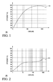
- FIG. 1 illustrates a graph 100 of the efficiency of a charge pump divider known in the prior art versus load current.
- the horizontal axis represents load current in milliAmperes (mA) using a logarithmic scale, and the vertical axis represents efficiency in percentage using a linear scale.
- a waveform 110 represents the efficiency of a typical charge pump converter using a divide-by-2 architecture versus load current.
- load currents such as 100 mA to over 1 A
- efficiency is relatively high, peaking at about 98% at around 400-500 mA.
- efficiency drops markedly, including about 91% at around 100 mA, about 85% at around 50 mA, and about 65% at around 20 mA.
- the charge pump divider is inefficient in systems that require low power modes. While the charge pump divider has a very high peak efficiency of about 98%, efficiency at low loads is poor.
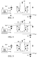
- FIG. 2 illustrates a graph 200 of the efficiency of an inductive buck converter known in the prior art versus load current.
- the horizontal axis represents load current in mA using a logarithmic scale, and the vertical axis represents efficiency in percentage using a linear scale.
- a waveform 210 represents the efficiency of a typical low voltage inductive buck converter. Efficiency peaks at about 91% at around 1 A, but only decreases slightly as the load decreases, including about 88% at around 100 mA, about 87% at about 10 mA, and about 80% at around 1 mA. While the inductive buck converter has fairly constant efficiency over a wide load range, its peak efficiency is low.
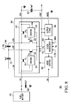
- FIG. 3 illustrates in partial block diagram and partial schematic form a charge pump divider 300 according to an embodiment of the present invention.
- Charge pump divider 300 includes generally an input capacitor 310, a capacitive divider core 320, a flying capacitor 330, an output capacitor 340, and a phase clock generator 350.
- Input capacitor 310 has a first terminal for receiving an input voltage labeled "V IN ", and a second terminal connected to ground.
- Capacitive divider core 320 includes N-channel metal oxide semiconductor (MOS) transistors 322, 324, 326, and 328.
- Transistor 322 has a drain for receiving V IN , a gate for receiving a signal labeled " ⁇ 1 ", and a source.
- MOS metal oxide semiconductor
- Transistor 324 has a drain connected to the source of transistor 322, a gate for receiving a signal labeled " ⁇ 2 ", and a source for providing a voltage labeled "V OUT ".
- Transistor 326 has a drain, a gate for receiving signal ⁇ 2 , and a source connected to ground.
- Transistor 328 has a drain connected to the source of transistor 324, a gate for receiving signal ⁇ 1 , and a source connected to the drain of transistor 326.
- Flying capacitor 330 has a first terminal connected to the source of transistor 322 and the drain of transistor 324, and a second terminal connected to the drain of transistor 326 and the source of transistor 328.
- Output capacitor 340 has a first terminal connected to the source of transistor 324 and to the drain of transistor 328, and a second terminal connected to ground.
- Phase clock generator 350 has a first output terminal for providing signal ⁇ 1 , and a second output terminal for providing signal ⁇ 2 .
- charge pump divider 300 is able to operate as a divide-by-two converter having both high peak efficiency and relatively constant efficiency over a wide load range by controlling the frequency of the generation of phase clock signals ⁇ 1 and ⁇ 2 .
- the basic operation of charge pump divider 300 will now be explained followed by a description of the operation of phase clock generator 350.
- FIG. 4 illustrates in partial block diagram and partial schematic form a diagram showing the operation of the charge pump divider of FIG. 3 during a first phase.
- the first phase corresponds signal ⁇ 1 being active at a logic high while signal ⁇ 2 is inactive at a logic low.
- transistors 322 and 328 are active and operate as closed switches, while transistors 324 and 326 are inactive and operate as open switches.
- the circuit path is shown by a dashed arrow 400. Neglecting the parasitic resistances of transistors 322 and 328, capacitors 330 and 340 are connected in series, and assuming they are equal-valued, V OUT will be about one-half of V IN .
- FIG. 5 illustrates in partial block diagram and partial schematic form a diagram showing the operation of charge pump divider 300 of FIG. 3 during a second phase.
- the second phase corresponds signal ⁇ 1 being inactive at a logic low while signal ⁇ 2 is active at a logic high.
- transistors 324 and 326 are active and operate as closed switches, while transistors 322 and 328 are inactive and operate as open switches.
- the circuit path is shown by a dashed arrow 500. Neglecting the parasitic resistances of transistors 324 and 326, capacitors 330 and 340 are connected in parallel between the node forming V OUT and ground.
- FIG. 6 illustrates a timing diagram 600 of voltages relevant to the operation of charge pump divider 300 of FIG. 3 .
- the horizontal axis represents time in microseconds ( ⁇ sec), while the vertical axis represents the amplitude of relevant signals in volts.
- Timing diagram 600 shows waveforms of two signals of interest, including a waveform 610 that represents the voltage across flying capacitor 330, and a waveform 620 that represents the voltage across output capacitor 340.
- input voltage V IN is assumed to be about 7.4 volts (V).
- waveform 610 the voltage across flying capacitor 330 has an average value of about 3.7 V but includes a ripple that causes it to vary between about 3.62 V and 3.78 V.
- the ripple across flying capacitor 330 is a triangular waveform at the switching frequency, and the average (DC) voltage is approximately equal to V IN /2.
- the ripple across output capacitor 340 is an asymmetric waveform at twice the switching frequency, and the average (DC) voltage depends on load current and in the illustrated example is about 3.6 V.
- FIG. 7 illustrates in block diagram form a frequency control circuit 700 for use in phase clock generator 350 of FIG. 3 .
- Frequency control circuit 700 includes a comparator 710, a switch 720, and an inverter 730.
- Comparator 710 has a positive input for receiving a voltage labeled "V_Cfly", a negative input, and an output for providing signal ⁇ 2 .
- Switch 720 has a first throw for receiving a first voltage labeled "V IN /2 - V P ", a second throw for receiving a second voltage labeled "V IN /2 + V P ", a common terminal connected to the negative input of comparator 710, and a control input connected to the output of comparator 710 for receiving the ⁇ 2 signal.
- Inverter 730 has an input connected to the output of comparator 710, and an output for providing the ⁇ 1 signal.
- Frequency control circuit 700 activates signal ⁇ 1 at a logic high and provides signal ⁇ 2 at a logic low when V_Cfly is less than V IN /2 - V P .
- switch 720 switches the V IN /2 + V P reference voltage to the negative input of comparator 710.
- flying capacitor 330 is connected in series with output capacitor 340 and the voltage across flying capacitor 330 increases.
- V_Cfly exceeds V IN /2 + V P
- frequency control circuit 700 activates signal ⁇ 2 at a logic high and provides signal ⁇ 1 at a logic low.
- switch 720 switches the V IN /2 - V P reference voltage to the negative input of comparator 710.
- phase flying capacitor 330 is connected in parallel with output capacitor 340 and the voltage across flying capacitor 330 decreases.
- frequency control circuit 700 again activates signal ⁇ 1 at a logic high and provides signal ⁇ 2 at a logic low, repeating the sequence.
- the switching frequency of the phase clock generator will adapt to the size of the load. Accordingly, for a higher load (larger slope of the ripple on V OUT ), the switching frequency increases and for a smaller load (smaller slope of the ripple on V OUT ), the switching frequency decreases.
- FIG. 8 illustrates in partial block diagram and partial schematic form a power converter 800 using an integrated circuit 860 based on charge pump divider 300 of FIG. 3 .
- Power converter 800 includes generally a two-cell battery 810, an input capacitor 820, a boost capacitor 830, a flying capacitor 840, and an output capacitor 850 all connected to an integrated circuit 860 in a manner that will be described as follows.
- Two-cell battery 810 has a positive output terminal connected to an integrated circuit terminal labeled "VIN”.
- Input capacitor 820 has a first terminal connected to the VIN terminal, and a second terminal connected to ground.
- Boost capacitor 830 has a first terminal connected to an integrated circuit terminal labeled "CB", and a second terminal connected to an integrated circuit terminal labeled "CPP".
- Flying capacitor 840 has a first terminal connected to the CPP terminal, and a second terminal connected to an integrated circuit terminal labeled "CPN".
- Output capacitor 850 has a first terminal connected to an integrated circuit terminal labeled "GND” that is connected to ground, and a second terminal connected to an integrated circuit terminal labeled "VOUT” that provides the output voltage.
- Integrated circuit 860 also has an enable terminal labeled "EN” for receiving an externally supplied enable signal, and an analog ground terminal labeled "AGND” connected to an analog ground voltage terminal.
- Integrated circuit 860 includes generally a capacitive divider core 870, a clock management block 880, a mode control block 890, and an output sense block 892.
- Capacitive divider core 870 includes transistors 322, 324, 326, and 328 labeled the same as corresponding elements in FIG. 3 and connected as described with respect to FIG. 3 .
- Capacitive divider core 860 has terminals connected to the VIN and GND terminals of integrated circuit 860, terminals connected to the CPP and CPN terminals for connection to external flying capacitor 840, a terminal connected to the CB terminal, input terminals for receiving the ⁇ 1 and ⁇ 2 clock signals, and an output terminal for providing an output voltage to the VOUT terminal.
- capacitive divider core 870 includes a set of drivers 872 for buffering clock signals ⁇ 1 and ⁇ 2 and providing similarly labeled buffered drive signals to the gates of transistors 322 and 324, respectively, and a set of drivers 874 for buffering clock signals ⁇ 1 and ⁇ 2 and providing similarly labeled buffered drive signals to the gates of transistors 328 and 326, respectively.
- Drivers 872 and 874 are used to buffer signals ⁇ 1 and ⁇ 2 from phase clock generator 880 to drive the gates of transistors 322, 324, 326, and 328, which are relatively large integrated MOS transistors with high gate capacitances.
- Integrated circuit 860 also includes additional features useful for forming a practical integrated circuit charge pump divider that can be adapted for different environments. For example, in order to raise the gate voltage of transistor 322 to a high enough level, a voltage greater than VIN is generated by means of the bootstrap capacitor connected between terminals CPP and CB. Integrated circuit 860 also includes a mode control block 890 used to enable the operation of capacitive divider core 870 or to place it in a low power mode based on the state of the EN terminal, and an output sense block 892 used for shutdown control in the case of an output fault. In addition, integrated circuit 860 includes circuitry that provides the V_CFLY, V P , and V IN /2 voltages to clock management circuit 880 that is not shown in FIG. 8 .
- FIG. 9 illustrates a graph of the relative efficiencies of the charge pump divider of FIG. 1 , the inductive buck converter of FIG. 2 , and the charge pump divider of FIG. 3 versus load current.
- the horizontal axis represents load current in mA using a logarithmic scale, and the vertical axis represents efficiency in percentage using a linear scale.
- a waveform 910 represents the efficiency of the known charge pump divider divider as previously shown in FIG. 1
- a waveform 920 represents the efficiency of the known inductive buck converter as shown in FIG. 2
- a waveform 930 represents the efficiency of charge pump divider 300 of FIG. 3 , all superimposed on common axes.
- charge pump divider 300 of FIG. 3 has about the same high peak efficiency as the capacitive divider of FIG. 1 , but also maintains near-peak efficiency over a wide load range similar to the inductive buck converter of FIG. 2 .
- charge pump divider 300 avoids the disadvantages of both architectures and is suitable for use in such applications as dual-cell portable devices that operate over very wide load ranges.
- the power converter built on the architecture of charge pump divider 300 of FIG. 3 is self-oscillating and the choice of a value for flying capacitor 330 will only affect the frequency and thus overall efficiency but not on the DC level and quality of VOUT. In some embodiments, it may be useful to limit the lower end of the self-oscillating frequency range to stay out of the audible frequency range, while degrading efficiency somewhat. In some embodiments, it is desirable to reduce electromagnetic interference (EMI) as well.
- EMI electromagnetic interference
- FIG. 10 illustrates in block diagram form a frequency spreading circuit 1000 that can be added to clock management block 880 of FIG. 8 to reduce EMI.
- Frequency spreading circuit 1000 includes a summing device 1010 and a noise source 1020.
- Summing device 1010 has a first input for receiving an input peak voltage labeled "V P "', a second input, and an output for providing signal V P .
- Noise source 1020 is connected to ground and has an output connected to the second input of summing device 1010 for providing a noise signal thereto.
- Noise source 1020 injects random noise having an average value of 0 V into the peak ripple voltage signal V P ' so that the output of summing device 1010 has an average value of V P ' but varies randomly within a range.
- Noise source 1020 varies the reference level of comparator 710, causing the actual switching frequency to vary. In this way, frequency spreading circuit 1000 introduces a jitter into the switching frequency of charge pump divider 300 to spread the emitted EMI over a frequency range proportional to the frequency range of the noise signal.
- the noise source may also be pseudo-random, produce shaped noise or a defined waveform shape.
- an integrated circuit charge pump divider can include different peripheral circuits to enable different operating modes, or remove certain features that are not needed for application-specific products.
- generation of the ⁇ 1 and ⁇ 2 signals could be accomplished using two comparators each receiving a fixed threshold rather than by shared comparator 710 used in frequency control circuit 700 of FIG. 2 .
- capacitive divider core 320 was shown as being constructed using only N-channel MOS transistors, in other embodiments it could also be formed with only P-channel transistors or with a combination of P-channel transistors and N-channel transistors.
- the substitution of a P-channel transistor for N-channel transistor 322 avoids the need for bootstrap capacitor 830, connected between terminals CB and CPP.
- input capacitor 820 can alternatively be connected between VIN and VOUT, which may improve the hot-plug robustness and may reduce output voltage ripple.
Landscapes
- Engineering & Computer Science (AREA)
- Physics & Mathematics (AREA)
- Electromagnetism (AREA)
- Power Engineering (AREA)
- General Physics & Mathematics (AREA)
- Radar, Positioning & Navigation (AREA)
- Automation & Control Theory (AREA)
- Dc-Dc Converters (AREA)
Abstract
Description
- The present disclosure relates generally to power conversion circuits, and more particularly to power converters using charge pump converters.
- Modern portable electronic products use to a wide extent rechargeable batteries to power internal circuitry. Smaller devices such as compact cameras, cellular telephones and phablets can use battery packs that are based on single-cell batteries that provide a direct current (DC) voltage over a range of, for example, 2.5 to 4.5 volts (V). In these devices the battery pack voltage can be used to drive an integrated circuit chipset directly. However larger mobile devices such as high-end digital still cameras, tablets and laptop computers require the use of battery packs with multiple battery cells for high current requirements. These cells can be configured in parallel, in series or "stacked", or as a combination of the two. The resulting battery packs generate a higher voltage in the range of, for example, 5V and 9V. The higher voltages are primarily used to power the larger displays, internal disk drivers, DVD drives, and the like. As a consequence however, in these larger devices, the chipset can no longer be powered directly from the battery pack and the higher battery voltage must to be reduced. Thus these devices typically use DC-DC buck converters to reduce the higher battery voltage to a level more suitable for powering integrated circuits.
- Moreover in order to preserve the limited battery life, these devices implement various screen-saving and power-saving modes. These different modes have caused the load conditions seen by the DC-DC converters (usually measured in terms of load current) to vary over a large range, possibly spanning up to three orders of magnitude or more. Because of the need to preserve battery life, the DC-DC converters need to be as efficient as possible under the widely varying load conditions.
- According to a first embodiment of the present invention there is provided a power converter using a charge pump divider comprising: a capacitive divider core having an input for receiving an input voltage and an output for providing an output voltage, wherein in a first phase said capacitive divider core is adapted to couple a flying capacitor in series with an output capacitor, and in a second phase said capacitive divider core is adapted to couple said flying capacitor in parallel with said output capacitor; and a phase clock generator that activates a first phase clock indicating said first phase when a flying voltage across said flying capacitor is less than a predetermined portion of said input voltage minus a peak voltage, and subsequently activates a second phase clock indicating said second phase when said flying voltage exceeds said predetermined portion of said input voltage plus said peak voltage.
- Preferably the power converter has said capacitive divider core comprising: a first switch having a first terminal for receiving said input voltage, a second terminal adapted to connect to a first terminal of said flying capacitor, and a control terminal for receiving said first phase clock; a second switch having a first terminal coupled to said second terminal of said first switch, a second terminal for providing said output voltage, and a control terminal for receiving said second phase clock; a third switch having a first terminal for receiving a reference voltage, a second terminal adapted to connect to a second terminal of said flying capacitor, and a control terminal for receiving said second phase clock; and a fourth switch having a first terminal coupled to said second terminal of said third switch, a second terminal coupled to said second terminal of said second switch, and a control terminal for receiving said first phase clock.
- Preferably the power converter includes said first, second, third, and fourth switches comprise N-channel MOS transistors.
- Preferably the power converter includes a flying capacitor having a value which is approximately equal to a value of said output capacitor, and said predetermined portion is equal to approximately one-half.
- Preferably the power converter said second phase clock is non-overlapping with respect to said first phase clock.
- More preferably, the power converter includes said phase clock generator comprises: a comparator having a positive input for receiving said flying voltage, a negative input, and an output for providing said second phase clock; a switch having a common terminal coupled to said negative input of said comparator, a first throw for receiving said predetermined portion of said input voltage plus said peak voltage, a second throw for receiving said predetermined portion of said input voltage minus said peak voltage, and a control terminal coupled to said output of said comparator; and an inverter having an input coupled to said output of said comparator, and an output for providing said first phase clock.
- More preferably the power converter further comprises: a summing device having a first input for receiving a predetermined voltage, a second input, and an output for providing said peak voltage; and a noise source having an output for providing a noise voltage that varies in an uncorrelated fashion with respect to said first phase clock and said second phase clock.
- More preferably the power converter comprises noise source comprises a random noise generator.
- More preferably the power converter comprises the power converter said noise source comprises a deterministic noise generator.
- More preferably the integrated circuit power converter using a charge pump divider further comprises: a first terminal adapted to receive an input voltage; a second terminal adapted to provide an output voltage; a third terminal adapted to be coupled to a reference voltage terminal; a fourth terminal adapted to be coupled to a first terminal of a flying capacitor; a fifth terminal adapted to be coupled to a second terminal of said flying capacitor; a capacitive divider core coupled to said first, second, third, fourth, and fifth terminals, wherein in a first phase said capacitive divider core is adapted to couple said first terminal to said fourth terminal and said fifth terminal to said second terminal, and during a second phase to couple said third terminal to said fifth terminal and said fourth terminal to said second terminal; and a phase clock generator for activating said capacitive divider core to operate in said first phase when a flying voltage between said fourth and fifth terminals is less than a predetermined portion of said input voltage minus a peak voltage, and subsequently activates said capacitive divider core to operate in said second phase when said flying voltage exceeds said predetermined portion of said input voltage plus said peak voltage.
- More preferably an embodiment of the invention includes an integrated circuit power converter using a power converter as described above, the integrated circuit power converter further comprising: a first terminal adapted to receive said input voltage; a second terminal adapted to provide said output voltage; a third terminal adapted to be coupled to a reference voltage terminal; a fourth terminal adapted to be coupled to a first terminal of said flying capacitor; and a fifth terminal adapted to be coupled to a second terminal of said flying capacitor, wherein said capacitive divider core is coupled to said first, second, third, fourth, and fifth terminals, wherein in said first phase said capacitive divider core is adapted to couple said first terminal to said fourth terminal and said fifth terminal to said second terminal, and during said second phase to couple said third terminal to said fifth terminal and said fourth terminal to said second terminal.
- Preferably the integrated circuit power converter includes said capacitive divider core comprises: a first switch having a first terminal for receiving said input voltage, a second terminal adapted to connect to a first terminal of said flying capacitor, and a control terminal for receiving a first phase clock indicative of said first phase; a second switch having a first terminal coupled to said second terminal of said first switch, a second terminal for providing said output voltage, and a control terminal for receiving a second phase clock indicative of said second phase; a third switch having a first terminal coupled to said reference voltage terminal, a second terminal adapted to connect to a second terminal of said flying capacitor, and a control terminal for receiving said second phase clock; and a fourth switch having a first terminal coupled to said second terminal of said third switch, a second terminal coupled to said second terminal of said second switch, and a control terminal for receiving said first phase clock.
- Preferably the integrated circuit power converter described above in which said first, second, third, and fourth switches comprise N-channel MOS transistors.
- Preferably the integrated circuit power converter described above and wherein said second terminal is further adapted to be coupled to a first terminal of an output capacitor, a size of said flying capacitor is approximately equal to a size of said output capacitor and said predetermined portion is equal to approximately one-half.
- Preferably the integrated circuit power converter described above wherein said second phase clock is non-overlapping with respect to said first phase clock.
- Preferably the integrated circuit power converter of
claim 10, wherein said phase clock generator comprises: a comparator having a positive input for receiving said flying voltage, a negative input, and an output for providing a second phase clock indicative of said second phase; a switch having a common terminal coupled to said negative input of said comparator, a first throw for receiving said predetermined portion of said input voltage plus said peak voltage, a second throw for receiving said predetermined portion of said input voltage minus said peak voltage, and a control terminal coupled to said output of said comparator; and an inverter having an input coupled to said output of said comparator, and an output for providing a first phase clock indicative of said first phase. - Preferably the integrated circuit power converter as described above, further comprising: a summing device having a first input for receiving a predetermined voltage, a second input, and an output for providing said peak voltage; and a noise source having an output for providing a noise voltage that varies in an uncorrelated fashion with respect to a first phase clock indicative of said first phase and a second phase clock indicative of said second phase.
- In another embodiment of the present invention there is provided a method comprising: receiving an input voltage on an input terminal; coupling a first terminal of a flying capacitor to said input terminal and a second terminal of said flying capacitor to a first terminal of an output capacitor during a first phase; coupling said second terminal of said flying capacitor to a voltage reference terminal and said first terminal of said flying capacitor to said first terminal of said output capacitor during a second phase; starting said first phase when a flying voltage across said flying capacitor is less than a predetermined portion of said input voltage minus a peak voltage; and ending said first phase and subsequently starting said second phase when said flying voltage exceeds said predetermined portion of said input voltage plus said peak voltage.
- Preferably the method, further comprises: repeating starting said first phase and subsequently starting said second phase continuously during a normal operation mode.
- Preferably the method, further comprises: adding a noise voltage to a predetermined voltage to obtain said peak voltage.
- Yet more preferably the method starting said first phase, and ending said first phase and subsequently starting said second phase further comprises: comparing said flying voltage to a second voltage; and generating said second voltage to alternately be approximately equal to said predetermined portion of said input voltage plus said peak voltage during said first phase, and said predetermined portion of said input voltage minus said peak voltage during said second phase.
- The present disclosure may be better understood, and its numerous features and advantages made apparent to those skilled in the art by referencing the accompanying drawings, in which:
-
FIG. 1 illustrates a graph of the efficiency of a capacitive divider known in the prior art versus load current; -
FIG. 2 illustrates a graph of the efficiency of an inductive buck converter known in the prior art versus load current; -
FIG. 3 illustrates in partial block diagram and partial schematic form a charge pump divider according to an embodiment of the present invention; -
FIG. 4 illustrates in partial block diagram and partial schematic form a diagram showing the operation of the charge pump divider ofFIG. 3 during a first phase; -
FIG. 5 illustrates in partial block diagram and partial schematic form a diagram showing the operation of the charge pump divider ofFIG. 3 during a second phase; -
FIG. 6 illustrates a timing diagram of voltages relevant to the operation of the charge pump divider ofFIG. 3 ; -
FIG. 7 illustrates in block diagram form a frequency control circuit for use in the phase clock generator ofFIG. 3 ; -
FIG. 8 illustrates in partial block diagram and partial schematic form a power converter using an integrated circuit based on the charge pump divider ofFIG. 3 ; and -
FIG. 9 illustrates a graph of the relative efficiencies of the charge pump divider ofFIG. 1 , the inductive buck converter ofFIG. 2 , and the charge pump divider ofFIG. 3 versus load current; and -
FIG. 10 illustrates in block diagram form a frequency spreading circuit that can be added to the clock management block ofFIG. 8 to reduce EMI. - The use of the same reference symbols in different drawings indicates similar or identical items. Unless otherwise noted, the word "coupled" and its associated verb forms include both direct connection and indirect electrical connection by means known in the art, and unless otherwise noted any description of direct connection implies alternate embodiments using suitable forms of indirect electrical connection as well.
-
FIG. 1 illustrates agraph 100 of the efficiency of a charge pump divider known in the prior art versus load current. InFIG. 1 the horizontal axis represents load current in milliAmperes (mA) using a logarithmic scale, and the vertical axis represents efficiency in percentage using a linear scale. Awaveform 110 represents the efficiency of a typical charge pump converter using a divide-by-2 architecture versus load current. At higher load currents, such as 100 mA to over 1 A, efficiency is relatively high, peaking at about 98% at around 400-500 mA. However as current decreases from the peak, efficiency drops markedly, including about 91% at around 100 mA, about 85% at around 50 mA, and about 65% at around 20 mA. Thus the charge pump divider is inefficient in systems that require low power modes. While the charge pump divider has a very high peak efficiency of about 98%, efficiency at low loads is poor. -
FIG. 2 illustrates agraph 200 of the efficiency of an inductive buck converter known in the prior art versus load current. InFIG. 2 the horizontal axis represents load current in mA using a logarithmic scale, and the vertical axis represents efficiency in percentage using a linear scale. Awaveform 210 represents the efficiency of a typical low voltage inductive buck converter. Efficiency peaks at about 91% at around 1 A, but only decreases slightly as the load decreases, including about 88% at around 100 mA, about 87% at about 10 mA, and about 80% at around 1 mA. While the inductive buck converter has fairly constant efficiency over a wide load range, its peak efficiency is low. -
FIG. 3 illustrates in partial block diagram and partial schematic form acharge pump divider 300 according to an embodiment of the present invention.Charge pump divider 300 includes generally aninput capacitor 310, acapacitive divider core 320, aflying capacitor 330, anoutput capacitor 340, and aphase clock generator 350.Input capacitor 310 has a first terminal for receiving an input voltage labeled "VIN", and a second terminal connected to ground.Capacitive divider core 320 includes N-channel metal oxide semiconductor (MOS)transistors Transistor 322 has a drain for receiving VIN, a gate for receiving a signal labeled "Φ1", and a source.Transistor 324 has a drain connected to the source oftransistor 322, a gate for receiving a signal labeled "Φ2", and a source for providing a voltage labeled "VOUT".Transistor 326 has a drain, a gate for receiving signal Φ2, and a source connected to ground.Transistor 328 has a drain connected to the source oftransistor 324, a gate for receiving signal Φ1, and a source connected to the drain oftransistor 326. Flyingcapacitor 330 has a first terminal connected to the source oftransistor 322 and the drain oftransistor 324, and a second terminal connected to the drain oftransistor 326 and the source oftransistor 328.Output capacitor 340 has a first terminal connected to the source oftransistor 324 and to the drain oftransistor 328, and a second terminal connected to ground.Phase clock generator 350 has a first output terminal for providing signal Φ1, and a second output terminal for providing signal Φ2. - As will now be explained,
charge pump divider 300 is able to operate as a divide-by-two converter having both high peak efficiency and relatively constant efficiency over a wide load range by controlling the frequency of the generation of phase clock signals Φ1 and Φ2. The basic operation ofcharge pump divider 300 will now be explained followed by a description of the operation ofphase clock generator 350. -
FIG. 4 illustrates in partial block diagram and partial schematic form a diagram showing the operation of the charge pump divider ofFIG. 3 during a first phase. The first phase corresponds signal Φ1 being active at a logic high while signal Φ2 is inactive at a logic low. During the first phase,transistors transistors arrow 400. Neglecting the parasitic resistances oftransistors capacitors -
FIG. 5 illustrates in partial block diagram and partial schematic form a diagram showing the operation ofcharge pump divider 300 ofFIG. 3 during a second phase. The second phase corresponds signal Φ1 being inactive at a logic low while signal Φ2 is active at a logic high. During the second phase,transistors transistors arrow 500. Neglecting the parasitic resistances oftransistors capacitors -
FIG. 6 illustrates a timing diagram 600 of voltages relevant to the operation ofcharge pump divider 300 ofFIG. 3 . InFIG. 6 , the horizontal axis represents time in microseconds (µsec), while the vertical axis represents the amplitude of relevant signals in volts. Timing diagram 600 shows waveforms of two signals of interest, including awaveform 610 that represents the voltage across flyingcapacitor 330, and awaveform 620 that represents the voltage acrossoutput capacitor 340. In timing diagram 600, input voltage VIN is assumed to be about 7.4 volts (V). Inwaveform 610, the voltage across flyingcapacitor 330 has an average value of about 3.7 V but includes a ripple that causes it to vary between about 3.62 V and 3.78 V. The ripple across flyingcapacitor 330 is a triangular waveform at the switching frequency, and the average (DC) voltage is approximately equal to VIN/2. Inwaveform 620, the ripple acrossoutput capacitor 340 is an asymmetric waveform at twice the switching frequency, and the average (DC) voltage depends on load current and in the illustrated example is about 3.6 V. - Since the output ripple of a fixed frequency charge pump increases with the load, the inventor has discovered that the efficiency of
charge pump 300 ofFIG. 3 can be improved by varying the switching frequency to obtain a constant peak-to-peak ripple. A circuit for use inphase clock generator 350 that varies the switching frequency to obtain a constant ripple will now be described. -
FIG. 7 illustrates in block diagram form afrequency control circuit 700 for use inphase clock generator 350 ofFIG. 3 .Frequency control circuit 700 includes acomparator 710, aswitch 720, and aninverter 730.Comparator 710 has a positive input for receiving a voltage labeled "V_Cfly", a negative input, and an output for providing signal Φ2.Switch 720 has a first throw for receiving a first voltage labeled "VIN/2 - VP", a second throw for receiving a second voltage labeled "VIN/2 + VP", a common terminal connected to the negative input ofcomparator 710, and a control input connected to the output ofcomparator 710 for receiving the Φ2 signal.Inverter 730 has an input connected to the output ofcomparator 710, and an output for providing the Φ1 signal. -
Frequency control circuit 700 activates signal Φ1 at a logic high and provides signal Φ2 at a logic low when V_Cfly is less than VIN/2 - VP. When signal Φ2 goes low,switch 720 switches the VIN/2 + VP reference voltage to the negative input ofcomparator 710. During thisphase flying capacitor 330 is connected in series withoutput capacitor 340 and the voltage across flyingcapacitor 330 increases. When V_Cfly exceeds VIN/2 + VP,frequency control circuit 700 activates signal Φ2 at a logic high and provides signal Φ1 at a logic low. When signal Φ2 goes high,switch 720 switches the VIN/2 - VP reference voltage to the negative input ofcomparator 710. During thisphase flying capacitor 330 is connected in parallel withoutput capacitor 340 and the voltage across flyingcapacitor 330 decreases. When V_Cfly is less than VIN/2 - VP,frequency control circuit 700 again activates signal Φ1 at a logic high and provides signal Φ2 at a logic low, repeating the sequence. In this manner, the switching frequency of the phase clock generator will adapt to the size of the load. Accordingly, for a higher load (larger slope of the ripple on VOUT), the switching frequency increases and for a smaller load (smaller slope of the ripple on VOUT), the switching frequency decreases. -
FIG. 8 illustrates in partial block diagram and partial schematic form apower converter 800 using anintegrated circuit 860 based oncharge pump divider 300 ofFIG. 3 .Power converter 800 includes generally a two-cell battery 810, aninput capacitor 820, aboost capacitor 830, a flyingcapacitor 840, and anoutput capacitor 850 all connected to anintegrated circuit 860 in a manner that will be described as follows. Two-cell battery 810 has a positive output terminal connected to an integrated circuit terminal labeled "VIN".Input capacitor 820 has a first terminal connected to the VIN terminal, and a second terminal connected to ground.Boost capacitor 830 has a first terminal connected to an integrated circuit terminal labeled "CB", and a second terminal connected to an integrated circuit terminal labeled "CPP". Flyingcapacitor 840 has a first terminal connected to the CPP terminal, and a second terminal connected to an integrated circuit terminal labeled "CPN".Output capacitor 850 has a first terminal connected to an integrated circuit terminal labeled "GND" that is connected to ground, and a second terminal connected to an integrated circuit terminal labeled "VOUT" that provides the output voltage.Integrated circuit 860 also has an enable terminal labeled "EN" for receiving an externally supplied enable signal, and an analog ground terminal labeled "AGND" connected to an analog ground voltage terminal. -
Integrated circuit 860 includes generally acapacitive divider core 870, aclock management block 880, amode control block 890, and anoutput sense block 892.Capacitive divider core 870 includestransistors FIG. 3 and connected as described with respect toFIG. 3 .Capacitive divider core 860 has terminals connected to the VIN and GND terminals ofintegrated circuit 860, terminals connected to the CPP and CPN terminals for connection toexternal flying capacitor 840, a terminal connected to the CB terminal, input terminals for receiving the Φ1 and Φ2 clock signals, and an output terminal for providing an output voltage to the VOUT terminal. In addition to the transistors described inFIG. 3 ,capacitive divider core 870 includes a set ofdrivers 872 for buffering clock signals Φ1 and Φ2 and providing similarly labeled buffered drive signals to the gates oftransistors drivers 874 for buffering clock signals Φ1 and Φ2 and providing similarly labeled buffered drive signals to the gates oftransistors Drivers phase clock generator 880 to drive the gates oftransistors -
Integrated circuit 860 also includes additional features useful for forming a practical integrated circuit charge pump divider that can be adapted for different environments. For example, in order to raise the gate voltage oftransistor 322 to a high enough level, a voltage greater than VIN is generated by means of the bootstrap capacitor connected between terminals CPP and CB.Integrated circuit 860 also includes a mode control block 890 used to enable the operation ofcapacitive divider core 870 or to place it in a low power mode based on the state of the EN terminal, and an output sense block 892 used for shutdown control in the case of an output fault. In addition, integratedcircuit 860 includes circuitry that provides the V_CFLY, VP, and VIN/2 voltages toclock management circuit 880 that is not shown inFIG. 8 . -
FIG. 9 illustrates a graph of the relative efficiencies of the charge pump divider ofFIG. 1 , the inductive buck converter ofFIG. 2 , and the charge pump divider ofFIG. 3 versus load current. InFIG. 9 the horizontal axis represents load current in mA using a logarithmic scale, and the vertical axis represents efficiency in percentage using a linear scale. Awaveform 910 represents the efficiency of the known charge pump divider divider as previously shown inFIG. 1 , awaveform 920 represents the efficiency of the known inductive buck converter as shown inFIG. 2 , and awaveform 930 represents the efficiency ofcharge pump divider 300 ofFIG. 3 , all superimposed on common axes. As can be readily seen fromFIG. 9 ,charge pump divider 300 ofFIG. 3 has about the same high peak efficiency as the capacitive divider ofFIG. 1 , but also maintains near-peak efficiency over a wide load range similar to the inductive buck converter ofFIG. 2 . Thuscharge pump divider 300 avoids the disadvantages of both architectures and is suitable for use in such applications as dual-cell portable devices that operate over very wide load ranges. - The power converter built on the architecture of
charge pump divider 300 ofFIG. 3 is self-oscillating and the choice of a value for flyingcapacitor 330 will only affect the frequency and thus overall efficiency but not on the DC level and quality of VOUT. In some embodiments, it may be useful to limit the lower end of the self-oscillating frequency range to stay out of the audible frequency range, while degrading efficiency somewhat. In some embodiments, it is desirable to reduce electromagnetic interference (EMI) as well. -
FIG. 10 illustrates in block diagram form afrequency spreading circuit 1000 that can be added toclock management block 880 ofFIG. 8 to reduce EMI.Frequency spreading circuit 1000 includes a summingdevice 1010 and anoise source 1020. Summingdevice 1010 has a first input for receiving an input peak voltage labeled "VP"', a second input, and an output for providing signal VP. Noise source 1020 is connected to ground and has an output connected to the second input of summingdevice 1010 for providing a noise signal thereto.Noise source 1020 injects random noise having an average value of 0 V into the peak ripple voltage signal VP' so that the output of summingdevice 1010 has an average value of VP' but varies randomly within a range.Noise source 1020 varies the reference level ofcomparator 710, causing the actual switching frequency to vary. In this way,frequency spreading circuit 1000 introduces a jitter into the switching frequency ofcharge pump divider 300 to spread the emitted EMI over a frequency range proportional to the frequency range of the noise signal. The noise source may also be pseudo-random, produce shaped noise or a defined waveform shape. - The above-disclosed subject matter is to be considered illustrative, and not restrictive, and the appended claims are intended to cover all such modifications, enhancements, and other embodiments that fall within the true scope of the claims. For example in other embodiments, an integrated circuit charge pump divider can include different peripheral circuits to enable different operating modes, or remove certain features that are not needed for application-specific products. Moreover the generation of the Φ1 and Φ2 signals could be accomplished using two comparators each receiving a fixed threshold rather than by shared
comparator 710 used infrequency control circuit 700 ofFIG. 2 . Also whilecapacitive divider core 320 was shown as being constructed using only N-channel MOS transistors, in other embodiments it could also be formed with only P-channel transistors or with a combination of P-channel transistors and N-channel transistors. The substitution of a P-channel transistor for N-channel transistor 322 avoids the need forbootstrap capacitor 830, connected between terminals CB and CPP. Moreoverinput capacitor 820 can alternatively be connected between VIN and VOUT, which may improve the hot-plug robustness and may reduce output voltage ripple. - Thus, to the maximum extent allowed by law, the scope of the present invention is to be determined by the broadest permissible interpretation of the following claims and their equivalents, and shall not be restricted or limited by the foregoing detailed description.
Claims (14)
- A power converter using a charge pump divider (300) comprising:a capacitive divider core (320) having an input for receiving an input voltage and an output for providing an output voltage, wherein in a first phase said capacitive divider core (320) is adapted to couple a flying capacitor (330) in series with an output capacitor (340), and in a second phase said capacitive divider core (320) is adapted to couple said flying capacitor (330) in parallel with said output capacitor (340); ana phase clock generator (350) that activates a first phase clock indicating said first phase when a flying voltage across said flying capacitor (330) is less than a predetermined portion of said input voltage minus a peak voltage, and subsequently activates a second phase clock indicating said second phase when said flying voltage exceeds said predetermined portion of said input voltage plus said peak voltage.
- The power converter (300) of claim 1, wherein said capacitive divider core (320) comprises:a first switch (322) having a first terminal for receiving said input voltage, a second terminal adapted to connect to a first terminal of said flying capacitor (330), and a control terminal for receiving said first phase clock;a second switch (324) having a first terminal coupled to said second terminal of said first switch (322), a second terminal for providing said output voltage, and a control terminal for receiving said second phase clock;a third switch (326) having a first terminal for receiving a reference voltage, a second terminal adapted to connect to a second terminal of said flying capacitor (330), and a control terminal for receiving said second phase clock; anda fourth switch (328) having a first terminal coupled to said second terminal of said third switch (326), a second terminal coupled to said second terminal of said second switch, and a control terminal for receiving said first phase clock.
- The power converter (300) of claim 2, wherein said first (322), second (324), third (326), and fourth (328) switches comprise N-channel MOS transistors.
- The power converter (300) of claim 2, wherein a value of said flying capacitor (330) is approximately equal to a value of said output capacitor (340), and said predetermined portion is equal to approximately one-half.
- The power converter (300) of claim 1, wherein said second phase clock is non-overlapping with respect to said first phase clock.
- The power converter (300) of claim 1, wherein said phase clock generator (350) comprises:a comparator (710) having a positive input for receiving said flying voltage, a negative input, and an output for providing said second phase clock;a switch (720) having a common terminal coupled to said negative input of said comparator (710), a first throw for receiving said predetermined portion of said input voltage plus said peak voltage, a second throw for receiving said predetermined portion of said input voltage minus said peak voltage, and a control terminal coupled to said output of said comparator (710); andan inverter (730) having an input coupled to said output of said comparator (710), and an output for providing said first phase clock.
- The power converter (300) of claim 1, further comprising:a summing device (1010) having a first input for receiving a predetermined voltage, a second input, and an output for providing said peak voltage; anda noise source (1020) having an output for providing a noise voltage that varies in an uncorrelated fashion with respect to said first phase clock and said second phase clock.
- The power converter (300) of claim 7, wherein said noise source (1020) comprises a random noise generator.
- The power converter (300) of claim 7, wherein said noise source (1020) comprises a deterministic noise generator.
- An integrated circuit power converter (860) using the power converter (300) of any of claims 1-9, the integrated circuit power converter (860) further comprising:a first terminal adapted to receive said input voltage;a second terminal adapted to provide said output voltage;a third terminal adapted to be coupled to a reference voltage terminal;a fourth terminal adapted to be coupled to a first terminal of said flying capacitor; anda fifth terminal adapted to be coupled to a second terminal of said flying capacitor,wherein said capacitive divider core (320/870) is coupled to said first, second, third, fourth, and fifth terminals, wherein in said first phase said capacitive divider core (320) is adapted to couple said first terminal to said fourth terminal and said fifth terminal to said second terminal, and during said second phase to couple said third terminal to said fifth terminal and said fourth terminal to said second terminal.
- A method comprising:receiving an input voltage on an input terminal;coupling a first terminal of a flying capacitor (330) to said input terminal and a second terminal of said flying capacitor (330) to a first terminal of an output capacitor (340) during a first phase;coupling said second terminal of said flying capacitor (330) to a voltage reference terminal and said first terminal of said flying capacitor (330) to said first terminal of said output capacitor (340) during a second phase;starting said first phase when a flying voltage across said flying capacitor (330) is less than a predetermined portion of said input voltage minus a peak voltage; andending said first phase and subsequently starting said second phase when said flying voltage exceeds said predetermined portion of said input voltage plus said peak voltage.
- The method of claim 11, further comprising:repeating starting said first phase and subsequently starting said second phase continuously during a normal operation mode.
- The method of claim 11, further comprising:adding a noise voltage to a predetermined voltage to obtain said peak voltage.
- The method of claim 11 wherein starting said first phase, and ending said first phase and subsequently starting said second phase comprise:comparing said flying voltage to a second voltage; andgenerating said second voltage to alternately be approximately equal to said predetermined portion of said input voltage plus said peak voltage during said first phase, and said predetermined portion of said input voltage minus said peak voltage during said second phase.
Applications Claiming Priority (1)
| Application Number | Priority Date | Filing Date | Title |
|---|---|---|---|
| US14/448,388 US20160033988A1 (en) | 2014-07-31 | 2014-07-31 | Power converter using charge pump divider and method therefor |
Publications (2)
| Publication Number | Publication Date |
|---|---|
| EP2991214A2 true EP2991214A2 (en) | 2016-03-02 |
| EP2991214A3 EP2991214A3 (en) | 2016-04-06 |
Family
ID=53765134
Family Applications (1)
| Application Number | Title | Priority Date | Filing Date |
|---|---|---|---|
| EP15179137.3A Withdrawn EP2991214A3 (en) | 2014-07-31 | 2015-07-30 | Power converter using charge pump divider and method therefor |
Country Status (3)
| Country | Link |
|---|---|
| US (1) | US20160033988A1 (en) |
| EP (1) | EP2991214A3 (en) |
| CN (1) | CN204794685U (en) |
Cited By (1)
| Publication number | Priority date | Publication date | Assignee | Title |
|---|---|---|---|---|
| EP3490127A1 (en) * | 2017-11-28 | 2019-05-29 | Oticon A/s | A switched capacitor voltage converter for a rechargeable battery in a hearing aid |
Families Citing this family (11)
| Publication number | Priority date | Publication date | Assignee | Title |
|---|---|---|---|---|
| JP6574743B2 (en) * | 2016-09-14 | 2019-09-11 | 株式会社東芝 | Power circuit |
| KR20180051441A (en) * | 2016-09-27 | 2018-05-16 | 선전 구딕스 테크놀로지 컴퍼니, 리미티드 | Fingerprint Recognition System |
| CN106787764B (en) * | 2017-01-24 | 2023-03-17 | 广州健特电子有限公司 | DC/DC device |
| WO2018227278A1 (en) | 2017-06-12 | 2018-12-20 | Gbatteries Energy Canada Inc. | Battery charging through multi-stage voltage conversion |
| EP3484034A1 (en) * | 2017-11-14 | 2019-05-15 | GN Hearing A/S | A switched capacitor dc-dc converter comprising external and internal flying capacitors |
| US10931147B2 (en) * | 2018-03-29 | 2021-02-23 | Nuvolta Technologies (Hefei) Co., Ltd. | Hybrid power converter |
| US11043899B2 (en) * | 2018-09-20 | 2021-06-22 | Samuel Dylan Webb | Zero inductor voltage converter topology with improved switch utilization |
| TWI730488B (en) * | 2019-11-01 | 2021-06-11 | 華碩電腦股份有限公司 | Voltage converter and operating method thereof |
| US10848059B1 (en) * | 2019-11-07 | 2020-11-24 | Micron Technology, Inc. | Systems and methods involving charge pumps coupled with external pump capacitors and other circuitry |
| CN112510996B (en) * | 2021-01-29 | 2021-04-30 | 上海灵动微电子股份有限公司 | Charge pump circuit and operation method thereof |
| US12267016B2 (en) * | 2022-02-22 | 2025-04-01 | Cirrus Logic Inc. | Power converters |
Family Cites Families (4)
| Publication number | Priority date | Publication date | Assignee | Title |
|---|---|---|---|---|
| US4581545A (en) * | 1983-10-04 | 1986-04-08 | At&T Technologies | Schmitt trigger circuit |
| US5479172A (en) * | 1994-02-10 | 1995-12-26 | Racom Systems, Inc. | Power supply and power enable circuit for an RF/ID transponder |
| US7764526B1 (en) * | 2006-10-18 | 2010-07-27 | Intersil Americas Inc. | Hysteretic mode controller for capacitor voltage divider |
| EP2744091A1 (en) * | 2012-12-17 | 2014-06-18 | Nxp B.V. | Limitation of inrush- and input peak-currents in switched capacitor DC/DC converters |
-
2014
- 2014-07-31 US US14/448,388 patent/US20160033988A1/en not_active Abandoned
-
2015
- 2015-07-20 CN CN201520526516.XU patent/CN204794685U/en not_active Expired - Fee Related
- 2015-07-30 EP EP15179137.3A patent/EP2991214A3/en not_active Withdrawn
Non-Patent Citations (1)
| Title |
|---|
| None |
Cited By (2)
| Publication number | Priority date | Publication date | Assignee | Title |
|---|---|---|---|---|
| EP3490127A1 (en) * | 2017-11-28 | 2019-05-29 | Oticon A/s | A switched capacitor voltage converter for a rechargeable battery in a hearing aid |
| US10879792B2 (en) | 2017-11-28 | 2020-12-29 | Oticon A/S | Switched capacitor voltage converter for a rechargeable battery in a hearing aid |
Also Published As
| Publication number | Publication date |
|---|---|
| CN204794685U (en) | 2015-11-18 |
| US20160033988A1 (en) | 2016-02-04 |
| EP2991214A3 (en) | 2016-04-06 |
Similar Documents
| Publication | Publication Date | Title |
|---|---|---|
| US20160033988A1 (en) | Power converter using charge pump divider and method therefor | |
| US10903742B2 (en) | Switched-capacitor converter circuit, charging control system, and control method | |
| CN102904440B (en) | Device and method for controlling a buck-boost converter | |
| US9444324B2 (en) | Synchronous DC-DC converter | |
| JP5591641B2 (en) | Charging circuit, control IC thereof, and electronic device using the same | |
| US20160056657A1 (en) | Charge and discharge management system and movable power source using the same | |
| US20090273955A1 (en) | Optimum structure for charge pump circuit with bipolar output | |
| US20170288440A1 (en) | Secondary control device and charging system having the same | |
| US9417642B2 (en) | Bootstrap DC-DC converter | |
| US8274269B2 (en) | Switching circuit and small-size high-efficiency DC-DC converter for portable devices including the same | |
| US9071128B2 (en) | DC-DC converter | |
| JP4101212B2 (en) | Power circuit | |
| CN103384072A (en) | Electronic device | |
| US10110121B2 (en) | Charge pump with a rapid-discharge path | |
| TWI518474B (en) | Adaptive charge pump, controlling method thereof, and electronic device | |
| US8553375B2 (en) | Intelligent soft start control to reduce electrostatic discharge clamp current spikes | |
| US8076968B1 (en) | Low-input-voltage charge pump | |
| JP2009106072A (en) | Overvoltage protection circuit and electronic apparatus using the same | |
| CN101567685B (en) | Charge pump | |
| EP2840694A1 (en) | Multiple level charge pump generating four voltages with four distinctive levels, and method for the same | |
| US20110317456A1 (en) | Optimum structure for charge pump circuit with bipolar output | |
| US8618846B2 (en) | Solid-state switch driving circuit for vehicle | |
| WO2023087221A1 (en) | Power supply circuit and electronic device | |
| JP6069700B2 (en) | Switching power supply circuit, electronic device, and semiconductor integrated circuit device | |
| KR101253216B1 (en) | Charge pump circuit |
Legal Events
| Date | Code | Title | Description |
|---|---|---|---|
| PUAI | Public reference made under article 153(3) epc to a published international application that has entered the european phase |
Free format text: ORIGINAL CODE: 0009012 |
|
| AK | Designated contracting states |
Kind code of ref document: A2 Designated state(s): AL AT BE BG CH CY CZ DE DK EE ES FI FR GB GR HR HU IE IS IT LI LT LU LV MC MK MT NL NO PL PT RO RS SE SI SK SM TR |
|
| AX | Request for extension of the european patent |
Extension state: BA ME |
|
| PUAL | Search report despatched |
Free format text: ORIGINAL CODE: 0009013 |
|
| AK | Designated contracting states |
Kind code of ref document: A3 Designated state(s): AL AT BE BG CH CY CZ DE DK EE ES FI FR GB GR HR HU IE IS IT LI LT LU LV MC MK MT NL NO PL PT RO RS SE SI SK SM TR |
|
| AX | Request for extension of the european patent |
Extension state: BA ME |
|
| RIC1 | Information provided on ipc code assigned before grant |
Ipc: H02M 1/44 20070101ALI20160229BHEP Ipc: G05F 5/00 20060101ALI20160229BHEP Ipc: H02M 3/07 20060101AFI20160229BHEP |
|
| STAA | Information on the status of an ep patent application or granted ep patent |
Free format text: STATUS: THE APPLICATION IS DEEMED TO BE WITHDRAWN |
|
| 18D | Application deemed to be withdrawn |
Effective date: 20161007 |