EP2990779B1 - Device for detecting analyzed object in specimen and method therefor - Google Patents
Device for detecting analyzed object in specimen and method therefor Download PDFInfo
- Publication number
- EP2990779B1 EP2990779B1 EP14788103.1A EP14788103A EP2990779B1 EP 2990779 B1 EP2990779 B1 EP 2990779B1 EP 14788103 A EP14788103 A EP 14788103A EP 2990779 B1 EP2990779 B1 EP 2990779B1
- Authority
- EP
- European Patent Office
- Prior art keywords
- area
- reaction
- test
- light
- light source
- Prior art date
- Legal status (The legal status is an assumption and is not a legal conclusion. Google has not performed a legal analysis and makes no representation as to the accuracy of the status listed.)
- Active
Links
Images





Classifications
-
- G—PHYSICS
- G01—MEASURING; TESTING
- G01N—INVESTIGATING OR ANALYSING MATERIALS BY DETERMINING THEIR CHEMICAL OR PHYSICAL PROPERTIES
- G01N21/00—Investigating or analysing materials by the use of optical means, i.e. using sub-millimetre waves, infrared, visible or ultraviolet light
- G01N21/75—Systems in which material is subjected to a chemical reaction, the progress or the result of the reaction being investigated
-
- G—PHYSICS
- G01—MEASURING; TESTING
- G01N—INVESTIGATING OR ANALYSING MATERIALS BY DETERMINING THEIR CHEMICAL OR PHYSICAL PROPERTIES
- G01N21/00—Investigating or analysing materials by the use of optical means, i.e. using sub-millimetre waves, infrared, visible or ultraviolet light
- G01N21/84—Systems specially adapted for particular applications
- G01N21/8483—Investigating reagent band
-
- G—PHYSICS
- G01—MEASURING; TESTING
- G01N—INVESTIGATING OR ANALYSING MATERIALS BY DETERMINING THEIR CHEMICAL OR PHYSICAL PROPERTIES
- G01N2201/00—Features of devices classified in G01N21/00
- G01N2201/06—Illumination; Optics
- G01N2201/062—LED's
-
- G—PHYSICS
- G01—MEASURING; TESTING
- G01N—INVESTIGATING OR ANALYSING MATERIALS BY DETERMINING THEIR CHEMICAL OR PHYSICAL PROPERTIES
- G01N33/00—Investigating or analysing materials by specific methods not covered by groups G01N1/00 - G01N31/00
- G01N33/48—Biological material, e.g. blood, urine; Haemocytometers
- G01N33/50—Chemical analysis of biological material, e.g. blood, urine; Testing involving biospecific ligand binding methods; Immunological testing
- G01N33/53—Immunoassay; Biospecific binding assay; Materials therefor
- G01N33/543—Immunoassay; Biospecific binding assay; Materials therefor with an insoluble carrier for immobilising immunochemicals
- G01N33/54366—Apparatus specially adapted for solid-phase testing
Definitions
- the present invention relates to a device and method for detecting analytes in samples.
- a material analysis by an optical method uses principles such as absorbance, fluorescence, phosphorescence, chemiluminescence, reflectance, turbidity, refraction, and scattering.
- labels such as radioactive materials, enzymes, fluorescent materials, chemiluminescent materials, gold nanoparticles, carbon black, latex particles, and quantum dots have been mostly used.
- Some cases of the optical reactions generated by the labels may be detected by human eyes.
- analytical apparatus have to be used for more quantitative result.
- signal strength is different depending on concentrations of the biomaterials. Most of the signals are measured by setting a background for noise. To enhance the accuracy, a signal-to-noise ratio needs to be efficiently measured.
- methods such as initial calibration before the reaction is generated and background calibration may be used alone or a combination thereof may be used.
- radioimmunoassay As an analytical method of biomaterials using the above-mentioned principles, there are radioimmunoassay, enzyme-linked immunosorbent assay, particle agglutination assay, chemiluminescent immunoassay, real-time polymerase chain reaction, flow cytometry, immunochromatography, etc. These methods are not limited to the analysis of materials but have been used for a disease test or diagnosis, or the like.
- the analytical method of biomaterials may largely be classified into homogeneous assay of performing reaction only in a solution phase and a heterogeneous assay of separating analytes or labels onto the solid phase.
- the solid phase used in the heterogeneous assay there are a plastic plate or microparticles of a polystyrene material, a nitrocellulose membrane, magnetic particles, a glass slide, etc.
- the immunochromatography measures a reaction by a scheme of developing the reaction using a porous membrane as the solid phase, the gold nanoparticles or the latex particles as the labels, etc., and accumulating the labels on a test line by an antigen-antibody reaction.
- the immunochromatography may have easy operability and easily observe the label visually in some cases, and therefore has been very variously used for self-testing of pregnancy or ovulation, drug-of-abuse test, hemoglobin A1c test, cardiovascular disease test, infectious disease test, etc.
- the immunochromatography includes a control area in which it is verified whether the reaction is correctly generated in addition to a test area in which the antigen-antibody reaction is tested.
- the reaction may be tested visually.
- the visual test may not obtain the quantitative results and the test results may differ by users. It is also possible to overlook abnormal reaction due to errors by a user or accurate measurement of the reaction time. Therefore, to meet a demand for an apparatus for analyzing them, various technologies and products have been developed.
- an apparatus and a method for capturing an image of a reaction device using an analytical apparatus including image devices such as a charge-coupled device (CCD) and a complementary metal-oxide-semiconductor (CMOS) and then analyzing a signal and noise.
- image devices such as a charge-coupled device (CCD) and a complementary metal-oxide-semiconductor (CMOS)
- CMOS complementary metal-oxide-semiconductor
- the scheme of scanning, by the light source and the light receiving unit, the reaction device may use one light source and one light receiving unit to reduce errors due to a deviation of the light source or the light receiving unit, but has a disadvantage in that it needs a driving apparatus for moving the reaction device or the optical unit, and therefore is hardly miniaturized and needs to calculate background noise based on a graph of the scanning of the reaction results, and therefore makes the process complicated and difficult.
- the scheme of scanning the reaction device while fixing the light source and the light receiving unit may be miniaturized and simplify the measurement, but has a disadvantage in that the light source and the light receiving unit capable of measuring the test area or the control area and the background noise may not be easily configured and the accurate test may be made only when deviations in components of the light source and the light receiving unit are solved.
- U.S. Patents Nos. 5,580,794 and 5,837, 546 describe a disposal analytical apparatus for detecting reaction on a strip using reflectance by the light-emitting diode (LED) light sources and a light receiving unit.
- LED light-emitting diode
- the patents do not disclose an optical arrangement and a method capable of measuring background noise and therefore cannot but calculate result values only by initial calibration.
- the above-mentioned Patents are likely to cause wrong results due to interfering materials in samples having the color such as hemoglobin or bilirubin, and may have a limited applicable range.
- U.S. Patent No. 6,235,241 discloses an analytical apparatus for detecting reaction on a strip using transmission measurement by the light-emitting diode (LED) light sources and the light receiving units but does not disclose a method for effectively calibrating the light sources and background noise and has a problem in that the analytical apparatus may not be applied to a printed circuit board (PCB) on a plane in the case of using the transmission measurement and therefore may be complicated.
- PCB printed circuit board
- U.S. Patent No. 7,317,532 and the corresponding application US 2010/172802 A1 disclose an optical arrangement for detecting reaction on a strip using reflectance by an LED light source and a light receiving unit. That is, the optical arrangement is configured in a scheme of illuminating light from the LED light source which is disposed in the middle among the three LED light sources arranged in a row to the background area between the control area and the test area and then detecting the illuminated light by two light receiving units for the control area and the test area and illuminating the light from the LED light sources for the control area and the test area to the strip to transfer the reflectance results to the light receiving unit and then calibrating and calculating the signal and the noise.
- the optical arrangement uses the light receiving unit of the control area and the test area instead of the light receiving unit for the background area and therefore has a limitation in the accurate calibration.
- a self-contained system uses light reflectivity to examine intensity of a dyed spot on a device membrane surrounded by background area to discern information about the specimen that produced the spot.
- a master clock alternatively drives one LED focussed upon the spot center, and then drives two LEDS focused on the background area.
- Light reflected from the spot and background is detected by preferably two photodetectors ("PDs") spaced-apart a multiple of 90° azimuthal, a configuration discovered to minimize the effects of uneven membrane topography upon light intensity measurements.
- the PD outputs are average-summed together and are input to a phase lock-in amplifier system that enhances detected signal/noise by measuring signal voltage without producing noise.
- the lock-in system simultaneously positively and negatively amplifies the average-summed PD outputs, which amplified signal is then switched in synchronism with the LED drive signals. Only in-phase signals occurring during the active LED drive signal portion are sampled, and signal components present in the average-summed together PD output are essentially doubled in effective amplitude, thereby enhancing signal to noise ratios.
- the output of the switch is lowpass filtered to recover a noise-free DC level proportional to detected light intensity. A readout of the DC level provides an accurate measurement of the spot intensity.
- the positions of the LED focal plane and the PD focal plane are reversed.
- U.S. Patent No. 7,499,170 discloses an analytical apparatus for detecting reaction using reflectance by setting a background area on a strip by one LED light source and two light receiving units but may detect a signal only in one test area without including the control area and therefore has a problem in that the apparatus may not be suitable for detection of test errors or various tests and may be applied to only one test area.
- the above-mentioned analytical apparatuses and analytical methods may not suitably reduce deviations by calibrating the light sources and the light receiving unit on the equivalent condition.
- the present inventors have been tried to develop a miniaturized analytical apparatus and an analytical method for measuring a signal of reaction generated in the device for analyzing or detecting analytes in samples by the scheme in which a light source unit and a light receiving unit are fixed.
- the present inventors investigated a method for effectively analyzing the test device spatially divided into the test area, the control area, and the background area to optically indicate the reaction by using an analytical apparatus in which n light sources and at least n + 1 light receiving units are constructed, thereby completing the present invention.
- An object of the present invention is to provide a device for detecting analytes in samples.
- Another object of the present invention is to provide a method for detecting analytes in samples.
- the present inventors have been tried to develop a miniaturized analytical apparatus and an analytical method for measuring a signal of reaction generated in the device for analyzing or detecting analytes in samples by a scheme in which a light source unit and a light receiving unit are fixed.
- the present inventors investigated a method for effectively analyzing the test device spatially divided into the test area, the control area, and the background area to optically indicate the reaction using an analytical apparatus in which n light source units and at least n + 1 light receiving units are constructed.
- the device includes the n light source units, the reaction strip including the test area, the control area, and the background area, and the at least n + 1 light receiving units.
- n may be an integer more than 1.
- the light source unit may include the light source generating light.
- the light source unit may include known various light sources. For example, a light emitting diode (LED) and a laser may be used as the light source.
- LED light emitting diode
- the test area includes a material reacting to the analytes present in the samples.
- the reaction to the analytes may include various kinds of reactions and according to one implementation example, the reaction to the analytes may be binding.
- the material reacting to the analytes in the test area may be a capture agent binding to the analytes.
- An example of the capture agent used in the present invention may be protein, nucleic acid, lipid, carbohydrate, vitamin, or drug or a conjugated material thereof.
- the capture agent may be immobilized in the test area, in which the immobilization may be made by a method such as adsorption, hydrophobic interaction, a hydrogen bond, ionic interaction, and/or a covalent bond.
- a detailed example of the capture agent used in the present invention may include an antibody, receptor, streptavidin (or avidin), aptamer, lectin, DNA, RNA, ligand, coenzyme, inorganic ion, cofactor, sugar, lipid, or substrate.
- the device according to the present invention may further include a detection agent binding to the analytes.
- the detection agent may be a detection antibody.
- the detection agent may be included in a conjugated pad.
- the detection agent when there are the analytes in the samples, the detection agent may be conjugated with a label which may generate an optical signal indicating the presence of the analytes.
- the label may include various labels known in the art and may include, for example, enzymes (for example, alkaline phosphatase, ⁇ - galactosidase, horseradish peroxidase, ⁇ - glucosidase and cytochrome P450), gold particles (for example, gold nanoparticles), silver particles (for example, silver nanoparticles), fluorescent materials [for example, fluorescein, fluorescein Isothiocyanate (FITC), rhodamine 6G, rhodamine B, 6-carboxy-tetramethyl-rhodamine (TAMRA), Cy- 3, Cy-5, Texas Red, Alexa Fluor, DAPI (4,6-diamidino-2-phenylindole), and Coumarin], latex particles containing fluorescent dye or
- enzymes
- the control area is an area in which it is confirmed whether the reaction is generated properly.
- the control area may be constructed variously. For example, when the analytes are detected by sandwich immunoassay, the control area may be constructed using an antibody having binding capacity to a labeled detection antibody (for example, gold nanoparticle-detection antibody conjugate). If the method of the present invention is performed using the device of the present invention regardless of whether there are the analytes in the samples, the reaction may be generated in the control area. If the reaction is not generated in the control area, the results in the test area may be determined as errors.
- a labeled detection antibody for example, gold nanoparticle-detection antibody conjugate
- the capture agent included in the control area may be a material binding to the detection agent.
- the capture agent may be an antibody having the binding capacity to the detection antibody.
- the background area according to the present invention may have the same environment as the background environment (that is, environment other than the material used for the reaction in the test area and the control area) of the test area and the control area.
- the background area may be formed on the white nitrocellulose membrane, which may be used as itself without any treatment or with special treatment for reducing non-specific reaction or solution development.
- the background area may use white color to minimize the light absorption.
- the present invention includes the reaction strip including the background area to which the light from the light source unit is illuminated, in which the test area and the background area are illuminated with the same one light and the control area and the background area are illuminated with the same one light to let the test area and the control area share the background area and the light illuminated to the test area and the background area and the light illuminated to the control area and the background area may be the same or different.
- the light illuminated to the test area and the background area and the light illuminated to the control area and the background area may be the same.
- the term "same light” has a meaning including light emitted from the one light source unit and light having the same optical characteristics (for example, wavelength).
- the reaction strip including the test area, the background area, and the control area may be made of various materials of a porous membrane such as nitrocellulose, cellulose paper, glass fiber, plastic, glass, etc.
- the flow and reaction of the samples and the detection agent in the reaction strip may be performed by various schemes such as chromatography, a capillary phenomenon, mixing by stirring, and diffusion.
- At least n + 1 light receiving units configuring the device of the present invention may detect the light reflected from the test area, the control area, and the background area of the reaction strip, respectively, and may be arranged for the test area, the control area, and the background area, respectively. That is, the light emitted from the test area, the control area, and the background area, respectively, may be detected by each of the light receiving units.
- the best feature of the present invention is that the n light source units and the at least n + 1 light receiving units are used. Due to the features of the configuration, the following various technical advantages are obtained.
- the photodiode, the phototransistor, and the photoresistor may be used as the light receiving unit.
- the device of the present invention may be constructed for multiplex detection in which the test areas are configured in plural. Meanwhile, for the description of the operation scheme of the present invention, if it is assumed that the present invention detects one kind of analytes, the reaction strip may include one test area, control area, and background area, respectively.
- the light sources may include a first light source unit and a second light source unit
- the light receiving unit may include a first light receiving unit, a second light receiving unit, and a third light receiving unit and the light from the first light source unit may illuminate the test area and the background area
- the light from the second light source unit may illuminate the background area and the control area
- the light reflected from the test area, the background area, and the control area may be detected by the first light receiving unit, the second light receiving unit, and the third receiving unit, respectively (see FIG. 1 ).
- the test area and the control area may share the background area, such that the background noise may be removed by calibration.
- the device of the present invention may be constructed well to detect the multiplex reaction in which the test areas are configured in plural.
- the test area, the background area, or the test area and the background area may be at least two. Even the device for the multiplex detection may be sufficiently performed using one control area.
- the calibrations for one of at least two test areas and the control area may share the reaction of the background area.
- the device of the present invention including the plurality of test areas may be manufactured by various schemes unless it deviates from the principle that it shares the background area (see FIGS. 3 and 4 ).
- the device of the present invention may be configured to include four light source units, two test areas, two background areas, one control area, and five light receiving units.
- the calibrations for the first test area and the second test area may share the reaction of the first background area and the calibrations for the second test area and the control area may share the reaction of the second background area.
- the device of the present invention illustrated in FIG. 4 may be configured to include three light source units, two test areas, one background area, one control area, and four light receiving units.
- the calibrations for the second test area and the control area may share the reaction of the background area.
- the device of the present invention may further include a processor calibrating values detected by the light receiving unit for the background area to be the same value by using the value (initial value) detected by the light receiving unit before the reaction is generated in the test area and the control area and obtaining a calibration value before the reaction of the test area and the control area by using the calibration value before the reaction of the background area and the values detected by the light receiving unit for the test area and the control area.
- the processor may additionally perform a process of obtaining a calibration value after the reaction of the test area and the control area by using the calibration value before the reaction of the background area or the calibration value after the reaction and the values detected after the reaction in the light receiving unit for the test area and the control area, after the reaction is generated in the test area and the control area.
- the processor may additionally perform a process of determining a value of an equation using the calibration value before the reaction and the calibration value after the reaction in the test area and the control area as a final measurement value of the test area and the control area.
- the equation used to obtain the final measurement value may be arbitrarily set.
- the processor may additionally perform a process of comparing the final measurement value with a predetermined cut-off value to qualitatively determine whether the analytes are present in the samples.
- the processor may additionally perform a process of substituting the final measurement value into a previously calculated quantification curve to quantitatively analyze the analytes in the samples.
- the device of the present invention may further include a microcontroller (for example, a central processing unit (CPU), a flash memory, an analog-to-digital converter (ADC), and a comparator), a voltage regulator, and/or a display (for example, LCD) for measurement control and calculation, in addition to the light source unit, the reaction strip, and the light receiving unit.
- a microcontroller for example, a central processing unit (CPU), a flash memory, an analog-to-digital converter (ADC), and a comparator
- ADC analog-to-digital converter
- a comparator for example, a voltage regulator
- a display for example, LCD
- the device of the present invention may further include a detector switch, a battery, and/or a serial programming connector.
- the present invention may be used to qualitatively or quantitatively detect the analytes.
- the present invention may be applied well for multiplex detection to detect the analytes in the samples.
- samples which may be used in the present invention may include blood, plasma, serum, urine, lymph, bone marrow, saliva, milk, ocular fluid, semen, brain extracts, spinal fluid, synovial fluid, thymic fluid, ascites, amniotic fluid, cell tissue liquid, buffer solution, tap water, polluted water, sewage, or ground water.
- the analytes to be analyzed may include proteins, peptides, nucleotide sequences, genes, lipids, carbohydrates, vitamins, drugs, organic compounds, inorganic matters, and liquefied gas but are not limited thereto.
- the present invention may be used in various fields such as diagnosis and prediction of disease, health care, paternity confirmation, physical constitution confirmation, fermentation engineering, biomedical engineering, food safety test, environmental analysis, cosmetics analysis and compound analysis.
- FIG. 1 is a diagram schematically illustrating a detailed implementation example of a device of the present invention.
- 1 Test area
- 3 Control area
- 4 Background area
- 10 Reaction strip
- 11 First light source unit
- 12 Second light source unit
- 21 First light receiving unit
- 24 Second light receiving unit
- 23 Third light receiving unit
- 31 Test line
- 33 Control line.
- FIG. 2 is a diagram schematically illustrating a device not covered by claim 1 of the present invention using an optical splitter.
- 1 Test area
- 3 Control area
- 4 Background area
- 10 Reaction strip
- 11 Light source unit
- 21 First light receiving unit
- 24 Second light receiving unit
- 23 Third light receiving unit
- 31 Test line
- 33 Control line
- 40 Optical splitter.
- FIG. 3 is a diagram schematically illustrating the implementation example of the device of the present invention having two test areas, two background areas, and one control area.
- 1 First test area
- 2 Second test area
- 3 Control area
- 5 First background area
- 4 Second background area
- 10 Reaction strip
- 11 First light source unit
- 12 Second light source unit
- 13 Third light source unit
- 14 Fourth light source unit
- 21 First light receiving unit
- 25 Second light receiving unit
- 23 Fifth light receiving unit
- 33 Control line.
- FIG. 4 is a diagram schematically illustrating the implementation example of the device of the present invention having two test areas, one background area, and one control area.
- 1 First test area
- 2 Second test area
- 3 Control area
- 4 Background area
- 10 Reaction strip
- 11 First light source unit
- 12 Second light source unit
- 13 Third light source unit
- 21 First light receiving unit
- 22 Second light receiving unit
- 24 Third light receiving unit
- 23 Fourth light receiving unit
- 33 Control line.
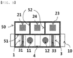
- FIG. 5 is a diagram schematically illustrating a detailed implementation example of an assembly of the device of the present invention, in which two light source units each are positioned thereover, corresponding to the test area and the control area.
- 10 Reaction strip
- 11 First light source unit
- 12 Second light source unit
- 21 First light receiving unit
- 24 Second light receiving unit
- 23 Third light receiving unit
- 31 Test line
- 33 Control line
- 50 Mechanism unit
- 51, 52 Barrier rib.
- FIG. 6 is a diagram schematically illustrating another implementation example of the assembly of the device of the present invention, in which three light source units each are positioned thereover, corresponding to the test area, the background area, and the control area.
- 10 Reaction strip
- 11 First light source unit
- 12 Second light source unit
- 21 First light receiving unit
- 24 Second light receiving unit
- 23 Third light receiving unit
- 31 Test line
- 33 Control line
- 50 Mechanism unit
- 51, 52 Barrier rib.
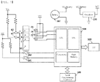
- FIG. 7 is a diagram schematically illustrating a configuration and a circuit according to the detailed implementation example of the device of the present invention.
- 61, 62 LED, 71, 73, 74: Phototransistor, 101: Detector switch, 102: Start switch, 103: Liquid crystal display (LCD), 106: Voltage regulator, 107: Coin battery, 108: Microcontroller, 109: Serial programming connector.
- LCD Liquid crystal display
- 106 Voltage regulator
- 107 Coin battery
- 108 Microcontroller
- 109 Serial programming connector.
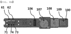
- FIGS. 8A and 8B are diagrams schematically illustrating a printed circuit board (PCB) according to the detailed implementation example of the device of the present invention, in which FIG. 8A illustrates that the LCD and the start switch are positioned at the upper portion of the PCB and FIG. 8B illustrates that the microcontroller, the battery, the light source unit, and the light receiving unit are positioned at the lower portion of the PCB.
- PCB printed circuit board
- FIG. 8A illustrates that the LCD and the start switch are positioned at the upper portion of the PCB
- FIG. 8B illustrates that the microcontroller, the battery, the light source unit, and the light receiving unit are positioned at the lower portion of the PCB.
- 102 Start switch
- 103 Liquid crystal display (LCD)
- 106 Voltage regulator
- 107 Coin battery
- 108 Microcontroller
- 109 Serial programming connector.
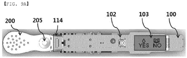
- FIGS. 9A and 9B are diagrams illustrating an upper portion and a lower portion of the PCB having a form in which a reaction strip housing according to the detailed implementation example of the device of the present invention is inserted into a mechanism unit, in which the mechanism unit is positioned at the lower portion of the PCB.
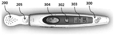
- FIG. 10A is a diagram schematically illustrating the reaction strip housing according to the detailed implementation example of the device of the present invention and FIG. 10B is a diagram schematically illustrating a measuring device into which the strip housing is inserted.
- 200 Reaction strip housing
- 201 Test line
- 203 Background area
- 204 Control line
- 205 Sample loading unit
- 300 Measurement device housing
- 302 Start button
- 303 LCD
- 304 Eject button.
- a detailed exemplary embodiment of the present invention is as follows.
- the best feature of the present invention is that light receiving units 21, 22, 23, 24, and 25 are arranged to be at least one more than light source units 11, 12, 13, and 14. That is, if n light source units 11, 12, 13, and 14 are used, the light receiving units 21, 22, 23, 24, and 25 are configured of at least n + 1. According to a configuration scheme of a device of the present invention, light from one light source unit is illuminated to a test area and a background area or a control area and a background area ( FIGS. 1 and 3 ) or two test areas ( FIG. 4 ) under the equivalent condition.
- the light receiving units 21, 22, 23, 24, and 25 need to be arranged to one to one correspond to the test areas 1 and 2 and the control area 3 so as to detect an optical reaction to the illuminated light and need to be arranged to one to one correspond to at least one background area 4 and 5.
- the test areas 1 and 2, the control area 3, and the background areas 4 and 5 of the device may be standardized by initial calibration of n light source units 11, 12, 13, and 14 and at least n + 1 light receiving units 21, 22, 23, 24, and 25. That is, if light from the light source in the device before the reaction is generated is illuminated to a combination of the test areas 1 and 2, the control area 3, and the background areas 4 and 5 under the equivalent conditions, the light receiving units 21, 22, 23, 24, and 25 one to one corresponding to each area detect light. In this case, two areas are illuminated with light from one light source under the equivalent conditions and each of the light source units 11, 12, 13, and 14 shares a common area, such that the standardization may be made.
- FIG. 1 illustrates an example of the analytical method.
- the two light source units 11 and 12 illuminate light to the test area 1, the control area 3, and the background area 4 on an immunochromatography strip 10 configured of one test line 31 and one control line 33 under the equivalent condition and thus the reflected light is detected by three light receiving units 21, 23, and 24.
- the first light source unit 11 illuminates light to the test area 1 and the background area 4 and thus the reflected light is detected by the first light receiving unit 21 for the test area 1 and the second light receiving area 24 for the background area 4.
- the second light source unit 12 illuminates light to the control area 3 and the background area 4 and thus the reflected light is detected by the second light receiving unit 23 and the third light receiving unit 24.
- FIG. 7 is a diagram schematically illustrating a configuration and a circuit of the device using the light source unit and the light receiving unit, according to the detailed implementation example of the device of the present invention
- FIGS. 8A and 8B are diagrams schematically illustrating an upper portion and a lower portion of a printed circuit board (PCB) according to the detailed implementation example of the device of the present invention
- FIGS. 9A and 9B are diagrams schematically illustrating the PCB having a form in which a reaction strip housing according to the detailed implementation example of the device of the present invention is inserted into a mechanism unit
- FIGS. 10A and 10B are diagrams schematically illustrating the reaction strip housing according to the detailed implementation example of the device of the present invention and a measurement device into which the strip housing is inserted.
- components such as light source units 61 and 62, light receiving units 71, 73, and 74, a microcontroller 108, a battery 107, an LCD 103, and switches 101 and 103 are positioned on a PCB 100.
- Various kinds of light source units such as red, green, blue, or three colors may be used and according to the detailed implementation example of the present invention, a green light-emitting diode (LED) is used.
- a phototransistor or a photodiode may be used and according to the detailed implementation example of the present invention, the phototransistor is used.
- the microcontroller may be implemented at low power and is configured to include a central processing unit (CPU) for calculation, an analog-to-digital converter (ADC), an analog comparator, a flash memory, an LCD driver, a serial communication interface, etc.
- CPU central processing unit
- ADC analog-to-digital converter
- a voltage is constantly maintained using a voltage regulator 106, thereby obtaining more stable results.
- a reaction device 200 if a reaction device 200 is inserted into a measurement device, a circuit is connected by the detector switch 101 and thus power is supplied from battery 107, thereby turning on the LCD 103.
- the LCD may be configured using various characters or diagrams and may display a progress of test and result errors. If power is supplied by a tact switch, an operation of the light source unit and the light receiving unit may be applied by various methods and according to the detailed implementation example of the present invention, after a start button 302 is pressed to turn on the start switch 103, the light source unit and the light receiving unit are operated. According to the detailed implementation example of the present invention, it may be connected to external devices such as a computer through the serial programming connector 109 to analyze the reaction. The test device performing the measurement is separated by pressing a ejecting button 304.
- a device strip before the reaction is generated is a white nitrocellulose membrane and is illuminated with light rays under the equivalent conditions, and light from the first light source unit 11 and the second light source unit 12 are illuminated to the common background area 4 and therefore two measurement values may be standardized by several schemes.
- the standardization scheme is applied to the control area 3 and thus values for the first light receiving unit 21 and the third light receiving unit 23 may also be standardized, such that although each of the light sources and the light receiving units uses separate components, all of them may be standardized before the reaction to perform the initial calibration.
- a test line 31 of the test area 1 defines signal strength by a label and a control line 33 t appears a signal by the label when the reaction is performed normally.
- the strip after the reaction is generated is not in an equivalent state and values measured after the reaction from the initial calibration measured before the reaction may be quantified by several schemes.
- the measurement values obtained by the device of FIG. 1 are defined and then the initial calibration, the background calibration, etc., may be performed as follows.
- [Table 1] Light source Light recei ving unit Measurement value of light receiving unit before reaction Measurement value of light receiving unit after reaction Before calibration After calibration Before calibration After calibration 11 21 T 0 T' 0 T t T' t 11 24 BT 0 BT' 0 BT t BT' t 12 23 C 0 C' 0 C t C' t 12 24 BC 0 BC' 0 BC t BC' t
- the measurement values obtained by the device of FIG. 1 are defined and then the initial calibration, the background calibration, etc., may be performed as follows.
- the calculated measurement values may be used for qualitative analysis depending on a predetermined cutoff value or are substituted into the a previously calculated quantitative curve, thereby calculating a quantitative value.
- the measured value in the control area may be used to verify the reaction or analyze a prozone phenomenon and may be used to input a specific value to reduce a deviation in the reaction strip and then calibrate the value of the test area depending on the input value.
- each measurement value is calibrated, the results may be determined without predetermined cutoff using a relative color intensity difference between the control line and the test line. That is, by a scheme of comparing the final measurement value TI of the test area 1 and the final measurement value CI of the control area 3, the cutoff is not predetermined and is set at a ratio of CI value. For example, if the cutoff is set to be 90% of CI, the reaction may be set to be determined as a positive when the TI is over the cutoff and the reaction may be set to be determined as a negative when the TI is under the cutoff.
- control area, the test area, and the background area are illuminated with light under the equivalent conditions and the light receiving units need to correspond to each area and the light receiving unit needs to be always arranged to be one more than the light source.
- the device configured of at least two test areas illustrated in FIGS. 3 and 4 may accurately measure the analytes by calibration.
Landscapes
- Life Sciences & Earth Sciences (AREA)
- Health & Medical Sciences (AREA)
- Chemical & Material Sciences (AREA)
- Physics & Mathematics (AREA)
- Biochemistry (AREA)
- Analytical Chemistry (AREA)
- General Health & Medical Sciences (AREA)
- General Physics & Mathematics (AREA)
- Immunology (AREA)
- Pathology (AREA)
- Molecular Biology (AREA)
- Engineering & Computer Science (AREA)
- Chemical Kinetics & Catalysis (AREA)
- Plasma & Fusion (AREA)
- Investigating Or Analysing Materials By The Use Of Chemical Reactions (AREA)
Description
- The present invention relates to a device and method for detecting analytes in samples.
- A material analysis by an optical method uses principles such as absorbance, fluorescence, phosphorescence, chemiluminescence, reflectance, turbidity, refraction, and scattering. To analyze biomaterials using the optical principles, labels such as radioactive materials, enzymes, fluorescent materials, chemiluminescent materials, gold nanoparticles, carbon black, latex particles, and quantum dots have been mostly used. Some cases of the optical reactions generated by the labels may be detected by human eyes. However analytical apparatus have to be used for more quantitative result. Upon the optical measurement of the biomaterials, signal strength is different depending on concentrations of the biomaterials. Most of the signals are measured by setting a background for noise. To enhance the accuracy, a signal-to-noise ratio needs to be efficiently measured. To measure the signal-to-noise ratio, generally, methods such as initial calibration before the reaction is generated and background calibration may be used alone or a combination thereof may be used.
- As an analytical method of biomaterials using the above-mentioned principles, there are radioimmunoassay, enzyme-linked immunosorbent assay, particle agglutination assay, chemiluminescent immunoassay, real-time polymerase chain reaction, flow cytometry, immunochromatography, etc. These methods are not limited to the analysis of materials but have been used for a disease test or diagnosis, or the like. The analytical method of biomaterials may largely be classified into homogeneous assay of performing reaction only in a solution phase and a heterogeneous assay of separating analytes or labels onto the solid phase. As the solid phase used in the heterogeneous assay, there are a plastic plate or microparticles of a polystyrene material, a nitrocellulose membrane, magnetic particles, a glass slide, etc.
- The immunochromatography measures a reaction by a scheme of developing the reaction using a porous membrane as the solid phase, the gold nanoparticles or the latex particles as the labels, etc., and accumulating the labels on a test line by an antigen-antibody reaction. The immunochromatography may have easy operability and easily observe the label visually in some cases, and therefore has been very variously used for self-testing of pregnancy or ovulation, drug-of-abuse test, hemoglobin A1c test, cardiovascular disease test, infectious disease test, etc. The immunochromatography includes a control area in which it is verified whether the reaction is correctly generated in addition to a test area in which the antigen-antibody reaction is tested. If the amount of samples is small or the reaction is not generated properly, a signal may not appear in the control area and if the concentrations of the analytes in the samples are high, the signal may be reduced or may not appear in the control area due to a prozone phenomenon. Technologies related to the immunochromatography have been known in several documents such as
U.S. Patents Nos. 5,073,484 ,5,591,645 ,5,559,041 , and6,485,982 . In addition to the immunochromatography using the porous membrane, the microfluidics for performing micromachining on a plastic surface to make a predetermined structure in which a solution may move by a capillary action is also used as a point-of care testing. The relevant example has been described in several documents such asU.S. Patents Nos. 6,767,510 and8,025,854 . - Meanwhile, when the gold nanoparticles, the colored latex particles, or the like are used as the labels, the reaction may be tested visually. However, the visual test may not obtain the quantitative results and the test results may differ by users. It is also possible to overlook abnormal reaction due to errors by a user or accurate measurement of the reaction time. Therefore, to meet a demand for an apparatus for analyzing them, various technologies and products have been developed.
- As the analytical apparatus and the analytical method, there are an apparatus and a method for capturing an image of a reaction device using an analytical apparatus including image devices such as a charge-coupled device (CCD) and a complementary metal-oxide-semiconductor (CMOS) and then analyzing a signal and noise. Currently, many products using the analytical apparatus and the analytical method have been commercialized. However, the analytical apparatus and the analytical method are hardly miniaturized because the reaction device and an imaging device need to be spaced apart from each other at a predetermined distance to secure good image quality, need to use an image device and expensive components consuming relatively larger power for image analysis.
- As another example, there are an analytical apparatus and an analytical method for measuring a signal and noise using a scheme of scanning the reaction device while moving a light source and a light receiving unit(photodetector) or a scheme of scanning the reaction device while fixing a light source and a light receiving unit, upon measuring the reaction in the reaction device. The scheme of scanning, by the light source and the light receiving unit, the reaction device may use one light source and one light receiving unit to reduce errors due to a deviation of the light source or the light receiving unit, but has a disadvantage in that it needs a driving apparatus for moving the reaction device or the optical unit, and therefore is hardly miniaturized and needs to calculate background noise based on a graph of the scanning of the reaction results, and therefore makes the process complicated and difficult. On the other hand, the scheme of scanning the reaction device while fixing the light source and the light receiving unit may be miniaturized and simplify the measurement, but has a disadvantage in that the light source and the light receiving unit capable of measuring the test area or the control area and the background noise may not be easily configured and the accurate test may be made only when deviations in components of the light source and the light receiving unit are solved.
-
U.S. Patents Nos. 5,580,794 and5,837, 546 describe a disposal analytical apparatus for detecting reaction on a strip using reflectance by the light-emitting diode (LED) light sources and a light receiving unit. However, the patents do not disclose an optical arrangement and a method capable of measuring background noise and therefore cannot but calculate result values only by initial calibration. In this case, the above-mentioned Patents are likely to cause wrong results due to interfering materials in samples having the color such as hemoglobin or bilirubin, and may have a limited applicable range. -
U.S. Patent No. 6,235,241 discloses an analytical apparatus for detecting reaction on a strip using transmission measurement by the light-emitting diode (LED) light sources and the light receiving units but does not disclose a method for effectively calibrating the light sources and background noise and has a problem in that the analytical apparatus may not be applied to a printed circuit board (PCB) on a plane in the case of using the transmission measurement and therefore may be complicated. -
U.S. Patent No. 7,317,532 and the corresponding applicationUS 2010/172802 A1 disclose an optical arrangement for detecting reaction on a strip using reflectance by an LED light source and a light receiving unit. That is, the optical arrangement is configured in a scheme of illuminating light from the LED light source which is disposed in the middle among the three LED light sources arranged in a row to the background area between the control area and the test area and then detecting the illuminated light by two light receiving units for the control area and the test area and illuminating the light from the LED light sources for the control area and the test area to the strip to transfer the reflectance results to the light receiving unit and then calibrating and calculating the signal and the noise. However, the optical arrangement uses the light receiving unit of the control area and the test area instead of the light receiving unit for the background area and therefore has a limitation in the accurate calibration. -
US 2004/071331 A1 A self-contained system uses light reflectivity to examine intensity of a dyed spot on a device membrane surrounded by background area to discern information about the specimen that produced the spot. In a preferred embodiment, a master clock alternatively drives one LED focussed upon the spot center, and then drives two LEDS focused on the background area. Light reflected from the spot and background is detected by preferably two photodetectors ("PDs") spaced-apart a multiple of 90° azimuthal, a configuration discovered to minimize the effects of uneven membrane topography upon light intensity measurements. The PD outputs are average-summed together and are input to a phase lock-in amplifier system that enhances detected signal/noise by measuring signal voltage without producing noise. The lock-in system simultaneously positively and negatively amplifies the average-summed PD outputs, which amplified signal is then switched in synchronism with the LED drive signals. Only in-phase signals occurring during the active LED drive signal portion are sampled, and signal components present in the average-summed together PD output are essentially doubled in effective amplitude, thereby enhancing signal to noise ratios. The output of the switch is lowpass filtered to recover a noise-free DC level proportional to detected light intensity. A readout of the DC level provides an accurate measurement of the spot intensity. In an embodiment, the positions of the LED focal plane and the PD focal plane are reversed. -
U.S. Patent No. 7,499,170 discloses an analytical apparatus for detecting reaction using reflectance by setting a background area on a strip by one LED light source and two light receiving units but may detect a signal only in one test area without including the control area and therefore has a problem in that the apparatus may not be suitable for detection of test errors or various tests and may be applied to only one test area. - In addition, the above-mentioned analytical apparatuses and analytical methods may not suitably reduce deviations by calibrating the light sources and the light receiving unit on the equivalent condition.
- Throughout the present specification, a number of articles and patent documents are referenced and the citation thereof is disclosed. The disclosure of the cited articles and patent documents is disclosed in the present specification as a whole and thus a level of the technical field to which the present invention belongs and the contents of the present invention will be more clearly described.
- The present inventors have been tried to develop a miniaturized analytical apparatus and an analytical method for measuring a signal of reaction generated in the device for analyzing or detecting analytes in samples by the scheme in which a light source unit and a light receiving unit are fixed. As a result, the present inventors investigated a method for effectively analyzing the test device spatially divided into the test area, the control area, and the background area to optically indicate the reaction by using an analytical apparatus in which n light sources and at least n + 1 light receiving units are constructed, thereby completing the present invention.
- An object of the present invention is to provide a device for detecting analytes in samples.
- Further, another object of the present invention is to provide a method for detecting analytes in samples.
- Other objects and advantages of the present invention will be more clearly described below with reference to the detailed description, claims, and drawings of the present invention.
- These objects of the present invention are solved by a device for detecting analytes in samples according to
claim 1 and a method for detecting analytes in samples according toclaim 12. - The present inventors have been tried to develop a miniaturized analytical apparatus and an analytical method for measuring a signal of reaction generated in the device for analyzing or detecting analytes in samples by a scheme in which a light source unit and a light receiving unit are fixed. As a result, the present inventors investigated a method for effectively analyzing the test device spatially divided into the test area, the control area, and the background area to optically indicate the reaction using an analytical apparatus in which n light source units and at least n + 1 light receiving units are constructed.
- The device according to the present invention includes the n light source units, the reaction strip including the test area, the control area, and the background area, and the at least n + 1 light receiving units. n may be an integer more than 1.
- The light source unit may include the light source generating light. According to the exemplary embodiment of the present invention, the light source unit may include known various light sources. For example, a light emitting diode (LED) and a laser may be used as the light source.
- According to the present invention, the test area includes a material reacting to the analytes present in the samples. The reaction to the analytes may include various kinds of reactions and according to one implementation example, the reaction to the analytes may be binding.
- According to one implementation example of the present invention, the material reacting to the analytes in the test area may be a capture agent binding to the analytes. An example of the capture agent used in the present invention may be protein, nucleic acid, lipid, carbohydrate, vitamin, or drug or a conjugated material thereof. According to one implementation example, the capture agent may be immobilized in the test area, in which the immobilization may be made by a method such as adsorption, hydrophobic interaction, a hydrogen bond, ionic interaction, and/or a covalent bond.
- A detailed example of the capture agent used in the present invention may include an antibody, receptor, streptavidin (or avidin), aptamer, lectin, DNA, RNA, ligand, coenzyme, inorganic ion, cofactor, sugar, lipid, or substrate.
- According to one implementation example of the present invention, when the material reacting to the analytes included in the test area is the capture agent, the device according to the present invention may further include a detection agent binding to the analytes. For example, when the capture agent is a capture antibody, the detection agent may be a detection antibody. In a rapid test kit using immunochromatography, the detection agent may be included in a conjugated pad.
- According to one implementation example of the present invention, when there are the analytes in the samples, the detection agent may be conjugated with a label which may generate an optical signal indicating the presence of the analytes. The label may include various labels known in the art and may include, for example, enzymes (for example, alkaline phosphatase, β - galactosidase, horseradish peroxidase, β - glucosidase and cytochrome P450), gold particles (for example, gold nanoparticles), silver particles (for example, silver nanoparticles), fluorescent materials [for example, fluorescein, fluorescein Isothiocyanate (FITC), rhodamine 6G, rhodamine B, 6-carboxy-tetramethyl-rhodamine (TAMRA), Cy- 3, Cy-5, Texas Red, Alexa Fluor, DAPI (4,6-diamidino-2-phenylindole), and Coumarin], latex particles containing fluorescent dye or pigment, chemiluminescent materials and coloring matters (for example, gardenia dye, eosin, phenol red, bromophenol blue, m-cresol purple, and bromocresol purple).
- According to the present invention, the control area is an area in which it is confirmed whether the reaction is generated properly. The control area may be constructed variously. For example, when the analytes are detected by sandwich immunoassay, the control area may be constructed using an antibody having binding capacity to a labeled detection antibody (for example, gold nanoparticle-detection antibody conjugate). If the method of the present invention is performed using the device of the present invention regardless of whether there are the analytes in the samples, the reaction may be generated in the control area. If the reaction is not generated in the control area, the results in the test area may be determined as errors.
- When the present invention uses the detection agent, the capture agent included in the control area may be a material binding to the detection agent. For example, when the detection agent is the detection antibody, the capture agent may be an antibody having the binding capacity to the detection antibody.
- According to one implementation example of the present invention, the background area according to the present invention may have the same environment as the background environment (that is, environment other than the material used for the reaction in the test area and the control area) of the test area and the control area. For example, when the test area and the control area are formed on a white nitrocellulose membrane, the background area may be formed on the white nitrocellulose membrane, which may be used as itself without any treatment or with special treatment for reducing non-specific reaction or solution development. According to the detailed exemplary embodiment of the present invention, the background area may use white color to minimize the light absorption.
- The present invention includes the reaction strip including the background area to which the light from the light source unit is illuminated, in which the test area and the background area are illuminated with the same one light and the control area and the background area are illuminated with the same one light to let the test area and the control area share the background area and the light illuminated to the test area and the background area and the light illuminated to the control area and the background area may be the same or different.
- According to an exemplary embodiment of the present invention, the light illuminated to the test area and the background area and the light illuminated to the control area and the background area may be the same. In the present specification, the term "same light" has a meaning including light emitted from the one light source unit and light having the same optical characteristics (for example, wavelength).
- The reaction strip including the test area, the background area, and the control area may be made of various materials of a porous membrane such as nitrocellulose, cellulose paper, glass fiber, plastic, glass, etc. The flow and reaction of the samples and the detection agent in the reaction strip may be performed by various schemes such as chromatography, a capillary phenomenon, mixing by stirring, and diffusion.
- At least n + 1 light receiving units configuring the device of the present invention may detect the light reflected from the test area, the control area, and the background area of the reaction strip, respectively, and may be arranged for the test area, the control area, and the background area, respectively. That is, the light emitted from the test area, the control area, and the background area, respectively, may be detected by each of the light receiving units.
- The best feature of the present invention is that the n light source units and the at least n + 1 light receiving units are used. Due to the features of the configuration, the following various technical advantages are obtained.
- For example, the photodiode, the phototransistor, and the photoresistor may be used as the light receiving unit.
- The device of the present invention may be constructed for multiplex detection in which the test areas are configured in plural. Meanwhile, for the description of the operation scheme of the present invention, if it is assumed that the present invention detects one kind of analytes, the reaction strip may include one test area, control area, and background area, respectively. In this case, the light sources may include a first light source unit and a second light source unit, the light receiving unit may include a first light receiving unit, a second light receiving unit, and a third light receiving unit and the light from the first light source unit may illuminate the test area and the background area, the light from the second light source unit may illuminate the background area and the control area, and the light reflected from the test area, the background area, and the control area may be detected by the first light receiving unit, the second light receiving unit, and the third receiving unit, respectively (see
FIG. 1 ). By this scheme, the test area and the control area may share the background area, such that the background noise may be removed by calibration. - One of the advantages of the device of the present invention may be constructed well to detect the multiplex reaction in which the test areas are configured in plural. According to one implementation example of the present invention, in the device of the present invention, the test area, the background area, or the test area and the background area may be at least two. Even the device for the multiplex detection may be sufficiently performed using one control area. According to one implementation example of the present invention, the calibrations for one of at least two test areas and the control area may share the reaction of the background area.
- The device of the present invention including the plurality of test areas may be manufactured by various schemes unless it deviates from the principle that it shares the background area (see
FIGS. 3 and4 ). - As illustrated in
FIG. 3 , the device of the present invention may be configured to include four light source units, two test areas, two background areas, one control area, and five light receiving units. The calibrations for the first test area and the second test area may share the reaction of the first background area and the calibrations for the second test area and the control area may share the reaction of the second background area. - As another example, the device of the present invention illustrated in
FIG. 4 may be configured to include three light source units, two test areas, one background area, one control area, and four light receiving units. The calibrations for the second test area and the control area may share the reaction of the background area. - According to one implementation example of the present invention, the device of the present invention may further include a processor calibrating values detected by the light receiving unit for the background area to be the same value by using the value (initial value) detected by the light receiving unit before the reaction is generated in the test area and the control area and obtaining a calibration value before the reaction of the test area and the control area by using the calibration value before the reaction of the background area and the values detected by the light receiving unit for the test area and the control area.
- According to one implementation example of the present invention, the processor may additionally perform a process of obtaining a calibration value after the reaction of the test area and the control area by using the calibration value before the reaction of the background area or the calibration value after the reaction and the values detected after the reaction in the light receiving unit for the test area and the control area, after the reaction is generated in the test area and the control area.
- According to one implementation example of the present invention, the processor may additionally perform a process of determining a value of an equation using the calibration value before the reaction and the calibration value after the reaction in the test area and the control area as a final measurement value of the test area and the control area.
- The equation used to obtain the final measurement value may be arbitrarily set. An example of the simple equation is "the final measurement value of the test area = the calibration value before the reaction of the test area - the calibration value after the reaction of the test area", "the final measurement value of the test area = the calibration value before the reaction of the test area / the calibration value after the reaction of the test area", "the final measurement value of the control area = the calibration value before the reaction of the control area - the calibration value after the reaction of the control area", or "the final measurement value of the control area = the calibration value before the reaction of the control area / the calibration value after the reaction of the control area".
- According to one implementation example of the present invention, the processor may additionally perform a process of comparing the final measurement value with a predetermined cut-off value to qualitatively determine whether the analytes are present in the samples.
- According to one implementation example of the present invention, the processor may additionally perform a process of substituting the final measurement value into a previously calculated quantification curve to quantitatively analyze the analytes in the samples.
- The calibration method and the qualitative and quantitative analytical methods according to the present invention will be described in detail in the following exemplary embodiments.
- According to one implementation example of the present invention, the device of the present invention may further include a microcontroller (for example, a central processing unit (CPU), a flash memory, an analog-to-digital converter (ADC), and a comparator), a voltage regulator, and/or a display (for example, LCD) for measurement control and calculation, in addition to the light source unit, the reaction strip, and the light receiving unit. According to one implementation example, the device of the present invention may further include a detector switch, a battery, and/or a serial programming connector.
- The present invention may be used to qualitatively or quantitatively detect the analytes.
- The present invention may be applied well for multiplex detection to detect the analytes in the samples.
- An example of the samples which may be used in the present invention may include blood, plasma, serum, urine, lymph, bone marrow, saliva, milk, ocular fluid, semen, brain extracts, spinal fluid, synovial fluid, thymic fluid, ascites, amniotic fluid, cell tissue liquid, buffer solution, tap water, polluted water, sewage, or ground water.
- According to the present invention, the analytes to be analyzed may include proteins, peptides, nucleotide sequences, genes, lipids, carbohydrates, vitamins, drugs, organic compounds, inorganic matters, and liquefied gas but are not limited thereto.
- The present invention may be used in various fields such as diagnosis and prediction of disease, health care, paternity confirmation, physical constitution confirmation, fermentation engineering, biomedical engineering, food safety test, environmental analysis, cosmetics analysis and compound analysis.
- The features and advantages of the present invention are as follows.
- (a) The best feature of the present invention is that n light source units and at least n + 1 light receiving units are used.
- (b) According to the exemplary embodiments of the present invention, it is possible to accurately measure analytes by effectively calibrating the background noise.
- (c) According to the exemplary embodiments of the present invention, it is possible to qualitatively and quantitatively analyze the analytes in samples.
- (d) The present invention may indicate the excellent operability even in the multiplex detection (at least two test areas) for analyzing two or more analytes in samples.
-
FIG. 1 is a diagram schematically illustrating a detailed implementation example of a device of the present invention. 1: Test area, 3: Control area, 4: Background area, 10: Reaction strip, 11: First light source unit, 12: Second light source unit, 21: First light receiving unit, 24: Second light receiving unit, 23: Third light receiving unit, 31: Test line, 33: Control line. -
FIG. 2 is a diagram schematically illustrating a device not covered byclaim 1 of the present invention using an optical splitter. 1: Test area, 3: Control area, 4: Background area, 10: Reaction strip, 11: Light source unit, 21: First light receiving unit, 24: Second light receiving unit, 23: Third light receiving unit, 31: Test line, 33: Control line, 40: Optical splitter. -
FIG. 3 is a diagram schematically illustrating the implementation example of the device of the present invention having two test areas, two background areas, and one control area. 1: First test area, 2: Second test area, 3: Control area, 5: First background area, 4: Second background area, 10: Reaction strip, 11: First light source unit, 12: Second light source unit, 13: Third light source unit, 14: Fourth light source unit, 21: First light receiving unit, 25: Second light receiving unit, 22: Third light receiving unit, 24: Fourth light receiving unit, 23: Fifth light receiving unit, 31, 32: Test line, 33: Control line. -
FIG. 4 is a diagram schematically illustrating the implementation example of the device of the present invention having two test areas, one background area, and one control area. 1: First test area, 2: Second test area, 3: Control area, 4: Background area, 10: Reaction strip, 11: First light source unit, 12: Second light source unit, 13: Third light source unit, 21: First light receiving unit, 22: Second light receiving unit, 24: Third light receiving unit, 23: Fourth light receiving unit, 31, 32: Test line, 33: Control line. -
FIG. 5 is a diagram schematically illustrating a detailed implementation example of an assembly of the device of the present invention, in which two light source units each are positioned thereover, corresponding to the test area and the control area. 10: Reaction strip, 11: First light source unit, 12: Second light source unit, 21: First light receiving unit, 24: Second light receiving unit, 23: Third light receiving unit, 31: Test line, 33: Control line, 50: Mechanism unit, 51, 52: Barrier rib. -
FIG. 6 is a diagram schematically illustrating another implementation example of the assembly of the device of the present invention, in which three light source units each are positioned thereover, corresponding to the test area, the background area, and the control area. 10: Reaction strip, 11: First light source unit, 12: Second light source unit, 21: First light receiving unit, 24: Second light receiving unit, 23: Third light receiving unit, 31: Test line, 33: Control line, 50: Mechanism unit, 51, 52: Barrier rib. -
FIG. 7 is a diagram schematically illustrating a configuration and a circuit according to the detailed implementation example of the device of the present invention. 61, 62: LED, 71, 73, 74: Phototransistor, 101: Detector switch, 102: Start switch, 103: Liquid crystal display (LCD), 106: Voltage regulator, 107: Coin battery, 108: Microcontroller, 109: Serial programming connector. -
FIGS. 8A and8B are diagrams schematically illustrating a printed circuit board (PCB) according to the detailed implementation example of the device of the present invention, in whichFIG. 8A illustrates that the LCD and the start switch are positioned at the upper portion of the PCB andFIG. 8B illustrates that the microcontroller, the battery, the light source unit, and the light receiving unit are positioned at the lower portion of the PCB. 100: PCB, 102: Start switch, 103: Liquid crystal display (LCD), 106: Voltage regulator, 107: Coin battery, 108: Microcontroller, 109: Serial programming connector. -
FIGS. 9A and9B are diagrams illustrating an upper portion and a lower portion of the PCB having a form in which a reaction strip housing according to the detailed implementation example of the device of the present invention is inserted into a mechanism unit, in which the mechanism unit is positioned at the lower portion of the PCB. 100: PCB, 102: Start switch, 103: Liquid crystal display (LCD), 106: Voltage regulator, 107: Coin battery, 108: Microcontroller, 109: Serial programming connector, 114, 115: Mechanism unit, 200: Reaction strip housing, 205: Sample dripping unit. -
FIG. 10A is a diagram schematically illustrating the reaction strip housing according to the detailed implementation example of the device of the present invention andFIG. 10B is a diagram schematically illustrating a measuring device into which the strip housing is inserted. 200: Reaction strip housing, 201: Test line, 203: Background area, 204: Control line, 205: Sample loading unit, 300: Measurement device housing, 302: Start button, 303: LCD, 304: Eject button. - Hereinafter, exemplary embodiments of the present invention will be described in more detail. These exemplary embodiments are to describe in more detail the present invention and it will be apparent to those skilled in the art that the scope of the present invention is not limited to these exemplary embodiments.
- A detailed exemplary embodiment of the present invention is as follows.
- The best feature of the present invention is that light receiving
units light source units light source units light receiving units FIGS. 1 and3 ) or two test areas (FIG. 4 ) under the equivalent condition. - The
light receiving units test areas control area 3 so as to detect an optical reaction to the illuminated light and need to be arranged to one to one correspond to at least onebackground area 4 and 5. - According to the exemplary embodiment of the present invention, the
test areas control area 3, and thebackground areas 4 and 5 of the device may be standardized by initial calibration of nlight source units light receiving units test areas control area 3, and thebackground areas 4 and 5 under the equivalent conditions, thelight receiving units light source units -
FIG. 1 illustrates an example of the analytical method. The twolight source units test area 1, thecontrol area 3, and thebackground area 4 on animmunochromatography strip 10 configured of onetest line 31 and onecontrol line 33 under the equivalent condition and thus the reflected light is detected by three light receivingunits light source unit 11 illuminates light to thetest area 1 and thebackground area 4 and thus the reflected light is detected by the firstlight receiving unit 21 for thetest area 1 and the secondlight receiving area 24 for thebackground area 4. The secondlight source unit 12 illuminates light to thecontrol area 3 and thebackground area 4 and thus the reflected light is detected by the secondlight receiving unit 23 and the thirdlight receiving unit 24. -
FIG. 7 is a diagram schematically illustrating a configuration and a circuit of the device using the light source unit and the light receiving unit, according to the detailed implementation example of the device of the present invention,FIGS. 8A and8B are diagrams schematically illustrating an upper portion and a lower portion of a printed circuit board (PCB) according to the detailed implementation example of the device of the present invention,FIGS. 9A and9B are diagrams schematically illustrating the PCB having a form in which a reaction strip housing according to the detailed implementation example of the device of the present invention is inserted into a mechanism unit, andFIGS. 10A and10B are diagrams schematically illustrating the reaction strip housing according to the detailed implementation example of the device of the present invention and a measurement device into which the strip housing is inserted. According to the detailed implementation example of the present invention, components such aslight source units light receiving units microcontroller 108, abattery 107, anLCD 103, and switches 101 and 103 are positioned on aPCB 100. Various kinds of light source units such as red, green, blue, or three colors may be used and according to the detailed implementation example of the present invention, a green light-emitting diode (LED) is used. As the light receiving unit, a phototransistor or a photodiode may be used and according to the detailed implementation example of the present invention, the phototransistor is used. Light from the light source unit is irradiated to and reflected from the test device and then a signal is received by the light receiving unit and a calculation of the signal and a control of the reaction are made by themicrocontroller 108. According to the detailed implementation example of the present invention, the microcontroller may be implemented at low power and is configured to include a central processing unit (CPU) for calculation, an analog-to-digital converter (ADC), an analog comparator, a flash memory, an LCD driver, a serial communication interface, etc. According to the detailed implementation example of the present invention, a voltage is constantly maintained using avoltage regulator 106, thereby obtaining more stable results. According to the detailed implementation example of the present invention, if areaction device 200 is inserted into a measurement device, a circuit is connected by thedetector switch 101 and thus power is supplied frombattery 107, thereby turning on theLCD 103. The LCD may be configured using various characters or diagrams and may display a progress of test and result errors. If power is supplied by a tact switch, an operation of the light source unit and the light receiving unit may be applied by various methods and according to the detailed implementation example of the present invention, after astart button 302 is pressed to turn on thestart switch 103, the light source unit and the light receiving unit are operated. According to the detailed implementation example of the present invention, it may be connected to external devices such as a computer through theserial programming connector 109 to analyze the reaction. The test device performing the measurement is separated by pressing aejecting button 304. - A device strip before the reaction is generated is a white nitrocellulose membrane and is illuminated with light rays under the equivalent conditions, and light from the first
light source unit 11 and the secondlight source unit 12 are illuminated to thecommon background area 4 and therefore two measurement values may be standardized by several schemes. As described above, the standardization scheme is applied to thecontrol area 3 and thus values for the firstlight receiving unit 21 and the thirdlight receiving unit 23 may also be standardized, such that although each of the light sources and the light receiving units uses separate components, all of them may be standardized before the reaction to perform the initial calibration. - After the reaction is generated, a
test line 31 of thetest area 1 defines signal strength by a label and a control line 33 t appears a signal by the label when the reaction is performed normally. The strip after the reaction is generated is not in an equivalent state and values measured after the reaction from the initial calibration measured before the reaction may be quantified by several schemes. - An example of the calibration method according to the present invention will be described below.
- As shown in the following Table 1, the measurement values obtained by the device of
FIG. 1 are defined and then the initial calibration, the background calibration, etc., may be performed as follows.[Table 1] Light source Light recei ving unit Measurement value of light receiving unit before reaction Measurement value of light receiving unit after reaction Before calibration After calibration Before calibration After calibration 11 21 T0 T'0 Tt T't 11 24 BT0 BT'0 BTt BT't 12 23 C0 C'0 Ct C't 12 24 BC0 BC'0 BCt BC't - (a) Before the reaction is generated, if a constant a for the initial calibration is reflected, BC0 and BT0 may be calibrated to be the same value to calibrate the light source unit and if constants b and c are reflected to the so calibrated light source unit, all the light receiving units may be calibrated. Therefore, the measurement values in the
test area 1 and thecontrol area 3 will be calculated as follows.


- (b) After the reaction is generated, calibration constants a, b, and c of the light source unit and the light receiving unit are reflected to calculate the measurement values in the
test area 1 and thecontrol area 3 as follows.
- (c) The calibrated values may calculate a final measurement value TI of the
test area 1 and a final measurement value CI of thecontrol area 3 as follows by using a difference or a ratio between before the reaction and after the reaction.

- Another example of the calibration method according to the present invention will be described below.
- As shown in the above Table 1, the measurement values obtained by the device of
FIG. 1 are defined and then the initial calibration, the background calibration, etc., may be performed as follows. - (a) Before the reaction is generated, the BC0 and the BT0 are averaged and calibrated to be the same value, such that the light source unit may be calibrated and the light receiving unit for the so calibrated light source unit may be calibrated. Therefore, the measurement values in the
test area 1 and thecontrol area 3 will be as follows.

- (b) After the reaction is generated, the light source unit and the light receiving unit are calibrated to calculate the measurement values in the
test area 1 and thecontrol area 3 as follows.

- (c) The calibrated values may calculate a final measurement value TI of the
test area 1 and a final measurement value CI of thecontrol area 3 as follows by using a difference between before the reaction and after the reaction or a ratio.

- The calculated measurement values may be used for qualitative analysis depending on a predetermined cutoff value or are substituted into the a previously calculated quantitative curve, thereby calculating a quantitative value. In this case, the measured value in the control area may be used to verify the reaction or analyze a prozone phenomenon and may be used to input a specific value to reduce a deviation in the reaction strip and then calibrate the value of the test area depending on the input value.
- According to the present invention, each measurement value is calibrated, the results may be determined without predetermined cutoff using a relative color intensity difference between the control line and the test line. That is, by a scheme of comparing the final measurement value TI of the
test area 1 and the final measurement value CI of thecontrol area 3, the cutoff is not predetermined and is set at a ratio of CI value. For example, if the cutoff is set to be 90% of CI, the reaction may be set to be determined as a positive when the TI is over the cutoff and the reaction may be set to be determined as a negative when the TI is under the cutoff. - As described above, according to the present invention, the control area, the test area, and the background area are illuminated with light under the equivalent conditions and the light receiving units need to correspond to each area and the light receiving unit needs to be always arranged to be one more than the light source. By using the method, the device configured of at least two test areas illustrated in
FIGS. 3 and4 may accurately measure the analytes by calibration.
Claims (12)
- A device for detecting analytes in samples, comprising:(a) n light source units (11, 12) generating light, said n light source units comprising at least a first light source unit (11) and a second light source unit (12);(b) a reaction strip including(i) a test area (1) illuminated with the light from a light source unit (11) and including a material reacting to the analytes,(ii) a control area (3) illuminated with the light from a light source unit (11, 12) and including a control material, and(iii) a background area (4) illuminated with the light from a light source unit (11, 12),in which- the test area (1), the background area (4) and the control area (3) are arranged in this order along a first direction of the test strip,- the first light source unit (12) is arranged in the first direction at a position between the test area (1) and the background area (4) to illuminate the test area (1) and the background area (4) with light from the first light source unit (12) and- the second light source unit (13) is arranged in the first direction at a position between the background area (4) and the control area (3) to illuminate the control area (3) and the background area (4) with light from the second light source unit (13),
such that the test area and the control area share the background area; and(c) at least n + 1 light receiving units (21, 23, 24) arranged to one to one correspond to the test area (1), the control area (3), and the background area (4), respectively, for detecting light emitted from the test area (1), the control area (3), and the background area (4) of the reaction strip, respectively. - The device of claim 1, wherein the samples include blood, plasma, serum, urine, lymph, bone marrow, saliva, milk, ocular fluid, semen, brain extracts, spinal fluid, synovial fluid, thymic fluid, ascites, amniotic fluid, cell tissue liquid, buffer solution, tap water, polluted water, sewage, or ground water.
- The device of claim 1, wherein the material reacting to the analytes in the test area (1) is a capture agent binding to the analytes.
- The device of claim 3, wherein the capture agent is selected from the group consisting of an antibody, receptor, streptavidin (or avidin), aptamer, lectin, DNA, RNA, ligand, coenzyme, inorganic ion, cofactor, sugar, and lipid.
- The device of claim 1, wherein there are at least two test areas (1, 2) and/or two background areas (4, 5).
- The device of claim 1, further comprising: a processor (108) for calibrating values detected by the light receiving unit (24) for the background area (4) to be the same value by using a value (initial value) detected by the light receiving unit (24) before reaction is generated in the test area (1) and the control area (3) and obtaining a calibration value before the reaction of the test area (1) and the control area (3) by using the calibration value before the reaction of the background area (4) and values detected by the light receiving unit (21, 23) for the test area (1) and the control area (3).
- The device of claim 6, wherein the processor (108) additionally performs a process of obtaining the calibration value after the reaction of the test area (1) and the control area (3) by using the calibration value before the reaction of the background area (4) or the calibration value after the reaction and the values detected after the reaction in the light receiving unit (21, 23) for the test area (1) and the control area (3), after the reaction is generated in the test area (1) and the control area (3).
- The device of claim 7, wherein the processor (108) additionally performs a process of determining a value of an equation using the calibration value before the reaction and the calibration value after the reaction in the test area (1) and the control area (3) as a final measurement value of the test area (1) and the control area (3).
- The device of claim 8, wherein the processor (108) additionally performs a process of comparing the final measurement value with a predetermined cut-off value to qualitatively determine whether the analytes are present in the samples.
- The device of claim 8, wherein the processor (108) additionally performs a process of substituting the final measurement value into a previously calculated quantification curve to quantitatively analyze the analytes in the samples.
- The device of claim 1, wherein the device is a device for qualitatively or quantitatively detecting the analytes.
- A method for detecting analytes in samples, comprising:(a) applying the samples to the device of any one of claims 1 to 11;(b) determining the final measurement values of the test area (1) and the control area (3) from the light detected by the at least n + 1 light receiving units (21, 23, 24) of the device; and(c) determining whether the analytes are present in the samples or the amount of analytes based on the final measurement values.
Applications Claiming Priority (3)
| Application Number | Priority Date | Filing Date | Title |
|---|---|---|---|
| KR20130044971 | 2013-04-23 | ||
| KR1020140039299A KR101562946B1 (en) | 2013-04-23 | 2014-04-02 | Devices and Methods for Detecting Analytes in Samples |
| PCT/KR2014/002914 WO2014175577A1 (en) | 2013-04-23 | 2014-04-04 | Device for detecting analyzed object in specimen and method therefor |
Publications (3)
| Publication Number | Publication Date |
|---|---|
| EP2990779A1 EP2990779A1 (en) | 2016-03-02 |
| EP2990779A4 EP2990779A4 (en) | 2016-11-30 |
| EP2990779B1 true EP2990779B1 (en) | 2020-10-28 |
Family
ID=52451594
Family Applications (1)
| Application Number | Title | Priority Date | Filing Date |
|---|---|---|---|
| EP14788103.1A Active EP2990779B1 (en) | 2013-04-23 | 2014-04-04 | Device for detecting analyzed object in specimen and method therefor |
Country Status (5)
| Country | Link |
|---|---|
| US (1) | US10254232B2 (en) |
| EP (1) | EP2990779B1 (en) |
| KR (1) | KR101562946B1 (en) |
| CN (1) | CN105143852B (en) |
| WO (1) | WO2014175577A1 (en) |
Families Citing this family (7)
| Publication number | Priority date | Publication date | Assignee | Title |
|---|---|---|---|---|
| CN105974108B (en) * | 2016-05-07 | 2018-05-01 | 南京申友生物技术有限公司 | Immunochromatographic detection system and detection method |
| WO2018084529A1 (en) * | 2016-11-04 | 2018-05-11 | 주식회사 수젠텍 | Device for detecting analyte in sample, and detection method using same |
| KR102086141B1 (en) * | 2017-12-28 | 2020-04-29 | 주식회사 수젠텍 | Diagnostic apparatus, diagnostic device and diagnosis method |
| CN110579598B (en) * | 2018-06-07 | 2023-12-05 | 昆明联恩生物技术有限责任公司 | Optical signal detection device, system and method |
| WO2023069366A1 (en) * | 2021-10-18 | 2023-04-27 | MFB Fertility, Inc. | Devices, systems and methods for detection of beta subunit of luteinizing hormone |
| JP7607248B2 (en) * | 2022-01-06 | 2024-12-27 | Cotofure株式会社 | Information processing device and program |
| CN117074666B (en) * | 2023-08-18 | 2024-10-01 | 杭州宣航科技有限公司 | Test strip positive/negative identification method, device, electronic device and storage medium |
Citations (1)
| Publication number | Priority date | Publication date | Assignee | Title |
|---|---|---|---|---|
| US7317532B2 (en) * | 2003-06-04 | 2008-01-08 | Inverness Medical Switzerland Gmbh | Flow sensing for determination of assay results |
Family Cites Families (19)
| Publication number | Priority date | Publication date | Assignee | Title |
|---|---|---|---|---|
| US5073484A (en) | 1982-03-09 | 1991-12-17 | Bio-Metric Systems, Inc. | Quantitative analysis apparatus and method |
| CA1303983C (en) | 1987-03-27 | 1992-06-23 | Robert W. Rosenstein | Solid phase assay |
| AU2684488A (en) | 1988-06-27 | 1990-01-04 | Carter-Wallace, Inc. | Test device and method for colored particle immunoassay |
| US5252496A (en) | 1989-12-18 | 1993-10-12 | Princeton Biomeditech Corporation | Carbon black immunochemical label |
| US6767510B1 (en) | 1992-05-21 | 2004-07-27 | Biosite, Inc. | Diagnostic devices and apparatus for the controlled movement of reagents without membranes |
| JP3035352B2 (en) | 1993-08-24 | 2000-04-24 | メトリカ・インコーポレーテッド | New disposable electronic test device |
| US5837546A (en) | 1993-08-24 | 1998-11-17 | Metrika, Inc. | Electronic assay device and method |
| SG72684A1 (en) | 1993-11-12 | 2000-05-23 | Unipath Ltd | Reading devices and assay devices for use therewith |
| JP2002502980A (en) * | 1998-02-10 | 2002-01-29 | イーワイ ラボラトリーズ インコーポレイテッド | Reflection measurement system that compensates for sample holder undulations and removes system noise lock |
| SE0201738D0 (en) | 2002-06-07 | 2002-06-07 | Aamic Ab | Micro-fluid structures |
| US7239394B2 (en) * | 2003-06-04 | 2007-07-03 | Inverness Medical Switzerland Gmbh | Early determination of assay results |
| DK1484601T3 (en) | 2003-06-04 | 2009-06-08 | Inverness Medical Switzerland | Optical device for an assay reading device |
| US20060024835A1 (en) * | 2004-07-30 | 2006-02-02 | Matzinger David P | Analytical test strip with control zone |
| US7499170B2 (en) | 2005-07-13 | 2009-03-03 | Fcc, Llc | System and method for reading a test strip |
| NZ570601A (en) * | 2007-09-01 | 2009-11-27 | Inverness Medical Switzerland | Assay device with shared zones |
| GB2460660B (en) | 2008-06-04 | 2013-05-22 | Alere Switzerland Gmbh | Assay reader device & method for measuring hCG |
| KR101179550B1 (en) * | 2008-12-22 | 2012-09-05 | 한국전자통신연구원 | Liquid Sample Analysis Chip Reading System, Method of Analyzing and Ubiquitous Reading System Using the Same |
| KR101257298B1 (en) * | 2009-09-09 | 2013-04-22 | 한국전자통신연구원 | The potable digital reader for urine detection |
| JP5603114B2 (en) | 2010-03-19 | 2014-10-08 | 古河電気工業株式会社 | Reader and diagnostic system |
-
2014
- 2014-04-02 KR KR1020140039299A patent/KR101562946B1/en active Active
- 2014-04-04 US US14/786,225 patent/US10254232B2/en active Active
- 2014-04-04 CN CN201480023212.XA patent/CN105143852B/en active Active
- 2014-04-04 WO PCT/KR2014/002914 patent/WO2014175577A1/en not_active Ceased
- 2014-04-04 EP EP14788103.1A patent/EP2990779B1/en active Active
Patent Citations (1)
| Publication number | Priority date | Publication date | Assignee | Title |
|---|---|---|---|---|
| US7317532B2 (en) * | 2003-06-04 | 2008-01-08 | Inverness Medical Switzerland Gmbh | Flow sensing for determination of assay results |
Also Published As
| Publication number | Publication date |
|---|---|
| WO2014175577A1 (en) | 2014-10-30 |
| EP2990779A4 (en) | 2016-11-30 |
| CN105143852A (en) | 2015-12-09 |
| CN105143852B (en) | 2019-06-14 |
| KR20140127150A (en) | 2014-11-03 |
| KR101562946B1 (en) | 2015-10-26 |
| EP2990779A1 (en) | 2016-03-02 |
| US20160084768A1 (en) | 2016-03-24 |
| US10254232B2 (en) | 2019-04-09 |
Similar Documents
| Publication | Publication Date | Title |
|---|---|---|
| US10254232B2 (en) | Device for detecting analyzed object in specimen and method therefor | |
| US10852299B2 (en) | Optical assay device with pneumatic sample actuation | |
| CN104081207B (en) | For optics and the verifying attachment of electrochemical gaging | |
| US9488585B2 (en) | Reader devices for optical and electrochemical test devices | |
| US9140693B2 (en) | Integrated test device for optical detection of microarrays | |
| KR100219252B1 (en) | Analytical system with very small sample detection means | |
| CN101421608B (en) | Analysis of optical data using histograms | |
| US8173439B2 (en) | Measurement system with optical referencing | |
| US20050221504A1 (en) | Optoelectronic rapid diagnostic test system | |
| KR20190059307A (en) | Analytical test equipment | |
| JP2007501415A (en) | Apparatus and method for process monitoring | |
| KR101514694B1 (en) | Devices and Methods for Detecting Analytes in Samples | |
| CN110709699A (en) | Metabolite detection device and method for detecting metabolites | |
| JP2000507353A (en) | Quantitative analysis and evaluation system for test elements | |
| WO2018084529A1 (en) | Device for detecting analyte in sample, and detection method using same | |
| KR20250064335A (en) | Apparatus and system for analyzing lateral flow assay | |
| KR20110108004A (en) | Analysis Strips and Strip Readers |
Legal Events
| Date | Code | Title | Description |
|---|---|---|---|
| PUAI | Public reference made under article 153(3) epc to a published international application that has entered the european phase |
Free format text: ORIGINAL CODE: 0009012 |
|
| 17P | Request for examination filed |
Effective date: 20151021 |
|
| AK | Designated contracting states |
Kind code of ref document: A1 Designated state(s): AL AT BE BG CH CY CZ DE DK EE ES FI FR GB GR HR HU IE IS IT LI LT LU LV MC MK MT NL NO PL PT RO RS SE SI SK SM TR |
|
| AX | Request for extension of the european patent |
Extension state: BA ME |
|
| DAX | Request for extension of the european patent (deleted) | ||
| REG | Reference to a national code |
Ref country code: DE Ref legal event code: R079 Ref document number: 602014071745 Country of ref document: DE Free format text: PREVIOUS MAIN CLASS: G01N0021000000 Ipc: G01N0021840000 |
|
| A4 | Supplementary search report drawn up and despatched |
Effective date: 20161103 |
|
| RIC1 | Information provided on ipc code assigned before grant |
Ipc: G01N 33/53 20060101ALI20161027BHEP Ipc: G01N 21/84 20060101AFI20161027BHEP Ipc: G01N 21/75 20060101ALI20161027BHEP |
|
| STAA | Information on the status of an ep patent application or granted ep patent |
Free format text: STATUS: EXAMINATION IS IN PROGRESS |
|
| 17Q | First examination report despatched |
Effective date: 20180522 |
|
| GRAP | Despatch of communication of intention to grant a patent |
Free format text: ORIGINAL CODE: EPIDOSNIGR1 |
|
| STAA | Information on the status of an ep patent application or granted ep patent |
Free format text: STATUS: GRANT OF PATENT IS INTENDED |
|
| INTG | Intention to grant announced |
Effective date: 20200520 |
|
| RAP1 | Party data changed (applicant data changed or rights of an application transferred) |
Owner name: SUGENTECH, INC. |
|
| GRAJ | Information related to disapproval of communication of intention to grant by the applicant or resumption of examination proceedings by the epo deleted |
Free format text: ORIGINAL CODE: EPIDOSDIGR1 |
|
| STAA | Information on the status of an ep patent application or granted ep patent |
Free format text: STATUS: EXAMINATION IS IN PROGRESS |
|
| GRAR | Information related to intention to grant a patent recorded |
Free format text: ORIGINAL CODE: EPIDOSNIGR71 |
|
| GRAS | Grant fee paid |
Free format text: ORIGINAL CODE: EPIDOSNIGR3 |
|
| STAA | Information on the status of an ep patent application or granted ep patent |
Free format text: STATUS: GRANT OF PATENT IS INTENDED |
|
| GRAA | (expected) grant |
Free format text: ORIGINAL CODE: 0009210 |
|
| STAA | Information on the status of an ep patent application or granted ep patent |
Free format text: STATUS: THE PATENT HAS BEEN GRANTED |
|
| INTC | Intention to grant announced (deleted) | ||
| AK | Designated contracting states |
Kind code of ref document: B1 Designated state(s): AL AT BE BG CH CY CZ DE DK EE ES FI FR GB GR HR HU IE IS IT LI LT LU LV MC MK MT NL NO PL PT RO RS SE SI SK SM TR |
|
| INTG | Intention to grant announced |
Effective date: 20200918 |
|
| REG | Reference to a national code |
Ref country code: GB Ref legal event code: FG4D |
|
| REG | Reference to a national code |
Ref country code: CH Ref legal event code: EP |
|
| REG | Reference to a national code |
Ref country code: AT Ref legal event code: REF Ref document number: 1328703 Country of ref document: AT Kind code of ref document: T Effective date: 20201115 |
|
| REG | Reference to a national code |
Ref country code: DE Ref legal event code: R096 Ref document number: 602014071745 Country of ref document: DE |
|
| REG | Reference to a national code |
Ref country code: IE Ref legal event code: FG4D |
|
| REG | Reference to a national code |
Ref country code: AT Ref legal event code: MK05 Ref document number: 1328703 Country of ref document: AT Kind code of ref document: T Effective date: 20201028 |
|
| REG | Reference to a national code |
Ref country code: NL Ref legal event code: MP Effective date: 20201028 |
|
| PG25 | Lapsed in a contracting state [announced via postgrant information from national office to epo] |
Ref country code: GR Free format text: LAPSE BECAUSE OF FAILURE TO SUBMIT A TRANSLATION OF THE DESCRIPTION OR TO PAY THE FEE WITHIN THE PRESCRIBED TIME-LIMIT Effective date: 20210129 Ref country code: NO Free format text: LAPSE BECAUSE OF FAILURE TO SUBMIT A TRANSLATION OF THE DESCRIPTION OR TO PAY THE FEE WITHIN THE PRESCRIBED TIME-LIMIT Effective date: 20210128 Ref country code: NL Free format text: LAPSE BECAUSE OF FAILURE TO SUBMIT A TRANSLATION OF THE DESCRIPTION OR TO PAY THE FEE WITHIN THE PRESCRIBED TIME-LIMIT Effective date: 20201028 Ref country code: PT Free format text: LAPSE BECAUSE OF FAILURE TO SUBMIT A TRANSLATION OF THE DESCRIPTION OR TO PAY THE FEE WITHIN THE PRESCRIBED TIME-LIMIT Effective date: 20210301 Ref country code: RS Free format text: LAPSE BECAUSE OF FAILURE TO SUBMIT A TRANSLATION OF THE DESCRIPTION OR TO PAY THE FEE WITHIN THE PRESCRIBED TIME-LIMIT Effective date: 20201028 Ref country code: FI Free format text: LAPSE BECAUSE OF FAILURE TO SUBMIT A TRANSLATION OF THE DESCRIPTION OR TO PAY THE FEE WITHIN THE PRESCRIBED TIME-LIMIT Effective date: 20201028 |
|
| REG | Reference to a national code |
Ref country code: LT Ref legal event code: MG4D |
|
| PG25 | Lapsed in a contracting state [announced via postgrant information from national office to epo] |
Ref country code: BG Free format text: LAPSE BECAUSE OF FAILURE TO SUBMIT A TRANSLATION OF THE DESCRIPTION OR TO PAY THE FEE WITHIN THE PRESCRIBED TIME-LIMIT Effective date: 20210128 Ref country code: AT Free format text: LAPSE BECAUSE OF FAILURE TO SUBMIT A TRANSLATION OF THE DESCRIPTION OR TO PAY THE FEE WITHIN THE PRESCRIBED TIME-LIMIT Effective date: 20201028 Ref country code: ES Free format text: LAPSE BECAUSE OF FAILURE TO SUBMIT A TRANSLATION OF THE DESCRIPTION OR TO PAY THE FEE WITHIN THE PRESCRIBED TIME-LIMIT Effective date: 20201028 Ref country code: SE Free format text: LAPSE BECAUSE OF FAILURE TO SUBMIT A TRANSLATION OF THE DESCRIPTION OR TO PAY THE FEE WITHIN THE PRESCRIBED TIME-LIMIT Effective date: 20201028 Ref country code: PL Free format text: LAPSE BECAUSE OF FAILURE TO SUBMIT A TRANSLATION OF THE DESCRIPTION OR TO PAY THE FEE WITHIN THE PRESCRIBED TIME-LIMIT Effective date: 20201028 Ref country code: IS Free format text: LAPSE BECAUSE OF FAILURE TO SUBMIT A TRANSLATION OF THE DESCRIPTION OR TO PAY THE FEE WITHIN THE PRESCRIBED TIME-LIMIT Effective date: 20210228 Ref country code: LV Free format text: LAPSE BECAUSE OF FAILURE TO SUBMIT A TRANSLATION OF THE DESCRIPTION OR TO PAY THE FEE WITHIN THE PRESCRIBED TIME-LIMIT Effective date: 20201028 |
|
| PG25 | Lapsed in a contracting state [announced via postgrant information from national office to epo] |
Ref country code: HR Free format text: LAPSE BECAUSE OF FAILURE TO SUBMIT A TRANSLATION OF THE DESCRIPTION OR TO PAY THE FEE WITHIN THE PRESCRIBED TIME-LIMIT Effective date: 20201028 |
|
| REG | Reference to a national code |
Ref country code: DE Ref legal event code: R097 Ref document number: 602014071745 Country of ref document: DE |
|
| PG25 | Lapsed in a contracting state [announced via postgrant information from national office to epo] |
Ref country code: CZ Free format text: LAPSE BECAUSE OF FAILURE TO SUBMIT A TRANSLATION OF THE DESCRIPTION OR TO PAY THE FEE WITHIN THE PRESCRIBED TIME-LIMIT Effective date: 20201028 Ref country code: EE Free format text: LAPSE BECAUSE OF FAILURE TO SUBMIT A TRANSLATION OF THE DESCRIPTION OR TO PAY THE FEE WITHIN THE PRESCRIBED TIME-LIMIT Effective date: 20201028 Ref country code: SM Free format text: LAPSE BECAUSE OF FAILURE TO SUBMIT A TRANSLATION OF THE DESCRIPTION OR TO PAY THE FEE WITHIN THE PRESCRIBED TIME-LIMIT Effective date: 20201028 Ref country code: LT Free format text: LAPSE BECAUSE OF FAILURE TO SUBMIT A TRANSLATION OF THE DESCRIPTION OR TO PAY THE FEE WITHIN THE PRESCRIBED TIME-LIMIT Effective date: 20201028 Ref country code: RO Free format text: LAPSE BECAUSE OF FAILURE TO SUBMIT A TRANSLATION OF THE DESCRIPTION OR TO PAY THE FEE WITHIN THE PRESCRIBED TIME-LIMIT Effective date: 20201028 Ref country code: SK Free format text: LAPSE BECAUSE OF FAILURE TO SUBMIT A TRANSLATION OF THE DESCRIPTION OR TO PAY THE FEE WITHIN THE PRESCRIBED TIME-LIMIT Effective date: 20201028 |
|
| PG25 | Lapsed in a contracting state [announced via postgrant information from national office to epo] |
Ref country code: DK Free format text: LAPSE BECAUSE OF FAILURE TO SUBMIT A TRANSLATION OF THE DESCRIPTION OR TO PAY THE FEE WITHIN THE PRESCRIBED TIME-LIMIT Effective date: 20201028 |
|
| PLBE | No opposition filed within time limit |
Free format text: ORIGINAL CODE: 0009261 |
|
| STAA | Information on the status of an ep patent application or granted ep patent |
Free format text: STATUS: NO OPPOSITION FILED WITHIN TIME LIMIT |
|
| 26N | No opposition filed |
Effective date: 20210729 |
|
| PG25 | Lapsed in a contracting state [announced via postgrant information from national office to epo] |
Ref country code: IT Free format text: LAPSE BECAUSE OF FAILURE TO SUBMIT A TRANSLATION OF THE DESCRIPTION OR TO PAY THE FEE WITHIN THE PRESCRIBED TIME-LIMIT Effective date: 20201028 Ref country code: AL Free format text: LAPSE BECAUSE OF FAILURE TO SUBMIT A TRANSLATION OF THE DESCRIPTION OR TO PAY THE FEE WITHIN THE PRESCRIBED TIME-LIMIT Effective date: 20201028 |
|
| PG25 | Lapsed in a contracting state [announced via postgrant information from national office to epo] |
Ref country code: SI Free format text: LAPSE BECAUSE OF FAILURE TO SUBMIT A TRANSLATION OF THE DESCRIPTION OR TO PAY THE FEE WITHIN THE PRESCRIBED TIME-LIMIT Effective date: 20201028 Ref country code: MC Free format text: LAPSE BECAUSE OF FAILURE TO SUBMIT A TRANSLATION OF THE DESCRIPTION OR TO PAY THE FEE WITHIN THE PRESCRIBED TIME-LIMIT Effective date: 20201028 |
|
| PG25 | Lapsed in a contracting state [announced via postgrant information from national office to epo] |
Ref country code: LU Free format text: LAPSE BECAUSE OF NON-PAYMENT OF DUE FEES Effective date: 20210404 |
|
| REG | Reference to a national code |
Ref country code: BE Ref legal event code: MM Effective date: 20210430 |
|
| PG25 | Lapsed in a contracting state [announced via postgrant information from national office to epo] |
Ref country code: LI Free format text: LAPSE BECAUSE OF NON-PAYMENT OF DUE FEES Effective date: 20210430 Ref country code: CH Free format text: LAPSE BECAUSE OF NON-PAYMENT OF DUE FEES Effective date: 20210430 Ref country code: FR Free format text: LAPSE BECAUSE OF NON-PAYMENT OF DUE FEES Effective date: 20210430 |
|
| PG25 | Lapsed in a contracting state [announced via postgrant information from national office to epo] |
Ref country code: IE Free format text: LAPSE BECAUSE OF NON-PAYMENT OF DUE FEES Effective date: 20210404 |
|
| PG25 | Lapsed in a contracting state [announced via postgrant information from national office to epo] |
Ref country code: IS Free format text: LAPSE BECAUSE OF FAILURE TO SUBMIT A TRANSLATION OF THE DESCRIPTION OR TO PAY THE FEE WITHIN THE PRESCRIBED TIME-LIMIT Effective date: 20210228 |
|
| PG25 | Lapsed in a contracting state [announced via postgrant information from national office to epo] |
Ref country code: BE Free format text: LAPSE BECAUSE OF NON-PAYMENT OF DUE FEES Effective date: 20210430 |
|
| PG25 | Lapsed in a contracting state [announced via postgrant information from national office to epo] |
Ref country code: HU Free format text: LAPSE BECAUSE OF FAILURE TO SUBMIT A TRANSLATION OF THE DESCRIPTION OR TO PAY THE FEE WITHIN THE PRESCRIBED TIME-LIMIT; INVALID AB INITIO Effective date: 20140404 |
|
| PG25 | Lapsed in a contracting state [announced via postgrant information from national office to epo] |
Ref country code: CY Free format text: LAPSE BECAUSE OF FAILURE TO SUBMIT A TRANSLATION OF THE DESCRIPTION OR TO PAY THE FEE WITHIN THE PRESCRIBED TIME-LIMIT Effective date: 20201028 |
|
| PG25 | Lapsed in a contracting state [announced via postgrant information from national office to epo] |
Ref country code: MK Free format text: LAPSE BECAUSE OF FAILURE TO SUBMIT A TRANSLATION OF THE DESCRIPTION OR TO PAY THE FEE WITHIN THE PRESCRIBED TIME-LIMIT Effective date: 20201028 |
|
| PG25 | Lapsed in a contracting state [announced via postgrant information from national office to epo] |
Ref country code: MT Free format text: LAPSE BECAUSE OF FAILURE TO SUBMIT A TRANSLATION OF THE DESCRIPTION OR TO PAY THE FEE WITHIN THE PRESCRIBED TIME-LIMIT Effective date: 20201028 |
|
| PGFP | Annual fee paid to national office [announced via postgrant information from national office to epo] |
Ref country code: DE Payment date: 20250320 Year of fee payment: 12 |
|
| PG25 | Lapsed in a contracting state [announced via postgrant information from national office to epo] |
Ref country code: TR Free format text: LAPSE BECAUSE OF FAILURE TO SUBMIT A TRANSLATION OF THE DESCRIPTION OR TO PAY THE FEE WITHIN THE PRESCRIBED TIME-LIMIT Effective date: 20201028 |
|
| PGFP | Annual fee paid to national office [announced via postgrant information from national office to epo] |
Ref country code: GB Payment date: 20260324 Year of fee payment: 13 |