EP2985785A1 - Semiconductor device and semiconductor device manufacturing method - Google Patents
Semiconductor device and semiconductor device manufacturing method Download PDFInfo
- Publication number
- EP2985785A1 EP2985785A1 EP13881860.4A EP13881860A EP2985785A1 EP 2985785 A1 EP2985785 A1 EP 2985785A1 EP 13881860 A EP13881860 A EP 13881860A EP 2985785 A1 EP2985785 A1 EP 2985785A1
- Authority
- EP
- European Patent Office
- Prior art keywords
- adhesive
- dicing
- semiconductor device
- wafer
- blade
- Prior art date
- Legal status (The legal status is an assumption and is not a legal conclusion. Google has not performed a legal analysis and makes no representation as to the accuracy of the status listed.)
- Granted
Links
Images


Classifications
-
- H—ELECTRICITY
- H10—SEMICONDUCTOR DEVICES; ELECTRIC SOLID-STATE DEVICES NOT OTHERWISE PROVIDED FOR
- H10W—GENERIC PACKAGES, INTERCONNECTIONS, CONNECTORS OR OTHER CONSTRUCTIONAL DETAILS OF DEVICES COVERED BY CLASS H10
- H10W72/00—Interconnections or connectors in packages
- H10W72/01—Manufacture or treatment
- H10W72/0198—Manufacture or treatment batch processes
-
- H—ELECTRICITY
- H10—SEMICONDUCTOR DEVICES; ELECTRIC SOLID-STATE DEVICES NOT OTHERWISE PROVIDED FOR
- H10W—GENERIC PACKAGES, INTERCONNECTIONS, CONNECTORS OR OTHER CONSTRUCTIONAL DETAILS OF DEVICES COVERED BY CLASS H10
- H10W72/00—Interconnections or connectors in packages
- H10W72/071—Connecting or disconnecting
-
- H—ELECTRICITY
- H10—SEMICONDUCTOR DEVICES; ELECTRIC SOLID-STATE DEVICES NOT OTHERWISE PROVIDED FOR
- H10D—INORGANIC ELECTRIC SEMICONDUCTOR DEVICES
- H10D62/00—Semiconductor bodies, or regions thereof, of devices having potential barriers
- H10D62/50—Physical imperfections
-
- H—ELECTRICITY
- H10—SEMICONDUCTOR DEVICES; ELECTRIC SOLID-STATE DEVICES NOT OTHERWISE PROVIDED FOR
- H10P—GENERIC PROCESSES OR APPARATUS FOR THE MANUFACTURE OR TREATMENT OF DEVICES COVERED BY CLASS H10
- H10P34/00—Irradiation with electromagnetic or particle radiation of wafers, substrates or parts of devices
- H10P34/40—Irradiation with electromagnetic or particle radiation of wafers, substrates or parts of devices with high-energy radiation
- H10P34/42—Irradiation with electromagnetic or particle radiation of wafers, substrates or parts of devices with high-energy radiation with electromagnetic radiation, e.g. laser annealing
-
- H—ELECTRICITY
- H10—SEMICONDUCTOR DEVICES; ELECTRIC SOLID-STATE DEVICES NOT OTHERWISE PROVIDED FOR
- H10P—GENERIC PROCESSES OR APPARATUS FOR THE MANUFACTURE OR TREATMENT OF DEVICES COVERED BY CLASS H10
- H10P50/00—Etching of wafers, substrates or parts of devices
-
- H—ELECTRICITY
- H10—SEMICONDUCTOR DEVICES; ELECTRIC SOLID-STATE DEVICES NOT OTHERWISE PROVIDED FOR
- H10P—GENERIC PROCESSES OR APPARATUS FOR THE MANUFACTURE OR TREATMENT OF DEVICES COVERED BY CLASS H10
- H10P54/00—Cutting or separating of wafers, substrates or parts of devices
-
- H—ELECTRICITY
- H10—SEMICONDUCTOR DEVICES; ELECTRIC SOLID-STATE DEVICES NOT OTHERWISE PROVIDED FOR
- H10W—GENERIC PACKAGES, INTERCONNECTIONS, CONNECTORS OR OTHER CONSTRUCTIONAL DETAILS OF DEVICES COVERED BY CLASS H10
- H10W10/00—Isolation regions in semiconductor bodies between components of integrated devices
- H10W10/01—Manufacture or treatment
-
- H—ELECTRICITY
- H10—SEMICONDUCTOR DEVICES; ELECTRIC SOLID-STATE DEVICES NOT OTHERWISE PROVIDED FOR
- H10W—GENERIC PACKAGES, INTERCONNECTIONS, CONNECTORS OR OTHER CONSTRUCTIONAL DETAILS OF DEVICES COVERED BY CLASS H10
- H10W72/00—Interconnections or connectors in packages
- H10W72/30—Die-attach connectors
-
- H—ELECTRICITY
- H10—SEMICONDUCTOR DEVICES; ELECTRIC SOLID-STATE DEVICES NOT OTHERWISE PROVIDED FOR
- H10P—GENERIC PROCESSES OR APPARATUS FOR THE MANUFACTURE OR TREATMENT OF DEVICES COVERED BY CLASS H10
- H10P72/00—Handling or holding of wafers, substrates or devices during manufacture or treatment thereof
- H10P72/70—Handling or holding of wafers, substrates or devices during manufacture or treatment thereof for supporting or gripping
- H10P72/74—Handling or holding of wafers, substrates or devices during manufacture or treatment thereof for supporting or gripping using temporarily an auxiliary support
- H10P72/7402—Wafer tapes, e.g. grinding or dicing support tapes
-
- H—ELECTRICITY
- H10—SEMICONDUCTOR DEVICES; ELECTRIC SOLID-STATE DEVICES NOT OTHERWISE PROVIDED FOR
- H10P—GENERIC PROCESSES OR APPARATUS FOR THE MANUFACTURE OR TREATMENT OF DEVICES COVERED BY CLASS H10
- H10P72/00—Handling or holding of wafers, substrates or devices during manufacture or treatment thereof
- H10P72/70—Handling or holding of wafers, substrates or devices during manufacture or treatment thereof for supporting or gripping
- H10P72/74—Handling or holding of wafers, substrates or devices during manufacture or treatment thereof for supporting or gripping using temporarily an auxiliary support
- H10P72/7416—Handling or holding of wafers, substrates or devices during manufacture or treatment thereof for supporting or gripping using temporarily an auxiliary support used during dicing or grinding
-
- H—ELECTRICITY
- H10—SEMICONDUCTOR DEVICES; ELECTRIC SOLID-STATE DEVICES NOT OTHERWISE PROVIDED FOR
- H10W—GENERIC PACKAGES, INTERCONNECTIONS, CONNECTORS OR OTHER CONSTRUCTIONAL DETAILS OF DEVICES COVERED BY CLASS H10
- H10W72/00—Interconnections or connectors in packages
- H10W72/01—Manufacture or treatment
- H10W72/013—Manufacture or treatment of die-attach connectors
- H10W72/01321—Manufacture or treatment of die-attach connectors using local deposition
- H10W72/01323—Manufacture or treatment of die-attach connectors using local deposition in liquid form, e.g. by dispensing droplets or by screen printing
-
- H—ELECTRICITY
- H10—SEMICONDUCTOR DEVICES; ELECTRIC SOLID-STATE DEVICES NOT OTHERWISE PROVIDED FOR
- H10W—GENERIC PACKAGES, INTERCONNECTIONS, CONNECTORS OR OTHER CONSTRUCTIONAL DETAILS OF DEVICES COVERED BY CLASS H10
- H10W72/00—Interconnections or connectors in packages
- H10W72/071—Connecting or disconnecting
- H10W72/073—Connecting or disconnecting of die-attach connectors
-
- H—ELECTRICITY
- H10—SEMICONDUCTOR DEVICES; ELECTRIC SOLID-STATE DEVICES NOT OTHERWISE PROVIDED FOR
- H10W—GENERIC PACKAGES, INTERCONNECTIONS, CONNECTORS OR OTHER CONSTRUCTIONAL DETAILS OF DEVICES COVERED BY CLASS H10
- H10W72/00—Interconnections or connectors in packages
- H10W72/071—Connecting or disconnecting
- H10W72/073—Connecting or disconnecting of die-attach connectors
- H10W72/07331—Connecting techniques
-
- H—ELECTRICITY
- H10—SEMICONDUCTOR DEVICES; ELECTRIC SOLID-STATE DEVICES NOT OTHERWISE PROVIDED FOR
- H10W—GENERIC PACKAGES, INTERCONNECTIONS, CONNECTORS OR OTHER CONSTRUCTIONAL DETAILS OF DEVICES COVERED BY CLASS H10
- H10W72/00—Interconnections or connectors in packages
- H10W72/071—Connecting or disconnecting
- H10W72/073—Connecting or disconnecting of die-attach connectors
- H10W72/07331—Connecting techniques
- H10W72/07337—Connecting techniques using a polymer adhesive, e.g. an adhesive based on silicone or epoxy
- H10W72/07338—Connecting techniques using a polymer adhesive, e.g. an adhesive based on silicone or epoxy hardening the adhesive by curing, e.g. thermosetting
-
- H—ELECTRICITY
- H10—SEMICONDUCTOR DEVICES; ELECTRIC SOLID-STATE DEVICES NOT OTHERWISE PROVIDED FOR
- H10W—GENERIC PACKAGES, INTERCONNECTIONS, CONNECTORS OR OTHER CONSTRUCTIONAL DETAILS OF DEVICES COVERED BY CLASS H10
- H10W72/00—Interconnections or connectors in packages
- H10W72/071—Connecting or disconnecting
- H10W72/073—Connecting or disconnecting of die-attach connectors
- H10W72/07351—Connecting or disconnecting of die-attach connectors characterised by changes in properties of the die-attach connectors during connecting
- H10W72/07352—Connecting or disconnecting of die-attach connectors characterised by changes in properties of the die-attach connectors during connecting changes in structures or sizes
-
- H—ELECTRICITY
- H10—SEMICONDUCTOR DEVICES; ELECTRIC SOLID-STATE DEVICES NOT OTHERWISE PROVIDED FOR
- H10W—GENERIC PACKAGES, INTERCONNECTIONS, CONNECTORS OR OTHER CONSTRUCTIONAL DETAILS OF DEVICES COVERED BY CLASS H10
- H10W72/00—Interconnections or connectors in packages
- H10W72/071—Connecting or disconnecting
- H10W72/073—Connecting or disconnecting of die-attach connectors
- H10W72/07351—Connecting or disconnecting of die-attach connectors characterised by changes in properties of the die-attach connectors during connecting
- H10W72/07353—Connecting or disconnecting of die-attach connectors characterised by changes in properties of the die-attach connectors during connecting changes in shapes
-
- H—ELECTRICITY
- H10—SEMICONDUCTOR DEVICES; ELECTRIC SOLID-STATE DEVICES NOT OTHERWISE PROVIDED FOR
- H10W—GENERIC PACKAGES, INTERCONNECTIONS, CONNECTORS OR OTHER CONSTRUCTIONAL DETAILS OF DEVICES COVERED BY CLASS H10
- H10W72/00—Interconnections or connectors in packages
- H10W72/071—Connecting or disconnecting
- H10W72/073—Connecting or disconnecting of die-attach connectors
- H10W72/07351—Connecting or disconnecting of die-attach connectors characterised by changes in properties of the die-attach connectors during connecting
- H10W72/07354—Connecting or disconnecting of die-attach connectors characterised by changes in properties of the die-attach connectors during connecting changes in dispositions
-
- H—ELECTRICITY
- H10—SEMICONDUCTOR DEVICES; ELECTRIC SOLID-STATE DEVICES NOT OTHERWISE PROVIDED FOR
- H10W—GENERIC PACKAGES, INTERCONNECTIONS, CONNECTORS OR OTHER CONSTRUCTIONAL DETAILS OF DEVICES COVERED BY CLASS H10
- H10W72/00—Interconnections or connectors in packages
- H10W72/071—Connecting or disconnecting
- H10W72/074—Connecting or disconnecting of anisotropic conductive adhesives
-
- H—ELECTRICITY
- H10—SEMICONDUCTOR DEVICES; ELECTRIC SOLID-STATE DEVICES NOT OTHERWISE PROVIDED FOR
- H10W—GENERIC PACKAGES, INTERCONNECTIONS, CONNECTORS OR OTHER CONSTRUCTIONAL DETAILS OF DEVICES COVERED BY CLASS H10
- H10W72/00—Interconnections or connectors in packages
- H10W72/071—Connecting or disconnecting
- H10W72/075—Connecting or disconnecting of bond wires
-
- H—ELECTRICITY
- H10—SEMICONDUCTOR DEVICES; ELECTRIC SOLID-STATE DEVICES NOT OTHERWISE PROVIDED FOR
- H10W—GENERIC PACKAGES, INTERCONNECTIONS, CONNECTORS OR OTHER CONSTRUCTIONAL DETAILS OF DEVICES COVERED BY CLASS H10
- H10W72/00—Interconnections or connectors in packages
- H10W72/30—Die-attach connectors
- H10W72/321—Structures or relative sizes of die-attach connectors
-
- H—ELECTRICITY
- H10—SEMICONDUCTOR DEVICES; ELECTRIC SOLID-STATE DEVICES NOT OTHERWISE PROVIDED FOR
- H10W—GENERIC PACKAGES, INTERCONNECTIONS, CONNECTORS OR OTHER CONSTRUCTIONAL DETAILS OF DEVICES COVERED BY CLASS H10
- H10W72/00—Interconnections or connectors in packages
- H10W72/30—Die-attach connectors
- H10W72/321—Structures or relative sizes of die-attach connectors
- H10W72/325—Die-attach connectors having a filler embedded in a matrix
-
- H—ELECTRICITY
- H10—SEMICONDUCTOR DEVICES; ELECTRIC SOLID-STATE DEVICES NOT OTHERWISE PROVIDED FOR
- H10W—GENERIC PACKAGES, INTERCONNECTIONS, CONNECTORS OR OTHER CONSTRUCTIONAL DETAILS OF DEVICES COVERED BY CLASS H10
- H10W72/00—Interconnections or connectors in packages
- H10W72/30—Die-attach connectors
- H10W72/331—Shapes of die-attach connectors
- H10W72/334—Cross-sectional shape, i.e. in side view
-
- H—ELECTRICITY
- H10—SEMICONDUCTOR DEVICES; ELECTRIC SOLID-STATE DEVICES NOT OTHERWISE PROVIDED FOR
- H10W—GENERIC PACKAGES, INTERCONNECTIONS, CONNECTORS OR OTHER CONSTRUCTIONAL DETAILS OF DEVICES COVERED BY CLASS H10
- H10W72/00—Interconnections or connectors in packages
- H10W72/30—Die-attach connectors
- H10W72/341—Dispositions of die-attach connectors, e.g. layouts
- H10W72/344—Dispositions of die-attach connectors, e.g. layouts relative to underlying supporting features, e.g. bond pads, RDLs or vias
-
- H—ELECTRICITY
- H10—SEMICONDUCTOR DEVICES; ELECTRIC SOLID-STATE DEVICES NOT OTHERWISE PROVIDED FOR
- H10W—GENERIC PACKAGES, INTERCONNECTIONS, CONNECTORS OR OTHER CONSTRUCTIONAL DETAILS OF DEVICES COVERED BY CLASS H10
- H10W72/00—Interconnections or connectors in packages
- H10W72/30—Die-attach connectors
- H10W72/351—Materials of die-attach connectors
- H10W72/352—Materials of die-attach connectors comprising metals or metalloids, e.g. solders
-
- H—ELECTRICITY
- H10—SEMICONDUCTOR DEVICES; ELECTRIC SOLID-STATE DEVICES NOT OTHERWISE PROVIDED FOR
- H10W—GENERIC PACKAGES, INTERCONNECTIONS, CONNECTORS OR OTHER CONSTRUCTIONAL DETAILS OF DEVICES COVERED BY CLASS H10
- H10W72/00—Interconnections or connectors in packages
- H10W72/30—Die-attach connectors
- H10W72/351—Materials of die-attach connectors
- H10W72/353—Materials of die-attach connectors not comprising solid metals or solid metalloids, e.g. ceramics
-
- H—ELECTRICITY
- H10—SEMICONDUCTOR DEVICES; ELECTRIC SOLID-STATE DEVICES NOT OTHERWISE PROVIDED FOR
- H10W—GENERIC PACKAGES, INTERCONNECTIONS, CONNECTORS OR OTHER CONSTRUCTIONAL DETAILS OF DEVICES COVERED BY CLASS H10
- H10W72/00—Interconnections or connectors in packages
- H10W72/30—Die-attach connectors
- H10W72/351—Materials of die-attach connectors
- H10W72/353—Materials of die-attach connectors not comprising solid metals or solid metalloids, e.g. ceramics
- H10W72/354—Materials of die-attach connectors not comprising solid metals or solid metalloids, e.g. ceramics comprising polymers
-
- H—ELECTRICITY
- H10—SEMICONDUCTOR DEVICES; ELECTRIC SOLID-STATE DEVICES NOT OTHERWISE PROVIDED FOR
- H10W—GENERIC PACKAGES, INTERCONNECTIONS, CONNECTORS OR OTHER CONSTRUCTIONAL DETAILS OF DEVICES COVERED BY CLASS H10
- H10W72/00—Interconnections or connectors in packages
- H10W72/30—Die-attach connectors
- H10W72/381—Auxiliary members
- H10W72/387—Flow barriers
-
- H—ELECTRICITY
- H10—SEMICONDUCTOR DEVICES; ELECTRIC SOLID-STATE DEVICES NOT OTHERWISE PROVIDED FOR
- H10W—GENERIC PACKAGES, INTERCONNECTIONS, CONNECTORS OR OTHER CONSTRUCTIONAL DETAILS OF DEVICES COVERED BY CLASS H10
- H10W72/00—Interconnections or connectors in packages
- H10W72/50—Bond wires
- H10W72/59—Bond pads specially adapted therefor
-
- H—ELECTRICITY
- H10—SEMICONDUCTOR DEVICES; ELECTRIC SOLID-STATE DEVICES NOT OTHERWISE PROVIDED FOR
- H10W—GENERIC PACKAGES, INTERCONNECTIONS, CONNECTORS OR OTHER CONSTRUCTIONAL DETAILS OF DEVICES COVERED BY CLASS H10
- H10W72/00—Interconnections or connectors in packages
- H10W72/90—Bond pads, in general
- H10W72/931—Shapes of bond pads
-
- H—ELECTRICITY
- H10—SEMICONDUCTOR DEVICES; ELECTRIC SOLID-STATE DEVICES NOT OTHERWISE PROVIDED FOR
- H10W—GENERIC PACKAGES, INTERCONNECTIONS, CONNECTORS OR OTHER CONSTRUCTIONAL DETAILS OF DEVICES COVERED BY CLASS H10
- H10W72/00—Interconnections or connectors in packages
- H10W72/90—Bond pads, in general
- H10W72/931—Shapes of bond pads
- H10W72/934—Cross-sectional shape, i.e. in side view
-
- H—ELECTRICITY
- H10—SEMICONDUCTOR DEVICES; ELECTRIC SOLID-STATE DEVICES NOT OTHERWISE PROVIDED FOR
- H10W—GENERIC PACKAGES, INTERCONNECTIONS, CONNECTORS OR OTHER CONSTRUCTIONAL DETAILS OF DEVICES COVERED BY CLASS H10
- H10W72/00—Interconnections or connectors in packages
- H10W72/90—Bond pads, in general
- H10W72/931—Shapes of bond pads
- H10W72/936—Multiple bond pads having different shapes
-
- H—ELECTRICITY
- H10—SEMICONDUCTOR DEVICES; ELECTRIC SOLID-STATE DEVICES NOT OTHERWISE PROVIDED FOR
- H10W—GENERIC PACKAGES, INTERCONNECTIONS, CONNECTORS OR OTHER CONSTRUCTIONAL DETAILS OF DEVICES COVERED BY CLASS H10
- H10W72/00—Interconnections or connectors in packages
- H10W72/90—Bond pads, in general
- H10W72/941—Dispositions of bond pads
- H10W72/944—Dispositions of multiple bond pads
-
- H—ELECTRICITY
- H10—SEMICONDUCTOR DEVICES; ELECTRIC SOLID-STATE DEVICES NOT OTHERWISE PROVIDED FOR
- H10W—GENERIC PACKAGES, INTERCONNECTIONS, CONNECTORS OR OTHER CONSTRUCTIONAL DETAILS OF DEVICES COVERED BY CLASS H10
- H10W90/00—Package configurations
- H10W90/701—Package configurations characterised by the relative positions of pads or connectors relative to package parts
- H10W90/731—Package configurations characterised by the relative positions of pads or connectors relative to package parts of die-attach connectors
- H10W90/734—Package configurations characterised by the relative positions of pads or connectors relative to package parts of die-attach connectors between a chip and a stacked insulating package substrate, interposer or RDL
-
- H—ELECTRICITY
- H10—SEMICONDUCTOR DEVICES; ELECTRIC SOLID-STATE DEVICES NOT OTHERWISE PROVIDED FOR
- H10W—GENERIC PACKAGES, INTERCONNECTIONS, CONNECTORS OR OTHER CONSTRUCTIONAL DETAILS OF DEVICES COVERED BY CLASS H10
- H10W90/00—Package configurations
- H10W90/701—Package configurations characterised by the relative positions of pads or connectors relative to package parts
- H10W90/751—Package configurations characterised by the relative positions of pads or connectors relative to package parts of bond wires
- H10W90/754—Package configurations characterised by the relative positions of pads or connectors relative to package parts of bond wires between a chip and a stacked insulating package substrate, interposer or RDL
Definitions
- the present invention relates to a semiconductor device having a diced device fixed on a mount substrate with an adhesive and a method of manufacturing the semiconductor device.
- dicing An operation to cut a wafer or the like along longitudinal and lateral directions to separate the wafer into individual devices (chips) is called dicing.
- dicing There are chiefly three methods of dicing. The first of them is a blade dicing method in which an extremely thin circular blade called a diamond blade is rotated at a high speed to cut a wafer.
- the second is a scribe breaking in which a wafer is scribed with an edge of a diamond and mechanical stress is thereafter produced in the wafer to cut the wafer.
- the third is a laser dicing method in which a wafer is cut by using laser light. By laser dicing, laser energy is concentrated to sublimate, melt or ionize a portion of a wafer material, thereby separating the wafer into individual devices.
- Patent Literature 1 discloses a dicing technique using a combination of laser dicing and blade dicing.
- a laser beam is applied along a dicing street on a wafer to form a worked groove, and the wafer is cut along the worked groove by using a blade.
- Patent Literature 1 Japanese Patent Laid-Open No. 2012-4478
- Laser dicing is of a high throughput and high yield in comparison with blade dicing and scribe breaking. Further, laser dicing is capable of reducing the cut width (dicing street width) and, therefore, capable of increasing the number of devices taken.
- Patent Literature 1 In the technique disclosed in Patent Literature 1, almost the entire wafer is cut by blade dicing and there is, therefore, a problem that the blade moving speed cannot be increased and the productivity cannot be improved.
- the present invention has been achieved to solve the above-described problems, and an object of the present invention is to provide a semiconductor device capable of preventing climbing up of an adhesive while improving the productivity and a method of manufacturing the semiconductor device.
- a semiconductor device including a mount substrate, an adhesive applied to the mount substrate, and a device having its lower surface bonded to the mount substrate with the adhesive, wherein the surface roughness of a side surface upper portion of the device is lower than that of a side surface lower portion of the device.
- a semiconductor device manufacturing method including a laser dicing step of separating a wafer into individual devices by forming through holes in the wafer by laser dicing, a removal step of removing, with a blade or by etching, a molten material formed on side surfaces of the device in the laser dicing step, a die bonding step of bonding a mount substrate and a lower surface of the device to each other with an adhesive after the removal step, and an adhesive curing step of curing the adhesive.
- a semiconductor device capable of preventing climbing up of an adhesive while improving the productivity can be provided.
- FIG. 1 is a sectional view of a semiconductor device according to Embodiment 1 of the present invention.
- a semiconductor device 10 has a mount substrate 12.
- An adhesive 14 is applied to the mount substrate 12.
- the mount substrate 12 and a lower surface of a device 16 are bonded to each other with the adhesive 14.
- the device 16 is formed, for example, of a compound semiconductor such as GaAs.
- An upper surface of the device 16 is an active region on which electrode pads 18 are formed.
- a dicing trace with a surface roughness Rz of 1.0 ⁇ m or less is formed on a side surface upper portion 16A of the device 16.
- a molten material 20 is formed on a side surface lower portion 16B of the device 16 as a result of melting of GaAs caused by laser dicing.
- the molten material 20 is a dicing trace formed by laser dicing.
- the molten material 20 is porous and has minute cracks. Accordingly, the side surface lower portion 16B of the device 16 is a rough surface having a surface roughness Rz of 4.0 ⁇ m or more.
- a part 14a of the adhesive 14 climbs up on the side surface lower portion 16B high in surface roughness Rz.
- FIG. 1 is a sectional view of a wafer showing a state of laser dicing.
- a wafer 60 is diced with laser light 52 emitted after being amplified in a laser device 50.
- Through holes 54 and 56 are formed by laser dicing along a dicing street on the wafer 60, thereby separating into individual devices 62, 16, and 64.
- This process step is referred to as a laser dicing step.
- the laser dicing step is executed by adhering a dicing tape 70 to a lower surface of the wafer 60.
- a molten material 20A produced at the time of laser dicing is formed on side surfaces of each device.
- the sum of the width of the through hole 54 and the widths of the molten material 20A on opposite sides of the through hole 54 is x1.
- the value xl is, for example, in the range from 10 to 20 ⁇ m.
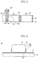
- FIG. 3 is a sectional view showing removal of the molten material.
- a blade 100 having a width of x1 is moved in a direction toward the viewer (or away from the viewer) along the through hole 54 to remove the molten material 20A.
- a dicing trace is formed on the side surface upper portion 16A with the blade 100, the side surface upper portion 16A thereby being caused to have a surface roughness Rz of 1.0 ⁇ m or less.
- the molten material 20A is not entirely removed, the molten material 20 is left on side surface lower portions.
- the adhesive 14 is Ag paste having electrical conductivity.
- the adhesive 14 may be formed of a material in liquid or film form.
- the adhesive is cured.
- This process step is referred to as an adhesive curing step.
- the adhesive 14 is cured by heating or UV application. Wire bonding is performed as desired on electrode pads 18 after the adhesive curing step.
- Figure 5 shows photographs for comparison between the surface roughness Rz of the device side surface after laser dicing and the surface roughness Rz after blade dicing.
- Laser dicing photographs A to D show side surface conditions and surface roughnesses when laser dicing was performed by using four oscillators differing in oscillation frequency.
- the surface roughness Rz of the device side surface as a result of laser dicing is 4 to 12 ⁇ m.
- the surface roughness Rz of the device side surface when blade dicing was performed was 1 ⁇ m or less. Accordingly, the surface roughness Rz of the side surface upper portion 16A formed by blade dicing is 1 ⁇ m or less, while the surface roughness Rz of the side surface lower portion 16B formed by laser dicing is 4.0 ⁇ m or more.
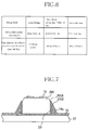
- Figure 6 is a table showing, with respect to dicing methods, the surface roughness Rz of the device side surface and the time taken for the adhesive to climb up to the device upper surface.
- the surface roughness Rz of the device side surface is high and the time taken for the adhesive to climb up to the device upper surface is short.
- the surface roughness Rz of the device side surface is low and the time taken for the adhesive to climb up to the device upper surface is long.
- the surface roughness Rz of the device side surface upper portion 16A is 1.0 ⁇ m or less. Therefore, even if the standby time period from the completion of the die bonding step to the adhesive curing step is increased, it is possible to prevent the adhesive 14 from reaching the device upper surface by climbing up on the device side surface. Setting a long standby time period enables adoption of batch processing with higher production efficiency.
- the surface roughness Rz of the side surface upper portion 16A is reduced, it is possible to prevent the adhesive 14 from reaching the device upper surface even if the amount of the adhesive 14 varies largely. Climbing up of the adhesive 14 can thus be presented by the side surface upper portion 16A.
- a wider choice of adhesives can therefore be provided.
- a highly functional heat-conductive adhesive an adhesive capable of improving the joining strength, an adhesive having high wettability or an adhesive of a low viscosity can be used.
- the wafer is first fully cut by laser dicing capable of high-speed dicing and the part of the molten material 20A is thereafter removed with the blade 100. Dicing can thereby by completed in a short time in comparison with full cutting of the wafer with a blade, thus enabling improving the productivity.
- the mode in which only the molten material on the side surface upper portion is removed is adopted for the purpose of achieving a processing speed higher than that in the case of removing the entire molten material and for the purpose of reducing the amount of wear of the blade and the frequency of blade replacement operation.
- the necessary dicing street width is ordinarily 50 to 100 ⁇ m.
- the blade width xl can be within the range from 10 to 20 ⁇ m and the number of devices to be taken can therefore be increased by reducing the width of the dicing street.
- the surface roughnesses Rz of the side surface upper portion 16A and the side surface lower portion 16B are not limited to the above-mentioned values. Climbing up of the adhesive 14 can be prevented as long as the surface roughness of the side surface upper portion 16A is set lower than the surface roughness of the side surface lower portion 16B by using the semiconductor device manufacturing method according to Embodiment 1 of the present invention.
- the device according to Embodiment 1 of the present invention can adopt various materials which are not limited to GaAs.
- the device may be formed of a ceramic. While the molten material 20 is removed with the blade 100, wet etching or dry etching may be performed to remove the molten material 20. While the molten material on the side surface upper portion of the device is removed in the removal step, the molten material on the entire side surface may be removed. Any adhesive may suffice if it is capable of bonding the mount substrate and the device to each other. The adhesive is not limited to electrically conductive materials. These modifications can also be applied to Embodiment 2 described below.
- FIG. 7 is a sectional view of a semiconductor device according to Embodiment 2 of the present invention.
- a lower surface of a device 200 is fixed to a mount substrate 12 with the adhesive 14.
- a side surface upper portion 200A of the device 200 is a slanting surface.
- a dicing trace with a surface roughness Rz of 1.0 ⁇ m or less is formed on a side surface upper portion 200A.
- a molten material 20 is formed on a side surface lower portion 200B as a result of melting of GaAs caused by laser dicing.
- the molten material 20 is a dicing trace formed by laser dicing.
- the side surface lower portion 200B is therefore a rough surface having a surface roughness Rz of 4.0 ⁇ m or more.
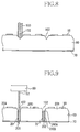
- FIG. 8 is a sectional view of the wafer, showing forming of grooves in the wafer.
- Grooves 102 are formed in a wafer 60 with the blade 100. Grooves 102 are formed along dicing streets.
- Figure 9 is a sectional view of the wafer, showing a state of laser dicing.
- Laser dicing is performed on the portions in which the grooves 102 are formed, as seen in plan, with portions of the grooves 102 left. Through holes 201 and 202 are formed thereby.
- the wafer is thereby separated into individual devices 200, 204, and 206. This process step is referred to as a laser dicing step.
- the molten material 20 is formed on the side surface lower portions 200B by laser dicing.
- This process step is a die bonding step. Subsequently, after a lapse of a standby time period, the process advances to an adhesive curing step. In the adhesive curing step, the adhesive 14 is cured by heating or UV application. Subsequently, a wire bonding step is performed as desired.
- the side surface upper portions 200A with a low surface roughness are formed by forming the grooves 102 with the blade 100. Subsequently, individual devices are separated by laser dicing, with the side surface upper portions 200A left thereon. Thus, the surface roughness of the side surface upper portions 200A can be reduced and climbing up of the adhesive can therefore be prevented.
- the grooves 102 may be formed by etching instead of being formed with the blade 100. Description of symbols
- 10 semiconductor device, 12 mount substrate, 14 adhesive, 14a a part of the adhesive, 16 device, 16A side surface upper portion, 16B side surface lower portion, 18 electrode pads, 20,20A molten material, 50 laser device, 52 laser light, 54,56 through hole, 60 wafer, 70 dicing tape, 100 blade, 102 grooves, 200 device, 200A side surface upper portion, 200B side surface lower portion, 201,202 through holes
Landscapes
- Dicing (AREA)
- Physics & Mathematics (AREA)
- Electromagnetism (AREA)
- Optics & Photonics (AREA)
- Laser Beam Processing (AREA)
- Die Bonding (AREA)
Abstract
Description
- The present invention relates to a semiconductor device having a diced device fixed on a mount substrate with an adhesive and a method of manufacturing the semiconductor device.
- An operation to cut a wafer or the like along longitudinal and lateral directions to separate the wafer into individual devices (chips) is called dicing. There are chiefly three methods of dicing. The first of them is a blade dicing method in which an extremely thin circular blade called a diamond blade is rotated at a high speed to cut a wafer.
- The second is a scribe breaking in which a wafer is scribed with an edge of a diamond and mechanical stress is thereafter produced in the wafer to cut the wafer. The third is a laser dicing method in which a wafer is cut by using laser light. By laser dicing, laser energy is concentrated to sublimate, melt or ionize a portion of a wafer material, thereby separating the wafer into individual devices.
-
Patent Literature 1 discloses a dicing technique using a combination of laser dicing and blade dicing. In this technique, a laser beam is applied along a dicing street on a wafer to form a worked groove, and the wafer is cut along the worked groove by using a blade. - Patent Literature 1: Japanese Patent Laid-Open No.
2012-4478 - Laser dicing is of a high throughput and high yield in comparison with blade dicing and scribe breaking. Further, laser dicing is capable of reducing the cut width (dicing street width) and, therefore, capable of increasing the number of devices taken.
- However, when a wafer or the like is diced by laser dicing, molten material is formed on side surfaces of the device. There is a problem that when die bonding is performed by bringing a device lower surface into contact with an adhesive, the adhesive climbs up along the molten material on the device side surfaces to reach a device upper surface. Electrode pads on the device upper surface are thereby contaminated, thereby reducing the strength of joining between the electrode pads and wires. In a case where an electrically conductive adhesive is used, there is a problem that an electrical short occurs due to the adhesive having climbed up onto the device upper surface.
- In the technique disclosed in
Patent Literature 1, almost the entire wafer is cut by blade dicing and there is, therefore, a problem that the blade moving speed cannot be increased and the productivity cannot be improved. - The present invention has been achieved to solve the above-described problems, and an object of the present invention is to provide a semiconductor device capable of preventing climbing up of an adhesive while improving the productivity and a method of manufacturing the semiconductor device.
- According to the present invention, there is provided a semiconductor device including a mount substrate, an adhesive applied to the mount substrate, and a device having its lower surface bonded to the mount substrate with the adhesive, wherein the surface roughness of a side surface upper portion of the device is lower than that of a side surface lower portion of the device.
- According to the present invention, there is also provided a semiconductor device manufacturing method including a laser dicing step of separating a wafer into individual devices by forming through holes in the wafer by laser dicing, a removal step of removing, with a blade or by etching, a molten material formed on side surfaces of the device in the laser dicing step, a die bonding step of bonding a mount substrate and a lower surface of the device to each other with an adhesive after the removal step, and an adhesive curing step of curing the adhesive.
- According to the present invention, a semiconductor device capable of preventing climbing up of an adhesive while improving the productivity can be provided.
-
-
Figure 1 is a sectional view of a semiconductor device according toEmbodiment 1 of the present invention. -
Figure 2 is a sectional view of a wafer showing a state of laser dicing. -
Figure 3 is a sectional view showing removal of the molten material. -
Figure 4 is sectional view showing the die bonding step. -
Figure 5 shows photographs for comparison between the surface roughness Rz of the device side surface after laser dicing and the surface roughness Rz after blade dicing. -
Figure 6 is table showing, with respect to dicing methods, the surface roughness Rz of the device side surface and the time taken for the adhesive to climb up to the device upper surface. -
Figure 7 is a sectional view of a semiconductor device according to Embodiment 2 of the present invention. -
Figure 8 is a sectional view of the wafer, showing forming of grooves in the wafer. -
Figure 9 is a sectional view of the wafer, showing a state of laser dicing. - A semiconductor device and a semiconductor device manufacturing method according to an embodiment of the present invention will be described with reference to the drawings. Components identical or corresponding to each other are indicated by the same reference characters and repeated description for them is omitted in some cases.
-
Figure 1 is a sectional view of a semiconductor device according toEmbodiment 1 of the present invention. Asemiconductor device 10 has amount substrate 12. Anadhesive 14 is applied to themount substrate 12. Themount substrate 12 and a lower surface of adevice 16 are bonded to each other with theadhesive 14. Thedevice 16 is formed, for example, of a compound semiconductor such as GaAs. An upper surface of thedevice 16 is an active region on whichelectrode pads 18 are formed. - A dicing trace with a surface roughness Rz of 1.0 µm or less is formed on a side surface
upper portion 16A of thedevice 16. Amolten material 20 is formed on a side surfacelower portion 16B of thedevice 16 as a result of melting of GaAs caused by laser dicing. Themolten material 20 is a dicing trace formed by laser dicing. Themolten material 20 is porous and has minute cracks. Accordingly, the side surfacelower portion 16B of thedevice 16 is a rough surface having a surface roughness Rz of 4.0 µm or more. - A
part 14a of the adhesive 14 climbs up on the side surfacelower portion 16B high in surface roughness Rz. Thepart 14a of theadhesive 14, however, does not reach the side surfaceupper portion 16A low in surface roughness Rz. - A method of manufacturing the
semiconductor device 10 will be described. Laser dicing is first performed on a wafer.Figure 2 is a sectional view of a wafer showing a state of laser dicing. Awafer 60 is diced withlaser light 52 emitted after being amplified in alaser device 50. Throughholes wafer 60, thereby separating intoindividual devices dicing tape 70 to a lower surface of thewafer 60. - A
molten material 20A produced at the time of laser dicing is formed on side surfaces of each device. The sum of the width of the throughhole 54 and the widths of themolten material 20A on opposite sides of the throughhole 54 is x1. The value xl is, for example, in the range from 10 to 20 µm. - Subsequently, the
molten material 20A formed on the side surfaces of the devices in the laser dicing step is removed with a blade. This process step is referred to as removal step.Figure 3 is a sectional view showing removal of the molten material. Ablade 100 having a width of x1 is moved in a direction toward the viewer (or away from the viewer) along the throughhole 54 to remove themolten material 20A. A dicing trace is formed on the side surfaceupper portion 16A with theblade 100, the side surfaceupper portion 16A thereby being caused to have a surface roughness Rz of 1.0 µm or less. In this step, themolten material 20A is not entirely removed, themolten material 20 is left on side surface lower portions. - After the removal step, the mount substrate and the lower surface of the device are bonded to each other with the adhesive. This process step is referred to as a die bonding step.
Figure 4 is a sectional view showing the die bonding step. The adhesive 14 is Ag paste having electrical conductivity. For example, the adhesive 14 may be formed of a material in liquid or film form. - After a lapse of a certain "standby time period" from the completion of the die bonding step, the adhesive is cured. This process step is referred to as an adhesive curing step. In the adhesive curing step, the adhesive 14 is cured by heating or UV application. Wire bonding is performed as desired on
electrode pads 18 after the adhesive curing step. -
Figure 5 shows photographs for comparison between the surface roughness Rz of the device side surface after laser dicing and the surface roughness Rz after blade dicing. Laser dicing photographs A to D show side surface conditions and surface roughnesses when laser dicing was performed by using four oscillators differing in oscillation frequency. The surface roughness Rz of the device side surface as a result of laser dicing is 4 to 12 µm. - The surface roughness Rz of the device side surface when blade dicing was performed was 1 µm or less. Accordingly, the surface roughness Rz of the side surface
upper portion 16A formed by blade dicing is 1 µm or less, while the surface roughness Rz of the side surfacelower portion 16B formed by laser dicing is 4.0 µm or more. -
Figure 6 is a table showing, with respect to dicing methods, the surface roughness Rz of the device side surface and the time taken for the adhesive to climb up to the device upper surface. In the case of laser dicing, the surface roughness Rz of the device side surface is high and the time taken for the adhesive to climb up to the device upper surface is short. On the other hand, in the case of blade dicing or scribe breaking, the surface roughness Rz of the device side surface is low and the time taken for the adhesive to climb up to the device upper surface is long. - In the
semiconductor device 10 according toEmbodiment 1 of the present invention, the surface roughness Rz of the device side surfaceupper portion 16A is 1.0 µm or less. Therefore, even if the standby time period from the completion of the die bonding step to the adhesive curing step is increased, it is possible to prevent the adhesive 14 from reaching the device upper surface by climbing up on the device side surface. Setting a long standby time period enables adoption of batch processing with higher production efficiency. - Since the surface roughness Rz of the side surface
upper portion 16A is reduced, it is possible to prevent the adhesive 14 from reaching the device upper surface even if the amount of the adhesive 14 varies largely. Climbing up of the adhesive 14 can thus be presented by the side surfaceupper portion 16A. A wider choice of adhesives can therefore be provided. For example, a highly functional heat-conductive adhesive, an adhesive capable of improving the joining strength, an adhesive having high wettability or an adhesive of a low viscosity can be used. - When an operation to fully cut the wafer by blade dicing is performed, the blade moving speed cannot be increased and the productivity cannot be improved. In the semiconductor device manufacturing method according to
Embodiment 1 of the present invention, however, the wafer is first fully cut by laser dicing capable of high-speed dicing and the part of themolten material 20A is thereafter removed with theblade 100. Dicing can thereby by completed in a short time in comparison with full cutting of the wafer with a blade, thus enabling improving the productivity. The mode in which only the molten material on the side surface upper portion is removed is adopted for the purpose of achieving a processing speed higher than that in the case of removing the entire molten material and for the purpose of reducing the amount of wear of the blade and the frequency of blade replacement operation. - In blade dicing methods, the necessary dicing street width is ordinarily 50 to 100 µm. In laser dicing according to the present invention, however, the blade width xl can be within the range from 10 to 20 µm and the number of devices to be taken can therefore be increased by reducing the width of the dicing street.
- The surface roughnesses Rz of the side surface
upper portion 16A and the side surfacelower portion 16B are not limited to the above-mentioned values. Climbing up of the adhesive 14 can be prevented as long as the surface roughness of the side surfaceupper portion 16A is set lower than the surface roughness of the side surfacelower portion 16B by using the semiconductor device manufacturing method according toEmbodiment 1 of the present invention. - The device according to
Embodiment 1 of the present invention can adopt various materials which are not limited to GaAs. For example, the device may be formed of a ceramic. While themolten material 20 is removed with theblade 100, wet etching or dry etching may be performed to remove themolten material 20. While the molten material on the side surface upper portion of the device is removed in the removal step, the molten material on the entire side surface may be removed. Any adhesive may suffice if it is capable of bonding the mount substrate and the device to each other. The adhesive is not limited to electrically conductive materials. These modifications can also be applied to Embodiment 2 described below. - A semiconductor device and a semiconductor device manufacturing method according to Embodiment 2 have a number of commonalities with
Embodiment 1, and will therefore be described mainly with respect to points of difference fromEmbodiment 1.Figure 7 is a sectional view of a semiconductor device according to Embodiment 2 of the present invention. In this semiconductor device, a lower surface of adevice 200 is fixed to amount substrate 12 with the adhesive 14. - A side surface
upper portion 200A of thedevice 200 is a slanting surface. A dicing trace with a surface roughness Rz of 1.0 µm or less is formed on a side surfaceupper portion 200A. Amolten material 20 is formed on a side surfacelower portion 200B as a result of melting of GaAs caused by laser dicing. Themolten material 20 is a dicing trace formed by laser dicing. The side surfacelower portion 200B is therefore a rough surface having a surface roughness Rz of 4.0 µm or more. - A semiconductor device manufacturing method according to Embodiment 2 of the present invention will be described. Grooves are first formed in a wafer.
Figure 8 is a sectional view of the wafer, showing forming of grooves in the wafer.Grooves 102 are formed in awafer 60 with theblade 100.Grooves 102 are formed along dicing streets. - Subsequently, laser dicing is performed.
Figure 9 is a sectional view of the wafer, showing a state of laser dicing. Laser dicing is performed on the portions in which thegrooves 102 are formed, as seen in plan, with portions of thegrooves 102 left. Throughholes individual devices molten material 20 is formed on the side surfacelower portions 200B by laser dicing. - Subsequently, the
mount substrate 12 and a lower surface of thedevice 200 are bonded to each other with the adhesive 14. This process step is a die bonding step. Subsequently, after a lapse of a standby time period, the process advances to an adhesive curing step. In the adhesive curing step, the adhesive 14 is cured by heating or UV application. Subsequently, a wire bonding step is performed as desired. - In the semiconductor device according to Embodiment 2 of the present invention, the side surface
upper portions 200A with a low surface roughness are formed by forming thegrooves 102 with theblade 100. Subsequently, individual devices are separated by laser dicing, with the side surfaceupper portions 200A left thereon. Thus, the surface roughness of the side surfaceupper portions 200A can be reduced and climbing up of the adhesive can therefore be prevented. Thegrooves 102 may be formed by etching instead of being formed with theblade 100. Description of symbols - 10 semiconductor device, 12 mount substrate, 14 adhesive, 14a a part of the adhesive, 16 device, 16A side surface upper portion, 16B side surface lower portion, 18 electrode pads, 20,20A molten material, 50 laser device, 52 laser light, 54,56 through hole, 60 wafer, 70 dicing tape, 100 blade, 102 grooves, 200 device, 200A side surface upper portion, 200B side surface lower portion, 201,202 through holes
Claims (5)
- A semiconductor device comprising:a mount substrate;an adhesive applied to the mount substrate; anda device having its lower surface bonded to the mount substrate with the adhesive,wherein the surface roughness of a side surface upper portion of the device is lower than that of a side surface lower portion of the device.
- The semiconductor device according to Claim 1, wherein a dicing trace with a surface roughness Rz of 1.0 µm or less is formed on a side surface upper portion of the device, and
a dicing trace with a surface roughness Rz of 4.0 µm or more is formed on a side surface lower portion of the device. - A semiconductor device manufacturing method comprising:a laser dicing step of separating a wafer into individual devices by forming through holes in the wafer by laser dicing;a removal step of removing, with a blade or by etching, a molten material formed on side surfaces of the device in the laser dicing step;a die bonding step of bonding a mount substrate and a lower surface of the device to each other with an adhesive after the removal step; andan adhesive curing step of curing the adhesive.
- The semiconductor device manufacturing method according to Claim 3, wherein in the removal step, only the molten material formed on the side surface upper portions of the device is removed.
- A semiconductor device manufacturing method comprising:a step of forming grooves in a wafer with blade or by etching;a laser dicing step of forming through holes by performing laser dicing on the portions in which the grooves are formed, as seen in plan, with portions of the grooves left, the wafer being separated into individual devices;a die bonding step of bonding a mount substrate and a lower surface of the device to each other with an adhesive; andan adhesive curing step of curing the adhesive.
Applications Claiming Priority (2)
| Application Number | Priority Date | Filing Date | Title |
|---|---|---|---|
| JP2013082088 | 2013-04-10 | ||
| PCT/JP2013/077979 WO2014167745A1 (en) | 2013-04-10 | 2013-10-15 | Semiconductor device and semiconductor device manufacturing method |
Publications (3)
| Publication Number | Publication Date |
|---|---|
| EP2985785A1 true EP2985785A1 (en) | 2016-02-17 |
| EP2985785A4 EP2985785A4 (en) | 2017-01-11 |
| EP2985785B1 EP2985785B1 (en) | 2023-12-20 |
Family
ID=51689169
Family Applications (1)
| Application Number | Title | Priority Date | Filing Date |
|---|---|---|---|
| EP13881860.4A Active EP2985785B1 (en) | 2013-04-10 | 2013-10-15 | Method of manufacturing a semiconductor device with prevention of adhesive climbing up and corresponding semiconductor device |
Country Status (7)
| Country | Link |
|---|---|
| US (1) | US11233029B2 (en) |
| EP (1) | EP2985785B1 (en) |
| JP (1) | JP6304243B2 (en) |
| KR (2) | KR101823851B1 (en) |
| CN (1) | CN105103278B (en) |
| TW (1) | TWI511239B (en) |
| WO (1) | WO2014167745A1 (en) |
Families Citing this family (11)
| Publication number | Priority date | Publication date | Assignee | Title |
|---|---|---|---|---|
| KR102506441B1 (en) | 2017-12-04 | 2023-03-06 | 삼성전자주식회사 | Fabrication method of semiconductor light emitting array and semiconductor light emitting array |
| CN109683218B (en) | 2018-01-25 | 2022-02-15 | 苏州旭创科技有限公司 | Optical element, optical module, and method for manufacturing the same |
| JP7047922B2 (en) * | 2018-09-04 | 2022-04-05 | 株式会社村田製作所 | Manufacturing method of MEMS device and MEMS device |
| DE102019124181B4 (en) * | 2018-09-28 | 2023-06-15 | Taiwan Semiconductor Manufacturing Co., Ltd. | Singulation method for stacked semiconductor components and stacked semiconductor device |
| US11081392B2 (en) * | 2018-09-28 | 2021-08-03 | Taiwan Semiconductor Manufacturing Co., Ltd. | Dicing method for stacked semiconductor devices |
| CN114178710B (en) * | 2020-08-24 | 2024-11-26 | 奥特斯(中国)有限公司 | Component carrier and method for manufacturing the same |
| JP7549214B2 (en) * | 2020-10-30 | 2024-09-11 | 日亜化学工業株式会社 | Light emitting device and method for manufacturing the same |
| US12100697B2 (en) * | 2021-02-25 | 2024-09-24 | Advanced Semiconductor Engineering, Inc. | Semiconductor package structure |
| JPWO2023139902A1 (en) * | 2022-01-21 | 2023-07-27 | ||
| WO2023176370A1 (en) * | 2022-03-17 | 2023-09-21 | ローム株式会社 | Semiconductor element and semiconductor device |
| FR3155443A1 (en) * | 2023-11-20 | 2025-05-23 | Commissariat à l'Energie Atomique et aux Energies Alternatives | Process for manufacturing elementary cells to be characterized |
Family Cites Families (33)
| Publication number | Priority date | Publication date | Assignee | Title |
|---|---|---|---|---|
| JPH09172029A (en) * | 1995-12-19 | 1997-06-30 | Hitachi Ltd | Semiconductor chip, manufacturing method thereof, and semiconductor device |
| TW502408B (en) * | 2001-03-09 | 2002-09-11 | Advanced Semiconductor Eng | Chip with chamfer |
| US6888259B2 (en) | 2001-06-07 | 2005-05-03 | Denso Corporation | Potted hybrid integrated circuit |
| JP2003243797A (en) | 2002-02-19 | 2003-08-29 | Matsushita Electric Ind Co Ltd | Module parts |
| WO2003090258A2 (en) | 2002-04-19 | 2003-10-30 | Xsil Technology Limited | Laser machining |
| WO2005096399A1 (en) | 2004-03-31 | 2005-10-13 | Nichia Corporation | Nitride semiconductor light emitting element |
| JP4683989B2 (en) | 2004-04-20 | 2011-05-18 | 昭和電工株式会社 | Compound semiconductor light emitting device wafer manufacturing method |
| EP1738419B1 (en) | 2004-04-20 | 2012-07-11 | Showa Denko K.K. | Production method of compound semiconductor light-emitting device wafer |
| JP4476087B2 (en) | 2004-09-27 | 2010-06-09 | シャープ株式会社 | Method for manufacturing light-emitting diode element |
| TWI269392B (en) | 2005-03-03 | 2006-12-21 | Advanced Semiconductor Eng | Die structure of package and method of manufacturing the same |
| JP2006253298A (en) | 2005-03-09 | 2006-09-21 | Toshiba Corp | Semiconductor light emitting device and semiconductor light emitting device |
| JP4992220B2 (en) * | 2005-10-12 | 2012-08-08 | 日亜化学工業株式会社 | Manufacturing method of semiconductor device |
| JP2008166445A (en) * | 2006-12-27 | 2008-07-17 | Enzan Seisakusho Co Ltd | Semiconductor substrate cutting method |
| JP2009004625A (en) | 2007-06-22 | 2009-01-08 | Sanken Electric Co Ltd | Semiconductor light emitting device |
| US7786600B2 (en) * | 2008-06-30 | 2010-08-31 | Hynix Semiconductor Inc. | Circuit substrate having circuit wire formed of conductive polarization particles, method of manufacturing the circuit substrate and semiconductor package having the circuit wire |
| JP5193809B2 (en) * | 2008-11-05 | 2013-05-08 | 新光電気工業株式会社 | Wiring board and manufacturing method thereof |
| WO2010073583A1 (en) * | 2008-12-24 | 2010-07-01 | 住友ベークライト株式会社 | Adhesive film, multilayer circuit substrate, component for semiconductor, and semiconductor device |
| JP2010186916A (en) * | 2009-02-13 | 2010-08-26 | Renesas Electronics Corp | Method of manufacturing semiconductor device |
| US9048404B2 (en) * | 2009-07-06 | 2015-06-02 | Zhuo Sun | Thin flat solid state light source module |
| JP5368957B2 (en) * | 2009-12-04 | 2013-12-18 | シャープ株式会社 | Manufacturing method of semiconductor laser chip |
| JP2011129612A (en) * | 2009-12-16 | 2011-06-30 | Renesas Electronics Corp | Method for manufacturing semiconductor device and semiconductor device |
| WO2011112707A2 (en) * | 2010-03-10 | 2011-09-15 | University Of Maine System Board Of Trustees | Attachment of a device to a substrate for operation under variable conditions |
| WO2011113480A1 (en) * | 2010-03-16 | 2011-09-22 | Arena Distribution S.A. | Swim cap, particularly for users having long hair |
| JP5474630B2 (en) * | 2010-03-30 | 2014-04-16 | トッパン・フォームズ株式会社 | Electronic component and manufacturing method thereof, component mounting board |
| JP5604186B2 (en) | 2010-06-21 | 2014-10-08 | 株式会社ディスコ | Processing equipment |
| DE102010032755B4 (en) * | 2010-07-29 | 2019-05-23 | Siemens Healthcare Gmbh | Method of visualizing an atrium of the heart of a patient |
| JP5770446B2 (en) | 2010-09-30 | 2015-08-26 | 株式会社ディスコ | Split method |
| JP5251991B2 (en) * | 2011-01-14 | 2013-07-31 | トヨタ自動車株式会社 | Semiconductor module |
| TW201242122A (en) * | 2011-04-15 | 2012-10-16 | Chi Mei Lighting Tech Corp | Light-emitting diode device |
| US20120306031A1 (en) * | 2011-05-31 | 2012-12-06 | Freescale Semiconductor, Inc. | Semiconductor sensor device and method of packaging same |
| JP2013004528A (en) | 2011-06-10 | 2013-01-07 | Panasonic Corp | Semiconductor device and manufacturing method of the same |
| US8906782B2 (en) * | 2011-11-07 | 2014-12-09 | Infineon Technologies Ag | Method of separating semiconductor die using material modification |
| JP5050127B1 (en) * | 2011-12-13 | 2012-10-17 | 株式会社タカハシ抜型製作所 | Welding method for punched blade joints |
-
2013
- 2013-10-15 EP EP13881860.4A patent/EP2985785B1/en active Active
- 2013-10-15 CN CN201380075504.3A patent/CN105103278B/en not_active Expired - Fee Related
- 2013-10-15 JP JP2015511072A patent/JP6304243B2/en not_active Expired - Fee Related
- 2013-10-15 KR KR1020177032180A patent/KR101823851B1/en not_active Expired - Fee Related
- 2013-10-15 WO PCT/JP2013/077979 patent/WO2014167745A1/en not_active Ceased
- 2013-10-15 KR KR1020157025408A patent/KR20150119350A/en not_active Ceased
- 2013-10-15 US US14/766,414 patent/US11233029B2/en not_active Expired - Fee Related
- 2013-11-22 TW TW102142594A patent/TWI511239B/en not_active IP Right Cessation
Also Published As
| Publication number | Publication date |
|---|---|
| JP6304243B2 (en) | 2018-04-04 |
| WO2014167745A1 (en) | 2014-10-16 |
| KR101823851B1 (en) | 2018-01-30 |
| EP2985785A4 (en) | 2017-01-11 |
| US20150371966A1 (en) | 2015-12-24 |
| EP2985785B1 (en) | 2023-12-20 |
| CN105103278A (en) | 2015-11-25 |
| US11233029B2 (en) | 2022-01-25 |
| TW201440179A (en) | 2014-10-16 |
| TWI511239B (en) | 2015-12-01 |
| KR20150119350A (en) | 2015-10-23 |
| JPWO2014167745A1 (en) | 2017-02-16 |
| CN105103278B (en) | 2018-11-27 |
| KR20170127041A (en) | 2017-11-20 |
Similar Documents
| Publication | Publication Date | Title |
|---|---|---|
| US11233029B2 (en) | Semiconductor device having a device fixed on a substrate with an adhesive | |
| US11145548B2 (en) | Manufacturing process of element chip using laser grooving and plasma-etching | |
| CN100466184C (en) | wafer processing method | |
| CN105340065B (en) | Semiconductive pieces manufacture method, the circuit board containing semiconductive pieces and electronic equipment, method for dividing substrate | |
| JP2004031526A (en) | Manufacturing method of group iii nitride compound semiconductor element | |
| JP6100396B2 (en) | Semiconductor device manufacturing method and semiconductor device | |
| CN104690429A (en) | Processing method for optical device wafer | |
| TWI603391B (en) | Laser cutting method for semiconductor wafer | |
| US20220238343A1 (en) | Singulation of silicon carbide semiconductor wafers | |
| CN107210334B (en) | Method for producing a plurality of semiconductor chips and semiconductor chip | |
| JP2002319554A (en) | Method and device for dividing wafer | |
| JP2013161944A (en) | Dicing method | |
| US12476170B2 (en) | High voltage flip-chip on lead (FOL) package | |
| JP6591240B2 (en) | Device manufacturing method | |
| JP2014090117A (en) | Semiconductor device, semiconductor device mounting structure and semiconductor device manufacturing method | |
| US20150364374A1 (en) | Semiconductor Device Die Singulation by Discontinuous Laser Scribe and Break | |
| KR19990075107A (en) | Structure of cutting blade for semiconductor wafer and cutting method using the same | |
| HK40057577A (en) | Semiconductor chip manufacturing device and method for manufacturing semiconductor chip |
Legal Events
| Date | Code | Title | Description |
|---|---|---|---|
| PUAI | Public reference made under article 153(3) epc to a published international application that has entered the european phase |
Free format text: ORIGINAL CODE: 0009012 |
|
| 17P | Request for examination filed |
Effective date: 20150812 |
|
| AK | Designated contracting states |
Kind code of ref document: A1 Designated state(s): AL AT BE BG CH CY CZ DE DK EE ES FI FR GB GR HR HU IE IS IT LI LT LU LV MC MK MT NL NO PL PT RO RS SE SI SK SM TR |
|
| AX | Request for extension of the european patent |
Extension state: BA ME |
|
| DAX | Request for extension of the european patent (deleted) | ||
| RIC1 | Information provided on ipc code assigned before grant |
Ipc: H01L 21/60 20060101ALI20160905BHEP Ipc: H01L 23/485 20060101ALI20160905BHEP Ipc: H01L 21/78 20060101AFI20160905BHEP |
|
| A4 | Supplementary search report drawn up and despatched |
Effective date: 20161212 |
|
| RIC1 | Information provided on ipc code assigned before grant |
Ipc: H01L 21/60 20060101ALI20161206BHEP Ipc: H01L 21/78 20060101AFI20161206BHEP Ipc: H01L 23/485 20060101ALI20161206BHEP |
|
| STAA | Information on the status of an ep patent application or granted ep patent |
Free format text: STATUS: EXAMINATION IS IN PROGRESS |
|
| 17Q | First examination report despatched |
Effective date: 20190514 |
|
| REG | Reference to a national code |
Ref country code: DE Ref legal event code: R079 Free format text: PREVIOUS MAIN CLASS: H01L0021520000 Ipc: H01L0021600000 Ref country code: DE Ref legal event code: R079 Ref document number: 602013085088 Country of ref document: DE Free format text: PREVIOUS MAIN CLASS: H01L0021520000 Ipc: H01L0021600000 |
|
| GRAP | Despatch of communication of intention to grant a patent |
Free format text: ORIGINAL CODE: EPIDOSNIGR1 |
|
| STAA | Information on the status of an ep patent application or granted ep patent |
Free format text: STATUS: GRANT OF PATENT IS INTENDED |
|
| RIC1 | Information provided on ipc code assigned before grant |
Ipc: H01L 23/488 20060101ALI20230925BHEP Ipc: H01L 21/78 20060101ALI20230925BHEP Ipc: H01L 21/60 20060101AFI20230925BHEP |
|
| GRAS | Grant fee paid |
Free format text: ORIGINAL CODE: EPIDOSNIGR3 |
|
| INTG | Intention to grant announced |
Effective date: 20231016 |
|
| GRAA | (expected) grant |
Free format text: ORIGINAL CODE: 0009210 |
|
| STAA | Information on the status of an ep patent application or granted ep patent |
Free format text: STATUS: THE PATENT HAS BEEN GRANTED |
|
| P01 | Opt-out of the competence of the unified patent court (upc) registered |
Effective date: 20231027 |
|
| AK | Designated contracting states |
Kind code of ref document: B1 Designated state(s): AL AT BE BG CH CY CZ DE DK EE ES FI FR GB GR HR HU IE IS IT LI LT LU LV MC MK MT NL NO PL PT RO RS SE SI SK SM TR |
|
| REG | Reference to a national code |
Ref country code: GB Ref legal event code: FG4D |
|
| REG | Reference to a national code |
Ref country code: CH Ref legal event code: EP |
|
| REG | Reference to a national code |
Ref country code: DE Ref legal event code: R096 Ref document number: 602013085088 Country of ref document: DE |
|
| REG | Reference to a national code |
Ref country code: IE Ref legal event code: FG4D |
|
| REG | Reference to a national code |
Ref country code: NL Ref legal event code: FP |
|
| PG25 | Lapsed in a contracting state [announced via postgrant information from national office to epo] |
Ref country code: GR Free format text: LAPSE BECAUSE OF FAILURE TO SUBMIT A TRANSLATION OF THE DESCRIPTION OR TO PAY THE FEE WITHIN THE PRESCRIBED TIME-LIMIT Effective date: 20240321 |
|
| REG | Reference to a national code |
Ref country code: LT Ref legal event code: MG9D |
|
| PG25 | Lapsed in a contracting state [announced via postgrant information from national office to epo] |
Ref country code: LT Free format text: LAPSE BECAUSE OF FAILURE TO SUBMIT A TRANSLATION OF THE DESCRIPTION OR TO PAY THE FEE WITHIN THE PRESCRIBED TIME-LIMIT Effective date: 20231220 |
|
| PG25 | Lapsed in a contracting state [announced via postgrant information from national office to epo] |
Ref country code: ES Free format text: LAPSE BECAUSE OF FAILURE TO SUBMIT A TRANSLATION OF THE DESCRIPTION OR TO PAY THE FEE WITHIN THE PRESCRIBED TIME-LIMIT Effective date: 20231220 |
|
| PG25 | Lapsed in a contracting state [announced via postgrant information from national office to epo] |
Ref country code: LT Free format text: LAPSE BECAUSE OF FAILURE TO SUBMIT A TRANSLATION OF THE DESCRIPTION OR TO PAY THE FEE WITHIN THE PRESCRIBED TIME-LIMIT Effective date: 20231220 Ref country code: GR Free format text: LAPSE BECAUSE OF FAILURE TO SUBMIT A TRANSLATION OF THE DESCRIPTION OR TO PAY THE FEE WITHIN THE PRESCRIBED TIME-LIMIT Effective date: 20240321 Ref country code: FI Free format text: LAPSE BECAUSE OF FAILURE TO SUBMIT A TRANSLATION OF THE DESCRIPTION OR TO PAY THE FEE WITHIN THE PRESCRIBED TIME-LIMIT Effective date: 20231220 Ref country code: ES Free format text: LAPSE BECAUSE OF FAILURE TO SUBMIT A TRANSLATION OF THE DESCRIPTION OR TO PAY THE FEE WITHIN THE PRESCRIBED TIME-LIMIT Effective date: 20231220 Ref country code: BG Free format text: LAPSE BECAUSE OF FAILURE TO SUBMIT A TRANSLATION OF THE DESCRIPTION OR TO PAY THE FEE WITHIN THE PRESCRIBED TIME-LIMIT Effective date: 20240320 |
|
| REG | Reference to a national code |
Ref country code: AT Ref legal event code: MK05 Ref document number: 1643194 Country of ref document: AT Kind code of ref document: T Effective date: 20231220 |
|
| PG25 | Lapsed in a contracting state [announced via postgrant information from national office to epo] |
Ref country code: SE Free format text: LAPSE BECAUSE OF FAILURE TO SUBMIT A TRANSLATION OF THE DESCRIPTION OR TO PAY THE FEE WITHIN THE PRESCRIBED TIME-LIMIT Effective date: 20231220 Ref country code: RS Free format text: LAPSE BECAUSE OF FAILURE TO SUBMIT A TRANSLATION OF THE DESCRIPTION OR TO PAY THE FEE WITHIN THE PRESCRIBED TIME-LIMIT Effective date: 20231220 Ref country code: NO Free format text: LAPSE BECAUSE OF FAILURE TO SUBMIT A TRANSLATION OF THE DESCRIPTION OR TO PAY THE FEE WITHIN THE PRESCRIBED TIME-LIMIT Effective date: 20240320 Ref country code: LV Free format text: LAPSE BECAUSE OF FAILURE TO SUBMIT A TRANSLATION OF THE DESCRIPTION OR TO PAY THE FEE WITHIN THE PRESCRIBED TIME-LIMIT Effective date: 20231220 Ref country code: HR Free format text: LAPSE BECAUSE OF FAILURE TO SUBMIT A TRANSLATION OF THE DESCRIPTION OR TO PAY THE FEE WITHIN THE PRESCRIBED TIME-LIMIT Effective date: 20231220 |
|
| PG25 | Lapsed in a contracting state [announced via postgrant information from national office to epo] |
Ref country code: IS Free format text: LAPSE BECAUSE OF FAILURE TO SUBMIT A TRANSLATION OF THE DESCRIPTION OR TO PAY THE FEE WITHIN THE PRESCRIBED TIME-LIMIT Effective date: 20240420 |
|
| PG25 | Lapsed in a contracting state [announced via postgrant information from national office to epo] |
Ref country code: CZ Free format text: LAPSE BECAUSE OF FAILURE TO SUBMIT A TRANSLATION OF THE DESCRIPTION OR TO PAY THE FEE WITHIN THE PRESCRIBED TIME-LIMIT Effective date: 20231220 Ref country code: AT Free format text: LAPSE BECAUSE OF FAILURE TO SUBMIT A TRANSLATION OF THE DESCRIPTION OR TO PAY THE FEE WITHIN THE PRESCRIBED TIME-LIMIT Effective date: 20231220 |
|
| PG25 | Lapsed in a contracting state [announced via postgrant information from national office to epo] |
Ref country code: SK Free format text: LAPSE BECAUSE OF FAILURE TO SUBMIT A TRANSLATION OF THE DESCRIPTION OR TO PAY THE FEE WITHIN THE PRESCRIBED TIME-LIMIT Effective date: 20231220 |
|
| PG25 | Lapsed in a contracting state [announced via postgrant information from national office to epo] |
Ref country code: SM Free format text: LAPSE BECAUSE OF FAILURE TO SUBMIT A TRANSLATION OF THE DESCRIPTION OR TO PAY THE FEE WITHIN THE PRESCRIBED TIME-LIMIT Effective date: 20231220 Ref country code: SK Free format text: LAPSE BECAUSE OF FAILURE TO SUBMIT A TRANSLATION OF THE DESCRIPTION OR TO PAY THE FEE WITHIN THE PRESCRIBED TIME-LIMIT Effective date: 20231220 Ref country code: RO Free format text: LAPSE BECAUSE OF FAILURE TO SUBMIT A TRANSLATION OF THE DESCRIPTION OR TO PAY THE FEE WITHIN THE PRESCRIBED TIME-LIMIT Effective date: 20231220 Ref country code: IT Free format text: LAPSE BECAUSE OF FAILURE TO SUBMIT A TRANSLATION OF THE DESCRIPTION OR TO PAY THE FEE WITHIN THE PRESCRIBED TIME-LIMIT Effective date: 20231220 Ref country code: IS Free format text: LAPSE BECAUSE OF FAILURE TO SUBMIT A TRANSLATION OF THE DESCRIPTION OR TO PAY THE FEE WITHIN THE PRESCRIBED TIME-LIMIT Effective date: 20240420 Ref country code: EE Free format text: LAPSE BECAUSE OF FAILURE TO SUBMIT A TRANSLATION OF THE DESCRIPTION OR TO PAY THE FEE WITHIN THE PRESCRIBED TIME-LIMIT Effective date: 20231220 Ref country code: CZ Free format text: LAPSE BECAUSE OF FAILURE TO SUBMIT A TRANSLATION OF THE DESCRIPTION OR TO PAY THE FEE WITHIN THE PRESCRIBED TIME-LIMIT Effective date: 20231220 Ref country code: AT Free format text: LAPSE BECAUSE OF FAILURE TO SUBMIT A TRANSLATION OF THE DESCRIPTION OR TO PAY THE FEE WITHIN THE PRESCRIBED TIME-LIMIT Effective date: 20231220 |
|
| PG25 | Lapsed in a contracting state [announced via postgrant information from national office to epo] |
Ref country code: PT Free format text: LAPSE BECAUSE OF FAILURE TO SUBMIT A TRANSLATION OF THE DESCRIPTION OR TO PAY THE FEE WITHIN THE PRESCRIBED TIME-LIMIT Effective date: 20240422 Ref country code: PL Free format text: LAPSE BECAUSE OF FAILURE TO SUBMIT A TRANSLATION OF THE DESCRIPTION OR TO PAY THE FEE WITHIN THE PRESCRIBED TIME-LIMIT Effective date: 20231220 |
|
| PG25 | Lapsed in a contracting state [announced via postgrant information from national office to epo] |
Ref country code: PT Free format text: LAPSE BECAUSE OF FAILURE TO SUBMIT A TRANSLATION OF THE DESCRIPTION OR TO PAY THE FEE WITHIN THE PRESCRIBED TIME-LIMIT Effective date: 20240422 Ref country code: PL Free format text: LAPSE BECAUSE OF FAILURE TO SUBMIT A TRANSLATION OF THE DESCRIPTION OR TO PAY THE FEE WITHIN THE PRESCRIBED TIME-LIMIT Effective date: 20231220 |
|
| REG | Reference to a national code |
Ref country code: DE Ref legal event code: R097 Ref document number: 602013085088 Country of ref document: DE |
|
| PG25 | Lapsed in a contracting state [announced via postgrant information from national office to epo] |
Ref country code: DK Free format text: LAPSE BECAUSE OF FAILURE TO SUBMIT A TRANSLATION OF THE DESCRIPTION OR TO PAY THE FEE WITHIN THE PRESCRIBED TIME-LIMIT Effective date: 20231220 |
|
| PLBE | No opposition filed within time limit |
Free format text: ORIGINAL CODE: 0009261 |
|
| STAA | Information on the status of an ep patent application or granted ep patent |
Free format text: STATUS: NO OPPOSITION FILED WITHIN TIME LIMIT |
|
| PG25 | Lapsed in a contracting state [announced via postgrant information from national office to epo] |
Ref country code: SI Free format text: LAPSE BECAUSE OF FAILURE TO SUBMIT A TRANSLATION OF THE DESCRIPTION OR TO PAY THE FEE WITHIN THE PRESCRIBED TIME-LIMIT Effective date: 20231220 |
|
| PG25 | Lapsed in a contracting state [announced via postgrant information from national office to epo] |
Ref country code: SI Free format text: LAPSE BECAUSE OF FAILURE TO SUBMIT A TRANSLATION OF THE DESCRIPTION OR TO PAY THE FEE WITHIN THE PRESCRIBED TIME-LIMIT Effective date: 20231220 Ref country code: DK Free format text: LAPSE BECAUSE OF FAILURE TO SUBMIT A TRANSLATION OF THE DESCRIPTION OR TO PAY THE FEE WITHIN THE PRESCRIBED TIME-LIMIT Effective date: 20231220 |
|
| 26N | No opposition filed |
Effective date: 20240923 |
|
| REG | Reference to a national code |
Ref country code: DE Ref legal event code: R119 Ref document number: 602013085088 Country of ref document: DE |
|
| REG | Reference to a national code |
Ref country code: CH Ref legal event code: PL |
|
| REG | Reference to a national code |
Ref country code: NL Ref legal event code: MM Effective date: 20241101 |
|
| GBPC | Gb: european patent ceased through non-payment of renewal fee |
Effective date: 20241015 |
|
| PG25 | Lapsed in a contracting state [announced via postgrant information from national office to epo] |
Ref country code: MC Free format text: LAPSE BECAUSE OF FAILURE TO SUBMIT A TRANSLATION OF THE DESCRIPTION OR TO PAY THE FEE WITHIN THE PRESCRIBED TIME-LIMIT Effective date: 20231220 |
|
| PG25 | Lapsed in a contracting state [announced via postgrant information from national office to epo] |
Ref country code: DE Free format text: LAPSE BECAUSE OF NON-PAYMENT OF DUE FEES Effective date: 20250501 |
|
| PG25 | Lapsed in a contracting state [announced via postgrant information from national office to epo] |
Ref country code: GB Free format text: LAPSE BECAUSE OF NON-PAYMENT OF DUE FEES Effective date: 20241015 |
|
| PG25 | Lapsed in a contracting state [announced via postgrant information from national office to epo] |
Ref country code: BE Free format text: LAPSE BECAUSE OF NON-PAYMENT OF DUE FEES Effective date: 20241031 Ref country code: NL Free format text: LAPSE BECAUSE OF NON-PAYMENT OF DUE FEES Effective date: 20241101 Ref country code: LU Free format text: LAPSE BECAUSE OF NON-PAYMENT OF DUE FEES Effective date: 20241015 |
|
| PG25 | Lapsed in a contracting state [announced via postgrant information from national office to epo] |
Ref country code: FR Free format text: LAPSE BECAUSE OF NON-PAYMENT OF DUE FEES Effective date: 20241031 |
|
| PG25 | Lapsed in a contracting state [announced via postgrant information from national office to epo] |
Ref country code: CH Free format text: LAPSE BECAUSE OF NON-PAYMENT OF DUE FEES Effective date: 20241031 |
|
| REG | Reference to a national code |
Ref country code: BE Ref legal event code: MM Effective date: 20241031 |
|
| PG25 | Lapsed in a contracting state [announced via postgrant information from national office to epo] |
Ref country code: IE Free format text: LAPSE BECAUSE OF NON-PAYMENT OF DUE FEES Effective date: 20241015 |
|
| PG25 | Lapsed in a contracting state [announced via postgrant information from national office to epo] |
Ref country code: CY Free format text: LAPSE BECAUSE OF FAILURE TO SUBMIT A TRANSLATION OF THE DESCRIPTION OR TO PAY THE FEE WITHIN THE PRESCRIBED TIME-LIMIT; INVALID AB INITIO Effective date: 20131015 |
|
| PG25 | Lapsed in a contracting state [announced via postgrant information from national office to epo] |
Ref country code: HU Free format text: LAPSE BECAUSE OF FAILURE TO SUBMIT A TRANSLATION OF THE DESCRIPTION OR TO PAY THE FEE WITHIN THE PRESCRIBED TIME-LIMIT; INVALID AB INITIO Effective date: 20131015 |