EP2985644B1 - Procédé de fabrication d'un guide optique - Google Patents
Procédé de fabrication d'un guide optique Download PDFInfo
- Publication number
- EP2985644B1 EP2985644B1 EP15180212.1A EP15180212A EP2985644B1 EP 2985644 B1 EP2985644 B1 EP 2985644B1 EP 15180212 A EP15180212 A EP 15180212A EP 2985644 B1 EP2985644 B1 EP 2985644B1
- Authority
- EP
- European Patent Office
- Prior art keywords
- layer
- semiconductor
- dielectric layer
- thickness
- substrate
- Prior art date
- Legal status (The legal status is an assumption and is not a legal conclusion. Google has not performed a legal analysis and makes no representation as to the accuracy of the status listed.)
- Not-in-force
Links
Images

Classifications
-
- G—PHYSICS
- G02—OPTICS
- G02B—OPTICAL ELEMENTS, SYSTEMS OR APPARATUS
- G02B6/00—Light guides; Structural details of arrangements comprising light guides and other optical elements, e.g. couplings
- G02B6/10—Light guides; Structural details of arrangements comprising light guides and other optical elements, e.g. couplings of the optical waveguide type
- G02B6/12—Light guides; Structural details of arrangements comprising light guides and other optical elements, e.g. couplings of the optical waveguide type of the integrated circuit kind
- G02B6/13—Integrated optical circuits characterised by the manufacturing method
- G02B6/131—Integrated optical circuits characterised by the manufacturing method by using epitaxial growth
-
- G—PHYSICS
- G02—OPTICS
- G02B—OPTICAL ELEMENTS, SYSTEMS OR APPARATUS
- G02B6/00—Light guides; Structural details of arrangements comprising light guides and other optical elements, e.g. couplings
- G02B6/10—Light guides; Structural details of arrangements comprising light guides and other optical elements, e.g. couplings of the optical waveguide type
- G02B6/107—Subwavelength-diameter waveguides, e.g. nanowires
-
- G—PHYSICS
- G02—OPTICS
- G02B—OPTICAL ELEMENTS, SYSTEMS OR APPARATUS
- G02B6/00—Light guides; Structural details of arrangements comprising light guides and other optical elements, e.g. couplings
- G02B6/10—Light guides; Structural details of arrangements comprising light guides and other optical elements, e.g. couplings of the optical waveguide type
- G02B6/12—Light guides; Structural details of arrangements comprising light guides and other optical elements, e.g. couplings of the optical waveguide type of the integrated circuit kind
- G02B6/13—Integrated optical circuits characterised by the manufacturing method
- G02B6/136—Integrated optical circuits characterised by the manufacturing method by etching
-
- G—PHYSICS
- G02—OPTICS
- G02F—OPTICAL DEVICES OR ARRANGEMENTS FOR THE CONTROL OF LIGHT BY MODIFICATION OF THE OPTICAL PROPERTIES OF THE MEDIA OF THE ELEMENTS INVOLVED THEREIN; NON-LINEAR OPTICS; FREQUENCY-CHANGING OF LIGHT; OPTICAL LOGIC ELEMENTS; OPTICAL ANALOGUE/DIGITAL CONVERTERS
- G02F1/00—Devices or arrangements for the control of the intensity, colour, phase, polarisation or direction of light arriving from an independent light source, e.g. switching, gating or modulating; Non-linear optics
- G02F1/01—Devices or arrangements for the control of the intensity, colour, phase, polarisation or direction of light arriving from an independent light source, e.g. switching, gating or modulating; Non-linear optics for the control of the intensity, phase, polarisation or colour
- G02F1/015—Devices or arrangements for the control of the intensity, colour, phase, polarisation or direction of light arriving from an independent light source, e.g. switching, gating or modulating; Non-linear optics for the control of the intensity, phase, polarisation or colour based on semiconductor elements having potential barriers, e.g. having a PN or PIN junction
- G02F1/025—Devices or arrangements for the control of the intensity, colour, phase, polarisation or direction of light arriving from an independent light source, e.g. switching, gating or modulating; Non-linear optics for the control of the intensity, phase, polarisation or colour based on semiconductor elements having potential barriers, e.g. having a PN or PIN junction in an optical waveguide structure
-
- B—PERFORMING OPERATIONS; TRANSPORTING
- B82—NANOTECHNOLOGY
- B82Y—SPECIFIC USES OR APPLICATIONS OF NANOSTRUCTURES; MEASUREMENT OR ANALYSIS OF NANOSTRUCTURES; MANUFACTURE OR TREATMENT OF NANOSTRUCTURES
- B82Y20/00—Nanooptics, e.g. quantum optics or photonic crystals
-
- G—PHYSICS
- G02—OPTICS
- G02B—OPTICAL ELEMENTS, SYSTEMS OR APPARATUS
- G02B6/00—Light guides; Structural details of arrangements comprising light guides and other optical elements, e.g. couplings
- G02B6/10—Light guides; Structural details of arrangements comprising light guides and other optical elements, e.g. couplings of the optical waveguide type
- G02B6/12—Light guides; Structural details of arrangements comprising light guides and other optical elements, e.g. couplings of the optical waveguide type of the integrated circuit kind
- G02B2006/12035—Materials
- G02B2006/12061—Silicon
-
- G—PHYSICS
- G02—OPTICS
- G02B—OPTICAL ELEMENTS, SYSTEMS OR APPARATUS
- G02B6/00—Light guides; Structural details of arrangements comprising light guides and other optical elements, e.g. couplings
- G02B6/10—Light guides; Structural details of arrangements comprising light guides and other optical elements, e.g. couplings of the optical waveguide type
- G02B6/12—Light guides; Structural details of arrangements comprising light guides and other optical elements, e.g. couplings of the optical waveguide type of the integrated circuit kind
- G02B2006/12133—Functions
- G02B2006/12142—Modulator
Definitions
- the present invention relates to a method of manufacturing an optical guide.
- the invention relates to the field of optical guides with vertical slit used in particular for electro-optical modulators of the capacitive type.
- These optical guides can also be used in particular as optical switches, light sources or optical sensors.
- the optical guide comprises two crystalline semiconductor regions separated by a dielectric layer, the dielectric layer having a predetermined width and a predetermined thickness strictly greater than said width.
- the dielectric layer forms the vertical slit.
- the two crystalline semiconductor regions can be electrically doped and form a capacitance with the dielectric layer.
- the charge carriers accumulate at the interfaces between the dielectric layer and the semiconductor regions.
- This variation in the concentration of charge carriers can lead to the phenomenon of electro-refraction, that is to say that the refractive index of the semiconductor regions varies locally according to the potential difference of the electric field applied.
- the optical field is essentially confined in the dielectric layer, which makes it possible to reduce optical losses.
- This variation in the refractive index of the semiconductor regions makes it possible to introduce a phase shift for an electromagnetic wave propagating through the semiconductor regions.
- an interferometric structure is associated with the optical guide to obtain an intensity modulation from the phase shift introduced.
- the interferometric structure can be a Mach-Zehnder, Fabry-Pérot or ring type interferometer.
- a first method of manufacturing an optical guide known from the state of the art, in particular from the document FR 2 907 916 is a method of manufacturing an optical guide comprising two crystalline semiconductor regions separated by a dielectric layer, the dielectric layer having a predetermined width and a predetermined thickness strictly greater than said width, the method comprising the steps: a) providing a substrate successively comprising an electrical insulating layer and a crystalline semiconductor layer, the substrate having a flat surface, b) forming a trench in the semiconducting layer so as to expose the electric insulating layer and delimit first and second semiconductor zones on either side of the exposed electrically insulating layer, step b) being carried out so that the first semiconductor zone has a lateral edge extending over the entire the thickness of the semiconductor layer and along an axis perpendicular to the flat surface of the substrate, the first semiconductor zone being intended to form the first semiconductor region of the optical guide, c) forming the dielectric layer of the predetermined width over the entire thickness of the side edge.
- width is meant a dimension along an axis parallel to the plane defined by the flat surface of the substrate.
- thickness is meant a dimension along an axis perpendicular to the flat surface of the substrate.
- crystalline is meant an area or a region in which the atoms or molecules are arranged regularly in a characteristic pattern, which therefore excludes the amorphous areas or regions.
- perpendicular is meant that the angle formed between the side edge and the flat surface of the substrate is between 85 ° and 95 °.
- the trench formed during step b) is configured to have a constant width equal to the predetermined width of the layer dielectric.
- the exposed electrically insulating layer thus has a width equal to the predetermined width of the dielectric layer.
- Step c) is carried out by plasma-assisted chemical vapor deposition.
- the dielectric layer formed during step c) may include a bubble when the ratio between the thickness and the width of the dielectric layer is greater than 1.5 , as specified on page 3, lines 22 to 28.
- This bubble is highly detrimental in terms of performance of the optical guide, as specified on page 3, lines 29 to 31.
- step b) of forming the trench must be perfectly mastered because it determines the width of the dielectric layer.
- a second method of manufacturing an optical guide known from the state of the art, in particular from the document EP 2,463,695 is a method of manufacturing an optical guide comprising two crystalline semiconductor regions separated by a dielectric layer, the dielectric layer having a predetermined width and a predetermined thickness strictly greater than said width, the method comprising the steps: a) providing a substrate successively comprising a layer of electrical insulation and a crystalline semiconductor layer, the substrate having a flat surface, b) forming a trench in the semiconductor layer so as to expose the layer of electrical insulation and delimit first and second semiconductor zones on either side of the exposed electrically insulating layer.
- Step b) is followed by a step of depositing a dielectric material on the exposed electrically insulating layer, the deposited dielectric material having a thickness equal to the predetermined thickness of the dielectric layer.
- the deposited dielectric material is then etched so as to keep only one slit of the predetermined width, the slit forming the dielectric layer of the optical guide.
- This second process is not entirely satisfactory insofar as obtaining a fine slit (30 to 50 nm) requires several etchings of the dielectric material, as specified in ⁇ 0027, which makes the second process complex to implement. with an extension of the operating time. Furthermore, the cleaning steps after said etchings lead to imperfect control of the uniformity of the thickness of the slit, the second process not thus being perfectly reproducible.
- Alexander Spott et al "Photolithographic fabrication of slot waveguides", ADVANCED FABRICATION TECHNOLOGIES FOR MICRO / NANO OPTICS AND PHOTONICS IV, vol. 7927, no. 1 , describes a method of manufacturing an optical guide comprising two crystalline semiconductor regions, the dielectric layer having a predetermined width and a predetermined thickness greater than said width, the method comprising the steps: a) providing a substrate successively comprising a layer of electrical insulator and a crystalline semiconductor layer, the substrate having a planar surface, b) forming a trench in the semiconductor layer so as to expose the layer of electrical insulator and delimit first and second semi-areas -conductors on either side of the exposed electrical insulating layer, c) forming the dielectric layer in the trench.
- the present invention aims to remedy all or part of the aforementioned drawbacks, and for this purpose relates to a method of manufacturing an optical guide comprising two crystalline semiconductor regions separated by a dielectric layer, the dielectric layer having a predetermined width and a predetermined thickness strictly greater than said width, the method comprising the steps: a) providing a substrate successively comprising an electrical insulating layer and a crystalline semiconductor layer, the substrate having a flat surface, b) forming a trench in the layer semiconductor so as to expose the electric insulating layer and delimit first and second semiconductor zones on either side of the exposed electrically insulating layer, step b) being performed from so that the first semiconductor zone has a lateral edge extending over the entire thickness of the semiconductor layer and along an axis perp endicular to the flat surface of the substrate, the first semiconductor zone being intended to form the first semiconductor region of the optical guide, c) forming the dielectric layer of the predetermined width over the entire thickness of the lateral edge, the method being remarkable in that the trench formed during step
- width is meant a dimension along an axis parallel to the plane defined by the flat surface of the substrate.
- thickness is meant a dimension along an axis perpendicular to the flat surface of the substrate.
- crystalline is meant an area or a region in which the atoms or molecules are arranged regularly in a characteristic pattern, which therefore excludes the amorphous areas or regions.
- perpendicular is meant that the angle formed between the side edge and the flat surface of the substrate is between 85 ° and 95 °.
- seed layer is meant a thin layer forming an epitaxial growth support of a crystalline material.
- Such a method according to the invention makes it possible to avoid the formation of a bubble inside the dielectric layer by a width of the exposed electrical insulating layer sufficiently large relative to the thickness of the layer. germ.
- the width of the dielectric layer is entirely determined during step c) in the absence of geometric constraint due to a sufficiently low thickness of the seed layer.
- the width of the dielectric layer is therefore not determined by the width of the layer of electrical insulation exposed during step b).
- the width of the exposed electrically insulating layer thus constitutes an adjustment variable relative to the desired thickness of the seed layer in order to avoid the formation of a bubble inside the dielectric layer. It is then possible to envisage the formation of a dielectric layer having a ratio between the thickness and the width much greater than 1.5, for example between 17 and 50, preferably between 20 and 50, still preferably between between 20 and 30.
- Step d) must be performed after step c) in order to avoid the formation of a bubble inside the dielectric layer, due to geometric constraints appearing with the thickness of the epitaxial layer.
- such a method according to the invention makes it possible to obtain good uniformity of the thickness and of the width of the dielectric layer, and this with a limited duration of operation.
- the present invention also relates to a method of manufacturing an optical guide comprising two crystalline semiconductor regions separated by a dielectric layer, the dielectric layer having a predetermined width and a predetermined thickness strictly greater than said width, the method comprising the steps: a) providing a substrate successively comprising an electrical insulating layer and a crystalline semiconductor layer, the substrate having a flat surface, the substrate being based on a crystalline semiconductor material, b) removing part of the layer semiconductor so as to expose the electrically insulating layer and delimit a single semiconductor area on one side of the exposed electrically insulating layer, step b) being performed so that the area semiconductor has a side edge extending over the entire thickness of the semiconductor layer and along an axis perpendicular to the flat surface of the su bstrat, the semiconductor zone being intended to form the first semiconductor region of the optical guide, c) forming the dielectric layer of the predetermined width over the entire thickness of the lateral edge, c1) forming at least one trench in the layer of electrical insulator exposed so
- width is meant a dimension along an axis parallel to the plane defined by the flat surface of the substrate.
- thickness is meant a dimension along an axis perpendicular to the flat surface of the substrate.
- crystalline is meant an area or a region in which the atoms or molecules are arranged regularly in a characteristic pattern, which therefore excludes the amorphous areas or regions.
- perpendicular is meant that the angle formed between the side edge and the flat surface of the substrate is between 85 ° and 95 °.
- such a method according to the invention makes it possible to avoid the formation of a bubble inside the dielectric layer because the dielectric layer is formed during step c) in the absence of a semi-conductive zone in sight of the single semiconductor zone delimited during step b). More precisely, there is no semiconductor zone facing the single semiconductor zone along the width of the optical guide.
- the width of the dielectric layer is entirely determined during step c) in the absence of geometric constraint due to the absence of a semiconductor zone facing the single semiconductor zone delimited during l 'step b). It is then possible to envisage the formation of a dielectric layer having a ratio between the thickness and the width much greater than 1.5, for example between 17 and 50, preferably between 20 and 50, still preferably between between 20 and 30.
- such a method according to the invention makes it possible to obtain uniformity of the thickness and of the width of the dielectric layer, and this with a limited operating time.
- steps c) and c1) can be inverted indifferently.
- step d) must be carried out after step c) in order to avoid the formation of a bubble inside the dielectric layer, and this because of geometric constraints appearing with the thickness of the epitaxial layer.
- the inventive concept common to the two methods according to the invention is the formation of the dielectric layer during step c) in the absence of geometric constraints, or by a thickness of the seed layer sufficiently low, or by the absence of a semi-conductor zone facing each other along the width of the optical guide.
- Such a concept makes it possible to envisage a ratio between the thickness and the width of the dielectric layer much greater than 1.5.
- such a concept makes it possible to obtain uniformity of the thickness and of the width of the dielectric layer, and this with a duration of dielectric layer. restricted operation.
- step b) is performed by an etching of the semiconductor layer suitable for forming the seed layer and part of the lateral edge of the first semiconductor zone, said etching comprising an overetching of the semiconductor layer suitable for exposing the electric insulating layer and delimiting the seed layer of the first semiconductor zone, the overetching completing the formation of the lateral edge of the first semiconductor zone.
- the etching of the semiconductor layer is a reactive ionic etching adapted to favor anisotropic etching, the overetching of the semiconductor layer being obtained by an oblique incidence of an ionic flux.
- privileged is meant that the parameters of reactive ionic etching such as pressure, power, temperature and bias voltage are chosen so as to favor anisotropic plasma etching over dry etching. isotropic chemical. For example, a low bias voltage, high pressure and temperature make it possible to favor dry chemical etching. On the other hand, a high polarization voltage, a low pressure make it possible to favor a plasma etching by promoting the mechanical ion bombardment.
- high and “low” will be appreciated by those skilled in the art in particular as a function of the material to be etched and of the reactive gases chosen for the plasma.
- the choice of reactive ionic etching makes it possible to perform step b) within a single frame.
- the overetching obtained makes a trench, and is known under the name of "trenching" in English, described for example in the book entitled “Plasma Etching in Microelectronics”, N. Layadi et al., 2001 .
- the topography of the engraved object leads to an oblique incidence of an ionic flux on a zone of the lateral edge of the first semiconductor zone and / or on a zone of the flank of the engraving mask.
- the zone of the lateral edge of the first semiconductor zone and / or the zone of the flank of the etching mask deflects the incident ionic flux. This results in a concentration of the ionic flux appearing at the foot of the lateral edge of the first semiconductor zone.
- step b) is performed by an anisotropic etching, such as reactive ionic etching, adapted to form the side edge of the semiconductor zone.
- step c) is carried out by thermal oxidation of the side edge.
- thermal oxidation allows control of the width of the dielectric layer formed on the thickness of the side edge. Further, thermal oxidation consumes the crystalline material extending from the side edge. As a result, thermal oxidation does not require any particular constraint on the width of the layer of electrical insulation exposed during step b). Thus, the width of the layer of electrical insulation exposed during step c) may be less than the predetermined width of the dielectric layer. In contrast, thermal oxidation also consumes the crystalline material of the seed layer. It is therefore necessary to provide during step b) a sufficient thickness for the seed layer so that the thickness of the seed layer after step c) is sufficient for a resumption of epitaxy.
- step c) is performed by a conformal deposition of the dielectric layer on the side edge, preferably by atomic layer deposition or by plasma-assisted chemical vapor deposition.
- the thickness of the seed layer is strictly less than 1.5 times the width of the exposed electrical insulation layer.
- Formal is meant that the dielectric layer formed retains the topography of the surface on which said dielectric layer has been deposited.
- the crystalline material extending from the side edge is not consumed.
- the width of the layer of electrical insulation exposed during step c) must be greater than the predetermined width of the dielectric layer.
- the additional geometric condition on the thickness of the seed layer makes it possible to avoid the formation of a bubble inside the dielectric layer for certain types of conformal deposition.
- step d) comprises a mechanical-chemical polishing step adapted to make the second semiconductor region coplanar with the dielectric layer and with the first semiconductor region.
- the semiconductor layer is monocrystalline, preferably based on monocrystalline silicon.
- the monocrystalline structure of the semiconductor layer makes it possible to reduce the optical losses relative to a polycrystalline structure for example.
- the semiconductor layer has a thickness equal to the predetermined thickness of the dielectric layer.
- a step of etching the dielectric layer is avoided after the formation of the dielectric layer on the side edge during step c). Further, a step of epitaxy of the first semiconductor region is also avoided.
- the method comprises a step of electrically doping the first and second semiconductor regions so that the optical guide forms a capacitor.
- Such a manufactured optical guide is very particularly suitable for an electro-optical modulator of the capacitive type.
- the ratio between the thickness and the width of the dielectric layer formed during step c) is greater than 1.5.
- the present invention also relates to an optical guide capable of being obtained by a method in accordance with the invention when the ratio between the thickness and the width of the dielectric layer formed during step c) is greater than 1.5.
- Such an optical guide differs from the state of the art by a width of the dielectric layer that is uniform and can be controlled, with a view to production on an industrial scale.
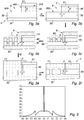
- the first process illustrated in figures 1a to 1g is a method of manufacturing an optical guide 1 comprising two semiconductor regions 10, 11 crystallines separated by a dielectric layer 2, as shown figure 1g .
- the dielectric layer 2 has a predetermined width l and a predetermined thickness e strictly greater than said width l; e> l.
- the first method comprises a step a) providing a substrate 3 successively comprising a support substrate 32, an electrical insulating layer 30 and a crystalline semiconductor layer 31.
- the substrate 3 has a flat surface 310.
- the flat surface 310 of the substrate 3 corresponds to the free surface of the semiconductor layer 31.
- the semiconductor layer 31 advantageously has a thickness E equal to the predetermined thickness e of the layer. dielectric 2.
- width is meant a dimension along an axis X'-X parallel to the plane defined by the flat surface 310 of the substrate 3.
- thickness is understood to mean a dimension along a Z'-Z axis perpendicular to the flat surface 310 of the substrate 3.
- the semiconductor layer 31 is advantageously monocrystalline, preferably based on monocrystalline silicon.
- the first method comprises a step b) forming a trench 4 in the semiconductor layer 31 so as to expose the electrically insulating layer 30 and delimit first and second semiconductor zones 40, 41 on both sides. other of the exposed electrically insulating layer 300.
- Step b) comprises a preliminary step illustrated in figure 1b consisting in arranging an etching mask 5 on the semiconductor layer 31 to protect the first semiconductor zone 40.
- the etching mask 5 preferably comprises a hard mask layer 51 arranged on the semiconductor layer 31 and a layer 50 based on photosensitive resin on top of the hard mask layer 51.
- the etching mask 5 can be formed from a single layer 50 based on photosensitive resin or from a single layer 51 of hard mask.
- Step b) is carried out so that the first semiconductor zone 40 has a lateral edge 400 extending over the entire thickness E of the semiconductor layer 31 and along a Z'-Z axis perpendicular to the flat surface 310 of the substrate 3.
- perpendicular is meant that the angle formed between the side edge 400 and the flat surface 310 of the substrate 3 is between 85 ° and 95 °.
- the first semiconductor zone 40 is intended to form the first semiconductor region 10 of the optical guide 1.
- the trench formed during step b) is configured so that the second semiconductor zone 41 forms a seed layer s 'extending over a thickness e 0 strictly less than the thickness E of the semiconductor layer 31.
- Step b) is performed by an etching of the semiconductor layer 31 adapted to form the seed layer and part of the side edge 400 of the first conductive zone 40.
- the etching comprises an overetching of the semiconductor layer 31 adapted. to expose the electrically insulating layer 30 and delimit the seed layer of the first semiconductor zone 40.
- the overetching completes the formation of the lateral edge 400 of the first semiconductor zone 40.
- the width 10 of the exposed electrical insulating layer 300 obtained after step b) is preferably between 10 nm and 50 nm.
- the thickness e 0 of the seed layer obtained after step b) is preferably between 10 nm and 70 nm.
- Step b) is advantageously carried out by reactive ionic etching of the semiconductor layer 31 adapted to favor anisotropic etching.
- the overetching of the semiconductor layer 31 is obtained by an oblique incidence of an ionic flux.
- oblique is meant a direction which is not parallel to the Z'-Z axis. More precisely, the topography of the engraved object leads to an oblique incidence of an ionic flux on a zone of the lateral edge 400 of the first semiconductor zone 40 and / or on a zone of the flank of the etching mask 5.
- the zone of the lateral edge 400 of the first semiconductor zone and / or the zone of the flank of the etching mask 5 deviates the incident ionic flux. This results in a concentration of ionic flux appearing at the foot of the lateral edge 400 of the first semiconductor zone 40.
- the anisotropy of the etching is favored for example by the choice of the respective power of the upper generator and the lower generator, denoted Psup and Pinf.
- the upper generator has a high power relative to the power of the lower generator, preferably Psup> 3 Pinf.
- Psup 3 Pinf.
- the pressure inside the chamber can be less than 6.7 Pa (50 mTorr), from preferably less than 1.3 Pa (10 mTorr).
- the reactive gases introduced into the chamber are advantageously chosen from the group comprising Cl 2 , HBr, O 2 He and CF 4 .
- the trench produced by the overetching can be obtained by a high Cl 2 / HBr ratio and a low pressure inside the chamber.
- the Cl 2 / HBr ratio is advantageously of the order of 3: 1, and the pressure inside the chamber is of the order of 0.5 Pa (4 mTorr).
- the reactive gas flows (in sccm) for Cl 2 , HBr, O 2 He and CF 4 are respectively of the order of 150, 50, 5 and 10.
- the trench produced by the overetching then presents a depth of the order of 40 nm, which corresponds to the thickness e 0 of the seed layer obtained after step b).
- the ratio between the thickness e 0 of the seed layer obtained after step b) and the width l 0 of the exposed electrical insulating layer 300 obtained after step b) is of the order of 1.
- the thickness of the hard mask layer 51 to be etched is predetermined in particular as a function of the thickness E of the semiconductor layer 31 and of the etching speed differential between the layer 51 and the semiconductor layer 31.
- a dielectric layer 2 based on SiO 2 This results in the formation of a dielectric layer 2 based on SiO 2 .
- a layer of SiO 2 is formed around the seed layer 41, as visible at figure 1d .
- the SiO 2 layer formed around the seed layer 41 is removed before step d) described below, preferably by anisotropic etching.
- step c) determines the duration of execution of step c) according to the desired width l of the dielectric layer 2.
- the thermal oxidation also consuming the crystalline material of the seed layer, the trench formed during step b) is previously configured so that the thickness of the seed layer after step c) is sufficient for a resumption of epitaxy.
- step c) is performed by a conformal deposition of the dielectric layer 2 on the lateral edge 400.
- the conformal deposition is preferably an atomic layer deposition -ALD- or an assisted chemical vapor deposition. by plasma -PECVD-.
- step c) is advantageously carried out by a deposition PECVD of SiO 2 at a temperature between 350 ° C and 400 ° C with a source of tetraethyl orthosilicate -TEOS.
- the trench formed during step b) is then configured beforehand so that the second semiconductor zone 41 forms a seed layer extending over a thickness e 0 strictly less than 1.5 times the width l 0 of the layer electrical insulation stripped 300; e 0 ⁇ 1.5 l 0 .
- the first method comprises a step d) forming by epitaxy the second semiconductor region 11 of the optical guide 1 from the seed layer 41.
- the epitaxy of step d) is selective so as to avoid growth at from the exposed electrically insulating layer 300.
- Step d) is performed after step c).
- step d) advantageously comprises a mechanical-chemical polishing step adapted to make the second semiconductor region 11 coplanar with the dielectric layer 2 and with the first semiconductor region 10.
- the hard mask layer 51 makes it possible to protect the first semiconductor zone 40 of the chemical mechanical polishing.
- the first method advantageously comprises a step (not illustrated) of electrically doping the first and second semiconductor regions 10, 11 so that the optical guide 1 forms a capacitor.
- the ratio between the thickness e and the width l of the dielectric layer 2 of the optical guide 1 obtained is advantageously greater than 1.5.
- the width l of the dielectric layer 2 is less than or equal to 50 nm and greater than or equal to 5 nm.
- the width l of the dielectric layer 2 is between 10 nm and 20 nm.
- the ratio between the thickness e and the width l of the dielectric layer 2 is between 17 and 50, preferably between 20 and 50, even more preferably between 20 and 30.
- the second process illustrated in figures 2a to 2e is a method of manufacturing an optical guide 1 comprising two crystalline semiconductor regions 10, 11 separated by a dielectric layer 2, as shown figure 2f .
- the dielectric layer 2 has a predetermined width l and a predetermined thickness e strictly greater than said width l; e> l.
- the second method comprises a step a) providing a substrate 3 successively comprising a support substrate 32, an electrical insulating layer 30 and a crystalline semiconductor layer.
- the substrate 3 has a flat surface 310.
- the support substrate 32 is based on a crystalline semiconductor material.
- the support substrate 32 is advantageously monocrystalline, preferably based on monocrystalline silicon.
- the semiconductor layer advantageously has a thickness E equal to the predetermined thickness e of the dielectric layer 2.
- width is meant a dimension along an axis X'-X parallel to the plane defined by the flat surface 310 of the substrate 3.
- thickness is understood to mean a dimension along a Z'-Z axis perpendicular to the flat surface 310 of the substrate 3.
- the semiconductor layer is advantageously monocrystalline, preferably based on monocrystalline silicon.
- the second method comprises a step b) removing a part 4 of the semiconductor layer so as to expose the electric insulating layer 30 and delimiting a single semiconductor zone 40 on one side of the layer of exposed electrical insulator 300.
- Step b) comprises a preliminary step (not illustrated) consisting in arranging an etching mask on the semiconductor layer to protect the semiconductor zone 40.
- the etching mask preferably comprises a layer 51 of a hard mask arranged on the semiconductor layer and a photosensitive resin-based layer surmounting the hard mask layer 51.
- step b) is performed so that the semiconductor zone 40 has a lateral edge 400 extending over the entire thickness E of the semiconductor layer and along an axis perpendicular to the flat surface 310 of the substrate 3 .
- perpendicular is meant that the angle formed between the side edge 400 and the flat surface 310 of the substrate 3 is between 85 ° and 95 °.
- the semiconductor zone 40 is intended to form the first semiconductor region 10 of the optical guide 1.
- Step b) is advantageously carried out by an anisotropic etching, such as plasma etching, adapted to form the lateral edge 400 of the semiconductor zone 40.
- step c) determines the duration of execution of step c) according to the desired width l of the dielectric layer 2.
- step c) is performed by a conformal deposition of the dielectric layer 2 on the lateral edge 400.
- the conformal deposition is preferably an atomic layer deposition -ALD- or an assisted chemical vapor deposition. by plasma -PECVD-.
- step c) is advantageously carried out by a deposition PECVD of SiO 2 at a temperature between 350 ° C and 400 ° C with a source of tetraethyl orthosilicate -TEOS.
- the second method comprises a step of photolithography of a resin 6 delimiting openings 60 leading to the exposed electrical insulating layer 300.
- the second method comprises a step c1) forming at least trenches 7 in the exposed electrically insulating layer 300 so as to expose the support substrate 32.
- the trenches 7 are formed in the extension of the openings 60.
- L step c1) is advantageously carried out by an anisotropic etching, such as plasma etching. Resin 6 is then removed.
- the second method comprises a step d) forming by epitaxy the second semiconductor region 11 of the optical guide 1 from the support substrate 32 exposed.
- the epitaxy of step d) is selective so as to avoid growth from the electrically insulating layer 30.
- Step d) is carried out after step c).
- step d) comprises a mechanical-chemical polishing step adapted to make the second semiconductor region 11 coplanar with the dielectric layer 2 and with the first semiconductor region 10.
- the second method advantageously comprises a step (not illustrated) of electrically doping the first and second semiconductor regions 10, 11 so that the optical guide 1 forms a capacitor.
- the ratio between the thickness e and the width l of the dielectric layer 2 of the optical guide 1 obtained is advantageously greater than 1.5.
- the width l of the dielectric layer 2 is less than or equal to 50 nm and greater than or equal to 5 nm.
- the width l of the dielectric layer 2 is between 10 nm and 20 nm.
- the ratio between the thickness e and the width l of the layer dielectric 2 is between 17 and 50, preferably between 20 and 50, more preferably between 20 and 30.
Landscapes
- Physics & Mathematics (AREA)
- General Physics & Mathematics (AREA)
- Optics & Photonics (AREA)
- Engineering & Computer Science (AREA)
- Microelectronics & Electronic Packaging (AREA)
- Nonlinear Science (AREA)
- Chemical & Material Sciences (AREA)
- Nanotechnology (AREA)
- Optical Integrated Circuits (AREA)
- Optical Modulation, Optical Deflection, Nonlinear Optics, Optical Demodulation, Optical Logic Elements (AREA)
Description
- La présente invention a trait à un procédé de fabrication d'un guide optique.
- Plus précisément, l'invention concerne le domaine des guides optiques à fente verticale utilisés notamment pour les modulateurs électro-optiques de type capacitif. Ces guides optiques peuvent être également utilisés notamment comme commutateurs optiques, sources de lumière ou capteurs optiques.
- Ainsi, le guide optique comporte deux régions semi-conductrices cristallines séparées par une couche diélectrique, la couche diélectrique présentant une largeur prédéterminée et une épaisseur prédéterminée strictement supérieure à ladite largeur.
- La couche diélectrique forme la fente verticale. Les deux régions semi-conductrices cristallines peuvent être dopées électriquement et former une capacité avec la couche diélectrique. Lorsque les deux régions semi-conductrices sont soumises à une différence de potentiel, les porteurs de charge s'accumulent aux interfaces entre la couche diélectrique et les régions semi-conductrices. Cette variation de concentration en porteurs de charge peut conduire au phénomène d'électro-réfraction, c'est-à-dire que l'indice de réfraction des régions semi-conductrices varie localement selon la différence de potentiel du champ électrique appliqué. Le champ optique est essentiellement confiné dans la couche diélectrique, ce qui permet de réduire les pertes optiques. Cette variation de l'indice de réfraction des régions semi-conductrices permet d'introduire un déphasage pour une onde électromagnétique se propageant à travers les régions semi-conductrices. Pour les modulateurs électro-optiques, une structure interférométrique est associée au guide optique pour obtenir une modulation d'intensité à partir du déphasage introduit. La structure interférométrique peut être un interféromètre de type Mach-Zehnder, Fabry-Pérot ou en anneau.
- Un premier procédé de fabrication d'un guide optique connu de l'état de la technique, notamment du document
FR 2 907 916 - Par « largeur », on entend une dimension suivant un axe parallèle au plan défini par la surface plane du substrat.
- Par « épaisseur », on entend une dimension suivant un axe perpendiculaire à la surface plane du substrat.
- Par « cristalline », on entend une zone ou une région dans laquelle les atomes ou les molécules sont disposés régulièrement selon un motif caractéristique, ce qui exclut donc les zones ou régions amorphes.
- Par « perpendiculaire », on entend que l'angle formé entre le bord latéral et la surface plane du substrat est compris entre 85° et 95°.
- La tranchée formée lors de l'étape b) est configurée pour présenter une largeur constante et égale à la largeur prédéterminée de la couche diélectrique. La couche d'isolant électrique mise à nu présente ainsi une largeur égale à la largeur prédéterminée de la couche diélectrique.
- L'étape c) est exécutée par un dépôt chimique en phase vapeur assisté par plasma.
- Ce premier procédé n'est pas entièrement satisfaisant dans la mesure où la couche diélectrique formée lors de l'étape c) peut comporter une bulle dès lors que le rapport entre l'épaisseur et la largeur de la couche diélectrique est supérieur à 1,5, comme précisé page 3, lignes 22 à 28. Cette bulle est fortement préjudiciable en terme de performances du guide optique, comme précisé page 3, lignes 29 à 31. En outre, lorsque ledit rapport est très supérieur à 1,5, par exemple entre 5 et 10, il est impossible de former la couche diélectrique pour défaut de remplissage, comme précisé page 4, lignes 2 à 5. Par ailleurs, l'étape b) de formation de la tranchée doit être parfaitement maîtrisée car elle détermine la largeur de la couche diélectrique.
- Un deuxième procédé de fabrication d'un guide optique connu de l'état de la technique, notamment du document
EP 2 463 695 , est un procédé de fabrication d'un guide optique comportant deux régions semi-conductrices cristallines séparées par une couche diélectrique, la couche diélectrique présentant une largeur prédéterminée et une épaisseur prédéterminée strictement supérieure à ladite largeur, le procédé comportant les étapes : a) prévoir un substrat comportant successivement une couche d'isolant électrique et une couche semi-conductrice cristalline, le substrat présentant une surface plane, b) former une tranchée dans la couche semi-conductrice de manière à mettre à nu la couche d'isolant électrique et délimiter des première et deuxième zones semi-conductrices de part et d'autre de la couche d'isolant électrique mise à nu. - L'étape b) est suivie d'une étape de dépôt d'un matériau diélectrique sur la couche d'isolant électrique mise à nu, le matériau diélectrique déposé présentant une épaisseur égale à l'épaisseur prédéterminée de la couche diélectrique. Le matériau diélectrique déposé est ensuite gravé de manière à ne conserver qu'une fente de la largeur prédéterminée, la fente formant la couche diélectrique du guide optique.
- Ce deuxième procédé n'est pas entièrement satisfaisant dans la mesure où l'obtention d'une fente fine (30 à 50 nm) nécessite plusieurs gravures du matériau diélectrique, comme précisé §0027, ce qui rend le deuxième procédé complexe à mettre en œuvre avec un allongement de la durée d'opération. Par ailleurs, les étapes de nettoyage après lesdites gravures conduisent à un contrôle imparfait de l'uniformité de l'épaisseur de la fente, le deuxième procédé n'étant pas ainsi parfaitement reproductible.
- Alexander Spott et al: "Photolithographic fabrication of slot waveguides", ADVANCED FABRICATION TECHNOLOGIES FOR MICRO/NANO OPTICS AND PHOTONICS IV, vol. 7927, no. 1, décrit un procédé de fabrication d'un guide optique comportant deux régions semi-conductrices cristallines, la couche diélectrique présentant une largeur prédéterminée et une épaisseur prédéterminée supérieure à ladite largeur, le procédé comportant les étapes: a) prévoir un substrat comportant successivement une couche d'isolant électrique et une couche semi-conductrice cristalline, le substrat présentant une surface plane, b) former une tranchée dans la couche semi-conductrice de manière à mettre à nu la couche d'isolant électrique et délimiter des première et deuxième zones semi-conductrices de part et d'autre de la couche d'isolant électrique mise à nu, c) former la couche diélectrique dans la tranchée.
- La présente invention vise à remédier en tout ou partie aux inconvénients précités, et concerne à cet effet un procédé de fabrication d'un guide optique comportant deux régions semi-conductrices cristallines séparées par une couche diélectrique, la couche diélectrique présentant une largeur prédéterminée et une épaisseur prédéterminée strictement supérieure à ladite largeur, le procédé comportant les étapes : a) prévoir un substrat comportant successivement une couche d'isolant électrique et une couche semi-conductrice cristalline, le substrat présentant une surface plane, b) former une tranchée dans la couche semi-conductrice de manière à mettre à nu la couche d'isolant électrique et délimiter des première et deuxième zones semi-conductrices de part et d'autre de la couche d'isolant électrique mise à nu, l'étape b) étant exécutée de sorte que la première zone semi-conductrice présente un bord latéral s'étendant sur toute l'épaisseur de la couche semi-conductrice et suivant un axe perpendiculaire à la surface plane du substrat, la première zone semi-conductrice étant destinée à former la première région semi-conductrice du guide optique, c) former la couche diélectrique de la largeur prédéterminée sur toute l'épaisseur du bord latéral, le procédé étant remarquable en ce que la tranchée formée lors de l'étape b) est configurée de sorte que la deuxième zone semi-conductrice forme une couche germe s'étendant sur une épaisseur strictement inférieure à l'épaisseur de la couche semi-conductrice, et en ce qu'il comporte une étape d) former par épitaxie la deuxième région semi-conductrice du guide optique à partir de la couche germe, l'étape d) étant exécutée après l'étape c).
- Par « largeur », on entend une dimension suivant un axe parallèle au plan défini par la surface plane du substrat.
- Par « épaisseur », on entend une dimension suivant un axe perpendiculaire à la surface plane du substrat.
- Par « cristalline », on entend une zone ou une région dans laquelle les atomes ou les molécules sont disposés régulièrement selon un motif caractéristique, ce qui exclut donc les zones ou régions amorphes.
- Par « perpendiculaire », on entend que l'angle formé entre le bord latéral et la surface plane du substrat est compris entre 85° et 95°.
- Par « couche germe », on entend une couche mince formant un support de croissance épitaxiale d'un matériau cristallin.
- Ainsi, un tel procédé selon l'invention permet d'éviter la formation d'une bulle à l'intérieur de la couche diélectrique par une largeur de la couche d'isolant électrique mise à nu suffisamment importante relativement à l'épaisseur de la couche germe.
- En outre, la largeur de la couche diélectrique est entièrement déterminée lors de l'étape c) en l'absence de contrainte géométrique de par une épaisseur de la couche germe suffisamment faible. La largeur de la couche diélectrique n'est donc pas déterminée par la largeur de la couche d'isolant électrique mise à nu lors de l'étape b). La largeur de la couche d'isolant électrique mise à nu constitue ainsi une variable d'ajustement relativement à l'épaisseur souhaitée de la couche germe afin d'éviter la formation d'une bulle à l'intérieur de la couche diélectrique. Il est alors possible d'envisager la formation d'une couche diélectrique présentant un rapport entre l'épaisseur et la largeur très supérieur à 1,5, par exemple compris entre 17 et 50, de préférence compris entre 20 et 50, encore préférentiellement compris entre 20 et 30.
- L'étape d) doit être exécutée après l'étape c) afin d'éviter la formation d'une bulle à l'intérieur de la couche diélectrique, et ce en raison de contraintes géométriques apparaissant avec l'épaisseur de la couche épitaxiée.
- Par ailleurs, en l'absence d'étapes successives de gravure et de nettoyage de matériau diélectrique, un tel procédé selon l'invention permet d'obtenir une bonne uniformité de l'épaisseur et de la largeur de la couche diélectrique, et ce avec une durée d'opération restreinte.
- La présente invention concerne également un procédé de fabrication d'un guide optique comportant deux régions semi-conductrices cristallines séparées par une couche diélectrique, la couche diélectrique présentant une largeur prédéterminée et une épaisseur prédéterminée strictement supérieure à ladite largeur, le procédé comportant les étapes : a) prévoir un substrat comportant successivement une couche d'isolant électrique et une couche semi-conductrice cristalline, le substrat présentant une surface plane, le substrat étant à base d'un matériau semi-conducteur cristallin, b) éliminer une partie de la couche semi-conductrice de manière à mettre à nu la couche d'isolant électrique et délimiter une unique zone semi-conductrice d'un côté de la couche d'isolant électrique mise à nu, l'étape b) étant exécutée de sorte que la zone semi-conductrice présente un bord latéral s'étendant sur toute l'épaisseur de la couche semi-conductrice et suivant un axe perpendiculaire à la surface plane du substrat, la zone semi-conductrice étant destinée à former la première région semi-conductrice du guide optique, c) former la couche diélectrique de la largeur prédéterminée sur toute l'épaisseur du bord latéral, c1) former au moins une tranchée dans la couche d'isolant électrique mise à nu de manière à mettre à nu le substrat, d) former par épitaxie la deuxième région semi-conductrice du guide optique à partir du substrat mis à nu, l'étape d) étant exécutée après l'étape c).
- Par « largeur », on entend une dimension suivant un axe parallèle au plan défini par la surface plane du substrat.
- Par « épaisseur », on entend une dimension suivant un axe perpendiculaire à la surface plane du substrat.
- Par « cristalline », on entend une zone ou une région dans laquelle les atomes ou les molécules sont disposés régulièrement selon un motif caractéristique, ce qui exclut donc les zones ou régions amorphes.
- Par « perpendiculaire », on entend que l'angle formé entre le bord latéral et la surface plane du substrat est compris entre 85° et 95°.
- Ainsi, un tel procédé selon l'invention permet d'éviter la formation d'une bulle à l'intérieur de la couche diélectrique car la couche diélectrique est formée lors de l'étape c) en l'absence de zone semi-conductrice en regard de l'unique zone semi-conductrice délimitée lors de l'étape b). Plus précisément, il n'existe pas de zone semi-conductrice en regard de l'unique zone semi-conductrice suivant la largeur du guide optique.
- En outre, la largeur de la couche diélectrique est entièrement déterminée lors de l'étape c) en l'absence de contrainte géométrique de par l'absence de zone semi-conductrice en regard de l'unique zone semi-conductrice délimitée lors de l'étape b). Il est alors possible d'envisager la formation d'une couche diélectrique présentant un rapport entre l'épaisseur et la largeur très supérieur à 1,5, par exemple compris entre 17 et 50, de préférence compris entre 20 et 50, encore préférentiellement compris entre 20 et 30.
- Par ailleurs, en l'absence d'étapes successives de gravure et de nettoyage de matériau diélectrique, un tel procédé selon l'invention permet d'obtenir une uniformité de l'épaisseur et de la largeur de la couche diélectrique, et ce avec une durée d'opération restreinte.
- Il est à noter que les étapes c) et c1) peuvent être interverties indifféremment. En revanche, l'étape d) doit être exécutée après l'étape c) afin d'éviter la formation d'une bulle à l'intérieur de la couche diélectrique, et ce en raison de contraintes géométriques apparaissant avec l'épaisseur de la couche épitaxiée.
- Le concept inventif commun entre les deux procédés selon l'invention est la formation de la couche diélectrique lors de l'étape c) en l'absence de contraintes géométriques, soit par une épaisseur de la couche germe suffisamment faible, soit par l'absence de zone semi-conductrice en vis-à-vis suivant la largeur du guide optique. Un tel concept permet d'envisager un rapport entre l'épaisseur et la largeur de la couche diélectrique très supérieur à 1,5. Par ailleurs, en l'absence d'étapes successives de gravure et de nettoyage d'un matériau diélectrique, un tel concept permet d'obtenir une uniformité de l'épaisseur et de la largeur de la couche diélectrique, et ce avec une durée d'opération restreinte.
- Selon un mode de mise en œuvre, l'étape b) est exécutée par une gravure de la couche semi-conductrice adaptée pour former la couche germe et une partie du bord latéral de la première zone semi-conductrice, ladite gravure comprenant une surgravure de la couche semi-conductrice adaptée pour mettre à nu la couche d'isolant électrique et délimiter la couche germe de la première zone semi-conductrice, la surgravure terminant la formation du bord latéral de la première zone semi-conductrice.
- Selon une forme d'exécution, la gravure de la couche semi-conductrice est une gravure ionique réactive adaptée pour privilégier une gravure anisotrope, la surgravure de la couche semi-conductrice étant obtenue par une incidence oblique d'un flux ionique.
- Par « privilégier », on entend que les paramètres de la gravure ionique réactive tels que la pression, la puissance, la température et la tension de polarisation sont choisis de manière à privilégier la gravure au plasma anisotrope vis-à-vis de la gravure sèche chimique isotrope. Par exemple, une faible tension de polarisation, des pression et température élevées permettent de privilégier la gravure chimique sèche. En revanche, une tension de polarisation élevée, une faible pression permettent de privilégier une gravure au plasma en favorisant le bombardement ionique mécanique. Les termes « élevé » et « faible » s'apprécient par l'homme du métier notamment en fonction du matériau à graver et des gaz réactifs choisis pour le plasma.
- En notant Z'-Z l'axe perpendiculaire à la surface plane du substrat, par « oblique », on entend une direction qui n'est pas parallèle à l'axe Z'-Z.
- Ainsi, le choix de la gravure ionique réactive permet d'exécuter l'étape b) au sein d'un unique bâti. En outre, la surgravure obtenue réalise une tranchée, et est connue sous le nom de « trenching » en langue anglaise, décrite par exemple dans le livre intitulé « Plasma Etching in Microelectronics », N. Layadi et al., 2001. La topographie de l'objet gravé conduit à une incidence oblique d'un flux ionique sur une zone du bord latéral de la première zone semi-conductrice et/ou sur une zone du flanc du masque de gravure. La zone du bord latéral de la première zone semi-conductrice et/ou la zone du flanc du masque de gravure dévie le flux ionique incident. Il en résulte une concentration du flux ionique apparaissant au pied du bord latéral de la première zone semi-conductrice.
- Selon un mode de mise en œuvre, l'étape b) est exécutée par une gravure anisotrope, telle qu'une gravure ionique réactive, adaptée pour former le bord latéral de la zone semi-conductrice.
- Selon une forme d'exécution, l'étape c) est exécutée par une oxydation thermique du bord latéral.
- Ainsi, l'oxydation thermique autorise un contrôle de la largeur de la couche diélectrique formée sur l'épaisseur du bord latéral. En outre, l'oxydation thermique consomme le matériau cristallin s'étendant à partir du bord latéral. Il en résulte que l'oxydation thermique ne nécessite pas de contrainte particulière sur la largeur de la couche d'isolant électrique mise à nu lors de l'étape b). Ainsi, la largeur de la couche d'isolant électrique mise à nu lors de l'étape c) peut être inférieure à la largeur prédéterminée de la couche diélectrique. En revanche, l'oxydation thermique consomme également le matériau cristallin de la couche germe. Il est donc nécessaire de prévoir lors de l'étape b) une épaisseur suffisante pour la couche germe de sorte que l'épaisseur de la couche germe après l'étape c) soit suffisante pour une reprise d'épitaxie.
- Selon une variante d'exécution, l'étape c) est exécutée par un dépôt conforme de la couche diélectrique sur le bord latéral, préférentiellement par un dépôt par couche atomique ou par un dépôt chimique en phase vapeur assisté par plasma. De préférence, l'épaisseur de la couche germe est strictement inférieure à 1,5 fois la largeur de la couche d'isolant électrique mise à nu.
- Par « conforme », on entend que la couche diélectrique formée conserve la topographie de la surface sur laquelle ladite couche diélectrique a été déposée.
- Dans le cas d'un dépôt conforme, le matériau cristallin s'étendant à partir du bord latéral n'est pas consommé. La largeur de la couche d'isolant électrique mise à nu lors de l'étape c) doit être supérieure à la largeur prédéterminée de la couche diélectrique.
- La condition géométrique supplémentaire sur l'épaisseur de la couche germe permet d'éviter la formation d'une bulle à l'intérieur de la couche diélectrique pour certains types de dépôt conforme.
- Selon un mode de mise en œuvre, l'étape d) comporte une étape de polissage mécano-chimique adapté pour rendre la deuxième région semi-conductrice coplanaire à la couche diélectrique et à la première région semi-conductrice.
- Selon une forme d'exécution, la couche semi-conductrice est monocristalline, de préférence à base de silicium monocristallin.
- Ainsi, la structure monocristalline de la couche semi-conductrice permet de réduire les pertes optiques relativement à une structure polycristalline par exemple.
- Selon une forme d'exécution, la couche semi-conductrice présente une épaisseur égale à l'épaisseur prédéterminée de la couche diélectrique.
- Ainsi, une étape de gravure de la couche diélectrique est évitée après la formation de la couche diélectrique sur le bord latéral lors de l'étape c). En outre, une étape d'épitaxie de la première région semi-conductrice est également évitée.
- Selon un mode de mise en œuvre, le procédé comporte une étape de dopage électrique des première et deuxième régions semi-conductrices de sorte que le guide optique forme une capacité.
- Ainsi, un tel guide optique fabriqué convient tout particulièrement à un modulateur électro-optique de type capacitif.
- Selon une forme d'exécution, le rapport entre l'épaisseur et la largeur de la couche diélectrique formée lors de l'étape c) est supérieur à 1,5.
- La présente invention concerne également un guide optique susceptible d'être obtenu par un procédé conforme à l'invention lorsque le rapport entre l'épaisseur et la largeur de la couche diélectrique formée lors de l'étape c) est supérieur à 1,5.
- Ainsi, un tel guide optique se distingue de l'état de la technique par une largeur de la couche diélectrique uniforme et pouvant être contrôlée, et ce en vue d'une production à l'échelle industrielle.
- D'autres caractéristiques et avantages apparaîtront dans la description qui va suivre de deux procédés selon l'invention, donnés à titre d'exemples non limitatifs, en référence aux dessins annexés dans lesquels :
- les
figures 1a à 1g comportent des vues schématiques illustrant différentes étapes d'un premier procédé selon l'invention, - les
figures 2a à 2f comportent des vues schématiques illustrant différentes étapes d'un deuxième procédé selon l'invention, - la
figure 3 est un graphique illustrant un profil du champ optique normalisé et centré sur la couche diélectrique appartenant à un guide optique susceptible d'être obtenu par le procédé selon l'invention, l'axe des abscisses étant en microns. - Pour les différents modes de mise en œuvre, les mêmes références seront utilisées pour des éléments identiques ou assurant la même fonction, par souci de simplification de la description.
- Le premier procédé illustré aux
figures 1a à 1g est un procédé de fabrication d'un guide optique 1 comportant deux régions semi-conductrices 10, 11 cristallines séparées par une couche diélectrique 2, tel que représentéfigure 1g . Comme visible à lafigure 1g , la couche diélectrique 2 présente une largeur l prédéterminée et une épaisseur e prédéterminée strictement supérieure à ladite largeur l ; e > l. - Comme illustré à la
figure 1a , le premier procédé comporte une étape a) prévoir un substrat 3 comportant successivement un substrat support 32, une couche d'isolant électrique 30 et une couche semi-conductrice 31 cristalline. Le substrat 3 présente une surface plane 310. La surface plane 310 du substrat 3 correspond à la surface libre de la couche semi-conductrice 31. La couche semi-conductrice 31 présente avantageusement une épaisseur E égale à l'épaisseur e prédéterminée de la couche diélectrique 2. - Par « largeur », on entend une dimension suivant un axe X'-X parallèle au plan défini par la surface plane 310 du substrat 3.
- Par « épaisseur », on entend une dimension suivant un axe Z'-Z perpendiculaire à la surface plane 310 du substrat 3.
- La couche semi-conductrice 31 est avantageusement monocristalline, de préférence à base de silicium monocristallin.
- Comme illustré à la
figure 1c , le premier procédé comporte une étape b) former une tranchée 4 dans la couche semi-conductrice 31 de manière à mettre à nu la couche d'isolant électrique 30 et délimiter des première et deuxième zones semi-conductrices 40, 41 de part et d'autre de la couche d'isolant électrique mise à nu 300. L'étape b) comporte une étape préalable illustrée à lafigure 1b consistant à agencer un masque de gravure 5 sur la couche semi-conductrice 31 pour protéger la première zone semi-conductrice 40. Le masque de gravure 5 comporte préférentiellement une couche 51 de masque dur agencée sur la couche semi-conductrice 31 et une couche 50 à base de résine photosensible surmontant la couche 51 de masque dur. Toutefois, le masque de gravure 5 peut être formé d'une seule couche 50 à base de résine photosensible ou d'une seule couche 51 de masque dur. - L'étape b) est exécutée de sorte que la première zone semi-conductrice 40 présente un bord latéral 400 s'étendant sur toute l'épaisseur E de la couche semi-conductrice 31 et suivant un axe Z'-Z perpendiculaire à la surface plane 310 du substrat 3.
- Par « perpendiculaire », on entend que l'angle formé entre le bord latéral 400 et la surface plane 310 du substrat 3 est compris entre 85° et 95°.
- La première zone semi-conductrice 40 est destinée à former la première région semi-conductrice 10 du guide optique 1. La tranchée formée lors de l'étape b) est configurée de sorte que la deuxième zone semi-conductrice 41 forme une couche germe s'étendant sur une épaisseur e0 strictement inférieure à l'épaisseur E de la couche semi-conductrice 31.
- L'étape b) est exécutée par une gravure de la couche semi-conductrice 31 adaptée pour former la couche germe et une partie du bord latéral 400 de la première zone conductrice 40. La gravure comprend une surgravure de la couche semi-conductrice 31 adaptée pour mettre à nu la couche d'isolant électrique 30 et délimiter la couche germe de la première zone semi-conductrice 40. La surgravure termine la formation du bord latéral 400 de la première zone semi-conductrice 40.
- La largeur l0 de la couche d'isolant électrique mise à nu 300 obtenue après l'étape b) est préférentiellement comprise entre 10 nm et 50 nm. L'épaisseur e0 de la couche germe obtenue après l'étape b) est préférentiellement comprise entre 10 nm et 70 nm.
- L'étape b) est avantageusement exécutée par une gravure ionique réactive de la couche semi-conductrice 31 adaptée pour privilégier une gravure anisotrope. La surgravure de la couche semi-conductrice 31 est obtenue par une incidence oblique d'un flux ionique. Par « oblique », on entend une direction qui n'est pas parallèle à l'axe Z'-Z. Plus précisément, la topographie de l'objet gravé conduit à une incidence oblique d'un flux ionique sur une zone du bord latéral 400 de la première zone semi-conductrice 40 et/ou sur une zone du flanc du masque de gravure 5. La zone du bord latéral 400 de la première zone semi-conductrice et/ou la zone du flanc du masque de gravure 5 dévie le flux ionique incident. Il en résulte une concentration du flux ionique apparaissant au pied du bord latéral 400 de la première zone semi-conductrice 40.
- La gravure ionique réactive est préférentiellement exécutée à l'intérieur d'une chambre comportant :
- une électrode supérieure couplée à un premier générateur de signaux radiofréquences -RF-, dit générateur supérieur,
- une électrode inférieure couplée à un second générateur de signaux RF, dit générateur inférieur, le substrat 3 étant destiné à reposer sur l'électrode inférieure.
- L'anisotropie de la gravure est privilégiée par exemple par le choix de la puissance respective du générateur supérieur et du générateur inférieur, notées Psup et Pinf. Ainsi, le générateur supérieur présente une puissance élevée relativement à la puissance du générateur inférieur, de préférence Psup > 3 Pinf. A titre d'exemple, Pinf < 120 W et Psup > 400 W, préférentiellement Pinf = 100 W et Psup = 500 W. La pression à l'intérieur de la chambre peut être inférieure à 6,7 Pa (50 mTorr), de préférence inférieure à 1,3 Pa (10 mTorr). Les gaz réactifs introduits dans la chambre sont avantageusement choisis dans le groupe comportant Cl2, HBr, O2He et CF4.
- La tranchée réalisée par la surgravure peut être obtenue par un ratio Cl2/HBr élevé et une pression faible à l'intérieur de la chambre. A titre d'exemple, le ratio Cl2/HBr est avantageusement de l'ordre de 3 :1, et la pression à l'intérieur de la chambre est de l'ordre de 0,5 Pa (4 mTorr). A titre d'exemple, les flux de gaz réactifs (en sccm) pour Cl2, HBr, O2He et CF4 sont respectivement de l'ordre de 150, 50, 5 et 10. La tranchée réalisée par la surgravure présente alors une profondeur de l'ordre de 40 nm, ce qui correspond à l'épaisseur e0 de la couche germe obtenue après l'étape b). Le rapport entre l'épaisseur e0 de la couche germe obtenue après l'étape b) et la largeur l0 de la couche d'isolant électrique mise à nu 300 obtenue après l'étape b) est de l'ordre de 1.
- L'épaisseur de la couche 51 de masque dur à graver est prédéterminée notamment en fonction de l'épaisseur E de la couche semi-conductrice 31 et du différentiel de vitesse de gravure entre la couche 51 et la couche semi-conductrice 31.
- Comme illustré à la
figure 1d , le premier procédé comporte une étape c) former la couche diélectrique 2 de la largeur l prédéterminée sur toute l'épaisseur E du bord latéral 400. L'étape c) est exécutée par une oxydation thermique du bord latéral 400. A titre d'exemple, lorsque la couche semi-conductrice 31 est à base de silicium monocristallin, l'étape c) est exécutée : - à une température comprise entre 800°C et 1200°C, préférentiellement à 1000°C,
- préférentiellement en présence de vapeur d'eau.
- Il en résulte la formation d'une couche diélectrique 2 à base de SiO2. En outre, une couche de SiO2 est formée autour de la couche germe 41, comme visible à la
figure 1d . Comme visible à lafigure 1e , la couche de SiO2 formée autour de la couche germe 41 est éliminée avant l'étape d) décrite par la suite, de préférence par une gravure anisotrope. - Les connaissances générales de l'homme du métier permettent de déterminer la durée d'exécution de l'étape c) selon la largeur l souhaitée de la couche diélectrique 2.
- En outre, l'oxydation thermique consommant également le matériau cristallin de la couche germe, la tranchée formée lors de l'étape b) est préalablement configurée de sorte que l'épaisseur de la couche germe après l'étape c) soit suffisante pour une reprise d'épitaxie.
- Selon une variante d'exécution, l'étape c) est exécutée par un dépôt conforme de la couche diélectrique 2 sur le bord latéral 400. Le dépôt conforme est préférentiellement un dépôt par couche atomique -ALD- ou un dépôt chimique en phase vapeur assisté par plasma -PECVD-. A titre d'exemple, lorsque la couche semi-conductrice 31 est à base de silicium monocristallin, l'étape c) est avantageusement exécutée par un dépôt PECVD de SiO2 à une température comprise entre 350°C et 400°C avec une source en orthosilicate de tétraéthyle -TEOS.
- La tranchée formée lors de l'étape b) est alors préalablement configurée de sorte que la deuxième zone semi-conductrice 41 forme une couche germe s'étendant sur une épaisseur e0 strictement inférieure à 1,5 fois la largeur l0 de la couche d'isolant électrique mise à nu 300 ; e0 < 1,5 l0.
- Le premier procédé comporte une étape d) former par épitaxie la deuxième région semi-conductrice 11 du guide optique 1 à partir de la couche germe 41. Avantageusement, l'épitaxie de l'étape d) est sélective de manière à éviter une croissance à partir de la couche d'isolant électrique mise à nu 300. L'étape d) est exécutée après l'étape c).
- Comme illustré à la
figure 1g , l'étape d) comporte avantageusement une étape de polissage mécano-chimique adapté pour rendre la deuxième région semi-conductrice 11 coplanaire à la couche diélectrique 2 et à la première région semi-conductrice 10. La couche 51 de masque dur permet de protéger la première zone semi-conductrice 40 du polissage mécano-chimique. - Le premier procédé comporte avantageusement une étape (non illustrée) de dopage électrique des première et deuxième régions semi-conductrices 10, 11 de sorte que le guide optique 1 forme une capacité.
- Le rapport entre l'épaisseur e et la largeur l de la couche diélectrique 2 du guide optique 1 obtenu est avantageusement supérieur à 1,5. Avantageusement, la largeur l de la couche diélectrique 2 est inférieure ou égale à 50 nm et supérieure ou égale à 5 nm. De préférence, la largeur l de la couche diélectrique 2 est comprise entre 10 nm et 20 nm. Avantageusement, le rapport entre l'épaisseur e et la largeur l de la couche diélectrique 2 est compris entre 17 et 50, de préférence compris entre 20 et 50, encore préférentiellement compris entre 20 et 30.
- Comme visible à la
figure 3 , à titre d'exemple avec une largeur l égale à 10 nm et un rapport égal à 22, il est possible de constater que, malgré le fort confinement du champ optique dans la couche diélectrique 2, le recouvrement de la faible fraction du champ optique présente près de la couche diélectrique 2 avec la zone d'accumulation de porteurs de charge demeure suffisante pour assurer le phénomène d'électro-réfraction. - Le deuxième procédé illustré aux
figures 2a à 2e est un procédé de fabrication d'un guide optique 1 comportant deux régions semi-conductrices 10, 11 cristallines séparées par une couche diélectrique 2, tel que représentéfigure 2f . Comme visible à lafigure 2f , la couche diélectrique 2 présente une largeur l prédéterminée et une épaisseur e prédéterminée strictement supérieure à ladite largeur l ; e > l. - Le deuxième procédé comporte une étape a) prévoir un substrat 3 comportant successivement un substrat support 32, une couche d'isolant électrique 30 et une couche semi-conductrice cristalline. Le substrat 3 présente une surface plane 310. Le substrat support 32 est à base d'un matériau semi-conducteur cristallin. Le substrat support 32 est avantageusement monocristallin, de préférence à base de silicium monocristallin. La couche semi-conductrice présente avantageusement une épaisseur E égale à l'épaisseur e prédéterminée de la couche diélectrique 2.
- Par « largeur », on entend une dimension suivant un axe X'-X parallèle au plan défini par la surface plane 310 du substrat 3.
- Par « épaisseur », on entend une dimension suivant un axe Z'-Z perpendiculaire à la surface plane 310 du substrat 3.
- La couche semi-conductrice est avantageusement monocristalline, de préférence à base de silicium monocristallin.
- Comme illustré à la
figure 2a , le deuxième procédé comporte une étape b) éliminer une partie 4 de la couche semi-conductrice de manière à mettre à nu la couche d'isolant électrique 30 et délimiter une unique zone semi-conductrice 40 d'un côté de la couche d'isolant électrique mise à nu 300. L'étape b) comporte une étape préalable (non illustrée) consistant à agencer un masque de gravure sur la couche semi-conductrice pour protéger la zone semi-conductrice 40. Le masque de gravure comporte préférentiellement une couche 51 de masque dur agencé sur la couche semi-conductrice et une couche à base de résine photosensible surmontant la couche 51 de masque dur. - Comme visible à la
figure 2a , l'étape b) est exécutée de sorte que la zone semi-conductrice 40 présente un bord latéral 400 s'étendant sur toute l'épaisseur E de la couche semi-conductrice et suivant un axe perpendiculaire à la surface plane 310 du substrat 3. - Par « perpendiculaire », on entend que l'angle formé entre le bord latéral 400 et la surface plane 310 du substrat 3 est compris entre 85° et 95°.
- La zone semi-conductrice 40 est destinée à former la première région semi-conductrice 10 du guide optique 1. L'étape b) est avantageusement exécutée par une gravure anisotrope, telle qu'une gravure au plasma, adaptée pour former le bord latéral 400 de la zone semi-conductrice 40.
- Comme illustré à la
figure 2b , le deuxième procédé comporte une étape c) former la couche diélectrique 2 de la largeur l prédéterminée sur toute l'épaisseur E du bord latéral 400. L'étape c) est exécutée par une oxydation thermique du bord latéral 400. A titre d'exemple, lorsque la couche semi-conductrice est à base de silicium monocristallin, l'étape c) est exécutée : - à une température comprise entre 800°C et 1200°C, préférentiellement à 1000°C,
- préférentiellement en présence de vapeur d'eau.
- Il en résulte la formation d'une couche diélectrique 2 à base de SiO2.
- Les connaissances générales de l'homme du métier permettent de déterminer la durée d'exécution de l'étape c) selon la largeur l souhaitée de la couche diélectrique 2.
- Selon une variante d'exécution, l'étape c) est exécutée par un dépôt conforme de la couche diélectrique 2 sur le bord latéral 400. Le dépôt conforme est préférentiellement un dépôt par couche atomique -ALD- ou un dépôt chimique en phase vapeur assisté par plasma -PECVD-. A titre d'exemple, lorsque la couche semi-conductrice est à base de silicium monocristallin, l'étape c) est avantageusement exécutée par un dépôt PECVD de SiO2 à une température comprise entre 350°C et 400°C avec une source en orthosilicate de tétraéthyle -TEOS.
- Comme illustré à la
figure 2c , le deuxième procédé comporte une étape de photolithographie d'une résine 6 délimitant des ouvertures 60 débouchant sur la couche d'isolant électrique mise à nu 300. - Comme illustré à la
figure 2d , le deuxième procédé comporte une étape c1) former au moins des tranchées 7 dans la couche d'isolant électrique mise à nu 300 de manière à mettre à nu le substrat support 32. Les tranchées 7 sont formées dans le prolongement des ouvertures 60. L'étape c1) est avantageusement exécutée par une gravure anisotrope, telle qu'une gravure au plasma. La résine 6 est ensuite éliminée. - Comme illustré à la
figure 2e , le deuxième procédé comporte une étape d) former par épitaxie la deuxième région semi-conductrice 11 du guide optique 1 à partir du substrat support 32 mis à nu. Avantageusement, l'épitaxie de l'étape d) est sélective de manière à éviter une croissance à partir de la couche d'isolant électrique 30. L'étape d) est exécutée après l'étape c). - Comme illustré à la
figure 2f , l'étape d) comporte une étape de polissage mécano-chimique adapté pour rendre la deuxième région semi-conductrice 11 coplanaire à la couche diélectrique 2 et à la première région semi-conductrice 10. - Le deuxième procédé comporte avantageusement une étape (non illustrée) de dopage électrique des première et deuxième régions semi-conductrices 10, 11 de sorte que le guide optique 1 forme une capacité.
- Le rapport entre l'épaisseur e et la largeur l de la couche diélectrique 2 du guide optique 1 obtenu est avantageusement supérieur à 1,5. Avantageusement, la largeur l de la couche diélectrique 2 est inférieure ou égale à 50 nm et supérieure ou égale à 5 nm. De préférence, la largeur l de la couche diélectrique 2 est comprise entre 10 nm et 20 nm. Avantageusement, le rapport entre l'épaisseur e et la largeur l de la couche diélectrique 2 est compris entre 17 et 50, de préférence compris entre 20 et 50, encore préférentiellement compris entre 20 et 30.
- Comme visible à la
figure 3 , à titre d'exemple avec une largeur l égale à 10 nm et un rapport égal à 22, il est possible de constater que, malgré le fort confinement du champ optique dans la couche diélectrique 2, le recouvrement de la faible fraction du champ optique présente près de la couche diélectrique 2 avec la zone d'accumulation de porteurs de charge demeure suffisante pour assurer le phénomène d'électro-réfraction.
Claims (12)
- Procédé de fabrication d'un guide optique (1) comportant deux régions semi-conductrices (10, 11) cristallines séparées par une couche diélectrique (2), la couche diélectrique (2) présentant une largeur (l) prédéterminée et une épaisseur (e) prédéterminée strictement supérieure à ladite largeur (l), le procédé comportant les étapes : a) prévoir un substrat (3) comportant successivement une couche d'isolant électrique (30) et une couche semi-conductrice (31) cristalline, le substrat (3) présentant une surface plane (310), b) former une tranchée (4) dans la couche semi-conductrice (31) de manière à mettre à nu la couche d'isolant électrique (30) et délimiter des première et deuxième zones semi-conductrices (40, 41) de part et d'autre de la couche d'isolant électrique mise à nu (300), l'étape b) étant exécutée de sorte que la première zone semi-conductrice (40) présente un bord latéral (400) s'étendant sur toute l'épaisseur (E) de la couche semi-conductrice (31) et suivant un axe (Z'-Z) perpendiculaire à la surface plane (310) du substrat (3), la première zone semi-conductrice (40) étant destinée à former la première région semi-conductrice (10) du guide optique (1), c) former la couche diélectrique (2) de la largeur (l) prédéterminée sur toute l'épaisseur du bord latéral (400), le procédé étant caractérisé en ce que la tranchée formée lors de l'étape b) est configurée de sorte que la deuxième zone semi-conductrice (41) forme une couche germe s'étendant sur une épaisseur (e0) strictement inférieure à l'épaisseur (E) de la couche semi-conductrice (31), et en ce qu'il comporte une étape d) former par épitaxie la deuxième région semi-conductrice (11) du guide optique (1) à partir de la couche germe (41), l'étape d) étant exécutée après l'étape c).
- Procédé de fabrication d'un guide optique (1) comportant deux régions semi-conductrices (10, 11) cristallines séparées par une couche diélectrique (2), la couche diélectrique (2) présentant une largeur (l) prédéterminée et une épaisseur (e) prédéterminée strictement supérieure à ladite largeur (l), le procédé comportant les étapes : a) prévoir un substrat (3) comportant successivement une couche d'isolant électrique (30) et une couche semi-conductrice cristalline, le substrat (3) présentant une surface plane (310), le substrat (3) étant à base d'un matériau semi-conducteur cristallin, b) éliminer une partie de la couche semi-conductrice de manière à mettre à nu la couche d'isolant électrique (30) et délimiter une unique zone semi-conductrice (40) d'un côté de la couche d'isolant électrique mise à nu (300), l'étape b) étant exécutée de sorte que la zone semi-conductrice (40) présente un bord latéral (400) s'étendant sur toute l'épaisseur (E) de la couche semi-conductrice et suivant un axe perpendiculaire à la surface plane (310) du substrat (3), la zone semi-conductrice (40) étant destinée à former la première région semi-conductrice (10) du guide optique (1), c) former la couche diélectrique (2) de la largeur (l) prédéterminée sur toute l'épaisseur du bord latéral (400), caractérisé en ce qu'il comporte des étapes c1) former au moins une tranchée (7) dans la couche d'isolant électrique mise à nu (300) de manière à mettre à nu le substrat (3), et d) former par épitaxie la deuxième région semi-conductrice (11) du guide optique (1) à partir du substrat (3) mis à nu, l'étape d) étant exécutée après l'étape c1).
- Procédé selon la revendication 1, caractérisé en ce que l'étape b) est exécutée par une gravure de la couche semi-conductrice (31)adaptée pour former la couche germe et une partie du bord latéral (400) de la première zone semi-conductrice (40), ladite gravure comprenant une surgravure de la couche semi-conductrice (31) adaptée pour mettre à nu la couche d'isolant électrique (30) et délimiter la couche germe de la première zone semi-conductrice (40), la surgravure terminant la formation du bord latéral (400) de la première zone semi-conductrice (40).
- Procédé selon la revendication 3, caractérisé en ce que la gravure de la couche semi-conductrice (31) est une gravure ionique réactive adaptée pour privilégier une gravure anisotrope, la surgravure de la couche semi-conductrice (31) étant obtenue par une incidence oblique d'un flux ionique.
- Procédé selon la revendication 2, caractérisé en ce que l'étape b) est exécutée par une gravure anisotrope, telle qu'une gravure ionique réactive, adaptée pour former le bord latéral (400) de la zone semi-conductrice (40).
- Procédé selon l'une des revendications 1 à 5, caractérisé en ce que l'étape c) est exécutée par une oxydation thermique du bord latéral (400).
- Procédé selon l'une des revendications 1 à 5, caractérisé en ce que l'étape c) est exécutée par un dépôt conforme de la couche diélectrique (2) sur le bord latéral (400), préférentiellement par un dépôt par couche atomique ou par un dépôt chimique en phase vapeur assisté par plasma.
- Procédé selon l'une des revendications 1 à 7, caractérisé en ce que l'étape d) comporte une étape de polissage mécano-chimique adapté pour rendre la deuxième région semi-conductrice (11) coplanaire à la couche diélectrique (2) et à la première région semi-conductrice (10).
- Procédé selon l'une des revendications 1 à 8, caractérisé en ce que la couche semi-conductrice (31) est monocristalline, de préférence à base de silicium monocristallin.
- Procédé selon l'une des revendications 1 à 9, caractérisé en ce que la couche semi-conductrice (31) présente une épaisseur (E) égale à l'épaisseur (e) prédéterminée de la couche diélectrique (2).
- Procédé selon l'une des revendications 1 à 10, caractérisé en ce qu'il comporte une étape de dopage électrique des première et deuxième régions semi-conductrices (10, 11) de sorte que le guide optique (1) forme une capacité.
- Procédé selon l'une des revendications 1 à 11, caractérisé en ce que le rapport entre l'épaisseur (e) et la largeur (l) de la couche diélectrique (2) formée lors de l'étape c) est supérieur à 1,5.
Applications Claiming Priority (1)
| Application Number | Priority Date | Filing Date | Title |
|---|---|---|---|
| FR1457748A FR3024781B1 (fr) | 2014-08-11 | 2014-08-11 | Procede de fabrication d'un guide optique |
Publications (2)
| Publication Number | Publication Date |
|---|---|
| EP2985644A1 EP2985644A1 (fr) | 2016-02-17 |
| EP2985644B1 true EP2985644B1 (fr) | 2020-09-02 |
Family
ID=51659917
Family Applications (1)
| Application Number | Title | Priority Date | Filing Date |
|---|---|---|---|
| EP15180212.1A Not-in-force EP2985644B1 (fr) | 2014-08-11 | 2015-08-07 | Procédé de fabrication d'un guide optique |
Country Status (3)
| Country | Link |
|---|---|
| US (1) | US9733430B2 (fr) |
| EP (1) | EP2985644B1 (fr) |
| FR (1) | FR3024781B1 (fr) |
Families Citing this family (1)
| Publication number | Priority date | Publication date | Assignee | Title |
|---|---|---|---|---|
| FR3034879B1 (fr) | 2015-04-13 | 2018-06-22 | Commissariat A L'energie Atomique Et Aux Energies Alternatives | Guide d'onde pour modulateur electro-optique de type capacitif. |
Family Cites Families (5)
| Publication number | Priority date | Publication date | Assignee | Title |
|---|---|---|---|---|
| FR2907916B1 (fr) * | 2006-10-31 | 2009-01-23 | Commissariat Energie Atomique | Nouvelle structure de guide a fente |
| FR2937427B1 (fr) * | 2008-10-17 | 2011-03-04 | Commissariat Energie Atomique | Procede de fabrication d'un modulateur electro-optique lateral sur silicium a zones implantees auto-alignees |
| US20100310208A1 (en) * | 2009-06-08 | 2010-12-09 | Omega Optics, Inc. | Photonic crystal band-shifting device for dynamic control of light transmission |
| FR2968776B1 (fr) * | 2010-12-13 | 2012-12-28 | Commissariat Energie Atomique | Procédé pour réaliser un guide optique a fente sur silicium |
| KR20120137839A (ko) * | 2011-06-13 | 2012-12-24 | 삼성전자주식회사 | 광 통신부를 갖는 반도체 소자 |
-
2014
- 2014-08-11 FR FR1457748A patent/FR3024781B1/fr not_active Expired - Fee Related
-
2015
- 2015-08-07 EP EP15180212.1A patent/EP2985644B1/fr not_active Not-in-force
- 2015-08-11 US US14/823,324 patent/US9733430B2/en not_active Expired - Fee Related
Non-Patent Citations (1)
| Title |
|---|
| None * |
Also Published As
| Publication number | Publication date |
|---|---|
| US20160041339A1 (en) | 2016-02-11 |
| FR3024781A1 (fr) | 2016-02-12 |
| EP2985644A1 (fr) | 2016-02-17 |
| US9733430B2 (en) | 2017-08-15 |
| FR3024781B1 (fr) | 2017-12-15 |
Similar Documents
| Publication | Publication Date | Title |
|---|---|---|
| FR3013503A1 (fr) | Procede de gravure selective d’un masque dispose sur un substrat silicie | |
| EP2779223B1 (fr) | Procédé de réalisation d'un substrat muni d'une protection de bord | |
| EP2843451A1 (fr) | Procédé de fabrication d'une jonction PIN en arête et à zones dopées espacées, application à la fabrication de modulateurs électro-optiques et de photodétecteurs | |
| FR3025938A1 (fr) | Realisation d'espaceurs au niveau de flancs d'une grille de transistor | |
| EP3850659A1 (fr) | Procédé de réalisation d'un substrat avancé pour une intégration hybride | |
| EP2769249A1 (fr) | Procede de realisation d'un dispositif optique refractif ou diffractif | |
| FR3076068B1 (fr) | Procede de gravure d'une couche dielectrique tridimensionnelle | |
| EP3900064B1 (fr) | Procede de transfert d'une couche superficielle sur des cavites | |
| EP2985644A1 (fr) | Procédé de fabrication d'un guide optique | |
| EP3081983B1 (fr) | Guide d'onde pour modulateur electro-optique de type capacitif | |
| EP0501862B1 (fr) | Procédé de réalisation d'un laser à semiconducteur à ruban enterré, utilisant une gravure sèche pour former ce ruban et laser obtenu par ce procédé | |
| EP3671815B1 (fr) | Procédé de gravure d'une couche diélectrique tridimensionnelle | |
| EP2998998A1 (fr) | Procédé de gravure en surface d'une structure tridimensionnelle | |
| EP3764390B1 (fr) | Procédé de formation d'espaceurs d'un transistor | |
| FR2796758A1 (fr) | Procede de correction des effets topographiques sur substrat en micro electronique | |
| EP2479793A1 (fr) | Procédé de fabrication d'un dispositif à effet de champ avec une faible capacité de jonction | |
| EP3968388B1 (fr) | Procédé de fabrication d'une zone dopée d'un dispositif microélectronique | |
| EP1836526A1 (fr) | Modulateur a jonction capacitive, jonction capacitive et son procede de realisation | |
| EP2579321B1 (fr) | Procédé de fabrication d'un substrat semi-conducteur structuré | |
| EP4084045B1 (fr) | Procédé de formation des espaceurs d'une grille d'un transistor | |
| EP4427260B1 (fr) | Procede de traitement de surface | |
| EP2752868B1 (fr) | Procédé de réalisation de motifs dans une couche mince anti-réfléchissante | |
| WO2022175618A1 (fr) | Dispositif pyroelectrique comprenant un substrat a couche superficielle pyroelectrique et procede de realisation | |
| EP4666312A1 (fr) | Procédé de formation d'une zone de fragilisation dans un substrat semi-conducteur | |
| FR3164872A1 (fr) | Structure de support et dispositif optoélectronique |
Legal Events
| Date | Code | Title | Description |
|---|---|---|---|
| PUAI | Public reference made under article 153(3) epc to a published international application that has entered the european phase |
Free format text: ORIGINAL CODE: 0009012 |
|
| AK | Designated contracting states |
Kind code of ref document: A1 Designated state(s): AL AT BE BG CH CY CZ DE DK EE ES FI FR GB GR HR HU IE IS IT LI LT LU LV MC MK MT NL NO PL PT RO RS SE SI SK SM TR |
|
| AX | Request for extension of the european patent |
Extension state: BA ME |
|
| 17P | Request for examination filed |
Effective date: 20160726 |
|
| RBV | Designated contracting states (corrected) |
Designated state(s): AL AT BE BG CH CY CZ DE DK EE ES FI FR GB GR HR HU IE IS IT LI LT LU LV MC MK MT NL NO PL PT RO RS SE SI SK SM TR |
|
| RIC1 | Information provided on ipc code assigned before grant |
Ipc: B82Y 20/00 20110101ALN20200116BHEP Ipc: H01L 21/02 20060101ALI20200116BHEP Ipc: G02B 6/10 20060101AFI20200116BHEP Ipc: G02B 6/136 20060101ALI20200116BHEP Ipc: G02F 1/025 20060101ALI20200116BHEP Ipc: G02B 6/13 20060101ALI20200116BHEP |
|
| GRAP | Despatch of communication of intention to grant a patent |
Free format text: ORIGINAL CODE: EPIDOSNIGR1 |
|
| STAA | Information on the status of an ep patent application or granted ep patent |
Free format text: STATUS: GRANT OF PATENT IS INTENDED |
|
| RIC1 | Information provided on ipc code assigned before grant |
Ipc: H01L 21/02 20060101ALI20200117BHEP Ipc: G02B 6/10 20060101AFI20200117BHEP Ipc: B82Y 20/00 20110101ALN20200117BHEP Ipc: G02F 1/025 20060101ALI20200117BHEP Ipc: G02B 6/13 20060101ALI20200117BHEP Ipc: G02B 6/136 20060101ALI20200117BHEP |
|
| INTG | Intention to grant announced |
Effective date: 20200221 |
|
| RIC1 | Information provided on ipc code assigned before grant |
Ipc: B82Y 20/00 20110101ALN20200211BHEP Ipc: H01L 21/02 20060101ALI20200211BHEP Ipc: G02B 6/10 20060101AFI20200211BHEP Ipc: G02F 1/025 20060101ALI20200211BHEP Ipc: G02B 6/136 20060101ALI20200211BHEP Ipc: G02B 6/13 20060101ALI20200211BHEP |
|
| RIN1 | Information on inventor provided before grant (corrected) |
Inventor name: BOGUMILOWICZ, YANN Inventor name: MAGIS, THOMAS Inventor name: OLIVIER, SEGOLENE Inventor name: ABRAHAM, ALEXIS Inventor name: FEDELI, JEAN-MARC Inventor name: BRIANCEAU, PIERRE |
|
| GRAS | Grant fee paid |
Free format text: ORIGINAL CODE: EPIDOSNIGR3 |
|
| GRAA | (expected) grant |
Free format text: ORIGINAL CODE: 0009210 |
|
| STAA | Information on the status of an ep patent application or granted ep patent |
Free format text: STATUS: THE PATENT HAS BEEN GRANTED |
|
| AK | Designated contracting states |
Kind code of ref document: B1 Designated state(s): AL AT BE BG CH CY CZ DE DK EE ES FI FR GB GR HR HU IE IS IT LI LT LU LV MC MK MT NL NO PL PT RO RS SE SI SK SM TR |
|
| REG | Reference to a national code |
Ref country code: GB Ref legal event code: FG4D Free format text: NOT ENGLISH |
|
| REG | Reference to a national code |
Ref country code: AT Ref legal event code: REF Ref document number: 1309503 Country of ref document: AT Kind code of ref document: T Effective date: 20200915 Ref country code: CH Ref legal event code: EP |
|
| REG | Reference to a national code |
Ref country code: DE Ref legal event code: R096 Ref document number: 602015058280 Country of ref document: DE |
|
| REG | Reference to a national code |
Ref country code: IE Ref legal event code: FG4D Free format text: LANGUAGE OF EP DOCUMENT: FRENCH |
|
| REG | Reference to a national code |
Ref country code: LT Ref legal event code: MG4D |
|
| PG25 | Lapsed in a contracting state [announced via postgrant information from national office to epo] |
Ref country code: HR Free format text: LAPSE BECAUSE OF FAILURE TO SUBMIT A TRANSLATION OF THE DESCRIPTION OR TO PAY THE FEE WITHIN THE PRESCRIBED TIME-LIMIT Effective date: 20200902 Ref country code: FI Free format text: LAPSE BECAUSE OF FAILURE TO SUBMIT A TRANSLATION OF THE DESCRIPTION OR TO PAY THE FEE WITHIN THE PRESCRIBED TIME-LIMIT Effective date: 20200902 Ref country code: NO Free format text: LAPSE BECAUSE OF FAILURE TO SUBMIT A TRANSLATION OF THE DESCRIPTION OR TO PAY THE FEE WITHIN THE PRESCRIBED TIME-LIMIT Effective date: 20201202 Ref country code: LT Free format text: LAPSE BECAUSE OF FAILURE TO SUBMIT A TRANSLATION OF THE DESCRIPTION OR TO PAY THE FEE WITHIN THE PRESCRIBED TIME-LIMIT Effective date: 20200902 Ref country code: GR Free format text: LAPSE BECAUSE OF FAILURE TO SUBMIT A TRANSLATION OF THE DESCRIPTION OR TO PAY THE FEE WITHIN THE PRESCRIBED TIME-LIMIT Effective date: 20201203 Ref country code: BG Free format text: LAPSE BECAUSE OF FAILURE TO SUBMIT A TRANSLATION OF THE DESCRIPTION OR TO PAY THE FEE WITHIN THE PRESCRIBED TIME-LIMIT Effective date: 20201202 Ref country code: SE Free format text: LAPSE BECAUSE OF FAILURE TO SUBMIT A TRANSLATION OF THE DESCRIPTION OR TO PAY THE FEE WITHIN THE PRESCRIBED TIME-LIMIT Effective date: 20200902 |
|
| REG | Reference to a national code |
Ref country code: NL Ref legal event code: MP Effective date: 20200902 |
|
| REG | Reference to a national code |
Ref country code: AT Ref legal event code: MK05 Ref document number: 1309503 Country of ref document: AT Kind code of ref document: T Effective date: 20200902 |
|
| PG25 | Lapsed in a contracting state [announced via postgrant information from national office to epo] |
Ref country code: LV Free format text: LAPSE BECAUSE OF FAILURE TO SUBMIT A TRANSLATION OF THE DESCRIPTION OR TO PAY THE FEE WITHIN THE PRESCRIBED TIME-LIMIT Effective date: 20200902 Ref country code: PL Free format text: LAPSE BECAUSE OF FAILURE TO SUBMIT A TRANSLATION OF THE DESCRIPTION OR TO PAY THE FEE WITHIN THE PRESCRIBED TIME-LIMIT Effective date: 20200902 Ref country code: RS Free format text: LAPSE BECAUSE OF FAILURE TO SUBMIT A TRANSLATION OF THE DESCRIPTION OR TO PAY THE FEE WITHIN THE PRESCRIBED TIME-LIMIT Effective date: 20200902 |
|
| PG25 | Lapsed in a contracting state [announced via postgrant information from national office to epo] |
Ref country code: EE Free format text: LAPSE BECAUSE OF FAILURE TO SUBMIT A TRANSLATION OF THE DESCRIPTION OR TO PAY THE FEE WITHIN THE PRESCRIBED TIME-LIMIT Effective date: 20200902 Ref country code: RO Free format text: LAPSE BECAUSE OF FAILURE TO SUBMIT A TRANSLATION OF THE DESCRIPTION OR TO PAY THE FEE WITHIN THE PRESCRIBED TIME-LIMIT Effective date: 20200902 Ref country code: SM Free format text: LAPSE BECAUSE OF FAILURE TO SUBMIT A TRANSLATION OF THE DESCRIPTION OR TO PAY THE FEE WITHIN THE PRESCRIBED TIME-LIMIT Effective date: 20200902 Ref country code: PT Free format text: LAPSE BECAUSE OF FAILURE TO SUBMIT A TRANSLATION OF THE DESCRIPTION OR TO PAY THE FEE WITHIN THE PRESCRIBED TIME-LIMIT Effective date: 20210104 Ref country code: NL Free format text: LAPSE BECAUSE OF FAILURE TO SUBMIT A TRANSLATION OF THE DESCRIPTION OR TO PAY THE FEE WITHIN THE PRESCRIBED TIME-LIMIT Effective date: 20200902 Ref country code: CZ Free format text: LAPSE BECAUSE OF FAILURE TO SUBMIT A TRANSLATION OF THE DESCRIPTION OR TO PAY THE FEE WITHIN THE PRESCRIBED TIME-LIMIT Effective date: 20200902 |
|
| PG25 | Lapsed in a contracting state [announced via postgrant information from national office to epo] |
Ref country code: IS Free format text: LAPSE BECAUSE OF FAILURE TO SUBMIT A TRANSLATION OF THE DESCRIPTION OR TO PAY THE FEE WITHIN THE PRESCRIBED TIME-LIMIT Effective date: 20210102 Ref country code: AT Free format text: LAPSE BECAUSE OF FAILURE TO SUBMIT A TRANSLATION OF THE DESCRIPTION OR TO PAY THE FEE WITHIN THE PRESCRIBED TIME-LIMIT Effective date: 20200902 Ref country code: AL Free format text: LAPSE BECAUSE OF FAILURE TO SUBMIT A TRANSLATION OF THE DESCRIPTION OR TO PAY THE FEE WITHIN THE PRESCRIBED TIME-LIMIT Effective date: 20200902 Ref country code: ES Free format text: LAPSE BECAUSE OF FAILURE TO SUBMIT A TRANSLATION OF THE DESCRIPTION OR TO PAY THE FEE WITHIN THE PRESCRIBED TIME-LIMIT Effective date: 20200902 |
|
| REG | Reference to a national code |
Ref country code: DE Ref legal event code: R097 Ref document number: 602015058280 Country of ref document: DE |
|
| PG25 | Lapsed in a contracting state [announced via postgrant information from national office to epo] |
Ref country code: SK Free format text: LAPSE BECAUSE OF FAILURE TO SUBMIT A TRANSLATION OF THE DESCRIPTION OR TO PAY THE FEE WITHIN THE PRESCRIBED TIME-LIMIT Effective date: 20200902 |
|
| PLBE | No opposition filed within time limit |
Free format text: ORIGINAL CODE: 0009261 |
|
| STAA | Information on the status of an ep patent application or granted ep patent |
Free format text: STATUS: NO OPPOSITION FILED WITHIN TIME LIMIT |
|
| 26N | No opposition filed |
Effective date: 20210603 |
|
| PG25 | Lapsed in a contracting state [announced via postgrant information from national office to epo] |
Ref country code: DK Free format text: LAPSE BECAUSE OF FAILURE TO SUBMIT A TRANSLATION OF THE DESCRIPTION OR TO PAY THE FEE WITHIN THE PRESCRIBED TIME-LIMIT Effective date: 20200902 Ref country code: SI Free format text: LAPSE BECAUSE OF FAILURE TO SUBMIT A TRANSLATION OF THE DESCRIPTION OR TO PAY THE FEE WITHIN THE PRESCRIBED TIME-LIMIT Effective date: 20200902 |
|
| PG25 | Lapsed in a contracting state [announced via postgrant information from national office to epo] |
Ref country code: IT Free format text: LAPSE BECAUSE OF FAILURE TO SUBMIT A TRANSLATION OF THE DESCRIPTION OR TO PAY THE FEE WITHIN THE PRESCRIBED TIME-LIMIT Effective date: 20200902 |
|
| REG | Reference to a national code |
Ref country code: DE Ref legal event code: R119 Ref document number: 602015058280 Country of ref document: DE |
|
| REG | Reference to a national code |
Ref country code: CH Ref legal event code: PL |
|
| PG25 | Lapsed in a contracting state [announced via postgrant information from national office to epo] |
Ref country code: MC Free format text: LAPSE BECAUSE OF FAILURE TO SUBMIT A TRANSLATION OF THE DESCRIPTION OR TO PAY THE FEE WITHIN THE PRESCRIBED TIME-LIMIT Effective date: 20200902 |
|
| REG | Reference to a national code |
Ref country code: BE Ref legal event code: MM Effective date: 20210831 |
|
| GBPC | Gb: european patent ceased through non-payment of renewal fee |
Effective date: 20210807 |
|
| PG25 | Lapsed in a contracting state [announced via postgrant information from national office to epo] |
Ref country code: LI Free format text: LAPSE BECAUSE OF NON-PAYMENT OF DUE FEES Effective date: 20210831 Ref country code: CH Free format text: LAPSE BECAUSE OF NON-PAYMENT OF DUE FEES Effective date: 20210831 |
|
| PG25 | Lapsed in a contracting state [announced via postgrant information from national office to epo] |
Ref country code: LU Free format text: LAPSE BECAUSE OF NON-PAYMENT OF DUE FEES Effective date: 20210807 |
|
| PG25 | Lapsed in a contracting state [announced via postgrant information from national office to epo] |
Ref country code: IE Free format text: LAPSE BECAUSE OF NON-PAYMENT OF DUE FEES Effective date: 20210807 Ref country code: GB Free format text: LAPSE BECAUSE OF NON-PAYMENT OF DUE FEES Effective date: 20210807 Ref country code: FR Free format text: LAPSE BECAUSE OF NON-PAYMENT OF DUE FEES Effective date: 20210831 Ref country code: DE Free format text: LAPSE BECAUSE OF NON-PAYMENT OF DUE FEES Effective date: 20220301 Ref country code: BE Free format text: LAPSE BECAUSE OF NON-PAYMENT OF DUE FEES Effective date: 20210831 |
|
| PG25 | Lapsed in a contracting state [announced via postgrant information from national office to epo] |
Ref country code: HU Free format text: LAPSE BECAUSE OF FAILURE TO SUBMIT A TRANSLATION OF THE DESCRIPTION OR TO PAY THE FEE WITHIN THE PRESCRIBED TIME-LIMIT; INVALID AB INITIO Effective date: 20150807 |
|
| PG25 | Lapsed in a contracting state [announced via postgrant information from national office to epo] |
Ref country code: CY Free format text: LAPSE BECAUSE OF FAILURE TO SUBMIT A TRANSLATION OF THE DESCRIPTION OR TO PAY THE FEE WITHIN THE PRESCRIBED TIME-LIMIT Effective date: 20200902 |
|
| PG25 | Lapsed in a contracting state [announced via postgrant information from national office to epo] |
Ref country code: MK Free format text: LAPSE BECAUSE OF FAILURE TO SUBMIT A TRANSLATION OF THE DESCRIPTION OR TO PAY THE FEE WITHIN THE PRESCRIBED TIME-LIMIT Effective date: 20200902 |
|
| PG25 | Lapsed in a contracting state [announced via postgrant information from national office to epo] |
Ref country code: MT Free format text: LAPSE BECAUSE OF FAILURE TO SUBMIT A TRANSLATION OF THE DESCRIPTION OR TO PAY THE FEE WITHIN THE PRESCRIBED TIME-LIMIT Effective date: 20200902 |
|
| PG25 | Lapsed in a contracting state [announced via postgrant information from national office to epo] |
Ref country code: TR Free format text: LAPSE BECAUSE OF FAILURE TO SUBMIT A TRANSLATION OF THE DESCRIPTION OR TO PAY THE FEE WITHIN THE PRESCRIBED TIME-LIMIT Effective date: 20200902 |