EP2980856A1 - Semiconductor device - Google Patents
Semiconductor device Download PDFInfo
- Publication number
- EP2980856A1 EP2980856A1 EP14774672.1A EP14774672A EP2980856A1 EP 2980856 A1 EP2980856 A1 EP 2980856A1 EP 14774672 A EP14774672 A EP 14774672A EP 2980856 A1 EP2980856 A1 EP 2980856A1
- Authority
- EP
- European Patent Office
- Prior art keywords
- layer
- semiconductor region
- buried
- region
- end portion
- Prior art date
- Legal status (The legal status is an assumption and is not a legal conclusion. Google has not performed a legal analysis and makes no representation as to the accuracy of the status listed.)
- Granted
Links
Images









Classifications
-
- H—ELECTRICITY
- H10—SEMICONDUCTOR DEVICES; ELECTRIC SOLID-STATE DEVICES NOT OTHERWISE PROVIDED FOR
- H10D—INORGANIC ELECTRIC SEMICONDUCTOR DEVICES
- H10D8/00—Diodes
- H10D8/60—Schottky-barrier diodes
-
- H—ELECTRICITY
- H10—SEMICONDUCTOR DEVICES; ELECTRIC SOLID-STATE DEVICES NOT OTHERWISE PROVIDED FOR
- H10D—INORGANIC ELECTRIC SEMICONDUCTOR DEVICES
- H10D12/00—Bipolar devices controlled by the field effect, e.g. insulated-gate bipolar transistors [IGBT]
- H10D12/411—Insulated-gate bipolar transistors [IGBT]
- H10D12/441—Vertical IGBTs
-
- H—ELECTRICITY
- H10—SEMICONDUCTOR DEVICES; ELECTRIC SOLID-STATE DEVICES NOT OTHERWISE PROVIDED FOR
- H10D—INORGANIC ELECTRIC SEMICONDUCTOR DEVICES
- H10D62/00—Semiconductor bodies, or regions thereof, of devices having potential barriers
- H10D62/10—Shapes, relative sizes or dispositions of the regions of the semiconductor bodies; Shapes of the semiconductor bodies
- H10D62/102—Constructional design considerations for preventing surface leakage or controlling electric field concentration
- H10D62/103—Constructional design considerations for preventing surface leakage or controlling electric field concentration for increasing or controlling the breakdown voltage of reverse-biased devices
- H10D62/105—Constructional design considerations for preventing surface leakage or controlling electric field concentration for increasing or controlling the breakdown voltage of reverse-biased devices by having particular doping profiles, shapes or arrangements of PN junctions; by having supplementary regions, e.g. junction termination extension [JTE]
- H10D62/106—Constructional design considerations for preventing surface leakage or controlling electric field concentration for increasing or controlling the breakdown voltage of reverse-biased devices by having particular doping profiles, shapes or arrangements of PN junctions; by having supplementary regions, e.g. junction termination extension [JTE] having supplementary regions doped oppositely to or in rectifying contact with regions of the semiconductor bodies, e.g. guard rings with PN or Schottky junctions
-
- H—ELECTRICITY
- H10—SEMICONDUCTOR DEVICES; ELECTRIC SOLID-STATE DEVICES NOT OTHERWISE PROVIDED FOR
- H10D—INORGANIC ELECTRIC SEMICONDUCTOR DEVICES
- H10D62/00—Semiconductor bodies, or regions thereof, of devices having potential barriers
- H10D62/10—Shapes, relative sizes or dispositions of the regions of the semiconductor bodies; Shapes of the semiconductor bodies
- H10D62/102—Constructional design considerations for preventing surface leakage or controlling electric field concentration
- H10D62/103—Constructional design considerations for preventing surface leakage or controlling electric field concentration for increasing or controlling the breakdown voltage of reverse-biased devices
- H10D62/105—Constructional design considerations for preventing surface leakage or controlling electric field concentration for increasing or controlling the breakdown voltage of reverse-biased devices by having particular doping profiles, shapes or arrangements of PN junctions; by having supplementary regions, e.g. junction termination extension [JTE]
- H10D62/106—Constructional design considerations for preventing surface leakage or controlling electric field concentration for increasing or controlling the breakdown voltage of reverse-biased devices by having particular doping profiles, shapes or arrangements of PN junctions; by having supplementary regions, e.g. junction termination extension [JTE] having supplementary regions doped oppositely to or in rectifying contact with regions of the semiconductor bodies, e.g. guard rings with PN or Schottky junctions
- H10D62/107—Buried supplementary regions, e.g. buried guard rings
-
- H—ELECTRICITY
- H10—SEMICONDUCTOR DEVICES; ELECTRIC SOLID-STATE DEVICES NOT OTHERWISE PROVIDED FOR
- H10D—INORGANIC ELECTRIC SEMICONDUCTOR DEVICES
- H10D62/00—Semiconductor bodies, or regions thereof, of devices having potential barriers
- H10D62/10—Shapes, relative sizes or dispositions of the regions of the semiconductor bodies; Shapes of the semiconductor bodies
- H10D62/129—Cathode regions of diodes
-
- H—ELECTRICITY
- H10—SEMICONDUCTOR DEVICES; ELECTRIC SOLID-STATE DEVICES NOT OTHERWISE PROVIDED FOR
- H10D—INORGANIC ELECTRIC SEMICONDUCTOR DEVICES
- H10D62/00—Semiconductor bodies, or regions thereof, of devices having potential barriers
- H10D62/50—Physical imperfections
- H10D62/53—Physical imperfections the imperfections being within the semiconductor body
-
- H—ELECTRICITY
- H10—SEMICONDUCTOR DEVICES; ELECTRIC SOLID-STATE DEVICES NOT OTHERWISE PROVIDED FOR
- H10D—INORGANIC ELECTRIC SEMICONDUCTOR DEVICES
- H10D8/00—Diodes
- H10D8/01—Manufacture or treatment
- H10D8/051—Manufacture or treatment of Schottky diodes
-
- H—ELECTRICITY
- H10—SEMICONDUCTOR DEVICES; ELECTRIC SOLID-STATE DEVICES NOT OTHERWISE PROVIDED FOR
- H10D—INORGANIC ELECTRIC SEMICONDUCTOR DEVICES
- H10D8/00—Diodes
- H10D8/411—PN diodes having planar bodies
-
- H—ELECTRICITY
- H10—SEMICONDUCTOR DEVICES; ELECTRIC SOLID-STATE DEVICES NOT OTHERWISE PROVIDED FOR
- H10P—GENERIC PROCESSES OR APPARATUS FOR THE MANUFACTURE OR TREATMENT OF DEVICES COVERED BY CLASS H10
- H10P30/00—Ion implantation into wafers, substrates or parts of devices
- H10P30/20—Ion implantation into wafers, substrates or parts of devices into semiconductor materials, e.g. for doping
- H10P30/202—Ion implantation into wafers, substrates or parts of devices into semiconductor materials, e.g. for doping characterised by the semiconductor materials
- H10P30/204—Ion implantation into wafers, substrates or parts of devices into semiconductor materials, e.g. for doping characterised by the semiconductor materials into Group IV semiconductors
-
- H—ELECTRICITY
- H10—SEMICONDUCTOR DEVICES; ELECTRIC SOLID-STATE DEVICES NOT OTHERWISE PROVIDED FOR
- H10P—GENERIC PROCESSES OR APPARATUS FOR THE MANUFACTURE OR TREATMENT OF DEVICES COVERED BY CLASS H10
- H10P30/00—Ion implantation into wafers, substrates or parts of devices
- H10P30/20—Ion implantation into wafers, substrates or parts of devices into semiconductor materials, e.g. for doping
- H10P30/208—Ion implantation into wafers, substrates or parts of devices into semiconductor materials, e.g. for doping of electrically inactive species
-
- H—ELECTRICITY
- H10—SEMICONDUCTOR DEVICES; ELECTRIC SOLID-STATE DEVICES NOT OTHERWISE PROVIDED FOR
- H10P—GENERIC PROCESSES OR APPARATUS FOR THE MANUFACTURE OR TREATMENT OF DEVICES COVERED BY CLASS H10
- H10P32/00—Diffusion of dopants within, into or out of wafers, substrates or parts of devices
- H10P32/10—Diffusion of dopants within, into or out of semiconductor bodies or layers
- H10P32/14—Diffusion of dopants within, into or out of semiconductor bodies or layers within a single semiconductor body or layer in a solid phase; between different semiconductor bodies or layers, both in a solid phase
-
- H—ELECTRICITY
- H10—SEMICONDUCTOR DEVICES; ELECTRIC SOLID-STATE DEVICES NOT OTHERWISE PROVIDED FOR
- H10P—GENERIC PROCESSES OR APPARATUS FOR THE MANUFACTURE OR TREATMENT OF DEVICES COVERED BY CLASS H10
- H10P32/00—Diffusion of dopants within, into or out of wafers, substrates or parts of devices
- H10P32/10—Diffusion of dopants within, into or out of semiconductor bodies or layers
- H10P32/14—Diffusion of dopants within, into or out of semiconductor bodies or layers within a single semiconductor body or layer in a solid phase; between different semiconductor bodies or layers, both in a solid phase
- H10P32/1404—Diffusion of dopants within, into or out of semiconductor bodies or layers within a single semiconductor body or layer in a solid phase; between different semiconductor bodies or layers, both in a solid phase using predeposition followed by drive-in of impurities into the semiconductor surface, e.g. predeposition from a gaseous phase
- H10P32/1406—Diffusion of dopants within, into or out of semiconductor bodies or layers within a single semiconductor body or layer in a solid phase; between different semiconductor bodies or layers, both in a solid phase using predeposition followed by drive-in of impurities into the semiconductor surface, e.g. predeposition from a gaseous phase by ion implantation
-
- H—ELECTRICITY
- H10—SEMICONDUCTOR DEVICES; ELECTRIC SOLID-STATE DEVICES NOT OTHERWISE PROVIDED FOR
- H10P—GENERIC PROCESSES OR APPARATUS FOR THE MANUFACTURE OR TREATMENT OF DEVICES COVERED BY CLASS H10
- H10P32/00—Diffusion of dopants within, into or out of wafers, substrates or parts of devices
- H10P32/10—Diffusion of dopants within, into or out of semiconductor bodies or layers
- H10P32/17—Diffusion of dopants within, into or out of semiconductor bodies or layers characterised by the semiconductor material
- H10P32/171—Diffusion of dopants within, into or out of semiconductor bodies or layers characterised by the semiconductor material being group IV material
-
- H—ELECTRICITY
- H10—SEMICONDUCTOR DEVICES; ELECTRIC SOLID-STATE DEVICES NOT OTHERWISE PROVIDED FOR
- H10P—GENERIC PROCESSES OR APPARATUS FOR THE MANUFACTURE OR TREATMENT OF DEVICES COVERED BY CLASS H10
- H10P32/00—Diffusion of dopants within, into or out of wafers, substrates or parts of devices
- H10P32/10—Diffusion of dopants within, into or out of semiconductor bodies or layers
- H10P32/18—Diffusion lifetime killers
-
- H—ELECTRICITY
- H10—SEMICONDUCTOR DEVICES; ELECTRIC SOLID-STATE DEVICES NOT OTHERWISE PROVIDED FOR
- H10P—GENERIC PROCESSES OR APPARATUS FOR THE MANUFACTURE OR TREATMENT OF DEVICES COVERED BY CLASS H10
- H10P34/00—Irradiation with electromagnetic or particle radiation of wafers, substrates or parts of devices
- H10P34/40—Irradiation with electromagnetic or particle radiation of wafers, substrates or parts of devices with high-energy radiation
-
- H—ELECTRICITY
- H10—SEMICONDUCTOR DEVICES; ELECTRIC SOLID-STATE DEVICES NOT OTHERWISE PROVIDED FOR
- H10P—GENERIC PROCESSES OR APPARATUS FOR THE MANUFACTURE OR TREATMENT OF DEVICES COVERED BY CLASS H10
- H10P52/00—Grinding, lapping or polishing of wafers, substrates or parts of devices
-
- H—ELECTRICITY
- H10—SEMICONDUCTOR DEVICES; ELECTRIC SOLID-STATE DEVICES NOT OTHERWISE PROVIDED FOR
- H10P—GENERIC PROCESSES OR APPARATUS FOR THE MANUFACTURE OR TREATMENT OF DEVICES COVERED BY CLASS H10
- H10P95/00—Generic processes or apparatus for manufacture or treatments not covered by the other groups of this subclass
- H10P95/90—Thermal treatments, e.g. annealing or sintering
-
- H—ELECTRICITY
- H10—SEMICONDUCTOR DEVICES; ELECTRIC SOLID-STATE DEVICES NOT OTHERWISE PROVIDED FOR
- H10D—INORGANIC ELECTRIC SEMICONDUCTOR DEVICES
- H10D62/00—Semiconductor bodies, or regions thereof, of devices having potential barriers
- H10D62/10—Shapes, relative sizes or dispositions of the regions of the semiconductor bodies; Shapes of the semiconductor bodies
- H10D62/102—Constructional design considerations for preventing surface leakage or controlling electric field concentration
- H10D62/103—Constructional design considerations for preventing surface leakage or controlling electric field concentration for increasing or controlling the breakdown voltage of reverse-biased devices
- H10D62/105—Constructional design considerations for preventing surface leakage or controlling electric field concentration for increasing or controlling the breakdown voltage of reverse-biased devices by having particular doping profiles, shapes or arrangements of PN junctions; by having supplementary regions, e.g. junction termination extension [JTE]
- H10D62/108—Constructional design considerations for preventing surface leakage or controlling electric field concentration for increasing or controlling the breakdown voltage of reverse-biased devices by having particular doping profiles, shapes or arrangements of PN junctions; by having supplementary regions, e.g. junction termination extension [JTE] having localised breakdown regions, e.g. built-in avalanching regions
-
- H—ELECTRICITY
- H10—SEMICONDUCTOR DEVICES; ELECTRIC SOLID-STATE DEVICES NOT OTHERWISE PROVIDED FOR
- H10D—INORGANIC ELECTRIC SEMICONDUCTOR DEVICES
- H10D62/00—Semiconductor bodies, or regions thereof, of devices having potential barriers
- H10D62/60—Impurity distributions or concentrations
-
- H—ELECTRICITY
- H10—SEMICONDUCTOR DEVICES; ELECTRIC SOLID-STATE DEVICES NOT OTHERWISE PROVIDED FOR
- H10D—INORGANIC ELECTRIC SEMICONDUCTOR DEVICES
- H10D8/00—Diodes
- H10D8/01—Manufacture or treatment
- H10D8/043—Manufacture or treatment of planar diodes
-
- H—ELECTRICITY
- H10—SEMICONDUCTOR DEVICES; ELECTRIC SOLID-STATE DEVICES NOT OTHERWISE PROVIDED FOR
- H10P—GENERIC PROCESSES OR APPARATUS FOR THE MANUFACTURE OR TREATMENT OF DEVICES COVERED BY CLASS H10
- H10P34/00—Irradiation with electromagnetic or particle radiation of wafers, substrates or parts of devices
- H10P34/40—Irradiation with electromagnetic or particle radiation of wafers, substrates or parts of devices with high-energy radiation
- H10P34/42—Irradiation with electromagnetic or particle radiation of wafers, substrates or parts of devices with high-energy radiation with electromagnetic radiation, e.g. laser annealing
Definitions
- the present invention relates to a semiconductor device.
- an insulated gate bipolar transistor has been generally used which can reduce the on-voltage using the conductivity modulation effect and whose operation is easily controlled by the control of a voltage-driven gate.
- the use of the IGBT makes it possible to ensure a high breakdown voltage and to significantly improve a switching speed even in a power device provided in a circuit area in which a large amount of current flows.
- anode structure with low injection efficiency As a structure in which the carrier density of the anode is low and the carrier density of the cathode is high, the following structures have been known: an anode structure with low injection efficiency; a structure in which a Schottky diode is locally arranged; and a structure which controls a local lifetime to optimize a carrier distribution.
- Fig. 29 is a cross-sectional view illustrating the structure of the FWD according to the related art.
- the FWD includes an active region 100 and an edge termination structure portion (edge portion) 110 surrounding the active region 100, which are provided in an n - semiconductor substrate that will be an n - drift region 101.
- a p + anode layer 102 is provided in a surface layer of the front surface of the n - semiconductor substrate in the active region 100.
- a field limiting ring (FLR) 108 is provided in a floating p-type region in the edge termination structure portion 110.
- An interlayer insulating film 109 covers the front surface of the n - semiconductor substrate in the edge termination structure portion 110.
- An anode electrode 103 is provided on the surface of the p + anode layer 102 and has an end portion which extends onto the interlayer insulating film 109.
- An n + cathode layer 104 is provided in a surface layer of the rear surface of the n - semiconductor substrate so as to extend from the active region 100 to the edge termination structure portion 110.
- An n buffer layer 105 is provided between the n - drift region 101 and the n + cathode layer 104 so as to extend from the active region 100 to the edge termination structure portion 110.
- a plurality of buried p layers 106 are provided in a surface layer of the n buffer layer 105 which is close to the n + cathode layer 104 at predetermined intervals so as to extend from the active region 100 to the edge termination structure portion 110. The buried p layer 106 comes into contact with the n + cathode layer 104.
- a cathode electrode 107 is provided on the entire rear surface of the n-semiconductor substrate.
- a device which includes a first electrode, a first layer of a first conductivity type that is provided on the first electrode, a second layer that is a second conductivity type different from the first conductivity type and is provided on the first layer, a third layer that is provided on the second layer, a second electrode that is provided on the third layer, and a fourth layer that is the second conductivity type and is provided between the second layer and the third layer.
- the third layer includes a first portion which is the second conductivity type and has an impurity concentration peak value greater than the impurity concentration peak value of the second layer and a second portion of the first conductivity type.
- the ratio of the area of the second portion to the total area of the first and second portions is equal to or greater than 90% and equal to or less than 95% (for example, see the following
- Patent Document 3
- the problems caused by an increase in the switching speed include the problem that the maximum voltage which is applied during the reverse recovery of the FWD or a current change rate di/dt exceeds a safe operating area (SOA), which results in element breakdown, in addition to the EMI noise problem.
- SOA safe operating area
- one of the causes of the element breakdown is that the carriers which are spread in an inactive region (for example, the edge termination structure portion) when the FWD is turned on move to the anode electrode through a contact of the active region (a junction between the p + anode layer and the anode electrode) during reverse recovery and a current is concentrated on an outer circumferential portion of the active region.
- Another example of the cause of the element breakdown is that the electric field intensity of the p + anode layer increases due to the curvature of an end portion of the p + anode layer. This problem is not solved by the soft recovery of the FWD.
- ion implantation is performed on the rear surface of the substrate, using an ion implantation mask which is formed on the rear surface of the substrate by photolithography as a mask, to form the plurality of buried p layers 106.
- an ion implantation mask which is formed on the rear surface of the substrate by photolithography as a mask
- alignment is performed on the rear surface of the substrate on the basis of dicing lines on the front surface of the substrate.
- a chip which is formed on a wafer with a diameter of 6 inches has a chip size of about 1 cm ⁇ 1 cm and the width of the edge termination structure portion 110 is in the range of about 0.1 mm to 1 mm.
- the width of the active region 100 is in the range of about 9 mm to 9.9 mm. Therefore, alignment accuracy on the rear surface of the substrate needs to be high in order to form a plurality of buried p layers 106 in the active region 100 and the edge termination structure portion 110 in a fine pattern with high dimension accuracy according to a design.
- the invention has been made in order to solve the above-mentioned problems of the related art and an object of the invention is to provide a semiconductor device which achieves soft recovery and has a high breakdown voltage during reverse recovery.
- a semiconductor device has the following characteristics.
- a second semiconductor region of a second conductivity type is selectively provided in a surface layer of one surface of a first semiconductor region of a first conductivity type.
- a first electrode which comes into contact with the second semiconductor region is provided.
- a third semiconductor region of the first conductivity type which has a higher impurity concentration than that of the first semiconductor region is provided in a surface layer of the other surface of the first semiconductor region.
- a fourth semiconductor region of the second conductivity type is provided in the first semiconductor region at a position deeper than the third semiconductor region from the other surface of the first semiconductor region.
- a second electrode which comes into contact with the third semiconductor region is provided. An end portion of the fourth semiconductor region is located inside a side surface of the first semiconductor region.
- the end portion of the fourth semiconductor region may be located inside an end portion of a junction between the second semiconductor region and the first electrode.
- the semiconductor device may further include a fifth semiconductor region of the first conductivity type which is provided in the first semiconductor region so as to extend from the other surface of the first semiconductor region to a position deeper than the third semiconductor region and has an impurity concentration that is higher than the impurity concentration of the first semiconductor region and is lower than the impurity concentration of the third semiconductor region.
- An end portion of the third semiconductor region may be located inside the end portion of the junction.
- a Schottky junction between the fifth semiconductor region and the second electrode may be formed outside the third semiconductor region.
- the semiconductor device may further include a sixth semiconductor region of the second conductivity type which is provided in the fifth semiconductor region provided outside the third semiconductor region so as to be separated from the third semiconductor region and the fourth semiconductor region.
- the fifth semiconductor region may be formed by a plurality of proton irradiation processes and a plurality of the fifth semiconductor regions may be arranged at different depths from the other surface of the first semiconductor region.
- the occupation area ratio of the surface area of the fourth semiconductor region to the surface area of an active region in which a main current flows may be equal to or greater than 90% and equal to or less than 98%.
- the occupation area ratio on an inner circumferential side of the position of a contact end portion which is obtained by projecting a contact end portion of a contact region between the first electrode and the second semiconductor region from the one surface to the other surface, may be higher than the occupation area ratio on an outer circumferential side of the position of the contact end portion.
- the length of the fourth semiconductor region which is disposed on an inner circumferential side of the position of a contact end portion obtained by projecting a contact end portion of a contact region between the first electrode and the second semiconductor region from the one surface to the other surface, in a direction horizontal to the other surface may be equal to or greater than 250 ⁇ m.
- a length L1 of the fourth semiconductor region which is disposed on an inner circumferential side of the position of a contact end portion obtained by projecting a contact end portion of a contact region between the first electrode and the second semiconductor region from the one surface to the other surface, in a direction horizontal to the other surface may satisfy the following expression: L ⁇ 1 ⁇ q ⁇ ⁇ ⁇ d ⁇ Np ⁇ Vbi / J 1 / 2 (where J is the current density of a main current of the semiconductor device, q is an elementary charge, ⁇ is hole mobility, d is the thickness of the fourth semiconductor region in a depth direction, Np is the impurity concentration of the fourth semiconductor region, and Vbi is the built-in potential of a pn junction between the fourth semiconductor region and the third semiconductor region).
- the fourth semiconductor region may be disposed on an inner circumferential side of the position of a contact end portion which is obtained by projecting a contact end portion of a contact region between the first electrode and the second semiconductor region from the one surface to the other surface and the distance of a separation portion between the position of the contact end portion and the end portion of the fourth semiconductor region may be equal to or less than 2000 ⁇ m.
- the buried p layer (fourth semiconductor region) is uniformly provided and the end portion of the buried p layer is located inside the side surface (chip end portion) of the n - drift region (first semiconductor region). Therefore, during reverse recovery, an avalanche occurs in the pn junction between the buried p layer and the n + cathode layer and holes are injected from the n + cathode layer to the n - drift region. As a result, soft recovery characteristics are obtained. In addition, since a short circuit between the buried p layer and the cathode electrode does not occur in the chip end portion, it is possible to prevent a jump in the current-voltage waveform (I-V waveform).
- I-V waveform current-voltage waveform
- the dynamic breakdown voltage of the active region is less than the dynamic breakdown voltage of an inactive region (for example, the edge termination structure portion). Therefore, it is possible to suppress the concentration of the electric field on the end portion of the anode contact during reverse recovery.
- the p - layer which separates the n + cathode layer that extends to the outside of the buried p layer from the chip end portion is provided.
- the p - layer which is separated from the buried p layer and comes into contact with the cathode electrode is provided on the outer circumferential side of the buried p layer. Therefore, electrons are not injected into the inactive region and the diffusion of carriers to the inactive region is suppressed. As a result, the concentration of a current on the end portion of the p + anode layer (second semiconductor region) is reduced and the breakdown voltage during reverse recovery increases.
- the semiconductor device of the invention it is possible to achieve soft recovery and to increase a breakdown voltage during reverse recovery.
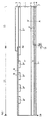
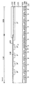
- Fig. 1 is a cross-sectional view illustrating the structure of the semiconductor device according to Embodiment 1.
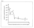
- Fig. 2 is a characteristic diagram illustrating an impurity concentration distribution along the cutting line A-A' of Fig. 1 .
- the horizontal axis indicates the distance from the rear surface of a substrate (an interface between an n + cathode layer 4 and a cathode electrode 7) in the depth direction of the substrate and the vertical axis indicates impurity concentration along the cutting line A-A' which traverses a rear-surface-side region of the substrate in the depth direction (which holds for Figs. 9 and 13 .
- Fig. 9 As illustrated in Fig.
- the semiconductor device includes an active region 10 and an edge termination structure portion (edge portion) 11 that surrounds the active region 10, which are provided in an n - semiconductor substrate that will be an n - drift region (first semiconductor region) 1.
- the active region 10 is a region in which a current flows when the semiconductor device is in an on state.
- the edge termination structure portion 11 has a function of reducing the electric field on the front surface side of the substrate and holding a breakdown voltage.
- a p + anode layer (second semiconductor region) 2 is provided in a surface layer of the front surface of the n - semiconductor substrate in the active region 10.
- a field limiting ring (FLR) 8 which is, for example, a floating p-type region is provided in the surface layer of the front surface in the edge termination structure portion 11.
- the lifetime ⁇ p of a minority carrier (hole) in the n - drift region 1 is controlled to be, for example, equal to or less than 10 ⁇ s (non-killer), preferably, equal to or greater than 0.1 ⁇ s and equal to or less than 3 ⁇ s.
- An interlayer insulating film 9 covers the front surface of the n - semiconductor substrate in the edge termination structure portion 11.
- An inner circumferential end portion of the interlayer insulating film 9 extends onto the surface of the p + anode layer 2.
- An anode electrode (first electrode) 3 is provided on the surface of the p + anode layer 2.
- An end portion of the anode electrode 3 extends onto the interlayer insulating film 9.
- the n + cathode layer (third semiconductor region) 4 is provided on a surface layer of the rear surface of the n - semiconductor substrate so as to extend from the active region 10 to the edge termination structure portion 11.
- the cathode electrode (second electrode) 7 is provided on the entire rear surface of the n - semiconductor substrate, that is, the entire surface of the n + cathode layer 4.
- An n buffer layer (fifth semiconductor region) 5 is provided in a portion of the n - drift region 1 close to the n + cathode layer 4 so as to extend from the active region 10 to the edge termination structure portion 11.
- the n buffer layer 5 has a function of preventing a depletion layer, which is spread from a pn junction between the p + anode layer 2 and the n - drift region 1 when the semiconductor device is turned off, from reaching the n + cathode layer 4.
- the n buffer layer 5 does not have this function, it may come into contact with the n + cathode layer 4 or it may be separated from the n + cathode layer 4.
- a floating buried p layer (fourth semiconductor region) 6 is provided at a position that is deeper than the n + cathode layer 4 from the rear surface of the substrate.
- the buried p layer 6 is uniformly provided in a predetermined range of the active region 10 which comes into contact with the n + cathode layer 4.
- the buried p layer 6 is provided in the surface layer of the n buffer layer 5 close to the n + cathode layer 4.
- the impurity concentration of the buried p layer 6 is higher than the impurity concentration of the n buffer layer 5 and is lower than the impurity concentration of the n + cathode layer 4.
- the impurity concentration of the buried p layer 6 may be, for example, equal to or greater than about 1 ⁇ 10 16 /cm 3 and equal to or less than about 10 ⁇ 10 19 /cm 3 and preferably equal to or greater than about 1 ⁇ 10 17 /cm 3 and equal to or less than about 1 ⁇ 10 18 /cm 3 .
- the impurity concentration of the buried p layer 6 is within the above-mentioned range, it is possible to prevent an increase in leakage current.
- An end portion 6a of the buried p layer 6 is located inside the side surface 1a of the n - semiconductor substrate (in the active region 10). That is, the end portion 6a of the buried p layer 6 does not reach the side surface 1a (chip side surface) of the n - semiconductor substrate. As such, when the end portion 6a of the buried p layer 6 is located inside the side surface 1a of the n - semiconductor substrate, snapback does not occur (snapback voltage ⁇ 0 V) and it is possible to prevent a jump in the current-voltage waveform (I-V waveform). The jump in the I-V waveform will be described below.
- the end portion 6a of the buried p layer 6 is located inside the end portion of the n + cathode layer 4. In this way, it is possible to prevent a short circuit due to the contact between the buried p layer 6 and the cathode electrode 7.
- the avalanche breakdown voltage (the voltage at which avalanche breakdown occurs) of the edge termination structure portion 11 can be greater than the avalanche breakdown voltage of the active region 10, as compared to the structure in which the buried p layer 6 is provided over the entire active region 10 and the entire edge termination structure portion 11.
- the reason is as follows. In the active region 10, when a reverse voltage is applied, holes are generated due to the avalanche breakdown which occurs in the pn junction between the buried p layer 6 and the n + cathode layer 4 and a hole current flows to the p + anode layer 2 through the n - drift region 1.
- the hole current becomes a base current in a parasitic pnp transistor including the p + anode layer 2, the n - drift region 1, and the buried p layer 6 and the parasitic pnp transistor operates. As a result, the avalanche breakdown voltage of the active region 10 is reduced.
- the avalanche breakdown voltage of the edge termination structure portion 11 can be calculated as follows. For example, a known device simulation is performed to calculate the breakdown voltage in the structure in which the edge termination structure portion is connected to the active region with a simple p-i-n (p-intrinsic-n) structure including a p + anode layer, an n - drift region, and an n + cathode layer. The calculated value may be used as the avalanche breakdown voltage of the edge termination structure portion 11. In this way, the avalanche breakdown voltage of the active region 10 can be less than the avalanche breakdown voltage of the edge termination structure portion 11. Therefore, an avalanche current can flow to the entire active region 10. As a result, it is possible to prevent the concentration of a current on the edge termination structure portion 11.
- the buried p layer 6 is not provided over the entire active region 10 and the entire edge termination structure portion 11, it is possible to reduce the number of electrons injected into an inactive region (for example, the edge termination structure portion 11) during reverse recovery. Therefore, it is possible to prevent the concentration of a current on an outer circumferential portion of the active region 10, that is, an end portion 3a of an anode contact due to the migration of the carriers, which are spread to the edge termination structure portion 11, to the anode electrode 3 through the anode contact during reverse recovery.
- the end portion 6a of the buried p layer 6 be disposed at a position that is a first length t1 inside from the end portion 3a of the anode contact (a junction between the p + anode layer 2 and the anode electrode 3) of the active region 10 (a position close to a central portion of an FWD cell).
- the FWD cell is a unit region including the p + anode layer 2, the n + cathode layer 4, the n buffer layer 5, and the buried p layer 6.
- the first length t1 from the end portion 3a of the anode contact to the end portion 6a of the buried p layer 6 which is disposed inside the end portion 3a may be equal to or less than a diffusion length L h of the minority carrier (t1 ⁇ L h ).
- L h the minority carrier
- the diffusion length L h of the minority carrier is represented by the following Expression (1).
- the lifetime of the minority carrier is ⁇ h and a diffusion coefficient of the minority carrier is D h .
- the diffusion coefficient D h of the minority carrier is represented by the following Expression (2).
- an elementary charge is q
- a Boltzmann constant is K
- an absolute temperature is T
- the mobility of the minority carrier is ⁇ h .
- KT/q is a thermal voltage at an absolute temperature T of 300 K.
- the diffusion coefficient D h of the minority carrier is 1.56 ⁇ 10 -3 cm 2 /s
- the mobility ⁇ h of the minority carrier is 0.06 cm 2 /Vs
- KT/q is 2.60 ⁇ 10 2 eV. Therefore, when the lifetime ⁇ h of the minority carrier in the n - drift region 1 is 10 ⁇ s (that is, when the minority carrier is a non-killer), the diffusion length L h of the minority carrier is 124.90 ⁇ m from the above-mentioned Expressions (1) and (2).
- the diffusion length L h of the minority carrier is 68.41 ⁇ m.
- lifetime ⁇ h of the minority carrier in the n - drift region 1 is 0.1 ⁇ s
- the diffusion length L h of the minority carrier is 12.49 ⁇ m.
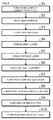
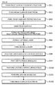
- Fig. 3 is a flowchart illustrating the outline of the method for manufacturing the semiconductor device according to Embodiment 1.
- a front surface element structure such as the p + anode layer 2 or the FLR 8 is formed on the front surface side of the n - semiconductor substrate which will be the n - drift region 1 (Step S1).
- a resist mask in which a region for forming the p + anode layer 2 and the FLR 8 is opened is formed on the front surface of the n - semiconductor substrate.
- p-type impurity ions such as boron (B) ions, are implanted into the front surface of the n - semiconductor substrate, using the resist mask as a mask.
- the implanted p-type impurities are thermally diffused to form the p + anode layer 2 and the FLR 8.
- the interlayer insulating film 9 is formed on the front surface of the n - semiconductor substrate.
- a portion of the interlayer insulating film 9 corresponding to the active region 10 is removed to form an anode contact hole through which the p + anode layer 2 is exposed.
- the front surface element structure is formed on the front surface side of the n - semiconductor substrate.
- the rear surface of the n - semiconductor substrate is ground to reduce the thickness of the n - semiconductor substrate (Step S2).
- n-type impurity ions such as selenium (Se) ions
- n buffer layer 5 n-type impurity ions
- a resist mask in which a region for forming the buried p layer 6 is opened is formed on the rear surface of the n - semiconductor substrate.
- the resist mask covers the edge termination structure portion 11 and a portion of the active region 10 which is the first length t1 inside from the end portion of the anode contact hole.
- p-type impurity ions such as boron ions
- boron ions are implanted into the rear surface of the n - semiconductor substrate, using the resist mask as a mask, to form the buried p layer 6 in the active region 10 (Step S4).
- the p-type impurity concentration of the rear surface of the n - semiconductor substrate by ion implantation in Step S5 may be, for example, equal to or less than 1 ⁇ 10 15 /cm 3 .
- the n + cathode layer 4 formed in Step S5 does not have a uniform thickness, it is possible to prevent a short circuit between the buried p layer 6 and the cathode electrode 7 in a thin portion of the n + cathode layer 4. That is, it is preferable that the surface layer of the rear surface of the n - semiconductor substrate after the ion implantation in Step S5 have an impurity concentration distribution close to that of the n-type region.
- n-type impurity ions such as phosphorus (P) ions
- P phosphorus
- the impurities implanted in the ion implantation process of Steps S3 to S5 are collectively thermally diffused by a heat treatment using, for example, furnace annealing (Step S6). Since the impurities implanted in the ion implantation process of Steps S3 to S5 are collectively thermally diffused, it is possible to reduce the number of processes and to reduce costs.
- Steps S3 to S5 it is preferable to thermally diffuse the implanted impurities.
- the order of the ion implantation process of Steps S3 to S5 may be changed in various ways.
- the anode electrode (front surface electrode) 3 is formed on the front surface of the n - semiconductor substrate so as to be buried in the anode contact hole and is patterned in a predetermined shape (Step S7).
- a passivation film (not illustrated) is formed on the front surface of the n - semiconductor substrate and is patterned in a predetermined shape (Step S8).
- electron beams are radiated to the n - semiconductor substrate to control the lifetime of the carriers in the n - drift region 1 (Step S9).
- the cathode electrode 7 is formed on the rear surface of the n - semiconductor substrate (Step S10). In this way, the FWD illustrated in Fig. 1 is completed.
- FIG. 4 is a diagram illustrating the operation of a semiconductor device according to a comparative example when a forward voltage is applied.
- Fig. 5 is a diagram illustrating the operation of the semiconductor device according to Embodiment 1 when the forward voltage is applied.
- Fig. 4 illustrates an FWD (hereinafter, referred to as a comparative example) with a structure in which an end portion 126a of a buried p layer 126 reaches a side surface 121a of an n - semiconductor substrate.
- Fig. 5 illustrates the FWD according to Embodiment 1 illustrated in Fig. 1 .
- the edge termination structure portion 11 is shortened and the n buffer layer 5 is not illustrated, in order to clearly describe the operation of the carriers.
- this is substantially the same as a state in which a short circuit occurs between the buried p layer 126-1 and the cathode electrode 127 in the side surface 121a of the n - semiconductor substrate. Therefore, no electron is injected from the n + cathode layer 124 to the n - drift region 121 and the FWD is not turned on.
- Fig. 4(a) illustrates a first comparative example in which the rear surface of a chip is soldered to, for example, a direct copper bond (DCB) substrate.
- DCB direct copper bond
- a solder layer 128 on the rear surface of the chip protrudes from the side surface of the chip (the side surface 121a of the n - semiconductor substrate) and the end portion 126a of the buried p layer 126-1 is short-circuited to the cathode electrode 127 by the solder layer 128 (a portion represented by reference numeral 120).
- the state in which the solder layer 128 reaches the side surface 121a of the n - semiconductor substrate indicates, for example, a state in which, when the n - semiconductor substrate is incorporated into a power module and is soldered to the DCB substrate, the solder layer 128 which is melted in the rear surface of the n - semiconductor substrate flows from the rear surface to the side surface 121a of the n - semiconductor substrate and comes into contact with the side surface 121a.
- the depth of a junction interface between the n + cathode layer 124 and the buried p layer 126-1 in the rear surface of the n - semiconductor substrate is about 1 ⁇ m to 3 ⁇ m from the rear surface of the n - semiconductor substrate. Therefore, when the solder layer 128 with a thickness of 300 ⁇ m or more protrudes from the side surface 121a of the n - semiconductor substrate, a short circuit is likely to occur between the buried p layer 126-1 and the cathode electrode 127 in the side surface 121a of the n - semiconductor substrate.
- the first comparative example has undesirable characteristics that, after the forward voltage is applied, there is a period for which the FWD does not operate (a jump in the I-V waveform) and the FWD starts to operate after the period has elapsed.
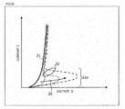
- Fig. 30 illustrates an I-V waveform when a diode is biased forward.
- Fig. 30 is a characteristic diagram illustrating the current-voltage waveform when the diode is biased forward. As represented by a thick solid line, in a general waveform (hereinafter, referred to as a normal waveform) 21, a current increases with a forward voltage drop.
- a high forward voltage drop occurs and little current flows, as represented by a dotted line (a waveform represented by reference numeral 22). Therefore, at the time when the voltage drop between the buried p layer and the n cathode layer is equal to or greater than the built-in voltage due to the passage of holes, a current flows at once and the forward voltage drop of the diode is reduced. A region which serves as negative resistance is snapback, that is, a jump 22a in the I-V waveform.
- the resistance R12 of the short pass in the buried p ++ layer 126-2 decreases and a voltage (snapback voltage) which causes the snapback increases. Therefore, the jump in the I-V waveform increases.
- the magnitude of the impurity concentration of the buried p layer is represented by the direction of an arrow 20.
- the jump 22a increases as the impurity concentration of the p layer increases (an I-V waveform 22 indicated by a dashed line).
- the I-V waveform 22 with the smallest jump 22a which is represented by the thinnest dotted line corresponds to the first comparative example illustrated in Fig. 4(a) and the other I-V waveforms 22 correspond to the second comparative example illustrated in Fig. 4(b) .
- reference numeral 122 indicates a p + anode layer and reference numeral 123 indicates an anode electrode.
- the end portion 6a of the buried p layer 6 does not reach the side surface 1a of the n - semiconductor substrate and the buried p layer 6 is in a floating state.
- resistance R10 between the end portion 6a of the buried p layer 6 and the side surface 1a of the n - semiconductor substrate is determined by the impurity concentration of the n - drift region 1 with high resistance and is more than the resistance R11 and the resistance R12 of the first and second comparative examples which are determined by the impurity concentration of the buried p layers 126-1 and 126-2.
- the holes which are injected from the p + anode layer 2 to the buried p layer 6 through the n - drift region 1 when the forward voltage is applied is less likely to move from the end portion 6a of the buried p layer 6 to the cathode electrode 7 on the side surface 1a of the n - semiconductor substrate (a portion represented by reference numeral 12) and moves to the n + cathode layer 4.
- electrons are injected from the n + cathode layer 4 to the n - drift region 1. Therefore, in the semiconductor device according to the invention, a jump in the I-V waveform does not occur.
- the semiconductor device according to the invention has the normal waveform 21 illustrated in Fig. 30 and operates substantially similarly to the general FWD without the buried p layer 6.
- Reference numeral 28 indicates a solder layer when the rear surface of the chip is soldered to, for example, the DCB substrate.
- Embodiment 1 since the buried p layer is uniformly provided, a uniform voltage drop (avalanche breakdown) can occur in the rear surface of the substrate during reverse recovery and it is possible to prevent a jump in the I-V waveform. Therefore, it is possible to perform soft recovery and to avoid problems due to EMI noise.
- the buried p layer since the buried p layer is uniformly provided, alignment accuracy in the rear surface of the substrate does not need to be higher than that in the structure according to the related art in which a plurality of buried p layers are provided at predetermined intervals. Therefore, it is possible to form the buried p layer with high dimensional accuracy with a small number of processes. In addition, special equipment for improving alignment accuracy is not needed. Therefore, it is possible to provide a semiconductor device at low costs.
- the breakdown voltage of the active region is less than the breakdown voltage of an inactive region. Therefore, it is possible to prevent the concentration of the electric field on the end portion of the active region during reverse recovery.
- the reason is as follows.
- the pn junction hereinafter, referred to as a pn junction J1 between the buried p layer and the n cathode layer on the rear surface of the substrate is reversely biased.
- the impurity concentration of the two layers is higher than the impurity concentration of the semiconductor substrate by two digits or more.
- a voltage of 100 V or less is applied to the pn junction J1, avalanche breakdown is easy to occur.
- the pn junction J1 causes the avalanche breakdown, holes are injected from the pn junction J1 in which the buried p layer is formed. The holes drift to the p + anode layer in the depletion layer. Then, electric field intensity is increased by the holes even in the vicinity of a pn junction (hereinafter, referred to as a pn junction J2) between the p + anode layer and the n drift layer. That is, the gradient of electric field intensity increases in the vicinity of the pn junction J2 due to an excessive increase in positive charge caused by the holes according to the Poisson's equation.
- the effective impurity concentration of the semiconductor substrate increases.
- the maximum electric field intensity of the pn junction J2 significantly increases and reaches critical electric field intensity.
- avalanche breakdown occurs.
- a dynamic breakdown voltage is reduced in the active region. Since the increase in the maximum electric field intensity of the pn junction J2 occurs only in the active region in which the buried p layer is formed, the dynamic breakdown voltage is not reduced in the inactive region. This is the reason why the dynamic breakdown voltage is reduced in the active region and the inactive region.
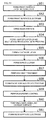
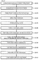
- Fig. 6 is a flowchart illustrating the outline of the semiconductor device manufacturing method according to Embodiment 2.
- the semiconductor device manufacturing method according to Embodiment 2 differs from the semiconductor device manufacturing method according to Embodiment 1 in that, after electron beams are radiated to control the lifetime, an n + cathode layer 4 is formed and laser annealing is performed to activate the n + cathode layer 4.
- Step S11 to S14 a process from the formation of a front surface element structure to the formation of a buried p layer 6 is performed. Then, after a resist mask used to form the buried p layer 6 is removed, impurities which are implanted by an ion implantation process for forming an n buffer layer 5 and an ion implantation process for forming the buried p layer 6 are thermally diffused by a heat treatment using, for example, furnace annealing (Step S15). Then, similarly to Embodiment 1, a process from the formation of an anode electrode 3 to the control of the lifetime is performed (Steps S16 to S18).
- the n + cathode layer 4 is formed on the entire rear surface of the n - semiconductor substrate (Step S19).
- a method for forming the n + cathode layer 4 is the same as that in Embodiment 1.
- laser annealing is performed on the rear surface of the n - semiconductor substrate to activate the n + cathode layer 4 (Step S20).
- a cathode electrode 7 is formed on the rear surface of the n - semiconductor substrate (Step S21). In this way, the FWD illustrated in Fig. 1 is completed.
- Embodiment 2 it is possible to obtain the same effect as that in Embodiment 1.
- FIG. 7 is a flowchart illustrating the outline of the semiconductor device manufacturing method according to Embodiment 3.
- the semiconductor device manufacturing method according to Embodiment 3 differs from the semiconductor device manufacturing method according to Embodiment 2 in that an anode electrode 3 is formed on the front surface of an n - semiconductor substrate before the rear surface of the n - semiconductor substrate is ground to reduce the thickness of the n - semiconductor substrate.
- a front surface element structure is formed on the front surface of the n - semiconductor substrate which will be an n - drift region 1 (Step S31) and the anode electrode 3 is formed (Step S32).
- a method for forming the front surface element structure and a method for forming the anode electrode 3 are the same as those in Embodiment 1.
- a process from the grinding of the rear surface of the n - semiconductor substrate to a heat treatment is performed (Steps S33 to S36).
- a process from the formation of a passivation film to the formation of a cathode electrode 7 is performed (Steps S37 to S41). In this way, the FWD illustrated in Fig. 1 is completed.
- Embodiment 3 it is possible to obtain the same effect as that in Embodiments 1 and 2.
- Fig. 8 is a cross-sectional view illustrating the structure of the semiconductor device according to Embodiment 4.
- Fig. 9 is a characteristic diagram illustrating an impurity concentration distribution along a cutting line B-B' of Fig. 8 .
- the semiconductor device according to Embodiment 4 differs from the semiconductor device according to Embodiment 1 in that a plurality of n buffer layer 15 are formed at different depths from the rear surface of a substrate by multi-stage irradiation with protons from the rear surface of the substrate.
- an n buffer layer 15a is arranged at the deepest position from the rear surface of an n - semiconductor substrate which will be an n - drift region 1.
- an n buffer layer 15b is arranged at a position that is shallower than the n buffer layer 15a from the rear surface of the n - semiconductor substrate so as to be separated from the n buffer layer 15a.
- an n buffer layer 15c is arranged at a position that is shallower than the n buffer layer 15b from the rear surface of the n - semiconductor substrate so as to be separated from the n buffer layer 15b. That is, the n - drift region 1 is arranged between the n buffer layers 15a to 15c.
- the n buffer layer 15c is arranged at a position that is deeper than the n + cathode layer 4 and a buried p layer 6 is provided between the n buffer layer 15c and an n + cathode layer 4 in an active region 10.
- the n buffer layer 15c may come into contact with the buried p layer 6 or it may be separated from the buried p layer 6.
- Fig. 10 is a flowchart illustrating the outline of the semiconductor device manufacturing method according to Embodiment 4.
- a front surface element structure is formed on the front surface side of the n - semiconductor substrate which will be the n - drift region 1 (Step S51) and the anode electrode 3 is formed (Step S52).
- a method for forming the front surface element structure and a method for manufacturing the anode electrode 3 are the same as those in Embodiment 1.
- the rear surface of the n - semiconductor substrate is ground to reduce the thickness of the n - semiconductor substrate (Step S53).
- Step S54 three proton irradiation processes are performed in different ranges from the rear surface of the n - semiconductor substrate to form the n buffer layers 15a to 15c at different depths from the rear surface of the substrate.
- n-type impurity ions such as phosphorus ions
- Step S55 n-type impurity ions
- Step S56 the buried p layer 6 is formed at the position that is deeper than the n + cathode layer 4 and is shallower than the n buffer layer 15c from the rear surface of the substrate.
- a method for forming the n + cathode layer 4 and a method for forming the buried p layer 6 are the same as those in Embodiment 1.
- Step S57 a heat treatment is performed to collectively activate and thermally diffuse the protons and the impurities which are implanted in Steps S54 to S56 (Step S57).
- a passivation film is formed on the front surface of the n - semiconductor substrate (Step S58) and the lifetime of the carriers in the n - drift region 1 is controlled (Step S59).
- a method for forming the passivation film and a method for controlling the lifetime are the same as those in Embodiment 1.
- laser annealing is performed on the rear surface of the n - semiconductor substrate to activate the n + cathode layer 4 (Step S60).
- a cathode electrode 7 is formed on the rear surface of the n - semiconductor substrate (Step S61). In this way, the FWD illustrated in Fig. 8 is completed.
- Embodiment 4 it is possible to obtain the same effect as that in Embodiments 1 to 3.
- Fig. 11 is a cross-sectional view illustrating the structure of the semiconductor device according to Embodiment 5.
- An impurity concentration distribution along a cutting line A-A' of Fig. 11 is the same as the impurity concentration distribution illustrated in Fig. 2 .
- the semiconductor device according to Embodiment 5 differs from the semiconductor device according to Embodiment 1 is that an end portion 14a of an n + cathode layer 14 is located inside a side surface 1a of an n - semiconductor substrate (on the side close to the center of an FWD cell).
- the n + cathode layer 14 is not provided on the rear surface side of the substrate in an edge termination structure portion 11 and a Schottky junction between a cathode electrode 7 and an n buffer layer 5 is formed on the rear surface side of the substrate.
- An end portion 6a of a buried p layer 6 is preferably provided at a position that is a second length t2 inside from the end portion 14a of the n + cathode layer 14.
- the second length t2 has allowance for alignment accuracy (for example, allowance that is about two times the alignment accuracy).
- the second length t2 is preferably equal to or greater than about 1 ⁇ m and equal to or less than about 10 ⁇ m.
- the second length t2 from the end portion 6a of the buried p layer 6 to the end portion 14a of the n + cathode layer 14 is preferably, for example, equal to or greater than about 1 ⁇ m and equal to or less than about 10 ⁇ m.
- a resist mask in which a region for forming the n + cathode layer 14 is opened may be formed on the rear surface of the n - semiconductor substrate and the n + cathode layer 14 may be formed in an active region 10, using the resist mask as a mask in Step S5 which is the same as that in the semiconductor device manufacturing method according to Embodiment 1.
- the semiconductor device manufacturing method according to Embodiment 5 is the same as the semiconductor device manufacturing method according to Embodiment 1 except for the step of forming the n + cathode layer 14.
- Embodiment 5 it is possible to obtain the same effect as that in Embodiments 1 to 4.
- the n + cathode layer is not provided in the edge termination structure portion and the Schottky junction between the n + cathode layer and the cathode electrode is formed in the edge termination structure portion. Therefore, when the forward voltage is applied, the injection of the carriers (electrons) from the cathode in the edge termination structure portion is further suppressed. Therefore, it is possible to prevent the carriers from being stored in the edge termination structure portion and thus to prevent the concentration of a current on the end portion of the anode contact during reverse recovery. As a result, it is possible to improve the breakdown voltage during reverse recovery.
- Fig. 12 is a cross-sectional view illustrating the structure of the semiconductor device according to Embodiment 6.
- Fig. 13 is a characteristic diagram illustrating an impurity concentration distribution along the cutting line C-C' of Fig. 12 .
- the impurity concentration distribution along the cutting line A-A' of Fig. 12 is the same as the impurity concentration distribution illustrated in Fig. 2 .
- the semiconductor device according to Embodiment 6 differs from the semiconductor device according to Embodiment 5 in that a p - region (sixth semiconductor region) 16 is provided in an n buffer layer 5 in an edge termination structure portion 11 so as to come into contact with a cathode electrode 7, thereby forming a Schottky junction between the p - region 16 and the cathode electrode 7.
- An outer circumferential end portion 16a of the p - region 16 extends to a side surface 1a of an n - semiconductor substrate.
- the impurity concentration of the p - region 16 may be equal to the impurity concentration of a buried p layer 6.
- a distance between an end portion 6a of the buried p layer 6 and the inner circumferential end portion 16b of the p - region 16 is a third length t3. According to this structure, since a potential difference occurs between the buried p layer 6 and the p - region 16, it is possible to prevent a jump in the I-V waveform, similarly to Embodiment 1.
- the third length t3 between the end portion 6a of the buried p layer 6 and the inner circumferential end portion 16b of the p - region 16 is preferably equal to or greater than the width Xn of a built-in depletion layer at the pn junction between the n buffer layer 5 and the buried p layer 6, and equal to or less than the diffusion length L h of the minority carrier.
- the reason why the third length t3 is set to be equal to or less than the diffusion length L h of the minority carrier is to prevent a reduction in the effect obtained by the formation of the p - region 16.
- the reason why the third length t3 is set to be equal to or greater than the width Xn of the built-in depletion layer at the pn junction between the n buffer layer 5 and the buried p layer 6 is as follows. In a thermal equilibrium state in which the forward voltage is not applied, the depletion layer (built-in depletion layer) is formed at the pn junction between the n buffer layer 5 and the buried p layer 6 in the n buffer layer 5.
- the depletion layer which is spread from the pn junction between the n buffer layer 5 and the buried p layer 6 reaches the p - region 16 due to the holes which are injected from the anode by the application of the forward voltage and a jump in the I-V waveform occurs.
- the width Xn of the built-in depletion layer at the pn junction between the n buffer layer 5 and the buried p layer 6 is represented by the following Expression (3).
- a built-in voltage ⁇ b of the pn junction between the n buffer layer 5 and the buried p layer 6 is represented by the following Expression (4).
- the donor concentration of the n buffer layer 5 is N D
- the acceptor concentration of the buried p layer 6 is N A
- an elementary charge is q
- a Boltzmann constant is K
- an absolute temperature is T
- intrinsic carrier concentration when the absolute temperature T is 300 K is n i
- vacuum permittivity is ⁇ 0
- the specific permittivity of silicon is ⁇ s .
- KT/q indicates a thermal voltage when the absolute temperature T is 300 K.
- the donor concentration N D of the n buffer layer 5 is 1.00 ⁇ 10 21 /cm 3
- the acceptor concentration N A of the buried p layer 6 is 1.00 ⁇ 10 23 /cm 3
- the intrinsic carrier concentration n i is 1.50 ⁇ 10 16 /cm 3
- KT/q is 2.60 ⁇ 10 2 eV
- the vacuum permittivity ⁇ 0 is 8.85 ⁇ 10 -12 F/cm
- the specific permittivity ⁇ s of silicon is 1.17x10 F/cm
- the elementary charge q is 1.60 ⁇ 10 19 C.
- the built-in voltage ⁇ b of the pn junction between the n buffer layer 5 and the buried p layer 6 is 6.87 ⁇ 10 -1 V.
- the width Xn of the built-in depletion layer at the pn junction between the n buffer layer 5 and the buried p layer 6 is 0.945 ⁇ m.
- Step S4 a resist mask in which a region for forming the n + cathode layer 14 is opened is formed on the rear surface of the n - semiconductor substrate and the n + cathode layer 14 is formed in the active region 10 using the resist mask as a mask in Step S5, unlike the semiconductor device manufacturing method according to Embodiment 1.
- Step S6 a resist mask in which a region for forming the p - region 16 is opened is formed and the p - region 16 is formed in the edge termination structure portion 11 using the resist mask as a mask. Then, in Step S6, the heat treatment is preferably performed to collectively activate the impurities implanted by an ion implantation process.
- the semiconductor device manufacturing method according to Embodiment 6 is the same as the semiconductor device manufacturing method according to Embodiment 1 except for the steps of forming the n + cathode layer 14 and the p - region 16.
- Embodiment 6 it is possible to obtain the same effect as that in Embodiments 1 to 5.
- the n + cathode layer is not provided in the edge termination structure portion and the junction between the p - region and the cathode electrode is formed in the edge termination structure portion. Therefore, it is possible to obtain the same effect as that in Embodiment 5.
- FIG. 14 is a cross-sectional view illustrating the structure of the semiconductor device according to Embodiment 7.
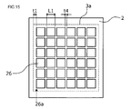
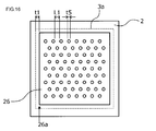
- Figs. 15 to 17 are plan views illustrating examples of the plane pattern of a buried p layer in a semiconductor device according to Embodiment 7.
- the position of an end portion 3a of an anode contact which is projected from the front surface of a substrate to an n + cathode layer 4 on the rear surface of the substrate is represented by a dotted line (which holds for Figs. 21 and 22 ).
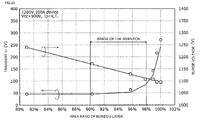
- the area ratio of the occupation area A11 of the surface area of the buried p layer 26 to the surface area A10 of the portion which is disposed inside the end portion 3a of the anode contact may be equal to or greater than 90% and equal to or less than 98% and preferably equal to or greater than 92% and equal to or less than 96%. In this case, it is possible to obtain a low transient V F (on-voltage) and soft recovery characteristics.
- the surface area A10 of the portion which is disposed inside the end portion 3a of the anode contact means the surface area of the active region 10.
- the occupation area A11 of the surface area of the buried p layer 26 means the total surface area of the buried p layer 26.
- An end portion 26a of the pattern of the buried p layer 26 which is closest to the edge termination structure portion 11 is preferably located at a position that is a first length t1 inside from the end portion 3a of the anode contact (toward the center of the FWD cell), similarly to Embodiment 1.
- the first length t1 is preferably, for example, about 50 ⁇ m corresponding to the diffusion length L h of the minority carrier.
- the plane pattern of the buried p layer 26 can vary depending on the design condition.
- the plane pattern of the buried p layer 26 has a stripe shape, a matrix shape in which substantial rectangles or substantial dots are regularly arranged at predetermined intervals (that is, a shape in which the buried p layer 26 is opened in a lattice shape: Fig. 15 ), a shape in which substantially rectangular openings or substantially circular openings are regularly arranged in a matrix at predetermined intervals in the buried p layer 26 ( Fig. 16 ), and a mosaic shape in which openings with an arbitrary shape are arranged in an arbitrary pattern.
- the plane pattern of the buried p layer 26 may be the same plane pattern as that in Embodiment 1.
- one buried p layer 26 with a substantially rectangular shape may be uniformly formed on the entire central portion of the active region 10 and a region in which the buried p layer 26 is not provided may be provided in a substantially rectangular frame shape around the buried p layer 26 in the active region 10.
- the width of the region, in which the buried p layer 26 is not provided, around the buried p layer 26 is preferably equal to the first length t1 which can obtain the above-mentioned area ratio.
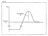
- Fig. 18 is a characteristic diagram illustrating the voltage waveform of the FWD. As illustrated in Fig.
- the drop of a forward voltage V F (a voltage V AK between the anode and the cathode) increases temporarily while the carriers are stored in the n - drift region 1 (for example, about a few tens of volts). Then, when the storage of the carriers is completed, the semiconductor device is in a steady state and the forward voltage V F is converged on a steady-state value (for example, about 1 V to 3 V).
- the forward voltage V F which transiently increases while the voltage changes from the reverse bias to the forward bias and the semiconductor is turned on is referred to as the transient forward voltage (hereinafter, referred to as a transient V F ).
- the transient V F When the transient V F is high, electrical loss occurs during the actual operation of a machine, such as an inverter, and an element temperature increases due to the electrical loss. Therefore, it is preferable that the transient V F be low. For this reason, when the buried p layer 26 is formed, a portion of the buried p layer 26 is removed to form an opening portion (hole). In this way, when the forward bias is applied, electrons are injected from the n + cathode layer 4 to the n - drift region 1 through the opening portion, without being blocked by the buried p layer 26. That is, the opening portion of the buried p layer 26 serves as the path of the electrons injected from the n + cathode layer 4 to the n - drift region 1.
- the planar shape of the opening portion in the buried p layer 26 may be, for example, a lattice shape with a width t4 in which substantial rectangles with a fourth length (width) L1 remain in a matrix as illustrated in Fig. 15 or a shape in which circles with a diameter t5 are regularly arranged in a matrix at an interval of the fourth length L1 as illustrated in Fig. 16 .
- the opening portion of the buried p layer 26 may have a substantially rectangular frame shape which surrounds the buried p layer 26. That is, this is equivalent to a structure in which the opening portion which serves as the path of the electrons injected from the n + cathode layer 4 to the n - drift region 1 is not formed in the buried p layer 26, but is formed around the buried p layer 26.
- the width (that is, the first length t1) of the opening portion of the buried p layer 26 may be greater than the diffusion length L h of the minority carrier or 50 ⁇ m.
- the holes which are injected from the p + anode layer 2 to the n - drift region 1 cause a voltage drop in the buried p layer 26, move in the buried p layer 26, and reaches the n + cathode layer 4 through the opening portion of the buried p layer 26.
- the voltage drop is greater than the built-in potential of the pn junction between the buried p layer 26 and the n + cathode layer 4, electrons are injected from the n + cathode layer 4 to the buried p layer 26.
- the opening portion which serves the path of the electrons injected from the n + cathode layer 4 to the n - drift region 1 is provided around the buried p layer 26 as illustrated in Fig. 17 , the sufficient length of the buried p layer 26 in the direction horizontal to the rear surface of the substrate is maintained. Therefore, when the opening portion which serves the path of the electrons injected from the n + cathode layer 4 to the n - drift region 1 is provided around the buried p layer 26 as illustrated in Fig. 17 , it is easy to prevent an increase in the transient V F or a jump in the I-V waveform, as compared to the structure in which the opening portion is selectively provided in the buried p layer 26.
- the opening portion which serves the path of the electrons injected from the n + cathode layer 4 to the n - drift region 1 is provided around the buried p layer 26 as illustrated in Fig. 17 , when the ratio of the total surface area of the buried p layer 26 to the surface area A10 of the portion which is disposed inside the end portion 3a of the anode contact is equal to or greater than 50%, the soft recovery effect is sufficiently obtained during reverse recovery.
- the distance (that is, the first length t1) between the projected position of the end portion 3a of the anode contact on the rear surface of the substrate and the end portion 26a of the buried p layer 26 is preferably set to a value at which the area ratio of the occupation area A11 of the surface area of the buried p layer 26 is equal to or greater than 50%.
- the distance is preferably equal to or less than 2000 ⁇ m.
- the length (fourth length) L1 of the buried p layer 26 in the direction horizontal to the rear surface of the substrate depends on the impurity concentration of the buried p layer 26 and can be calculated, for example, as follows.
- current density is J
- an elementary charge is q
- hole mobility is ⁇
- the thickness of the buried p layer 26 is d
- the impurity concentration of the buried p layer 26 is Np
- the built-in potential of the pn junction between the buried p layer 26 and the n + cathode layer 4 is Vbi
- the length L1 of the buried p layer 26 in the direction horizontal to the rear surface of the substrate satisfies the following Expression (5).
- the length L1 of the buried p layer 26 in the direction horizontal to the rear surface of the substrate is about 250 ⁇ m from the above-mentioned Expression (5).
- the length L1 of the buried p layer 26 in the direction horizontal to the rear surface of the substrate is equal to or greater than 250 ⁇ m, it is possible to reduce the transient V F .
- the length L1 of the buried p layer 26 in the direction horizontal to the rear surface of the substrate may satisfy the following Expression (6).
- the semiconductor device manufacturing method according to Embodiment 7 differs from the semiconductor device manufacturing method according to Embodiment 1 in that, when the buried p layer 26 is formed, a mask in which the plane pattern of the buried p layer 26 is formed is used as an ion implantation mask. Specifically, first, a process from the formation of the front surface element structure to the formation of an n buffer layer 5 is performed, similarly to Steps S1 to S3 in Embodiment 1. Then, the n + cathode layer 4 is formed on the rear surface of an n - semiconductor substrate. A method for forming the n + cathode layer 4 is the same as that in Embodiment 1.
- a resist mask in which a region for forming the buried p layer 26 is opened is formed on the rear surface of the n - semiconductor substrate by photolithography.
- the resist mask covers, for example, the edge termination structure portion 11 and a portion of the active region 10 that is the first length t1 inside from the end portion of the anode contact hole.
- the pattern of the buried p layer 26 is formed in a portion of the resist mask which is disposed inside the end portion of the anode contact hole.
- p-type impurity ions such as boron ions, are implanted into the rear surface of the n - semiconductor substrate, using the resist mask as a mask, to form the buried p layer 26.
- n + cathode layer 4, the n buffer layer 5, and the buried p layer 26 can be changed in various ways. Similarly to Embodiment 1, the n buffer layer 5, the buried p layer 26, and the n + cathode layer 4 may be formed in this order. Then, similarly to Step S6 in Embodiment 1, thermal diffusion is collectively performed on the impurities which are implanted by the ion implantation process. Instead of the collective heat treatment, whenever impurities are implanted by the ion implantation process, thermal diffusion may be performed on the implanted impurities. Then, a process from the formation of an anode electrode 3 to the formation of a cathode electrode 7 is performed similarly to Steps S7 to S10 in Embodiment 1. In this way, the FWD illustrated in Fig. 14 is completed.
- Embodiment 7 it is possible to obtain the same effect as that in Embodiments 1 to 6.
- the buried p layer 26 is provided inside the end portion 3a of the anode contact at a predetermined area ratio and the area ratio of the buried p layer is optimized. Therefore, it is possible to provide a semiconductor device which has soft recovery characteristics and a low transient V F .
- the conductivity modulation of the pnpn structure portion is delayed, a high transient on-voltage is generated when the FWD is turned on. As a result, the switching loss of the FWD increases and the surge voltage increases when the IGBT of the opposite arm is turned off.
- Fig. 19 is a cross-sectional view illustrating the structure of the semiconductor device according to Embodiment 8.
- the semiconductor device according to Embodiment 8 differs from the semiconductor device according to Embodiment 7 in that a plurality of n buffer layers 15 which have different depths from the rear surface of a substrate are formed by multi-stage irradiation with protons from the rear surface of the substrate.
- An n buffer layer 15 has the same structure as that in Embodiment 4. That is, for example, when the n buffer layer 15 is formed by three-stage irradiation with protons, the n buffer layer 15 includes n buffer layers 15a to 15c in ascending order of depth from the rear surface of an n - semiconductor substrate.
- a method for manufacturing the semiconductor device according to Embodiment 8 differs from the semiconductor device manufacturing method according to Embodiment 4 in that, when a buried p layer 26 is formed, an ion implantation mask in which the plane pattern of the buried p layer 26 is formed in a portion that is disposed inside an end portion of an anode contact hole is used, similarly to Embodiment 7.
- the semiconductor device manufacturing method according to Embodiment 8 is the same as the semiconductor device manufacturing method according to Embodiment 4 except for a step of forming the buried p layer 26.
- Embodiment 8 it is possible to obtain the same effect as that in Embodiments 1 to 7.
- Fig. 20 is a cross-sectional view illustrating the structure of the semiconductor device according to Embodiment 9.
- Fig. 21 is a plan view illustrating an example of the plane pattern of a buried p layer illustrated in Fig. 20 .
- Fig. 21 illustrates an example in which buried p layer (hereinafter, referred to as first and second buried p layers) 26 and 36 are regularly arranged in a matrix at predetermined intervals.
- first and second buried p layers buried p layer
- the area ratio of the occupation area A21 of the surface area of the second buried p layer 36 in the edge termination structure portion 11 to the surface area A20 of the portion which is disposed outside the end portion 3a of the anode contact is greater than the area ratio of the occupation area A11 of the surface area of the first buried p layer 26 to the surface area A10 of a portion which is disposed inside the end portion 3a of the anode contact. Therefore, when dynamic avalanche occurs, the breakdown voltage of the edge termination structure portion 11 is greater than the breakdown voltage of an active region 10. As a result, the breakdown voltage of the active region 10 is a standard in an avalanche during reverse recovery. Therefore, it is possible to avoid the concentration of a current on the end portion 3a of the anode contact during reverse recovery and to improve the breakdown voltage.
- the second buried p layer 36 is arranged in the range from the vicinity of the boundary between the end portion 3a (active region 10) of the rectangular anode contact and the edge termination structure portion 11 to the edge termination structure portion 11 so as to be laid across the end portion 3a of the anode contact.
- the width t6 of an opening portion in the second buried p layer 36 is greater than that in the first buried p layer 26 which is disposed inside the end portion 3a and the anode contact and the length L2 of the second buried p layer 36 in a direction horizontal to the rear surface of the substrate is less than that in the first buried p layer 26 (t6 > t4 and L2 ⁇ L1).
- the first buried p layer 26 has the same structure as that in Embodiment 7. As such, since the second buried p layer 36 is provided in the edge termination structure portion 11, it is possible to further reduce the transient V F and to further improve soft recovery characteristics.
- Embodiment 9 it is possible to obtain the same effect as that in Embodiments 1 to 8.
- Fig. 22 is a plan view illustrating the structure of the semiconductor device according to Embodiment 10.
- Fig. 22 illustrates an example of the plane pattern of a buried p layer.
- the semiconductor device according to Embodiment 10 differs from the semiconductor device according to Embodiment 1 in that second buried p layers 46 are provided at four corners of an end portion 3a of a rectangular anode contact so as to be laid across the vicinity of the boundary between the end portion 3a of the anode contact and an edge termination structure portion 11.
- the second buried p layer 46 comes into contact with a buried p layer (hereinafter, referred to as a first buried p layer) 6 which is disposed inside the end portion 3a of the anode contact.
- a first buried p layer hereinafter, referred to as a first buried p layer
- Embodiment 10 when dynamic avalanche occurs, the breakdown voltage of the edge termination structure portion 11 is reduced at the corners of the end portion 3a of the anode contact. However, when the forward bias is applied, conductivity modulation is less likely to occur at the corners of the end portion 3a of the anode contact.
- the holes which are injected from a p + anode layer 2 to an n - drift region 1 when dynamic avalanche occurs flows to a contact surface of an anode electrode 3 which is surrounded by the end portion 3a of the anode contact according to electrostatic potential. The number of carriers stored in the edge termination structure portion 11 is reduced at the corners of the end portion 3a of the anode contact.
- the concentration of a current on the corners of the end portion 3a of the anode contact is reduced.
- the concentration of a current on the corners of the end portion 3a of the anode contact is also reduced.
- Embodiment 10 it is possible to obtain the same effect as that in Embodiments 1 to 9.
- Fig. 23 is a characteristic diagram illustrating the relationship among a transient forward voltage, a surge voltage during reverse recovery, and the area ratio of a buried p layer in a semiconductor device according to Example 1.
- An FWD (hereinafter, referred to as Example 1) in which the area ratio of a buried p layer was changed to various values was manufactured by the semiconductor device manufacturing method according to Embodiment 7 and the transient V F (on-voltage) and the surge voltage during the reverse recovery were measured.
- Fig. 23 illustrates the measurement results.
- a breakdown voltage was 1200 V
- a rated current was 100 A
- a power supply voltage Vcc was 900 V
- a junction (pn junction) temperature Tj was the room temperature (for example, 25°C).
- the transient V F When the transient V F is equal to or less than 100 V and the surge voltage is equal to or less than 1170 V, it is possible to achieve a low transient V F and soft recovery.
- the reason why the transient V F is set to 100 V or less is that, when the transient V F is greater than 100 V, electrical loss increases during the operation of an inverter.
- the reason why the surge voltage is set to 1170 V or less is to reduce damage due to an electrical load which is applied to a diode by the surge voltage.
- FIG. 24 is a flowchart illustrating the outline of the semiconductor device manufacturing method according to Embodiment 11.
- the semiconductor device manufacturing method according to Embodiment 11 differs from the semiconductor device manufacturing method according to Embodiment 4 in that, after a front surface protective film is formed, each process (hereinafter, referred to as a rear surface forming process)is performed on the rear surface of a substrate.
- a front surface element structure and an anode electrode 3 are formed on the front surface side of an n - semiconductor substrate which will be an n - drift region 1 (Steps S71 and 72) and a passivation film is formed on the front surface side of the n - semiconductor substrate (Step S73).
- a method for forming the front surface element structure, a method for forming the anode electrode 3, and a method for forming the passivation film are the same as those in Embodiment 1.
- the rear surface of the n - semiconductor substrate is ground to reduce the thickness of the n - semiconductor substrate (Step S74).
- Step S75 three proton irradiation processes are performed in different ranges from the rear surface of the n - semiconductor substrate to form n buffer layers 15a to 15c at different depths from the rear surface of the substrate.
- furnace annealing is performed to activate the protons injected into the n - semiconductor substrate (Step S76).
- n-type impurity ions such as phosphorus ions, are implanted into the entire rear surface of the n - semiconductor substrate to form an n + cathode layer 4 (Step S77).
- a resist mask in which a region for forming a buried p layer 6 is opened is formed on the rear surface of the n - semiconductor substrate.
- the buried p layer 6 is formed at a position that is deeper than the n + cathode layer 4 and is shallower than the n buffer layer 15c from the rear surface of the substrate, using the resist mask as a mask (Step S78).
- laser annealing is performed on the rear surface of the n - semiconductor substrate to activate the n + cathode layer 4 (Step S79).
- Step S80 and S81 An irradiation process and an annealing process which control the lifetime of carriers in the n - drift region 1 are performed.
- a lifetime control method in Steps S80 and S81 is the same as that in Embodiment 1.
- a cathode electrode 7 is formed on the rear surface of the n - semiconductor substrate (Step S82). In this way, the FWD illustrated in Fig. 8 is completed.
- Embodiment 11 it is possible to obtain the same effect as that in Embodiments 1 to 4.
- Fig. 25 is a flowchart illustrating the outline of the semiconductor device manufacturing method according to Embodiment 12.
- the semiconductor device manufacturing method according to Embodiment 12 differs from the semiconductor device manufacturing method according to Embodiment 11 in that, after laser annealing for activating an n + cathode layer 4 and a buried p layer 6 is performed, furnace annealing is performed to activate n buffer layers 15a to 15c.
- a process from the formation of a front surface element structure to the formation of the n buffer layers 15a to 15c is performed (Step S91 to S95). Then, similarly to Embodiment 11, a process from the formation of an n + cathode layer 4 to laser annealing for activating the n + cathode layer 4 and the buried p layer 6 is performed (Steps S96 to S98). Then, furnace annealing is performed to activate the n buffer layers 15a to 15c (Step S99). Then, similarly to Embodiment 11, a process from the control of the lifetime to the formation of a cathode electrode 7 is performed (Steps S100 to S102). In this way, the FWD illustrated in Fig. 8 is completed.
- Embodiment 12 it is possible to obtain the same effect as that in Embodiments 1 to 4 and Embodiment 11.
- Fig. 26 is a flowchart illustrating the outline of the semiconductor device manufacturing method according to Embodiment 13.
- the semiconductor device manufacturing method according to Embodiment 13 differs from the semiconductor device manufacturing method according to Embodiment 11 in that, after laser annealing for activating an n + cathode layer 4 and a buried p layer 6 is performed, n buffer layers 15a to 15c are formed by proton irradiation and furnace annealing is performed to activate the n buffer layers 15a to 15c.
- a process from the formation of a front surface element structure to the grinding of the rear surface of an n - semiconductor substrate is formed (Step S111 to S114). Then, similarly to Embodiment 11, a process from the formation of an n + cathode layer 4 to laser annealing for activating the n + cathode layer 4 and the buried p layer 6 is performed (Steps S115 to S117). Then, the n buffer layers 15a to 15c are formed at different depths from the rear surface of the substrate by multi-stage irradiation with protons from the rear surface of the substrate (Step S118).
- a method for forming the n buffer layers 15a to 15c is the same as that in Embodiment 4. Then, furnace annealing is performed to activate the n buffer layers 15a to 15c (Step S119). Then, similarly to Embodiment 11, a process from the control of the lifetime to the formation of a cathode electrode 7 is performed (Steps S120 to S122). In this way, the FWD illustrated in Fig. 8 is completed.
- Fig. 28 is a characteristic diagram illustrating an impurity concentration distribution on the rear surface side of a substrate in a semiconductor device according to Example 2.
- An FWD hereinafter, referred to as Example 2 was manufactured by the semiconductor device manufacturing method according to Embodiment 13 and the impurity concentration of the n - drift region 1 and the n buffer layer 15 was measured. The measurement result is illustrated in Fig. 28.
- Fig. 2 An FWD (hereinafter, referred to as Example 2) was manufactured by the semiconductor device manufacturing method according to Embodiment 13 and the impurity concentration of the n - drift region 1 and the n buffer layer 15 was measured. The measurement result is illustrated in Fig. 28.
- n buffer layer 15a illustrates the impurity concentration (donor concentration) distribution of the first-stage n buffer layer 15a, which is arranged at the deepest position from the rear surface of the substrate, in a depth direction from the rear surface of the substrate.
- a starting point of the horizontal axis is the interface between the n buffer layer 15a and a portion of the n - drift region 1 which is interposed between the n buffer layers 15a and 15b.
- Fig. 28 illustrates the donor concentration distribution of the first-stage n buffer layer 15a, which is formed by multi-stage irradiation with protons, in a direction from the rear surface to the front surface of the substrate.
- a portion of the n - drift region 1 which is closer to the front surface of the substrate than the n buffer layer 15a has a uniform impurity concentration distribution at a position deeper than the impurity concentration peak of the n buffer layer 15a.
- Fig. 28 illustrates the impurity concentration distribution of an FWD (hereinafter, referred to as a comparative example), which is manufactured without performing laser annealing on the rear surface of the substrate in Step S117, at the same depth as that in Example 2.
- a method for manufacturing the comparative example is the same as the method for manufacturing Example 2 except that laser annealing in Step S117 is not performed.
- Fig. 28 proved that, in the comparative example (laser annealing was not performed), the impurity concentration of a portion of the n - drift region 1 which was interposed between the n buffer layers 15a and 15b was higher than the impurity concentration of the portion (n - drift region 1) which has a uniform impurity concentration distribution at the position deeper than the impurity concentration peak of the n buffer layer 15a.
- impurity concentration at the interface between the n - drift region 1 and the n buffer layer 15a is substantially equal to the impurity concentration of the portion (n - drift region 1) which has a uniform impurity concentration distribution at the position deeper than the impurity concentration peak of the n buffer layer 15a. That is, the results proved that it was possible to form the n buffer layer 15, without changing the impurity concentration of the n - drift region 1.
- Embodiment 13 it is possible to obtain the same effect as that in Embodiments 1 to 4, 11, and 12.
- Fig. 27 is a flowchart illustrating the semiconductor device manufacturing method according to Embodiment 14.
- the semiconductor device manufacturing method according to Embodiment 14 differs from the semiconductor device manufacturing method according to Embodiment 13 in that, after a buried p layer 6 is formed, an n + cathode layer 4 is formed.
- a process from the formation of a front surface element structure to the grinding of the rear surface of an n - semiconductor substrate is formed (Step S131 to S134). Then, the buried p layer 6 is formed (Step S135) and then the n + cathode layer 4 is formed (Step S136).
- a method for forming the buried p layer 6 and a method for forming the n + cathode layer 4 are the same as those in Embodiment 13.
- Embodiment 14 it is possible to obtain the same effect as that in Embodiments 1 to 4 and 11 to 13.
- the dimensions or impurity concentration of each component varies depending on, for example, required specifications.
- the lifetime of the carrier is controlled by electron beam irradiation.
- metal particles such as platinum (Pt) particles
- particle beams such as protons or helium (He) ions
- the first conductivity type is an n type and the second conductivity type is a p type.
- the first conductivity type may be a p type and the second conductivity type may be an n type. In this case, the same effect as described above is obtained.
- the semiconductor device according to the invention is useful for a power semiconductor device which is used in, for example, a power conversion apparatus.
Landscapes
- Electrodes Of Semiconductors (AREA)
- Metal-Oxide And Bipolar Metal-Oxide Semiconductor Integrated Circuits (AREA)
- Physics & Mathematics (AREA)
- High Energy & Nuclear Physics (AREA)
- Electromagnetism (AREA)
- Optics & Photonics (AREA)
Abstract
Description
- The present invention relates to a semiconductor device.
- With the development of a technique for reducing the power consumption of power conversion apparatuses, there are growing expectations for a technique for reducing the power consumption of a power device which plays a key role in the power conversion apparatus. For example, among various types of power devices, an insulated gate bipolar transistor (IGBT) has been generally used which can reduce the on-voltage using the conductivity modulation effect and whose operation is easily controlled by the control of a voltage-driven gate. The use of the IGBT makes it possible to ensure a high breakdown voltage and to significantly improve a switching speed even in a power device provided in a circuit area in which a large amount of current flows.
- However, with an increase in the switching speed, EMI (Electro Magnetic Interference) noise problems have emerged. In particular, it is necessary to suppress the EMI noise to an allowable level when the IGBT is turned on. As a result, an increase in the switching speed is limited and it is difficult to sufficiently reduce switching loss. It is important to achieve a soft recovery free wheeling diode (FWD) which is combined with the IGBT in order to reduce the EMI noise.
- In order to achieve the soft recovery FWD, it is necessary to reduce the carrier density of an anode to reduce a reverse recovery current during reverse recovery. In addition, it is necessary to increase the carrier density of a cathode in order to suppress the oscillation of a voltage-current waveform due to the depletion of the carriers. As a structure in which the carrier density of the anode is low and the carrier density of the cathode is high, the following structures have been known: an anode structure with low injection efficiency; a structure in which a Schottky diode is locally arranged; and a structure which controls a local lifetime to optimize a carrier distribution.
- In recent years, as another structure in which the carrier density of the anode is low and the carrier density of the cathode is high, a structure has been proposed which forms a floating buried p layer on the cathode side, avalanches a pn diode on the cathode side when a high voltage is applied, and forcedly increases the carrier density of the cathode to achieve soft recovery
- (for example, see the following
Patent Documents 1 and 2). The FWD according to the related art disclosed in the followingPatent Documents Fig. 29. Fig. 29 is a cross-sectional view illustrating the structure of the FWD according to the related art. - As illustrated in
Fig. 29 , the FWD according to the related art includes anactive region 100 and an edge termination structure portion (edge portion) 110 surrounding theactive region 100, which are provided in an n- semiconductor substrate that will be an n- drift region 101. A p+ anode layer 102 is provided in a surface layer of the front surface of the n- semiconductor substrate in theactive region 100. A field limiting ring (FLR) 108 is provided in a floating p-type region in the edgetermination structure portion 110. An interlayerinsulating film 109 covers the front surface of the n- semiconductor substrate in the edgetermination structure portion 110. An anode electrode 103 is provided on the surface of the p+ anode layer 102 and has an end portion which extends onto the interlayerinsulating film 109. - An n+ cathode layer 104 is provided in a surface layer of the rear surface of the n- semiconductor substrate so as to extend from the
active region 100 to the edgetermination structure portion 110. Ann buffer layer 105 is provided between the n- drift region 101 and the n+ cathode layer 104 so as to extend from theactive region 100 to the edgetermination structure portion 110. A plurality of buriedp layers 106 are provided in a surface layer of then buffer layer 105 which is close to the n+ cathode layer 104 at predetermined intervals so as to extend from theactive region 100 to the edgetermination structure portion 110. The buriedp layer 106 comes into contact with the n+ cathode layer 104. Acathode electrode 107 is provided on the entire rear surface of the n-semiconductor substrate. - As another FWD, a device has been proposed which includes a first electrode, a first layer of a first conductivity type that is provided on the first electrode, a second layer that is a second conductivity type different from the first conductivity type and is provided on the first layer, a third layer that is provided on the second layer, a second electrode that is provided on the third layer, and a fourth layer that is the second conductivity type and is provided between the second layer and the third layer. In the device, the third layer includes a first portion which is the second conductivity type and has an impurity concentration peak value greater than the impurity concentration peak value of the second layer and a second portion of the first conductivity type. The ratio of the area of the second portion to the total area of the first and second portions is equal to or greater than 90% and equal to or less than 95% (for example, see the following
- Patent Document 3).
-
- Patent Document 1:
U.S. Patent No. 7635909 - Patent Document 2:
U.S. Patent No. 7842590 - Patent Document 3:
JP 2010-283132 A - However, the problems caused by an increase in the switching speed include the problem that the maximum voltage which is applied during the reverse recovery of the FWD or a current change rate di/dt exceeds a safe operating area (SOA), which results in element breakdown, in addition to the EMI noise problem. For example, one of the causes of the element breakdown is that the carriers which are spread in an inactive region (for example, the edge termination structure portion) when the FWD is turned on move to the anode electrode through a contact of the active region (a junction between the p+ anode layer and the anode electrode) during reverse recovery and a current is concentrated on an outer circumferential portion of the active region. Another example of the cause of the element breakdown is that the electric field intensity of the p+ anode layer increases due to the curvature of an end portion of the p+ anode layer. This problem is not solved by the soft recovery of the FWD.
- In the techniques disclosed in
Patent Documents Fig. 29 , ion implantation is performed on the rear surface of the substrate, using an ion implantation mask which is formed on the rear surface of the substrate by photolithography as a mask, to form the plurality of buriedp layers 106. In this case, when the ion implantation mask is patterned, alignment is performed on the rear surface of the substrate on the basis of dicing lines on the front surface of the substrate. For example, a chip which is formed on a wafer with a diameter of 6 inches has a chip size of about 1 cm × 1 cm and the width of the edgetermination structure portion 110 is in the range of about 0.1 mm to 1 mm. Therefore, the width of theactive region 100 is in the range of about 9 mm to 9.9 mm. Therefore, alignment accuracy on the rear surface of the substrate needs to be high in order to form a plurality of buriedp layers 106 in theactive region 100 and the edgetermination structure portion 110 in a fine pattern with high dimension accuracy according to a design. - As a method for improving alignment accuracy on the rear surface of the substrate, a method has been known which places an n- semiconductor substrate on a transparent stage, with the front surface down and radiates infrared rays from the stage to the n- semiconductor substrate to detect the dicing lines in the front surface of the substrate. However, this method requires a special device for detecting the dicing lines in the front surface of the n- semiconductor substrate from the rear surface of the n- semiconductor substrate. Therefore, this method has the problem that costs increase.
- The invention has been made in order to solve the above-mentioned problems of the related art and an object of the invention is to provide a semiconductor device which achieves soft recovery and has a high breakdown voltage during reverse recovery.
- In order to solve the above-mentioned problems and achieve the object of the invention, a semiconductor device according to an aspect of the invention has the following characteristics. A second semiconductor region of a second conductivity type is selectively provided in a surface layer of one surface of a first semiconductor region of a first conductivity type. A first electrode which comes into contact with the second semiconductor region is provided. A third semiconductor region of the first conductivity type which has a higher impurity concentration than that of the first semiconductor region is provided in a surface layer of the other surface of the first semiconductor region. A fourth semiconductor region of the second conductivity type is provided in the first semiconductor region at a position deeper than the third semiconductor region from the other surface of the first semiconductor region. A second electrode which comes into contact with the third semiconductor region is provided. An end portion of the fourth semiconductor region is located inside a side surface of the first semiconductor region.
- In the semiconductor device according to the above-mentioned aspect of the invention, the end portion of the fourth semiconductor region may be located inside an end portion of a junction between the second semiconductor region and the first electrode.
- The semiconductor device according to the above-mentioned aspect of the invention may further include a fifth semiconductor region of the first conductivity type which is provided in the first semiconductor region so as to extend from the other surface of the first semiconductor region to a position deeper than the third semiconductor region and has an impurity concentration that is higher than the impurity concentration of the first semiconductor region and is lower than the impurity concentration of the third semiconductor region. An end portion of the third semiconductor region may be located inside the end portion of the junction. A Schottky junction between the fifth semiconductor region and the second electrode may be formed outside the third semiconductor region.
- The semiconductor device according to the above-mentioned aspect of the invention may further include a sixth semiconductor region of the second conductivity type which is provided in the fifth semiconductor region provided outside the third semiconductor region so as to be separated from the third semiconductor region and the fourth semiconductor region.
- In the semiconductor device according to the above-mentioned aspect of the invention, the fifth semiconductor region may be formed by a plurality of proton irradiation processes and a plurality of the fifth semiconductor regions may be arranged at different depths from the other surface of the first semiconductor region.
- In the semiconductor device according to the above-mentioned aspect of the invention, the occupation area ratio of the surface area of the fourth semiconductor region to the surface area of an active region in which a main current flows may be equal to or greater than 90% and equal to or less than 98%.
- In the semiconductor device according to the above-mentioned aspect of the invention, in the occupation area ratio of the surface area of the fourth semiconductor region to the surface area of an active region in which a main current flows, the occupation area ratio on an inner circumferential side of the position of a contact end portion, which is obtained by projecting a contact end portion of a contact region between the first electrode and the second semiconductor region from the one surface to the other surface, may be higher than the occupation area ratio on an outer circumferential side of the position of the contact end portion.
- In the semiconductor device according to the above-mentioned aspect of the invention, the length of the fourth semiconductor region, which is disposed on an inner circumferential side of the position of a contact end portion obtained by projecting a contact end portion of a contact region between the first electrode and the second semiconductor region from the one surface to the other surface, in a direction horizontal to the other surface may be equal to or greater than 250 µm.
- In the semiconductor device according to the above-mentioned aspect of the invention, a length L1 of the fourth semiconductor region, which is disposed on an inner circumferential side of the position of a contact end portion obtained by projecting a contact end portion of a contact region between the first electrode and the second semiconductor region from the one surface to the other surface, in a direction horizontal to the other surface may satisfy the following expression:

(where J is the current density of a main current of the semiconductor device, q is an elementary charge, µ is hole mobility, d is the thickness of the fourth semiconductor region in a depth direction, Np is the impurity concentration of the fourth semiconductor region, and Vbi is the built-in potential of a pn junction between the fourth semiconductor region and the third semiconductor region). - In the semiconductor device according to the above-mentioned aspect of the invention, the fourth semiconductor region may be disposed on an inner circumferential side of the position of a contact end portion which is obtained by projecting a contact end portion of a contact region between the first electrode and the second semiconductor region from the one surface to the other surface and the distance of a separation portion between the position of the contact end portion and the end portion of the fourth semiconductor region may be equal to or less than 2000 µm.
- According to the invention, the buried p layer (fourth semiconductor region) is uniformly provided and the end portion of the buried p layer is located inside the side surface (chip end portion) of the n- drift region (first semiconductor region). Therefore, during reverse recovery, an avalanche occurs in the pn junction between the buried p layer and the n+ cathode layer and holes are injected from the n+ cathode layer to the n- drift region. As a result, soft recovery characteristics are obtained. In addition, since a short circuit between the buried p layer and the cathode electrode does not occur in the chip end portion, it is possible to prevent a jump in the current-voltage waveform (I-V waveform).
- In addition, according to the invention, since the end portion of the buried p layer is located inside the end portion of an anode contact (a junction between the second semiconductor region and the first electrode), the dynamic breakdown voltage of the active region is less than the dynamic breakdown voltage of an inactive region (for example, the edge termination structure portion). Therefore, it is possible to suppress the concentration of the electric field on the end portion of the anode contact during reverse recovery.
- Furthermore, the p- layer which separates the n+ cathode layer that extends to the outside of the buried p layer from the chip end portion is provided. Alternatively, the p- layer which is separated from the buried p layer and comes into contact with the cathode electrode is provided on the outer circumferential side of the buried p layer. Therefore, electrons are not injected into the inactive region and the diffusion of carriers to the inactive region is suppressed. As a result, the concentration of a current on the end portion of the p+ anode layer (second semiconductor region) is reduced and the breakdown voltage during reverse recovery increases.
- According to the semiconductor device of the invention, it is possible to achieve soft recovery and to increase a breakdown voltage during reverse recovery.
-
-
Fig. 1 is a cross-sectional view illustrating the structure of a semiconductor device according toEmbodiment 1; -
Fig. 2 is a characteristic diagram illustrating an impurity concentration distribution along the cutting line A-A' ofFig. 1 ; -
Fig. 3 is a flowchart illustrating the outline of a method for manufacturing the semiconductor device according toEmbodiment 1; -
Fig. 4 is a diagram illustrating the operation of a semiconductor device according to a comparative example when a forward voltage is applied; -
Fig. 5 is a diagram illustrating the operation of the semiconductor device according toEmbodiment 1 when the forward voltage is applied; -
Fig. 6 is a flowchart illustrating the outline of a semiconductor device manufacturing method according toEmbodiment 2; -
Fig. 7 is a flowchart illustrating the outline of a semiconductor device manufacturing method according toEmbodiment 3; -
Fig. 8 is a cross-sectional view illustrating the structure of a semiconductor device according toEmbodiment 4; -
Fig. 9 is a characteristic diagram illustrating an impurity concentration distribution along the cutting line B-B' ofFig. 8 ; -
Fig. 10 is a flowchart illustrating the outline of a method for manufacturing the semiconductor device according toEmbodiment 4; -
Fig. 11 is a cross-sectional view illustrating the structure of a semiconductor device according toEmbodiment 5; -
Fig. 12 is a cross-sectional view illustrating the structure of a semiconductor device according toEmbodiment 6; -
Fig. 13 is a characteristic diagram illustrating an impurity concentration distribution along the cutting line C-C' ofFig. 12 ; -
Fig. 14 is a cross-sectional view illustrating the structure of a semiconductor device according toEmbodiment 7; -
Fig. 15 is a plan view illustrating an example of the plane pattern of a buried p layer in the semiconductor device according toEmbodiment 7; -
Fig. 16 is a plan view illustrating an example of the plane pattern of the buried p layer in the semiconductor device according toEmbodiment 7; -
Fig. 17 is a plan view illustrating an example of the plane pattern of the buried p layer in the semiconductor device according toEmbodiment 7; -
Fig. 18 is a characteristic diagram illustrating the voltage waveform of an FWD; -
Fig. 19 is a cross-sectional view illustrating the structure of a semiconductor device according toEmbodiment 8; -
Fig. 20 is a cross-sectional view illustrating the structure of a semiconductor device according toEmbodiment 9; -
Fig. 21 is a plan view illustrating an example of the plane pattern of a buried p layer illustrated inFig. 20 ; -
Fig. 22 is a plan view illustrating the structure of a semiconductor device according toEmbodiment 10; -
Fig. 23 is a characteristic diagram illustrating the relationship among a transient forward voltage, a surge voltage during reverse recovery, and the area ratio of a buried p layer in a semiconductor device according to Example 1; -
Fig. 24 is a flowchart illustrating the outline of a semiconductor device manufacturing method according toEmbodiment 11; -
Fig. 25 is a flowchart illustrating the outline of a semiconductor device manufacturing method according toEmbodiment 12; -
Fig. 26 is a flowchart illustrating the outline of a semiconductor device manufacturing method according to Embodiment 13; -
Fig. 27 is a flowchart illustrating the outline of a semiconductor device manufacturing method according toEmbodiment 14; -
Fig. 28 is a characteristic diagram illustrating an impurity concentration distribution on the rear surface side of a substrate in a semiconductor device according to Example 2; -
Fig. 29 is a cross-sectional view illustrating the structure of an FWD according to the related art; and -
Fig. 30 is a characteristic diagram illustrating a current-voltage waveform when a forward bias is applied in a diode. - Hereinafter, preferred embodiments of a semiconductor device according to the invention will be described in detail with reference to the accompanying drawings. In the specification and the accompanying drawings, in the layers or regions having "n" or "p" appended thereto, an electron or a hole means a majority carrier. In addition, symbols "+" and "-" added to n or p mean that impurity concentration is higher and lower than that of the layer without the symbols. In the description of the following embodiments and the accompanying drawings, the same components are denoted by the same reference numerals and the description thereof will not be repeated.
- The structure of a semiconductor device according to
Embodiment 1 will be described.Fig. 1 is a cross-sectional view illustrating the structure of the semiconductor device according toEmbodiment 1.Fig. 2 is a characteristic diagram illustrating an impurity concentration distribution along the cutting line A-A' ofFig. 1 . InFig. 2 , the horizontal axis indicates the distance from the rear surface of a substrate (an interface between an n+ cathode layer 4 and a cathode electrode 7) in the depth direction of the substrate and the vertical axis indicates impurity concentration along the cutting line A-A' which traverses a rear-surface-side region of the substrate in the depth direction (which holds forFigs. 9 and13 . As illustrated inFig. 1 , the semiconductor device according toEmbodiment 1 includes anactive region 10 and an edge termination structure portion (edge portion) 11 that surrounds theactive region 10, which are provided in an n- semiconductor substrate that will be an n- drift region (first semiconductor region) 1. Theactive region 10 is a region in which a current flows when the semiconductor device is in an on state. The edgetermination structure portion 11 has a function of reducing the electric field on the front surface side of the substrate and holding a breakdown voltage. - A p+ anode layer (second semiconductor region) 2 is provided in a surface layer of the front surface of the n- semiconductor substrate in the
active region 10. A field limiting ring (FLR) 8 which is, for example, a floating p-type region is provided in the surface layer of the front surface in the edgetermination structure portion 11. The lifetime τp of a minority carrier (hole) in the n- drift region 1 is controlled to be, for example, equal to or less than 10 µs (non-killer), preferably, equal to or greater than 0.1 µs and equal to or less than 3 µs. An interlayer insulatingfilm 9 covers the front surface of the n- semiconductor substrate in the edgetermination structure portion 11. An inner circumferential end portion of theinterlayer insulating film 9 extends onto the surface of the p+ anode layer 2. An anode electrode (first electrode) 3 is provided on the surface of the p+ anode layer 2. An end portion of theanode electrode 3 extends onto theinterlayer insulating film 9. - The n+ cathode layer (third semiconductor region) 4 is provided on a surface layer of the rear surface of the n- semiconductor substrate so as to extend from the
active region 10 to the edgetermination structure portion 11. The cathode electrode (second electrode) 7 is provided on the entire rear surface of the n- semiconductor substrate, that is, the entire surface of the n+ cathode layer 4. An n buffer layer (fifth semiconductor region) 5 is provided in a portion of the n- drift region 1 close to the n+ cathode layer 4 so as to extend from theactive region 10 to the edgetermination structure portion 11. When an outer circumferential end portion of then buffer layer 5 extends to aside surface 1a of the n- semiconductor substrate, it is possible to reduce a leakage current and to hold the breakdown voltage. Then buffer layer 5 has a function of preventing a depletion layer, which is spread from a pn junction between the p+ anode layer 2 and the n- drift region 1 when the semiconductor device is turned off, from reaching the n+ cathode layer 4. When then buffer layer 5 does not have this function, it may come into contact with the n+ cathode layer 4 or it may be separated from the n+ cathode layer 4. - In a portion of the n- drift region 1 close to the n+ cathode layer 4, a floating buried p layer (fourth semiconductor region) 6 is provided at a position that is deeper than the n+ cathode layer 4 from the rear surface of the substrate. The buried
p layer 6 is uniformly provided in a predetermined range of theactive region 10 which comes into contact with the n+ cathode layer 4. When then buffer layer 5 comes into contact with the n+ cathode layer 4, the buriedp layer 6 is provided in the surface layer of then buffer layer 5 close to the n+ cathode layer 4. When the buriedp layer 6 is provided, the minority carriers are injected from the cathode to the n- drift region 1 during reverse recovery to avalanche a pn diode on the cathode side, thereby forcedly increasing carrier density on the cathode side. Therefore, it is possible to perform soft recovery. The impurity concentration of the buriedp layer 6 is higher than the impurity concentration of then buffer layer 5 and is lower than the impurity concentration of the n+ cathode layer 4. Specifically, the impurity concentration of the buriedp layer 6 may be, for example, equal to or greater than about 1×10¹⁶/cm3 and equal to or less than about 10×1019/cm3 and preferably equal to or greater than about 1×10¹⁷/cm3 and equal to or less than about 1×10¹⁸/cm3. When the impurity concentration of the buriedp layer 6 is within the above-mentioned range, it is possible to prevent an increase in leakage current. - An
end portion 6a of the buriedp layer 6 is located inside theside surface 1a of the n- semiconductor substrate (in the active region 10). That is, theend portion 6a of the buriedp layer 6 does not reach theside surface 1a (chip side surface) of the n- semiconductor substrate. As such, when theend portion 6a of the buriedp layer 6 is located inside theside surface 1a of the n- semiconductor substrate, snapback does not occur (snapback voltage ≈ 0 V) and it is possible to prevent a jump in the current-voltage waveform (I-V waveform). The jump in the I-V waveform will be described below. In addition, theend portion 6a of the buriedp layer 6 is located inside the end portion of the n+ cathode layer 4. In this way, it is possible to prevent a short circuit due to the contact between the buriedp layer 6 and thecathode electrode 7. - As such, since the buried
p layer 6 is not provided over the entireactive region 10 and the entire edgetermination structure portion 11, the avalanche breakdown voltage (the voltage at which avalanche breakdown occurs) of the edgetermination structure portion 11 can be greater than the avalanche breakdown voltage of theactive region 10, as compared to the structure in which the buriedp layer 6 is provided over the entireactive region 10 and the entire edgetermination structure portion 11. The reason is as follows. In theactive region 10, when a reverse voltage is applied, holes are generated due to the avalanche breakdown which occurs in the pn junction between the buriedp layer 6 and the n+ cathode layer 4 and a hole current flows to the p+ anode layer 2 through the n- drift region 1. The hole current becomes a base current in a parasitic pnp transistor including the p+ anode layer 2, the n- drift region 1, and the buriedp layer 6 and the parasitic pnp transistor operates. As a result, the avalanche breakdown voltage of theactive region 10 is reduced. - Here, the avalanche breakdown voltage of the edge
termination structure portion 11 can be calculated as follows. For example, a known device simulation is performed to calculate the breakdown voltage in the structure in which the edge termination structure portion is connected to the active region with a simple p-i-n (p-intrinsic-n) structure including a p+ anode layer, an n- drift region, and an n+ cathode layer. The calculated value may be used as the avalanche breakdown voltage of the edgetermination structure portion 11. In this way, the avalanche breakdown voltage of theactive region 10 can be less than the avalanche breakdown voltage of the edgetermination structure portion 11. Therefore, an avalanche current can flow to the entireactive region 10. As a result, it is possible to prevent the concentration of a current on the edgetermination structure portion 11. - In addition, since the buried
p layer 6 is not provided over the entireactive region 10 and the entire edgetermination structure portion 11, it is possible to reduce the number of electrons injected into an inactive region (for example, the edge termination structure portion 11) during reverse recovery. Therefore, it is possible to prevent the concentration of a current on an outer circumferential portion of theactive region 10, that is, anend portion 3a of an anode contact due to the migration of the carriers, which are spread to the edgetermination structure portion 11, to theanode electrode 3 through the anode contact during reverse recovery. - It is preferable that the
end portion 6a of the buriedp layer 6 be disposed at a position that is a first length t1 inside from theend portion 3a of the anode contact (a junction between the p+ anode layer 2 and the anode electrode 3) of the active region 10 (a position close to a central portion of an FWD cell). The FWD cell is a unit region including the p+ anode layer 2, the n+ cathode layer 4, then buffer layer 5, and the buriedp layer 6. The first length t1 from theend portion 3a of the anode contact to theend portion 6a of the buriedp layer 6 which is disposed inside theend portion 3a may be equal to or less than a diffusion length Lh of the minority carrier (t1 ≤ Lh). The reason is as follows. When the semiconductor device is in an on state, the buriedp layer 6 enables the minority carriers, which are injected from the cathode to the n- drift region 1, to reach theend portion 3a of the anode contact. Therefore, it is possible to prevent a reduction in the effect obtained by the buriedp layer 6. - The diffusion length Lh of the minority carrier is represented by the following Expression (1). In the following Expression (1), the lifetime of the minority carrier is τh and a diffusion coefficient of the minority carrier is Dh. The diffusion coefficient Dh of the minority carrier is represented by the following Expression (2). In the following Expression (2), an elementary charge is q, a Boltzmann constant is K, an absolute temperature is T, and the mobility of the minority carrier is µh. KT/q is a thermal voltage at an absolute temperature T of 300 K.
- [Expression 1]

- [Expression 2]

- Specifically, the diffusion coefficient Dh of the minority carrier is 1.56×10⁻³ cm2/s, the mobility µh of the minority carrier is 0.06 cm2/Vs, and KT/q is 2.60×10² eV. Therefore, when the lifetime τh of the minority carrier in the n- drift region 1 is 10 µs (that is, when the minority carrier is a non-killer), the diffusion length Lh of the minority carrier is 124.90 µm from the above-mentioned Expressions (1) and (2). When the lifetime τh of the minority carrier in the n- drift region 1 is 3 µs, the diffusion length Lh of the minority carrier is 68.41 µm. When lifetime τh of the minority carrier in the n- drift region 1 is 0.1 µs, the diffusion length Lh of the minority carrier is 12.49 µm.
- Next, a method for manufacturing the semiconductor device according to
Embodiment 1 will be described.Fig. 3 is a flowchart illustrating the outline of the method for manufacturing the semiconductor device according toEmbodiment 1. First, a front surface element structure, such as the p+ anode layer 2 or theFLR 8, is formed on the front surface side of the n- semiconductor substrate which will be the n- drift region 1 (Step S1). Specifically, a resist mask in which a region for forming the p+ anode layer 2 and theFLR 8 is opened is formed on the front surface of the n- semiconductor substrate. Then, p-type impurity ions, such as boron (B) ions, are implanted into the front surface of the n- semiconductor substrate, using the resist mask as a mask. - Then, after the resist mask is removed, the implanted p-type impurities are thermally diffused to form the p+ anode layer 2 and the
FLR 8. Then, theinterlayer insulating film 9 is formed on the front surface of the n- semiconductor substrate. Then, a portion of theinterlayer insulating film 9 corresponding to theactive region 10 is removed to form an anode contact hole through which the p+ anode layer 2 is exposed. In this way, the front surface element structure is formed on the front surface side of the n- semiconductor substrate. Then, the rear surface of the n- semiconductor substrate is ground to reduce the thickness of the n- semiconductor substrate (Step S2). - Then, n-type impurity ions, such as selenium (Se) ions, are implanted into the entire ground rear surface of the n- semiconductor substrate to form the n buffer layer 5 (Step S3). Then, a resist mask in which a region for forming the buried
p layer 6 is opened is formed on the rear surface of the n- semiconductor substrate. For example, the resist mask covers the edgetermination structure portion 11 and a portion of theactive region 10 which is the first length t1 inside from the end portion of the anode contact hole. Then, p-type impurity ions, such as boron ions, are implanted into the rear surface of the n- semiconductor substrate, using the resist mask as a mask, to form the buriedp layer 6 in the active region 10 (Step S4). - It is preferable that, in the ion implantation of Step S4, boron concentration in the rear surface of the substrate be reduced such that the surface layer of the rear surface of the n- semiconductor substrate becomes an n-type region. Specifically, the p-type impurity concentration of the rear surface of the n- semiconductor substrate by ion implantation in Step S5, which will be described below, may be, for example, equal to or less than 1×10¹⁵/cm3. The reason is that, when the n+ cathode layer 4 formed in Step S5 does not have a uniform thickness, it is possible to prevent a short circuit between the buried
p layer 6 and thecathode electrode 7 in a thin portion of the n+ cathode layer 4. That is, it is preferable that the surface layer of the rear surface of the n- semiconductor substrate after the ion implantation in Step S5 have an impurity concentration distribution close to that of the n-type region. - Then, after the resist mask is removed, n-type impurity ions, such as phosphorus (P) ions, are implanted into the entire rear surface of the n- semiconductor substrate to form the n+ cathode layer 4 at a position deeper than the buried p layer 6 (Step S5). Then, the impurities implanted in the ion implantation process of Steps S3 to S5 are collectively thermally diffused by a heat treatment using, for example, furnace annealing (Step S6). Since the impurities implanted in the ion implantation process of Steps S3 to S5 are collectively thermally diffused, it is possible to reduce the number of processes and to reduce costs. Whenever the ion implantation process of Steps S3 to S5 is performed, it is preferable to thermally diffuse the implanted impurities. In addition, the order of the ion implantation process of Steps S3 to S5 may be changed in various ways.
- Then, the anode electrode (front surface electrode) 3 is formed on the front surface of the n- semiconductor substrate so as to be buried in the anode contact hole and is patterned in a predetermined shape (Step S7). Then, a passivation film (not illustrated) is formed on the front surface of the n- semiconductor substrate and is patterned in a predetermined shape (Step S8). Then, for example, electron beams are radiated to the n- semiconductor substrate to control the lifetime of the carriers in the n- drift region 1 (Step S9). Then, the
cathode electrode 7 is formed on the rear surface of the n- semiconductor substrate (Step S10). In this way, the FWD illustrated inFig. 1 is completed. - Next, the operation of the semiconductor device according to the invention will be described.
Fig. 4 is a diagram illustrating the operation of a semiconductor device according to a comparative example when a forward voltage is applied.Fig. 5 is a diagram illustrating the operation of the semiconductor device according toEmbodiment 1 when the forward voltage is applied.Fig. 4 illustrates an FWD (hereinafter, referred to as a comparative example) with a structure in which anend portion 126a of a buried p layer 126 reaches aside surface 121a of an n- semiconductor substrate.Fig. 5 illustrates the FWD according toEmbodiment 1 illustrated inFig. 1 . InFig. 5 , the edgetermination structure portion 11 is shortened and then buffer layer 5 is not illustrated, in order to clearly describe the operation of the carriers. - In the comparative example illustrated in
Fig. 4 , since theside surface 121a of the n- semiconductor substrate is roughened due to unevenness which occurs during dicing, a leakage current is likely to flow from theside surface 121a of the n- semiconductor substrate. Therefore, when the forward voltage is applied, holes which are injected from a p+ anode layer 122 to an n- drift region 121 move to acathode electrode 127 on theside surface 121a of the n- semiconductor substrate through a buried p layer 126-1 (a path indicated by a dotted arrow) and do not reach an n+ cathode layer 124. That is, this is substantially the same as a state in which a short circuit occurs between the buried p layer 126-1 and thecathode electrode 127 in theside surface 121a of the n- semiconductor substrate. Therefore, no electron is injected from the n+ cathode layer 124 to the n- drift region 121 and the FWD is not turned on. - In addition, in the comparative example illustrated in
Fig. 4 , the following problems are likely to arise.Fig. 4(a) illustrates a first comparative example in which the rear surface of a chip is soldered to, for example, a direct copper bond (DCB) substrate. As illustrated inFig. 4(a) , in the first comparative example, asolder layer 128 on the rear surface of the chip protrudes from the side surface of the chip (theside surface 121a of the n- semiconductor substrate) and theend portion 126a of the buried p layer 126-1 is short-circuited to thecathode electrode 127 by the solder layer 128 (a portion represented by reference numeral 120). As such, the state in which thesolder layer 128 reaches theside surface 121a of the n- semiconductor substrate (that is, the state in which the short circuit occurs between thecathode electrode 127 and the buried p layer 126-1) indicates, for example, a state in which, when the n- semiconductor substrate is incorporated into a power module and is soldered to the DCB substrate, thesolder layer 128 which is melted in the rear surface of the n- semiconductor substrate flows from the rear surface to theside surface 121a of the n- semiconductor substrate and comes into contact with theside surface 121a. The depth of a junction interface between the n+ cathode layer 124 and the buried p layer 126-1 in the rear surface of the n- semiconductor substrate is about 1 µm to 3 µm from the rear surface of the n- semiconductor substrate. Therefore, when thesolder layer 128 with a thickness of 300 µm or more protrudes from theside surface 121a of the n- semiconductor substrate, a short circuit is likely to occur between the buried p layer 126-1 and thecathode electrode 127 in theside surface 121a of the n- semiconductor substrate. - Therefore, no electron is injected from the cathode to the n- drift region 1 and a voltage drop in a short pass does not become a built-in voltage (0.7 V). As a result, the FWD according to the first comparative example is not turned on. Thereafter, when a given amount of current flows, the buried p layer 126-1 and the n+ cathode layer 124 are biased forward by resistance R11 in the short pass of the buried p layer 126-1. Then, electrons are injected from the cathode to the n- drift region 1 and the voltage drop in the short pass is greater than the built-in voltage. As a result, latch-up occurs in a portion close to the active region and the FWD is turned on.
- As such, the first comparative example has undesirable characteristics that, after the forward voltage is applied, there is a period for which the FWD does not operate (a jump in the I-V waveform) and the FWD starts to operate after the period has elapsed.
Fig. 30 illustrates an I-V waveform when a diode is biased forward.Fig. 30 is a characteristic diagram illustrating the current-voltage waveform when the diode is biased forward. As represented by a thick solid line, in a general waveform (hereinafter, referred to as a normal waveform) 21, a current increases with a forward voltage drop. However, when the latch-up is less likely to occur, a high forward voltage drop occurs and little current flows, as represented by a dotted line (a waveform represented by reference numeral 22). Therefore, at the time when the voltage drop between the buried p layer and the n cathode layer is equal to or greater than the built-in voltage due to the passage of holes, a current flows at once and the forward voltage drop of the diode is reduced. A region which serves as negative resistance is snapback, that is, ajump 22a in the I-V waveform. - As in a second comparative example illustrated in
Fig. 4(b) , as the impurity concentration of a buried p++ layer 126-2 increases, the resistance R12 of the short pass in the buried p++ layer 126-2 decreases and a voltage (snapback voltage) which causes the snapback increases. Therefore, the jump in the I-V waveform increases. InFig. 30 , the magnitude of the impurity concentration of the buried p layer is represented by the direction of anarrow 20. Thejump 22a increases as the impurity concentration of the p layer increases (anI-V waveform 22 indicated by a dashed line). That is, among threeI-V waveforms 22 in which thejump 22a occurs, theI-V waveform 22 with thesmallest jump 22a which is represented by the thinnest dotted line corresponds to the first comparative example illustrated inFig. 4(a) and the otherI-V waveforms 22 correspond to the second comparative example illustrated inFig. 4(b) . InFigs. 4(a) and 4(b) ,reference numeral 122 indicates a p+ anode layer andreference numeral 123 indicates an anode electrode. - In contrast, as illustrated in
Fig. 5 , in the invention, theend portion 6a of the buriedp layer 6 does not reach theside surface 1a of the n- semiconductor substrate and the buriedp layer 6 is in a floating state. In addition, resistance R10 between theend portion 6a of the buriedp layer 6 and theside surface 1a of the n- semiconductor substrate is determined by the impurity concentration of the n- drift region 1 with high resistance and is more than the resistance R11 and the resistance R12 of the first and second comparative examples which are determined by the impurity concentration of the buried p layers 126-1 and 126-2. Therefore, the holes which are injected from the p+ anode layer 2 to the buriedp layer 6 through the n- drift region 1 when the forward voltage is applied is less likely to move from theend portion 6a of the buriedp layer 6 to thecathode electrode 7 on theside surface 1a of the n- semiconductor substrate (a portion represented by reference numeral 12) and moves to the n+ cathode layer 4. Then, electrons are injected from the n+ cathode layer 4 to the n- drift region 1. Therefore, in the semiconductor device according to the invention, a jump in the I-V waveform does not occur. As a result, the semiconductor device according to the invention has thenormal waveform 21 illustrated inFig. 30 and operates substantially similarly to the general FWD without the buriedp layer 6.Reference numeral 28 indicates a solder layer when the rear surface of the chip is soldered to, for example, the DCB substrate. - As described above, according to
Embodiment 1, since the buried p layer is uniformly provided, a uniform voltage drop (avalanche breakdown) can occur in the rear surface of the substrate during reverse recovery and it is possible to prevent a jump in the I-V waveform. Therefore, it is possible to perform soft recovery and to avoid problems due to EMI noise. In addition, according toEmbodiment 1, since the buried p layer is uniformly provided, alignment accuracy in the rear surface of the substrate does not need to be higher than that in the structure according to the related art in which a plurality of buried p layers are provided at predetermined intervals. Therefore, it is possible to form the buried p layer with high dimensional accuracy with a small number of processes. In addition, special equipment for improving alignment accuracy is not needed. Therefore, it is possible to provide a semiconductor device at low costs. - According to
Embodiment 1, since the end portion of the buried p layer is located inside the end portion of the anode contact, the breakdown voltage of the active region is less than the breakdown voltage of an inactive region. Therefore, it is possible to prevent the concentration of the electric field on the end portion of the active region during reverse recovery. The reason is as follows. When a high voltage is applied to the FWD during reverse recovery, the pn junction (hereinafter, referred to as a pn junction J1) between the buried p layer and the n cathode layer on the rear surface of the substrate is reversely biased. The impurity concentration of the two layers is higher than the impurity concentration of the semiconductor substrate by two digits or more. Therefore, even when a voltage of 100 V or less is applied to the pn junction J1, avalanche breakdown is easy to occur. When the pn junction J1 causes the avalanche breakdown, holes are injected from the pn junction J1 in which the buried p layer is formed. The holes drift to the p+ anode layer in the depletion layer. Then, electric field intensity is increased by the holes even in the vicinity of a pn junction (hereinafter, referred to as a pn junction J2) between the p+ anode layer and the n drift layer. That is, the gradient of electric field intensity increases in the vicinity of the pn junction J2 due to an excessive increase in positive charge caused by the holes according to the Poisson's equation. That is, the effective impurity concentration of the semiconductor substrate increases. When the gradient of the electric field intensity increases, the maximum electric field intensity of the pn junction J2 significantly increases and reaches critical electric field intensity. As a result, avalanche breakdown occurs. In other words, a dynamic breakdown voltage is reduced in the active region. Since the increase in the maximum electric field intensity of the pn junction J2 occurs only in the active region in which the buried p layer is formed, the dynamic breakdown voltage is not reduced in the inactive region. This is the reason why the dynamic breakdown voltage is reduced in the active region and the inactive region. Since the dynamic breakdown voltage is reduced only in the region in which the buried p layer is formed, a reverse recovery current does not flow to the end portion of the p+ anode layer when the buried p layer is formed inside the p+ anode layer in the chip. Therefore, the concentration of a current on the end portion of the p+ anode layer is prevented and it is possible to prevent element breakdown due to the maximum voltage applied to during reverse recovery or a current change rate di/dt. - Next, a semiconductor device manufacturing method according to
Embodiment 2 will be described.Fig. 6 is a flowchart illustrating the outline of the semiconductor device manufacturing method according toEmbodiment 2. The semiconductor device manufacturing method according toEmbodiment 2 differs from the semiconductor device manufacturing method according toEmbodiment 1 in that, after electron beams are radiated to control the lifetime, an n+ cathode layer 4 is formed and laser annealing is performed to activate the n+ cathode layer 4. - Specifically, first, similarly to
Embodiment 1, a process from the formation of a front surface element structure to the formation of a buriedp layer 6 is performed (Steps S11 to S14). Then, after a resist mask used to form the buriedp layer 6 is removed, impurities which are implanted by an ion implantation process for forming ann buffer layer 5 and an ion implantation process for forming the buriedp layer 6 are thermally diffused by a heat treatment using, for example, furnace annealing (Step S15). Then, similarly toEmbodiment 1, a process from the formation of ananode electrode 3 to the control of the lifetime is performed (Steps S16 to S18). Then, the n+ cathode layer 4 is formed on the entire rear surface of the n- semiconductor substrate (Step S19). A method for forming the n+ cathode layer 4 is the same as that inEmbodiment 1. Then, laser annealing is performed on the rear surface of the n- semiconductor substrate to activate the n+ cathode layer 4 (Step S20). Then, acathode electrode 7 is formed on the rear surface of the n- semiconductor substrate (Step S21). In this way, the FWD illustrated inFig. 1 is completed. - As described above, according to
Embodiment 2, it is possible to obtain the same effect as that inEmbodiment 1. - Next, a semiconductor device manufacturing method according to
Embodiment 3 will be described.Fig. 7 is a flowchart illustrating the outline of the semiconductor device manufacturing method according toEmbodiment 3. The semiconductor device manufacturing method according toEmbodiment 3 differs from the semiconductor device manufacturing method according toEmbodiment 2 in that ananode electrode 3 is formed on the front surface of an n- semiconductor substrate before the rear surface of the n- semiconductor substrate is ground to reduce the thickness of the n- semiconductor substrate. - Specifically, first, a front surface element structure is formed on the front surface of the n- semiconductor substrate which will be an n- drift region 1 (Step S31) and the
anode electrode 3 is formed (Step S32). A method for forming the front surface element structure and a method for forming theanode electrode 3 are the same as those inEmbodiment 1. Then, similarly toEmbodiment 2, a process from the grinding of the rear surface of the n- semiconductor substrate to a heat treatment is performed (Steps S33 to S36). Then, similarly toEmbodiment 2, a process from the formation of a passivation film to the formation of acathode electrode 7 is performed (Steps S37 to S41). In this way, the FWD illustrated inFig. 1 is completed. - As described above, according to
Embodiment 3, it is possible to obtain the same effect as that inEmbodiments - Next, the structure of a semiconductor device according to
Embodiment 4 will be described.Fig. 8 is a cross-sectional view illustrating the structure of the semiconductor device according toEmbodiment 4.Fig. 9 is a characteristic diagram illustrating an impurity concentration distribution along a cutting line B-B' ofFig. 8 . The semiconductor device according toEmbodiment 4 differs from the semiconductor device according toEmbodiment 1 in that a plurality ofn buffer layer 15 are formed at different depths from the rear surface of a substrate by multi-stage irradiation with protons from the rear surface of the substrate. For example, when the n buffer layers 15 are formed by three-stage irradiation with protons, ann buffer layer 15a is arranged at the deepest position from the rear surface of an n- semiconductor substrate which will be an n- drift region 1. - In addition, an
n buffer layer 15b is arranged at a position that is shallower than then buffer layer 15a from the rear surface of the n- semiconductor substrate so as to be separated from then buffer layer 15a. Then, ann buffer layer 15c is arranged at a position that is shallower than then buffer layer 15b from the rear surface of the n- semiconductor substrate so as to be separated from then buffer layer 15b. That is, the n- drift region 1 is arranged between the n buffer layers 15a to 15c. Then buffer layer 15c is arranged at a position that is deeper than the n+ cathode layer 4 and a buriedp layer 6 is provided between then buffer layer 15c and an n+ cathode layer 4 in anactive region 10. Then buffer layer 15c may come into contact with the buriedp layer 6 or it may be separated from the buriedp layer 6. - Next, a method for manufacturing the semiconductor device according to
Embodiment 4 will be described.Fig. 10 is a flowchart illustrating the outline of the semiconductor device manufacturing method according toEmbodiment 4. First, a front surface element structure is formed on the front surface side of the n- semiconductor substrate which will be the n- drift region 1 (Step S51) and theanode electrode 3 is formed (Step S52). A method for forming the front surface element structure and a method for manufacturing theanode electrode 3 are the same as those inEmbodiment 1. Then, the rear surface of the n- semiconductor substrate is ground to reduce the thickness of the n- semiconductor substrate (Step S53). - Then, for example, three proton irradiation processes are performed in different ranges from the rear surface of the n- semiconductor substrate to form the n buffer layers 15a to 15c at different depths from the rear surface of the substrate (Step S54). Then, n-type impurity ions, such as phosphorus ions, are implanted into the entire rear surface of the n- semiconductor substrate to form the n+ cathode layer 4 (Step S55). Then, the buried
p layer 6 is formed at the position that is deeper than the n+ cathode layer 4 and is shallower than then buffer layer 15c from the rear surface of the substrate (Step S56). A method for forming the n+ cathode layer 4 and a method for forming the buriedp layer 6 are the same as those inEmbodiment 1. - Then, a heat treatment is performed to collectively activate and thermally diffuse the protons and the impurities which are implanted in Steps S54 to S56 (Step S57). Then, a passivation film is formed on the front surface of the n- semiconductor substrate (Step S58) and the lifetime of the carriers in the n- drift region 1 is controlled (Step S59). A method for forming the passivation film and a method for controlling the lifetime are the same as those in
Embodiment 1. Then, laser annealing is performed on the rear surface of the n- semiconductor substrate to activate the n+ cathode layer 4 (Step S60). Then, acathode electrode 7 is formed on the rear surface of the n- semiconductor substrate (Step S61). In this way, the FWD illustrated inFig. 8 is completed. - As described above, according to
Embodiment 4, it is possible to obtain the same effect as that inEmbodiments 1 to 3. - Next, the structure of a semiconductor device according to
Embodiment 5 will be described.Fig. 11 is a cross-sectional view illustrating the structure of the semiconductor device according toEmbodiment 5. An impurity concentration distribution along a cutting line A-A' ofFig. 11 is the same as the impurity concentration distribution illustrated inFig. 2 . The semiconductor device according toEmbodiment 5 differs from the semiconductor device according toEmbodiment 1 is that anend portion 14a of an n+ cathode layer 14 is located inside aside surface 1a of an n- semiconductor substrate (on the side close to the center of an FWD cell). That is, inEmbodiment 5, the n+ cathode layer 14 is not provided on the rear surface side of the substrate in an edgetermination structure portion 11 and a Schottky junction between acathode electrode 7 and ann buffer layer 5 is formed on the rear surface side of the substrate. - An
end portion 6a of a buriedp layer 6 is preferably provided at a position that is a second length t2 inside from theend portion 14a of the n+ cathode layer 14. In this case, it is possible to prevent the buriedp layer 6 from coming into contact with thecathode electrode 7 on the rear surface of the substrate due to an alignment error. Preferably, the second length t2 has allowance for alignment accuracy (for example, allowance that is about two times the alignment accuracy). For example, the second length t2 is preferably equal to or greater than about 1 µm and equal to or less than about 10 µm. Specifically, the second length t2 from theend portion 6a of the buriedp layer 6 to theend portion 14a of the n+ cathode layer 14 is preferably, for example, equal to or greater than about 1 µm and equal to or less than about 10 µm. - In a method for manufacturing the semiconductor device according to
Embodiment 5, a resist mask in which a region for forming the n+ cathode layer 14 is opened may be formed on the rear surface of the n- semiconductor substrate and the n+ cathode layer 14 may be formed in anactive region 10, using the resist mask as a mask in Step S5 which is the same as that in the semiconductor device manufacturing method according toEmbodiment 1. The semiconductor device manufacturing method according toEmbodiment 5 is the same as the semiconductor device manufacturing method according toEmbodiment 1 except for the step of forming the n+ cathode layer 14. - As described above, according to
Embodiment 5, it is possible to obtain the same effect as that inEmbodiments 1 to 4. In addition, according toEmbodiment 5, the n+ cathode layer is not provided in the edge termination structure portion and the Schottky junction between the n+ cathode layer and the cathode electrode is formed in the edge termination structure portion. Therefore, when the forward voltage is applied, the injection of the carriers (electrons) from the cathode in the edge termination structure portion is further suppressed. Therefore, it is possible to prevent the carriers from being stored in the edge termination structure portion and thus to prevent the concentration of a current on the end portion of the anode contact during reverse recovery. As a result, it is possible to improve the breakdown voltage during reverse recovery. - Next, the structure of a semiconductor device according to
Embodiment 6 will be described.Fig. 12 is a cross-sectional view illustrating the structure of the semiconductor device according toEmbodiment 6.Fig. 13 is a characteristic diagram illustrating an impurity concentration distribution along the cutting line C-C' ofFig. 12 . The impurity concentration distribution along the cutting line A-A' ofFig. 12 is the same as the impurity concentration distribution illustrated inFig. 2 . The semiconductor device according toEmbodiment 6 differs from the semiconductor device according toEmbodiment 5 in that a p- region (sixth semiconductor region) 16 is provided in ann buffer layer 5 in an edgetermination structure portion 11 so as to come into contact with acathode electrode 7, thereby forming a Schottky junction between the p- region 16 and thecathode electrode 7. An outercircumferential end portion 16a of the p- region 16 extends to aside surface 1a of an n- semiconductor substrate. The impurity concentration of the p- region 16 may be equal to the impurity concentration of a buriedp layer 6. - A distance between an
end portion 6a of the buriedp layer 6 and the innercircumferential end portion 16b of the p- region 16 is a third length t3. According to this structure, since a potential difference occurs between the buriedp layer 6 and the p- region 16, it is possible to prevent a jump in the I-V waveform, similarly toEmbodiment 1. Specifically, the third length t3 between theend portion 6a of the buriedp layer 6 and the innercircumferential end portion 16b of the p- region 16 is preferably equal to or greater than the width Xn of a built-in depletion layer at the pn junction between then buffer layer 5 and the buriedp layer 6, and equal to or less than the diffusion length Lh of the minority carrier. The reason why the third length t3 is set to be equal to or less than the diffusion length Lh of the minority carrier is to prevent a reduction in the effect obtained by the formation of the p- region 16. - The reason why the third length t3 is set to be equal to or greater than the width Xn of the built-in depletion layer at the pn junction between the
n buffer layer 5 and the buriedp layer 6 is as follows. In a thermal equilibrium state in which the forward voltage is not applied, the depletion layer (built-in depletion layer) is formed at the pn junction between then buffer layer 5 and the buriedp layer 6 in then buffer layer 5. When the built-in depletion layer comes into contact with the p- region 16 in the thermal equilibrium state, the depletion layer which is spread from the pn junction between then buffer layer 5 and the buriedp layer 6 reaches the p- region 16 due to the holes which are injected from the anode by the application of the forward voltage and a jump in the I-V waveform occurs. - The width Xn of the built-in depletion layer at the pn junction between the
n buffer layer 5 and the buriedp layer 6 is represented by the following Expression (3). A built-in voltage Φb of the pn junction between then buffer layer 5 and the buriedp layer 6 is represented by the following Expression (4). In the following Expressions (3) and (4), the donor concentration of then buffer layer 5 is ND, the acceptor concentration of the buriedp layer 6 is NA, an elementary charge is q, a Boltzmann constant is K, an absolute temperature is T, intrinsic carrier concentration when the absolute temperature T is 300 K is ni, vacuum permittivity is ε0, and the specific permittivity of silicon is εs. In addition, KT/q indicates a thermal voltage when the absolute temperature T is 300 K. - [Expression 3]

- [Expression 4]

- Specifically, the donor concentration ND of the
n buffer layer 5 is 1.00×10²¹/cm3, the acceptor concentration NA of the buriedp layer 6 is 1.00×10²³/cm3, the intrinsic carrier concentration ni is 1.50×10¹⁶/cm3, KT/q is 2.60×10² eV, the vacuum permittivity ε0 is 8.85×10⁻¹² F/cm, the specific permittivity εs of silicon is 1.17x10 F/cm, and the elementary charge q is 1.60×10¹⁹ C. Therefore, from the above-mentioned Expression (4), the built-in voltage Φb of the pn junction between then buffer layer 5 and the buriedp layer 6 is 6.87×10⁻¹ V. In addition, from the above-mentioned Expression (3), the width Xn of the built-in depletion layer at the pn junction between then buffer layer 5 and the buriedp layer 6 is 0.945 µm. - Next, an example of a method for manufacturing the semiconductor device according to
Embodiment 6 will be described. In the semiconductor device manufacturing method according toEmbodiment 6, after the buriedp layer 6 is formed (Step S4), a resist mask in which a region for forming the n+ cathode layer 14 is opened is formed on the rear surface of the n- semiconductor substrate and the n+ cathode layer 14 is formed in theactive region 10 using the resist mask as a mask in Step S5, unlike the semiconductor device manufacturing method according toEmbodiment 1. In addition, after the resist mask for forming the n+ cathode layer 14 is removed and before a heat treatment in Step S6, a resist mask in which a region for forming the p- region 16 is opened is formed and the p- region 16 is formed in the edgetermination structure portion 11 using the resist mask as a mask. Then, in Step S6, the heat treatment is preferably performed to collectively activate the impurities implanted by an ion implantation process. The semiconductor device manufacturing method according toEmbodiment 6 is the same as the semiconductor device manufacturing method according toEmbodiment 1 except for the steps of forming the n+ cathode layer 14 and the p- region 16. - As described above, according to
Embodiment 6, it is possible to obtain the same effect as that inEmbodiments 1 to 5. In addition, according toEmbodiment 6, the n+ cathode layer is not provided in the edge termination structure portion and the junction between the p- region and the cathode electrode is formed in the edge termination structure portion. Therefore, it is possible to obtain the same effect as that inEmbodiment 5. - Next, the structure of a semiconductor device according to
Embodiment 7 will be described.Fig. 14 is a cross-sectional view illustrating the structure of the semiconductor device according toEmbodiment 7.Figs. 15 to 17 are plan views illustrating examples of the plane pattern of a buried p layer in a semiconductor device according toEmbodiment 7. InFigs. 15 to 17 , the position of anend portion 3a of an anode contact which is projected from the front surface of a substrate to an n+ cathode layer 4 on the rear surface of the substrate is represented by a dotted line (which holds forFigs. 21 and22 ). The semiconductor device according toEmbodiment 7 differs from the semiconductor device according toEmbodiment 1 in that a buriedp layer 26 is selectively provided and the area ratio (= A11/A10) of the occupation area A11 of the surface area of the buriedp layer 26 to the surface area A10 of a portion which is disposed inside theend portion 3a of the anode contact is set in a predetermined range. - The area ratio of the occupation area A11 of the surface area of the buried
p layer 26 to the surface area A10 of the portion which is disposed inside theend portion 3a of the anode contact may be equal to or greater than 90% and equal to or less than 98% and preferably equal to or greater than 92% and equal to or less than 96%. In this case, it is possible to obtain a low transient VF (on-voltage) and soft recovery characteristics. The surface area A10 of the portion which is disposed inside theend portion 3a of the anode contact means the surface area of theactive region 10. The occupation area A11 of the surface area of the buriedp layer 26 means the total surface area of the buriedp layer 26. Anend portion 26a of the pattern of the buriedp layer 26 which is closest to the edgetermination structure portion 11 is preferably located at a position that is a first length t1 inside from theend portion 3a of the anode contact (toward the center of the FWD cell), similarly toEmbodiment 1. The first length t1 is preferably, for example, about 50 µm corresponding to the diffusion length Lh of the minority carrier. - The plane pattern of the buried
p layer 26 can vary depending on the design condition. For example, the plane pattern of the buriedp layer 26 has a stripe shape, a matrix shape in which substantial rectangles or substantial dots are regularly arranged at predetermined intervals (that is, a shape in which the buriedp layer 26 is opened in a lattice shape:Fig. 15 ), a shape in which substantially rectangular openings or substantially circular openings are regularly arranged in a matrix at predetermined intervals in the buried p layer 26 (Fig. 16 ), and a mosaic shape in which openings with an arbitrary shape are arranged in an arbitrary pattern. For example, the plane pattern of the buriedp layer 26 may be the same plane pattern as that inEmbodiment 1. That is, one buriedp layer 26 with a substantially rectangular shape may be uniformly formed on the entire central portion of theactive region 10 and a region in which the buriedp layer 26 is not provided may be provided in a substantially rectangular frame shape around the buriedp layer 26 in theactive region 10. In this case, the width of the region, in which the buriedp layer 26 is not provided, around the buriedp layer 26 is preferably equal to the first length t1 which can obtain the above-mentioned area ratio. - When a forward bias is applied, the buried
p layer 26 which is uniformly formed hinders the injection of electrons from the n+ cathode layer 4 to the n- drift region 1 and conductivity modulation is less likely to occur. As a result, there is a concern that a transient forward voltage will increase. The transient forward voltage is as follows.Fig. 18 is a characteristic diagram illustrating the voltage waveform of the FWD. As illustrated inFig. 18 , when the voltage changes from the reverse bias (for example, a power supply voltage of 600 V or more) to the forward bias during current blocking and the semiconductor device is turned on, the drop of a forward voltage VF (a voltage VAK between the anode and the cathode) increases temporarily while the carriers are stored in the n- drift region 1 (for example, about a few tens of volts). Then, when the storage of the carriers is completed, the semiconductor device is in a steady state and the forward voltage VF is converged on a steady-state value (for example, about 1 V to 3 V). The forward voltage VF which transiently increases while the voltage changes from the reverse bias to the forward bias and the semiconductor is turned on is referred to as the transient forward voltage (hereinafter, referred to as a transient VF). - When the transient VF is high, electrical loss occurs during the actual operation of a machine, such as an inverter, and an element temperature increases due to the electrical loss. Therefore, it is preferable that the transient VF be low. For this reason, when the buried
p layer 26 is formed, a portion of the buriedp layer 26 is removed to form an opening portion (hole). In this way, when the forward bias is applied, electrons are injected from the n+ cathode layer 4 to the n- drift region 1 through the opening portion, without being blocked by the buriedp layer 26. That is, the opening portion of the buriedp layer 26 serves as the path of the electrons injected from the n+ cathode layer 4 to the n- drift region 1. The planar shape of the opening portion in the buriedp layer 26 may be, for example, a lattice shape with a width t4 in which substantial rectangles with a fourth length (width) L1 remain in a matrix as illustrated inFig. 15 or a shape in which circles with a diameter t5 are regularly arranged in a matrix at an interval of the fourth length L1 as illustrated inFig. 16 . - As illustrated in
Fig. 17 , when one buriedp layer 26 having a substantially rectangular shape with the fourth length (width) L1 is uniformly formed on the entire surface of the central portion of theactive region 10, the opening portion of the buriedp layer 26 may have a substantially rectangular frame shape which surrounds the buriedp layer 26. That is, this is equivalent to a structure in which the opening portion which serves as the path of the electrons injected from the n+ cathode layer 4 to the n- drift region 1 is not formed in the buriedp layer 26, but is formed around the buriedp layer 26. In this case, the width (that is, the first length t1) of the opening portion of the buriedp layer 26 may be greater than the diffusion length Lh of the minority carrier or 50 µm. When the opening portion is formed in the buriedp layer 26 in this way, the occupation area (= A10-A11) of the surface area of the region, which does not hinder the injection of electrons from the n+ cathode layer 4 to the n- drift region 1, in the surface area A10 of the portion which is disposed inside theend portion 3a of the anode contact is ensured in a predetermined range. - When the forward bias is applied, the holes which are injected from the p+ anode layer 2 to the n- drift region 1 cause a voltage drop in the buried
p layer 26, move in the buriedp layer 26, and reaches the n+ cathode layer 4 through the opening portion of the buriedp layer 26. When the voltage drop is greater than the built-in potential of the pn junction between the buriedp layer 26 and the n+ cathode layer 4, electrons are injected from the n+ cathode layer 4 to the buriedp layer 26. In this case, when the length (fourth length L1) of the buriedp layer 26 in a direction horizontal to the rear surface of the substrate is not sufficiently large, the movement distance of the holes which are injected from the p+ anode layer 2 to the n- drift region 1 in the direction horizontal to the rear surface of the substrate is short and a voltage drop is reduced. Therefore, electrons are less likely to be injected from the n+ cathode layer 4 to the buriedp layer 26. This causes an increase in the transient VF or a jump in the I-V waveform. - When the opening portion which serves the path of the electrons injected from the n+ cathode layer 4 to the n- drift region 1 is provided around the buried
p layer 26 as illustrated inFig. 17 , the sufficient length of the buriedp layer 26 in the direction horizontal to the rear surface of the substrate is maintained. Therefore, when the opening portion which serves the path of the electrons injected from the n+ cathode layer 4 to the n- drift region 1 is provided around the buriedp layer 26 as illustrated inFig. 17 , it is easy to prevent an increase in the transient VF or a jump in the I-V waveform, as compared to the structure in which the opening portion is selectively provided in the buriedp layer 26. In addition, in the case in which the opening portion which serves the path of the electrons injected from the n+ cathode layer 4 to the n- drift region 1 is provided around the buriedp layer 26 as illustrated inFig. 17 , when the ratio of the total surface area of the buriedp layer 26 to the surface area A10 of the portion which is disposed inside theend portion 3a of the anode contact is equal to or greater than 50%, the soft recovery effect is sufficiently obtained during reverse recovery. In this case, the distance (that is, the first length t1) between the projected position of theend portion 3a of the anode contact on the rear surface of the substrate and theend portion 26a of the buriedp layer 26 is preferably set to a value at which the area ratio of the occupation area A11 of the surface area of the buriedp layer 26 is equal to or greater than 50%. For example, the distance is preferably equal to or less than 2000 µm. - In
Figs. 15 to 17 , the length (fourth length) L1 of the buriedp layer 26 in the direction horizontal to the rear surface of the substrate depends on the impurity concentration of the buriedp layer 26 and can be calculated, for example, as follows. When current density is J, an elementary charge is q, hole mobility is µ, the thickness of the buriedp layer 26 is d, the impurity concentration of the buriedp layer 26 is Np, and the built-in potential of the pn junction between the buriedp layer 26 and the n+ cathode layer 4 is Vbi, the length L1 of the buriedp layer 26 in the direction horizontal to the rear surface of the substrate satisfies the following Expression (5).
- For example, assuming that hole mobility at room temperature (300K) is (cm2/Vs), the thickness of the cathode p layer is 1 µm, the p-type impurity concentration of the cathode p layer is 1×10¹⁷/cm3, and the current density J at which sufficient conductivity modulation occurs is 1 A/cm2, the length L1 of the buried
p layer 26 in the direction horizontal to the rear surface of the substrate is about 250 µm from the above-mentioned Expression (5). When the length L1 of the buriedp layer 26 in the direction horizontal to the rear surface of the substrate is equal to or greater than 250 µm, it is possible to reduce the transient VF. Therefore, the length L1 of the buriedp layer 26 in the direction horizontal to the rear surface of the substrate may satisfy the following Expression (6).
- Next, a method for manufacturing the semiconductor device according to
Embodiment 7 will be described. The semiconductor device manufacturing method according toEmbodiment 7 differs from the semiconductor device manufacturing method according toEmbodiment 1 in that, when the buriedp layer 26 is formed, a mask in which the plane pattern of the buriedp layer 26 is formed is used as an ion implantation mask. Specifically, first, a process from the formation of the front surface element structure to the formation of ann buffer layer 5 is performed, similarly to Steps S1 to S3 inEmbodiment 1. Then, the n+ cathode layer 4 is formed on the rear surface of an n- semiconductor substrate. A method for forming the n+ cathode layer 4 is the same as that inEmbodiment 1. - Then, a resist mask in which a region for forming the buried
p layer 26 is opened is formed on the rear surface of the n- semiconductor substrate by photolithography. The resist mask covers, for example, the edgetermination structure portion 11 and a portion of theactive region 10 that is the first length t1 inside from the end portion of the anode contact hole. In addition, the pattern of the buriedp layer 26 is formed in a portion of the resist mask which is disposed inside the end portion of the anode contact hole. Then, p-type impurity ions, such as boron ions, are implanted into the rear surface of the n- semiconductor substrate, using the resist mask as a mask, to form the buriedp layer 26. - The order in which the n+ cathode layer 4, the
n buffer layer 5, and the buriedp layer 26 are formed can be changed in various ways. Similarly toEmbodiment 1, then buffer layer 5, the buriedp layer 26, and the n+ cathode layer 4 may be formed in this order. Then, similarly to Step S6 inEmbodiment 1, thermal diffusion is collectively performed on the impurities which are implanted by the ion implantation process. Instead of the collective heat treatment, whenever impurities are implanted by the ion implantation process, thermal diffusion may be performed on the implanted impurities. Then, a process from the formation of ananode electrode 3 to the formation of acathode electrode 7 is performed similarly to Steps S7 to S10 inEmbodiment 1. In this way, the FWD illustrated inFig. 14 is completed. - As described above, according to
Embodiment 7, it is possible to obtain the same effect as that inEmbodiments 1 to 6. In addition, according toEmbodiment 7, the buriedp layer 26 is provided inside theend portion 3a of the anode contact at a predetermined area ratio and the area ratio of the buried p layer is optimized. Therefore, it is possible to provide a semiconductor device which has soft recovery characteristics and a low transient VF. In the structure disclosed inPatent Document 1, since the conductivity modulation of the pnpn structure portion is delayed, a high transient on-voltage is generated when the FWD is turned on. As a result, the switching loss of the FWD increases and the surge voltage increases when the IGBT of the opposite arm is turned off. In contrast, according to the invention, it is possible to obtain soft recovery and a low transient VF. Therefore, the problems of the structure disclosed inPatent Document 1 do not occur. - Next, the structure of a semiconductor device according to
Embodiment 8 will be described.Fig. 19 is a cross-sectional view illustrating the structure of the semiconductor device according toEmbodiment 8. The semiconductor device according toEmbodiment 8 differs from the semiconductor device according toEmbodiment 7 in that a plurality of n buffer layers 15 which have different depths from the rear surface of a substrate are formed by multi-stage irradiation with protons from the rear surface of the substrate. Ann buffer layer 15 has the same structure as that inEmbodiment 4. That is, for example, when then buffer layer 15 is formed by three-stage irradiation with protons, then buffer layer 15 includes n buffer layers 15a to 15c in ascending order of depth from the rear surface of an n- semiconductor substrate. - A method for manufacturing the semiconductor device according to
Embodiment 8 differs from the semiconductor device manufacturing method according toEmbodiment 4 in that, when a buriedp layer 26 is formed, an ion implantation mask in which the plane pattern of the buriedp layer 26 is formed in a portion that is disposed inside an end portion of an anode contact hole is used, similarly toEmbodiment 7. The semiconductor device manufacturing method according toEmbodiment 8 is the same as the semiconductor device manufacturing method according toEmbodiment 4 except for a step of forming the buriedp layer 26. - As described above, according to
Embodiment 8, it is possible to obtain the same effect as that inEmbodiments 1 to 7. - Next, the structure of a semiconductor device according to
Embodiment 9 will be described.Fig. 20 is a cross-sectional view illustrating the structure of the semiconductor device according toEmbodiment 9.Fig. 21 is a plan view illustrating an example of the plane pattern of a buried p layer illustrated inFig. 20 .Fig. 21 illustrates an example in which buried p layer (hereinafter, referred to as first and second buried p layers) 26 and 36 are regularly arranged in a matrix at predetermined intervals. The semiconductor device according toEmbodiment 9 differs from the semiconductor device according toEmbodiment 7 in that the second buriedp layer 36 is selectively provided in an edgetermination structure portion 11 and the area ratio (= A21/A20) of the occupation area A21 of the surface area of the second buriedp layer 36 in the edgetermination structure portion 11 to the surface area A20 of a portion which is disposed outside anend portion 3a of an anode contact is set in a predetermined range. - Specifically, the area ratio of the occupation area A21 of the surface area of the second buried
p layer 36 in the edgetermination structure portion 11 to the surface area A20 of the portion which is disposed outside theend portion 3a of the anode contact is greater than the area ratio of the occupation area A11 of the surface area of the first buriedp layer 26 to the surface area A10 of a portion which is disposed inside theend portion 3a of the anode contact. Therefore, when dynamic avalanche occurs, the breakdown voltage of the edgetermination structure portion 11 is greater than the breakdown voltage of anactive region 10. As a result, the breakdown voltage of theactive region 10 is a standard in an avalanche during reverse recovery. Therefore, it is possible to avoid the concentration of a current on theend portion 3a of the anode contact during reverse recovery and to improve the breakdown voltage. - Specifically, the second buried
p layer 36 is arranged in the range from the vicinity of the boundary between theend portion 3a (active region 10) of the rectangular anode contact and the edgetermination structure portion 11 to the edgetermination structure portion 11 so as to be laid across theend portion 3a of the anode contact. The width t6 of an opening portion in the second buriedp layer 36 is greater than that in the first buriedp layer 26 which is disposed inside theend portion 3a and the anode contact and the length L2 of the second buriedp layer 36 in a direction horizontal to the rear surface of the substrate is less than that in the first buried p layer 26 (t6 > t4 and L2 < L1). For example, the first buriedp layer 26 has the same structure as that inEmbodiment 7. As such, since the second buriedp layer 36 is provided in the edgetermination structure portion 11, it is possible to further reduce the transient VF and to further improve soft recovery characteristics. - As described above, according to
Embodiment 9, it is possible to obtain the same effect as that inEmbodiments 1 to 8. - Next, the structure of a semiconductor device according to
Embodiment 10 will be described.Fig. 22 is a plan view illustrating the structure of the semiconductor device according toEmbodiment 10.Fig. 22 illustrates an example of the plane pattern of a buried p layer. The semiconductor device according toEmbodiment 10 differs from the semiconductor device according toEmbodiment 1 in that second buried p layers 46 are provided at four corners of anend portion 3a of a rectangular anode contact so as to be laid across the vicinity of the boundary between theend portion 3a of the anode contact and an edgetermination structure portion 11. The second buriedp layer 46 comes into contact with a buried p layer (hereinafter, referred to as a first buried p layer) 6 which is disposed inside theend portion 3a of the anode contact. - In
Embodiment 10, when dynamic avalanche occurs, the breakdown voltage of the edgetermination structure portion 11 is reduced at the corners of theend portion 3a of the anode contact. However, when the forward bias is applied, conductivity modulation is less likely to occur at the corners of theend portion 3a of the anode contact. The holes which are injected from a p+ anode layer 2 to an n- drift region 1 when dynamic avalanche occurs flows to a contact surface of ananode electrode 3 which is surrounded by theend portion 3a of the anode contact according to electrostatic potential. The number of carriers stored in the edgetermination structure portion 11 is reduced at the corners of theend portion 3a of the anode contact. Therefore, when the forward bias is applied, the concentration of a current on the corners of theend portion 3a of the anode contact is reduced. As a result, during reverse recovery, the concentration of a current on the corners of theend portion 3a of the anode contact is also reduced. - As described above, according to
Embodiment 10, it is possible to obtain the same effect as that inEmbodiments 1 to 9. - Next, the relationship among a transient VF (on-voltage), a surge voltage during reverse recovery, and the area ratio of a buried p layer was verified.
Fig. 23 is a characteristic diagram illustrating the relationship among a transient forward voltage, a surge voltage during reverse recovery, and the area ratio of a buried p layer in a semiconductor device according to Example 1. An FWD (hereinafter, referred to as Example 1) in which the area ratio of a buried p layer was changed to various values was manufactured by the semiconductor device manufacturing method according toEmbodiment 7 and the transient VF (on-voltage) and the surge voltage during the reverse recovery were measured.Fig. 23 illustrates the measurement results. In Example 1, a breakdown voltage was 1200 V, a rated current was 100 A, a power supply voltage Vcc was 900 V, a junction (pn junction) temperature Tj was the room temperature (for example, 25°C). - When the occupation area A11 of the surface area of the buried
p layer 26, it is easy to achieve soft recovery, but the transient on-voltage (transient forward voltage) increases. On the other hand, when the occupation area A11 of the surface area of the buriedp layer 26 is low, the transient on-voltage is reduced, but it is difficult to achieve soft recovery. The results illustrated inFig. 23 proved that, when the area ratio of the occupation area A11 of the surface area of the buriedp layer 26 to the surface area A10 of the portion which was disposed inside theend portion 3a of the anode contact was equal to or greater than 90% and equal to or less than 98% and preferably equal to or greater than 92% and equal to or less than 96%, it was possible to reduce the transient VF and to achieve soft recovery. - When the transient VF is equal to or less than 100 V and the surge voltage is equal to or less than 1170 V, it is possible to achieve a low transient VF and soft recovery. The reason why the transient VF is set to 100 V or less is that, when the transient VF is greater than 100 V, electrical loss increases during the operation of an inverter. The reason why the surge voltage is set to 1170 V or less is to reduce damage due to an electrical load which is applied to a diode by the surge voltage.
- Next, a semiconductor device manufacturing method according to
Embodiment 11 will be described.Fig. 24 is a flowchart illustrating the outline of the semiconductor device manufacturing method according toEmbodiment 11. The semiconductor device manufacturing method according toEmbodiment 11 differs from the semiconductor device manufacturing method according toEmbodiment 4 in that, after a front surface protective film is formed, each process (hereinafter, referred to as a rear surface forming process)is performed on the rear surface of a substrate. - Specifically, first, a front surface element structure and an
anode electrode 3 are formed on the front surface side of an n- semiconductor substrate which will be an n- drift region 1 (Steps S71 and 72) and a passivation film is formed on the front surface side of the n- semiconductor substrate (Step S73). A method for forming the front surface element structure, a method for forming theanode electrode 3, and a method for forming the passivation film are the same as those inEmbodiment 1. Then, the rear surface of the n- semiconductor substrate is ground to reduce the thickness of the n- semiconductor substrate (Step S74). Then, similarly toEmbodiment 4, for example, three proton irradiation processes are performed in different ranges from the rear surface of the n- semiconductor substrate to form n buffer layers 15a to 15c at different depths from the rear surface of the substrate (Step S75). Then, for example, furnace annealing is performed to activate the protons injected into the n- semiconductor substrate (Step S76). Then, n-type impurity ions, such as phosphorus ions, are implanted into the entire rear surface of the n- semiconductor substrate to form an n+ cathode layer 4 (Step S77). - Then, a resist mask in which a region for forming a buried
p layer 6 is opened is formed on the rear surface of the n- semiconductor substrate. Then, the buriedp layer 6 is formed at a position that is deeper than the n+ cathode layer 4 and is shallower than then buffer layer 15c from the rear surface of the substrate, using the resist mask as a mask (Step S78). Then, after the resist mask is removed, laser annealing is performed on the rear surface of the n- semiconductor substrate to activate the n+ cathode layer 4 (Step S79). Then, an irradiation process and an annealing process which control the lifetime of carriers in the n- drift region 1 are performed (Steps S80 and S81). A lifetime control method in Steps S80 and S81 is the same as that inEmbodiment 1. Then, acathode electrode 7 is formed on the rear surface of the n- semiconductor substrate (Step S82). In this way, the FWD illustrated inFig. 8 is completed. - As described above, according to
Embodiment 11, it is possible to obtain the same effect as that inEmbodiments 1 to 4. - Next, a semiconductor device manufacturing method according to
Embodiment 12 will be described.Fig. 25 is a flowchart illustrating the outline of the semiconductor device manufacturing method according toEmbodiment 12. The semiconductor device manufacturing method according toEmbodiment 12 differs from the semiconductor device manufacturing method according toEmbodiment 11 in that, after laser annealing for activating an n+ cathode layer 4 and a buriedp layer 6 is performed, furnace annealing is performed to activate n buffer layers 15a to 15c. - Specifically, first, similarly to
Embodiment 11, a process from the formation of a front surface element structure to the formation of the n buffer layers 15a to 15c is performed (Step S91 to S95). Then, similarly toEmbodiment 11, a process from the formation of an n+ cathode layer 4 to laser annealing for activating the n+ cathode layer 4 and the buriedp layer 6 is performed (Steps S96 to S98). Then, furnace annealing is performed to activate the n buffer layers 15a to 15c (Step S99). Then, similarly toEmbodiment 11, a process from the control of the lifetime to the formation of acathode electrode 7 is performed (Steps S100 to S102). In this way, the FWD illustrated inFig. 8 is completed. - As described above, according to
Embodiment 12, it is possible to obtain the same effect as that inEmbodiments 1 to 4 andEmbodiment 11. - Next, a semiconductor device manufacturing method according to Embodiment 13 will be described.
Fig. 26 is a flowchart illustrating the outline of the semiconductor device manufacturing method according to Embodiment 13. - The semiconductor device manufacturing method according to Embodiment 13 differs from the semiconductor device manufacturing method according to
Embodiment 11 in that, after laser annealing for activating an n+ cathode layer 4 and a buriedp layer 6 is performed, n buffer layers 15a to 15c are formed by proton irradiation and furnace annealing is performed to activate the n buffer layers 15a to 15c. - Specifically, first, similarly to
Embodiment 11, a process from the formation of a front surface element structure to the grinding of the rear surface of an n- semiconductor substrate is formed (Step S111 to S114). Then, similarly toEmbodiment 11, a process from the formation of an n+ cathode layer 4 to laser annealing for activating the n+ cathode layer 4 and the buriedp layer 6 is performed (Steps S115 to S117). Then, the n buffer layers 15a to 15c are formed at different depths from the rear surface of the substrate by multi-stage irradiation with protons from the rear surface of the substrate (Step S118). A method for forming the n buffer layers 15a to 15c is the same as that inEmbodiment 4. Then, furnace annealing is performed to activate the n buffer layers 15a to 15c (Step S119). Then, similarly toEmbodiment 11, a process from the control of the lifetime to the formation of acathode electrode 7 is performed (Steps S120 to S122). In this way, the FWD illustrated inFig. 8 is completed. - Then, the impurity concentration of an n- drift region 1 and an
n buffer layer 15 in a semiconductor device manufactured by the semiconductor device manufacturing method according to Embodiment 13 was verified.Fig. 28 is a characteristic diagram illustrating an impurity concentration distribution on the rear surface side of a substrate in a semiconductor device according to Example 2. An FWD (hereinafter, referred to as Example 2) was manufactured by the semiconductor device manufacturing method according to Embodiment 13 and the impurity concentration of the n- drift region 1 and then buffer layer 15 was measured. The measurement result is illustrated inFig. 28. Fig. 28 illustrates the impurity concentration (donor concentration) distribution of the first-stagen buffer layer 15a, which is arranged at the deepest position from the rear surface of the substrate, in a depth direction from the rear surface of the substrate. InFig. 28 , a starting point of the horizontal axis is the interface between then buffer layer 15a and a portion of the n- drift region 1 which is interposed between the n buffer layers 15a and 15b. - That is,
Fig. 28 illustrates the donor concentration distribution of the first-stagen buffer layer 15a, which is formed by multi-stage irradiation with protons, in a direction from the rear surface to the front surface of the substrate. A portion of the n- drift region 1 which is closer to the front surface of the substrate than then buffer layer 15a has a uniform impurity concentration distribution at a position deeper than the impurity concentration peak of then buffer layer 15a. In addition, for comparison,Fig. 28 illustrates the impurity concentration distribution of an FWD (hereinafter, referred to as a comparative example), which is manufactured without performing laser annealing on the rear surface of the substrate in Step S117, at the same depth as that in Example 2. A method for manufacturing the comparative example is the same as the method for manufacturing Example 2 except that laser annealing in Step S117 is not performed. - The results illustrated in
Fig. 28 proved that, in the comparative example (laser annealing was not performed), the impurity concentration of a portion of the n- drift region 1 which was interposed between the n buffer layers 15a and 15b was higher than the impurity concentration of the portion (n- drift region 1) which has a uniform impurity concentration distribution at the position deeper than the impurity concentration peak of then buffer layer 15a. In contrast, in Example 2 (laser annealing is performed), impurity concentration at the interface between the n- drift region 1 and then buffer layer 15a is substantially equal to the impurity concentration of the portion (n- drift region 1) which has a uniform impurity concentration distribution at the position deeper than the impurity concentration peak of then buffer layer 15a. That is, the results proved that it was possible to form then buffer layer 15, without changing the impurity concentration of the n- drift region 1. - The results proved that, when proton irradiation and activation annealing were performed in Steps S118 and S119 after laser annealing was performed on the rear surface of the substrate in Step S117, it was possible to prevent a variation in donor concentration, as illustrated in
Fig. 28 . - As described above, according to Embodiment 13, it is possible to obtain the same effect as that in
Embodiments 1 to 4, 11, and 12. - Next, a semiconductor device manufacturing method according to
Embodiment 14 will be described.Fig. 27 is a flowchart illustrating the semiconductor device manufacturing method according toEmbodiment 14. The semiconductor device manufacturing method according toEmbodiment 14 differs from the semiconductor device manufacturing method according to Embodiment 13 in that, after a buriedp layer 6 is formed, an n+ cathode layer 4 is formed. - Specifically, first, similarly to Embodiment 13, a process from the formation of a front surface element structure to the grinding of the rear surface of an n- semiconductor substrate is formed (Step S131 to S134). Then, the buried
p layer 6 is formed (Step S135) and then the n+ cathode layer 4 is formed (Step S136). A method for forming the buriedp layer 6 and a method for forming the n+ cathode layer 4 are the same as those in Embodiment 13. Then, similarly to Embodiment 13, a process from laser annealing for activating the n+ cathode layer 4 and the buriedp layer 6 to the formation of acathode electrode 7 is performed (Steps S137 to S142). In this way, the FWD illustrated inFig. 8 is completed. - As described above, according to
Embodiment 14, it is possible to obtain the same effect as that inEmbodiments 1 to 4 and 11 to 13. - Various modifications and changes of the invention can be made. In each of the above-described embodiments, for example, the dimensions or impurity concentration of each component varies depending on, for example, required specifications. In each of the above-described embodiments, the lifetime of the carrier is controlled by electron beam irradiation. However, the invention is not limited thereto. For example, metal particles, such as platinum (Pt) particles, may be diffused to control the lifetime of the carrier, or particle beams, such as protons or helium (He) ions, other than the electron beams may be radiated to the semiconductor substrate to control the lifetime of the carrier. In addition, in each of the above-described embodiments, the first conductivity type is an n type and the second conductivity type is a p type. However, in the invention, the first conductivity type may be a p type and the second conductivity type may be an n type. In this case, the same effect as described above is obtained.
- As described above, the semiconductor device according to the invention is useful for a power semiconductor device which is used in, for example, a power conversion apparatus.
-
- 1
- n- DRIFT REGION
- 1a
- SIDE SURFACE OF n- SEMICONDUCTOR SUBSTRATE
- 2
- p+ ANODE LAYER
- 3
- ANODE ELECTRODE
- 3a
- END PORTION OF ANODE CONTACT
- 4, 14
- n+ CATHODE LAYER
- 5, 15, 15a to 15c
- n BUFFER LAYER
- 6
- BURIED p LAYER
- 6a
- END PORTION OF BURIED p LAYER
- 7
- CATHODE ELECTRODE
- 9
- INTERLAYER INSULATING FILM
- 10
- ACTIVE REGION
- 11
- EDGE TERMINATION STRUCTURE PORTION
- 14a
- END PORTION OF n+ CATHODE LAYER
- 16
- p- REGION
- 16a
- OUTER CIRCUMFERENTIAL END PORTION OF p- REGION
- 16b
- INNER CIRCUMFERENTIAL END PORTION OF p- REGION
Claims (10)
- A semiconductor device comprising:a first semiconductor region of a first conductivity type;a second semiconductor region of a second conductivity type which is selectively provided in a surface layer of one surface of the first semiconductor region;a first electrode which comes into contact with the second semiconductor region;a third semiconductor region of the first conductivity type which is provided in a surface layer of the other surface of the first semiconductor region and has a higher impurity concentration than that of the first semiconductor region;a fourth semiconductor region of the second conductivity type which is provided in the first semiconductor region at a position deeper than the third semiconductor region from the other surface of the first semiconductor region; anda second electrode which comes into contact with the third semiconductor region,wherein an end portion of the fourth semiconductor region is located inside a side surface of the first semiconductor region.
- The semiconductor device according to claim 1,
wherein the end portion of the fourth semiconductor region is located inside an end portion of a junction between the second semiconductor region and the first electrode. - The semiconductor device according to claim 2, further comprising:a fifth semiconductor region of the first conductivity type which is provided in the first semiconductor region so as to extend from the other surface of the first semiconductor region to a position deeper than the third semiconductor region and has an impurity concentration that is higher than the impurity concentration of the first semiconductor region and is lower than the impurity concentration of the third semiconductor region,wherein an end portion of the third semiconductor region is located inside the end portion of the junction, anda Schottky junction between the fifth semiconductor region and the second electrode is formed outside the third semiconductor region.
- The semiconductor device according to claim 3, further comprising:a sixth semiconductor region of the second conductivity type which is provided in the fifth semiconductor region provided outside the third semiconductor region so as to be separated from the third semiconductor region and the fourth semiconductor region.
- The semiconductor device according to claim 3 or 4,
wherein the fifth semiconductor region is formed by a plurality of proton irradiation processes, and
a plurality of the fifth semiconductor regions are arranged at different depths from the other surface of the first semiconductor region. - The semiconductor device according to claim 1,
wherein the occupation area ratio of the surface area of the fourth semiconductor region to the surface area of an active region in which a main current flows is equal to or greater than 90% and equal to or less than 98%. - The semiconductor device according to claim 1,
wherein, in the occupation area ratio of the surface area of the fourth semiconductor region to the surface area of an active region in which a main current flows, the occupation area ratio on an inner circumferential side of the position of a contact end portion, which is obtained by projecting a contact end portion of a contact region between the first electrode and the second semiconductor region from the one surface to the other surface, is higher than the occupation area ratio on an outer circumferential side of the position of the contact end portion. - The semiconductor device according to claim 1,
wherein the length of the fourth semiconductor region, which is disposed on an inner circumferential side of the position of a contact end portion obtained by projecting a contact end portion of a contact region between the first electrode and the second semiconductor region from the one surface to the other surface, in a direction horizontal to the other surface is equal to or greater than 250 µm. - The semiconductor device according to claim 1,
wherein a length L1 of the fourth semiconductor region, which is disposed on an inner circumferential side of the position of a contact end portion obtained by projecting a contact end portion of a contact region between the first electrode and the second semiconductor region from the one surface to the other surface, in a direction horizontal to the other surface satisfies the following expression:
(where J is the current density of a main current of the semiconductor device, q is an elementary charge, µ is hole mobility, d is the thickness of the fourth semiconductor region in a depth direction, Np is the impurity concentration of the fourth semiconductor region, and Vbi is the built-in potential of a pn junction between the fourth semiconductor region and the third semiconductor region). - The semiconductor device according to claim 1,
wherein the fourth semiconductor region is disposed on an inner circumferential side of the position of a contact end portion which is obtained by projecting a contact end portion of a contact region between the first electrode and the second semiconductor region from the one surface to the other surface, and
the distance of a separation portion between the position of the contact end portion and the end portion of the fourth semiconductor region is equal to or less than 2000 µm.
Applications Claiming Priority (2)
| Application Number | Priority Date | Filing Date | Title |
|---|---|---|---|
| JP2013061508 | 2013-03-25 | ||
| PCT/JP2014/057397 WO2014156849A1 (en) | 2013-03-25 | 2014-03-18 | Semiconductor device |
Publications (3)
| Publication Number | Publication Date |
|---|---|
| EP2980856A1 true EP2980856A1 (en) | 2016-02-03 |
| EP2980856A4 EP2980856A4 (en) | 2017-06-21 |
| EP2980856B1 EP2980856B1 (en) | 2020-07-22 |
Family
ID=51623829
Family Applications (1)
| Application Number | Title | Priority Date | Filing Date |
|---|---|---|---|
| EP14774672.1A Active EP2980856B1 (en) | 2013-03-25 | 2014-03-18 | Semiconductor device and method of manufacturing the same |
Country Status (6)
| Country | Link |
|---|---|
| US (3) | US9773923B2 (en) |
| EP (1) | EP2980856B1 (en) |
| JP (1) | JP6028852B2 (en) |
| KR (1) | KR102197376B1 (en) |
| CN (1) | CN104969360B (en) |
| WO (1) | WO2014156849A1 (en) |
Cited By (1)
| Publication number | Priority date | Publication date | Assignee | Title |
|---|---|---|---|---|
| CN106298970A (en) * | 2016-08-12 | 2017-01-04 | 无锡橙芯微电子股份有限公司 | A kind of high-voltage high-speed soft-recovery diode and manufacture method thereof |
Families Citing this family (26)
| Publication number | Priority date | Publication date | Assignee | Title |
|---|---|---|---|---|
| CN102687277B (en) | 2009-11-02 | 2016-01-20 | 富士电机株式会社 | Semiconductor device and method for manufacturing semiconductor device |
| DE112015000206T5 (en) * | 2014-10-03 | 2016-08-25 | Fuji Electric Co., Ltd. | Semiconductor device and method of manufacturing a semiconductor device |
| JP6356592B2 (en) * | 2014-12-17 | 2018-07-11 | トヨタ自動車株式会社 | Schottky barrier diode and manufacturing method thereof |
| CN107210321B (en) * | 2015-01-27 | 2020-09-29 | 三菱电机株式会社 | semiconductor device |
| CN107251234B (en) * | 2015-02-09 | 2020-10-09 | 三菱电机株式会社 | semiconductor device |
| JP6293688B2 (en) * | 2015-03-02 | 2018-03-14 | 株式会社豊田中央研究所 | Diode and reverse conducting IGBT incorporating the diode |
| DE112016001599B4 (en) | 2015-11-16 | 2024-02-29 | Fuji Electric Co., Ltd. | Semiconductor device and method of manufacturing a semiconductor device |
| CN105405870A (en) * | 2015-12-03 | 2016-03-16 | 厦门元顺微电子技术有限公司 | Fabrication method of fast soft recovery diode |
| CN107851584B (en) | 2016-02-23 | 2021-06-11 | 富士电机株式会社 | Semiconductor device with a plurality of semiconductor chips |
| JP6846119B2 (en) * | 2016-05-02 | 2021-03-24 | 株式会社 日立パワーデバイス | Diode and power converter using it |
| DE102016114264B4 (en) * | 2016-08-02 | 2024-10-24 | Infineon Technologies Ag | MANUFACTURING PROCESS INCLUDING ACTIVATION OF DOPANTS |
| CN106298512B (en) * | 2016-09-22 | 2024-05-14 | 全球能源互联网研究院 | Fast recovery diode and preparation method thereof |
| JP6698487B2 (en) * | 2016-09-26 | 2020-05-27 | 三菱電機株式会社 | Semiconductor device |
| JP6939300B2 (en) * | 2016-11-17 | 2021-09-22 | 富士電機株式会社 | Semiconductor device |
| JP7077648B2 (en) * | 2017-02-16 | 2022-05-31 | 富士電機株式会社 | Semiconductor device |
| CN110140199B (en) * | 2017-07-14 | 2022-07-05 | 富士电机株式会社 | Semiconductor device with a plurality of semiconductor chips |
| US10424677B2 (en) * | 2017-08-31 | 2019-09-24 | Littelfuse, Inc. | Charge carrier extraction inverse diode |
| US11393812B2 (en) | 2017-12-28 | 2022-07-19 | Fuji Electric Co., Ltd. | Semiconductor device and method of manufacturing semiconductor device |
| JP6787521B2 (en) | 2018-02-16 | 2020-11-18 | 富士電機株式会社 | Semiconductor device |
| CN111066149B (en) | 2018-03-15 | 2024-02-06 | 富士电机株式会社 | Semiconductor device |
| JP7230434B2 (en) | 2018-10-30 | 2023-03-01 | 富士電機株式会社 | Semiconductor device manufacturing method |
| CN113053993B (en) * | 2019-12-27 | 2022-06-24 | 株洲中车时代半导体有限公司 | Fast recovery diode chip |
| CN112234098A (en) * | 2020-10-27 | 2021-01-15 | 瑞能半导体科技股份有限公司 | Insulated gate bipolar transistor terminal |
| CN115443541A (en) | 2020-11-17 | 2022-12-06 | 富士电机株式会社 | Semiconductor device |
| JP7700006B2 (en) | 2021-09-15 | 2025-06-30 | 株式会社東芝 | Semiconductor Device |
| EP4439633A1 (en) * | 2023-03-31 | 2024-10-02 | Hitachi Energy Ltd | Power semiconductor device and method for producing a power semiconductor device |
Family Cites Families (18)
| Publication number | Priority date | Publication date | Assignee | Title |
|---|---|---|---|---|
| JP3519173B2 (en) * | 1995-06-14 | 2004-04-12 | 富士電機デバイステクノロジー株式会社 | Lateral semiconductor device and manufacturing method thereof |
| DE10361136B4 (en) | 2003-12-23 | 2005-10-27 | Infineon Technologies Ag | Semiconductor diode and IGBT |
| WO2007055352A1 (en) * | 2005-11-14 | 2007-05-18 | Fuji Electric Device Technology Co., Ltd. | Semiconductor device and method for manufacturing same |
| DE102006025958B3 (en) * | 2006-06-02 | 2007-10-11 | Infineon Technologies Ag | Semiconductor component e.g. crystal diode, for use in semiconductor power electronics, has three sets of semiconductor zones, where one set of zones is arranged at distance from each other |
| EP1909332A1 (en) * | 2006-10-05 | 2008-04-09 | ABB Technology AG | Power Semiconductor device |
| US7842590B2 (en) * | 2008-04-28 | 2010-11-30 | Infineon Technologies Austria Ag | Method for manufacturing a semiconductor substrate including laser annealing |
| JP4743447B2 (en) * | 2008-05-23 | 2011-08-10 | 三菱電機株式会社 | Semiconductor device |
| US8507352B2 (en) * | 2008-12-10 | 2013-08-13 | Denso Corporation | Method of manufacturing semiconductor device including insulated gate bipolar transistor and diode |
| JP2010283132A (en) | 2009-06-04 | 2010-12-16 | Mitsubishi Electric Corp | Semiconductor device |
| JP5310291B2 (en) * | 2009-06-18 | 2013-10-09 | 富士電機株式会社 | Semiconductor device and manufacturing method thereof |
| DE112009004065B4 (en) * | 2009-09-14 | 2019-02-21 | Toyota Jidosha Kabushiki Kaisha | A semiconductor device comprising a semiconductor substrate including a diode region and an IGBT region |
| CN102687277B (en) * | 2009-11-02 | 2016-01-20 | 富士电机株式会社 | Semiconductor device and method for manufacturing semiconductor device |
| JP5925991B2 (en) * | 2010-05-26 | 2016-05-25 | 三菱電機株式会社 | Semiconductor device |
| JP2012069574A (en) | 2010-09-21 | 2012-04-05 | Toshiba Corp | Formation method of impurity layer, exposure mask, and manufacturing method of solid-state imaging device |
| US8748236B2 (en) * | 2010-11-10 | 2014-06-10 | Toyota Jidosha Kabushiki Kaisha | Method for manufacturing semiconductor device |
| US8933506B2 (en) | 2011-01-31 | 2015-01-13 | Alpha And Omega Semiconductor Incorporated | Diode structures with controlled injection efficiency for fast switching |
| CN103999225B (en) | 2012-01-19 | 2017-02-22 | 富士电机株式会社 | Semiconductor device and manufacturing method thereof |
| CN109065441B (en) * | 2013-06-26 | 2023-06-30 | 富士电机株式会社 | Semiconductor device and method for manufacturing semiconductor device |
-
2014
- 2014-03-18 WO PCT/JP2014/057397 patent/WO2014156849A1/en not_active Ceased
- 2014-03-18 JP JP2015508373A patent/JP6028852B2/en active Active
- 2014-03-18 EP EP14774672.1A patent/EP2980856B1/en active Active
- 2014-03-18 KR KR1020157021183A patent/KR102197376B1/en active Active
- 2014-03-18 CN CN201480007500.6A patent/CN104969360B/en active Active
-
2015
- 2015-08-07 US US14/821,571 patent/US9773923B2/en active Active
-
2017
- 2017-08-24 US US15/686,148 patent/US9893211B2/en active Active
-
2018
- 2018-02-05 US US15/889,098 patent/US10374102B2/en active Active
Cited By (1)
| Publication number | Priority date | Publication date | Assignee | Title |
|---|---|---|---|---|
| CN106298970A (en) * | 2016-08-12 | 2017-01-04 | 无锡橙芯微电子股份有限公司 | A kind of high-voltage high-speed soft-recovery diode and manufacture method thereof |
Also Published As
| Publication number | Publication date |
|---|---|
| EP2980856A4 (en) | 2017-06-21 |
| US9773923B2 (en) | 2017-09-26 |
| US20180175216A1 (en) | 2018-06-21 |
| US10374102B2 (en) | 2019-08-06 |
| KR20150136046A (en) | 2015-12-04 |
| WO2014156849A1 (en) | 2014-10-02 |
| EP2980856B1 (en) | 2020-07-22 |
| CN104969360A (en) | 2015-10-07 |
| US9893211B2 (en) | 2018-02-13 |
| JPWO2014156849A1 (en) | 2017-02-16 |
| US20150364613A1 (en) | 2015-12-17 |
| JP6028852B2 (en) | 2016-11-24 |
| KR102197376B1 (en) | 2021-01-04 |
| US20170352768A1 (en) | 2017-12-07 |
| CN104969360B (en) | 2018-04-20 |
Similar Documents
| Publication | Publication Date | Title |
|---|---|---|
| EP2980856B1 (en) | Semiconductor device and method of manufacturing the same | |
| US9905555B2 (en) | Semiconductor device and semiconductor device manufacturing method | |
| US9870923B2 (en) | Semiconductor device and method of manufacturing the semiconductor device | |
| US8178941B2 (en) | Semiconductor device | |
| EP2654084B1 (en) | Method of manufacturing a semiconductor device | |
| US6188109B1 (en) | Semiconductor device having a sense electrode | |
| US10411093B2 (en) | Semiconductor device and method for manufacturing semiconductor device | |
| JP6676947B2 (en) | Semiconductor device | |
| US20120037955A1 (en) | Transistor Component with Reduced Short-Circuit Current | |
| US11948976B2 (en) | Vertical MOSFET having trench gate structure containing silicon carbide | |
| US20140117406A1 (en) | Reverse blocking mos semiconductor device and manufacturing method thereof | |
| US12414342B2 (en) | Semiconductor device | |
| JPH01258476A (en) | High breakdown voltage semiconductor device and manufacture thereof | |
| CN116093152A (en) | Semiconductor device | |
| US20240162285A1 (en) | Semiconductor device and manufacturing method of semiconductor device | |
| JP6658955B2 (en) | Semiconductor device | |
| CN111009571B (en) | Semiconductor device | |
| US20240234555A1 (en) | Semiconductor device and manufacturing method | |
| US12615811B2 (en) | Semiconductor device to suppress leakage current | |
| US20230125859A1 (en) | Method of manufacturing a semiconductor device including ion implantation and semiconductor device | |
| Sun et al. | Novel silicon photomultiplier with vertical bulk-Si quenching resistors | |
| EP2717314A1 (en) | Method of producing a junction termination for a power semiconductor device and corresponding power semiconductor device |
Legal Events
| Date | Code | Title | Description |
|---|---|---|---|
| PUAI | Public reference made under article 153(3) epc to a published international application that has entered the european phase |
Free format text: ORIGINAL CODE: 0009012 |
|
| 17P | Request for examination filed |
Effective date: 20151026 |
|
| AK | Designated contracting states |
Kind code of ref document: A1 Designated state(s): AL AT BE BG CH CY CZ DE DK EE ES FI FR GB GR HR HU IE IS IT LI LT LU LV MC MK MT NL NO PL PT RO RS SE SI SK SM TR |
|
| AX | Request for extension of the european patent |
Extension state: BA ME |
|
| DAX | Request for extension of the european patent (deleted) | ||
| RIC1 | Information provided on ipc code assigned before grant |
Ipc: H01L 29/36 20060101ALN20170215BHEP Ipc: H01L 29/06 20060101ALI20170215BHEP Ipc: H01L 29/861 20060101AFI20170215BHEP Ipc: H01L 21/329 20060101ALI20170215BHEP Ipc: H01L 29/868 20060101ALI20170215BHEP |
|
| A4 | Supplementary search report drawn up and despatched |
Effective date: 20170523 |
|
| RIC1 | Information provided on ipc code assigned before grant |
Ipc: H01L 21/265 20060101ALN20170517BHEP Ipc: H01L 21/263 20060101ALN20170517BHEP Ipc: H01L 21/324 20060101ALN20170517BHEP Ipc: H01L 29/06 20060101ALI20170517BHEP Ipc: H01L 29/36 20060101ALN20170517BHEP Ipc: H01L 29/868 20060101ALI20170517BHEP Ipc: H01L 21/22 20060101ALN20170517BHEP Ipc: H01L 29/32 20060101ALN20170517BHEP Ipc: H01L 21/225 20060101ALN20170517BHEP Ipc: H01L 21/268 20060101ALN20170517BHEP Ipc: H01L 21/329 20060101ALI20170517BHEP Ipc: H01L 29/861 20060101AFI20170517BHEP |
|
| STAA | Information on the status of an ep patent application or granted ep patent |
Free format text: STATUS: EXAMINATION IS IN PROGRESS |
|
| 17Q | First examination report despatched |
Effective date: 20180920 |
|
| GRAP | Despatch of communication of intention to grant a patent |
Free format text: ORIGINAL CODE: EPIDOSNIGR1 |
|
| STAA | Information on the status of an ep patent application or granted ep patent |
Free format text: STATUS: GRANT OF PATENT IS INTENDED |
|
| RIC1 | Information provided on ipc code assigned before grant |
Ipc: H01L 29/32 20060101ALN20200107BHEP Ipc: H01L 29/36 20060101ALN20200107BHEP Ipc: H01L 29/861 20060101AFI20200107BHEP Ipc: H01L 21/263 20060101ALN20200107BHEP Ipc: H01L 21/265 20060101ALN20200107BHEP Ipc: H01L 29/06 20060101ALI20200107BHEP Ipc: H01L 21/225 20060101ALN20200107BHEP Ipc: H01L 29/739 20060101ALI20200107BHEP Ipc: H01L 21/329 20060101ALI20200107BHEP Ipc: H01L 29/868 20060101ALI20200107BHEP Ipc: H01L 21/22 20060101ALN20200107BHEP Ipc: H01L 21/268 20060101ALN20200107BHEP Ipc: H01L 21/324 20060101ALN20200107BHEP |
|
| INTG | Intention to grant announced |
Effective date: 20200205 |
|
| GRAS | Grant fee paid |
Free format text: ORIGINAL CODE: EPIDOSNIGR3 |
|
| GRAA | (expected) grant |
Free format text: ORIGINAL CODE: 0009210 |
|
| STAA | Information on the status of an ep patent application or granted ep patent |
Free format text: STATUS: THE PATENT HAS BEEN GRANTED |
|
| AK | Designated contracting states |
Kind code of ref document: B1 Designated state(s): AL AT BE BG CH CY CZ DE DK EE ES FI FR GB GR HR HU IE IS IT LI LT LU LV MC MK MT NL NO PL PT RO RS SE SI SK SM TR |
|
| REG | Reference to a national code |
Ref country code: GB Ref legal event code: FG4D |
|
| RIN1 | Information on inventor provided before grant (corrected) |
Inventor name: ONOZAWA, YUICHI Inventor name: YOSHIMURA, TAKASHI Inventor name: TAKISHITA, HIROSHI |
|
| REG | Reference to a national code |
Ref country code: CH Ref legal event code: EP |
|
| REG | Reference to a national code |
Ref country code: DE Ref legal event code: R096 Ref document number: 602014068035 Country of ref document: DE |
|
| REG | Reference to a national code |
Ref country code: AT Ref legal event code: REF Ref document number: 1294220 Country of ref document: AT Kind code of ref document: T Effective date: 20200815 |
|
| REG | Reference to a national code |
Ref country code: IE Ref legal event code: FG4D |
|
| REG | Reference to a national code |
Ref country code: LT Ref legal event code: MG4D |
|
| REG | Reference to a national code |
Ref country code: AT Ref legal event code: MK05 Ref document number: 1294220 Country of ref document: AT Kind code of ref document: T Effective date: 20200722 |
|
| PG25 | Lapsed in a contracting state [announced via postgrant information from national office to epo] |
Ref country code: LT Free format text: LAPSE BECAUSE OF FAILURE TO SUBMIT A TRANSLATION OF THE DESCRIPTION OR TO PAY THE FEE WITHIN THE PRESCRIBED TIME-LIMIT Effective date: 20200722 Ref country code: FI Free format text: LAPSE BECAUSE OF FAILURE TO SUBMIT A TRANSLATION OF THE DESCRIPTION OR TO PAY THE FEE WITHIN THE PRESCRIBED TIME-LIMIT Effective date: 20200722 Ref country code: SE Free format text: LAPSE BECAUSE OF FAILURE TO SUBMIT A TRANSLATION OF THE DESCRIPTION OR TO PAY THE FEE WITHIN THE PRESCRIBED TIME-LIMIT Effective date: 20200722 Ref country code: HR Free format text: LAPSE BECAUSE OF FAILURE TO SUBMIT A TRANSLATION OF THE DESCRIPTION OR TO PAY THE FEE WITHIN THE PRESCRIBED TIME-LIMIT Effective date: 20200722 Ref country code: ES Free format text: LAPSE BECAUSE OF FAILURE TO SUBMIT A TRANSLATION OF THE DESCRIPTION OR TO PAY THE FEE WITHIN THE PRESCRIBED TIME-LIMIT Effective date: 20200722 Ref country code: GR Free format text: LAPSE BECAUSE OF FAILURE TO SUBMIT A TRANSLATION OF THE DESCRIPTION OR TO PAY THE FEE WITHIN THE PRESCRIBED TIME-LIMIT Effective date: 20201023 Ref country code: NO Free format text: LAPSE BECAUSE OF FAILURE TO SUBMIT A TRANSLATION OF THE DESCRIPTION OR TO PAY THE FEE WITHIN THE PRESCRIBED TIME-LIMIT Effective date: 20201022 Ref country code: BG Free format text: LAPSE BECAUSE OF FAILURE TO SUBMIT A TRANSLATION OF THE DESCRIPTION OR TO PAY THE FEE WITHIN THE PRESCRIBED TIME-LIMIT Effective date: 20201022 Ref country code: PT Free format text: LAPSE BECAUSE OF FAILURE TO SUBMIT A TRANSLATION OF THE DESCRIPTION OR TO PAY THE FEE WITHIN THE PRESCRIBED TIME-LIMIT Effective date: 20201123 Ref country code: AT Free format text: LAPSE BECAUSE OF FAILURE TO SUBMIT A TRANSLATION OF THE DESCRIPTION OR TO PAY THE FEE WITHIN THE PRESCRIBED TIME-LIMIT Effective date: 20200722 |
|
| PG25 | Lapsed in a contracting state [announced via postgrant information from national office to epo] |
Ref country code: RS Free format text: LAPSE BECAUSE OF FAILURE TO SUBMIT A TRANSLATION OF THE DESCRIPTION OR TO PAY THE FEE WITHIN THE PRESCRIBED TIME-LIMIT Effective date: 20200722 Ref country code: PL Free format text: LAPSE BECAUSE OF FAILURE TO SUBMIT A TRANSLATION OF THE DESCRIPTION OR TO PAY THE FEE WITHIN THE PRESCRIBED TIME-LIMIT Effective date: 20200722 Ref country code: LV Free format text: LAPSE BECAUSE OF FAILURE TO SUBMIT A TRANSLATION OF THE DESCRIPTION OR TO PAY THE FEE WITHIN THE PRESCRIBED TIME-LIMIT Effective date: 20200722 Ref country code: IS Free format text: LAPSE BECAUSE OF FAILURE TO SUBMIT A TRANSLATION OF THE DESCRIPTION OR TO PAY THE FEE WITHIN THE PRESCRIBED TIME-LIMIT Effective date: 20201122 |
|
| PG25 | Lapsed in a contracting state [announced via postgrant information from national office to epo] |
Ref country code: NL Free format text: LAPSE BECAUSE OF FAILURE TO SUBMIT A TRANSLATION OF THE DESCRIPTION OR TO PAY THE FEE WITHIN THE PRESCRIBED TIME-LIMIT Effective date: 20200722 |
|
| REG | Reference to a national code |
Ref country code: DE Ref legal event code: R097 Ref document number: 602014068035 Country of ref document: DE |
|
| PG25 | Lapsed in a contracting state [announced via postgrant information from national office to epo] |
Ref country code: DK Free format text: LAPSE BECAUSE OF FAILURE TO SUBMIT A TRANSLATION OF THE DESCRIPTION OR TO PAY THE FEE WITHIN THE PRESCRIBED TIME-LIMIT Effective date: 20200722 Ref country code: EE Free format text: LAPSE BECAUSE OF FAILURE TO SUBMIT A TRANSLATION OF THE DESCRIPTION OR TO PAY THE FEE WITHIN THE PRESCRIBED TIME-LIMIT Effective date: 20200722 Ref country code: CZ Free format text: LAPSE BECAUSE OF FAILURE TO SUBMIT A TRANSLATION OF THE DESCRIPTION OR TO PAY THE FEE WITHIN THE PRESCRIBED TIME-LIMIT Effective date: 20200722 Ref country code: IT Free format text: LAPSE BECAUSE OF FAILURE TO SUBMIT A TRANSLATION OF THE DESCRIPTION OR TO PAY THE FEE WITHIN THE PRESCRIBED TIME-LIMIT Effective date: 20200722 Ref country code: RO Free format text: LAPSE BECAUSE OF FAILURE TO SUBMIT A TRANSLATION OF THE DESCRIPTION OR TO PAY THE FEE WITHIN THE PRESCRIBED TIME-LIMIT Effective date: 20200722 Ref country code: SM Free format text: LAPSE BECAUSE OF FAILURE TO SUBMIT A TRANSLATION OF THE DESCRIPTION OR TO PAY THE FEE WITHIN THE PRESCRIBED TIME-LIMIT Effective date: 20200722 |
|
| PLBE | No opposition filed within time limit |
Free format text: ORIGINAL CODE: 0009261 |
|
| STAA | Information on the status of an ep patent application or granted ep patent |
Free format text: STATUS: NO OPPOSITION FILED WITHIN TIME LIMIT |
|
| PG25 | Lapsed in a contracting state [announced via postgrant information from national office to epo] |
Ref country code: AL Free format text: LAPSE BECAUSE OF FAILURE TO SUBMIT A TRANSLATION OF THE DESCRIPTION OR TO PAY THE FEE WITHIN THE PRESCRIBED TIME-LIMIT Effective date: 20200722 |
|
| 26N | No opposition filed |
Effective date: 20210423 |
|
| PG25 | Lapsed in a contracting state [announced via postgrant information from national office to epo] |
Ref country code: SK Free format text: LAPSE BECAUSE OF FAILURE TO SUBMIT A TRANSLATION OF THE DESCRIPTION OR TO PAY THE FEE WITHIN THE PRESCRIBED TIME-LIMIT Effective date: 20200722 |
|
| PG25 | Lapsed in a contracting state [announced via postgrant information from national office to epo] |
Ref country code: SI Free format text: LAPSE BECAUSE OF FAILURE TO SUBMIT A TRANSLATION OF THE DESCRIPTION OR TO PAY THE FEE WITHIN THE PRESCRIBED TIME-LIMIT Effective date: 20200722 |
|
| REG | Reference to a national code |
Ref country code: NL Ref legal event code: MP Effective date: 20200722 |
|
| PG25 | Lapsed in a contracting state [announced via postgrant information from national office to epo] |
Ref country code: MC Free format text: LAPSE BECAUSE OF FAILURE TO SUBMIT A TRANSLATION OF THE DESCRIPTION OR TO PAY THE FEE WITHIN THE PRESCRIBED TIME-LIMIT Effective date: 20200722 |
|
| REG | Reference to a national code |
Ref country code: CH Ref legal event code: PL |
|
| GBPC | Gb: european patent ceased through non-payment of renewal fee |
Effective date: 20210318 |
|
| REG | Reference to a national code |
Ref country code: BE Ref legal event code: MM Effective date: 20210331 |
|
| PG25 | Lapsed in a contracting state [announced via postgrant information from national office to epo] |
Ref country code: GB Free format text: LAPSE BECAUSE OF NON-PAYMENT OF DUE FEES Effective date: 20210318 Ref country code: IE Free format text: LAPSE BECAUSE OF NON-PAYMENT OF DUE FEES Effective date: 20210318 Ref country code: LU Free format text: LAPSE BECAUSE OF NON-PAYMENT OF DUE FEES Effective date: 20210318 Ref country code: LI Free format text: LAPSE BECAUSE OF NON-PAYMENT OF DUE FEES Effective date: 20210331 Ref country code: CH Free format text: LAPSE BECAUSE OF NON-PAYMENT OF DUE FEES Effective date: 20210331 |
|
| PG25 | Lapsed in a contracting state [announced via postgrant information from national office to epo] |
Ref country code: BE Free format text: LAPSE BECAUSE OF NON-PAYMENT OF DUE FEES Effective date: 20210331 |
|
| PG25 | Lapsed in a contracting state [announced via postgrant information from national office to epo] |
Ref country code: HU Free format text: LAPSE BECAUSE OF FAILURE TO SUBMIT A TRANSLATION OF THE DESCRIPTION OR TO PAY THE FEE WITHIN THE PRESCRIBED TIME-LIMIT; INVALID AB INITIO Effective date: 20140318 |
|
| PG25 | Lapsed in a contracting state [announced via postgrant information from national office to epo] |
Ref country code: CY Free format text: LAPSE BECAUSE OF FAILURE TO SUBMIT A TRANSLATION OF THE DESCRIPTION OR TO PAY THE FEE WITHIN THE PRESCRIBED TIME-LIMIT Effective date: 20200722 |
|
| PG25 | Lapsed in a contracting state [announced via postgrant information from national office to epo] |
Ref country code: MK Free format text: LAPSE BECAUSE OF FAILURE TO SUBMIT A TRANSLATION OF THE DESCRIPTION OR TO PAY THE FEE WITHIN THE PRESCRIBED TIME-LIMIT Effective date: 20200722 |
|
| PG25 | Lapsed in a contracting state [announced via postgrant information from national office to epo] |
Ref country code: MT Free format text: LAPSE BECAUSE OF FAILURE TO SUBMIT A TRANSLATION OF THE DESCRIPTION OR TO PAY THE FEE WITHIN THE PRESCRIBED TIME-LIMIT Effective date: 20200722 |
|
| REG | Reference to a national code |
Ref country code: DE Ref legal event code: R079 Ref document number: 602014068035 Country of ref document: DE Free format text: PREVIOUS MAIN CLASS: H01L0029861000 Ipc: H10D0008000000 |
|
| PG25 | Lapsed in a contracting state [announced via postgrant information from national office to epo] |
Ref country code: TR Free format text: LAPSE BECAUSE OF FAILURE TO SUBMIT A TRANSLATION OF THE DESCRIPTION OR TO PAY THE FEE WITHIN THE PRESCRIBED TIME-LIMIT Effective date: 20200722 |
|
| PGFP | Annual fee paid to national office [announced via postgrant information from national office to epo] |
Ref country code: DE Payment date: 20260128 Year of fee payment: 13 |
|
| PGFP | Annual fee paid to national office [announced via postgrant information from national office to epo] |
Ref country code: FR Payment date: 20260209 Year of fee payment: 13 |